JP3600742B2 - Shooting lens, camera body and camera system - Google Patents
Shooting lens, camera body and camera system Download PDFInfo
- Publication number
- JP3600742B2 JP3600742B2 JP34004498A JP34004498A JP3600742B2 JP 3600742 B2 JP3600742 B2 JP 3600742B2 JP 34004498 A JP34004498 A JP 34004498A JP 34004498 A JP34004498 A JP 34004498A JP 3600742 B2 JP3600742 B2 JP 3600742B2
- Authority
- JP
- Japan
- Prior art keywords
- lens
- pin
- camera body
- reset
- level
- Prior art date
- Legal status (The legal status is an assumption and is not a legal conclusion. Google has not performed a legal analysis and makes no representation as to the accuracy of the status listed.)
- Expired - Fee Related
Links
Images


Description
【0001】
【発明の技術分野】
本発明は、マウント面以外の場所に情報伝達用ピン(接点部材)を備えた一眼レフカメラ、特にいわゆる中判一眼レフカメラの撮影レンズ、カメラボディおよびカメラシステムに関する。
【0002】
【従来技術およびその問題点】
従来の一眼レフカメラの中には、撮影レンズのマウント面以外の場所、例えばマウント面の内側に、開放絞りデータおよび最小絞りデータを識別するための複数の接点ピンとしての情報伝達用ピン群(レンズピン群)を設け、この情報伝達用ピン群と接触する複数の接点ピンとしての情報伝達用ピン群(ボディピン群)をカメラボディのマウント周辺部に設けて、これらの情報伝達用ピン群の電位(レベル)をチェックして開放、最小絞りデータをカメラボディに入力するものがあった。
【0003】
近年、従来の撮影レンズ、カメラボディには無い機能が要求されている。新たな機能を撮影レンズ、カメラボディに持たせる場合に問題になるのが、新旧の撮影レンズおよびカメラの互換性、特にレンズ、ボディ情報を授受する接点部材、通信方式に関する互換性である。
【0004】
従来の撮影レンズおよびカメラボディのマウント部を図4および図5に示した。絞り情報設定用ピン(接点部材)群は、撮影レンズ71のマウントリング72、バヨネット板73よりもさらに光軸側に位置する、光軸を中心とした円周上に配置されたレンズピン群75a、75b、75c、75dおよび75j、75k、75lによって構成されている。このレンズピン群75a〜75dおよび75j〜75lから絞りデータを読み込むカメラ側の、複数の接点ピンとしての情報伝達用ピン群は、カメラボディ51のマウントリング52、バヨネット板53よりもさらに光軸側に位置する、光軸を中心とした円周上に配置されたボディピン群55a、55b、55c、55dおよび55j、55k、55lによって構成されている。レンズピン群75a〜75dおよび75j〜75lは、絶縁部材で形成された保護環74に固定され、保護環74に形成された穴から突出している。一方、カメラボディ51のボディピン群55a〜55dおよび55j〜55lも、絶縁部材で形成されたピン支持板56に装着され、ピン支持板56に形成された穴から突出している。なお、ボディピン群55a〜55dおよび55j〜55lは、ピン支持板56から突出、沈没可能にばねによって突出付勢されている。
【0005】
また、カメラボディ51のマウントリング52およびバヨネットプラーと53、撮影レンズ71のマウントリング72およびバヨネットプレート73は、いずれも金属部材で形成されている。そして、カメラボディ51に撮影レンズ71が装着されると、両者のマウントリングおよびバヨネットプレートとも当接し、カメラボディ側のマウントリング52とバヨネットプレート53、撮影レンズ側のマウントリング72とバヨネットプレート73とは、いずれもその電位レベルが接地レベルとなるように構成されている。
【0006】
ところで、このような撮影レンズに新たな機能を持たせるために、例えばROMを搭載したり、さらにAFモータおよびその制御手段を搭載したり、レンズシャッタおよびその制御手段を搭載するためには、従来のレンズピン群75a〜75d、75j〜75lとボディピン群55a〜55d、55j〜55lだけで新たな機能に関するデータやコマンドを通信するには不十分であった。一方、レンズピン、ボディピンを増やした新たな撮影レンズと新たなカメラボディとの間での整合性はとれるが、新たな撮影レンズを既存のカメラボディに装着した場合、追加したレンズピンは、既存のカメラボディ51のいかなる部材にも当接せず、既存のカメラボディとはデータやコマンドの通信が行えず、さらに既存のカメラボディは新たな撮影レンズを認識できない。
【0007】
【発明の目的】
本発明は、従来のレンズ、カメラボディおよびカメラシステムの問題に鑑みてなされたもので、既存の撮影レンズ、カメラボディと互換性のある、新機能を備えた撮影レンズ、カメラボディおよびカメラシステムを提供することを目的とする。
【0008】
【発明の概要】
この目的を達成する請求項1記載のカメラボディは、撮影レンズが装着されたときに、互いに導通する複数本の接点ピンを介して撮影レンズとデータの授受を行うカメラボディであって、このカメラボディは、前記接点ピンとして、リセット解除信号を出力するリセットピンおよびレンズ判別用の判別ピンと、前記リセットピンにリセット解除信号を出力した後の前記判別ピンのレベル変化によってレンズ種別を判別する判別手段とを備え、前記判別手段は、前記判別ピンのレベル変化によってレンズ種別を判別した後に、前記判別ピンによってレンズ通信すること、に特徴を有する。
本発明の撮影レンズは、リセットピンおよび判別ピンを含む複数本の接点ピンを備え、カメラボディが装着されたときにこれらの接点ピンの接触を介して情報伝達を行う撮影レンズであって、前記撮影レンズには、制御手段を有さない記憶手段と、カメラボディ側からリセットピンにリセット解除信号を受けると判別ピンのレベルを変える応答手段とを備え、前記応答手段は、前記リセットピンにリセット解除信号が付与されているときには、カメラボディから他の接点ピンを介して入力されるクロックに同期して、前記記憶手段に書き込まれているデータを前記判別ピンから出力すること、に特徴を有する。
本発明のカメラシステムは、撮影レンズおよびカメラボディのそれぞれがリセットピンおよび判別ピンを含む複数本の接点ピンを備え、前記撮影レンズが前記カメラボディに装着されたときにこれらの接点ピンの接触を介して情報伝達を行うカメラシステムであって、制御手段を有さない記憶手段を搭載した撮影レンズは、カメラボディ側からリセットピンにリセット解除信号を受けると判別ピンのレベルを変える応答手段を備え、前記カメラボディは、リセットピンにリセット解除信号を出力して判別ピンのレベル変化を検知し、前記記憶手段を搭載した撮影レンズかどうかを判別する判別手段を備え、前記カメラボディの判別手段は、前記判別ピンのレベル変化から前記記憶手段を搭載した撮影レンズであることを判別したときは、クロックを他の接点ピンを介して前記撮影レンズに出力し、前記撮影レンズの判別手段は、前記カメラボディから出力されるクロックを他の接点ピンから入力して該クロックによって前記記憶手段から読み出されるデータを前記判別ピンから前記カメラボディに出力すること、に特徴を有する。
【0009】
【発明の実施の形態】
以下図面を参照して本発明を説明する。図1には、本発明を適用した一眼レフカメラの一実施の形態の主要回路をブロックで示してある。なお、この一眼レフカメラの光学系、機械構成は公知なので図示しない。また、以下、この一眼レフカメラのカメラボディを新カメラボディ11、撮影レンズを新撮影レンズ31という。新カメラボディ11内には、カメラ全体の動作を統括的に制御する制御手段としてのCPU101、撮影レンズとの間でデータ通信を行う通信手段として機能し、被写体輝度測定用の測光IC105および調光用センサ109を制御するDPU103を備えている。新撮影レンズ31は、ROM303aを備えたレンズIC303が搭載されたレンズである。DPU103は、レンズIC303との間で所定の通信(第2の通信)を実行して、レンズ情報を受信する。レンズIC303はDPU103との間で通信する通信手段としても機能する。
【0010】
CPU101の入力端子には、測光スイッチSWS、レリーズスイッチSWRなど撮影者が操作するスイッチ群、裏蓋の開閉に連動する裏蓋スイッチなど、カメラの所定の動作によってオン/オフするスイッチ群などを含むスイッチ回路111が接続されている。さらにCPU101には、撮影に関する所定の情報、たとえば設定された撮影モード、撮影枚数などのデータが書き込まれるEEPROM125や、撮影モード、撮影枚数、バッテリの状態などを表示するLCD127が接続されている。
【0011】
測光スイッチSWSがオンすると、測光IC105から被写体輝度信号を入力してフィルム感度等に基づいて絞り値およびシャッタ速度を演算し、CCD107を駆動してデフォーカス量を演算し、モータドライバ113を介してAFモータAMを作動させる。AFモータAMの回転は、不図示の伝達機構および焦点調節レンズ駆動機構を介して新撮影レンズ31に伝達され、焦点調節レンズ群を合焦位置に移動させる。
【0012】
レリーズスイッチSWRがオンすると、CPU101は、先幕、後幕マグネットESMg1、ESMg2に通電して、シャッタ先幕および後幕を電磁力によって係止し、レリーズマグネットRLMgに通電して、シャッタ先幕、後幕チャージばね、およびミラーチャージばねの機械的係止を解除する。そして、ミラーチャージばねの復元力によってミラーが上昇、連動して駆動されるレンズ絞り駆動桿の駆動量をEE回路117が出力するパルス数でカウントして、演算によって求めた所定絞り値に達したときに、絞りマグネットEEMgへの通電によって絞り込みを停止させる。ミラーアップが完了したら、先幕マグネットESMg1への通電を遮断してシャッタ先幕を走行させて露光を開始し、先に演算したシャッタ速度(露光時間)が経過したら、後幕マグネットESMg2への通電を遮断してシャッタ後幕を走行させて露光を終了する。
【0013】
新撮影レンズ31は、不図示の焦点調節レンズ群の位置を検知する距離コード板305を備え、距離コード板305が検知した焦点調節レンズ群の位置は、レンズIC303に入力される。本実施例では、焦点調節レンズ群の位置を、3ビットの距離コード板305で検知している。つまり、撮影距離を8個のゾーンに分割して、焦点調節レンズ群がどのゾーンに位置しているかをレンズIC303に伝達し、DPU103を介してCPU101に読み込まれる。また、このレンズIC303のROM303aは、ズームレンズに対応する複数のページを備えていて、ズームコード板306によって選択されたページのデータが、DPU103を介してCPU101に読み込まれる。
【0014】
次に、本発明の撮影レンズおよびカメラボディの、接点部材としてのピン構造に関する実施の形態について説明する。
撮影レンズとカメラボディとの間でデータの読み込みを行う接点部材としてのレンズピン群、ボディピン群が、マウント、マウント面よりも内方に設けられるタイプの撮影レンズおよび撮影カメラと互換性を保ちながら新たな機能を追加するために、従来のレンズピン群およびボディピン群に加えて、新たに、第1、第2の接点部材としてレンズピン群およびボディピン群を設け、新たなレンズピン群中の1本のレンズピン(第1の接点部材)を可動とするとともに新たなレンズピン群の他の1本のレンズピン(第2の接点部材)と導通させ、かつ可動のレンズピンを突出状態ではグランド部材としてのレンズ側マウントと導通させ、押し込まれた状態ではレンズ側マウントと絶縁状態になるように形成した。
【0015】
そして、新撮影レンズが新カメラボディに装着されたときには、この可動レンズピンが新カメラボディ側の対応する新ボディピンに押されてレンズ側マウントから絶縁状態になり、旧カメラボディに装着されたときには新撮影レンズの新たなレンズピン群は旧カメラボディのボディピン群と非接触状態となり、可動レンズピンと他のレンズピンは、共にレンズ側マウントに接地した状態になることに特徴を有する。
【0016】
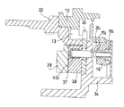
図2および図3には、図1に示した回路を搭載した新撮影レンズ31および新カメラボディ11のマウント部を示している。新撮影レンズ31は、マウントリング32およびバヨネット板33よりも撮影レンズの光軸側に、光軸を中心とした同一円周上に配置された12本のレンズピン35a、35b、35c、35d、35e、35f、35g、35h、35i、35j、35k、35lを備えている。一方、新カメラボディ11は、マウントリング12およびバヨネット板13よりもさらに光軸側に、光軸を中心とした同一円周上にボディピン15a、15b、15c、15d、15e、15f、15g、15h、15i、15j、15k、15lを備えている。レンズピン35a〜35d、35j〜35lの配置は従来の撮影レンズ71のレンズピン75a〜75d、75j〜75lと同一であり、ボディピン15a〜15d、15j〜15lの配置は従来のカメラボディ51のボディピン55a〜55d、55j〜55lと同一である。つまり、5本のボディピン15e、15f、15g、15h、15iおよび5本のレンズピン35e、35f、35g、35h、35iが新たに設けたピンである。
ここで、ボディピン15h、15iがカメラボディ側の所定の第1、第2の接点部材であり、レンズピン35h、35iが撮影レンズ側の第1、第2の接点部材である。
【0017】
新カメラボディ11のボディピン15a〜15lは全て可動ピンであるのに対して、新撮影レンズ31のレンズピン35a〜35lは、可動レンズピン35hを除いて固定ピンである。可動レンズピン35hおよびこれに対応するボディピン15hの構造を、図6を参照して説明する。レンズピン35a〜35lは、絶縁材で形成されたレンズピン保持板38に保持されている。レンズピン保持板38は、導電材で形成されたバヨネット板33に固定されている。可動レンズピン35hは、レンズピン保持板38に形成されたピン穴に出没自在に挿入され、先端部がバヨネット板33および保護環34に形成されたピン穴から突出している。バヨネット板33の外側面(ボディ側面)は、絶縁材で形成された保護環34のフランジ部分で覆われている。
【0018】
レンズピン保持板38の背面には、フレキシブルプリント基板37がプリント基板押え板39によって挟着されて、レンズピン保持板38のピン穴を塞いでいる。フレキシブルプリント基板37の形状を図10に示した。フレキシブルプリント基板37には、レンズピン35a〜35lと接触するコンタクト37a〜37lが形成されていて、各レンズピン35a〜35lは、これらのコンタクト37a〜37lと電気的に導通している。これらのコンタクト37a〜37iは、レンズIC303の入出力端子に接続されている。
ここで、コンタクト37hおよびコンタクト37iは導通している。つまり、可動レンズピン35hとレンズピン35iは導通している。
【0019】
可動レンズピン35hとプリント基板37との間には、導電性部材で形成された圧縮ばね40hが装着されている。この圧縮ばね40hは、プリント基板37のコンタクト37hと可動レンズピン35hに突設されたフランジ36とに接触して可動レンズピン35hを突出方向に付勢するとともに、可動レンズピン35hとコンタクト37hとを導通させている。
この可動レンズピン35hは、新撮影レンズ31が新カメラボディ11に装着されていないときなど、押し込まれていない状態では、圧縮ばね40hの付勢力によって突出し、フランジ36がバヨネット板33に当接させられている(図7参照)。バヨネット板33は接地されているので、この状態では、可動レンズピン35hも接地されている。さらに、可動レンズピン35hはばね40hを介してコンタクト37hと導通しているので、レンズピン35iも同様に接地されている。
【0020】
他のレンズピン35a〜35g、35j〜35lの構造は、図9に示したレンズピン35iと同様である。つまり、レンズピン35iは、レンズピン保持板38に形成されたピン穴に収納され、ばね40iによって、レンズピン35iの後端部がフレキシブルプリント基板37のコンタクト37iに当接するように付勢されている。そしてレンズピン35iは、バヨネット板33および保護環34のフランジ部に形成されたピン穴から突出している。レンズピン35iは、バヨネット板33、その他のコンタクトとは非接触状態を保たれている。
【0021】
新撮影レンズ31が新カメラボディ11に装着されると、可動レンズピン35hは対応するボディピン15hと接触し、ボディピン15hによって、ばね40hの付勢力に抗して押し込まれ、フランジ36がバヨネット板33から離反するので、絶縁される。ボディピン15hは、絶縁材で形成されたボディピン支持板16に形成されたピン穴に挿入され、背面に固定されたプリント基板17との間に装着さればね18によって突出方向に付勢されている。ばね18は、プリント基板17に形成されたコンタクトに接触して、ボディピン18とコンタクトとを導通している。他のボディピン15a〜15g、15j〜15lも同様の構造であり、プリント基板17の対応するコンタクトと導通している。そしてこれらのコンタクトは、プリント基板17を介して新カメラボディ11のDPU103の入出力端子に接続され、CPU101によってDPU103を介して通信制御されている。この実施の形態では、DPU103がインターフェースの機能を有している。
【0022】
この新カメラボディ11および新撮影レンズ31は第2の(新)通信システムに対応している。図4、5に示した第1の(旧)通信対応のカメラボディ51、撮影レンズ71を旧カメラボディ51、旧撮影レンズ71という。
【0023】
本発明の実施の形態は、新撮影レンズ31の可動レンズピン37hおよびレンズピン37iを利用して、新撮影レンズ31と新カメラボディ11の組み合わせであるか、新撮影レンズ31と旧カメラボディ51との組合せであるか、旧撮影レンズ71と新カメラボディ11の組合せであるかを判別可能としたことに特徴を有する。その様子を、図6〜図9と、さらに図11〜図14を参照して説明する。
【0024】
図11〜図14において、新カメラボディ11および旧カメラボディ51のインターフェースの端子に接続されるボディピン15a〜15l、55a〜55lの関係は、下記の通りである。
15a、55a;Fmin2/DATA(判別ピン、データピン)
15b、55b;Fmin1/SCK
15c、55c;Fmax1
15d、55d;Fmax2
15e; − ダミー
15f; − PGND
15g; − VLENS (VBATT)
15h; − LENS N/O
15i; − CONTL/VDD
15j、55j;LS/ACK
15k、55k;Fmin3/RES (リセットピン)
15l、55l;A/M
【0025】
ここで、ボディピン15a〜15d、15j、15k、15lは第1の通信に使用されるピン(第1のボディ接点部材群))であり、ボディピン15a、15b、15h、15i、15kは第2の通信に使用されるピン(第2のボディ接点部材群)である。ボディピン15h、15iは、第1、第2の接点部材として機能し、ボディピン15hは撮影レンズ31の可動レンズピン35hを押圧し、ボディピン15iはカメラボディの電源を撮影レンズに供給するピンである。ボディピン15h、15iは、第2の通信システムの撮影レンズか否かを識別する識別部材としても機能する。
【0026】
新撮影レンズ31においては、これらのボディピン15a〜15lに対応するレンズピン35a〜35lがボディピン同様の機能を有する。つまり、レンズピン35a〜35d、35j、35k、35lは第1の通信に使用されるピン(第1のレンズ接点部材群)であり、レンズピン35a、35b、35h、35i、35kは第2の通信に使用されるピン(第2のレンズ接点部材群)である。可動レンズピン35h、35iは第1、第2の接点部材として機能し、可動レンズピン35hは、新カメラボディ11に装着されたときはボディピン15hに押されてバヨネット板33から離反して絶縁状態となり、レンズピン35iはボディピン15iから所定の電圧、電源の供給を受けるピンとなる。レンズピン35i、可動レンズピン35hは第2の通信システムの撮影レンズであることを識別する識別部材としても機能する。
【0027】
また、新カメラボディ11のマウントリング12およびバヨネットプレート13、新撮影レンズ31のマウントリング32およびバヨネットプレート33は、旧カメラボディと旧撮影レンズの場合と同様に、いずれも金属部材で形成されている。そして、新カメラボディ11に新撮影レンズ31が装着されると、両者のマウントリング12、32、バヨネットプレート13、33が当接し、新カメラボディ11のマウントリング12およびバヨネットプレート13、新撮影レンズ31のマウントリング32およびバヨネットプレート33は、いずれもその電位レベルが接地レベルとなるように形成されている。
すなわち、新または旧カメラボディと、新または旧撮影レンズからなる4通りの装着の組合せがあり、いずれの組合せの場合も、カメラボディ、撮影レンズのマウントリング、バヨネットプレーは同電位、すなわち接地レベルになる。
【0028】
「新レンズ−新ボディ」
新撮影レンズ31が新カメラボディ11に装着された場合、レンズピン35a〜35lはそれぞれ、対応するボディピン15a〜15lに接触する。ここで、可動レンズピン35hは、ボディピン15hによって押し込まれ、バヨネット板33から離反してバヨネット板33とは非導通状態になる(図6および図11(A))。したがって、ボディピン15hおよび15iは、レンズピン35h、35iを介して導通されるので、ボディピン15hおよび15iの一方のレベルは他方のレベルと同一になるから、新カメラボディ11は、このボディピン15iまたは15hのうち、一方のレベルを変化させて他方のレベルをチェックすることで、新撮影レンズ31が装着されたことを判別できる。
【0029】
新カメラボディ11は、新撮影レンズ31が装着されていると判別したときは、ボディピン15iからレンズピン35iを介して電源電圧VDDを新撮影レンズ31に供給し、新撮影レンズ31内のICを起動する。これによって新カメラボディ11は、新撮影レンズ31との間で新通信(第2の通信)の実行が可能になる。
【0030】
「新レンズ−旧ボディ」
新撮影レンズ31が旧カメラボディ51に装着された場合、新撮影レンズ31固有のレンズピン35e〜35iは非接触状態になる(図7、図12(A))。このとき、可動レンズピン35hはバヨネット板33に接地されるので、新撮影レンズ31内のIC回路は、完全にオフする。
しかし、従来配置のレンズピン35a〜35d、35j〜35lは旧カメラボディ51のボディピン55a〜55d、55j〜55lに接触するので、従来配置のピン35a〜35d、35j〜35l、55a〜55d、55j〜55lを利用して従来の通信(第1の通信)処理ができる。
【0031】
「旧レンズ−新ボディ」
旧撮影レンズ71が新カメラボディ11に装着された場合、新カメラボディ11固有のボディピン15e〜15iは非接触(絶縁)状態になる(図8、図13(A))。このとき、ボディピン15hおよび15iはお互いに全く独立の非導通状態のままであるから、新カメラボディ11は、このボディピン15hまたは15iの一方のレベルを変化させて他方のレベルをチェックすること、つまり一方のレベルを変化させても他方のレベルが変化しない、または一方のレベルと他方のレベルとが相違することを検知することで、旧撮影レンズ71が装着されたことを判別できる。
そして、従来配置のボディピン15a〜15d、15j〜15lは旧撮影レンズ71のレンズピン75a〜75d、75j〜75lに接触するので、従来配置のピン15a〜15d、15j〜15l、75a〜75d、75j〜75lを利用して従来の通信(第1の通信)処理ができる。つまり、
【0032】
「旧レンズ−旧ボディ」
旧撮影レンズ71が旧カメラボディ51に装着された場合は、旧撮影レンズ71のレンズピン75a〜75d、75j〜75lと旧カメラボディ51のボディピン55a〜55d、55j〜55lとが接触することは、従来通りであり、従来の通信(第1の通信)処理ができる。
【0033】
図15は、新撮影レンズ31の入出力回路をブロックで示している。この実施例は、ROM303aを備えたレンズIC303、およびCPUを備えた電子回路に適用できる。レンズIC303は、4個の入出力端子( リセット端子RES 、シリアルクロック端子 ̄SCK  ̄、シリアルデータ入出力端子SIO 、電力端子VCC)を介してカメラボディと通信を行い、電力供給を受け、3個の入力端子DIS1〜DIS3から距離コードを入力し、4個の入力端子ZOOM1 〜ZOOM4 からズームコードを入力する。
【0034】
カメラ通信用のリセット端子RES はレンズピン35k(Fmin3/RES )に接続され、端子 ̄SCK  ̄はレンズピン35b(Fmin1/SCK )に接続され、シリアルデータ入出力端子SIO はレンズピン35a(Fmin2/DATA)に接続され、電力端子VCCはレンズピン35i(CONTL/VDD)に接続されている。
なお、アクノレッジ端子ACK は、レンズIC303に替えて、CPUが搭載された場合に使用されるものであり、レンズIC303が搭載されている場合は使用されない。レンズCPUは、パワーオンした後、発振子により発振を開始し、発振が安定してから初期化プログラム時に端子ACK を立ち下げ、初期化が終了したら端子ACK を立ち上げて待機状態をカメラボディに伝える。新カメラボディ11は、これによってCPUを備えた撮影レンズであることを判別し、その後新撮影レンズとの間で、オペレーションコード通信、データ通信などを行う。
【0035】
レンズピン35k(Fmin3/RES )、レンズピン35b(Fmin1/SCK )およびレンズピン35a(Fmin2/DATA)は、その撮影レンズの開放絞りFナンバーに対応するコードに応じてショットキーバリアダイオードを介してレンズピン35i(CONTL/VDD)と接続されている。つまり、旧カメラボディ51に装着されたときは可動レンズピン35hが接地するのでレンズピン35i(CONTL/VDD)も接地し、レンズピン35i(CONTL/VDD)にショットキーバリアダイオードを介して接続されたレンズピン35k(Fmin3/RES )、レンズピン35b(Fmin1/SCK )およびレンズピン35a(Fmin2/DATA)はショットキーバリアダイオードによる順方向電圧降下分VF レベルのためローレベルとなり、ショットキーバリアダイオード未接続の端子はハイレベルになるので、開放絞りFナンバーを旧カメラボディ51に送ることができる。
【0036】
そして、新カメラボディ11に装着されると、可動レンズピン35hはバヨネット板33から離反し、レンズピン35iと同電位になる。レンズピン35iには新カメラボディ11から電源電圧VDDが供給されるため、レンズピン35k(Fmin3/RES )、レンズピン35b(Fmin1/SCK )およびレンズピン35a(Fmin2/DATA)のショットキーバリアダイオードは絶縁状態になり、これらのピンを使ってシリアル通信による情報の授受ができる。なお、ダイオードにショットキーバリアダイオードを使っているのは、順方向電圧降下分VF による影響を小さくするためであり、カメラボディ側の回路がローレベルと判断できる辯値が十分高ければ、通常のダイオードを使用できる。
【0037】
また、最小絞りのFナンバーを旧カメラボディ51に送るために、レンズピン35c、35d(Fmax1 、Fmax2 )は最小絞りFナンバーに応じて接地され、絞りオートかマニュアルかを識別するレンズピン35l(A/M )が絞りリングの状態により接地またはフローティングされている。
【0038】
レンズICを搭載した新レンズには、レンズ側で独自に演算制御が可能なレンズCPU搭載レンズと、レンズCPUは有さないレンズ(以下「LROMレンズ」という)の2種類を有する。したがって、カメラボディにレンズが装着された際に、カメラボディは第2の通信が可能か否かの判別を行った後、第2の通信方式による通信動作内において、改めて装着されている撮影レンズがレンズCPUを搭載したレンズか否かの判別を行う必要がある。
【0039】
図16には、レンズCPUを有さない、新撮影レンズ31におけるレンズIC303の入出力回路の要部を示し、図17には、データ通信時のタイミングチャートを示している。ROM303aが搭載されている新撮影レンズ31の場合は、図16に示すように、リセット端子RES に入力される信号がハイレベル(リセット信号)からローレベル(リセット解除信号)に切り換わったときにシリアルデータ入出力端子SIO の出力レベルをローにするための応答手段として応答回路303Rが設けられている。この応答回路303Rは、DフリップフロップF1、インバータG3、G5、ANDゲートG1、G4、ノアゲートG2、トランジスタ(nチャネルFET)T1、T2から構成されている。なお、レンズICがレンズCPUである場合は、図示しないが、このような応答回路はなく、各端子Fmin3/RES 、Fmin1/sck、Fmin2/DATA、CONTL/VDDは、レンズCPUの対応するポートに直接接続された構成となる。ここで、トランジスタT1が第1のスイッチ手段として機能し、トランジスタT2が第2のスイッチ手段として機能する。
【0040】
電源電圧VDDが供給され、リセット端子RES がハイレベルのときは、インバータG3の入力はハイレベル、出力はローレベル、ノアゲートG2の一方の入力がハイレベルなので出力はローレベル、AND ゲートG1は一方の入力がローレベルなので出力はローレベル、したがってトランジスタ(nチャネルFET)T1、T2は共にローでオフ状態なので、シリアルデータ入出力端子SIO はハイインピーダンス状態にある。ここで、リセット端子RES がローレベルに立ち下がると、AND ゲートG4の入力はローレベルなので出力はローレベル、ノアゲートG2の入力は共にローレベルなので出力はハイレベル、したがってトランジスタT2がオンするので、シリアルデータ入出力端子SIO はローレベルに立ち下がる。
リセット端子RES がローレベルの状態でクロック端子SCK にクロックが入ると、DフリップフロップF1のQ出力は、シリアル端子クロックの一番最初の立ち下がりに同期してローからハイの信号が出力される。クロックはカウンタ3031にも入力され、デコーダ3032、パラ−シリ変換器3033を介して、ROM303aから読み出された1バイトデータがシリアル変換されてAND ゲートG4の一方に入力される。AND ゲートG4の他方の入力にはDフリップフロップF1のQ出力が入力されているので、シリアルクロックの一番最初の立ち下がり後に、パラ−シリ変換器3033の出力がAND ゲートG4から出力される。
【0041】
AND ゲートG4の出力がハイレベルのときは、AND ゲートG1の一方の入力はハイ、他方の入力は、リセット端子RES のローレベルがインバータG3によって変換されたハイレベルなのでAND ゲートG1の出力はハイレベルになってトランジスタT2がオフし、トランジスタT1がオンして、シリアルデータ入出力端子SIO からハイレベルデータが出力される。AND ゲートG4の出力がローレベルのときは、ノアゲートG2の出力がハイになってトランジスタT2がオンし、一方ANDゲートG1の出力はローレベルになってトランジスタT1がオフするので、シリアルデータ入出力端子SIO からローレベル信号が出力される。
【0042】
以上のように、リセット端子RES がハイレベルのときにはシリアルデータ入出力端子SIO はハイインピーダンス状態で、カメラボディ側のプルアップ抵抗によりハイレベルになり、その後リセット端子がローレベルに落ちると、シリアルデータ入出力端子SIO はローレベルに落ち、その後シリアルクロックがシリアルクロック端子SCK に入力されると、シリアルデータ入出力端子SIO からデータが逐次出力される(図17参照)。
なお、ROM303aからデータを読み出すときは、アドレスとして、ズームコード板306から入力されるコード信号をアドレス入力回路3034でラッチして取り込んでいる。
【0043】
通常、CPUに比してレンズIC(ROM IC)は起動時間がかからない。例えば、CPUは、電源投入後、発振安定待ち時間後に内部RAM、端子などをイニシャライズしてからコマンドの受け付けを開始する。そのため、ROM ICを搭載しているのかCPUを搭載しているのかを判別するためには、CPUが正常に応答して動作に入る時間待たなければ判別できなかった。
本発明の実施の形態のように、レンズCPUが搭載されていない撮影レンズ、すなわち、ROM ICは搭載されている撮影レンズにおいては応答回路303Rを設けて、カメラボディ側のCPUからの制御信号(端子RESのハイまたはロー)に対応する応答信号の応答出力速度を意図的に速めるように構成している。一方、カメラボディ側のCPUにおいては、この応答速度の違いにより装着されている撮影レンズがCPUを搭載しているのか否かを判断するようにしているので、カメラボディ側CPUの起動時間を考慮せずに短時間で判別ができる。
【0044】
本発明の実施の形態は、ROM ICを搭載した新レンズの判別を短時間で終了できるカメラシステムを提供する。このカメラシステムの動作について、図18から図26に示したフローチャートを参照して説明する。
図18は、このカメラボディのメイン処理の概要を示すフローチャートである。このメイン処理には、メインスイッチがオンされたときに入るものとする。
メイン処理をスタートすると、まず、CPU101、DPU103の端子をイニシャライズし、RAM もイニシャライズする(S101、S103)。
次に、本発明の実施例の特徴であるレンズチェック処理を実行する(S105)。このレンズチェック処理で、第1の通信レンズであるか、第2の通信レンズであるか、さらにその詳細を判別する。
【0045】
レンズの判別が終了したら、測光スイッチがオンしているかどうかをチェックし、オンしていなければレンズ判別処理に戻り(S107;N、S105)。オンしていれば、AF処理およびAE演算処理を実行する(S107;Y、S109、S111)。そして、レリーズスイッチがオンしていなければそのままS105に戻り(S113;N、S105)、レリーズスイッチがオンしていればレリーズ処理を実行してS105に戻る(S113;Y、S115、S105)。
【0046】
図19、20は、装着されたレンズの種別を判別するフローチャートである。レンズ判別処理に入ると、まず、レンズCPUを備えたレンズかどうかをチェックする(S201)。一番最初の状態ではレンズの種類が不明なので、S223に進む(S201;N、S223)。CPUを備えたレンズであれば、LENSNGフラグが0かどうかをチェックし、0であればS205に進む(S201;Y、S203、S205)。CPUを備えていないレンズか、備えていてもLENSNGフラグに“0”がセットされていたらS223に進む(S201;N、S223、またはS201;Y、S203;N、S223)。
【0047】
S205では、マウントピンチェック処理(check_mount_pin )を実行する。マウントピンチェック処理は、図22にそのフローチャートを示したように、端子Fmax1、Fmax2、A/M、LSレベルを入力し(S501)、端子Fmax1、FMmax2のレベル変化があったかどうかをチェックして、変化があればマウント変化フラグに“1”をセットし(S503;Y、S505)、変化がなければマウント変化フラグを“0”にする処理である(S503;N、S507)。
この処理において、マウントレベルが変化したと判断した場合にはLENS0処理に進む(S207;Y)。マウントレベルが変化していないと判断したときには、LENSNGフラグをクリアして、レンズCPUによるレンズROM通信を実行して通信ができたかどうかをチェックする(S211、S213)。通信OKでなければ通信不可である旨を識別するLCPU NG フラグに“1”をセットしてリターンし(S211、S213;N、S215)、通信OKであればS215をスキップしてリターンする(S213;Y)。
【0048】
S201、S203のチェック処理からS223に来ると、LENS NG フラグが“0”かどうかをチェックし、LENS NG フラグに“0”がセットされていなければLENS0処理に進む(S223;N)。次に、レンズ種別が0かどうかをチェックし、0であればLENS0処理に進む(S223;Y、S225;Y)。レンズ種別が0でないときは、レンズ種別がKレンズかAレンズかをチェックし、いずれかであればLENS0処理に進み(S225;N、S227;Y)、いずれでもなければ、マウントピンチェック処理(check_mount_pin)を実行する(S225;N、S227;N、S229)。そして、マウント変化フラグに“1”がセットされているかどうかをチェックし、セットされていればLENS0処理を実行する(S229、S231;Y)。マウント変化フラグに“1”がセットされていなければ、リターンする。
【0049】
LENS0処理について、図20を参照して説明する。LENS0処理は、新旧レンズ判別およびレンズIC/レンズCPUチェック処理である。
LENS0処理に入ると、まず、LENS_kindデータおよびLENSNGフラグに“0”をセットしてマウントピン入力処理(in_mount_pin)を実行する(S301、S303)。マウントピン入力処理は、図23にそのフローチャートを示したように、端子Fmax1〜2、Fmin1〜3 、A/M 、LSレベルを入力し(S551)、端子Fmax1 、Fmax2 のレベル変化があったかどうかをチェックして、変化があればマウント変化フラグに“1”をセットし(S553;Y、S555)、変化がなければマウント変化フラグに“0”をセットする処理である(S553;N、S557)。
【0050】
次に、端子CONTL のレベルをローレベル(グランド)に落とし、端子LENSN/Oがハイレベルになったかどうかをチェックする(S305、S307)。ハイレベルであれば、図13(A)に示した旧レンズであることが分かるので、S309の旧レンズチェック処理(ka_lens_shori )を実行してリターンする(S307;Y、S309)。
【0051】
旧レンズチェック処理は、レンズが装着されていないか、開放、最小絞り情報の無いレンズ(Kレンズ)が装着されているか、開放、最小絞り情報を有するレンズ(Aレンズ)が装着されているかどうかをチェックする処理である。
図24に示した旧レンズチェック処理に入ると、すべてのボディピン(マウント入力端子)のレベルがハイレベルかどうかをチェックし、すべてがハイレベルであればボディピン15a〜15lがレンズピンに接触していないので、フラグNO LENS に1をセットしてリターンする(S601;Y、S603)。いずれかのボディピンのレベルがハイレベルでなければ、全てのボディピンのレベルがローレベルかどうかをチェックし、全てローレベルであればフラグK LENSに1をセットし(S601;N、S605;Y、S607)、すべてがローレベルでなければフラグA LENSに1をセットしてリターンする(S601;N、S605;N、S609)。
【0052】
S307のチェックにおいて、端子LENS N/Oがハイレベルではなかったら、リセット端子RES および端子CONTL/VDDをハイレベルに立ち上げて端子LENS N/Oがハイレベルに変わったかどうかをチェックする(S307;N、S311、S313、S315)。図11(A)に示した新レンズが装着されていれば端子LENSN/Oは端子CONTL/VDD と同一のレベルになるので、端子LENS N/Oがハイレベルであれば新レンズと判断してS317に進み(S315;Y、S317)、端子LENSN/Oがハイレベルでなければ新レンズではないか異状なのでS309に進む(S315;N、S309)。
【0053】
S317ではリセット端子RES をローレベルに落とし、S319で端子Fmin2/DATA(SIO )がローレベルかどうかをチェックする。端子Fmin2/DATAがローレベルに落ちていれば、図16で示したようにROM ICを搭載した新レンズなので、図27に示したようにLROM通信を実行してリターンする(S319;Y、S321)。
【0054】
端子Fmin2/DATAがローレベルに落ちていなければ、レンズCPUを搭載した新レンズと判別し、レンズCPU搭載撮影レンズであることを識別するフラグLCPULENS に1をセットしてリセット端子RES をハイレベルに立ち上げる(S319;N、S323、S325)。次に、端子LS/ACKのレベルが立ち下がり、そして立ち上がるのをタイマーループ処理によって待つ(S327、S329)。
所定時間内に端子LS/ACKのレベルが落ちて立ち上がらなかったら、異常であることを識別するLCPU NG フラグに“1”をセットしてリターンする(S327;N、S337またはS327;Y、S329;N、S337)。
所定時間内に端子LS/ACKのレベルが落ちて立ち上がったらレンズCPUは正常動作をしているので、S331に進んでLROM_CPU通信を実行する(S327;Y、S329;Y、S331)。そして、正常な通信ができればLENS1処理に進み(S333;Y)、正常な通信ができなかったらレンズCPUが異常である旨を識別するLCPU NG フラグに“1”をセットしてLENS1処理に進む(S333;N、S335)。
【0055】
以上の通り、レンズCPUを持たない撮影レンズの場合は、応答回路303Rが設けられているので、S317のステップの動作に対して、応答回路303Rにより直ちに端子Fmin2/DATAにローレベル信号が現れて、装着レンズがレンズCPUを持たない撮影レンズであることを判別できる。別言すると、装着レンズが旧レンズが新レンズかの判別をするために、リセット端子RESをローレベルからハイレベルに変化させたものを、元のローレベルに戻した段階で、直ちに、装着レンズがレンズCPUを持たない装着レンズか否かを判別できる。
【0056】
次に、LENS1処理について、図21を参照して説明する。
ここでは、新撮影レンズ31から入力した通信データによりLROM通信コードがOKかどうかをチェックし、OKでなければ、LCODENG フラグに“1”をセットしてS405に進み(S401;N、S403、S405)、OKであればこのセット処理をスキップしてS405に進む(S401;Y、S405)。S405では、レンズCPUを備えたレンズかどうかをチェックし、レンズCPU搭載レンズでなければフラグLROM lens に1をセットしてリターンし(S405;N、S407)、レンズCPU搭載レンズであればそのままリターンする(S405;Y)。
【0057】
以上の通り本実施の形態によれば、ROM ICを搭載した新撮影レンズ31の場合、リセット端子RES のレベルがハイからローに変わるとほぼ同時に端子Fmin2/DATA(SIO )のレベルもハイからローに変わるが、レンズCPUを搭載した撮影レンズの場合は、リセット端子RES でリセットを解除してもCPUのパワーオンリセット処理に時間を要し、端子Fmin2/DATA(SIO )は反応しないので、リセット端子RES をローレベルに落として端子Fmin2/DATA(SIO )のレベルがローかハイかをチェックすればROM ICを搭載した新撮影レンズであるか、レンズCPUを搭載した新撮影レンズであるかが直ちに判断できるので、以後の処理時間を短縮できる。
【0058】
S321で実行されるLROM通信処理を、図25に示したフローチャートおよび図27のタイミングチャートを参照して説明する。LROM通信処理に入ると、受信データ数(バイト数)をカウントするカウンタnに0をセットする(S651)。そして、受信データアドレスLC(n)のRAMに受信したデータを格納する(S653)。その後、シリアル通信を実行し、カウンタnを1インクリメントして、16になったかどうかをチェックし、16になるまで上記処理を繰り返して待つ(S655、S657;N、S653)。
カウンタnが16になったら、リターンする(S657;Y)。つまり、本実施例では、撮影レンズのROMから16バイト分のデータを受信する。
【0059】
S211他で実行されるLROM_CPU通信処理について、図26に示したフローチャートおよび、図28のタイミングチャートを参照して説明する。LROM_CPU通信処理は、制御手段(CPU)を搭載した撮影レンズであると判別したときに入る処理である。LROM_CPU通信処理に入ると、まず、端子LS/ACKがローレベルかどうかをチェックする(S701)。端子LS/ACKがローレベルに落ちていたら、リセット端子RES をハイレベルに立ち上げてリセットをかけ、通信エラーフラグに“1”をセットしてリターンする(S701;Y、S731、S733)。
【0060】
端子LS/ACKがローレベルでなければ、リセット端子RES のレベルをローレベルに落としてタイマーにより端子LS/ACKのレベルがローレベルに落ちたかどうかをチェックし(S701;N、S703、S705)、タイマー時間内にローレベルに落ちなかったらリセット端子RES をハイレベルに立ち上げてリセットをかけ、通信エラーフラグに“1”をセットしてリターンする(S705;N、S731、S733)。
端子LS/ACKがローレベルに落ちたらオペレーションコードを出力し、カウンタnに0をセットして端子LS/ACKが立ち上がるかどうかをチェックする(S705;Y、S707、S709、S711)。オペレーションコード出力に応答して端子LS/ACKがハイレベルに立ち上がらなかったらリセット端子RES をハイレベルに立ち上げ、通信エラーフラグに“1”をセットしてリターンする(S711;N、S731、S733)。
【0061】
オペレーションコード出力に応答して端子LS/ACKがハイレベルに立ち上がったらリセット端子RES をハイレベルに立ち上げて、端子LS/ACKがローレベルに落ちるかどうかをチェックし、落ちなかったらリセット端子RES をハイレベルに立ち上げ、通信エラーフラグ1をセットしてリターンする(S711;Y、S713、S715;N、S731、S733)。端子LS/ACKがローレベルに落ちたら、リセット端子RES をローレベルに落として、レンズCPUからデータを受信し、受信したデータをRAMの受信データアドレスLC(n)に逐次格納する(S715;Y、S717、719)。そして、カウンタnを1インクリメントして、カウンタが16になったかどうかをチェックし、16になるまで上記処理を繰り返す(S721、S723;N、S711)。
【0062】
カウンタが16になったら、端子LS/ACKがハイレベルに立ち上がるかどうかをチェックし、立ち上がったらリセット端子RES をハイレベルに立ち上げてリターンする(S723;Y、S725;Y、S729)。端子LS/ACKがハイレベルに立ち上がらなかったら通信エラーフラグに“1”をセットし、リセット端子RESをハイレベルに立ち上げてリターンする(S725;N、S727、S729)。
【0063】
撮影レンズにCPUを搭載するのは、例えばAFモータを搭載して、AFモータの駆動制御をレンズCPUに実行させる場合、またはレンズシャッタを搭載して、レンズシャッタの駆動制御を撮影レンズに搭載したシャッタモータの駆動制御によりレンズCPUに行わせる場合などである。そのためには、ボディCPUとレンズCPUとの間で、必要なコマンド、データなどをさらに所定のプロトコルで通信する。そしてレンズCPUは、通信によって授受した情報に基づいて動作する。
【0064】
【発明の効果】
以上の説明から明らかな通り本発明は、制御手段を有さない記憶手段を搭載した撮影レンズには、カメラボディ側からリセットピンにリセット解除信号を受けると判別ピンのレベルが変わる応答手段を備えたので、カメラボディは、リセットピンにリセット解除信号を出力して判別ピンのレベル変化を検知することで記憶手段を搭載した撮影レンズかどうかを判別することが可能になり、その後の処理を迅速に実行できる。
【図面の簡単な説明】
【図1】本発明を適用した一眼レフカメラの一実施の形態の主要回路構成をブロックで示す図である。
【図2】同一眼レフカメラの新撮影レンズのマウント部を示す図である。
【図3】同一眼レフカメラの新カメラボディのマウント部を示す図である。
【図4】従来の一眼レフカメラの旧撮影レンズのマウント部を示す図である。
【図5】従来の一眼レフカメラの旧カメラボディのマウント部を示す図である。
【図6】新撮影レンズを新カメラボディに装着したときの、可動レンズピンの構造を示す要部の断面図である。
【図7】新撮影レンズを旧カメラボディに装着したときの、可動レンズピンの様子を示す要部の断面図である。
【図8】旧撮影レンズを新カメラボディに装着したときの、可動レンズピンと接触し得るボディピンの様子を示す要部の断面図である。
【図9】新撮影レンズを新カメラボディに装着したときの、新レンズピンの様子を示す要部の断面図である。
【図10】新撮影レンズのレンズピンと導通するプリント基板の形状を示す図である。
【図11】新撮影レンズを新カメラボディに装着したときの新レンズピン、新ボディピンの状態を説明する図である。
【図12】新撮影レンズを旧カメラボディに装着したときの新レンズピンの状態を説明する図である。
【図13】旧撮影レンズを新カメラボディに装着したときの新ボディピンの状態を説明する図である。
【図14】旧撮影レンズを旧カメラボディに装着したときのレンズピンおよびボディピンの状態を説明する図である。
【図15】新撮影レンズの入出力端子とレンズピンとの関係を説明する図である。
【図16】新撮影レンズの入出力回路の要部を示す回路図である。
【図17】同入出力回路の入出力のタイミングチャートを示す図である。
【図18】新カメラボディのメイン処理に関するフローチャートを示す図である。
【図19】新カメラボディのレンズチェック処理に関するフローチャートを示す図である。
【図20】同新カメラボディのレンズチェック処理0に関するフローチャートを示す図である。
【図21】同新カメラボディのレンズチェック処理1に関するフローチャートを示す図である。
【図22】同新カメラボディのマウントチェック処理に関するフローチャートを示す図である。
【図23】同新カメラボディの別のマウントチェック処理に関するフローチャートを示す図である。
【図24】同新カメラボディのKaレンズ処理に関するフローチャートを示す図である。
【図25】同新カメラボディのレンズROM通信処理に関するフローチャートを示す図である。
【図26】同新カメラボディのレンズROM_CPU通信処理に関するフローチャートを示す図である。
【図27】同新カメラボディとROMを搭載している新撮影レンズの通信タイミングチャートを示す図である。
【図28】同新カメラボディとCPUを搭載している新撮影レンズの通信タイミングチャートを示す図である。
【符号の説明】
11 新カメラボディ
15a 15b 15c 15d 15j 15k 15l 旧ボディピン
15e 15f 15g 新ボディピン
15h 新ボディピン
15i 新ボディピン
31 新撮影レンズ
35a 35b 35c 35d 35j 35k 35l 旧レンズピン
35e 35f 35g 新レンズピン
35h 可動レンズピン
35i 新レンズピン
51 旧カメラボディ
55a 55b 55c 55d 55j 55k 55l ボディピン
71 旧撮影レンズ
75a 75b 75c 75d 75j 75k 75l レンズピン
101 CPU
103 DPU
303 レンズIC
303a レンズROM
T1 トランジスタ(第1のスイッチ手段)
T2 トランジスタ(第2のスイッチ手段)[0001]
TECHNICAL FIELD OF THE INVENTION
The present invention relates to a single-lens reflex camera provided with an information transmitting pin (contact member) at a place other than the mounting surface, and particularly to a photographic lens, a camera body, and a camera system of a so-called medium-format single-lens reflex camera.
[0002]
[Prior art and its problems]
Some conventional single-lens reflex cameras include a pin group for transmitting information as a plurality of contact pins for identifying open aperture data and minimum aperture data at a location other than the mounting surface of the photographing lens, for example, inside the mounting surface. A lens pin group) is provided, and an information transmission pin group (body pin group) as a plurality of contact pins in contact with the information transmission pin group is provided around the mount of the camera body. In some cameras, the potential (level) is checked and opened, and the minimum aperture data is input to the camera body.
[0003]
2. Description of the Related Art In recent years, there has been a demand for functions not available in conventional photographing lenses and camera bodies. A problem that arises when a new function is provided in a photographing lens and a camera body is compatibility between a new and old photographing lens and a camera, particularly, compatibility regarding a lens, a contact member for transmitting and receiving body information, and a communication method.
[0004]
FIGS. 4 and 5 show a conventional photographing lens and a mounting portion of a camera body. The group of aperture information setting pins (contact members) is a
[0005]
The
[0006]
By the way, in order to provide such a photographing lens with a new function, for example, mounting a ROM, further mounting an AF motor and its control means, and mounting a lens shutter and its control means require conventional methods. The
[0007]
[Object of the invention]
The present invention has been made in view of the problems of conventional lenses, camera bodies, and camera systems, and has been developed to provide a new function of a shooting lens, camera body, and camera system that is compatible with existing shooting lenses and camera bodies. The purpose is to provide.
[0008]
Summary of the Invention
2. A camera body according to
The photographic lens of the present invention is a photographic lens that includes a plurality of contact pins including a reset pin and a determination pin, and performs information transmission through contact of these contact pins when the camera body is mounted. The photographing lens has storage means without control means, and the level of the determination pin when a reset release signal is received from the camera body to the reset pin. And a response unit that, when a reset release signal is given to the reset pin, synchronizes with the clock input from the camera body via another contact pin, and stores the response signal in the storage unit. Output the written data from the determination pin It is characterized by:
In the camera system of the present invention, each of the photographing lens and the camera body includes a plurality of contact pins including a reset pin and a determination pin. When the photographing lens is mounted on the camera body, contact of these contact pins is performed. Camera system that transmits information via a memory, equipped with storage means without control means The shooting lens When the reset pin receives a reset release signal from the camera body, Change level A response unit, wherein the camera body outputs a reset release signal to a reset pin, detects a level change of a determination pin, and includes a determination unit for determining whether or not the imaging lens has the storage unit. The determining means of the camera body outputs a clock to the photographic lens via another contact pin when it is determined from the level change of the determining pin that the photographic lens is provided with the storage means, and The lens determination means inputs a clock output from the camera body from another contact pin, and outputs data read from the storage means by the clock to the camera body from the determination pin. It is characterized by:
[0009]
BEST MODE FOR CARRYING OUT THE INVENTION
The present invention will be described below with reference to the drawings. FIG. 1 is a block diagram showing a main circuit of a single-lens reflex camera according to an embodiment of the present invention. The optical system and mechanical configuration of this single-lens reflex camera are not shown because they are known. Hereinafter, the camera body of the single-lens reflex camera is referred to as a
[0010]
The input terminals of the
[0011]
When the photometric switch SWS is turned on, a subject luminance signal is input from the
[0012]
When the release switch SWR is turned on, the
[0013]
The new photographing
[0014]
Next, an embodiment relating to a pin structure as a contact member of the taking lens and the camera body of the present invention will be described.
Lens pins and body pins as contact members for reading data between the photographic lens and the camera body are compatible with photographic lenses and photographic cameras that are mounted inside the mount and mounting surface. However, in order to add a new function, a lens pin group and a body pin group are newly provided as first and second contact members in addition to the conventional lens pin group and the body pin group. One of the lens pins (the first contact member) in the new lens pin group is made movable, and the other lens pin (the second contact member) is brought into conduction, and the movable lens pin protrudes. In this state, it was formed to be electrically connected to the lens-side mount as a ground member, and to be insulated from the lens-side mount when pushed in.
[0015]
When the new shooting lens is attached to the new camera body, the movable lens pin is pushed by the corresponding new body pin on the new camera body, and becomes insulated from the lens side mount, and is attached to the old camera body. Sometimes, a new lens pin group of the new photographic lens is in a non-contact state with the body pin group of the old camera body, and the movable lens pin and the other lens pins are both grounded to the lens-side mount.
[0016]
FIG. 2 and FIG. 3 show a mounting portion of the new photographing
Here, the body pins 15h and 15i are predetermined first and second contact members on the camera body side, and the lens pins 35h and 35i are first and second contact members on the photographing lens side.
[0017]
While the body pins 15a to 15l of the
[0018]
On the rear surface of the lens
Here, the
[0019]
A
When the
[0020]
The structure of the
[0021]
When the new photographing
[0022]
The
[0023]
The embodiment of the present invention uses the
[0024]
11 to 14, the relationship between the body pins 15a to 15l and 55a to 55l connected to the interface terminals of the
15a, 55a; Fmin2 / DATA (discrimination pin, data pin)
15b, 55b; Fmin1 / SCK
15c, 55c; Fmax1
15d, 55d; Fmax2
15e;-dummy
15f;-PGND
15 g;-VLENS (VBATT)
15h;-LENS N / O
15i;-CONTL / VDD
15j, 55j; LS / ACK
15k, 55k; Fmin3 / RES (reset pin)
15 l, 55 l; A / M
[0025]
Here, the body pins 15a to 15d, 15j, 15k, and 15l are pins (first body contact member group) used for the first communication, and the body pins 15a, 15b, 15h, 15i, and 15k are 2 is a pin (second body contact member group) used for communication No. 2. The body pins 15h and 15i function as first and second contact members, the
[0026]
In the new photographing
[0027]
The
That is, there are four types of mounting combinations including a new or old camera body and a new or old photographing lens, and in any case, the camera body, the mount ring of the photographing lens, and the bayonet play have the same potential, that is, the ground level. become.
[0028]
"New lens-new body"
When the new photographing
[0029]
When the
[0030]
"New lens-old body"
When the new photographing
However, since the conventionally arranged
[0031]
"Old lens-new body"
When the old photographing
Since the conventionally arranged body pins 15a to 15d and 15j to 15l contact the lens pins 75a to 75d and 75j to 75l of the old photographing
[0032]
"Old lens-old body"
When the old photographing
[0033]
FIG. 15 shows an input / output circuit of the new photographing
[0034]
The camera communication reset terminal RES is connected to the
The acknowledgment terminal ACK is used when a CPU is mounted instead of the
[0035]
The
[0036]
Then, when the
[0037]
In order to send the minimum aperture F number to the
[0038]
New lenses equipped with a lens IC include two types of lenses: a lens with a lens CPU that can be independently operated and controlled on the lens side, and a lens without a lens CPU (hereinafter referred to as an “LROM lens”). Therefore, when the lens is mounted on the camera body, the camera body determines whether or not the second communication is possible, and then performs the newly mounted shooting lens in the communication operation using the second communication method. It is necessary to determine whether is a lens equipped with a lens CPU.
[0039]
FIG. 16 shows a main part of an input / output circuit of the
[0040]
When the power supply voltage VDD is supplied and the reset terminal RES is at a high level, the input of the inverter G3 is at a high level, the output is at a low level, and one of the inputs of the NOR gate G2 is at a high level, the output is at a low level, and the AND gate G1 is at one. Is low, the output is low, and therefore, the transistors (n-channel FETs) T1 and T2 are both low and off, so that the serial data input / output terminal SIO is in a high impedance state. Here, when the reset terminal RES falls to a low level, the output of the AND gate G4 is at a low level because the input of the AND gate G4 is at a low level, and the output of the NOR gate G2 is at a high level because both inputs of the NOR gate G2 are at a low level. The serial data input / output terminal SIO falls to a low level.
When a clock is input to the clock terminal SCK while the reset terminal RES is at the low level, the Q output of the D flip-flop F1 outputs a low-to-high signal in synchronization with the first falling of the serial terminal clock. . The clock is also input to the
[0041]
When the output of the AND gate G4 is high, one input of the AND gate G1 is high, and the other input is high because the low level of the reset terminal RES is converted to the high level by the inverter G3. At this level, the transistor T2 is turned off, the transistor T1 is turned on, and high-level data is output from the serial data input / output terminal SIO. When the output of the AND gate G4 is at a low level, the output of the NOR gate G2 becomes high and the transistor T2 is turned on, while the output of the AND gate G1 is at a low level and the transistor T1 is turned off. A low level signal is output from the terminal SIO.
[0042]
As described above, when the reset terminal RES is at a high level, the serial data input / output terminal SIO is in a high impedance state. The serial data input / output terminal SIO goes to a high level by a pull-up resistor on the camera body side. When the input / output terminal SIO falls to a low level and a serial clock is thereafter input to the serial clock terminal SCK, data is sequentially output from the serial data input / output terminal SIO (see FIG. 17).
When data is read from the
[0043]
Normally, a lens IC (ROM IC) requires less startup time than a CPU. For example, after turning on the power, the CPU initializes the internal RAM, terminals, and the like after an oscillation stabilization wait time, and then starts accepting a command. Therefore, in order to determine whether a ROM IC is mounted or whether a CPU is mounted, it is not possible to determine whether the CPU has to respond normally and wait for the operation to start.
As in the embodiment of the present invention, a
[0044]
Embodiments of the present invention provide a camera system that can end determination of a new lens equipped with a ROM IC in a short time. The operation of the camera system will be described with reference to the flowcharts shown in FIGS.
FIG. 18 is a flowchart showing an outline of the main processing of the camera body. This main process is started when the main switch is turned on.
When the main processing is started, first, the terminals of the
Next, a lens check process which is a feature of the embodiment of the present invention is executed (S105). In this lens check process, it is further determined whether the lens is the first communication lens or the second communication lens.
[0045]
When the lens determination is completed, it is checked whether or not the photometry switch is on. If not, the process returns to the lens determination process (S107; N, S105). If it is on, the AF process and the AE calculation process are executed (S107; Y, S109, S111). If the release switch is not on, the process returns to S105 (S113; N, S105). If the release switch is on, the release process is executed and the process returns to S105 (S113; Y, S115, S105).
[0046]
19 and 20 are flowcharts for determining the type of the attached lens. In the lens determination process, first, it is checked whether the lens has a lens CPU (S201). Since the type of the lens is unknown in the first state, the process proceeds to S223 (S201; N, S223). If the lens has a CPU, it is checked whether the LENSNG flag is 0, and if it is 0, the process proceeds to S205 (S201; Y, S203, S205). If the lens does not have a CPU, or if the lens does have a LENSNG flag set to "0", the process proceeds to S223 (S201; N, S223, or S201; Y, S203; N, S223).
[0047]
In S205, a mount pin check process (check_mount_pin) is executed. In the mount pin check process, as shown in the flowchart of FIG. 22, the terminals Fmax1, Fmax2, A / M, and LS level are input (S501), and it is checked whether or not the levels of the terminals Fmax1, FMmax2 have changed. If there is a change, the mount change flag is set to "1"(S503; Y, S505). If there is no change, the mount change flag is set to "0"(S503; N, S507).
In this process, if it is determined that the mount level has changed, the process proceeds to the LENS0 process (S207; Y). If it is determined that the mount level has not changed, the LENSNG flag is cleared, and lens ROM communication by the lens CPU is executed to check whether communication has been completed (S211 and S213). If the communication is not OK, "1" is set to the LCPU NG flag for identifying that communication is impossible, and the process returns (S211, S213; N, S215). If the communication is OK, the process skips S215 and returns (S213). Y).
[0048]
When S223 is reached from the check processing of S201 and S203, it is checked whether the LENS NG flag is “0”, and if the LENS NG flag is not set to “0”, the process proceeds to the LENS0 processing (S223; N). Next, it is checked whether the lens type is 0, and if it is 0, the process proceeds to LENS0 processing (S223; Y, S225; Y). If the lens type is not 0, it is checked whether the lens type is a K lens or an A lens, and if any, the process proceeds to LENS0 processing (S225; N, S227; Y); otherwise, the mount pin check processing ( check_mount_pin) is executed (S225; N, S227; N, S229). Then, it is checked whether "1" is set in the mount change flag, and if it is set, LENS0 processing is executed (S229, S231; Y). If "1" is not set in the mount change flag, the process returns.
[0049]
The LENS0 process will be described with reference to FIG. The LENS0 process is a process of discriminating between a new lens and an old lens and checking a lens IC / lens CPU.
When entering the LENS0 processing, first, the LENS_kind data and the LENSNG flag are set to “0”, and the mount pin input processing (in_mount_pin) is executed (S301, S303). In the mount pin input process, as shown in the flowchart of FIG. 23, the terminals Fmax1-2, Fmin1-3, A / M, and LS level are input (S551), and it is determined whether or not the level of the terminals Fmax1, Fmax2 has changed. It is checked and if there is a change, the mount change flag is set to "1"(S553; Y, S555), and if there is no change, the mount change flag is set to "0"(S553; N, S557). .
[0050]
Next, the level of the terminal CONTL is lowered to a low level (ground), and it is checked whether or not the terminal LENSN / O is at a high level (S305, S307). If the level is high, it is known that the lens is the old lens shown in FIG. 13A, so the old lens check process (ka_lens_shori) of S309 is executed and the process returns (S307; Y, S309).
[0051]
The old lens check process determines whether a lens is not mounted, a lens without open and minimum aperture information (K lens) is mounted, or a lens with open and minimum aperture information (A lens) is mounted. Is the process of checking.
When the old lens check process shown in FIG. 24 starts, it is checked whether or not the levels of all the body pins (mount input terminals) are high. If all the levels are high, the body pins 15a to 15l contact the lens pins. Since it has not been done, the flag NO LENS is set to 1 and the routine returns (S601; Y, S603). If the level of any of the body pins is not high, it is checked whether the levels of all the body pins are low. If all the levels are low, the flag KLENS is set to 1 (S601; N, S605; If not all are at the low level, the flag A LENS is set to 1 and the process returns (S601; N, S605; N, S609).
[0052]
If the terminal LENS N / O is not at the high level in the check at S307, the reset terminal RES and the terminal CONTL / VDD are raised to the high level to check whether the terminal LENS N / O has changed to the high level (S307; N, S311, S313, S315). If the new lens shown in FIG. 11A is mounted, the terminal LENSN / O is at the same level as the terminal CONTL / VDD, so if the terminal LENS N / O is at a high level, it is determined that the lens is a new lens. The process proceeds to S317 (S315; Y, S317), and if the terminal LENSN / O is not at a high level, the lens is not a new lens or is abnormal, and the process proceeds to S309 (S315; N, S309).
[0053]
In S317, the reset terminal RES is lowered to a low level, and in S319, it is checked whether or not the terminal Fmin2 / DATA (SIO) is at a low level. If the terminal Fmin2 / DATA has fallen to a low level, the lens is a new lens equipped with a ROM IC as shown in FIG. 16, so the LROM communication is executed as shown in FIG. 27 and the process returns (S319; Y, S321). ).
[0054]
If the terminal Fmin2 / DATA has not fallen to a low level, it is determined that the lens is a new lens equipped with a lens CPU, a flag LCPULENS for identifying a photographing lens equipped with a lens CPU is set to 1 and the reset terminal RES is set to a high level. Start up (S319; N, S323, S325). Next, the level of the terminal LS / ACK falls and then waits for the rise by a timer loop process (S327, S329).
If the level of the terminal LS / ACK falls and does not rise within a predetermined time, "1" is set to the LCPU NG flag for identifying an abnormality, and the process returns (S327; N, S337 or S327; Y, S329; N, S337).
If the level of the terminal LS / ACK falls and rises within a predetermined time, the lens CPU is operating normally, so the flow proceeds to S331 to execute LROM_CPU communication (S327; Y, S329; Y, S331). If the normal communication can be performed, the process proceeds to the LENS1 process (S333; Y). If the normal communication cannot be performed, “1” is set to an LCPU NG flag for identifying that the lens CPU is abnormal, and the process proceeds to the LENS1 process (S333). S333; N, S335).
[0055]
As described above, in the case of a photographing lens having no lens CPU, since the
[0056]
Next, the LENS1 process will be described with reference to FIG.
Here, it is checked whether the LROM communication code is OK based on the communication data input from the new photographing
[0057]
As described above, according to the present embodiment, in the case of the new photographing
[0058]
The LROM communication processing executed in S321 will be described with reference to the flowchart shown in FIG. 25 and the timing chart of FIG. In the LROM communication process, the counter n for counting the number of received data (the number of bytes) is set to 0 (S651). Then, the received data is stored in the RAM at the reception data address LC (n) (S653). Thereafter, serial communication is executed, the counter n is incremented by 1, and it is checked whether or not the counter has reached 16. The above processing is repeated until the counter becomes 16, and the process waits (S655, S657; N, S653).
When the counter n reaches 16, the process returns (S657; Y). That is, in this embodiment, data of 16 bytes is received from the ROM of the photographing lens.
[0059]
The LROM_CPU communication processing executed in S211 and others will be described with reference to the flowchart shown in FIG. 26 and the timing chart of FIG. The LROM_CPU communication process is a process that is started when it is determined that the imaging lens has a control unit (CPU). When entering the LROM_CPU communication processing, first, it is checked whether the terminal LS / ACK is at a low level (S701). If the terminal LS / ACK has fallen to a low level, the reset terminal RES is raised to a high level to perform a reset, a communication error flag is set to "1", and the routine returns (S701; Y, S731, S733).
[0060]
If the terminal LS / ACK is not at a low level, the level of the reset terminal RES is lowered to a low level, and a timer checks whether the level of the terminal LS / ACK has dropped to a low level (S701; N, S703, S705). If the signal does not fall to the low level within the timer time, the reset terminal RES is raised to the high level to perform a reset, the communication error flag is set to "1", and the process returns (S705; N, S731, S733).
When the terminal LS / ACK falls to the low level, an operation code is output, and the counter n is set to 0 to check whether the terminal LS / ACK rises (S705; Y, S707, S709, S711). If the terminal LS / ACK does not rise to the high level in response to the operation code output, the reset terminal RES rises to the high level, the communication error flag is set to "1", and the process returns (S711; N, S731, S733). .
[0061]
When the terminal LS / ACK rises to a high level in response to the operation code output, the reset terminal RES rises to a high level, and it is checked whether the terminal LS / ACK falls to a low level. It rises to the high level, sets the
[0062]
When the counter reaches 16, it is checked whether or not the terminal LS / ACK rises to a high level. When the counter rises, the reset terminal RES rises to a high level and returns (S723; Y, S725; Y, S729). If the terminal LS / ACK does not rise to the high level, the communication error flag is set to "1", the reset terminal RES is raised to the high level, and the process returns (S725; N, S727, S729).
[0063]
The CPU is mounted on the photographic lens, for example, when an AF motor is mounted and the drive control of the AF motor is executed by the lens CPU, or the lens shutter is mounted and the drive control of the lens shutter is mounted on the photographic lens. This is a case where the lens CPU is caused to perform the operation by controlling the drive of the shutter motor. For this purpose, necessary commands, data, and the like are further communicated between the body CPU and the lens CPU using a predetermined protocol. Then, the lens CPU operates based on the information exchanged by communication.
[0064]
【The invention's effect】
As is apparent from the above description, the present invention provides a photographic lens equipped with a storage unit having no control unit, with a response unit that changes the level of the determination pin when receiving a reset release signal from the camera body to the reset pin. Since the camera body outputs a reset release signal to the reset pin and detects a change in the level of the determination pin, the camera body can determine whether or not the lens is a photographic lens equipped with a storage unit, and the subsequent processing can be performed quickly. Can be executed.
[Brief description of the drawings]
FIG. 1 is a block diagram showing a main circuit configuration of an embodiment of a single-lens reflex camera to which the present invention is applied.
FIG. 2 is a diagram illustrating a mount portion of a new photographing lens of the same-lens reflex camera.
FIG. 3 is a diagram showing a mount portion of a new camera body of the same-lens reflex camera.
FIG. 4 is a view showing a mount portion of an old photographing lens of a conventional single-lens reflex camera.
FIG. 5 is a diagram showing a mounting portion of an old camera body of a conventional single-lens reflex camera.
FIG. 6 is a sectional view of a main part showing a structure of a movable lens pin when a new photographing lens is mounted on a new camera body.
FIG. 7 is a sectional view of a main part showing a state of a movable lens pin when a new photographing lens is mounted on an old camera body.
FIG. 8 is a cross-sectional view of a main part showing a state of a body pin that can come into contact with a movable lens pin when an old photographing lens is mounted on a new camera body.
FIG. 9 is a sectional view of a main part showing a state of a new lens pin when a new photographing lens is mounted on a new camera body.
FIG. 10 is a diagram illustrating a shape of a printed circuit board that is electrically connected to a lens pin of a new photographing lens.
FIG. 11 is a diagram illustrating a state of a new lens pin and a new body pin when a new photographing lens is mounted on a new camera body.
FIG. 12 is a diagram illustrating a state of a new lens pin when a new photographing lens is attached to an old camera body.
FIG. 13 is a diagram illustrating a state of a new body pin when an old photographing lens is mounted on a new camera body.
FIG. 14 is a diagram illustrating a state of a lens pin and a body pin when an old photographing lens is attached to an old camera body.
FIG. 15 is a diagram illustrating a relationship between input / output terminals of a new photographing lens and lens pins.
FIG. 16 is a circuit diagram showing a main part of an input / output circuit of a new photographing lens.
FIG. 17 is a diagram showing an input / output timing chart of the input / output circuit.
FIG. 18 is a view showing a flowchart relating to main processing of a new camera body.
FIG. 19 is a view showing a flowchart relating to a lens check process of a new camera body.
FIG. 20 is a view showing a flowchart relating to
FIG. 21 is a view showing a flowchart relating to
FIG. 22 is a view showing a flowchart relating to mount check processing of the new camera body.
FIG. 23 is a view showing a flowchart relating to another mount check processing of the new camera body.
FIG. 24 is a view showing a flowchart regarding Ka lens processing of the new camera body.
FIG. 25 is a view showing a flowchart relating to lens ROM communication processing of the new camera body.
FIG. 26 is a view showing a flowchart relating to lens ROM_CPU communication processing of the new camera body.
FIG. 27 is a diagram showing a communication timing chart of the new camera body and a new photographing lens equipped with a ROM.
FIG. 28 is a diagram showing a communication timing chart of the new camera body and a new photographing lens equipped with a CPU.
[Explanation of symbols]
11 New camera body
15a 15b 15c 15d 15j 15k 15l Old body pin
15e 15f 15g New body pin
15h New body pin
15i New body pin
31 New shooting lens
35h movable lens pin
35i new lens pin
51 Old camera body
71 Old shooting lens
101 CPU
103 DPU
303 Lens IC
303a Lens ROM
T1 transistor (first switch means)
T2 transistor (second switch means)
Claims (9)
このカメラボディは、前記接点ピンとして、リセット解除信号を出力するリセットピンおよびレンズ判別用の判別ピンと、
前記リセットピンにリセット解除信号を出力した後の前記判別ピンのレベル変化によってレンズ種別を判別する判別手段とを備え、
前記判別手段は、前記判別ピンのレベル変化によってレンズ種別を判別した後に、前記判別ピンによってレンズ通信すること、を特徴とするカメラボディ。A camera body that transmits and receives data to and from the photographing lens via a plurality of contact pins that are conductive when the photographing lens is attached,
The camera body includes, as said contact pin, a determination pin for the reset pin and the lens distinguishing outputs a reset release signal,
Determining means for determining a lens type based on a change in the level of the determination pin after outputting a reset release signal to the reset pin ,
A camera body , wherein the determination means performs lens communication with the determination pin after determining the lens type based on a level change of the determination pin .
前記撮影レンズには、制御手段を有さない記憶手段と、
カメラボディ側からリセットピンにリセット解除信号を受けると判別ピンのレベルを変える応答手段とを備え、
前記応答手段は、前記リセットピンにリセット解除信号が付与されているときには、カメラボディから他の接点ピンを介して入力されるクロックに同期して、前記記憶手段に書き込まれているデータを前記判別ピンから出力すること、を特徴とする撮影レンズ。A photographing lens including a plurality of contact pins including a reset pin and a determination pin, and transmitting information via contact of these contact pins when the camera body is mounted,
A storage unit having no control unit in the taking lens;
Response means for changing the level of the determination pin when receiving a reset release signal from the camera body to the reset pin ,
The response means determines the data written in the storage means in synchronization with a clock input from the camera body via another contact pin when the reset release signal is given to the reset pin. A photographing lens characterized by outputting from a pin .
制御手段を有さない記憶手段を搭載した撮影レンズは、カメラボディ側からリセットピンにリセット解除信号を受けると判別ピンのレベルを変える応答手段を備え、
前記カメラボディは、リセットピンにリセット解除信号を出力して判別ピンのレベル変化を検知し、前記記憶手段を搭載した撮影レンズかどうかを判別する判別手段を備え、
前記カメラボディの判別手段は、前記判別ピンのレベル変化から前記記憶手段を搭載した撮影レンズであることを判別したときは、クロックを他の接点ピンを介して前記撮影レンズに出力し、前記撮影レンズの判別手段は、前記カメラボディから出力されるクロックを他の接点ピンから入力して該クロックによって前記記憶手段から読み出されるデータを前記判別ピンから前記カメラボディに出力すること、を特徴とするカメラシステム。A camera in which each of a taking lens and a camera body includes a plurality of contact pins including a reset pin and a determination pin, and performs information transmission through contact of these contact pins when the taking lens is mounted on the camera body. The system
The photographing lens equipped with the storage means having no control means includes a response means for changing the level of the determination pin when receiving a reset release signal from the camera body to the reset pin,
The camera body includes a determination unit that outputs a reset release signal to a reset pin, detects a change in the level of the determination pin, and determines whether or not the imaging lens includes the storage unit.
The determining means of the camera body outputs a clock to the photographic lens via another contact pin when it is determined from the level change of the determining pin that the photographic lens is provided with the storage means, and The lens determination unit inputs a clock output from the camera body from another contact pin, and outputs data read from the storage unit by the clock to the camera body from the determination pin. Camera system.
Priority Applications (1)
| Application Number | Priority Date | Filing Date | Title |
|---|---|---|---|
| JP34004498A JP3600742B2 (en) | 1997-12-05 | 1998-11-30 | Shooting lens, camera body and camera system |
Applications Claiming Priority (3)
| Application Number | Priority Date | Filing Date | Title |
|---|---|---|---|
| JP33602997 | 1997-12-05 | ||
| JP9-336029 | 1997-12-05 | ||
| JP34004498A JP3600742B2 (en) | 1997-12-05 | 1998-11-30 | Shooting lens, camera body and camera system |
Publications (2)
| Publication Number | Publication Date |
|---|---|
| JPH11223865A JPH11223865A (en) | 1999-08-17 |
| JP3600742B2 true JP3600742B2 (en) | 2004-12-15 |
Family
ID=26575335
Family Applications (1)
| Application Number | Title | Priority Date | Filing Date |
|---|---|---|---|
| JP34004498A Expired - Fee Related JP3600742B2 (en) | 1997-12-05 | 1998-11-30 | Shooting lens, camera body and camera system |
Country Status (1)
| Country | Link |
|---|---|
| JP (1) | JP3600742B2 (en) |
Families Citing this family (15)
| Publication number | Priority date | Publication date | Assignee | Title |
|---|---|---|---|---|
| CN100428048C (en) * | 2003-04-08 | 2008-10-22 | 奥林巴斯株式会社 | Lens exchange type camera system |
| JP4477313B2 (en) | 2003-04-08 | 2010-06-09 | オリンパス株式会社 | Interchangeable lens camera system |
| US8002483B2 (en) * | 2006-03-17 | 2011-08-23 | Nikon Corporation | Photographic device and camera body having rectangular shaped opening, lens barrel attached to the same, and production method of the photographic device and the lens barrel |
| JP4974650B2 (en) | 2006-11-10 | 2012-07-11 | ペンタックスリコーイメージング株式会社 | Interchangeable lens and lens data communication method |
| JP5220301B2 (en) | 2006-11-10 | 2013-06-26 | ペンタックスリコーイメージング株式会社 | Interchangeable lens and lens data communication method |
| JP5762011B2 (en) * | 2011-01-21 | 2015-08-12 | キヤノン株式会社 | Imaging device, interchangeable lens, and imaging device system |
| JP5955136B2 (en) * | 2012-07-05 | 2016-07-20 | キヤノン株式会社 | Camera accessories and cameras |
| WO2013151183A1 (en) | 2012-04-04 | 2013-10-10 | Canon Kabushiki Kaisha | Camera and camera accessory |
| JP5822861B2 (en) | 2012-04-04 | 2015-11-25 | キヤノン株式会社 | Camera accessories and cameras |
| US9684229B2 (en) | 2012-04-04 | 2017-06-20 | Canon Kabushiki Kaisha | Camera accessory and camera |
| EP2648043B1 (en) | 2012-04-04 | 2019-06-12 | Canon Kabushiki Kaisha | Camera and camera accessory |
| US9151929B2 (en) | 2012-04-04 | 2015-10-06 | Canon Kabushiki Kaisha | Image pickup apparatus and lens unit |
| WO2013168742A1 (en) * | 2012-05-08 | 2013-11-14 | 株式会社ニコン | Accessory, camera body |
| JP2019078933A (en) * | 2017-10-26 | 2019-05-23 | 株式会社ニコン | accessory |
| JP2022049384A (en) * | 2020-09-16 | 2022-03-29 | エスゼット ディージェイアイ テクノロジー カンパニー リミテッド | Imaging apparatus, control method, and program |
-
1998
- 1998-11-30 JP JP34004498A patent/JP3600742B2/en not_active Expired - Fee Related
Also Published As
| Publication number | Publication date |
|---|---|
| JPH11223865A (en) | 1999-08-17 |
Similar Documents
| Publication | Publication Date | Title |
|---|---|---|
| JP3600742B2 (en) | Shooting lens, camera body and camera system | |
| GB2334341A (en) | Communication between a camera body and interchangeable lenses | |
| US4737812A (en) | Automatic focusing camera | |
| JP2752073B2 (en) | Image stabilizer | |
| US6654554B2 (en) | Power controller of a camera having an interchangeable lens | |
| GB2256721A (en) | Camera system having power zoom lens | |
| GB2334340A (en) | Communication between a camera body and interchangeable lenses using reset and identifying pins | |
| US5255046A (en) | Camera system | |
| JP3538333B2 (en) | Shooting lens, camera body and camera system | |
| US5243372A (en) | Motor driven zooming apparatus | |
| JP2941966B2 (en) | Camera system and interchangeable lens device | |
| US5966550A (en) | Automatic focusing apparatus in a camera | |
| JP2915989B2 (en) | Camera system | |
| US6741808B2 (en) | Camera system having a communication system between a camera body and a photographing lens | |
| JP3244530B2 (en) | Shooting lens, camera body and camera system | |
| JP3276794B2 (en) | Conversion adapter | |
| JP2769189B2 (en) | Electric zoom camera | |
| US4537488A (en) | Camera system | |
| JP3538402B2 (en) | Camera system | |
| JP3538401B2 (en) | Lens drive, camera system and power lens | |
| JPH10221586A (en) | Driving mechanism for pulse motor of camera | |
| JP2829920B2 (en) | Cameras and interchangeable lenses with interchangeable lenses | |
| JP2002148673A (en) | Camera system and zoom controller | |
| JP3703319B2 (en) | Electronic equipment and interchangeable lenses | |
| JP2002131615A (en) | Lens driving device and camera system |
Legal Events
| Date | Code | Title | Description |
|---|---|---|---|
| A977 | Report on retrieval |
Free format text: JAPANESE INTERMEDIATE CODE: A971007 Effective date: 20040309 |
|
| A131 | Notification of reasons for refusal |
Free format text: JAPANESE INTERMEDIATE CODE: A131 Effective date: 20040316 |
|
| A521 | Written amendment |
Free format text: JAPANESE INTERMEDIATE CODE: A523 Effective date: 20040517 |
|
| TRDD | Decision of grant or rejection written | ||
| A01 | Written decision to grant a patent or to grant a registration (utility model) |
Free format text: JAPANESE INTERMEDIATE CODE: A01 Effective date: 20040907 |
|
| A61 | First payment of annual fees (during grant procedure) |
Free format text: JAPANESE INTERMEDIATE CODE: A61 Effective date: 20040917 |
|
| R150 | Certificate of patent or registration of utility model |
Free format text: JAPANESE INTERMEDIATE CODE: R150 |
|
| FPAY | Renewal fee payment (event date is renewal date of database) |
Free format text: PAYMENT UNTIL: 20080924 Year of fee payment: 4 |
|
| FPAY | Renewal fee payment (event date is renewal date of database) |
Free format text: PAYMENT UNTIL: 20090924 Year of fee payment: 5 |
|
| FPAY | Renewal fee payment (event date is renewal date of database) |
Free format text: PAYMENT UNTIL: 20090924 Year of fee payment: 5 |
|
| FPAY | Renewal fee payment (event date is renewal date of database) |
Free format text: PAYMENT UNTIL: 20100924 Year of fee payment: 6 |
|
| FPAY | Renewal fee payment (event date is renewal date of database) |
Free format text: PAYMENT UNTIL: 20110924 Year of fee payment: 7 |
|
| FPAY | Renewal fee payment (event date is renewal date of database) |
Free format text: PAYMENT UNTIL: 20120924 Year of fee payment: 8 |
|
| FPAY | Renewal fee payment (event date is renewal date of database) |
Free format text: PAYMENT UNTIL: 20120924 Year of fee payment: 8 |
|
| S111 | Request for change of ownership or part of ownership |
Free format text: JAPANESE INTERMEDIATE CODE: R313111 |
|
| FPAY | Renewal fee payment (event date is renewal date of database) |
Free format text: PAYMENT UNTIL: 20120924 Year of fee payment: 8 |
|
| R350 | Written notification of registration of transfer |
Free format text: JAPANESE INTERMEDIATE CODE: R350 |
|
| FPAY | Renewal fee payment (event date is renewal date of database) |
Free format text: PAYMENT UNTIL: 20130924 Year of fee payment: 9 |
|
| S533 | Written request for registration of change of name |
Free format text: JAPANESE INTERMEDIATE CODE: R313533 |
|
| R350 | Written notification of registration of transfer |
Free format text: JAPANESE INTERMEDIATE CODE: R350 |
|
| LAPS | Cancellation because of no payment of annual fees |