JP3562442B2 - Dual-mode bandpass filter - Google Patents
Dual-mode bandpass filter Download PDFInfo
- Publication number
- JP3562442B2 JP3562442B2 JP2000151756A JP2000151756A JP3562442B2 JP 3562442 B2 JP3562442 B2 JP 3562442B2 JP 2000151756 A JP2000151756 A JP 2000151756A JP 2000151756 A JP2000151756 A JP 2000151756A JP 3562442 B2 JP3562442 B2 JP 3562442B2
- Authority
- JP
- Japan
- Prior art keywords
- metal film
- dielectric substrate
- bandpass filter
- resonance
- dual
- Prior art date
- Legal status (The legal status is an assumption and is not a legal conclusion. Google has not performed a legal analysis and makes no representation as to the accuracy of the status listed.)
- Expired - Fee Related
Links
Images


Classifications
-
- H—ELECTRICITY
- H01—ELECTRIC ELEMENTS
- H01P—WAVEGUIDES; RESONATORS, LINES, OR OTHER DEVICES OF THE WAVEGUIDE TYPE
- H01P7/00—Resonators of the waveguide type
- H01P7/08—Strip line resonators
-
- H—ELECTRICITY
- H01—ELECTRIC ELEMENTS
- H01P—WAVEGUIDES; RESONATORS, LINES, OR OTHER DEVICES OF THE WAVEGUIDE TYPE
- H01P1/00—Auxiliary devices
- H01P1/20—Frequency-selective devices, e.g. filters
- H01P1/201—Filters for transverse electromagnetic waves
- H01P1/203—Strip line filters
- H01P1/20327—Electromagnetic interstage coupling
- H01P1/20354—Non-comb or non-interdigital filters
- H01P1/20381—Special shape resonators
-
- H—ELECTRICITY
- H01—ELECTRIC ELEMENTS
- H01P—WAVEGUIDES; RESONATORS, LINES, OR OTHER DEVICES OF THE WAVEGUIDE TYPE
- H01P7/00—Resonators of the waveguide type
- H01P7/08—Strip line resonators
- H01P7/082—Microstripline resonators
-
- H—ELECTRICITY
- H01—ELECTRIC ELEMENTS
- H01P—WAVEGUIDES; RESONATORS, LINES, OR OTHER DEVICES OF THE WAVEGUIDE TYPE
- H01P7/00—Resonators of the waveguide type
- H01P7/08—Strip line resonators
- H01P7/084—Triplate line resonators
Description
【0001】
【発明の属する技術分野】
本発明は、例えばマイクロ波〜ミリ波帯の通信機において帯域フィルタとして用いられるデュアルモード・バンドパスフィルタに関する。
【0002】
【従来の技術】
従来、高周波領域で用いられるバンドパスフィルタとして、デュアルモード・バンドパスフィルタが種々提案されている(MINIATURE DUAL MODE MICROSTRIP FILTERS, J.A. Curtis and S.J. Fiedziuszko, 1991 IEEE MTT−S Digestなど)。
【0003】
図13及び図14は、従来のデュアルモード・バンドパスフィルタを説明するための各模式的平面図である。
図13に示すバンドパスフィルタ200では、誘電体基板(図示せず)上に円形の導電膜201が形成されている。この導電膜201に、互いに90°の角度をなすように、入出力結合回路202及び入出力結合回路203が結合されている。そして、上記入出力結合回路203が配置されている部分に対して中心角45°の角度をなす位置に、先端開放スタブ204が形成されている。これによって共振周波数が異なる2つの共振モードが結合され、バンドパスフィルタ200は、デュアルモード・バンドパスフィルタとして動作するように構成されている。 また、図14に示すデュアルモード・バンドパスフィルタ210では、誘電体基板上に正方形の導電膜211が形成されている。この導電膜211に、互いに90°の角度をなすように、入出力結合回路212,213が結合されている。また、入出力結合回路213に対して135°の位置のコーナー部が欠落されている。欠落部分211aを設けることにより、2つの共振モードの共振周波数が異ならされており、該2つのモードの共振が結合されて、バンドパスフィルタ210は、デュアルモード・バンドパスフィルタとして動作する。
【0004】
他方、円形の導電膜に代えて、円環状の導電膜を用いたデュアルモードフィルタも提案されている(特開平9−139612号公報、特開平9−162610号公報など)。すなわち、円環状のリング伝送路を用い、図13に示したデュアルモード・バンドパスフィルタと同様に、中心角90°の角度をなすように入出力結合回路を配置し、かつリング状伝送路の一部に先端開放スタブを設けてなるデュアルモードフィルタが開示されている。
【0005】
また、特開平6−112701号公報にも、同様のリング状伝送路を用いたデュアルモードフィルタが開示されている。図15に示すように、このデュアルモードフィルタ221では、誘電体基板上に円環状の導電膜222が形成されているリング共振器が構成されている。ここでは、円環状の導電膜222に対して、互いに90°をなすように4個の端子223〜226が構成されている。4個の端子のうち、互いに90°の角度をなす位置に配置された2個の端子223,224が入出力結合回路227,228に結合されており、残りの2個の端子225,226が帰還回路230を介して接続されている。
【0006】
上記構成により、1つのストリップ線路からなるリング共振器において、互いに結合しない直交モード共振を生じさせ、上記帰還回路230により結合度を制御することが可能である旨が記載されている。
【0007】
【発明が解決しようとする課題】
図13及び図14に示した従来のデュアルモード・バンドパスフィルタでは、1つの導電膜パターンを形成することにより2段のバンドパスフィルタを構成することができ、従ってバンドパスフィルタの小型化を図り得る。
【0008】
しかしながら、円形や正方形の導電膜パターンにおいて、上記特定の角度を隔てて入出力結合回路を結合する構成を有するため、結合度を大きくすることができず、広い通過帯域を得ることができないという欠点があった。
【0009】
また、図13に示されているバンドパスフィルタでは、導電膜201が円形であり、図14に示すバンドパスフィルタでは、導電膜211が正方形と形状が限定されている。従って、設計の自由度が低いという問題もあった。
【0010】
また、特開平9−139612号公報や特開平9−162610号公報に記載のようなリング状共振器を用いたデュアルモードバンドパスフィルタにおいても、同様に結合度を大きくすることが困難であり、かつリング状共振器の形状が限定されるという問題があった。
【0011】
他方、前述した特開平6−112701号公報に記載のデュアルモードフィルタ221では、帰還回路230を用いることにより、結合度の調整が行われ、広帯域化が図られるとされている。しかしながら、この先行技術に記載のデュアルモードフィルタでは、帰還回路230が必要であり、回路構成が煩雑化するという問題があった。加えて、やはり、リング状共振器の形状が円環状と限定され、設計の自由度が低いという問題があった。
【0012】
本発明の目的は、上述した従来技術の欠点を解消し、小型化を図り得るだけでなく、結合度を大きくすることができ、さらに結合度の調整が容易であり、広い通過帯域を容易に実現することができ、さらに設計の自由度に優れたデュアルモード・バンドパスフィルタを提供することにある。
【0013】
【課題を解決するための手段】
【0015】
本願発明の広い局面によれば、第1,第2の主面を有する誘電体基板と、前記誘電体基板の第1の主面または誘電体基板のある高さ位置において部分的に形成された金属膜と、前記金属膜と誘電体基板層を介して対向するように、誘電体基板の第2の主面または誘電体基板内に形成された少なくとも1つのグラウンド電極と、前記金属膜に異なる部分で結合された一対の入出力結合回路とを備え、前記金属膜において生じる、共振周波数の異なる2つの共振モードが結合するように、前記金属膜とグラウンド電極とが対向されている部分において、金属膜をグラウンド電極に投影した部分の外周に沿って前記グラウンド電極に貫通孔または切欠が形成されていることを特徴とする、デュアルモード・バンドパスフィルタが提供される。
【0016】
本発明では、2つの共振モードが結合するように、金属膜とグラウンド電極とが対向されている部分において、グラウンド電極に貫通孔または切欠が形成されている。すなわち、一対の入出力結合回路の金属膜への結合転換を結ぶ下層線と略平行な方向並びに該下層線に直交する方向の2つの方向に伝搬する共振モードが生じるが、一方の共振モードが上記貫通孔または切欠により影響を受けて、その共振周波数が変動する。すなわち、上記貫通孔または切欠が、一方の共振モードを他方の共振モードと結合させるように、一方の共振モードの共振電界または共振電流に影響を与えるように形成されている。従って、上記貫通孔または切欠により、2つの共振モードが結合されて、デュアルモード・バンドパスフィルタとして動作する。
【0017】
本発明の特定の局面では、前記誘電体基板の第1の主面に金属膜が形成されており、第2の主面にグラウンド電極が形成されている。
本発明に係るデュアルモード・バンドパスフィルタのさらに他の特定の局面では、前記金属膜が、長手方向と短手方向とを有する形状である。
【0018】
本発明のさらに別の特定の局面では、前記金属膜の平面形状が、長方形、菱形、正多角形、円形または楕円形である。
【0019】
【発明の実施の形態】
以下、本発明の具体的な実施例を説明することにより、本発明を明らかにする。
【0020】
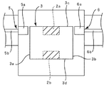
図1は、本発明とは異なるが、本発明の参考例に係るデュアルモード・バンドパスフィルタを説明するための斜視図であり、図2はその要部を模式的に示す平面図である。
デュアルモード・バンドパスフィルタ1は、矩形板状の誘電体基板2を有する。誘電体基板2の上面には、共振器を構成するためにCuからなる金属膜3が形成されている。金属膜3は、誘電体基板2上において部分的に形成されている。金属膜3は、本参考例では長方形の形状を有する。すなわち、金属膜3は、長手方向と短手方向とを有する形状である。
【0021】
本参考例では、金属膜3は、長辺の長さが1.6mm、短辺の長さが1.4mmとされている。
もっとも、金属膜3の寸法は、これに限定されず、所望とする中心周波数と帯域幅に応じて適宜変更し得る。
【0022】
誘電体基板2の上面においては、金属膜3に、短辺3a,3bと所定のギャップを隔てて入出力結合回路5,6が結合されている。入出力結合回路5,6は、金属膜3に結合される部分である入出力容量形成用パターン5a,6aと、入出力容量形成用パターン5a,6aに接続されたマイクロストリップライン5b,6bとを有する。
【0023】
なお、入出力結合回路5,6の金属膜3への結合点については異なる部分である限り図示の位置に限定されない。
誘電体基板2の下面には、全面にグラウンド電極4が形成されている。
【0024】
本参考例のバンドパスフィルタ1では、誘電体基板2が一様に構成されておらず、比誘電率が異なる誘電体基板層部分を有する。すなわち、金属膜3とグラウンド電極4とが誘電体基板2を対向している領域のうち、相対的に比誘電率が大きな部分2a,2bが形成されている。この比誘電率が大きな部分2a,2bは、本参考例では、比誘電率εr=17とされており、残りの誘電体基板部分の比誘電率がεr=7とされている。比誘電率の高い部分2a,2bは、長方形の金属膜3の長辺3c,3dの中央付近において、該長辺3c,3dに沿うように形成されている。また、比誘電率の高い部分2a,2bは、その平面形状が長方形であり、かつ誘電体基板2の厚み方向において、誘電体基板2の上面から下面に至るように形成されている。
【0025】
比誘電率の高い部分2a,2bと、残りの部分とを有するように誘電体基板2を構成する方法については特に限定されず、誘電体基板2を得た後に、誘電体基板部分2a,2bが設けられる部分に貫通孔を形成し、該貫通孔に比誘電率の高い誘電体材料を充填することにより形成することができる。あるいは、矩形の誘電体基板を得た後に、比誘電率の相対的に高い部分2a,2bに相当する部分に基板の構成材料と反応する元素を塗布し、熱拡散させることにより比誘電率の高い部分2a,2bを形成してもよい。
【0026】
本参考例では、誘電体基板2は、Mg、Si、Alなどの酸化物からなり、比誘電率の相対的に高い部分2a,2bは、Mg、Si、Alなどの酸化物に加えてCaあるいはTiの酸化物が付加されている。
【0027】
また、上記比誘電率の相対的に高い部分2a,2bの平面形状は長方形であるが、その短辺は200μm、長辺が600μmの寸法を有するように構成されている。
【0028】
本参考例のデュアルモード・バンドパスフィルタ1では、入出力結合回路5,6の一方とグラウンド電極4との間に入力電圧を印加することにより、入出力結合回路5,6の他方とグラウンド電極4との間で出力が取り出される。この場合、金属膜3が長方形の形状を有し、上記比誘電率の相対的に高い部分2a,2bが形成されているので、2つのモードの共振が結合され、デュアルモード・バンドパスフィルタとして動作する。これは、上記相対的に比誘電率の高い部分2a,2bが、金属膜3において生じる2つの共振を結合するように構成されているためである。これを、図3〜図7を参照して説明する。
【0029】
図3は、比較のために用意した共振器51を示す斜視図である。共振器51では、比誘電率の相対的に高い部分2a,2bが設けられていないことを除いては、上記参考例のデュアルモード・バンドパスフィルタ1と同様に構成されている。この共振器51の周波数特性を図4に示す。
【0030】
図4の実線A及び破線Bは、共振器51の反射特性及び通過特性をそれぞれ示す。
図4から明らかなように、矢印C,矢印Dで示す2つの共振が現れているものの、2つの共振が離れか周波数位置に現れており、結合されていない。共振器51では、金属膜3に結合されている入出力結合回路5,6の結合点を結ぶ方向と平行な方向、すなわち金属膜3の長辺方向に沿う共振と、該長辺と直交する方向すなわち短辺方向に沿う共振とが生じる。図4の矢印Cで示す共振は、上記長辺方向に沿う共振であり、矢印Dで示す共振は短辺方向に沿う共振である。
【0031】
図4から明らかなように、2つの共振は異なる周波数位置に現れており、結合していない。すなわち、バンドパスフィルタとして動作しない。
本願発明者らは、上記共振器51における共振電界を電磁界シュミレーター(ヒューレットパッカード社製、品番:HFSS)を用いて測定したところ、図5及び図6に示す結果が得られた。
【0032】
すなわち、共振Cでは、図5の破線Eで示す部分、すなわち長辺3c,3dの両側において短辺3a,3bに沿う部分が共振電界が強くなることが確かめられた。
【0033】
他方、短辺方向に沿う共振の場合には、図6に破線Fで示すように、金属膜3の長辺3c,3d近傍において共振電界が強くなることが確かめられた。
本願発明者らは、上記共振電界分布を考慮した結果、一方の共振に際しての共振電界を調整し、それによって共振C,共振Dの共振周波数を近づければ、バンドパスフィルタを構成し得ることを見い出した。
【0034】
上記参考例のデュアルモード・バンドパスフィルタ1では、上記のような知見のもとに、長辺3c,3dの略中央付近において、上記比誘電率の相対的に高い部分2a,2bを形成することにより、短辺方向に沿う共振、すなわち図4に示した共振Dの共振周波数を低下させ、2つの共振が結合されている。言い換えれば、2つの共振が結合するように、比誘電率の相対的に高い部分2a,2bが形成されている。
【0035】
図7に、本参考例のデュアルモード・バンドパスフィルタ1の周波数特性を示す。図7の実線Gが反射特性を、破線Hが通過特性を示す。また、比較のために、前述した共振器51の周波数特性も実線A及び破線Bで併せて示す。
【0036】
図7から明らかなように、本参考例のデュアルモード・バンドパスフィルタ1では、2つの共振が結合し、バンドパスフィルタとして動作し得ることがわかる。
【0037】
本参考例のデュアルモード・バンドパスフィルタ1では、上記比誘電率が相対的に高い部分2a,2bの残りの部分との比誘電率差、比誘電率が相対的に高い部分2a,2bの平面形状及び該平面形状の面積を調整することにより、短辺方向に伝搬する共振の共振周波数を容易に調整することかでき、それによって2つの共振を確実に結合することができるとともに、所望とする帯域幅のバンドパスフィルタ特性を容易に得ることができる。
【0038】
なお、上記参考例では、長辺側中央に比誘電率が相対的に高い部分2a,2bを設けたが、短辺側に比誘電率が残りの誘電体基板部分と異なる部分を設けてもよい。その場合には、長辺に沿って伝搬する共振の共振周波数が影響を受けることになるため、短辺側に比誘電率が異なる部分として、残りの部分に比べて比誘電率が相対的に低い部分を設ければよい。
【0039】
図8は、金属膜3の短辺3a,3b側に、比誘電率が相対的に低い部分が設けられた参考例の変形例を示す模式的平面図である。
本変形例のデュアルモード・バンドパスフィルタ11では、金属膜3の下方において、誘電体基板2に空洞2c,2dが設けられている。空洞2c,2dは、金属膜3とグラウンド電極とが対向されている領域において、金属膜3の短辺3a,3bに沿うように短辺略中央に設けられている。空洞2c,2dは、その平面形状が略長方形の形状とされており、該長方形の短辺が200μm、長辺が600μmの寸法を有する。また、空洞2c,2dは、誘電体基板2を上面から下面に貫くように形成されている。もっとも、空洞2c,2dは、必ずしも貫通する必要はない。
【0040】
空洞2c,2dにおける比誘電率は空気の比誘電率となるため、εr=1である。
本変形例のデュアルモード・バンドパスフィルタ11の周波数特性を図9に示す。図9において実線Iが反射特性を、破線Jが通過特性を示す。比較のために、前述した共振器51の周波数特性を併せて実線A及び破線Bで示す。
【0041】
図9から明らかなように、本変形例によれば、金属膜3の短辺側において上記空洞2c,2dが誘電体基板2に設けられているので、長辺方向に伝搬する共振の共振電界が影響を受け、共振Cの共振周波数が高められて、2つの共振が結合し、バンドパスフィルタとして動作することがわかる。
【0042】
図10及び図11は、本発明の実施例に係るバンドパスフィルタの要部を示す模式的平面図及び底面図である。本実施例のバンドパスフィルタ21では、誘電体基板22として、厚み300μmであり、比誘電率εr=7のMg、Si、Alの酸化物からなるものが用いられている。誘電体基板22の上面には、金属膜3及び入出力結合回路5,6が参考例と同様に構成されている。また、図11に示すように、誘電体基板2の下面にはグラウンド電極4が形成されている。本実施例の特徴は、グラウンド電極4において、貫通孔4a,4bが形成されていることにある。
【0043】
すなわち、貫通孔4a,4bは、金属膜3とグラウンド電極4とが対向している領域において、2つの共振を結合するように設けられている。本実施例では、貫通孔4a,4bは、金属膜3を下方に投影した場合の短辺3a,3bが位置している部分に沿うように、平面形状が長方形の貫通孔4a,4bが形成されている。
【0044】
従って、デュアルモード・バンドパスフィルタ21では、金属膜3の長辺方向に伝搬する共振の共振電界が強く現れる部分が貫通孔4a,4bにより影響を受け、図8に示した参考例の変形例と同様に、金属膜3の長辺方向に伝搬する共振Cの共振周波数が高められる。そして、貫通孔4a,4bが、上記共振Cと共振Dとが結合するように、その大きさが定められている。本実施例では、貫通孔4a,4bの一方が、長辺0.8mm、短辺0.4mmとされている。
【0045】
本実施例のデュアルモード・バンドパスフィルタ21の周波数特性を図12に実線K及び破線Lで示す。実線Kが反射特性を、破線Lが通過特性を示す。比較のために、共振器51の周波数特性を図12に併せて示す。図12から明らかなように、本実施例においても、貫通孔4a,4bの形成により2つの共振が結合されることがわかる。
【0046】
なお、参考例及び参考例の変形例では誘電体基板に、共振電界を制御するために比誘電率が残りの部分と異なる部分を設け、本実施例では、グラウンド電極に貫通孔を設けたが、これらの方法を併用してもよい。すなわち、参考例と本実施例とを組み合わせてもよい。
【0047】
また、実施例では、金属膜3は長方形の形状を有していたが、金属膜3の形状については特に限定されず、任意の形状とすることができる。もっとも、異なる共振周波数の2つの共振モードを発生させるには、長手方向と短手方向とを有する金属膜を用いることが望ましい。
【0048】
また、金属膜の具体的な平面形状としては、長方形、菱形、正多角形、円形または楕円形など様々な形状とすることができる。
また、実施例では、誘電体基板2の上面に金属膜3が形成されていたが、金属膜3は、誘電体基板のある高さ位置に形成されていもよい。同様に、グラウンド電極についても、金属膜3と誘電体基板層を介して対向され得る限り、誘電体基板2の下面に形成される必要は必ずしもなく、誘電体基板内に形成されていてもよい。
【0049】
さらに、誘電体基板2の中間高さ位置に金属膜を形成し、誘電体基板の上面及び下面にグラウンド電極を形成することにより、トリプレート構造を有するデュアルモード・バンドパスフィルタを構成してもよい。
【0050】
【発明の効果】
【0054】
本発明に係るデュアルモード・バンドパスフィルタでは、誘電体基板に共振器を構成するための金属膜が形成されており、該金属膜に入出力結合回路が結合されて共振周波数の異なる2つの共振モードが生じるように構成されている。そして、該2つの共振モードが結合するように、金属膜とグラウンド電極とが対向されている部分において、金属膜をグラウンド電極に投影した部分の外周に沿ってグラウンド電極に切欠が形成されている。従って、第1の発明と同様に、2つの共振モードが結合されて、デュアルモード・バンドパスフィルタとしての特性が得られる。
【0055】
共振器を構成する金属膜の形状や入出力結合回路の結合点の位置の制約がなく、従って、デュアルモード・バンドパスフィルタの設計の自由度を大幅に高め得る。
【0056】
しかも、上記グラウンド電極に設けられる貫通孔または切欠の形状、入出力結合回路の結合点の位置あるいは金属膜の寸法を変更することにより、帯域幅を大幅に調整することができる。
【0057】
よって、本発明によれば、所望とする帯域幅のデュアルモード・バンドパスフィルタを容易に提供することができる。
本発明において、誘電体基板の第1の主面に金属膜が形成されており、第2の主面にグラウンド電極が形成されている場合には、誘電体基板の両面に導電膜を形成することにより、本発明に係るデュアルモード・バンドパスフィルタを容易に構成することができる。
【0058】
上記金属膜が、長手方向と短手方向とを有する形状の場合には、共振周波数が異なる2つの共振モードを容易に発生させることができる。
もっとも、金属膜の平面形状は特に限定されないため、本発明では、様々な形状の金属膜を用いたデュアルモード・バンドパスフィルタを提供することができ、例えば、長方形、菱形、正多角形、円形または楕円形等の任意の形状とすることができる。
【図面の簡単な説明】
【図1】参考例のデュアルモード・バンドパスフィルタの斜視図。
【図2】参考例のデュアルモード・バンドパスフィルタの要部を示す模式的平面図。
【図3】比較のために用意した共振器を説明するための斜視図。
【図4】図3に示した共振器の周波数特性を示す図。
【図5】図3に示した共振器において、金属膜の長辺方向に沿う共振の際に共振電界が強く現れる部分を説明するための模式的平面図。
【図6】図3に示した共振器において、金属膜の短辺方向に沿う共振の際に共振電界が強く現れる部分を説明するための模式的平面図。
【図7】参考例及び比較のために用意した共振器の周波数特性を示す図。
【図8】参考例の変形例に係るデュアルモード・バンドパスフィルタを説明するための模式的平面図。
【図9】図8に示した変形例及び図3に示した共振器の周波数特性を示す図。
【図10】実施例に係るデュアルモード・バンドパスフィルタの要部を示す模式的平面図。
【図11】実施例のデュアルモード・バンドパスフィルタの底面図。
【図12】実施例のデュアルモード・バンドパスフィルタ及び比較のために用意した共振器の周波数特性を示す図。
【図13】従来のデュアルモード・バンドパスフィルタの一例を示す模式的平面図。
【図14】従来のデュアルモード・バンドパスフィルタの他の例を示す模式的平面図。
【図15】従来のデュアルモード・バンドパスフィルタのさらに他の例を示す模式的平面図。
【符号の説明】
1…デュアルモード・バンドパスフィルタ
2…誘電体基板
2a,2b…比誘電率が相対的に高い部分
2c,2d…空洞
3…共振器を構成する金属膜
3a,3b…短辺
3c,3d…長辺
4…グラウンド電極
4a,4b…貫通孔
5,6…入出力結合回路
11…デュアルモード・バンドパスフィルタ
21…デュアルモード・バンドパスフィルタ
22…誘電体基板[0001]
TECHNICAL FIELD OF THE INVENTION
The present invention relates to a dual-mode bandpass filter used as a bandpass filter in, for example, a communication device in a microwave to millimeter wave band.
[0002]
[Prior art]
2. Description of the Related Art Conventionally, various types of dual-mode bandpass filters have been proposed as bandpass filters used in a high-frequency region (for example, MINIATURE DUAL MODE MICROSTRIP FILTERS, JA Curtis and SJ Fiedziszko, 1991 IEEE MTT-S Digest, etc.). ).
[0003]
FIGS. 13 and 14 are schematic plan views illustrating a conventional dual-mode bandpass filter.
In the
[0004]
On the other hand, a dual mode filter using an annular conductive film instead of a circular conductive film has also been proposed (Japanese Patent Application Laid-Open Nos. 9-139612 and 9-162610). That is, similarly to the dual mode bandpass filter shown in FIG. 13, the input / output coupling circuit is arranged so as to form a central angle of 90 ° using an annular ring transmission line, and the ring transmission line A dual mode filter in which an open-end stub is provided in part is disclosed.
[0005]
Japanese Patent Application Laid-Open No. Hei 6-112701 discloses a dual mode filter using a similar ring transmission line. As shown in FIG. 15, in the
[0006]
It is described that with the above configuration, it is possible to generate quadrature mode resonance that is not coupled to each other in the ring resonator composed of one strip line, and to control the degree of coupling by the
[0007]
[Problems to be solved by the invention]
In the conventional dual-mode bandpass filter shown in FIGS. 13 and 14, a two-stage bandpass filter can be formed by forming one conductive film pattern, and thus the bandpass filter can be downsized. obtain.
[0008]
However, in the circular or square conductive film pattern, the input / output coupling circuit is configured to be coupled at the above-described specific angle, so that the degree of coupling cannot be increased and a wide pass band cannot be obtained. was there.
[0009]
Further, in the band-pass filter shown in FIG. 13, the
[0010]
Also, in a dual mode bandpass filter using a ring resonator as described in JP-A-9-139612 and JP-A-9-162610, it is similarly difficult to increase the degree of coupling. In addition, there is a problem that the shape of the ring-shaped resonator is limited.
[0011]
On the other hand, in the
[0012]
An object of the present invention is to solve the above-mentioned disadvantages of the prior art, not only to achieve downsizing, but also to increase the degree of coupling, to easily adjust the degree of coupling, and to easily widen the pass band. It is another object of the present invention to provide a dual-mode bandpass filter which can be realized and has excellent design flexibility.
[0013]
[Means for Solving the Problems]
[0015]
According to a broad aspect of the present invention, a dielectric substrate having first and second main surfaces and a portion formed at a first main surface of the dielectric substrate or at a certain height position of the dielectric substrate A metal film, at least one ground electrode formed in the second main surface of the dielectric substrate or in the dielectric substrate so as to face the metal film via the dielectric substrate layer, A pair of input / output coupling circuits coupled by a portion, and in the portion where the metal film and the ground electrode face each other, such that two resonance modes having different resonance frequencies are generated in the metal film. A dual mode bandpass filter is provided, wherein a through hole or a notch is formed in the ground electrode along an outer periphery of a portion where the metal film is projected on the ground electrode.
[0016]
In this onset bright, as the two resonant modes are coupled, in a portion where the metal film and the ground electrode are opposite, the through hole or notch in the ground electrode is formed. That is, a resonance mode propagates in two directions: a direction substantially parallel to the lower layer line connecting the pair of input / output coupling circuits to the metal film and a direction orthogonal to the lower layer line. The resonance frequency fluctuates under the influence of the through hole or the notch. That is, the through hole or notch is formed so as to influence the resonance electric field or resonance current of one resonance mode so as to couple one resonance mode with the other resonance mode. Therefore, the two resonance modes are coupled by the through hole or the notch and operate as a dual mode bandpass filter.
[0017]
In a specific aspect of the present invention, a metal film is formed on a first main surface of the dielectric substrate, and a ground electrode is formed on a second main surface.
In still another specific aspect of the dual mode bandpass filter according to the present invention, the metal film has a shape having a longitudinal direction and a lateral direction.
[0018]
In yet another specific aspect of the present invention, the planar shape of the metal film is a rectangle, a rhombus, a regular polygon, a circle, or an ellipse.
[0019]
BEST MODE FOR CARRYING OUT THE INVENTION
Hereinafter, the present invention will be clarified by describing specific examples of the present invention.
[0020]
FIG. 1 is a perspective view for explaining a dual mode bandpass filter according to a reference example of the present invention, which is different from the present invention , and FIG. 2 is a plan view schematically showing a main part thereof.
The dual-mode bandpass filter 1 has a rectangular plate-shaped
[0021]
In this reference example, the length of the long side of the
However, the size of the
[0022]
On the upper surface of the
[0023]
The connection points of the input /
A
[0024]
In the band-pass filter 1 of the present reference example, the
[0025]
The method of forming the
[0026]
In the present reference example, the
[0027]
The planar shapes of the relatively high
[0028]
In the dual mode bandpass filter 1 of the present reference example, an input voltage is applied between one of the input /
[0029]
FIG. 3 is a perspective view showing the
[0030]
4 indicate the reflection characteristics and the transmission characteristics of the
As is apparent from FIG. 4, two resonances indicated by arrows C and D appear, but the two resonances appear separately or at a frequency position and are not coupled. In the
[0031]
As is evident from FIG. 4, the two resonances appear at different frequency positions and are not coupled. That is, it does not operate as a bandpass filter.
The present inventors measured the resonance electric field in the
[0032]
That is, in the resonance C, it was confirmed that the portion indicated by the broken line E in FIG. 5, that is, the portion along the
[0033]
On the other hand, in the case of resonance along the short side direction, it was confirmed that the resonance electric field becomes strong near the
The inventors of the present invention have considered that as a result of considering the above-described resonance electric field distribution, a band-pass filter can be formed by adjusting the resonance electric field at the time of one resonance and thereby bringing the resonance frequencies of the resonance C and the resonance D closer to each other. I found it.
[0034]
In the dual mode bandpass filter 1 of the above-described reference example, the
[0035]
FIG. 7 shows frequency characteristics of the dual mode bandpass filter 1 of the present reference example. The solid line G in FIG. 7 indicates the reflection characteristic, and the broken line H indicates the transmission characteristic. For comparison, the solid line A and the broken line B also show the frequency characteristics of the
[0036]
As is clear from FIG. 7, in the dual mode bandpass filter 1 of the present reference example, two resonances are coupled, and it is possible to operate as a bandpass filter.
[0037]
In the dual mode bandpass filter 1 of the present reference example, the relative permittivity difference between the
[0038]
In the above reference example, the
[0039]
FIG. 8 is a schematic plan view showing a modification of the reference example in which a portion having a relatively low relative dielectric constant is provided on the
In the dual
[0040]
Since the relative dielectric constant of the
FIG. 9 shows the frequency characteristics of the dual
[0041]
As is clear from FIG. 9, according to the present modification, since the
[0042]
10 and 11 are schematic plan view and a bottom view showing the main part of the band-pass filter according to the actual施例of the present invention. In the band-
[0043]
That is, the through
[0044]
Therefore, in the dual mode band-
[0045]
The frequency characteristics of the dual
[0046]
In the reference example and the modification of the reference example, a portion having a relative permittivity different from that of the remaining portion is provided on the dielectric substrate to control the resonance electric field. In the present embodiment, the through-hole is provided in the ground electrode. These methods may be used in combination. That is, the reference example and the present embodiment may be combined.
[0047]
Further, in the real施例, the
[0048]
Further, a specific planar shape of the metal film can be various shapes such as a rectangle, a rhombus, a regular polygon, a circle, or an ellipse.
Also, in the real施例, the
[0049]
Further, a dual mode bandpass filter having a triplate structure may be formed by forming a metal film at an intermediate height position of the
[0050]
【The invention's effect】
[0054]
In the dual mode band-pass filter according to the present invention, a metal film for forming a resonator is formed on a dielectric substrate, and an input / output coupling circuit is coupled to the metal film to form two resonators having different resonance frequencies. The mode is configured to occur. A notch is formed in the ground electrode along the outer periphery of the portion where the metal film is projected on the ground electrode at a portion where the metal film and the ground electrode face each other so that the two resonance modes are coupled. . Therefore, as in the first aspect, the two resonance modes are coupled, and a characteristic as a dual mode bandpass filter is obtained.
[0055]
No restriction of the position of the point of attachment of the shape and input-output coupling circuits of the metal film constituting the co-acoustic transducer, and thus may greatly increase the degree of freedom in design of the dual-mode bandpass filter.
[0056]
Moreover, the bandwidth can be largely adjusted by changing the shape of the through hole or notch provided in the ground electrode, the position of the coupling point of the input / output coupling circuit, or the size of the metal film.
[0057]
Therefore, according to the present invention, it is possible to easily provide a dual-mode bandpass filter having a desired bandwidth.
In the present invention, when a metal film is formed on a first main surface of a dielectric substrate and a ground electrode is formed on a second main surface, conductive films are formed on both surfaces of the dielectric substrate. Thus, the dual mode bandpass filter according to the present invention can be easily configured.
[0058]
When the metal film has a shape having a longitudinal direction and a lateral direction, two resonance modes having different resonance frequencies can be easily generated.
However, since the planar shape of the metal film is not particularly limited, the present invention can provide a dual mode bandpass filter using various shapes of metal films, for example, a rectangle, a rhombus, a regular polygon, and a circle. Alternatively, the shape can be an arbitrary shape such as an ellipse.
[Brief description of the drawings]
FIG. 1 is a perspective view of a dual mode bandpass filter of a reference example.
FIG. 2 is a schematic plan view showing a main part of a dual mode bandpass filter of a reference example.
FIG. 3 is a perspective view for explaining a resonator prepared for comparison.
FIG. 4 is a view showing frequency characteristics of the resonator shown in FIG. 3;
FIG. 5 is a schematic plan view for explaining a portion where a resonance electric field appears strongly during resonance along a long side direction of the metal film in the resonator shown in FIG. 3;
FIG. 6 is a schematic plan view for explaining a portion where a resonance electric field strongly appears at the time of resonance along the short side direction of the metal film in the resonator shown in FIG. 3;
FIG. 7 is a diagram showing frequency characteristics of a reference example and a resonator prepared for comparison.
FIG. 8 is a schematic plan view for explaining a dual mode bandpass filter according to a modification of the reference example.
FIG. 9 is a diagram illustrating frequency characteristics of the modification illustrated in FIG. 8 and the resonator illustrated in FIG. 3;
Figure 10 is a schematic plan view showing a main part of the dual-mode bandpass filter according to the actual施例.
FIG. 11 is a bottom view of the dual-mode band pass filter of the real施例.
Diagram showing the frequency characteristic of the resonator prepared for the 12 dual-mode bandpass filter and compare actual施例.
FIG. 13 is a schematic plan view showing an example of a conventional dual mode bandpass filter.
FIG. 14 is a schematic plan view showing another example of a conventional dual mode bandpass filter.
FIG. 15 is a schematic plan view showing still another example of a conventional dual mode bandpass filter.
[Explanation of symbols]
DESCRIPTION OF SYMBOLS 1 ... Dual mode
Claims (4)
前記誘電体基板の第1の主面または誘電体基板のある高さ位置において部分的に形成された金属膜と、
前記金属膜と誘電体基板層を介して対向するように、誘電体基板の第2の主面または誘電体基板内に形成された少なくとも1つのグラウンド電極と、
前記金属膜に異なる部分で結合された一対の入出力結合回路とを備え、
前記金属膜において生じる、共振周波数の異なる2つの共振モードが結合するように、前記金属膜とグラウンド電極とが対向されている部分において、金属膜をグラウンド電極に投影した部分の外周に沿って前記グラウンド電極に貫通孔または切欠が形成されていることを特徴とする、デュアルモード・バンドパスフィルタ。A dielectric substrate having first and second main surfaces;
A metal film partially formed at a first principal surface of the dielectric substrate or at a certain height position of the dielectric substrate;
At least one ground electrode formed in the second main surface of the dielectric substrate or in the dielectric substrate so as to face the metal film via the dielectric substrate layer;
A pair of input / output coupling circuits coupled to the metal film at different portions,
In the portion where the metal film and the ground electrode are opposed to each other, the two resonance modes having different resonance frequencies generated in the metal film are coupled along the outer periphery of the portion where the metal film is projected on the ground electrode. A dual-mode bandpass filter, wherein a through hole or a notch is formed in a ground electrode.
Priority Applications (6)
| Application Number | Priority Date | Filing Date | Title |
|---|---|---|---|
| JP2000151756A JP3562442B2 (en) | 2000-05-23 | 2000-05-23 | Dual-mode bandpass filter |
| EP01111072A EP1170819B1 (en) | 2000-05-23 | 2001-05-08 | Dual mode band pass filter |
| EP03019351A EP1396904A3 (en) | 2000-05-23 | 2001-05-08 | Dual mode band pass filter |
| DE60109001T DE60109001T2 (en) | 2000-05-23 | 2001-05-08 | Dual mode bandpass filter |
| US09/855,298 US6556109B2 (en) | 2000-05-23 | 2001-05-15 | Dual mode band pass filter |
| KR10-2001-0028464A KR100397733B1 (en) | 2000-05-23 | 2001-05-23 | Dual mode band pass filter |
Applications Claiming Priority (1)
| Application Number | Priority Date | Filing Date | Title |
|---|---|---|---|
| JP2000151756A JP3562442B2 (en) | 2000-05-23 | 2000-05-23 | Dual-mode bandpass filter |
Publications (2)
| Publication Number | Publication Date |
|---|---|
| JP2001332905A JP2001332905A (en) | 2001-11-30 |
| JP3562442B2 true JP3562442B2 (en) | 2004-09-08 |
Family
ID=18657260
Family Applications (1)
| Application Number | Title | Priority Date | Filing Date |
|---|---|---|---|
| JP2000151756A Expired - Fee Related JP3562442B2 (en) | 2000-05-23 | 2000-05-23 | Dual-mode bandpass filter |
Country Status (5)
| Country | Link |
|---|---|
| US (1) | US6556109B2 (en) |
| EP (2) | EP1396904A3 (en) |
| JP (1) | JP3562442B2 (en) |
| KR (1) | KR100397733B1 (en) |
| DE (1) | DE60109001T2 (en) |
Families Citing this family (9)
| Publication number | Priority date | Publication date | Assignee | Title |
|---|---|---|---|---|
| EP1223591A3 (en) * | 2001-01-11 | 2007-06-06 | Matsushita Electric Industrial Co., Ltd. | Multilayer electronic component and communication apparatus |
| US6825740B2 (en) * | 2002-02-08 | 2004-11-30 | Tdk Corporation | TEM dual-mode rectangular dielectric waveguide bandpass filter |
| US6963259B2 (en) * | 2002-06-27 | 2005-11-08 | Harris Corporation | High efficiency resonant line |
| US6727785B2 (en) * | 2002-06-27 | 2004-04-27 | Harris Corporation | High efficiency single port resonant line |
| US6903634B2 (en) * | 2002-11-12 | 2005-06-07 | Silicon Integrated Systems Corp. | Method of detuning resonant frequencies of a power distribution system |
| JP5029519B2 (en) * | 2008-07-08 | 2012-09-19 | 富士通株式会社 | filter |
| TWI381574B (en) * | 2008-09-24 | 2013-01-01 | Univ Nat Changhua Education | Dual band bandpass filter |
| JP5120278B2 (en) * | 2009-01-26 | 2013-01-16 | 富士通株式会社 | Superconducting tunable filter device, nonlinear strain measuring device, nonlinear strain measuring method |
| US9490768B2 (en) * | 2012-06-25 | 2016-11-08 | Knowles Cazenovia Inc. | High frequency band pass filter with coupled surface mount transition |
Family Cites Families (12)
| Publication number | Priority date | Publication date | Assignee | Title |
|---|---|---|---|---|
| US4488131A (en) * | 1983-02-25 | 1984-12-11 | Hughes Aircraft Company | MIC Dual mode ring resonator filter |
| US5136268A (en) * | 1991-04-19 | 1992-08-04 | Space Systems/Loral, Inc. | Miniature dual mode planar filters |
| JP2906863B2 (en) | 1992-09-28 | 1999-06-21 | 松下電器産業株式会社 | Stripline dual mode filter |
| EP0755577A1 (en) * | 1994-04-14 | 1997-01-29 | E.I. Du Pont De Nemours And Company | High power high-temperature superconductive filters |
| GB9426294D0 (en) * | 1994-12-28 | 1995-02-22 | Mansour Raafat | High power soperconductive circuits and method of construction thereof |
| JPH08204437A (en) * | 1995-01-30 | 1996-08-09 | Matsushita Electric Works Ltd | Method for adjusting resonance frequency for microstrip antenna |
| US5750473A (en) * | 1995-05-11 | 1998-05-12 | E. I. Du Pont De Nemours And Company | Planar high temperature superconductor filters with backside coupling |
| JP3304724B2 (en) | 1995-11-16 | 2002-07-22 | 松下電器産業株式会社 | Dual mode filter |
| JPH09162610A (en) | 1995-12-14 | 1997-06-20 | Matsushita Electric Ind Co Ltd | Dual mode resonator |
| US5751201A (en) * | 1996-06-19 | 1998-05-12 | Motorola, Inc. | Resonator with metal layers devoid of DC connection and semiconductor device in substrate |
| JP3277834B2 (en) * | 1996-12-11 | 2002-04-22 | 松下電器産業株式会社 | Planar bandpass filter |
| JPH11122032A (en) * | 1997-10-11 | 1999-04-30 | Yokowo Co Ltd | Microstrip antenna |
-
2000
- 2000-05-23 JP JP2000151756A patent/JP3562442B2/en not_active Expired - Fee Related
-
2001
- 2001-05-08 DE DE60109001T patent/DE60109001T2/en not_active Expired - Lifetime
- 2001-05-08 EP EP03019351A patent/EP1396904A3/en not_active Withdrawn
- 2001-05-08 EP EP01111072A patent/EP1170819B1/en not_active Expired - Lifetime
- 2001-05-15 US US09/855,298 patent/US6556109B2/en not_active Expired - Fee Related
- 2001-05-23 KR KR10-2001-0028464A patent/KR100397733B1/en not_active IP Right Cessation
Also Published As
| Publication number | Publication date |
|---|---|
| KR20010107691A (en) | 2001-12-07 |
| US6556109B2 (en) | 2003-04-29 |
| DE60109001D1 (en) | 2005-03-31 |
| EP1170819A2 (en) | 2002-01-09 |
| JP2001332905A (en) | 2001-11-30 |
| EP1170819B1 (en) | 2005-02-23 |
| US20020039059A1 (en) | 2002-04-04 |
| DE60109001T2 (en) | 2006-02-09 |
| EP1396904A2 (en) | 2004-03-10 |
| EP1396904A3 (en) | 2005-11-30 |
| KR100397733B1 (en) | 2003-09-13 |
| EP1170819A3 (en) | 2002-01-16 |
Similar Documents
| Publication | Publication Date | Title |
|---|---|---|
| US7239221B2 (en) | Dual mode band-pass filter | |
| JP3562442B2 (en) | Dual-mode bandpass filter | |
| JP3575378B2 (en) | Frequency adjustment method of attenuation pole of dual mode bandpass filter | |
| JP3587139B2 (en) | Dual-mode bandpass filter | |
| JP3804481B2 (en) | Dual mode bandpass filter, duplexer, and wireless communication device | |
| JP4438253B2 (en) | Bandpass filter characteristics adjustment method | |
| JP2004320351A (en) | Dual-mode band pass filter, duplexer and radio communication equipment | |
| JP4442066B2 (en) | Dual-mode bandpass filter, characteristic adjustment method for dual-mode bandpass filter, duplexer, and wireless communication apparatus | |
| JP2004349960A (en) | Band-pass filter | |
| JP2004312184A (en) | Dual mode band-pass filter, duplexer and radio communication apparatus | |
| JP2001320204A (en) | Dual mode band pass filter | |
| JP2000134004A (en) | Dielectric filter | |
| JP2002261508A (en) | Dual mode bandpass filter and duplexer and radio communication device | |
| JPH11330817A (en) | Dielectric resonator device, dielectric filter, oscillator and electronic equipment | |
| JPH05327312A (en) | Dielectric filter |
Legal Events
| Date | Code | Title | Description |
|---|---|---|---|
| A131 | Notification of reasons for refusal |
Free format text: JAPANESE INTERMEDIATE CODE: A131 Effective date: 20040127 |
|
| A521 | Request for written amendment filed |
Free format text: JAPANESE INTERMEDIATE CODE: A523 Effective date: 20040324 |
|
| TRDD | Decision of grant or rejection written | ||
| A01 | Written decision to grant a patent or to grant a registration (utility model) |
Free format text: JAPANESE INTERMEDIATE CODE: A01 Effective date: 20040511 |
|
| A61 | First payment of annual fees (during grant procedure) |
Free format text: JAPANESE INTERMEDIATE CODE: A61 Effective date: 20040524 |
|
| R150 | Certificate of patent or registration of utility model |
Free format text: JAPANESE INTERMEDIATE CODE: R150 |
|
| FPAY | Renewal fee payment (event date is renewal date of database) |
Free format text: PAYMENT UNTIL: 20080611 Year of fee payment: 4 |
|
| FPAY | Renewal fee payment (event date is renewal date of database) |
Free format text: PAYMENT UNTIL: 20090611 Year of fee payment: 5 |
|
| FPAY | Renewal fee payment (event date is renewal date of database) |
Free format text: PAYMENT UNTIL: 20090611 Year of fee payment: 5 |
|
| FPAY | Renewal fee payment (event date is renewal date of database) |
Free format text: PAYMENT UNTIL: 20100611 Year of fee payment: 6 |
|
| FPAY | Renewal fee payment (event date is renewal date of database) |
Free format text: PAYMENT UNTIL: 20110611 Year of fee payment: 7 |
|
| FPAY | Renewal fee payment (event date is renewal date of database) |
Free format text: PAYMENT UNTIL: 20120611 Year of fee payment: 8 |
|
| FPAY | Renewal fee payment (event date is renewal date of database) |
Free format text: PAYMENT UNTIL: 20130611 Year of fee payment: 9 |
|
| LAPS | Cancellation because of no payment of annual fees |