JP3553361B2 - Optical amplifier dynamic gain control system and method - Google Patents
Optical amplifier dynamic gain control system and method Download PDFInfo
- Publication number
- JP3553361B2 JP3553361B2 JP08059598A JP8059598A JP3553361B2 JP 3553361 B2 JP3553361 B2 JP 3553361B2 JP 08059598 A JP08059598 A JP 08059598A JP 8059598 A JP8059598 A JP 8059598A JP 3553361 B2 JP3553361 B2 JP 3553361B2
- Authority
- JP
- Japan
- Prior art keywords
- pump
- power
- gain
- channel
- input
- Prior art date
- Legal status (The legal status is an assumption and is not a legal conclusion. Google has not performed a legal analysis and makes no representation as to the accuracy of the status listed.)
- Expired - Fee Related
Links
Images


Classifications
-
- H—ELECTRICITY
- H04—ELECTRIC COMMUNICATION TECHNIQUE
- H04B—TRANSMISSION
- H04B10/00—Transmission systems employing electromagnetic waves other than radio-waves, e.g. infrared, visible or ultraviolet light, or employing corpuscular radiation, e.g. quantum communication
- H04B10/29—Repeaters
- H04B10/291—Repeaters in which processing or amplification is carried out without conversion of the main signal from optical form
- H04B10/293—Signal power control
- H04B10/294—Signal power control in a multiwavelength system, e.g. gain equalisation
- H04B10/2942—Signal power control in a multiwavelength system, e.g. gain equalisation using automatic gain control [AGC]
-
- H—ELECTRICITY
- H01—ELECTRIC ELEMENTS
- H01S—DEVICES USING THE PROCESS OF LIGHT AMPLIFICATION BY STIMULATED EMISSION OF RADIATION [LASER] TO AMPLIFY OR GENERATE LIGHT; DEVICES USING STIMULATED EMISSION OF ELECTROMAGNETIC RADIATION IN WAVE RANGES OTHER THAN OPTICAL
- H01S3/00—Lasers, i.e. devices using stimulated emission of electromagnetic radiation in the infrared, visible or ultraviolet wave range
- H01S3/10—Controlling the intensity, frequency, phase, polarisation or direction of the emitted radiation, e.g. switching, gating, modulating or demodulating
- H01S3/13—Stabilisation of laser output parameters, e.g. frequency or amplitude
- H01S3/1301—Stabilisation of laser output parameters, e.g. frequency or amplitude in optical amplifiers
- H01S3/13013—Stabilisation of laser output parameters, e.g. frequency or amplitude in optical amplifiers by controlling the optical pumping
-
- H—ELECTRICITY
- H04—ELECTRIC COMMUNICATION TECHNIQUE
- H04B—TRANSMISSION
- H04B10/00—Transmission systems employing electromagnetic waves other than radio-waves, e.g. infrared, visible or ultraviolet light, or employing corpuscular radiation, e.g. quantum communication
- H04B10/29—Repeaters
- H04B10/291—Repeaters in which processing or amplification is carried out without conversion of the main signal from optical form
- H04B10/2912—Repeaters in which processing or amplification is carried out without conversion of the main signal from optical form characterised by the medium used for amplification or processing
-
- H—ELECTRICITY
- H04—ELECTRIC COMMUNICATION TECHNIQUE
- H04B—TRANSMISSION
- H04B10/00—Transmission systems employing electromagnetic waves other than radio-waves, e.g. infrared, visible or ultraviolet light, or employing corpuscular radiation, e.g. quantum communication
- H04B10/29—Repeaters
- H04B10/291—Repeaters in which processing or amplification is carried out without conversion of the main signal from optical form
- H04B10/293—Signal power control
- H04B10/294—Signal power control in a multiwavelength system, e.g. gain equalisation
- H04B10/296—Transient power control, e.g. due to channel add/drop or rapid fluctuations in the input power
-
- H—ELECTRICITY
- H01—ELECTRIC ELEMENTS
- H01S—DEVICES USING THE PROCESS OF LIGHT AMPLIFICATION BY STIMULATED EMISSION OF RADIATION [LASER] TO AMPLIFY OR GENERATE LIGHT; DEVICES USING STIMULATED EMISSION OF ELECTROMAGNETIC RADIATION IN WAVE RANGES OTHER THAN OPTICAL
- H01S3/00—Lasers, i.e. devices using stimulated emission of electromagnetic radiation in the infrared, visible or ultraviolet wave range
- H01S3/05—Construction or shape of optical resonators; Accommodation of active medium therein; Shape of active medium
- H01S3/06—Construction or shape of active medium
- H01S3/063—Waveguide lasers, i.e. whereby the dimensions of the waveguide are of the order of the light wavelength
- H01S3/067—Fibre lasers
- H01S3/06754—Fibre amplifiers
-
- H—ELECTRICITY
- H01—ELECTRIC ELEMENTS
- H01S—DEVICES USING THE PROCESS OF LIGHT AMPLIFICATION BY STIMULATED EMISSION OF RADIATION [LASER] TO AMPLIFY OR GENERATE LIGHT; DEVICES USING STIMULATED EMISSION OF ELECTROMAGNETIC RADIATION IN WAVE RANGES OTHER THAN OPTICAL
- H01S3/00—Lasers, i.e. devices using stimulated emission of electromagnetic radiation in the infrared, visible or ultraviolet wave range
- H01S3/09—Processes or apparatus for excitation, e.g. pumping
- H01S3/091—Processes or apparatus for excitation, e.g. pumping using optical pumping
- H01S3/094—Processes or apparatus for excitation, e.g. pumping using optical pumping by coherent light
- H01S3/0941—Processes or apparatus for excitation, e.g. pumping using optical pumping by coherent light of a laser diode
- H01S3/09415—Processes or apparatus for excitation, e.g. pumping using optical pumping by coherent light of a laser diode the pumping beam being parallel to the lasing mode of the pumped medium, e.g. end-pumping
-
- H—ELECTRICITY
- H01—ELECTRIC ELEMENTS
- H01S—DEVICES USING THE PROCESS OF LIGHT AMPLIFICATION BY STIMULATED EMISSION OF RADIATION [LASER] TO AMPLIFY OR GENERATE LIGHT; DEVICES USING STIMULATED EMISSION OF ELECTROMAGNETIC RADIATION IN WAVE RANGES OTHER THAN OPTICAL
- H01S3/00—Lasers, i.e. devices using stimulated emission of electromagnetic radiation in the infrared, visible or ultraviolet wave range
- H01S3/10—Controlling the intensity, frequency, phase, polarisation or direction of the emitted radiation, e.g. switching, gating, modulating or demodulating
- H01S3/13—Stabilisation of laser output parameters, e.g. frequency or amplitude
- H01S3/1305—Feedback control systems
-
- H—ELECTRICITY
- H01—ELECTRIC ELEMENTS
- H01S—DEVICES USING THE PROCESS OF LIGHT AMPLIFICATION BY STIMULATED EMISSION OF RADIATION [LASER] TO AMPLIFY OR GENERATE LIGHT; DEVICES USING STIMULATED EMISSION OF ELECTROMAGNETIC RADIATION IN WAVE RANGES OTHER THAN OPTICAL
- H01S5/00—Semiconductor lasers
- H01S5/06—Arrangements for controlling the laser output parameters, e.g. by operating on the active medium
- H01S5/068—Stabilisation of laser output parameters
- H01S5/0683—Stabilisation of laser output parameters by monitoring the optical output parameters
-
- H—ELECTRICITY
- H01—ELECTRIC ELEMENTS
- H01S—DEVICES USING THE PROCESS OF LIGHT AMPLIFICATION BY STIMULATED EMISSION OF RADIATION [LASER] TO AMPLIFY OR GENERATE LIGHT; DEVICES USING STIMULATED EMISSION OF ELECTROMAGNETIC RADIATION IN WAVE RANGES OTHER THAN OPTICAL
- H01S5/00—Semiconductor lasers
- H01S5/10—Construction or shape of the optical resonator, e.g. extended or external cavity, coupled cavities, bent-guide, varying width, thickness or composition of the active region
- H01S5/14—External cavity lasers
- H01S5/141—External cavity lasers using a wavelength selective device, e.g. a grating or etalon
Landscapes
- Physics & Mathematics (AREA)
- Electromagnetism (AREA)
- Engineering & Computer Science (AREA)
- Computer Networks & Wireless Communication (AREA)
- Signal Processing (AREA)
- Plasma & Fusion (AREA)
- Optics & Photonics (AREA)
- Lasers (AREA)
- Optical Communication System (AREA)
Description
【0001】
【発明の属する技術分野】
本発明は、光通信システムに関し、特に、光増幅器の動的ゲイン制御システムに関するものである。
【0002】
【従来の技術】
光通信システムは、情報信号チャネルに広帯域が利用できるので望ましい。光送信器および受信器の速度制限によって、単一の波長を使用している間は、この広帯域を十分に活用することが難しくなる。従って、大容量の光送信システムは、概して、高速システムを波長分割多重(WDM)によって単一のファイバ上に結合させることにより、利用可能な帯域を全て使用することになる。このようなWDM光送信システムは、概して、稀土類ドープファイバ光増幅器(例えば、エルビウムやエルビウム−イッテルビイウムがドープされたもの)が使用され、ファイバリンクや分割損失を補う。光増幅器は、特定の条件下において、システムに好ましくないノイズを加える。さらに、稀土類ドープファイバ増幅器は、いくつかの適用において、課題が残されている。
【0003】
光増幅器のゲイン過渡は、波長分割多重(WDM)光システムにとって大きな問題である。このシステムでは、ネットワークの再構成あるいは障害によって、チャネルが追加または減少する。チャネルの追加により、現在のチャネルのパワーが弱まり、受信器が感知できなくなる。チャネルの減少により、残存チャネルのパワーが非線形効果の閾値を越えるために、好ましくない反射やノイズを引き起こす誘導ブリュアン散乱(SBS)やチャネル間のクロストークを追加する4光波混合(FWM)など、残存チャネルにエラーが起こりやすくなる。これらパワー過渡の結果として起こる残存チャネルあるいは現在チャネルにおけるエラーバーストは、サービス提供者にとって受け入れられないものである。
【0004】
さらに、エルビウムドープファイバ増幅器においては、光波長にわたりゲインが統一されていない。これは、エルビウムドープ増幅器のゲインが、ファイバ内エルビウムイオンの吸収/発散波長スペクトルによって固有に判定されるためである。これは、多重波長が同時に増幅されるWDMシステムにとって重大な問題となる。このため、比較的一定した多チャネルゲインを有し、WDM重力チャネルの数、パワー、波長、変調方法の変化に関わらず、WDMチャネル間のゲイン変動が少ないエルビウムドープファイバ増幅器(EDFA)が求められる。エルビウムドープファイバ(EDF)には、反転レベルが存在し、このため、多チャネルゲインに多少の変動が起こる。反転レベルは、ファイバ内の全体のエルビウムイオンのうち、反転あるいは励起したエルビウムイオンの数をいう。理想的なバージョンのEDFAについては、WDMチャネル間のゲイン変動がゼロである。実際、EDFAのうち多チャネルゲイン変動が低いものでも、チャネル間に多少(例えば1dB)のチャネルゲイン変動が依然として起こり、これを受動光フィルタの使用により減少させ、それによって、比較的平坦で一定したEDFAの多チャネルゲインvと波長スペクトルが、EDFAの作動波長域内で得られる。
【0005】
光増幅器とその応用についての1996年会議、OAA’96のテクニカルダイジェストであるPostdeadline Paper PDP4のA.K.Srivastava他による「エルビウムドープファイバ増幅器の第一ゲイン制御」によれば、出力パワー制御システムは、チャネルから出力パワーを量り、フィードバック・ループとともにポンプレーザを駆動させることによって、チャネルの出力パワーを比較的一定に保っている。しかしながら、このシステムでは、本当のゲイン制御を得ることはできない。なぜならば、ゲイン制御は、一定の入力パワーである時のみ得られるものである。この解決策の短所は、出力パワーの測定に使用されるチャネルそのものが減少された場合、作動しなくなることである。さらに上述したように、このシステムでは、測定されたチャネルの入力パワーが変化したときに、多チャネルゲインおよび多チャネルゲインスペクトルの非変動が維持できない。
【0006】
カリフォルニア、サンノゼにおける1993年、光ファイバ通信会議(OFC’93)の論文Tu15(第40〜42頁)のK.Motoshima他による「エルビウムドープファイバ増幅器におけるポンプフィードバック制御による過渡ゲイン飽和の動的補完」によれば、システムは、余分のプローブ信号を有しており、その信号の波長はEDFAのゲイン波長域に位置づけられるが、可能な信号波長には存在せず、それによりゲインを測定し安定させている。そして、プローブ信号の入力パワー、出力パワーのいずれもが測定され、実際のゲインが決定される。フィードバック回路を使用して、ポンプレーザダイオード電流とそのパワーを供給することにより、システムは比較的変化のないゲインを生成する。この技術の短所は、プローブ信号供給のための余分のDFBレーザと、プローブ信号を追加し抽出するための鋭角波長多重器が、全てのEDFAに必要とされることであり、EDFAの製造コストが増加する。
【0007】
光増幅器とその応用についての1996年会議、OAA’96のテクニカルダイジェストであるPaper FB2(第77〜80頁)のJ.Massicott他による「全光ゲイン制御のエルビウムドープファイバ増幅器の低ノイズ動作を達成する非対称制御レーザキャビティ」によれば、光ゲインのクランプによる解決策が報告されている。しかし、光ゲインのクランプ使用は、余分な信号波長光反射器が少なくとも2つは必要となる。さらに、ゲインクランプ制御のためのフィルタおよび/または反射器により、信号波長に追加的損失が起こるため、使用可能なポンプパワーでは、ノイズ型を増加させ、増幅器の出力パワーを低下させる。
【0008】
したがって、これら従来のシステムの短所を克服し、比較的一定で多チャネルゲインを有し、WDM入力チャネル数、パワー、波長および変調方法の変化に独立であるEDFAが求められている。
【0009】
【発明が解決しようとする課題】
本発明の原理による動的ゲイン制御システムは、ポンプ光損失を判定し、入力チャネルの変化に対してポンプ光損失を比較的一定に維持するものである。これにより、動的ゲイン制御システムは、光増幅器の反転レベルを維持できる。比較的一定な反転レベルは、すなわち、入力チャネル数、パワー、波長および/または変調方法の変化に関わらず、チャネル(多チャネルゲイン)に対して比較的一定なゲインをもたらす。
【0010】
本発明の上記および他の側面を達成するため、動的ゲイン制御システムは、ポンプ光を供給するポンプ源を有する。動的ゲイン制御システムは、光増幅器に流れる入力ポンプ光のある一部分を測定し、光増幅器から発せられるポンプ光のある一部分を測定する。動的ゲイン制御は、入力ポンプ光および出力ポンプ光の測定値に基づきポンプ光の損失を判定する。このポンプ光損失に基づき、動的ゲイン制御システムは、出力ポンプ光を制御するためのフィードバックを供給することにより、入力チャネルおよびそれに関連するパワー(例えば、50dBmから10dBmの入力チャネルパワー)に関わらず、ポンプ光損失を比較的一定に(例えば0.1dB)に維持することができる。このように、動的ゲイン制御システムは、光増幅器の入力チャネルを変化させた結果、多チャネルゲイン変化を減少させている。いくつかの実施例によれば、広域に及ぶ全体の入力パワー域において、チャネル間のゲイン変動を少なくするには、多チャネル波長ゲインスペクトルを、受動光フィルタ技術を使用することで補完している。
【0011】
本発明のいくつかの実施例によれば、出力パワーが変化した場合でも、ポンプ源の出力パワースペクトルの型は比較的一定(例えば±5%)している。出力ポンプ光の制御は、例えば、固定バイアス電流と温度を有する980あるいは1480nmのポンプ源を設置し、外部の変調器、減衰器を使用してポンプ源の出力光を変化させることによって達成される。あるいは、ポンプ源を、単一波長低パーセンテージ反射器(例えば、978nmで4%のファイバブラッグ格子反射器)を使用することにより光学的に単一の信号波長に固定し、ポンプ源の駆動電流を制御することにより、ポンプ源の出力パワーを変化させる。動的制御回路は、ゲイン過渡の問題を解決するように、例えば、μ秒単位の高速反応時間を有するように製造される。
本発明の他の側面および長所を、図面を参照して以下に詳細に記載する。
【0012】
【発明の実施の形態】
本発明の原理による動的ゲイン制御システムの実施例を、以下に図示的に説明する。動的ゲイン制御システムは、EDFの平均反転を維持あるいは固定することで、多チャネルゲインを有し、入力チャネルの変化、すなわち、WDM入力チャネル数、そのパワー、波長および変調方法に関わらず、EDFAが可能となる。さらに、EDFAのチャネル間ゲインの変動を取り除くためにフィルタ機能が用いられる。これら特徴、および高速負のフィードバックループを使用した動的制御の動的特性によって、ゲイン過渡の問題が解決される。
【0013】
波長の関数であるゲインλは、エルビウムドープファイバ長L、エルビウムイオンの時間および位置平均反転<N>の関数である。すなわち、
G(λ)L*[α(λ)+g*(λ))<N>−(α(λ)+δ(λ))]
ここで、α(λ)は、吸収率、g*(λ)は発散率、δ(λ)は、バックグラウンド損失(すべてdB/m)である。EDFのエルビウムイオンの固定反転によって、固定多チャネルゲインの外郭とポンプ光損失がもたらされる。したがって、この特定の実施例では、異なるWDM入力チャネルパワーに対して、ポンプパワーロスLp=Ppump−in/Ppump−outを比較的一定に保つことにより、反転レベルを固定することができる。ここでPpump−inは、EDFAへ入力するポンプパワーであり、Ppump−outは、EDFAから出力されるポンプパワーである。
【0014】
図1は、本発明の原理による動的ゲイン制御システムの一実施例におけるEDFA10の概略図である。本実施例において、ポンプ源12は980nmポンプレーザであり、駆動電流によって決まるポンプパワーを有するポンプ光を生成する。単一波長低パーセンテージ反射器14は、例えば4%978nmファイバのブラッグ格子反射器であり、ポンプ源12の出力にあり、ポンプパワーのスペクトルを安定させる。
【0015】
光ファイバライン16の入力信号を980/1550nmの信管をとりつけたファイバWDMを用いてポンプパワーと結合させる前に、ポンプパワーの一部(例えば10%)を、タップカプラ22(例えば信管を取り付けた10%980nmファイバのタップカプラ)を使用して、フォトダイオードのような光検出器20に結合する。このように、本実施例では、光検出器20は、EDF24に入力する入力ポンプパワーPpump−inの測定を行う。EDF24の出力では、出力ポンプパワーの一部(ごく端数については100%)が、高分離でWDM26を使用して、増幅信号パワーから分離される(図1では、2本の信管を取り付けたファイバのWDMカスケードを使用して、例えば、40〜50dBの高分離を達成する)。分離されたポンプパワーは、フォトダイオードのような光検出器28に結合され、EDF26の出力ポンプパワーPpump−outを測定する。
【0016】
処理回路30は、入力ポンプパワーを表示する入力パワー信号Ipd1を光検出器20から、また、出力パワーIpd2を表示する出力パワー信号を光検出器28から受信する。処理回路30は、ポンプパワーロスを示すフィードバック信号を生成する。本実施例において、処理回路は、ツーソン、アリゾナの登録商標であるBurr−Brownログ100集積回路を有し、電圧信号V=Klog(Ipd2/Ipd1)=Klog(CPpump−out/Ppump−in)を生成する。ここでKは、集積回路により生成され、一定に設置されており、Cは、Ppump−inおよびPpump−outを実際の入力、出力ポンプパワーとする分数による除算である。フィードバック信号は、非常に高い直流ループゲインを有する負フィードバックループ32により受信される。本実施例では、負フィードバックループ32は、基準電圧源34,抵抗36および38、動作増幅器40およびコンデンサ42からなる。
【0017】
負フィードバックループ32は、出力ポンプパワーを、バイアス電流I0源46の上部で可変ポンプレーザダイオード電流Iv=GU源44の駆動することによって制御する。ここでGは一定であり、制御電流源の透過率を判定し、Uは動作増幅器40の出力である。このように、電流Iv+I0は、ポンプ源12の駆動電流となり、電圧信号Vを電圧Vrefに等しくなるように維持する。この基準電圧Vrefは、EDF24を固定する平均反転を設定する。固定電流I0源46は、ポンプ源12をその閾値を越えるように偏向させ、ポンプ光の吸収を測定可能なように保証する。総ポンプレーザ電流Iv+I0は、ポンプレーザに対して最大電流Imaxを下回るように維持され、ポンプレーザ12を破壊しないようにする。ポンプ源は、キンクフリーのP−I(Power−Current)特質を有するものが望ましい。入力チャネルパワーが多いほど、より多くのポンプパワーが反転レベル、すなわち多チャネルゲインを比較的一定に保つために必要とされるために、最大ポンプパワーが高いほど、動的ゲイン制御システムの動的総信号入力域が大きくなる。あるいは、フィードバックループ32により、フィードバック信号32を、ポンプ源12の出力にある変調器(図示されず)あるいは減衰器(図示されず)に供給し、ポンプ源12の出力を制御することも可能である。
【0018】
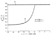
図2は、測定EDFAゲインを、EDFAに入力する1550nm入力信号パワーの関数として2本の曲線を示したものである。曲線50は、動的制御回路のスイッチがオンのときのEDFAゲインv入力パワー、曲線52は、ポンプレーザパワーがその最大値に固定されているときのEDFAゲインv入力パワーを示す。図2に示されるように、本発明の原理による動的ゲイン制御システムは、およそ−10dBmから−35dBmで変化する入力信号パワーにおいても、EDFAゲインを比較的一定に維持する。
【0019】
図3は、入力パワーをEDFAvポンプ源電流に対応プロットしたものである。曲線54は、動的制御回路のスイッチがオフでありポンプ源電流が最大に設定されているときの入力パワーvポンプ源電流、曲線56は、動的ゲイン制御回路が作動し、バイアス電流I0が40mAに設定されているときの入力パワーvポンプ源電流を示す。図3は、この波長における反転を固定したEDFAの動的レンジが、約25dB(−35〜−10dBm)であることを示している。この動的レンジは、最大出力パワーが高いポンプレーザ(本実施例のポンプレーザについては、出力パワーの最大は、約70mW)を用いることで拡張可能である。
【0020】
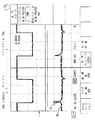
チャネルが追加あるいは減少された時、本実施例のEDFAにおける動的制御回路の動的挙動の一例を以下に示す。図4は、動的ゲイン制御システムの動的挙動検査を行うための測定セットアップを示す。1.55ミクロンファブリ−ペロレーザ60は、EDFA66の入力ポートにおいてレーザ60のパワーがPi=−11.5dBmとなる。1550.0nmでは、10Hz矩形波信号によるレーシングモードの変調はない。矩形波生成器62は、10Hzの矩形波信号を生成し、可変レーザ源64からの1550.0nm信号について、6チャネルのうち5チャネルの追加あるいは減少を誘導し、本実施例の反転を固定したEDFA66に、パワーPi=−17.5dBmの可変レーザ64が入力する。オシロスコープ68を使用して、総入力パワー(EDFA66に入力するファブリ−ペロレーザ60および可変レーザ64の合計値)およびEDFA66からの1550nmでの出力パワーを、時間の関数として測定する。1550nmでの出力パワーを測定するには、0.5nm帯域フィルタ70を1550nmに調整して使用する。
【0021】
図5は、オシロスコープ68のチャネル1上の総入力パワーのプロット74、および動的制御回路のスイッチがオフの時、オシロスコープ68のチャネル2上の1550nmにおけるEDFA66の出力パワープロット76を示す(両パワースケールは線形である)。この場合、他のチャネルが時間周期78の間減少されているとき、1550nm信号の出力パワーは、3dBを越えて上昇する。
【0022】
図6は本実施例の動的制御回路のスイッチがオンになっている時の結果を示す。この場合、1550nm出力80は、2ミリ秒の間元の値に戻り、エクスカーションピーク82は、約1.7dBまで減少する。このように、図5のプロットにより、動的制御回路が、チャネルの追加/減少の間に、本発明の原理によって、EDFA66(図4)からの1550nm出力パワー信号に関連するゲインを維持する方法が示された。動的制御回路の反応時間をマイクロ秒に改善することにより、エクスカーションピーク82によって示されるゲイン過渡の性能は改善される。
【0023】
このような動的ゲイン制御システムは、従来のシステムの短所を克服し、入力信号に独立であり、比較的一定したスペクトルゲインを有する光増幅器が得られる。上述の制御方法あるいはその変形を実行するにあたり、要素の省略または追加、あるいは異なる要素の使用により、動的ゲイン制御システムの他の構成も可能である。例えば、動的ゲイン制御システムからより高速で、なめらかな反応が得られるように、フィードバックエレクトロニクスを改善することも可能である。さらに、上述の実施例は、エルビウムドープファイバ増幅器の動的ゲイン制御を扱ったが、本発明の動的ゲイン制御システムは、他の光増幅器と共に使用することも可能であり、スペクトルゲインは、ポンプ光損失を測定し、ポンプ源の出力を制御するフィードバックシステムの入力信号としてそれを用いることで維持される。このように、光増幅器は、エルビウムドーププラナ波長増幅器、およびエルビウム−イッテルビウムドープ増幅器のような他の稀土類ドープ増幅器でも可能である。さらに、動的ゲイン制御システムは、入出力ポンプパワーを測定し、その測定値からポンプパワーロスを判定するように記述されたが、ポンプパワーの入出力測定は、実際の入出力ポンプパワーに関連するこれら値、あるいは他のパラメータの分数測定でも達成され、ポンプパワーロスの判定は、ポンプパワーロスに関するこれらあるいは他のパラメータ測定によっても達成される。
【0024】
さらに、動的ゲイン制御システムは、いくつかの単純な要素を含むように記述されたが、動的ゲイン制御システムとその構成要素は、特定用途向け集積回路、ソフトウェア駆動処理回路、または、それぞれの要素の他の配置によって構成されてもよい。以上は、本発明の原理の適用を図示的に記述したものにすぎず、当業者であれば分かるように、ここに図示および記述された例示的な適用に忠実に従うことなく、また、本発明の趣旨から逸脱することなく、本発明にこれらおよび他の変形、構成および方法を施すことが可能である。
【図面の簡単な説明】
【図1】本発明による、ポンプ光損失制御により反転/ゲインを固定する動的ゲイン制御システムの実施例におけるEDFAの概略図である。
【図2】動的ゲイン制御システムのスイッチオン/オフによる、1550nmにおける、信号入力パワー関数であるEDFAのゲインをプロットしたグラフである。
【図3】動的ゲイン制御システムのスイッチオン/オフによる、1550nmにおける、信号入力パワー関数であるポンプレーザ電流をプロットしたグラフである。
【図4】動的ゲイン制御システムの実施例における測定セットアップのブロック図である。
【図5】動的ゲイン制御システムのスイッチがオフの時、EDFAにおけるチャネル1での総入力パワー、及び1550nmでのチャネル2での出力パワーの測定を示す図である。
【図6】動的ゲイン制御システムのスイッチがオンの時、EDFAにおけるチャネル1での総入力パワー、及び1550nmでのチャネル2での出力パワーの測定を示す図である。
【符号の説明】
10 エルビウムドープファイバ増幅器(EDFA)
12 ポンプ源
14 単一波長低パーセンテージ反射器
16 光ファイバライン
20 光検出器
22 タップカプラ
24 エルビウムドープファイバ(EDF)
26 波長分割多重(WDM)
28 光検出器
30 処理回路
32 負フィードバックループ
34 基準電圧源
36,38 抵抗
40 動作増幅器
42 コンデンサ
44 可変ポンプレーザダイオード電流Iv=GU源
46 バイアス電流I0源
60 ファブリ−ペロレーザ
62 矩形波生成器
64 可変レーザ
66 エルビウムドープファイバ増幅器(EDFA)
68 オシロスコープ
70 帯域フィルタ[0001]
TECHNICAL FIELD OF THE INVENTION
The present invention relates to an optical communication system, and more particularly, to a dynamic gain control system for an optical amplifier.
[0002]
[Prior art]
An optical communication system is desirable because a wide band can be used for the information signal channel. Due to the speed limitations of optical transmitters and receivers, it is difficult to take full advantage of this broadband while using a single wavelength. Thus, high capacity optical transmission systems generally use all available bandwidth by combining high speed systems by wavelength division multiplexing (WDM) onto a single fiber. Such WDM optical transmission systems typically use rare earth-doped fiber optical amplifiers (eg, those doped with erbium or erbium-ytterbium) to compensate for fiber links and splitting losses. Optical amplifiers add undesirable noise to the system under certain conditions. In addition, rare earth doped fiber amplifiers remain a challenge in some applications.
[0003]
Gain transients in optical amplifiers are a major problem for wavelength division multiplexed (WDM) optical systems. In this system, channels are added or decreased due to network reconfiguration or failure. The addition of a channel weakens the power of the current channel and renders the receiver insensitive. Due to the reduced channel, the residual channel power exceeds the threshold of the non-linear effect, which causes residual reflections such as stimulated Brillouin scattering (SBS) causing unwanted reflections and noise and four-wave mixing (FWM) which adds crosstalk between channels. Channels are more prone to errors. Error bursts in the surviving or current channel resulting from these power transients are unacceptable to the service provider.
[0004]
Further, in erbium-doped fiber amplifiers, the gain is not uniform over the light wavelength. This is because the gain of the erbium-doped amplifier is uniquely determined by the absorption / divergence wavelength spectrum of erbium ions in the fiber. This is a significant problem for WDM systems where multiple wavelengths are amplified simultaneously. Therefore, there is a need for an erbium-doped fiber amplifier (EDFA) that has a relatively constant multi-channel gain and a small gain variation between WDM channels regardless of changes in the number, power, wavelength, and modulation method of WDM gravity channels. . Erbium-doped fiber (EDF) has an inversion level, which causes some variation in multi-channel gain. The inversion level refers to the number of inverted or excited erbium ions out of all erbium ions in the fiber. For an ideal version of the EDFA, the gain variation between WDM channels is zero. In fact, even with a low multi-channel gain variation of the EDFA, some (eg, 1 dB) channel gain variation still occurs between the channels, which is reduced by the use of passive optical filters, thereby making it relatively flat and constant. The multi-channel gain v and wavelength spectrum of the EDFA are obtained within the operating wavelength range of the EDFA.
[0005]
1996 Conference on Optical Amplifiers and Their Applications, A.A. of Postdeadline Paper PDP4, a technical digest of OAA '96. K. According to Srivastava et al., "First Gain Control of Erbium-Doped Fiber Amplifiers," an output power control system measures the output power from the channel and drives the pump laser with a feedback loop to relatively control the output power of the channel. Kept constant. However, this system does not provide true gain control. This is because the gain control can be obtained only when the input power is constant. The disadvantage of this solution is that if the channel itself used to measure the output power is reduced, it will not work. Further, as described above, the system cannot maintain multi-channel gain and non-variation in the multi-channel gain spectrum when the measured input power of the channel changes.
[0006]
In 1993, San Jose, California, Optical Fiber Telecommunications Conference (OFC'93) paper Tu15 (pp. 40-42), K.M. According to Motoshima et al., "Dynamic Compensation of Transient Gain Saturation by Pump Feedback Control in Erbium-Doped Fiber Amplifiers," the system has an extra probe signal whose wavelength lies in the gain wavelength region of the EDFA. However, it is not present at possible signal wavelengths, thereby measuring and stabilizing the gain. Then, both the input power and the output power of the probe signal are measured, and the actual gain is determined. By using a feedback circuit to supply the pump laser diode current and its power, the system produces a relatively constant gain. The disadvantage of this technique is that an extra DFB laser for supplying the probe signal and an acute wavelength multiplexer for adding and extracting the probe signal are required for all EDFAs, which reduces the manufacturing cost of the EDFA. To increase.
[0007]
The 1996 conference on optical amplifiers and their applications, J. of Paper FB2 (pages 77-80), a technical digest of OAA '96. According to Massicott et al., "Asymmetrically Controlled Laser Cavities Achieving Low-Noise Operation of All-Optical-Gain-Controlled Erbium-Doped Fiber Amplifiers," an optical gain clamping solution is reported. However, the use of optical gain clamps requires at least two extra signal wavelength optical reflectors. In addition, the available pump power increases the noise type and reduces the amplifier output power, as filters and / or reflectors for gain clamp control introduce additional losses in the signal wavelength.
[0008]
Therefore, there is a need for an EDFA that overcomes the shortcomings of these conventional systems, has a relatively constant and multi-channel gain, and is independent of changes in the number of WDM input channels, power, wavelength and modulation method.
[0009]
[Problems to be solved by the invention]
A dynamic gain control system according to the principles of the present invention determines pump light loss and maintains the pump light loss relatively constant with changes in input channel. Thereby, the dynamic gain control system can maintain the inversion level of the optical amplifier. A relatively constant inversion level, ie, results in a relatively constant gain for the channel (multi-channel gain) regardless of changes in the number of input channels, power, wavelength, and / or modulation method.
[0010]
To achieve the above and other aspects of the invention, a dynamic gain control system has a pump source that provides pump light. The dynamic gain control system measures a portion of the input pump light flowing to the optical amplifier and measures a portion of the pump light emitted from the optical amplifier. The dynamic gain control determines the loss of the pump light based on the measured values of the input pump light and the output pump light. Based on this pump light loss, the dynamic gain control system provides feedback to control the output pump light, regardless of the input channel and its associated power (eg, 50 dBm to 10 dBm input channel power). The pump light loss can be kept relatively constant (for example, 0.1 dB). As described above, the dynamic gain control system reduces the multi-channel gain change as a result of changing the input channel of the optical amplifier. According to some embodiments, the multi-channel wavelength gain spectrum may be complemented by using passive optical filter technology to reduce gain variation between channels over a wide input power range. .
[0011]
According to some embodiments of the present invention, the type of output power spectrum of the pump source is relatively constant (eg, ± 5%) even when the output power changes. The control of the output pump light is achieved, for example, by installing a 980 or 1480 nm pump source having a fixed bias current and temperature, and changing the output light of the pump source using an external modulator and attenuator. . Alternatively, the pump source is optically fixed at a single signal wavelength by using a single wavelength low percentage reflector (eg, a 4% fiber Bragg grating reflector at 978 nm) and the drive current of the pump source is reduced. The control changes the output power of the pump source. The dynamic control circuit is manufactured to solve the problem of gain transients, for example, to have a fast response time in the order of microseconds.
Other aspects and advantages of the present invention are described in detail below with reference to the drawings.
[0012]
BEST MODE FOR CARRYING OUT THE INVENTION
An embodiment of a dynamic gain control system according to the principles of the present invention will be described graphically below. The dynamic gain control system has a multi-channel gain by maintaining or fixing the average inversion of the EDF, and changes in the input channel, that is, the EDFA regardless of the number of WDM input channels, their power, wavelength and modulation method. Becomes possible. Further, a filter function is used to remove the fluctuation of the inter-channel gain of the EDFA. These features, and the dynamic characteristics of dynamic control using a fast negative feedback loop, solve the problem of gain transients.
[0013]
The gain λ, which is a function of wavelength, is a function of the length L of the erbium-doped fiber, the time of the erbium ions, and the position average inversion <N>. That is,
G (λ) L * [α (λ) + g * (λ)) <N> − (α (λ) + δ (λ))]
Here, α (λ) is an absorption rate, g * (λ) is a divergence rate, and δ (λ) is a background loss (all dB / m). The fixed inversion of erbium ions in the EDF results in a fixed multi-channel gain envelope and pump light loss. Thus, in this particular embodiment, the inversion level can be fixed by keeping the pump power loss Lp = P pump-in / P pump-out relatively constant for different WDM input channel powers. Here, P pump-in is the pump power input to the EDFA, and P pump-out is the pump power output from the EDFA.
[0014]
FIG. 1 is a schematic diagram of an
[0015]
Before coupling the input signal of the
[0016]
The
[0017]
The
[0018]
FIG. 2 shows two curves of the measured EDFA gain as a function of the 1550 nm input signal power input to the EDFA.
[0019]
FIG. 3 is a plot of input power versus EDFAv pump source current.
[0020]
An example of the dynamic behavior of the dynamic control circuit in the EDFA of this embodiment when a channel is added or reduced is shown below. FIG. 4 shows a measurement setup for performing dynamic behavior testing of a dynamic gain control system. For a 1.55 micron Fabry-
[0021]
FIG. 5 shows a
[0022]
FIG. 6 shows the result when the switch of the dynamic control circuit of this embodiment is turned on. In this case, the 1550
[0023]
Such a dynamic gain control system overcomes the disadvantages of conventional systems and results in an optical amplifier that is independent of the input signal and has a relatively constant spectral gain. Other configurations of the dynamic gain control system are possible, by omitting or adding elements, or using different elements in performing the above-described control methods or variations thereof. For example, it is possible to improve the feedback electronics so that a faster and smoother response is obtained from the dynamic gain control system. Further, while the above embodiments deal with dynamic gain control of an erbium-doped fiber amplifier, the dynamic gain control system of the present invention can also be used with other optical amplifiers, and the spectral gain can be reduced by pumping. It is maintained by measuring light loss and using it as an input signal to a feedback system that controls the output of the pump source. Thus, the optical amplifier can be other rare earth-doped amplifiers, such as an erbium-doped planar wavelength amplifier, and an erbium-ytterbium-doped amplifier. Further, while the dynamic gain control system has been described to measure the input and output pump power and determine the pump power loss from the measurement, the input and output measurement of the pump power is related to the actual input and output pump power. Fractional measurements of these values or other parameters are also achieved, and determination of pump power loss is also achieved by measuring these or other parameters related to pump power loss.
[0024]
Further, while the dynamic gain control system has been described as including several simple elements, the dynamic gain control system and its components may be implemented in an application specific integrated circuit, a software driven processing circuit, or a respective It may be constituted by another arrangement of the elements. The foregoing is only a graphical description of the application of the principles of the present invention, and as will be apparent to those skilled in the art, without faithfully following the exemplary application shown and described herein, and of the present invention. These and other modifications, configurations, and methods can be made to the present invention without departing from the spirit of the invention.
[Brief description of the drawings]
FIG. 1 is a schematic diagram of an EDFA in an embodiment of a dynamic gain control system for fixing inversion / gain by pump light loss control according to the present invention.
FIG. 2 is a graph plotting the gain of an EDFA as a function of the signal input power at 1550 nm with the dynamic gain control system switched on / off.
FIG. 3 is a graph plotting pump laser current as a function of signal input power at 1550 nm with the dynamic gain control system switched on / off.
FIG. 4 is a block diagram of a measurement setup in an embodiment of the dynamic gain control system.
FIG. 5 shows the measurement of the total input power on
FIG. 6 shows the measurement of the total input power on
[Explanation of symbols]
10 Erbium-doped fiber amplifier (EDFA)
12
26 Wavelength Division Multiplexing (WDM)
28 the
68
Claims (1)
該ポンプ源を固定されたバイアス電流と温度に固定し、そして外部変調器又は減衰器を用いて該ポンプ源の出力光を変化させることで、該パワースペクトルの安定化が行われることを特徴とする光増幅器の制御方法。A method for controlling an optical amplifier (24), comprising supplying pump light from a pump source (12), stabilizing a power spectrum of the pump light from the pump source (12), A method for controlling an optical amplifier that determines pump light loss and controls the pump light in relation to the pump light loss,
The power spectrum is stabilized by fixing the pump source at a fixed bias current and temperature, and changing the output light of the pump source using an external modulator or attenuator. Control method of the optical amplifier.
Applications Claiming Priority (2)
| Application Number | Priority Date | Filing Date | Title |
|---|---|---|---|
| US08/828,444 US5923462A (en) | 1997-03-28 | 1997-03-28 | Dynamic gain control system for optical amplifier and method thereof |
| US08/828444 | 1997-03-28 |
Publications (2)
| Publication Number | Publication Date |
|---|---|
| JPH10284788A JPH10284788A (en) | 1998-10-23 |
| JP3553361B2 true JP3553361B2 (en) | 2004-08-11 |
Family
ID=25251826
Family Applications (1)
| Application Number | Title | Priority Date | Filing Date |
|---|---|---|---|
| JP08059598A Expired - Fee Related JP3553361B2 (en) | 1997-03-28 | 1998-03-27 | Optical amplifier dynamic gain control system and method |
Country Status (5)
| Country | Link |
|---|---|
| US (1) | US5923462A (en) |
| EP (1) | EP0871302B1 (en) |
| JP (1) | JP3553361B2 (en) |
| CA (1) | CA2228227C (en) |
| DE (1) | DE69800149T2 (en) |
Families Citing this family (35)
| Publication number | Priority date | Publication date | Assignee | Title |
|---|---|---|---|---|
| GB2318471A (en) * | 1996-10-18 | 1998-04-22 | Stc Submarine Systems Ltd | Semiconductor laser amplifiers for transient suppression in optical wavelength division multiplex networks |
| DE19836373A1 (en) * | 1997-08-22 | 1999-03-11 | Samsung Electronics Co Ltd | Analog / digital double automatic power control device in optical fiber amplifier |
| JP3134854B2 (en) * | 1998-09-07 | 2001-02-13 | 日本電気株式会社 | Optical amplifier |
| US6163399A (en) * | 1998-12-08 | 2000-12-19 | Nortel Networks Limited | Method and apparatus for suppressing transients in optical amplifiers |
| JP4204693B2 (en) * | 1999-03-31 | 2009-01-07 | 三菱電機株式会社 | Optical amplifier |
| US6381560B1 (en) * | 1999-12-09 | 2002-04-30 | Lucent Technologies Inc. | Methods of modeling erbium doped fiber amplifiers |
| US6307670B1 (en) | 1999-12-14 | 2001-10-23 | Corning Incorporated | Pump power control for optical fiber amplifier |
| US6256138B1 (en) * | 2000-01-07 | 2001-07-03 | Lucent Technologies Inc | Fiber filter to improve return loss at signal band of a fiber amplifier for pump laser modules |
| FR2805092A1 (en) * | 2000-02-10 | 2001-08-17 | Corning Inc | LASER SOURCE THAT CAN BE SELECTED BY MEMS |
| WO2001080380A1 (en) * | 2000-04-13 | 2001-10-25 | Corning Incorporated | Method for controlling performance of optical amplifiers |
| US6631027B2 (en) * | 2000-04-13 | 2003-10-07 | Corning Incorporated | Universal controller for an optical amplifier that operates over a wide dynamic range of optical signals and optical amplifiers utilizing such controllers |
| US6366394B1 (en) | 2000-04-14 | 2002-04-02 | Institut National D'optique | Gain-locked dual stage optical amplifier |
| WO2001084679A1 (en) * | 2000-04-29 | 2001-11-08 | Corning Incorporated | Universal controller for an optical amplifier |
| US6490080B2 (en) | 2000-12-22 | 2002-12-03 | Ciena Corporation | Gain controlled optically pre-amplified receiver apparatus and method |
| US6424458B1 (en) | 2000-12-22 | 2002-07-23 | Ciena Corporation | Optical pre-amplifier apparatus and method for receiver performing windowed and gain change rate control |
| US6522461B1 (en) | 2000-12-22 | 2003-02-18 | Ciena Corporation | Optical pre-amplifier apparatus and method for receiver performing gain control according to LOS declaration |
| US6747774B2 (en) | 2001-07-19 | 2004-06-08 | Coadna Photonics, Inc. | Apparatus and method for controlling optical gain profiles |
| US6614572B2 (en) | 2001-07-19 | 2003-09-02 | Coadna Photonics, Inc. | Apparatus and method for controlling optical gain profiles in a temperature independent manner |
| US6989923B2 (en) * | 2001-08-08 | 2006-01-24 | Photuris, Inc. | Optical amplifier having automatic gain control with improved performance |
| US7061668B2 (en) * | 2002-03-21 | 2006-06-13 | Siemens Communications Inc. | Fast optical amplifier control circuit |
| US20040017603A1 (en) * | 2002-07-29 | 2004-01-29 | Paul Jay | Optical amplifier controller |
| US6738185B2 (en) | 2002-08-30 | 2004-05-18 | Sumitomo Electric Industries, Ltd. | Optical amplifier gain control method for optical amplifier and gain control circuit for optical amplifier |
| US6900934B2 (en) * | 2002-09-27 | 2005-05-31 | Avanex Corporation | Inversion level controller and system for optical amplifiers |
| US7877019B2 (en) * | 2002-10-16 | 2011-01-25 | Tyco Electronics Subsea Communications Llc | Optical receiver including a system and method of controlling gain of an optical amplifier |
| US7333732B2 (en) * | 2004-12-30 | 2008-02-19 | Tyco Telecommunications (Us) Inc. | Optical receiver |
| US7146110B2 (en) | 2003-02-11 | 2006-12-05 | Optium Corporation | Optical transmitter with SBS suppression |
| US7269347B1 (en) | 2003-05-28 | 2007-09-11 | Ciena Corporation | Optical receiver decision threshold tuning apparatus and method |
| US7483205B1 (en) * | 2003-05-29 | 2009-01-27 | Ciena Corporation | Transient optical power suppressing apparatus, method, and network |
| US6865017B2 (en) * | 2003-06-20 | 2005-03-08 | Oplink Communications, Inc. | Optical fiber amplifier with error correction |
| US7010189B2 (en) * | 2003-10-03 | 2006-03-07 | National Chiao Tung University | Optical monitoring apparatus for use in wavelength division multiplexing network |
| US7327958B2 (en) * | 2004-07-30 | 2008-02-05 | Lucent Technologies Inc. | Transient-based channel growth for optical transmission systems |
| US8373926B2 (en) * | 2004-12-10 | 2013-02-12 | Ciena Corporation | Differentiation of power and channel count changes in optically amplified links |
| JP4616668B2 (en) * | 2005-03-03 | 2011-01-19 | 日本電信電話株式会社 | Hybrid optical amplifier |
| JP4580404B2 (en) * | 2007-03-29 | 2010-11-10 | 富士通株式会社 | Optical amplifier |
| US9069060B1 (en) | 2013-03-13 | 2015-06-30 | Google Inc. | Circuit architecture for optical receiver with increased dynamic range |
Family Cites Families (7)
| Publication number | Priority date | Publication date | Assignee | Title |
|---|---|---|---|---|
| JPH02273976A (en) * | 1989-04-17 | 1990-11-08 | Nippon Telegr & Teleph Corp <Ntt> | Optical amplifier |
| JPH02308581A (en) * | 1989-05-24 | 1990-12-21 | Furukawa Electric Co Ltd:The | Light amplification |
| US5268786A (en) * | 1991-03-15 | 1993-12-07 | Mitsubishi Denki Kabushiki Kaisha | Optical fiber amplifier and its amplification method |
| US5374973A (en) * | 1993-09-21 | 1994-12-20 | Alcatel Network Systems, Inc. | Optical amplifier |
| US5563732A (en) * | 1994-01-06 | 1996-10-08 | At&T Corp. | Laser pumping of erbium amplifier |
| US5541766A (en) * | 1994-11-30 | 1996-07-30 | At&T Corp. | Gain control for optically amplified systems |
| JPH08304856A (en) * | 1995-05-01 | 1996-11-22 | Ando Electric Co Ltd | Optical fiber amplifier |
-
1997
- 1997-03-28 US US08/828,444 patent/US5923462A/en not_active Expired - Lifetime
-
1998
- 1998-01-27 CA CA002228227A patent/CA2228227C/en not_active Expired - Fee Related
- 1998-03-17 DE DE69800149T patent/DE69800149T2/en not_active Expired - Lifetime
- 1998-03-17 EP EP98301970A patent/EP0871302B1/en not_active Expired - Lifetime
- 1998-03-27 JP JP08059598A patent/JP3553361B2/en not_active Expired - Fee Related
Also Published As
| Publication number | Publication date |
|---|---|
| EP0871302B1 (en) | 2000-05-17 |
| DE69800149D1 (en) | 2000-06-21 |
| EP0871302A3 (en) | 1998-11-25 |
| JPH10284788A (en) | 1998-10-23 |
| CA2228227C (en) | 2002-03-26 |
| CA2228227A1 (en) | 1998-09-28 |
| US5923462A (en) | 1999-07-13 |
| EP0871302A2 (en) | 1998-10-14 |
| DE69800149T2 (en) | 2000-11-09 |
Similar Documents
| Publication | Publication Date | Title |
|---|---|---|
| JP3553361B2 (en) | Optical amplifier dynamic gain control system and method | |
| EP0897205B1 (en) | Method and device for optical amplification and system comprising the device | |
| US6342965B1 (en) | Optical fiber amplifier and dispersion compensating fiber module for optical fiber amplifier | |
| US20070230968A1 (en) | Optical transmission apparatus | |
| US6259556B1 (en) | Optical fibre amplifier having a controlled gain | |
| CA2341726A1 (en) | Gain control and shaping of edfas via dual cavity gain control | |
| JP2002208758A (en) | Optical amplifier device | |
| KR100582542B1 (en) | Long-wavelength-band gain-controlled optical amplifier | |
| KR100687751B1 (en) | Erbium doped fiber amplifier and method for amplifing to reduce the transient behavior of osnr and ber in dynamic wdm system | |
| US6198570B1 (en) | Optical filter, manufacturing method thereof, and optical amplifier equipped with said optical filter | |
| EP1528698B1 (en) | Raman amplifier with gain control | |
| Pratt et al. | Gain control in L-band EDFAs by monitoring backward traveling C-band ASE | |
| Van der Plaats et al. | Dynamic pump-loss controlled gain-locking system for erbium-doped fiber amplifiers in multi-wavelength networks | |
| EP1237238A2 (en) | Gain-clamped optical fibre amplifier | |
| JPH05343788A (en) | Optical fiber amplifier and optical signal transmission system | |
| JP3250473B2 (en) | Optical amplifier | |
| Krol et al. | Gain variations in optically gain clamped erbium doped fiber amplifiers | |
| KR20030086808A (en) | Optical fiber amplification method and apparatus for controlling gain | |
| JP2001136127A (en) | Optical amplifier | |
| Kim et al. | Wideband multiwavelength erbium-doped fiber ring laser | |
| KR0183913B1 (en) | Erbium doped fiber amplifier having flat gain and low noise-figure | |
| KR0183911B1 (en) | Optical fiber amplifier having flat gain and low noise-figure | |
| Altay et al. | Saturation characteristics of a gain-clamped extended length L-band erbium doped fiber amplifier | |
| KR100194960B1 (en) | Optical amplifier | |
| KR100564745B1 (en) | Optical amplifier and gain control method using optical delay |
Legal Events
| Date | Code | Title | Description |
|---|---|---|---|
| A521 | Written amendment |
Free format text: JAPANESE INTERMEDIATE CODE: A523 Effective date: 20040308 |
|
| A61 | First payment of annual fees (during grant procedure) |
Free format text: JAPANESE INTERMEDIATE CODE: A61 Effective date: 20040428 |
|
| R150 | Certificate of patent or registration of utility model |
Free format text: JAPANESE INTERMEDIATE CODE: R150 |
|
| R250 | Receipt of annual fees |
Free format text: JAPANESE INTERMEDIATE CODE: R250 |
|
| FPAY | Renewal fee payment (event date is renewal date of database) |
Free format text: PAYMENT UNTIL: 20080514 Year of fee payment: 4 |
|
| FPAY | Renewal fee payment (event date is renewal date of database) |
Free format text: PAYMENT UNTIL: 20080514 Year of fee payment: 4 |
|
| FPAY | Renewal fee payment (event date is renewal date of database) |
Free format text: PAYMENT UNTIL: 20080514 Year of fee payment: 4 |
|
| FPAY | Renewal fee payment (event date is renewal date of database) |
Free format text: PAYMENT UNTIL: 20090514 Year of fee payment: 5 |
|
| FPAY | Renewal fee payment (event date is renewal date of database) |
Free format text: PAYMENT UNTIL: 20090514 Year of fee payment: 5 |
|
| FPAY | Renewal fee payment (event date is renewal date of database) |
Free format text: PAYMENT UNTIL: 20100514 Year of fee payment: 6 |
|
| FPAY | Renewal fee payment (event date is renewal date of database) |
Free format text: PAYMENT UNTIL: 20110514 Year of fee payment: 7 |
|
| FPAY | Renewal fee payment (event date is renewal date of database) |
Free format text: PAYMENT UNTIL: 20120514 Year of fee payment: 8 |
|
| FPAY | Renewal fee payment (event date is renewal date of database) |
Free format text: PAYMENT UNTIL: 20130514 Year of fee payment: 9 |
|
| R250 | Receipt of annual fees |
Free format text: JAPANESE INTERMEDIATE CODE: R250 |
|
| R250 | Receipt of annual fees |
Free format text: JAPANESE INTERMEDIATE CODE: R250 |
|
| R250 | Receipt of annual fees |
Free format text: JAPANESE INTERMEDIATE CODE: R250 |
|
| LAPS | Cancellation because of no payment of annual fees |