JP3553281B2 - Lens parts - Google Patents
Lens parts Download PDFInfo
- Publication number
- JP3553281B2 JP3553281B2 JP20784696A JP20784696A JP3553281B2 JP 3553281 B2 JP3553281 B2 JP 3553281B2 JP 20784696 A JP20784696 A JP 20784696A JP 20784696 A JP20784696 A JP 20784696A JP 3553281 B2 JP3553281 B2 JP 3553281B2
- Authority
- JP
- Japan
- Prior art keywords
- hole
- lens
- package
- optical semiconductor
- metal cap
- Prior art date
- Legal status (The legal status is an assumption and is not a legal conclusion. Google has not performed a legal analysis and makes no representation as to the accuracy of the status listed.)
- Expired - Fee Related
Links
Images


Description
【0001】
【発明の属する技術分野】
本発明は、光半導体のパッケージに使用される気密構造のレンズ部品に関するものである。
【0002】
【従来の技術】
従来、光半導体モジュールは、円筒型の容器内に発光素子または受光素子のみが収納されていたが、近年、特に光通信用の光半導体モジュールでは取り扱う光ビームに高い品位が要求されるようになり、その形態が制御機能等を取り込むことが可能な箱型のものが多くなっている。図3は、光半導体モジュールの一例の断面図である。この光半導体モジュールは、光半導体として半導体レーザー10とコリメータレンズ6を光半導体用パッケージ4(以下パッケージ4と称す)内に備えている。半導体レーザー10は、サブキャリア11、ベース12を介してスペーサ13に固定してあり、このスペーサ13をパッケージ4の底部4dに固定してある。ベース12にはレンズ系としてコリメータレンズ6を設けてある。このコリメータレンズ6は、レンズホルダ6aに固定してあり、このレンズホルダ6aを位置および角度調整して半導体レーザー10の出射光が平行ビームになるようにした後、ベース12にYAG溶接などを用いて固定している。
【0003】
コリメータレンズ6から出射された光ビームは、パッケージ4の側面にある孔部4aを通して外部に導かれる。この光ビームは金属製のスリーブ7に挿入されたレンズ2により集光され、フェルール8に固定された光ファイバ9に入射される。このフェルール8は、スリーブ7に挿入されYAG溶接などを用いて固定されている。
【0004】
前記スリーブ7は、その貫通孔7aに接着剤3で固着されたレンズ2を備えている。このスリーブ7は、半田に対して濡れ性のよい金属製のパッケージ4の孔部4aに嵌入され、その外面を半田5を使用して気密固着されている。
【0005】
【発明が解決しようとする課題】
しかしながら、前記スリーブ7の取付位置には、その外周とその貫通孔7aとの偏心精度、レンズ2の取付精度、パッケージ4の孔部4aの加工精度、スリーブ7の取付精度などの多くの累積する位置ずれ要素が存在し、そのどれか一つの要素が所定の精度から外れると半導体レーザー10から出射される光ビームの光軸20からレンズ2以降の光学系の光軸が外れて光半導体モジュールの出力が規格から外れて不良品となる問題があり、一方各部品の加工精度および取付精度を厳しくするとコストが高くなる問題がある。
【0006】
また、パッケージ4に半導体レーザー10等を組みつけた後、蓋4fで気密構造にできない場合には、光半導体モジュールの組み立て工程は、最後の光ファイバ9の組みつけまでを一貫して行うか、またはパッケージ4の孔部4aの内側開口面に透明な窓部材4eを設けねばならず、製造工程の自由度に問題がある。
【0007】
本発明は、以上のような従来の光半導体モジュールの製造上の問題点を解決し、効率の良い光半導体モジュールの製造を可能にするレンズ部品を提供することを目的とする。
【0008】
【課題を解決するための手段】
本願発明に係るレンズ部品は、頂頭部に貫通孔を有し、その頂頭部から延在して一様な外径の円筒状中空部を有し、その円筒状中空部の開口端に鍔部を有する金属製キャップと、その金属製キャップの頂頭部の貫通孔に気密固着されたレンズとからなる光半導体用パッケージの孔部に嵌入固着されるレンズ部品において、前記金属製キャップの円筒状中空部の外径が嵌入される光半導体用パッケージの孔部の内径に対して接合位置調整用の間隙を設けた値に決められており、且つ金属製キャップの鍔部の面に光半導体用パッケージの孔部の開口端面に固着するための気密溶接用の微小突起輪が形成してあることを特徴とする。
【0009】
本発明のレンズ部品によれば、金属製キャップの円筒状中空部の外径が嵌入される光半導体用パッケージの孔部の内径に対して接合位置調整用の間隙を設けた値に決められており、且つ金属製キャップの鍔部の面に光半導体用パッケージの孔部の開口端面に固着するための気密溶接用の微小突起輪が形成してあるので、レンズ部品の金属製キャップの円筒状中空部を光半導体用パッケージの孔部に嵌入してレンズ部品を光半導体の光軸と直交する方向の所定範囲内の位置に調整した後、その鍔部の面に形成された微小突起輪を光半導体用パッケージの孔部の開口端面に当接させ光半導体用パッケージとレンズ部品との間に所定の電流を流すだけで微小突起輪を溶かして所定の取付位置に気密固着できる。
【0010】
【発明の実施の形態】
本発明のレンズ部品は、その金属製キャップの頂頭部に貫通孔を有し、その貫通孔にレンズが気密固着されており、その頂頭部から延在して一様な外径の円筒状中空部を有しており、その一様な外径は光半導体用パッケージ(以下再びパッケージと称す)の孔部の内径より小さく、孔部の内径との間隙を接合位置調整用として使用できる。その円筒状中空部の開口端に設けられた鍔部の面には、パッケージの孔部の開口端面に固着するための気密溶接用の微小突起輪が形成してあり、パッケージの孔部に嵌入されパッケージに収納される光半導体の光軸と直交する方向の位置が調整された後、微小突起輪がパッケージの孔部の開口端面に当接され通電されて所定の取付位置に気密固着されるものである。
【0011】
金属製キャップとしては、通電により溶接可能な金属材料であればステンレス等の材料も使用可能であり、特に、レンズに使用される光学ガラス材料と膨張係数が近く、金属製の薄板からプレス成形などにより安価に大量生産可能な鉄−ニッケル合金、鉄−ニッケル−コバルト合金(所謂コバール合金)などの材料が好ましい。金属製キャップの頂頭部の貫通孔としては、気密固着されるレンズよりも僅かに大きい口径のもの、レンズよりも僅かに小さい口径のもの、円筒状中空部の内径とほぼ同じ口径のものなどがある。この金属製キャップの頂頭部から延在して一様な外径の円筒状中空部は、その長さがレンズの焦点距離、パッケージへのレンズ部品の取付形態などに従って決められ、その外径が嵌入される光半導体用パッケージの孔部の内径に対して接合位置調整用の間隙を設けた値に決められる。円筒状中空部の開口端の鍔部は、パッケージの孔部よりも大きい直径を有しており、そのパッケージ側の面には、パッケージの孔部の開口端面に固着するため溶接の際に切れ目の生じない気密溶接用の微小突起輪が形成してあり、その断面形状は、開口端面に当接する部分が尖った三角形や楔形などの形状をしていて、通電によりその先端に電流が集中して当接部が溶け易いものであることが好ましい。
【0012】
レンズとしては、BK−7、TaF−3などの光学ガラスを球形に加工した球レンズ、球レンズを研削して金属製キャップとの接合部を円筒状に加工したドラム状レンズなどが使用可能であり、そのレンズは金属製キャップの貫通孔に低融点ガラスなどを用いた接着剤を使用して加熱処理されて気密固着される。このレンズの表面には目的に応じて反射防止膜、フィルタ等を設けてもよい。
【0013】
光半導体用パッケージとしては、溶接に適した金属製の場合には、その所定の位置に孔部と平滑な開口端面を設けるだけでよいが、それ以外の場合、光半導体用パッケージの孔部の開口端面には、溶接に適した金属製のリング状部材をインサート射出成形や蝋着けなどにより取付けておき、リングの表面に当接したレンズ部品の微小突起輪を通電して溶かした際、レンズ部品を気密固着可能なものにしておく。
【0014】
【実施例】
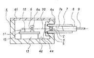
図1及び図2は、本発明に係るレンズ部品の説明図であって、1は金属製キャップを示しており、前記で説明した図3と同一部分には同一符号を付してそれぞれ示している。
【0015】
本発明のレンズ部品は、図1に示すように、コバール合金製の金属製キャップ1の頂頭部1aの中央に直径が1.6mmの貫通孔1bが明けられており、その頂頭部1aから延在してレンズ2の光軸方向の固定位置に応じた長さ4.0mmの一様な外径3.6mmの円筒状中空部1cを有し、その円筒状中空部1cの開口端1dに直径8mmで厚さ1.0mmの鍔部1eを有している。この鍔部1eのパッケージの孔部の開口端面に当接する側の面に気密溶接用の高さ0.1mmの断面形状が楔形をした微小突起輪1fを形成してある。この金属製キャップ1の頂頭部1aの貫通孔1bには光学ガラス材料のBK−7からなる直径1.5mmの球レンズ2が、低融点ガラスを主成分とする接着剤3により気密固着されている。
【0016】
上記のレンズ部品をパッケージ4に気密溶接固着して光半導体モジュールを組み立てる場合を説明する。図2に示すように、レンズ部品の金属製キャップ1の円筒状中空部1cの外径は3.6mmで、嵌入されているパッケージ4の孔部4aの内径4.0mmより接合位置調整用の間隙4cの0.4mmだけ小さくしてあり、この間隙4cを利用して半導体レーザー10の光軸20と直交する方向に対してレンズ部品の取付位置が調整される。この調整の後、図1に示された金属製キャップ1の鍔部1eの面に形成された気密溶接用の微小突起1fがパッケージ4の孔部4aの開口端面4bに当接され通電されて溶けて固着して溶接輪1gとなる。この通電によりレンズ部品の光軸20方向の位置が所定の規格範囲内にはいり、最終的にレンズ部品は所定の取付位置に溶接され気密固着されている。このレンズ2が取り付けられたパッケージ4に半導体レーザー10等を組みつけて蓋4fで密閉して気密構造とした後、半導体レーザー10から出射される光ビームを光パワーメータを使用してモニターしながらフェルール8および光ファイバ9を備えたスリーブ7を光出力が最大になる位置に調整して、その位置にYAG溶接などを用いて固定される。
【0017】
上記のレンズ部品をパッケージ4に固着する場合を説明する。先ず、パッケージ4を、その孔部4aにレンズ部品が嵌入できる向きで溶接装置のステージの所定の位置に精確に固定し、金属製の開口端面4bにパッケージ4側のプラス電極を取付る。次いで、レンズ部品を、後に取付られる半導体レーザー10の光軸20の方向及び光軸20と直交する方向に移動調整可能な移動テーブルに備えられ中央に観察孔が設けられたマイナス電極が接続された取付部に、そのレンズ2が突き出す方向に向けて鍔部1eの開口端1d側の面を当接させて取付る。移動テーブルを操作してレンズ部品の円筒状中空部1cを孔部4aに嵌入し、0.4mmの接合位置調整用の間隙4cを利用して光半導体の光軸と直交する方向の位置を調整する。この位置調整は、レンズの中心位置を簡単な光ファイバ光学系を使用してモニターしながら行う。光軸20と直交する方向の位置調整が終われば、移動テーブルを光軸20方向のパッケージ4側に動かしてレンズ部品の微小突起輪1fを開口端面4bに当接させ鍛圧を加えて微小突起輪1をパッケージ4の開口端面4bに突き刺し、所定の条件でプラス電極とマイナス電極間に通電すると気密溶接されて固着が完了し、図2に示すような取付状態となる。
【0018】
【発明の効果】
本発明のレンズ部品によれば、気密構造にすることが可能なレンズ付きの光半導体用パッケージが効率良く製造できるので、光半導体モジュールの製造工程の自由度が広がり、且つ部品コストの低減が可能となる実用上優れた効果を奏するものである。
【図面の簡単な説明】
【図1】本発明のレンズ部品の説明図
【図2】本発明のレンズ部品が装着された光半導体モジュールの説明図
【図3】従来の光半導体モジュールの説明図
【符号の説明】
1 金属製キャップ
1a 頂頭部
1b 貫通孔
1c 円筒状中空部
1d 開口端
1e 鍔部
1f 微小突起輪
1g 溶接輪
2 レンズ
3 接着剤
4 光半導体用パッケージ
4a 孔部
4b 開口端面
4c 接合位置調整用の間隙
4d 底部
4e 窓部材
4f 蓋
20 光軸[0001]
TECHNICAL FIELD OF THE INVENTION
The present invention relates to an airtight lens component used for an optical semiconductor package.
[0002]
[Prior art]
Conventionally, optical semiconductor modules contain only a light-emitting element or a light-receiving element in a cylindrical container. In recent years, especially in optical semiconductor modules for optical communication, high-quality light beams are required. In many cases, the form of the box type can take in a control function or the like. FIG. 3 is a sectional view of an example of the optical semiconductor module. This optical semiconductor module includes a
[0003]
The light beam emitted from the
[0004]
The
[0005]
[Problems to be solved by the invention]
However, in the mounting position of the
[0006]
In addition, after the
[0007]
SUMMARY OF THE INVENTION An object of the present invention is to solve the above-described problems in the production of the conventional optical semiconductor module and to provide a lens component that enables efficient production of the optical semiconductor module.
[0008]
[Means for Solving the Problems]
The lens component according to the present invention has a through hole at the top, a cylindrical hollow portion extending from the top and having a uniform outer diameter, and a flange at the open end of the cylindrical hollow portion. A lens cap fitted and fixed in a hole of an optical semiconductor package including a metal cap having a metal cap and a lens hermetically sealed in a through hole at the top of the metal cap. The outer diameter of the portion is determined to be a value provided with a gap for adjusting the joining position with respect to the inner diameter of the hole of the optical semiconductor package into which the optical semiconductor package is inserted, and the optical semiconductor package is provided on the surface of the flange portion of the metal cap. A small projection ring for hermetic welding for fixing to the opening end face of the hole.
[0009]
According to the lens component of the present invention, the outer diameter of the cylindrical hollow portion of the metal cap is determined to be a value provided with a gap for adjusting the joining position with respect to the inner diameter of the hole of the optical semiconductor package to be fitted. In addition, since a small projection ring for airtight welding for fixing to the opening end surface of the hole of the optical semiconductor package is formed on the surface of the flange portion of the metal cap, the cylindrical shape of the metal cap of the lens component is formed. After the hollow part is fitted into the hole of the optical semiconductor package and the lens component is adjusted to a position within a predetermined range in a direction orthogonal to the optical axis of the optical semiconductor, the minute projection ring formed on the surface of the flange is removed. The minute protrusion ring can be melted and hermetically fixed to a predetermined mounting position only by bringing the optical semiconductor package into contact with the opening end surface of the hole of the optical semiconductor package and flowing a predetermined current between the optical semiconductor package and the lens component.
[0010]
BEST MODE FOR CARRYING OUT THE INVENTION
The lens component of the present invention has a through hole at the top of the metal cap, the lens is hermetically fixed to the through hole, and a cylindrical hollow having a uniform outer diameter extending from the top. The uniform outer diameter is smaller than the inner diameter of the hole of the optical semiconductor package (hereinafter, referred to as a package again), and the gap with the inner diameter of the hole can be used for adjusting the joining position. On the surface of the flange provided at the opening end of the cylindrical hollow portion, a minute projection ring for airtight welding for fixing to the opening end surface of the hole of the package is formed, and fitted into the hole of the package. After the position of the optical semiconductor housed in the package in the direction orthogonal to the optical axis is adjusted, the minute projection ring is brought into contact with the opening end face of the hole of the package and is energized to be hermetically fixed at a predetermined mounting position. Things.
[0011]
As the metal cap, a material such as stainless steel can be used as long as it is a metal material that can be welded by energization.In particular, the expansion coefficient is close to that of the optical glass material used for the lens. Materials such as iron-nickel alloys and iron-nickel-cobalt alloys (so-called Kovar alloys) that can be mass-produced at low cost are preferable. As the through-hole at the top of the metal cap, one having a slightly larger diameter than the lens to be hermetically fixed, one having a slightly smaller diameter than the lens, one having a diameter substantially the same as the inner diameter of the cylindrical hollow portion, etc. is there. The length of the cylindrical hollow portion extending from the top of the metal cap and having a uniform outer diameter is determined according to the focal length of the lens, the mounting form of the lens component to the package, and the like. The value is determined by providing a gap for adjusting the bonding position with respect to the inner diameter of the hole of the optical semiconductor package to be inserted. The flange at the open end of the cylindrical hollow portion has a diameter larger than that of the hole of the package, and the surface on the package side has a cut at the time of welding to be fixed to the open end of the hole of the package. A small projection ring for airtight welding that does not cause air leakage is formed, and its cross-sectional shape is a triangular shape or a wedge shape with a point that touches the opening end surface, and current concentrates at the tip by energization. It is preferable that the contact portion be easily melted.
[0012]
As the lens, a spherical lens obtained by processing optical glass such as BK-7 or TaF-3 into a spherical shape, or a drum-shaped lens obtained by grinding a spherical lens and processing a joint with a metal cap into a cylindrical shape can be used. The lens is heat-treated in a through hole of a metal cap using an adhesive made of low-melting glass or the like, and is air-tightly fixed. An antireflection film, a filter, or the like may be provided on the surface of the lens according to the purpose.
[0013]
When the optical semiconductor package is made of metal suitable for welding, it is sufficient to provide a hole and a smooth opening end face at a predetermined position, but otherwise, the hole of the optical semiconductor package is not required. A metal ring-shaped member suitable for welding is attached to the opening end face by insert injection molding or brazing, etc., and when the minute projection ring of the lens part abutting the ring surface is energized and melted, Parts should be airtight.
[0014]
【Example】
1 and 2 are explanatory views of a lens component according to the present invention, in which 1 indicates a metal cap, and the same parts as those in FIG. I have.
[0015]
In the lens component of the present invention, as shown in FIG. 1, a through hole 1b having a diameter of 1.6 mm is formed in the center of a top 1a of a
[0016]
A case where the above-mentioned lens component is hermetically welded and fixed to the
[0017]
A case where the above lens component is fixed to the
[0018]
【The invention's effect】
ADVANTAGE OF THE INVENTION According to the lens component of this invention, since the optical-semiconductor package with a lens which can be made into an airtight structure can be manufactured efficiently, the degree of freedom of the manufacturing process of an optical-semiconductor module is expanded and the component cost can be reduced. This has a practically excellent effect.
[Brief description of the drawings]
FIG. 1 is an explanatory view of a lens component of the present invention. FIG. 2 is an explanatory view of an optical semiconductor module on which the lens component of the present invention is mounted. FIG. 3 is an explanatory view of a conventional optical semiconductor module.
DESCRIPTION OF
Claims (1)
前記金属製キャップの円筒状中空部の外径が嵌入される光半導体用パッケージの孔部の内径に対して接合位置調整用の間隙を設けた値に決められており、且つ金属製キャップの鍔部の面に光半導体用パッケージの孔部の開口端面に固着するための気密溶接用の微小突起輪が形成してあることを特徴とするレンズ部品。A metal cap having a through hole at the top, having a cylindrical hollow portion having a uniform outer diameter extending from the top, and having a flange at the open end of the cylindrical hollow portion, A lens part fitted and fixed in a hole of an optical semiconductor package comprising a lens hermetically fixed to a through hole at the top of a metal cap,
The outer diameter of the cylindrical hollow portion of the metal cap is determined to be a value provided with a gap for adjusting the joining position with respect to the inner diameter of the hole of the optical semiconductor package to be fitted therein , and the flange of the metal cap is provided. A lens part characterized in that a minute projection ring for hermetic welding is formed on a surface of the portion for fixing to an opening end surface of a hole of an optical semiconductor package.
Priority Applications (1)
| Application Number | Priority Date | Filing Date | Title |
|---|---|---|---|
| JP20784696A JP3553281B2 (en) | 1996-07-17 | 1996-07-17 | Lens parts |
Applications Claiming Priority (1)
| Application Number | Priority Date | Filing Date | Title |
|---|---|---|---|
| JP20784696A JP3553281B2 (en) | 1996-07-17 | 1996-07-17 | Lens parts |
Publications (2)
| Publication Number | Publication Date |
|---|---|
| JPH1031143A JPH1031143A (en) | 1998-02-03 |
| JP3553281B2 true JP3553281B2 (en) | 2004-08-11 |
Family
ID=16546503
Family Applications (1)
| Application Number | Title | Priority Date | Filing Date |
|---|---|---|---|
| JP20784696A Expired - Fee Related JP3553281B2 (en) | 1996-07-17 | 1996-07-17 | Lens parts |
Country Status (1)
| Country | Link |
|---|---|
| JP (1) | JP3553281B2 (en) |
Families Citing this family (3)
| Publication number | Priority date | Publication date | Assignee | Title |
|---|---|---|---|---|
| JP2006126272A (en) * | 2004-10-26 | 2006-05-18 | Nippon Electric Glass Co Ltd | Optical cap component |
| JP2006133504A (en) * | 2004-11-05 | 2006-05-25 | Nippon Electric Glass Co Ltd | Optical cap component |
| JP6902203B2 (en) | 2017-03-10 | 2021-07-14 | 日本電気硝子株式会社 | Optical cap parts |
-
1996
- 1996-07-17 JP JP20784696A patent/JP3553281B2/en not_active Expired - Fee Related
Also Published As
| Publication number | Publication date |
|---|---|
| JPH1031143A (en) | 1998-02-03 |
Similar Documents
| Publication | Publication Date | Title |
|---|---|---|
| KR920010947B1 (en) | Semiconductor light emitting device its component and lens position adjusting method | |
| US5033052A (en) | Optical semiconductor device and production method thereof | |
| JP3553281B2 (en) | Lens parts | |
| JPH0361927B2 (en) | ||
| JPH0713047A (en) | Optical element module | |
| US11515221B2 (en) | Housing for an optoelectronic device, and method for producing same, and lid for a housing | |
| JPH07168065A (en) | Optical semiconductor module | |
| JPH0933768A (en) | Optical semiconductor device | |
| JPH1031145A (en) | Method for attaching lens parts | |
| JP2022126893A (en) | Optical module and manufacturing method of the same | |
| JP2586123B2 (en) | Semiconductor laser module | |
| JP2940497B2 (en) | Optical semiconductor module | |
| JP2975813B2 (en) | Optical element module and method of assembling the same | |
| JP2516171Y2 (en) | Optical semiconductor element collimator | |
| JPH0747870Y2 (en) | Airtight container with optical window | |
| JPH02297988A (en) | Optical coupling system using optical semiconductor device | |
| JPH0529170U (en) | Laser diode module | |
| JPH0247609A (en) | Optical semiconductor assembly | |
| JP2003207693A (en) | Photosemiconductor module | |
| JP2959072B2 (en) | Light emitting module manufacturing method | |
| JPH08110447A (en) | Optical semiconductor module and its assembling method | |
| JPH02308209A (en) | Semiconductor light emitting device, its component and lens position adjusting method | |
| JPH0368906A (en) | Spherical lens parts | |
| JPH0348209A (en) | Semiconductor laser module for single-mode | |
| JP2581207B2 (en) | Airtight structure of optical fiber introduction section |
Legal Events
| Date | Code | Title | Description |
|---|---|---|---|
| A977 | Report on retrieval |
Free format text: JAPANESE INTERMEDIATE CODE: A971007 Effective date: 20031218 |
|
| A131 | Notification of reasons for refusal |
Free format text: JAPANESE INTERMEDIATE CODE: A131 Effective date: 20031224 |
|
| A521 | Written amendment |
Free format text: JAPANESE INTERMEDIATE CODE: A523 Effective date: 20040220 |
|
| TRDD | Decision of grant or rejection written | ||
| A01 | Written decision to grant a patent or to grant a registration (utility model) |
Free format text: JAPANESE INTERMEDIATE CODE: A01 Effective date: 20040415 |
|
| A61 | First payment of annual fees (during grant procedure) |
Free format text: JAPANESE INTERMEDIATE CODE: A61 Effective date: 20040428 |
|
| R150 | Certificate of patent or registration of utility model |
Free format text: JAPANESE INTERMEDIATE CODE: R150 |
|
| FPAY | Renewal fee payment (event date is renewal date of database) |
Free format text: PAYMENT UNTIL: 20090514 Year of fee payment: 5 |
|
| LAPS | Cancellation because of no payment of annual fees |