JP3553078B2 - Protection switch for battery operated devices - Google Patents
Protection switch for battery operated devices Download PDFInfo
- Publication number
- JP3553078B2 JP3553078B2 JP51459496A JP51459496A JP3553078B2 JP 3553078 B2 JP3553078 B2 JP 3553078B2 JP 51459496 A JP51459496 A JP 51459496A JP 51459496 A JP51459496 A JP 51459496A JP 3553078 B2 JP3553078 B2 JP 3553078B2
- Authority
- JP
- Japan
- Prior art keywords
- voltage
- cell
- contact
- electrically connected
- rechargeable battery
- Prior art date
- Legal status (The legal status is an assumption and is not a legal conclusion. Google has not performed a legal analysis and makes no representation as to the accuracy of the status listed.)
- Expired - Fee Related
Links
- 239000003990 capacitor Substances 0.000 claims description 2
- 230000003213 activating effect Effects 0.000 claims 2
- WHXSMMKQMYFTQS-UHFFFAOYSA-N Lithium Chemical compound [Li] WHXSMMKQMYFTQS-UHFFFAOYSA-N 0.000 claims 1
- 229910052744 lithium Inorganic materials 0.000 claims 1
- 229910001416 lithium ion Inorganic materials 0.000 description 16
- HBBGRARXTFLTSG-UHFFFAOYSA-N Lithium ion Chemical compound [Li+] HBBGRARXTFLTSG-UHFFFAOYSA-N 0.000 description 14
- PXHVJJICTQNCMI-UHFFFAOYSA-N nickel Substances [Ni] PXHVJJICTQNCMI-UHFFFAOYSA-N 0.000 description 9
- 229910052759 nickel Inorganic materials 0.000 description 5
- 230000008901 benefit Effects 0.000 description 4
- 238000010586 diagram Methods 0.000 description 4
- 230000001105 regulatory effect Effects 0.000 description 3
- 230000001413 cellular effect Effects 0.000 description 2
- 238000004519 manufacturing process Methods 0.000 description 2
- 230000033228 biological regulation Effects 0.000 description 1
- 230000000903 blocking effect Effects 0.000 description 1
- 239000006227 byproduct Substances 0.000 description 1
- OJIJEKBXJYRIBZ-UHFFFAOYSA-N cadmium nickel Chemical compound [Ni].[Cd] OJIJEKBXJYRIBZ-UHFFFAOYSA-N 0.000 description 1
- 230000007423 decrease Effects 0.000 description 1
- 238000007599 discharging Methods 0.000 description 1
- 230000000694 effects Effects 0.000 description 1
- 230000010354 integration Effects 0.000 description 1
- 229910052987 metal hydride Inorganic materials 0.000 description 1
- 238000012986 modification Methods 0.000 description 1
- 230000004048 modification Effects 0.000 description 1
- -1 nickel metal hydride Chemical class 0.000 description 1
- 238000006467 substitution reaction Methods 0.000 description 1
Images

Classifications
-
- H—ELECTRICITY
- H02—GENERATION; CONVERSION OR DISTRIBUTION OF ELECTRIC POWER
- H02J—CIRCUIT ARRANGEMENTS OR SYSTEMS FOR SUPPLYING OR DISTRIBUTING ELECTRIC POWER; SYSTEMS FOR STORING ELECTRIC ENERGY
- H02J7/00—Circuit arrangements for charging or depolarising batteries or for supplying loads from batteries
- H02J7/0029—Circuit arrangements for charging or depolarising batteries or for supplying loads from batteries with safety or protection devices or circuits
- H02J7/0031—Circuit arrangements for charging or depolarising batteries or for supplying loads from batteries with safety or protection devices or circuits using battery or load disconnect circuits
-
- H—ELECTRICITY
- H02—GENERATION; CONVERSION OR DISTRIBUTION OF ELECTRIC POWER
- H02J—CIRCUIT ARRANGEMENTS OR SYSTEMS FOR SUPPLYING OR DISTRIBUTING ELECTRIC POWER; SYSTEMS FOR STORING ELECTRIC ENERGY
- H02J7/00—Circuit arrangements for charging or depolarising batteries or for supplying loads from batteries
- H02J7/0029—Circuit arrangements for charging or depolarising batteries or for supplying loads from batteries with safety or protection devices or circuits
- H02J7/00308—Overvoltage protection
Landscapes
- Engineering & Computer Science (AREA)
- Power Engineering (AREA)
- Charge And Discharge Circuits For Batteries Or The Like (AREA)
- Protection Of Static Devices (AREA)
- Secondary Cells (AREA)
Description
技術分野
本発明は、一般に再充電可能バッテリに関し、さらに詳しくは、再充電可能バッテリのためのバッテリ過電圧保護回路に関する。
発明の背景
双方向無線機,セルラ電話およびコンピュータなどの複雑な電子装置は、電子部がより小型でより効率的な統合体に組み込まれるに従って、ますます携帯に便利になる。同時に、携帯装置に電力を供給するためにより品質の良いバッテリ・システムに対する需要が高まる。セルラ電話および携帯用コンピュータなどの高出力を必要とする装置のためには、再充電可能なバッテリ・システム、特にニッケル−カドミウムおよびニッケル金属水素化物バッテリ・システムが最も経済的な選択肢である。しかし、バッテリを用いることにより、このような装置の設計者には、興味深い課題が提示される。すなわち、調整電源の恩恵を受けずに、装置がある特定の電圧ではなく、入力された電圧範囲で動作しなければならないということである。また、バッテリ電圧は、装置のさまざまな下位システムがオン/オフするために変化し続ける。そのため、電子部のバイアス電圧がたえず変化する間、一貫して装置を動作させることが問題になる。
もちろん、バッテリ電圧を調整するための手段および知識は、装置にもバッテリ自身にも存在する。生のバッテリ電圧(raw battery voltage)を装置のために安定した電圧に変換する一体型線形電圧調節器を利用することができる。しかし、線形調節器は、動作時間が市場における重大な特徴となることを考えると、装置の非常に低電流な下位システム以外には、極端に効率が悪い。モード切換式調節器は、バッテリ電圧を調整するためのより効率的な手段となりうるが、価格と複雑性のために、低電流の下位システムに用いることができない。従って、携帯電子機器の設計者は、充電中に完全な放電状態からピーク電圧まで100%も変化するバッテリ電圧に対処しなければならない。
再充電には1時間以上かかるので、バッテリの再充電中に装置が動作することができるようにすると便利である。その結果、装置は充電器の電圧にさらされる。前述のように、最適な充電に必要なピーク電圧はきわめて高くなることがある。バッテリの動作電圧範囲で装置を効率的に動作させるための解決策は、充電器のピーク電圧が印加されても装置が不可逆的な損傷を受けないようにすることである。これは特に、無線周波数電力増幅器が生のバッテリ電圧の両端に直接接続されることが多いハンドヘルド通信装置において当てはまる。聡明なバッテリ・システムの設計者ならば、1つの妥協案として充電時間を犠牲にして、装置を保護するために充電器の電圧を制限することでこれを避ける。しかし、第三者のバッテリ充電器メーカーは、このような制約に気づかないことが多く、装置に損傷を与える可能性のある充電器を製造販売してしまう。これが起こると、ユーザは、充電器が問題を起こしたことに気づかずに、装置が故障していると思ってしまう。
装置が過剰な充電器電圧にさらされる別のケースは、リチウム−イオン型バッテリを用いた結果起こる。このようなセルをベースにしたバッテリは、エネルギ密度においてニッケル型システムより優れた利点を持ち、動作時間の延長,重量の軽減またはこれら両方を組み合わせた長所をユーザに与える。しかし、これらのセルは電圧に影響を受けやすく、安全上の理由から一定の安全閾値電圧を超えて充電してはならない。確実に安全を維持するためには、セルと直列に安全スイッチを設けて、必要に応じて充電電流を中断することが必要である。安全スイッチは、セル電圧に応答して、セル電圧が安全閾値電圧に到達すると安全スイッチを起動する回路により制御される。リチウム・イオン・バッテリ用に設計された充電器においては、これは滅多に起こらない。しかし、リチウム・イオン・バッテリを使用するためだけの目的で新しい充電器を買いたがらない顧客が多いということを考えると、リチウム・イオン・バッテリが既存のニッケル型システム充電器で充電できるように設計されたら便利である。ニッケル型システムで充電されるリチウム・イオン・バッテリの安全スイッチは、再充電サイクルのたびにオフになる。これは、リチウム・イオン・バッテリの安全閾値電圧が同じ用途のためのニッケル・バッテリが充電中に得られる電圧の約2/3であるためである。安全スイッチがオフになると、ニッケル型システム充電器は定電流規制を維持しようとしてその出力電圧を上げる。セルと安全スイッチが装置と並列の直列構造を形成するので、最大充電器電圧が、バッテリが給電中の装置に印加される。
従って、ニッケル型バッテリ・システムと、さらに詳しくは、リチウム・イオン・バッテリの両方において、バッテリを再充電する際に受電器により生成される過剰電圧から接続された装置を保護することが必要である。このような手段はバッテリ・パック内に内蔵して、バッテリをどのような充電器でも使用できるようにすべきである。
【図面の簡単な説明】
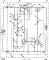
第1図は、本発明による過電圧保護回路を含むバッテリ・パックの概略図である。
第2図は、保護回路の第1代替実施例を示す概略回路図である。
第3図は、保護回路の第2代替実施例を示す概略回路図である。
第4図は、保護回路の第3代替実施例を示す概略回路図である。
好適な実施例の詳細な説明
仕様書は、本発明の新規と見なされる特徴を定義する請求項で締めくくられるが、本発明は以下の説明と図面とを関連づけて考察することにより、さらに良く理解されるものと信じられる。図面においては、同様の参照番号が繰り返し用いられる。
第1図を参照して、ここにはバッテリ・パック10,充電器12および電力を供給される装置14が図示される。バッテリ・パック10は、少なくとも1つのセル16と、保護スイッチ28と、バッテリ電圧および充電器電圧に応答する制御回路26と、バッテリ・セル16がリチウム・イオン・タイプのものである場合は安全スイッチ49とによって構成される。装置に供給される放電電流は、セル16から矢印52の方向に正の装置接触20を通って流れ、負の装置接触24を通って帰還する。セル16は、電流が充電器から矢印54の方向に、正の充電器接触18を通って流れ、負の充電器接触22を通って充電器に帰還すると再充電される。充電器接触18または22のいずれか一方は、電流が充電方向のみに流れ、充電器接触を通じてセルを放電することを防ぐためにダイオード19などの遮断装置を備えることがある。
保護スイッチ28は、ソース46,ドレイン48およびゲート50を有するPチャネル・エンハンスメント・モードMOSFET44によって構成され、ソース46は正の充電器接触18に、ドレイン48はバッテリ・セル16の正の端子15に、ゲート50は比較器出力を有する制御回路26の出力に接続される。すなわち、出力は、高電圧レベルと低電圧レベルとの間で切り替えられる。保護スイッチ28が電流をバッテリ・パック10内に流すと、制御回路26の出力がプルアップ抵抗64を通じて電流を引き込み、電圧を生成してMOSFET44を最も抵抗の低い状態にする。すなわちこれが「オン」である。制御回路26が保護スイッチ28を起動すると、電流はプルアップ抵抗64を通り制御回路26へ、そしてMOSFET44のゲート50に流れ込むのをやめて、それによりMOSFET44からバイアスを除去して、非常に抵抗の高い状態にする。すなわちこれが「オフ」である。この効果は、あたかも電気接触が壊れたようであり、そのために、電流および充電器電圧がバッテリ・セル16と装置14とに印加されなくなる。
バッテリ・セル16としてリチウム・イオン・セルを用いる実施例においては、安全スイッチ49がNチャネル・エンハンスメント・モードMOSFET47によって構成され、バッテリ・セル16と直列に、バッテリ・セルの負の端子17と負の接触22,24との間に配置される。MOSFET47のゲート55は、抵抗51とキャパシタ53とによって形成される遅延回路を通じて制御回路26の出力に接続されるので、MOSFET47は保護スイッチ28がオンまたはオフに対応する状態に切り替わるとすぐにオンまたはオフになる。MOSFETを安全スイッチ49として用いる場合の利点は、装置14が依然として固有ダイオード58により動作することができるということである。この固有ダイオード58は、MOSFET製造の副産物であり、このような装置では周知の特徴である。放電電流は、MOSFET47がオフのときもダイオード58を流れる。スイッチ49がオフのとき、充電器10は、その出力電圧を上げることにより充電を続けようとする。保護スイッチ28がないと、装置14は壊れてしまうことがある。
制御回路26は、反転入力31,非反転入力35および出力36を有する比較器30として構成される演算増幅器によって構成される。電圧基準レッグ33は演算増幅器の非反転入力35に安定した電圧を供給するためのものであり、分圧器レッグ37は演算増幅器の反転入力31に充電器電圧に比例した電圧を供給するためのものである。電圧基準レッグ33は、演算増幅器の非反転入力35と負の充電器接触22との間に接続された電圧基準32と、演算増幅器の非反転入力35のと正の充電器接触18との間に接続された電圧基準バイアス抵抗34とによって構成される。ここでは、正の充電器接触18に接続されて図示されるが、電圧基準バイアス抵抗34は、電圧基準32をバイアスするために充分な電流がそこを流れ安定した電圧を生成する限り、任意の充分に正の値が高い電圧に接続することもできる。
分圧器レッグ37は、負の充電器接触22と演算増幅器の反転入力31との間に接続された第1抵抗38と、演算増幅器の反転入力31の間および保護スイッチ28の両端に夾叉型(straddling configuration)に接続された1対の対向ダイオード40,42の陰極の共通ノード41とに接続された第2抵抗36によって構成される。ダイオード40の陽極は、保護スイッチのソース46に接続され、ダイオード42の陽極は保護スイッチのドレインに接続される。演算増幅器の出力39は、第1比較器出力となり、安全スイッチ49の遅延抵抗51と、駆動トランジスタ57とに接続される。駆動トランジスタ57は、第2比較器出力を供給して保護スイッチ28を制御し、好ましくはNチャネルMOSFETであるが、NPN型バイポーラ・トランジスタ程度の効果があればよい。
夾叉ダイオード40,42は、安全スイッチ49が含まれるバッテリ・パックと共に用いられ、バッテリ・セル16は、リチウム・イオン型または最大充電電圧を有するその他の種類である。ニッケル型バッテリ・システムにおいては、抵抗36はダイオード40の代わりに保護スイッチのソース46に接続してもよい。装置接触20,24を通じてバッテリを充電する充電器があるので、このような充電器により充電されるリチウム・イオン・バッテリは、バッテリ・セル16が安全閾値電圧に到達すると充電電流を中断しなければならない。ダイオード42がなく抵抗36が保護スイッチMOSFET44のソース46に接続される場合は、保護スイッチ28がオフになると、電圧は保護スイッチMOSFET44の固有ダイオード43を通じて分圧器レッグ37に依然として印加される。このため、固有ダイオード43の順方向バイアス電圧誤差により、演算増幅器の反転入力31に印加される電圧が低下する。次に制御回路26がすべてのスイッチを再びオンにして、このサイクルが繰り返され、回路をオンとオフの間で発振させる。ダイオード40,42が図示されるように配置されると、同じ誤差を持つ電圧が、すなわちダイオードの順方向バイアス電圧がいずれか一方のダイオードに印加されるので、この条件は排除される。バッテリが充電器接触18,22を通じて充電された場合、保護スイッチ28がオフになると充電器接触18,22は充電器12が充電を続けようとした場合により高い電圧を提供する。バッテリが装置接触20,24を通じて充電される場合、安全スイッチ49がオフになると、装置接触20,24から同じ誤差を持つ電圧が、あたかも充電器接触18,22からのように分圧器レッグ37に印加される。
バッテリ・パックがどのように動作するかを説明するために、第1図を参照して、バッテリ・セル16の両端の電圧が臨界電圧より低いと想定する。ニッケル型システムにおいては、臨界電圧とは装置が損傷を起こさずに耐えることのできる最大電圧である。リチウム・イオン型システムにおいては、臨界電圧とは、セルの安全閾値電圧であり、1セルにつき約4.3ボルトである。分圧器抵抗38,36は、バッテリ電圧が臨界電圧より低いときに、演算増幅器の反転入力31に供給される電圧が演算増幅器の非反転入力35に供給される電圧基準32の電圧より低くなるように選択される。その結果、演算増幅器の出力39は、以前に定義されたように高電圧になる。これにより保護スイッチ28がオンになり、リチウム・イオン型バッテリでは、安全スイッチ49もオンになる。この間に、すべてのスイッチがオンになるので、充電器12によりセル16に印加される電圧は、装置14に印加される電圧と同じになる。
バッテリ/充電器電圧が臨界電圧に到達すると、分圧器レッグ37抵抗36,38の値は、演算増幅器の反転入力31の電圧が、基準電圧32により演算増幅器の非反転入力35に供給される電圧を少し超えるような値となる。その結果、演算増幅器の出力39は非常に低電圧に切り替わり、これを「低」と呼ぶ。またすべてのスイッチがオフになる。リチウム・イオン型バッテリの場合は、保護スイッチ28がオフになった後で、安全スイッチ49がオフになる。保護スイッチ28がオフになると、充電器接触18,20の両端の電圧は、充電器12の最大出力電圧まで上がり、ダイオード40を通じて分圧器抵抗36,38に印加され、演算増幅器の出力39は低にとどまり、すべてのスイッチはオフのままになる。
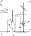
第2図を参照して、第1図に図示されたバッテリ・パック10の第1代替実施例が示される。この実施例においては、保護スイッチ28は、第1図のPチャネル・エンハンスメント・モードMOSFET44の代わりに、少なくとも1つのバイポーラ・トランジスタ、好ましくは2つのトランジスタを備える。ここではトランジスタ70,72と示される。バイポーラ・トランジスタ70のエミッタ74は、正の充電器接触18に接続され、コレクタ76はバッテリ・セル16と正の装置接触20とに接続される。バイポーラ・トランジスタ70のベース78は、バイポーラ・トランジスタ72のエミッタ80に接続される。トランジスタ72のコレクタ82は、トランジスタ70のコレクタに接続される。同一の極性すなわちPNPまたはNPNを有する2つのバイポーラ・トランジスタのこのような配列は、当技術では「ダーリントン構造(darlington configuration)」と呼ばれる。この構造では、有効トランジスタは、エミッタ74,コレクタ76およびベース84を有する。有効トランジスタのベース84は、駆動トランジスタ57に接続される。第2図の実施例は第1図のプルアップ抵抗64を必要としないことを理解されたい。
第1図および第2図において、保護スイッチ28は接触18と20との間に電気的に結合され、これらがバッテリ・パック10の最も正の値が高い側を定義する。この線路は、「高側」とも呼ばれる。充電器12からの電流が、最初は高側線路を介してバッテリ・パック10に入り、セル16に行き、接触22,24により定義される線路により充電器12に帰還する。この第2の線路は、正の値が電気的に最も低く、「低側」と呼ばれる。従って、第1図および第2図の実施例は高側構造(high side configuration)に配列される。
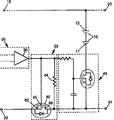
これとは逆に、第3図および第4図では、第1図および第2図に示される保護スイッチは、低側構造(low side configuration)に電気的に結合される。特に第3図においては、MOSFET、特にNチャネルMOSFET60は、接触22,24の間に置かれたソース62とドレイン68とに電気的に結合される。ゲート66は、制御回路26と演算増幅器30の出力と、抵抗64および安全スイッチ49(バッテリ・セル16がリチウム・イオン型である場合)とに電気的に結合される。第4図においても同様に、保護スイッチ28は、低側構造に接続され、少なくとも1つのNPN型バイポーラ・トランジスタである。ただし、ここでは第2図に示されるダーリントン構造の2つのトランジスタ70,72として図示され、有効トランジスタを生成する。保護スイッチ28の低側構造を採用する実施例においては、リチウム・イオン・セルと共に用いられる夾叉ダイオード40,42が、その陽極が共通ノードを形成する分圧器抵抗38と、保護スイッチ28をまたぐその陰極との間に接続され、抵抗36は正の充電接触に接続される。
本発明の好適な実施例が図示および説明されたが、本発明はこれに限定されないことは明白である。添付の請求項により定義されるように、本発明の精神および範囲から逸脱せずに、数多くの修正,変更,変形,置換および等価物が当業者には可能であろう。TECHNICAL FIELD The present invention relates generally to rechargeable batteries, and more particularly to a battery overvoltage protection circuit for a rechargeable battery.
BACKGROUND OF THE INVENTION Complex electronic devices, such as two-way radios, cellular telephones and computers, are becoming increasingly portable as the electronics are integrated into smaller and more efficient integrations. At the same time, there is an increasing demand for better quality battery systems to power portable devices. For devices requiring high power, such as cellular phones and portable computers, rechargeable battery systems, especially nickel-cadmium and nickel metal hydride battery systems, are the most economical options. However, the use of batteries presents interesting challenges to designers of such devices. That is, without the benefit of a regulated power supply, the device must operate at an input voltage range rather than at a particular voltage. Also, the battery voltage keeps changing as the various subsystems of the device turn on and off. Therefore, it is problematic to operate the device consistently while the bias voltage of the electronic part constantly changes.
Of course, the means and knowledge for regulating the battery voltage exist in both the device and the battery itself. An integrated linear voltage regulator that converts the raw battery voltage to a stable voltage for the device can be utilized. However, linear regulators are extremely inefficient, except for the very low current subsystem of the device, given that operating time is a significant feature in the market. Mode switch regulators can be a more efficient means of regulating battery voltage, but cannot be used in low current subsystems due to cost and complexity. Therefore, designers of portable electronic devices must deal with battery voltages that vary as much as 100% from fully discharged to peak voltage during charging.
Since recharging takes an hour or more, it is convenient to allow the device to operate while the battery is being recharged. As a result, the device is exposed to the charger voltage. As mentioned above, the peak voltage required for optimal charging can be quite high. A solution for operating the device efficiently in the operating voltage range of the battery is to ensure that the device is not irreversibly damaged when the charger's peak voltage is applied. This is especially true in handheld communication devices where radio frequency power amplifiers are often connected directly across the raw battery voltage. Intelligent battery system designers avoid this by limiting charger voltage to protect the device, at the expense of charging time as a compromise. However, third party battery charger manufacturers are often unaware of these restrictions, and manufacture and sell chargers that can damage the device. When this occurs, the user may think that the device has failed without noticing that the charger has caused a problem.
Another case where the device is exposed to excessive charger voltage occurs as a result of using lithium-ion batteries. Such cell-based batteries have advantages over nickel-type systems in energy density, and provide users with the advantages of increased operating time, reduced weight, or a combination of both. However, these cells are voltage sensitive and must not be charged above a certain safety threshold voltage for safety reasons. In order to ensure safety, it is necessary to provide a safety switch in series with the cell and interrupt the charging current as necessary. The safety switch is controlled by a circuit that, in response to the cell voltage, activates the safety switch when the cell voltage reaches a safety threshold voltage. This rarely occurs in chargers designed for lithium ion batteries. However, given that many customers are reluctant to buy a new charger just for the purpose of using a lithium-ion battery, the lithium-ion battery is designed to be rechargeable with the existing nickel-type system charger. It is convenient if done. Lithium-ion battery safety switches charged in nickel-type systems are turned off with each recharge cycle. This is because the safe threshold voltage of a lithium ion battery is about two-thirds of the voltage obtained during charging of a nickel battery for the same application. When the safety switch is turned off, the nickel-based system charger raises its output voltage in an attempt to maintain constant current regulation. Since the cell and the safety switch form a series configuration in parallel with the device, the maximum charger voltage is applied to the device that is powered by the battery.
Therefore, in both nickel-type battery systems and, more specifically, lithium-ion batteries, it is necessary to protect the connected devices from excess voltage generated by the receiver when recharging the battery. . Such means should be built into the battery pack so that the battery can be used with any charger.
[Brief description of the drawings]
FIG. 1 is a schematic diagram of a battery pack including an overvoltage protection circuit according to the present invention.
FIG. 2 is a schematic circuit diagram showing a first alternative embodiment of the protection circuit.
FIG. 3 is a schematic circuit diagram showing a second alternative embodiment of the protection circuit.
FIG. 4 is a schematic circuit diagram showing a third alternative embodiment of the protection circuit.
DETAILED DESCRIPTION OF THE PREFERRED EMBODIMENTS While the specification concludes with claims defining the novel features of the present invention, the present invention is better understood upon consideration of the following description and drawings. Is believed to be done. In the drawings, like reference numbers are used repeatedly.
Referring to FIG. 1, a
In an embodiment using a lithium ion cell as the
The
A voltage divider leg 37 includes a first resistor 38 connected between the
The
To illustrate how the battery pack operates, referring to FIG. 1, assume that the voltage across
When the battery / charger voltage reaches the critical voltage, the value of the voltage divider leg 37 resistors 36, 38 is determined by the voltage at the inverting input 31 of the operational amplifier, the voltage supplied to the
Referring to FIG. 2, a first alternative embodiment of the
1 and 2, a
Conversely, in FIGS. 3 and 4, the protection switches shown in FIGS. 1 and 2 are electrically coupled to a low side configuration. In particular, in FIG. 3, a MOSFET, particularly an N-
While the preferred embodiment of the invention has been illustrated and described, it will be clear that the invention is not so limited. Numerous modifications, changes, variations, substitutions and equivalents will occur to those skilled in the art without departing from the spirit and scope of the invention, as defined by the appended claims.
Claims (14)
所定の上限閾値充電電圧を有する少なくとも1つのリチウム・バッテリ・セルと、
前記の充電接触手段と前記少なくとも1つのセルとの間に直列に電気的に接続された保護スイッチ手段と、
前記少なくとも1つのバッテリ・セルと前記負の装置接触との間に直列に電気的に接続された前記スイッチ手段と、
前記安全スイッチ手段に接続され前記少なくとも1つのセルの電圧に応答して前記安全スイッチ手段を起動する第1比較器出力と、前記保護スイッチ手段に接続され前記少なくとも1つのセルの電圧に応答して前記保護スイッチ手段を起動する第2比較器出力とを有する制御回路手段と
を備える再充電可能バッテリ・パック。A charger contact having a positive contact receiving charging current and a negative contact returning the charging current; a positive contact supplying current to the device to supply power to the device and a negative contact receiving current from the device. Rechargeable battery pack comprising: a device contact having a contact, wherein said rechargeable battery pack is recharged through said charging contact means while supplying power to said device through said device contact means. ,
At least one lithium battery cell having a predetermined upper threshold charging voltage;
Protection switch means electrically connected in series between the charging contact means and the at least one cell;
Said switch means electrically connected in series between said at least one battery cell and said negative device contact;
A first comparator output connected to the safety switch means and activating the safety switch means in response to a voltage of the at least one cell; and a first comparator output connected to the protection switch means and responsive to a voltage of the at least one cell. Control circuit means having a second comparator output for activating said protection switch means.
前記ソースが前記の充電接触に電気的に接続され、前記ドレインが前記少なくとも1つのバッテリ・セルに電気的に接続され、前記ゲートが前記制御回路手段の前記第2比較器出力に電気的に接続される
請求項1記載の再充電可能バッテリ・パック。Said protection switch means comprises an enhancement mode MOSFET having a source, a drain and a gate,
The source is electrically connected to the charging contact, the drain is electrically connected to the at least one battery cell, and the gate is electrically connected to the second comparator output of the control circuit means. The rechargeable battery pack of claim 1, wherein
前記エミッタが前記の充電接触手段に電気的に接続され、前記コレクタが前記少なくとも1つのセルに電気的に接続され、前記ベースが前記制御回路手段の前記第2比較器出力に電気的に接続される
請求項1記載の再充電可能バッテリ・パック。Said protection switch means comprises a bipolar transistor having an emitter, a collector and a base,
The emitter is electrically connected to the charging contact means, the collector is electrically connected to the at least one cell, and the base is electrically connected to the second comparator output of the control circuit means. The rechargeable battery pack according to claim 1.
前記エミッタが前記の充電接触手段に電気的に接続され、前記コレクタが前記少なくとも1つのセルに電気的に接続され、前記ベースが前記制御回路手段の前記第2比較器出力に電気的に接続される
請求項1記載の再充電可能バッテリ・パック。Said protection switch means comprises a pair of bipolar transistors arranged in a Darlington configuration to produce a single effective transistor having an emitter, a collector and a base;
The emitter is electrically connected to the charging contact means, the collector is electrically connected to the at least one cell, and the base is electrically connected to the second comparator output of the control circuit means. The rechargeable battery pack according to claim 1.
反転入力、非反転入力および出力を有し、これら前記入力の相対電圧レベルに基づき比較器動作を行う比較器手段であって、前記出力が前記第1比較器出力を提供する比較器手段と、
前記比較器手段の前記非反転入力に基準電圧を提供する電圧基準手段と、
前記バッテリ・パックの電圧に比例する電圧を前記比較器手段の前記反転入力に提供する分圧器手段と
を備える請求項1記載の再充電可能バッテリ・パック。The control circuit comprises:
Comparator means having an inverting input, a non-inverting input and an output, and performing a comparator operation based on a relative voltage level of the inputs, wherein the output provides the first comparator output;
Voltage reference means for providing a reference voltage to the non-inverting input of the comparator means;
Voltage divider means for providing a voltage proportional to the voltage of the battery pack to the inverting input of the comparator means.
前記比較器手段の非反転入力と前記負の接触との間に接続された電圧基準と、
前記電圧基準にバイアス電流を提供し、且つ前記比較器手段の前記非反転入力と正の電圧との間に接続されたバイアス抵抗と
を備える請求項1記載の再充電可能バッテリ・パック。The voltage reference means,
A voltage reference connected between the non-inverting input of the comparator means and the negative contact;
2. The rechargeable battery pack of claim 1, further comprising: providing a bias current to said voltage reference and comprising a bias resistor connected between said non-inverting input of said comparator means and a positive voltage.
前記分圧器手段が、
それぞれ陽極および陰極を有する第1および第2ダイオードであって、前記第1ダイオードの陽極が前記正の充電接触に接続され、前記第2ダイオードの陽極が前記少なくとも1つのセルの前記正の端子に接続され、前記第1および第2ダイオードのそれぞれの前記陰極が共通ノードに接続される、前記第1および第2ダイオードと、
前記比較器手段の前記反転入力と前記少なくとも1つのセルの前記負の端子との間に接続された第1抵抗と、
前記比較器手段の前記反転入力と前記共通ノードとの間に接続された第2抵抗と
を備える請求項12記載の再充電可能バッテリ・パック。The protection switch means is connected to a high-side structure,
Said voltage divider means,
First and second diodes each having an anode and a cathode, wherein the anode of the first diode is connected to the positive charging contact and the anode of the second diode is connected to the positive terminal of the at least one cell. The first and second diodes connected, wherein the respective cathodes of the first and second diodes are connected to a common node;
A first resistor connected between the inverting input of the comparator means and the negative terminal of the at least one cell;
13. The rechargeable battery pack of claim 12, comprising a second resistor connected between the inverting input of the comparator means and the common node.
ゲートと、前記少なくとも1つのバッテリ・セルに接続されたドレインと、前記負の装置接触に接続されたソースとを有するNチャネル・エンハンスメント・モードMOSFETと、
前記Nチャネル・エンハンスメント・モードMOSFETの前記ゲートと前記負の装置接触との間に接続されたキャパシタと、
前記Nチャネル・エンハンスメント・モードMOSFETの前記ゲートと前記制御回路の前記第1比較器出力との間に接続された抵抗と
を備える請求項1記載の再充電可能バッテリ・パック。The safety switch means,
An N-channel enhancement mode MOSFET having a gate, a drain connected to the at least one battery cell, and a source connected to the negative device contact;
A capacitor connected between the gate of the N-channel enhancement mode MOSFET and the negative device contact;
The rechargeable battery pack of claim 1, comprising a resistor connected between said gate of said N-channel enhancement mode MOSFET and said first comparator output of said control circuit.
Applications Claiming Priority (3)
| Application Number | Priority Date | Filing Date | Title |
|---|---|---|---|
| US08/332,166 US5539299A (en) | 1994-10-31 | 1994-10-31 | Protection switch for a battery powered device |
| US08/332,166 | 1994-10-31 | ||
| PCT/US1995/012706 WO1996013890A1 (en) | 1994-10-31 | 1995-10-04 | Protection switch for a battery powered device |
Publications (3)
| Publication Number | Publication Date |
|---|---|
| JPH10508179A JPH10508179A (en) | 1998-08-04 |
| JP3553078B2 true JP3553078B2 (en) | 2004-08-11 |
| JP3553078B6 JP3553078B6 (en) | 2004-11-24 |
Family
ID=
Also Published As
| Publication number | Publication date |
|---|---|
| EP0789947A1 (en) | 1997-08-20 |
| WO1996013890A1 (en) | 1996-05-09 |
| HK1003283A1 (en) | 1998-10-23 |
| JPH10508179A (en) | 1998-08-04 |
| US5539299A (en) | 1996-07-23 |
| DE69518659T2 (en) | 2001-04-19 |
| DE69518659D1 (en) | 2000-10-05 |
| CN1063293C (en) | 2001-03-14 |
| CN1163019A (en) | 1997-10-22 |
| EP0789947A4 (en) | 1997-11-05 |
| EP0789947B1 (en) | 2000-08-30 |
Similar Documents
| Publication | Publication Date | Title |
|---|---|---|
| US5539299A (en) | Protection switch for a battery powered device | |
| JP4031530B2 (en) | Battery pack with undervoltage (UNDER-VOLTAGE) and overvoltage (OVER-VOLTAGE) protection functions | |
| JP3222999B2 (en) | Overdischarge prevention circuit for secondary battery | |
| JP7039773B2 (en) | Power system including battery pack | |
| US6492792B1 (en) | Battery trickle charging circuit | |
| JP3305257B2 (en) | Charge / discharge control circuit, rechargeable power supply device and control method therefor | |
| JP2872365B2 (en) | Rechargeable power supply | |
| KR102247393B1 (en) | Battery pack and method for controlling thereof | |
| JP5488877B2 (en) | Electric tool | |
| JPH11242966A (en) | Protecting method for battery pack and device therefor | |
| US7652450B2 (en) | Secondary battery charging device | |
| JP2005518773A (en) | Hybrid power supply | |
| EP0972327A2 (en) | Battery protection system | |
| JP3747647B2 (en) | Secondary battery protection circuit | |
| US5608307A (en) | Apparatus for controlling excess recharge current applied to a battery | |
| JP3177955B2 (en) | Rechargeable battery charging method and charging system | |
| JP3358559B2 (en) | Low power consumption circuit and secondary battery protection circuit | |
| JP3553078B6 (en) | Protection switch for battery operated devices | |
| JP2799261B2 (en) | Battery charge control device | |
| JP4220660B2 (en) | Method of charging lithium ion secondary battery using solar battery and solar battery type charging device for lithium ion secondary battery | |
| JP2905581B2 (en) | Charging device | |
| KR20150033425A (en) | Auxiliary charging circuit, battery apparatus including the same, and driving method thereof | |
| JP4066584B2 (en) | Temperature detection circuit and charge / discharge circuit | |
| JP3312428B2 (en) | Discharge circuit | |
| JP7522023B2 (en) | Battery pack |
Legal Events
| Date | Code | Title | Description |
|---|---|---|---|
| A521 | Request for written amendment filed |
Free format text: JAPANESE INTERMEDIATE CODE: A523 Effective date: 20040105 |
|
| A911 | Transfer to examiner for re-examination before appeal (zenchi) |
Free format text: JAPANESE INTERMEDIATE CODE: A911 Effective date: 20040122 |
|
| TRDD | Decision of grant or rejection written | ||
| A01 | Written decision to grant a patent or to grant a registration (utility model) |
Free format text: JAPANESE INTERMEDIATE CODE: A01 Effective date: 20040330 |
|
| A61 | First payment of annual fees (during grant procedure) |
Free format text: JAPANESE INTERMEDIATE CODE: A61 Effective date: 20040428 |
|
| R150 | Certificate of patent or registration of utility model |
Free format text: JAPANESE INTERMEDIATE CODE: R150 |
|
| R250 | Receipt of annual fees |
Free format text: JAPANESE INTERMEDIATE CODE: R250 |
|
| FPAY | Renewal fee payment (event date is renewal date of database) |
Free format text: PAYMENT UNTIL: 20090514 Year of fee payment: 5 |
|
| FPAY | Renewal fee payment (event date is renewal date of database) |
Free format text: PAYMENT UNTIL: 20100514 Year of fee payment: 6 |
|
| FPAY | Renewal fee payment (event date is renewal date of database) |
Free format text: PAYMENT UNTIL: 20100514 Year of fee payment: 6 |
|
| FPAY | Renewal fee payment (event date is renewal date of database) |
Free format text: PAYMENT UNTIL: 20110514 Year of fee payment: 7 |
|
| FPAY | Renewal fee payment (event date is renewal date of database) |
Free format text: PAYMENT UNTIL: 20120514 Year of fee payment: 8 |
|
| S533 | Written request for registration of change of name |
Free format text: JAPANESE INTERMEDIATE CODE: R313533 |
|
| FPAY | Renewal fee payment (event date is renewal date of database) |
Free format text: PAYMENT UNTIL: 20120514 Year of fee payment: 8 |
|
| R350 | Written notification of registration of transfer |
Free format text: JAPANESE INTERMEDIATE CODE: R350 |
|
| FPAY | Renewal fee payment (event date is renewal date of database) |
Free format text: PAYMENT UNTIL: 20120514 Year of fee payment: 8 |
|
| RD03 | Notification of appointment of power of attorney |
Free format text: JAPANESE INTERMEDIATE CODE: R3D03 |
|
| FPAY | Renewal fee payment (event date is renewal date of database) |
Free format text: PAYMENT UNTIL: 20120514 Year of fee payment: 8 |
|
| RD04 | Notification of resignation of power of attorney |
Free format text: JAPANESE INTERMEDIATE CODE: R3D04 |
|
| LAPS | Cancellation because of no payment of annual fees |