JP2024516632A - Electronic module for a magnetic switching network for generating pulses of a pulsed output light beam - Google Patents
Electronic module for a magnetic switching network for generating pulses of a pulsed output light beam Download PDFInfo
- Publication number
- JP2024516632A JP2024516632A JP2023565361A JP2023565361A JP2024516632A JP 2024516632 A JP2024516632 A JP 2024516632A JP 2023565361 A JP2023565361 A JP 2023565361A JP 2023565361 A JP2023565361 A JP 2023565361A JP 2024516632 A JP2024516632 A JP 2024516632A
- Authority
- JP
- Japan
- Prior art keywords
- energy storage
- storage node
- additional energy
- network
- electronic
- Prior art date
- Legal status (The legal status is an assumption and is not a legal conclusion. Google has not performed a legal analysis and makes no representation as to the accuracy of the status listed.)
- Pending
Links
Images

Classifications
-
- H—ELECTRICITY
- H01—ELECTRIC ELEMENTS
- H01S—DEVICES USING THE PROCESS OF LIGHT AMPLIFICATION BY STIMULATED EMISSION OF RADIATION [LASER] TO AMPLIFY OR GENERATE LIGHT; DEVICES USING STIMULATED EMISSION OF ELECTROMAGNETIC RADIATION IN WAVE RANGES OTHER THAN OPTICAL
- H01S3/00—Lasers, i.e. devices using stimulated emission of electromagnetic radiation in the infrared, visible or ultraviolet wave range
- H01S3/10—Controlling the intensity, frequency, phase, polarisation or direction of the emitted radiation, e.g. switching, gating, modulating or demodulating
- H01S3/13—Stabilisation of laser output parameters, e.g. frequency or amplitude
- H01S3/131—Stabilisation of laser output parameters, e.g. frequency or amplitude by controlling the active medium, e.g. by controlling the processes or apparatus for excitation
- H01S3/134—Stabilisation of laser output parameters, e.g. frequency or amplitude by controlling the active medium, e.g. by controlling the processes or apparatus for excitation in gas lasers
-
- H—ELECTRICITY
- H01—ELECTRIC ELEMENTS
- H01S—DEVICES USING THE PROCESS OF LIGHT AMPLIFICATION BY STIMULATED EMISSION OF RADIATION [LASER] TO AMPLIFY OR GENERATE LIGHT; DEVICES USING STIMULATED EMISSION OF ELECTROMAGNETIC RADIATION IN WAVE RANGES OTHER THAN OPTICAL
- H01S3/00—Lasers, i.e. devices using stimulated emission of electromagnetic radiation in the infrared, visible or ultraviolet wave range
- H01S3/09—Processes or apparatus for excitation, e.g. pumping
- H01S3/097—Processes or apparatus for excitation, e.g. pumping by gas discharge of a gas laser
- H01S3/09702—Details of the driver electronics and electric discharge circuits
-
- G—PHYSICS
- G03—PHOTOGRAPHY; CINEMATOGRAPHY; ANALOGOUS TECHNIQUES USING WAVES OTHER THAN OPTICAL WAVES; ELECTROGRAPHY; HOLOGRAPHY
- G03F—PHOTOMECHANICAL PRODUCTION OF TEXTURED OR PATTERNED SURFACES, e.g. FOR PRINTING, FOR PROCESSING OF SEMICONDUCTOR DEVICES; MATERIALS THEREFOR; ORIGINALS THEREFOR; APPARATUS SPECIALLY ADAPTED THEREFOR
- G03F7/00—Photomechanical, e.g. photolithographic, production of textured or patterned surfaces, e.g. printing surfaces; Materials therefor, e.g. comprising photoresists; Apparatus specially adapted therefor
- G03F7/20—Exposure; Apparatus therefor
- G03F7/2002—Exposure; Apparatus therefor with visible light or UV light, through an original having an opaque pattern on a transparent support, e.g. film printing, projection printing; by reflection of visible or UV light from an original such as a printed image
- G03F7/2004—Exposure; Apparatus therefor with visible light or UV light, through an original having an opaque pattern on a transparent support, e.g. film printing, projection printing; by reflection of visible or UV light from an original such as a printed image characterised by the use of a particular light source, e.g. fluorescent lamps or deep UV light
-
- G—PHYSICS
- G03—PHOTOGRAPHY; CINEMATOGRAPHY; ANALOGOUS TECHNIQUES USING WAVES OTHER THAN OPTICAL WAVES; ELECTROGRAPHY; HOLOGRAPHY
- G03F—PHOTOMECHANICAL PRODUCTION OF TEXTURED OR PATTERNED SURFACES, e.g. FOR PRINTING, FOR PROCESSING OF SEMICONDUCTOR DEVICES; MATERIALS THEREFOR; ORIGINALS THEREFOR; APPARATUS SPECIALLY ADAPTED THEREFOR
- G03F7/00—Photomechanical, e.g. photolithographic, production of textured or patterned surfaces, e.g. printing surfaces; Materials therefor, e.g. comprising photoresists; Apparatus specially adapted therefor
- G03F7/70—Microphotolithographic exposure; Apparatus therefor
- G03F7/70008—Production of exposure light, i.e. light sources
- G03F7/70025—Production of exposure light, i.e. light sources by lasers
-
- G—PHYSICS
- G03—PHOTOGRAPHY; CINEMATOGRAPHY; ANALOGOUS TECHNIQUES USING WAVES OTHER THAN OPTICAL WAVES; ELECTROGRAPHY; HOLOGRAPHY
- G03F—PHOTOMECHANICAL PRODUCTION OF TEXTURED OR PATTERNED SURFACES, e.g. FOR PRINTING, FOR PROCESSING OF SEMICONDUCTOR DEVICES; MATERIALS THEREFOR; ORIGINALS THEREFOR; APPARATUS SPECIALLY ADAPTED THEREFOR
- G03F7/00—Photomechanical, e.g. photolithographic, production of textured or patterned surfaces, e.g. printing surfaces; Materials therefor, e.g. comprising photoresists; Apparatus specially adapted therefor
- G03F7/70—Microphotolithographic exposure; Apparatus therefor
- G03F7/70008—Production of exposure light, i.e. light sources
- G03F7/70041—Production of exposure light, i.e. light sources by pulsed sources, e.g. multiplexing, pulse duration, interval control or intensity control
-
- G—PHYSICS
- G03—PHOTOGRAPHY; CINEMATOGRAPHY; ANALOGOUS TECHNIQUES USING WAVES OTHER THAN OPTICAL WAVES; ELECTROGRAPHY; HOLOGRAPHY
- G03F—PHOTOMECHANICAL PRODUCTION OF TEXTURED OR PATTERNED SURFACES, e.g. FOR PRINTING, FOR PROCESSING OF SEMICONDUCTOR DEVICES; MATERIALS THEREFOR; ORIGINALS THEREFOR; APPARATUS SPECIALLY ADAPTED THEREFOR
- G03F7/00—Photomechanical, e.g. photolithographic, production of textured or patterned surfaces, e.g. printing surfaces; Materials therefor, e.g. comprising photoresists; Apparatus specially adapted therefor
- G03F7/70—Microphotolithographic exposure; Apparatus therefor
- G03F7/70483—Information management; Active and passive control; Testing; Wafer monitoring, e.g. pattern monitoring
- G03F7/70491—Information management, e.g. software; Active and passive control, e.g. details of controlling exposure processes or exposure tool monitoring processes
- G03F7/70525—Controlling normal operating mode, e.g. matching different apparatus, remote control or prediction of failure
-
- G—PHYSICS
- G03—PHOTOGRAPHY; CINEMATOGRAPHY; ANALOGOUS TECHNIQUES USING WAVES OTHER THAN OPTICAL WAVES; ELECTROGRAPHY; HOLOGRAPHY
- G03F—PHOTOMECHANICAL PRODUCTION OF TEXTURED OR PATTERNED SURFACES, e.g. FOR PRINTING, FOR PROCESSING OF SEMICONDUCTOR DEVICES; MATERIALS THEREFOR; ORIGINALS THEREFOR; APPARATUS SPECIALLY ADAPTED THEREFOR
- G03F7/00—Photomechanical, e.g. photolithographic, production of textured or patterned surfaces, e.g. printing surfaces; Materials therefor, e.g. comprising photoresists; Apparatus specially adapted therefor
- G03F7/70—Microphotolithographic exposure; Apparatus therefor
- G03F7/70483—Information management; Active and passive control; Testing; Wafer monitoring, e.g. pattern monitoring
- G03F7/7055—Exposure light control in all parts of the microlithographic apparatus, e.g. pulse length control or light interruption
-
- H—ELECTRICITY
- H01—ELECTRIC ELEMENTS
- H01S—DEVICES USING THE PROCESS OF LIGHT AMPLIFICATION BY STIMULATED EMISSION OF RADIATION [LASER] TO AMPLIFY OR GENERATE LIGHT; DEVICES USING STIMULATED EMISSION OF ELECTROMAGNETIC RADIATION IN WAVE RANGES OTHER THAN OPTICAL
- H01S3/00—Lasers, i.e. devices using stimulated emission of electromagnetic radiation in the infrared, visible or ultraviolet wave range
- H01S3/10—Controlling the intensity, frequency, phase, polarisation or direction of the emitted radiation, e.g. switching, gating, modulating or demodulating
- H01S3/10007—Controlling the intensity, frequency, phase, polarisation or direction of the emitted radiation, e.g. switching, gating, modulating or demodulating in optical amplifiers
-
- H—ELECTRICITY
- H01—ELECTRIC ELEMENTS
- H01S—DEVICES USING THE PROCESS OF LIGHT AMPLIFICATION BY STIMULATED EMISSION OF RADIATION [LASER] TO AMPLIFY OR GENERATE LIGHT; DEVICES USING STIMULATED EMISSION OF ELECTROMAGNETIC RADIATION IN WAVE RANGES OTHER THAN OPTICAL
- H01S3/00—Lasers, i.e. devices using stimulated emission of electromagnetic radiation in the infrared, visible or ultraviolet wave range
- H01S3/23—Arrangements of two or more lasers not provided for in groups H01S3/02 - H01S3/22, e.g. tandem arrangements of separate active media
- H01S3/2366—Arrangements of two or more lasers not provided for in groups H01S3/02 - H01S3/22, e.g. tandem arrangements of separate active media comprising a gas as the active medium
-
- H—ELECTRICITY
- H01—ELECTRIC ELEMENTS
- H01S—DEVICES USING THE PROCESS OF LIGHT AMPLIFICATION BY STIMULATED EMISSION OF RADIATION [LASER] TO AMPLIFY OR GENERATE LIGHT; DEVICES USING STIMULATED EMISSION OF ELECTROMAGNETIC RADIATION IN WAVE RANGES OTHER THAN OPTICAL
- H01S3/00—Lasers, i.e. devices using stimulated emission of electromagnetic radiation in the infrared, visible or ultraviolet wave range
- H01S3/14—Lasers, i.e. devices using stimulated emission of electromagnetic radiation in the infrared, visible or ultraviolet wave range characterised by the material used as the active medium
- H01S3/22—Gases
- H01S3/223—Gases the active gas being polyatomic, i.e. containing two or more atoms
- H01S3/225—Gases the active gas being polyatomic, i.e. containing two or more atoms comprising an excimer or exciplex
-
- H—ELECTRICITY
- H01—ELECTRIC ELEMENTS
- H01S—DEVICES USING THE PROCESS OF LIGHT AMPLIFICATION BY STIMULATED EMISSION OF RADIATION [LASER] TO AMPLIFY OR GENERATE LIGHT; DEVICES USING STIMULATED EMISSION OF ELECTROMAGNETIC RADIATION IN WAVE RANGES OTHER THAN OPTICAL
- H01S3/00—Lasers, i.e. devices using stimulated emission of electromagnetic radiation in the infrared, visible or ultraviolet wave range
- H01S3/23—Arrangements of two or more lasers not provided for in groups H01S3/02 - H01S3/22, e.g. tandem arrangements of separate active media
- H01S3/2308—Amplifier arrangements, e.g. MOPA
- H01S3/2325—Multi-pass amplifiers, e.g. regenerative amplifiers
- H01S3/2333—Double-pass amplifiers
Landscapes
- Physics & Mathematics (AREA)
- Electromagnetism (AREA)
- Engineering & Computer Science (AREA)
- Plasma & Fusion (AREA)
- Optics & Photonics (AREA)
- General Physics & Mathematics (AREA)
- Microelectronics & Electronic Packaging (AREA)
- Lasers (AREA)
- Charge And Discharge Circuits For Batteries Or The Like (AREA)
- Optical Communication System (AREA)
- Dc-Dc Converters (AREA)
Abstract
機器は、放電チャンバ内の励起機構を起動するように構成された磁気スイッチングネットワークを含む。磁気スイッチングネットワークは、充電器から電流を受け取るように構成された初期エネルギーストレージノード、追加エネルギーストレージノード、及び初期エネルギーストレージノードと追加エネルギーストレージノードとの間の少なくとも1つの電気素子を含む。機器は、追加エネルギーストレージノードに電気的に接続された電子ネットワークも含み、電子ネットワークは、追加エネルギーストレージノードの電圧を制御するように構成される。【選択図】 図5AThe device includes a magnetic switching network configured to activate an excitation mechanism in the discharge chamber. The magnetic switching network includes an initial energy storage node configured to receive current from a charger, an additional energy storage node, and at least one electrical element between the initial energy storage node and the additional energy storage node. The device also includes an electronic network electrically connected to the additional energy storage node, the electronic network configured to control a voltage of the additional energy storage node.
Description
関連出願の相互参照
[0001] 本出願は、「磁気スイッチングネットワーク用の電子モジュール(ELECTRONIC MODULE FOR A MAGNETIC SWITCHING NETWORK)」という名称の、2021年4月28日に出願された米国特許出願第63/180,997号の優先権を主張するものであり、この出願は、参照によりその全体が本明細書に組み込まれる。
CROSS-REFERENCE TO RELATED APPLICATIONS
[0001] This application claims priority to U.S. patent application Ser. No. 63/180,997, filed April 28, 2021, entitled "ELECTRONIC MODULE FOR A MAGNETIC SWITCHING NETWORK," which is incorporated herein by reference in its entirety.
[0002] 本開示は、磁気スイッチングネットワーク用の電子モジュールに関する。磁気スイッチングネットワークは、光学システムにおいて使用され得る。光学システムは、例えば、エキシマレーザであってもよく、又はエキシマレーザを含んでもよく、深紫外(DUV)光を生成してもよい。 [0002] The present disclosure relates to electronic modules for magnetic switching networks. The magnetic switching networks may be used in optical systems. The optical systems may be, or may include, excimer lasers, for example, and may generate deep ultraviolet (DUV) light.
[0003] フォトリソグラフィは、シリコンウェーハなどの基板上に半導体回路をパターン形成するプロセスである。フォトリソグラフィ光学源(又は光源)は、ウェーハ上のフォトレジストを露光するために使用される深紫外(DUV)光を供給する。フォトリソグラフィに使用されるガス放電光源の一種は、エキシマ光源又はレーザとして知られている。エキシマ光源は通常、アルゴン、クリプトン、又はキセノンなどの1つ又は複数の希ガスと、フッ素又は塩素などの反応性ガスとの組み合わせを使用する。エキシマ光源という名称は、電気的刺激(供給エネルギー)及び(ガス混合物の)高圧の適切な条件下で、エキシマと呼ばれる擬似分子が生成され、この擬似分子は通電状態でのみ存在し、紫外領域で増幅された光を生じさせることに由来する。エキシマ光源は、深紫外(DUV)領域の波長を有する光ビームを生成し、この光ビームは、フォトリソグラフィ機器で半導体基板(又はウェーハ)をパターン形成するために使用される。エキシマ光源は、単一のガス放電チャンバを使用して、又は複数のガス放電チャンバを使用して構築することができる。 [0003] Photolithography is the process of patterning semiconductor circuits on a substrate, such as a silicon wafer. A photolithography optical source (or light source) provides the deep ultraviolet (DUV) light used to expose the photoresist on the wafer. One type of gas discharge light source used in photolithography is known as an excimer light source or laser. Excimer light sources typically use a combination of one or more noble gases, such as argon, krypton, or xenon, with a reactive gas, such as fluorine or chlorine. The name excimer light source comes from the fact that under the right conditions of electrical stimulation (supplied energy) and high pressure (of the gas mixture), pseudo-molecules called excimers are created that exist only in an electrically energized state and produce amplified light in the ultraviolet range. Excimer light sources generate a light beam with a wavelength in the deep ultraviolet (DUV) range, which is used to pattern semiconductor substrates (or wafers) in photolithography equipment. Excimer sources can be constructed using a single gas discharge chamber or using multiple gas discharge chambers.
[0004] ある態様では、システムは、パルスシード光ビームを生成するように構成された第1の光学サブシステムであって、第1の気体の利得媒質を保持するように構成された第1のチャンバと、第1のチャンバ内の第1の励起機構と、を含む、第1の光学サブシステムと、パルスシード光ビームに基づいてパルス出力光ビームを生成するように構成された第2の光学サブシステムであって、第2の気体の利得媒質を保持するように構成された第2のチャンバと、第2のチャンバ内の第2の励起機構と、を含む、第2の光学サブシステムと、第1の励起機構を起動するように構成された第1の磁気スイッチングネットワークであって、第1の励起機構を起動することにより、第1の光学サブシステムにパルスシード光ビームのパルスを生成させ、第1の磁気スイッチングネットワークが、第1の初期エネルギーストレージノードと、第1の追加エネルギーストレージノードと、第1の追加エネルギーストレージノードに電気的に接続された第1の磁気スイッチと、第1の初期エネルギーストレージノードと第1の追加エネルギーストレージノードとの間の第1のインダクタと、を含み、第1の初期エネルギーストレージノードが、充電器から電流を受け取るように構成されている、第1の磁気スイッチングネットワークと、第2の励起機構を起動するように構成された第2の磁気スイッチングネットワークであって、第2の励起機構を起動することにより、第2の光学サブシステムにパルス出力光ビームのパルスを生成させ、第2の磁気スイッチングネットワークが、第2の初期エネルギーストレージノードと、第2の追加エネルギーストレージノードと、第2の追加エネルギーストレージノードに電気的に接続された第2の磁気スイッチと、第2の初期エネルギーストレージノードと第2の追加エネルギーストレージノードとの間の第2のインダクタと、を含み、第2の初期エネルギーストレージノードが、充電器から電流を受け取るように構成されている、第2の磁気スイッチングネットワークと、第1の追加エネルギーストレージノード及び第2の追加エネルギーストレージノードに電気的に接続された電子ネットワークであって、電子ネットワークが、第1の追加エネルギーストレージノードと第2の追加エネルギーストレージノードとの間の電圧差を制御するように構成される、電子ネットワークと、を含む。 [0004] In one aspect, a system includes a first optical subsystem configured to generate a pulsed seed light beam, the first optical subsystem including a first chamber configured to hold a first gaseous gain medium and a first excitation mechanism within the first chamber; a second optical subsystem configured to generate a pulsed output light beam based on the pulsed seed light beam, the second optical subsystem including a second chamber configured to hold a second gaseous gain medium and a second excitation mechanism within the second chamber; and a first magnetic switching network configured to activate the first excitation mechanism, whereby activating the first excitation mechanism causes the first optical subsystem to generate pulses of the pulsed seed light beam, the first magnetic switching network including a first initial energy storage node, a first additional energy storage node, a first magnetic switch electrically connected to the first additional energy storage node, and a first inductor between the first initial energy storage node and the first additional energy storage node. The first magnetic switching network includes a first magnetic switching network configured to receive a current from the charger, a second magnetic switching network configured to activate a second excitation mechanism, and activating the second excitation mechanism causes the second optical subsystem to generate pulses of the pulsed output light beam, the second magnetic switching network including a second initial energy storage node, a second additional energy storage node, a second magnetic switch electrically connected to the second additional energy storage node, and a second inductor between the second initial energy storage node and the second additional energy storage node, the second magnetic switching network being configured to receive a current from the charger, and an electronic network electrically connected to the first additional energy storage node and the second additional energy storage node, the electronic network being configured to control a voltage difference between the first additional energy storage node and the second additional energy storage node.
[0005] 実装形態は、以下の特徴の1つ又は複数を含み得る。 [0005] Implementations may include one or more of the following features:
[0006] 電子ネットワークは、第1の追加エネルギーストレージノードと第2の追加エネルギーストレージノードとの間の電圧差を、電圧差を減少させることによって制御するように構成されてもよい。電子ネットワークは、第1の追加エネルギーストレージノードと第2の追加エネルギーストレージノードとの間の電圧差を、電圧差を解消することによって制御するように構成されてもよい。電圧差を解消することは、第1の追加エネルギーストレージノード及び第2の追加エネルギーストレージノードを同じ電圧にすることを含んでもよい。 [0006] The electronic network may be configured to control a voltage difference between the first additional energy storage node and the second additional energy storage node by reducing the voltage difference. The electronic network may be configured to control a voltage difference between the first additional energy storage node and the second additional energy storage node by eliminating the voltage difference. Eliminating the voltage difference may include bringing the first additional energy storage node and the second additional energy storage node to the same voltage.
[0007] 第1の追加エネルギーストレージノードは、第1のエネルギーストレージ装置を含んでもよく、第2の追加エネルギーストレージノードは、第2のエネルギーストレージ装置を含んでもよい。電子ネットワークは、電子ネットワークがアクティブ状態にあるときにのみ、第1の追加エネルギーストレージノードと第2の追加エネルギーストレージノードとの間の電圧差を制御するように構成されてもよく、第1のエネルギーストレージ装置及び第2のエネルギーストレージ装置が電荷を蓄積しているときに、電子ネットワークは、アクティブ状態にあってもよい。電子ネットワークは、電子ネットワークがアクティブ状態にあるときにのみ、第1の追加エネルギーストレージノードと第2の追加エネルギーストレージノードとの間の電圧差を制御するように構成されてもよく、電子ネットワークは、最初の時点でアクティブ状態にあってもよく、電子ネットワークは、最初の時点から既定の時間後にアクティブ状態から遷移してもよい。 [0007] The first additional energy storage node may include a first energy storage device and the second additional energy storage node may include a second energy storage device. The electronic network may be configured to control a voltage difference between the first additional energy storage node and the second additional energy storage node only when the electronic network is in an active state, and the electronic network may be in an active state when the first energy storage device and the second energy storage device are storing charge. The electronic network may be configured to control a voltage difference between the first additional energy storage node and the second additional energy storage node only when the electronic network is in an active state, and the electronic network may be in an active state at an initial time point, and the electronic network may transition out of the active state after a predefined time from the initial time point.
[0008] 電子ネットワークは、アクティブ状態にあるときにのみ、第1の追加エネルギーストレージノードと第2の追加エネルギーストレージノードとの間の電圧差を制御するように構成されてもよく、第1の磁気スイッチングネットワークが第1の励起機構を起動し、第2の磁気スイッチングネットワークが第2の励起機構を起動した後に、電子ネットワークは、アクティブ状態にあってもよく、電子ネットワークは、第1の励起機構の後続の起動前及び第2の励起機構の後続の起動前に、アクティブ状態から遷移してもよい。 [0008] The electronic network may be configured to control a voltage difference between the first additional energy storage node and the second additional energy storage node only when in an active state, the electronic network may be in the active state after the first magnetic switching network activates the first excitation mechanism and the second magnetic switching network activates the second excitation mechanism, and the electronic network may transition out of the active state before a subsequent activation of the first excitation mechanism and before a subsequent activation of the second excitation mechanism.
[0009] 電子ネットワークは、アクティブ状態にあるときにのみ、第1の追加エネルギーストレージノードと第2の追加エネルギーストレージノードとの間の電圧差を制御するように構成されてもよく、電子ネットワークは、第1及び第2の励起機構の各起動の後にアクティブ状態にあり、第1の励起機構及び第2の励起機構の次の起動の前にアクティブ状態から遷移するように構成されてもよい。 [0009] The electronic network may be configured to control a voltage difference between the first additional energy storage node and the second additional energy storage node only when in an active state, and the electronic network may be configured to be in the active state after each activation of the first and second excitation mechanisms and to transition out of the active state before the next activation of the first and second excitation mechanisms.
[0010] 幾つかの実装形態では、第1の追加エネルギーストレージノード及び第2の追加エネルギーストレージノードの各々は、少なくとも1つのキャパシタを含む。 [0010] In some implementations, the first additional energy storage node and the second additional energy storage node each include at least one capacitor.
[0011] 第1の追加エネルギーストレージノードは、第1の磁気スイッチングネットワーク内の複数の追加ストレージノードの1つであってもよく、第2の追加エネルギーストレージノードは、第2の磁気スイッチングネットワーク内の複数の追加ストレージノードの1つであってもよく、システムは、第1の追加ストレージノード以外の第1の磁気スイッチングネットワーク内の追加ストレージノードの1つ、及び第2の追加ストレージノード以外の第2の磁気スイッチングネットワーク内の追加ストレージノードの1つに電気的に接続された第2の電子ネットワークをさらに含む。 [0011] The first additional energy storage node may be one of a plurality of additional storage nodes in the first magnetic switching network, and the second additional energy storage node may be one of a plurality of additional storage nodes in the second magnetic switching network, the system further including a second electronic network electrically connected to one of the additional storage nodes in the first magnetic switching network other than the first additional storage node and to one of the additional storage nodes in the second magnetic switching network other than the second additional storage node.
[0012] 第1の磁気スイッチングネットワーク内の複数の追加ストレージノードの少なくとも1つは、トランスの一次側であってもよく、第2の磁気スイッチングネットワーク内の複数の追加ストレージノードの少なくとも1つは、トランスの一次側であってもよい。 [0012] At least one of the multiple additional storage nodes in the first magnetic switching network may be a primary side of a transformer, and at least one of the multiple additional storage nodes in the second magnetic switching network may be a primary side of a transformer.
[0013] 電子ネットワークは、少なくとも2つのトランジスタを含んでもよい。 [0013] The electronic network may include at least two transistors.
[0014] 電子ネットワークは、複数の制御可能なスイッチを含み、各制御可能なスイッチは、抵抗ネットワークと並列であってもよい。システムは、電子ネットワークと接地との間の接地経路ネットワークも含んでもよい。接地経路ネットワークは、トランジスタ及び抵抗器を含んでもよい。 [0014] The electronic network may include a plurality of controllable switches, each of which may be in parallel with a resistive network. The system may also include a ground path network between the electronic network and ground. The ground path network may include transistors and resistors.
[0015] 電子ネットワークは、第1の追加エネルギーストレージノードと接地との間に電気的に接続された第1の電子ネットワークと、第2の追加エネルギーストレージノードと接地との間に電気的に接続された第2の電子ネットワークと、を含んでもよい。第1の電子ネットワーク及び第2の電子ネットワークの各々は、抵抗素子と直列の電圧制御スイッチを含んでもよい。 [0015] The electronic network may include a first electronic network electrically connected between a first additional energy storage node and ground, and a second electronic network electrically connected between a second additional energy storage node and ground. Each of the first electronic network and the second electronic network may include a voltage controlled switch in series with a resistive element.
[0016] 共振充電器から電流を受け取るように構成された第1の初期エネルギーストレージノード及び第2の初期エネルギーストレージノード。 [0016] A first initial energy storage node and a second initial energy storage node configured to receive current from the resonant charger.
[0017] システムは、第2の電子ネットワークも含んでもよい。第2の電子ネットワークは、第1の初期エネルギーストレージノードに電気的に接続されたダイオードのアノードと、第2の初期エネルギーストレージノードに電気的に接続されたダイオードのアノードとに電気的に接続されてもよい。 [0017] The system may also include a second electronic network. The second electronic network may be electrically connected to an anode of a diode electrically connected to the first initial energy storage node and to an anode of a diode electrically connected to the second initial energy storage node.
[0018] システムは、第2の電子ネットワークも含んでもよい。第2の電子ネットワークは、第1の初期エネルギーストレージノードに電気的に接続されたダイオードのカソードと、第2の初期エネルギーストレージノードに電気的に接続されたダイオードのカソードとに電気的に接続されてもよい。 [0018] The system may also include a second electronic network. The second electronic network may be electrically connected to a cathode of a diode electrically connected to the first initial energy storage node and to a cathode of a diode electrically connected to the second initial energy storage node.
[0019] 第1の磁気スイッチングネットワークは、第1の初期エネルギーストレージノードと第1の追加エネルギーストレージノードとの間の電気接続を制御するように構成された第1のスイッチも含んでもよく、第2の磁気スイッチングネットワークは、第2の初期エネルギーストレージノードと第2の追加エネルギーストレージノードとの間の電気接続を制御するように構成された第2のスイッチも含んでもよい。 [0019] The first magnetic switching network may also include a first switch configured to control an electrical connection between the first initial energy storage node and the first additional energy storage node, and the second magnetic switching network may also include a second switch configured to control an electrical connection between the second initial energy storage node and the second additional energy storage node.
[0020] 第1の磁気スイッチは、第1の可飽和リアクトルを含んでもよく、第2の磁気スイッチは、第2の可飽和リアクトルを含んでもよい。 [0020] The first magnetic switch may include a first saturable reactor, and the second magnetic switch may include a second saturable reactor.
[0021] 別の態様では、機器は、放電チャンバ内の励起機構を起動するように構成された磁気スイッチングネットワークを含む。磁気スイッチングネットワークは、充電器から電流を受け取るように構成された初期エネルギーストレージノード、追加エネルギーストレージノード、及び初期エネルギーストレージノードと追加エネルギーストレージノードとの間の少なくとも1つの電気素子を含む。機器は、追加エネルギーストレージノードに電気的に接続された電子ネットワークであって、追加エネルギーストレージノードの電圧を制御するように構成された電子ネットワークも含む。 [0021] In another aspect, the device includes a magnetic switching network configured to activate an excitation mechanism in the discharge chamber. The magnetic switching network includes an initial energy storage node configured to receive current from a charger, an additional energy storage node, and at least one electrical element between the initial energy storage node and the additional energy storage node. The device also includes an electronic network electrically connected to the additional energy storage node and configured to control a voltage of the additional energy storage node.
[0022] 実装形態は、以下の特徴の1つ又は複数を含み得る。 [0022] Implementations may include one or more of the following features:
[0023] 電子ネットワークは、少なくとも1つの制御可能なスイッチを含んでもよく、制御可能なスイッチは、制御可能なスイッチに電流が流れない第1の状態と、制御可能なスイッチに電流が流れる第2の状態とを含み得る。追加エネルギーストレージノードに電気的に接続されたエネルギーストレージ装置が電荷を受け取っているときに、制御可能なスイッチが第1の状態にあるように制御されてもよい。制御可能なスイッチは、エネルギーストレージ装置が電荷を放電しているときに第2の状態にあるように制御されてもよい。制御可能なスイッチは、追加エネルギーストレージノードに電気的に接続されたエネルギーストレージ装置が閾値量の電荷を受け取った後に、第1の状態にあるように制御されてもよい。制御可能なスイッチは、磁気スイッチングネットワークが励起機構を1回目に起動した後に第1の状態にあるように制御されてもよく、制御可能なスイッチは、磁気スイッチングネットワークが励起機構を2回目に起動する前に第2の状態にあるように制御される。1回目及び2回目は、励起機構の連続した起動であってもよい。幾つかの実装形態では、励起機構の任意の2つの連続する起動の間に、制御可能なスイッチは、第1の状態にあるように制御され、その後、第1の状態から第2の状態に遷移するように制御される。 [0023] The electronic network may include at least one controllable switch, the controllable switch may include a first state in which no current flows through the controllable switch and a second state in which current flows through the controllable switch. The controllable switch may be controlled to be in the first state when an energy storage device electrically connected to the additional energy storage node is receiving charge. The controllable switch may be controlled to be in the second state when the energy storage device is discharging charge. The controllable switch may be controlled to be in the first state after an energy storage device electrically connected to the additional energy storage node receives a threshold amount of charge. The controllable switch may be controlled to be in the first state after the magnetic switching network activates the excitation mechanism a first time, and the controllable switch is controlled to be in the second state before the magnetic switching network activates the excitation mechanism a second time. The first and second times may be successive activations of the excitation mechanism. In some implementations, between any two successive activations of the excitation mechanism, the controllable switch is controlled to be in a first state and then controlled to transition from the first state to a second state.
[0024] 別の態様では、制御システムは、電子ネットワークをトリガするように構成された制御インターフェースを含み、電子ネットワークは、第1の磁気スイッチングネットワーク内の第1のエネルギーストレージノード及び第2の磁気スイッチングネットワーク内の第2のエネルギーストレージノードに電気的に接続されている。第1の磁気スイッチングネットワーク及び第2の磁気スイッチングネットワークの各々は、共振充電器から電荷を受け取る初期エネルギーストレージノードも含む。制御システムは、電子ネットワークにトリガを供給して、電子ネットワークに第1のエネルギーストレージノードを第2のエネルギーストレージノードに電気的に接続させ、第1のエネルギーストレージノードと第2のエネルギーストレージノードとの間の電圧差を減少させるように制御インターフェースに命令するように構成されたスイッチ制御も含む。 [0024] In another aspect, the control system includes a control interface configured to trigger the electronic network, the electronic network electrically connected to a first energy storage node in the first magnetic switching network and a second energy storage node in the second magnetic switching network. Each of the first magnetic switching network and the second magnetic switching network also includes an initial energy storage node that receives charge from the resonant charger. The control system also includes a switch control configured to provide a trigger to the electronic network to cause the electronic network to electrically connect the first energy storage node to the second energy storage node and to instruct the control interface to reduce a voltage difference between the first energy storage node and the second energy storage node.
[0025] 前述のいかなる技法の実装形態も、システム、方法、プロセス、装置、又は機器を含んでもよい。添付図面及び以下の説明において、1つ又は複数の実装形態の詳細を説明する。他の特徴は、説明及び図面から、また特許請求の範囲から明らかになろう。 [0025] Implementations of any of the techniques described above may include systems, methods, processes, apparatus, or devices. Details of one or more implementations are set forth in the accompanying drawings and the description below. Other features will be apparent from the description and drawings, and from the claims.
[0038] 図1Aは、システム100の一例のブロック図である。システム100は、光学源110を含む。光学源110は、半導体ウェーハを露光するために使用される深紫外(DUV)光学源であってもよい。光学源110は、利得媒質119及び励起機構113を封入する放電チャンバ115を含む。励起機構113は、電気パルス155によって起動される。電気パルス155は、スイッチングネットワーク150によって生成される。励起機構113を起動させることにより、利得媒質119において反転分布が生じ、光のパルスが生成される。スイッチングネットワーク150は、光学源110がパルス光ビーム116を生成するように励起機構113に供給される一連の電気パルス155を生成する。
[0038] FIG. 1A is a block diagram of an example of a
[0039] スイッチングネットワーク150は、初期エネルギーストレージノード159、追加エネルギーストレージノード154、及び磁気スイッチ153を含む様々なコンポーネントを含む。初期エネルギーストレージノード159は、充電器142から電気エネルギーを受け取り、蓄える。初期エネルギーストレージノード159は、蓄えられた電気エネルギーを追加ストレージノード154に供給し、追加ストレージノード154は、磁気スイッチ153に電気的に接続される。磁気スイッチ153は、可変インピーダンスを有し、電気パルス155は、磁気スイッチ153のインピーダンスが低いときに生成される。磁気スイッチ153は、例えば可飽和リアクトルであってもよい。
[0039] The
[0040] スイッチングネットワーク150は、追加エネルギーストレージノード154に電気的に接続された電子モジュール170も含む。以下により詳細に説明するように、電子モジュール170は、追加エネルギーストレージノード154における電圧を制御する。追加エネルギーストレージノード154における電圧を制御することにより、システム100及び光学源110の性能が向上する。例えば、追加エネルギーストレージノード154における電圧を制御することにより、磁気スイッチ153の動作点に対する制御をより強化することができ、したがって、電気パルス155の生成のタイミング及びパルス光ビーム116におけるパルスのタイミングに対する強化された制御がもたらされる。
[0040] The
[0041] 図1Bは、スイッチングネットワーク150及びパルス生成ネットワーク152の一例の概略図である。スイッチングネットワーク150は、初期エネルギーストレージノード159(この例ではキャパシタである)、追加エネルギーストレージノード154(この例ではキャパシタである)、インダクタ158、磁気スイッチ153、及び電子モジュール170を含む。初期エネルギーストレージノード159は、充電器142に電気的に接続される。インダクタ158は、初期エネルギーストレージノード159と追加エネルギーストレージノード154との間にある。電子モジュール170は、図1Bの例では追加エネルギーストレージノード154と並列である。
[0041] FIG. 1B is a schematic diagram of an example of a
[0042] 磁気スイッチ153は、磁気コア151を含む。磁気コア151は、外部磁界に曝されることに応答して磁化される任意の材料である。磁気コア151は、例えば、鉄又は鉄合金などの強磁性材料のような、比較的高い透磁率を有する磁性材料であってもよい。透磁率(μ)は、印加された磁界に応答して材料が得る磁化の程度の尺度である。一例として強磁性材料を挙げたが、他の材料が使用されてもよい。
[0042] The
[0043] 図1Bに示す例では、磁気スイッチ153は、磁気コア151を介して制御コイル156及び制御モジュール140に磁気的に結合されている。例えば、制御コイル156は、磁気コア151に巻き付けられるコイル状の電線であってもよい。また、磁気スイッチ153は、磁気コア151に巻き付けられた導電性コイルを含んでいてもよい。制御モジュール140は、バイアス電流を生成する電流源及び/又は電圧源を含んでもよい。バイアス電流は、磁気コア151のインピーダンスを制御するために使用されてもよい。磁気スイッチ153は、制御モジュール140なしで実装されてもよい。
[0043] In the example shown in FIG. 1B, the
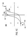
[0044] 図1Cは、磁気コア151の磁化曲線160の一例の図である。図1Cの磁化曲線は、磁界強度(H)の関数としての磁気コア151の磁化(B)のプロットである。磁化(B)の単位はテスラ(T)であり、磁界強度(H)の単位はアンペア毎メートル(A/m)である。任意の特定の時点において、磁気スイッチ153は、その特定の時点における磁化(B)の値と磁界強度(H)の値とによって定義される動作点を有する。
[0044] FIG. 1C is an example diagram of a
[0045] 磁化曲線160は非線形であり、磁気コア151は磁気ヒステリシスを経験する。第1の方向を有する磁界が磁気コア151に印加されると、コア151の材料中の原子双極子が第1の方向とアライメントされ、コア151の材料が第1の方向に磁化される。第1の磁界が除去されると、アライメントの一部が保持される。したがって、外部磁界がない場合(すなわち、H=0の場合)でも、コア151の磁性材料は、ある程度の磁化を保持する。
[0045] The
[0046] 磁気コア151は、順方向飽和領域162及び逆方向飽和領域161を有する。外部磁界の印加によって、もはや磁気コア151の材料の磁化に大きな変化が生じなくなると、磁気コア151は飽和する。磁気コア151のインピーダンスは、領域162及び161で最も低くなる。磁気コア151が飽和しておらず、磁化(B)が領域161と領域162との間にある場合、磁気スイッチ153は、比較的高いインピーダンスを有する。
[0046]
[0047] 再び図1Bを参照すると、充電器142は、高電圧電源141及び共振充電回路135を含む。共振充電回路135は、高電圧電源141の出力ノード133に電気的に接続される。高電圧電源141は、例えば、出力ノード133においてDC900Vを供給可能な32キロワット(kW)電源であってもよい。高電圧電源141は、他の仕様及び特性を有していてもよい。例えば、電源141は、出力ノード133においてDC800Vを供給可能な52kWの電源であってもよい。電源141は、他の電力及び電圧量を供給するように構成されてもよく、電圧及び電力の上記の値は、例として提供されるものである。また、出力ノード133における電圧は、接地に対して正又は負であってもよい。つまり、DC900Vを供給可能な32kW電源の例では、出力ノード133における電圧は、+900V又は-900Vであってもよい。後述の例では、電源141は、負極性を有する。
[0047] Referring again to FIG. 1B, the
[0048] 共振充電回路135は、キャパシタ143、スイッチ148、及びインダクタ144を含む。スイッチ148は、例えば、絶縁ゲートバイポーラトランジスタ(IGBT)などのトランジスタであってもよい。キャパシタ143は、出力ノード133及び接地に電気的に接続される。スイッチ148は、出力ノード133に電気的に接続され、スイッチ148は、インダクタ144と直列である。図1Bに示す共振充電回路135は、一例である。他の実装形態では、共振充電回路135は、例えばダイオード及び追加のスイッチなどの追加のコンポーネントを含んでもよい。さらに他の実装形態では、共振充電回路135の代わりに高電圧キャパシタ充電電源が使用される。
[0048] The
[0049] 高電圧電源141は、キャパシタ143の両端に電圧を印加する。キャパシタ143には電荷が蓄積され、キャパシタ143の両端の電圧は、スイッチ148が閉じるまで増加するか、又は一定のままである。スイッチ148が閉じると、電気パルス生成サイクルが始まる。電気パルス155の1つのインスタンス(及び光ビーム116の対応する1つのパルス)の生成は、電気パルス生成サイクルと呼ばれる。スイッチ148が閉じると、キャパシタ143に蓄えられた電荷が放電され、共振充電回路135の出力ノード134に電気的に接続された初期エネルギーストレージノード159へと流れる。スイッチ148は、キャパシタ143の両端の電圧が指定電圧に達した後に、及び/又は指定時間後に閉じるようにトリガされてもよい。指定電圧値は、指令電圧、事前設定電圧値、又は他の電圧値であってもよい。スイッチ148が閉じた後に、キャパシタ143の電荷が放電される。スイッチ148は、出力ノード134上でターゲット電圧が達成されると開かれる。ターゲット電圧は、例えば、数百ボルト、キャパシタ143の両端の電圧の約2倍の電圧、又はこれらの値の間の電圧であってもよい。
[0049] High
[0050] 幾つかの実装形態では、キャパシタ143は、エネルギーストレージノード159よりもはるかに大きなキャパシタンスを有する。例えば、幾つかの実装形態では、キャパシタ143のキャパシタンスは、キャパシタ159のキャパシタンスよりも少なくとも10倍大きい。キャパシタンスの比較的大きな差により、エネルギーストレージノード159はキャパシタ143の電圧の約2倍まで充電することができる。キャパシタンスの差が大きいことは、キャパシタ143の電圧放電が比較的少ないということでもある。
[0050] In some implementations,
[0051] キャパシタ143からの電荷は、初期エネルギーストレージノード159に蓄積される。初期エネルギーストレージノード159の両端の電圧は、指令電圧まで上昇し、スイッチ145が閉じるまで指令電圧のままである。スイッチ145が閉じると、初期エネルギーストレージノード159に蓄えられた電荷は、初期エネルギーストレージノード159、インダクタ158、及び追加エネルギーストレージノード154によって形成される共振回路に電流(i1)として流れる。図1Dは、時間の関数としての電流(i1)及び電流(i2)の一例を示す。電流(i1)は、時間幅(w1)及び大きさh1を有する。電流(i2)は、時間幅(w2)及び大きさh2を有する。時間幅w1は、インダクタ158、初期エネルギーストレージノード159、及び追加エネルギーストレージノード154の相対インピーダンス値によって決定される。例えば、電流(i1)の時間幅w1は、約5マイクロ秒(μs)であってもよい。時間幅w2は、追加エネルギーストレージノード154、磁気スイッチ153、及びピーキングキャパシタ146の相対インピーダンス値によって決定される。時間幅w2は、例えば500ナノ秒(ns)であってもよい。
[0051] Charge from the
[0052] 電流(i1)が、追加エネルギーストレージノード154から流出し、追加エネルギーストレージノード154の両端の電圧の絶対値が増加する。電流i1の大部分は追加エネルギーストレージノード154から流出するが、磁気スイッチ153にも漏れ電流iLが流入する。磁気スイッチ153に流入する電流は、図1Dでは電流i2として示されている。漏れ電流iLは、コア151の磁化を初期動作点163から経路164(図1C)に沿って増加させ、コア151は、もはや逆方向飽和領域161に存在しない。
[0052] A current (i1) flows out of the additional
[0053] 漏れ電流iLは、磁気スイッチ153に流入し続け、コア151の磁化は、順方向飽和領域162に達するまで経路164に沿って増加し続ける。順方向飽和領域162内にあるとき、コア151のインピーダンスは、ほぼゼロである。この時点で、磁気スイッチ153は、インダクタ158よりも低いインピーダンスを有する。追加エネルギーストレージノード154に蓄えられた電気エネルギーは、電流(図1Dではi2として示されている)として磁気スイッチ153を通って流れ、ピーキングキャパシタ146に蓄積される。これにより、ピーキングキャパシタ146の両端に電位差が形成される。キャパシタ146は、電極113a及び113b(これらは一緒に励起機構113を形成する)と並列である。したがって、キャパシタ146の両端の電位差は、電極113aと電極113bとの間にも形成される。電極113aと電極113bとの間のこの電位差は、利得媒質119を励起する励起パルス155であり、放電チャンバ115(図1A)は、光パルス(光ビーム116のパルス)を放出する。
[0053] The leakage current iL continues to flow into the
[0054] 磁気スイッチ153のインピーダンスは、電流i2が磁気スイッチ153の材料の保磁力(Hc)によって決定される閾値電流値よりも低くなるまで小さいままである。電流i2が磁気スイッチ153を通過すると、電流i2は、もはやコア151に磁界を印加しなくなり、動作点は、経路166に沿って動作点167に移動する。磁気スイッチ153の材料の磁気特性により、経路166は、経路164と同じではない。
[0054] The impedance of
[0055] 上述のように、励起パルス155は、スイッチ153が低インピーダンス状態(例えば、順方向飽和領域162)にあるときに磁気スイッチ153を流れる電流によって生成される。また、磁気スイッチ153の動作点は、追加エネルギーストレージノード154の両端の電圧の絶対値によって影響を受ける。したがって、パルス生成サイクルの開始時に追加エネルギーストレージノード154に存在する電圧の量は、順方向飽和領域162に達するのに必要な時間の量に影響を与え、ひいては、電気パルス155を生成するのに必要な時間の量にも影響を与える。
[0055] As discussed above,
[0056] 追加エネルギーストレージノード154の電圧量は、各電気パルス生成サイクルの開始時に必ずしもゼロではなく、各電気パルス生成サイクルの開始時に必ずしも同じではない。システム100における動作条件は、電気パルス生成サイクルの開始時の追加エネルギーストレージノード154の両端の電圧の量に影響を与え得る。例えば、電気パルス155の反射によって、次の電気パルス生成サイクルの開始前に追加エネルギーストレージノード154の両端に残る残留電圧が生じることがあり、この残留電圧の量は、反射の大きさに依存する。反射の大きさは、利得媒質119の温度及び/又は圧力、電気パルス155の繰返し率及び/又は振幅、及び/又は磁気コア151の温度に基づいて変動し、これらすべては、システム100の動作中に変動し得る。
[0056] The amount of voltage on the additional
[0057] したがって、電気パルス生成サイクルの開始時の追加エネルギーストレージノード154の両端の電圧は、システム100の動作中に変動し得る。電子モジュール170は、追加エネルギーストレージノード154の電圧を制御し、それによって、電気パルス155の生成のタイミングがより制御され、より一貫性があり、及び/又はより予測可能であることが保証される。
[0057] Thus, the voltage across the additional
[0058] さらに、追加エネルギーストレージノード154の両端の電圧を制御することによっても、光学源110のバーストモード性能が向上する。バーストモードで動作する際に、光学源110によって生成される光ビーム116は、光パルスを含まない期間によって分離された光パルスのバーストを含む。各バーストは、数百、数千、数万、又はそれより多い光パルスを含み得る。パルスのバースト内の光パルスは、用途に適した繰返し率を有する。例えば、バースト内の光パルスは、1000ヘルツ(Hz)~6000Hzの繰返し率、又は6000Hzを超える繰返し率を有し得る。バースト間の期間は、バースト内の連続する2つのパルス間の時間よりもはるかに長い持続時間を有する。例えば、あるパルスのバーストの終わりと、次のパルスのバーストとの間の時間は、バースト内の連続する2つのパルス間の時間よりも数百倍から数千倍長い場合がある。バーストの開始時には、放電チャンバ115内の過渡的影響(利得媒質119の温度及び圧力の変化、並びにスイッチングネットワーク150によって生じるスイッチング効果など)によって、最初の数パルス(例えば、最初の100又は200パルス)の光エネルギー量が劇的に変動する。加えて、(図2及び図4に示すような)マルチステージシステムでは、様々なステージ間のタイミング差は、バーストの開始時においてより著しい傾向がある。また、過渡現象の特性は、例えば、励起機構113に印加される電圧、繰返し率、及び利得媒質119の圧力などの動作特性に基づいて変動する。追加エネルギーストレージノード154の両端の電圧を制御すること(及びそれによって、コア151の磁化をより細かく制御すること)によって、バースト過渡効果が低減され得る。
[0058] Additionally, controlling the voltage across the additional
[0059] 図1Bに示す概略図は、一例として提供されるものであり、他の実装形態も可能である。例えば、パルス生成ネットワーク152の例は、1つの磁気スイッチのみを含み、追加エネルギーストレージノード154、磁気スイッチ153、及びピーキングキャパシタ146によって形成される共振回路は、単一の磁気圧縮ステージである。しかし、他の実装形態では、パルス生成ネットワーク152は、追加の磁気圧縮ステージを含む。例えば、パルス生成ネットワーク152は、2つ以上の磁気スイッチ及び2つ以上の磁気圧縮ステージを含み得る。これらの追加の磁気圧縮ステージは、ピーキングキャパシタ146が電極113a及び113bと並列のままであるように、パルス生成回路に配置される。図4は、2つ以上の磁気圧縮ステージを含むスイッチングネットワーク450の一例を示す。
[0059] The schematic diagram shown in FIG. 1B is provided as an example, and other implementations are possible. For example, an example of a pulse-generating
[0060] さらに、システム100は、2つ以上の電子モジュールを含んでもよく、他の電子モジュールは、電子モジュール170と同一であってもよく、又は同一でなくてもよい。例えば、追加の磁気圧縮ステージのうちの1つ又は複数は、電子モジュールに電気的に接続されてもよい。さらに、電子モジュールは、初期エネルギーストレージノード159に電気的に接続されてもよい。
[0060] Additionally,
[0061] また、マルチステージ磁気圧縮回路の任意のバリエーションが使用されてもよい。例えば、磁気圧縮ステージの様々なコンポーネント(例えば、キャパシタ及びインダクタンスコンポーネントの値)は、ピーキングキャパシタ146で生成される電流及び電圧パルスが、他のステージで生成される電圧及び電流よりも短い持続時間及び大きな振幅を有するように選択されてもよい。さらに、パルス生成ネットワーク152は、例えばダイオード及び1つ又は複数の電圧トランスなどの他のコンポーネントを含んでもよい。例えば、パルス生成ネットワーク152は、ピーキングキャパシタ146と並列に昇圧電圧トランスを含んでもよい。昇圧トランスは、ピーキングキャパシタ146の両端の電圧を上昇させ、それによって、より大きな電圧の大きさを有する電気パルスを生成する。昇圧トランスの一例を図4に示す。パルス生成ネットワーク152の具体的な構成にかかわらず、電子モジュール170は、充電器142から直接電荷を受け取らない1つ又は複数のエネルギーストレージノードの電圧を制御するために使用される。
[0061] Also, any variation of a multi-stage magnetic compression circuit may be used. For example, the various components (e.g., capacitor and inductance component values) of the magnetic compression stages may be selected such that the current and voltage pulses generated at the peaking
[0062] 加えて、図1Bに示される例では、高電圧電源141は、出力ノード133における電圧が接地に対して負となるように、負極性を有する電圧を供給する。しかしながら、他の実装形態では、高電圧電源141は、出力ノード133における電圧が接地に対して正となるように、正極性を有する電圧を供給する。高電圧電源141の極性が正である実装形態では、電流(i1)及び(i2)は、図1Bに示されるものとは反対方向に流れる。
[0062] Additionally, in the example shown in FIG. 1B, the high
[0063] 図2は、システム200のブロック図である。システム200は、2ステージレーザシステム210を含む。パルスシード光ビーム216_1を生成する第1の放電チャンバ215_1と、パルスシード光ビーム216_1を増幅して増幅されたパルス光ビーム216_2を生成する第2の放電チャンバ215_2とを含む2ステージレーザシステム。第1の放電チャンバ215_1は、電極213_1a及び213_1bと、気体の利得媒質219_1とを封入し、第2の放電チャンバ215_2は、電極213_2a及び213_2bと、気体の利得媒質219_2とを封入する。
[0063] FIG. 2 is a block diagram of
[0064] システム200は、スイッチングネットワーク250_1及び250_2も含み、これらの各々は、スイッチングネットワーク150(図1A)と類似している。スイッチングネットワーク250_1及び250_2は、それぞれの磁気スイッチ253_1及び253_2(これらのそれぞれは、磁気コアを含む)を含む。スイッチングネットワーク250_1はまた、初期エネルギーストレージノード259_1と、追加エネルギーストレージノード254_1と、追加エネルギーストレージノード254_1に電気的に接続される電子モジュール270_1とを含む。スイッチングネットワーク250_2は、初期エネルギーストレージノード259_2と、追加エネルギーストレージノード254_2と、追加エネルギーストレージノード254_2に電気的に接続された電子モジュール270_2とを含む。
[0064]
[0065] 電子モジュール270_1は、追加エネルギーストレージノード254_1の両端の電圧を制御する。電子モジュール270_2は、追加エネルギーストレージノード254_2の両端の電圧を制御する。幾つかの実装形態では、電子モジュール270_1及び電子モジュール270_2は、追加エネルギーストレージノード254_1の両端の電圧と、追加エネルギーストレージノード254_2の両端の電圧との間の差を制御するように構成される。例えば、電子モジュール270_1及び270_2は、これらの電圧間の差を減らすように、又はこれらの電圧を同じにするように機能するように構成され得る。 [0065] Electronic module 270_1 controls the voltage across additional energy storage node 254_1. Electronic module 270_2 controls the voltage across additional energy storage node 254_2. In some implementations, electronic module 270_1 and electronic module 270_2 are configured to control the difference between the voltage across additional energy storage node 254_1 and the voltage across additional energy storage node 254_2. For example, electronic modules 270_1 and 270_2 can be configured to function to reduce the difference between these voltages or to make these voltages the same.
[0066] システム200は、電子モジュール270_1及び/又は電子モジュール270_2を、モジュール270_1及び270_2が追加エネルギーストレージノード254_1の電圧及び/又は追加エネルギーストレージノード254_2の電圧を制御するアクティブ状態へとトリガするように構成された制御システム230も含む。
[0066]
[0067] スイッチングネットワーク250_1は、電気パルス255_1を生成し、スイッチングネットワーク250_2は、電気パルス255_2を生成する。電気パルス255_1は、利得媒質219_1内の原子、イオン、及び/又は分子を励起して利得媒質219_1において反転分布を生じさせ、シード光ビーム216_1のパルスを生成するのに十分な電位差を電極213_1aと電極213_1bとの間に生成する。シード光ビーム216_1のパルスは、放電チャンバ215_2に入る。電気パルス255_2は、電極213_2bに供給され、電極213_2bと電極213_2aとの間に電位差が形成される。この電位差は、利得媒質219_2中の原子、イオン、及び/又は分子を励起して、利得媒質219_2において反転分布を生じさせるのに十分なものである。放電チャンバ215_2内の励起された利得媒質219_2は、シード光ビーム216_1を増幅し、増幅された光ビーム216_2を放出する。 [0067] Switching network 250_1 generates electrical pulse 255_1, and switching network 250_2 generates electrical pulse 255_2. Electric pulse 255_1 creates a potential difference between electrodes 213_1a and 213_1b sufficient to excite atoms, ions, and/or molecules in gain medium 219_1 to create a population inversion in gain medium 219_1 and create a pulse of seed light beam 216_1. The pulse of seed light beam 216_1 enters discharge chamber 215_2. Electric pulse 255_2 is provided to electrode 213_2b, creating a potential difference between electrodes 213_2b and 213_2a. This potential difference is sufficient to excite atoms, ions, and/or molecules in gain medium 219_2 to create a population inversion in gain medium 219_2. The excited gain medium 219_2 in the discharge chamber 215_2 amplifies the seed light beam 216_1 and emits an amplified light beam 216_2.
[0068] このように、放電チャンバ215-1及び215_2は、増幅された光ビーム216_2を生成するために協働する。したがって、利得媒質219_1及び219_2の励起のタイミングが用途に応じて適切に調整されるように、電気パルス255_1と電気パルス255_2との間の相対的なタイミングに対する制御を維持することが望ましい。例えば、利得媒質219_2は、利得媒質219_1と同時に、又は利得媒質219_1が励起された後の特定の時間に励起されることが期待され得る。媒質219_1の励起と媒質219_2の励起との間の期待されるタイミング又は調整からのずれは、タイミング誤差と呼ばれる。タイミング誤差は、一般に、システム200の性能の低下につながる。例えば、極端な又は大きなタイミング誤差は、利得媒質219_2が励起されていないときに、シード光ビーム216_1のパルスが放電チャンバ215_2を通過することをもたらし得る。この状況では、シード光ビーム216_1のパルスは増幅されない。タイミング誤差がより小さく、極端でない場合も、準最適性能につながることがある。例えば、比較的小さなタイミング誤差は、増幅された光ビーム216_2の様々なパルスの帯域幅及び/又はエネルギーの変動につながる場合がある。また、追加エネルギーストレージノード254_1と追加エネルギーストレージノード254_2との間の小さな電圧差(例えば、約0.1%の差)は、比較的大きなタイミング誤差(例えば、+/-2ナノ秒(ns))をもたらし得る。追加エネルギーストレージノード254_1及び254_2における電圧の量を制御することによって、電子モジュール270_1及び270_2は、放電チャンバ215_1及び放電チャンバ215_2の励起のタイミングが制御され、タイミング誤差が排除、緩和、又は低減されることを保証するのに役立つ。
[0068] In this manner, discharge chambers 215-1 and 215_2 cooperate to generate amplified light beam 216_2. It is therefore desirable to maintain control over the relative timing between electrical pulse 255_1 and electrical pulse 255_2 so that the timing of the excitation of gain mediums 219_1 and 219_2 is appropriately adjusted depending on the application. For example, gain medium 219_2 may be expected to be excited at the same time as gain medium 219_1 or at a particular time after gain medium 219_1 is excited. Any deviation from the expected timing or adjustment between the excitation of medium 219_1 and the excitation of medium 219_2 is referred to as a timing error. Timing errors generally lead to a degradation of the performance of
[0069] 図3は、制御システム330のブロック図である。制御システム330は、制御システム230(図2)として使用されてもよい。制御システム330は、電子処理モジュール331、電子ストレージモジュール332、及び入出力(I/O)インターフェース333を含む。
[0069] FIG. 3 is a block diagram of
[0070] 電子処理モジュール331は、汎用の又は特殊用途のマイクロプロセッサなどの、コンピュータプログラムの実行に適した1つ又は複数のプロセッサ、及び任意の種類のデジタルコンピュータの任意の1つ又は複数のプロセッサを含む。一般的に、電子プロセッサは、読み出し専用メモリ、ランダムアクセスメモリ(RAM)、又はその両方から命令及びデータを受け取る。電子処理モジュール331は、任意の種類の電子プロセッサを含むことがある。電子処理モジュール331の1つ又は複数の電子プロセッサは、命令を実行し、電子ストレージ332に格納されたデータにアクセスする。1つ又は複数の電子プロセッサは、電子ストレージ332にデータを書き込むこともできる。
[0070]
[0071] 電子ストレージ332は、任意のタイプのコンピュータ可読媒体又は機械可読媒体である。例えば、電子ストレージ332は、RAMなどの揮発性メモリであってもよいし、又は不揮発性メモリであってもよい。幾つかの実装形態では、電子ストレージ332は、不揮発性及び揮発性の部分又はコンポーネントを含む。電子ストレージ332は、制御システム330の動作において使用されるデータ及び情報を記憶することができる。電子ストレージ332はまた、制御システム330に、スイッチングネットワーク150(電子モジュール170を含む)、光学源110、及び/又はスキャナ機器(図8A及び図9に示すスキャナ機器880など)内のコンポーネント及びサブシステムと相互作用させる命令(例えば、コンピュータプログラムの形態)を記憶することができる。
[0071]
[0072] 電子ストレージ332は、制御モジュール336を実装する命令及び/又は電子要素も記憶する。制御モジュール336は、電子モジュール170が追加エネルギーストレージノード154の両端の電圧を制御又は調整するように、電子モジュール170をトリガするのに十分なコマンド信号357を生成する。例えば、制御モジュール336は、電圧源を含んでもよい。これらの実装形態において、命令は、電圧信号を生成するように電圧源を制御し、コマンド信号357は、電子モジュール170内のトランジスタに状態を変化させる電圧信号である。また、制御モジュール336は、電子モジュール170内のトランジスタが特定の状態に留まる持続時間を制御するように構成される。電圧信号の大きさ及びタイミングは、事前にプログラムされ、電子ストレージ332に記憶されていてもよい。
[0072]
[0073] システム300は、監視モジュール320も含む。監視モジュール320は、システム100の動作特性を監視可能な任意のタイプの装置である。例えば、監視モジュール320は、繰返し率又は励起機構113に印加される電圧などの動作特性を測定する光学的及び/又は電子的コンポーネントを含み得る。幾つかの実装形態において、監視モジュール320は、光学源110、スイッチングネットワーク150、及び/又は充電器142からの動作特性の値にアクセスする。これらの実装形態において、監視モジュール320は、動作特性を直接測定しない。例えば、監視モジュール320は、直接測定を行う他のセンサ(温度若しくは圧力センサ、又はパルスタイミング誤差センサなど)から読取値を取得してもよく、及び/又は製造時に設定され、光学源110の特定のサブシステム内のメモリに記憶された設定値を取得してもよい。
[0073] The system 300 also includes a
[0074] 幾つかの実装形態では、監視モジュール320によって収集された情報は、電子モジュール170をいつトリガするかを決定するために使用される。例えば、監視モジュール320は、光ビーム116の繰返し率を測定してもよく、制御システム330は、予め指定された数の光パルスが生成された後に、電子モジュール170をトリガしてもよい。
[0074] In some implementations, information collected by the
[0075] 電子ストレージ332は、レーザコマンドモジュール337を構成する命令も記憶する。レーザコマンドモジュール337は、光学源110及び/又はパルス生成ネットワーク152の動作の様々な態様を制御する。レーザコマンドモジュール337は、例えば、スイッチ148及び145の状態を制御する。幾つかの実装形態では、コマンドモジュール337は、スイッチ148を閉じることによってパルス生成サイクルを開始し、出力ノード134上でターゲット電圧が達成されたときに開くようにスイッチ148に命令する。ターゲット電圧の値は、電子ストレージ322に記憶されてもよく、及び/又はI/Oインターフェース333を介してオペレータ又は機械から受信されてもよい。他の実装形態も可能である。例えば、レーザコマンドモジュール337は、共振充電器135のキャパシタ143の両端の電圧が指定電圧に達した後に、又は所定の時間が経過した後に、スイッチ148を閉じるようにトリガするように構成されてもよい。レーザコマンドモジュール337は、キャパシタ159の両端の電圧が指定電圧に達した後に、スイッチ145を閉じるようにトリガする。例えば、スイッチ148及び145がトランジスタである実装形態では、レーザコマンドモジュール337は、トランジスタのゲートに電圧を供給する電圧源を制御することができ、この電圧は、トランジスタに状態を変化させ、電流を導通させるのに十分なものである。指定電圧及び所定の時間は、電子ストレージ332に記憶される。
[0075]
[0076] レーザコマンドモジュール337はまた、光ビーム116の繰返し率などの光学源110の他の態様を制御してもよい。レーザコマンドモジュール337は、電子ストレージ332に記憶され、及び/又はI/Oインターフェース333を介して提供される事前にプログラムされた処方に基づいて、様々な態様を制御することができる。
[0076]
[0077] 電子ストレージ332はまた、光学源110及び/又はパルス生成ネットワーク152の動作に使用される様々な他のパラメータ及び値を記憶してもよい。
[0077]
[0078] I/Oインターフェース333は、制御システム330が、オペレータ、他の装置(監視モジュール320など)、及び/又は別の電子装置上で実行されている自動化プロセスとデータ及び信号を交換することを可能にする、任意の種類のインターフェースである。例えば、電子ストレージ332に記憶された規則又は命令を編集することができる実装形態では、編集は、I/Oインターフェース333を介して行われることがある。別の例において、幾つかの実装形態では、システム100のオペレータ又はユーザは、I/Oインターフェース333を使用して、制御モジュール336に電子モジュール170をトリガさせることができる。I/Oインターフェース333は、視覚ディスプレイ、キーボード、並びにパラレルポート、ユニバーサルシリアルバス(USB)接続、及び/又は例えばイーサネットなどの任意のタイプのネットワークインターフェースなどの通信インターフェースのうちの1つ又は複数を含み得る。I/Oインターフェース333は、例えば、IEEE802.11、Bluetooth、又は近距離無線通信(NFC)接続を通じて、物理的な接触なしでの通信を可能にすることもできる。
[0078] The I/
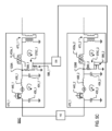
[0079] 図4は、スイッチングネットワーク450の概略図である。スイッチングネットワーク450は、図2及び図9に示す光学システムなどの2ステージ光学システムと共に使用されるスイッチングネットワークの一例である。スイッチングネットワーク450は、電子モジュール470a_1、470b_1、470a_2、及び470b_2も含み、これらは、様々なエネルギーストレージノード(図4の例ではキャパシタ)の電圧レベルを制御するために使用される。スイッチングネットワーク450は、充電器142及び制御システム330と共に使用される。スイッチングネットワーク450は、第1のコミュテータ471_1及び第1の圧縮ヘッド472_1を含み、これらは、分離された電極413_1の第1のセット間に電位差を生じさせる電気パルス455_1を生成する。電極413_1は、第1の気体の利得媒質も含む第1の放電チャンバ内に封入される。スイッチングネットワーク450は、第2のコミュテータ471_2及び第2の圧縮ヘッド472_2も含み、これらは、分離された電極413_2の第2のセット間に電位差を生じさせる電気パルス455_2を生成する。分離された電極413_2は、気体の利得媒質も封入する第2の放電チャンバ内に封入される。
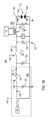
4 is a schematic diagram of a
[0080] 充電器142は、キャパシタ459_1と、スイッチ445_1のエミッタとに電気的に接続されている。この例では、スイッチ445_1は、絶縁バイポーラゲートトランジスタ(IGBT)である。スイッチ445_1のゲートは、電圧源(図示せず)に結合されている。充電器142がトリガされてオンになると、電流がキャパシタ459_1に流れる。キャパシタ459_1の両端の電圧が指定電圧を達成すると、スイッチ445_1がトリガされてオン状態に変化し、電流がスイッチ445_1及びインダクタ458_1を通って流れ、キャパシタ454_1に蓄積される。電流i1の一部は、磁気スイッチ453a_1にも漏れ、コア451a_1の磁化は、順方向飽和点に達するまで増加する。キャパシタ454_1内の電気エネルギーは、磁気スイッチ453a_1を通って流れ、昇圧電圧トランス473_1によって、より高い電圧に変換され、キャパシタ474_1に蓄積される。図4に示す実装形態は昇圧電圧トランス473_1を示しているが、入力電圧に対して出力電圧を上昇させることができる任意の装置が使用され得る。磁気コア451b_1が順方向飽和領域162に入る。キャパシタ474_1に蓄えられた電気エネルギーは、磁気スイッチ453b_1を通って流れ、ピーキングキャパシタ446_1に蓄積され、第1の電極413_1のペア間に電位差を生じさせる。昇圧電圧トランス473_1によって提供される電圧の上昇により、比較的大きな電圧がピーキングキャパシタ446_1の両端に形成されることが可能となる。例えば、充電器142がキャパシタ459_1に電気的に接続された出力ノードにおいて約DC800Vを供給する実装形態では、ピーキングキャパシタ446_1上の電圧の絶対値は、約20kVであり得る。
[0080] The
[0081] 第2のコミュテータ471_2及び第2の圧縮ヘッド472_2も同様に動作する。 [0081] The second commutator 471_2 and the second compression head 472_2 operate in a similar manner.
[0082] スイッチングネットワーク450は、電子モジュール470a_1、470b_1、470a_2、及び470b_2も含む。電子モジュール470a_1は、キャパシタ454_1と並列に電気的に接続されている。電子モジュール470b_1は、キャパシタ474_1と並列に電気的に接続されている。電子モジュール470a_2は、キャパシタ454_2と並列に電気的に接続されている。電子モジュール470b_2は、キャパシタ474_2と並列に電気的に接続されている。電子モジュール470a_1、470b_1、470a_2、及び470b_2の各々は、制御可能な電子ネットワークを含む。制御可能な電子ネットワークは、例えば、1つ又は複数のトランジスタ又は他の制御可能な電子装置を含み得る。電子モジュール470a_1は、キャパシタ454_1の両端の電圧を制御する。電子モジュール470b_1は、キャパシタ474_1の両端の電圧を制御する。電子モジュール470a_2は、キャパシタ454_2の両端の電圧を制御する。電子モジュール470b_2は、キャパシタ474_2の両端の電圧を制御する。
[0082] The
[0083] スイッチングネットワーク450は、図4に示されていない追加の要素を含んでいてもよい。例えば、スイッチングネットワーク450は、初期エネルギーストレージノード(この例ではキャパシタ459_1及びキャパシタ459_2)に接続された電子モジュールを含んでもよい。電子モジュールは、ダイオードを含んでもよい。(図4に示すような)初期エネルギーストレージノードの負極性電荷に基づく実装形態の場合、ダイオードは、アノードが初期エネルギーストレージノードに接続された状態で配置される。初期エネルギーストレージノードの正極性電荷に基づく実装形態の場合、ダイオードは、カソードが初期エネルギーストレージノードに接続された状態で配置される。これらの電子モジュールは、初期エネルギーストレージノードの電圧を制御するように機能する。
[0083] The
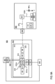
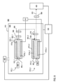
[0084] 図5A~5Cは、電子モジュールの例を含む概略図である。図5Aを参照すると、スイッチングネットワーク550Aは、第1のコミュテータ571_1及び第2のコミュテータ571_2を含む。スイッチングネットワーク550Aは、追加の磁気圧縮ステージを含み得る。例えば、スイッチングネットワーク550Aは、第1の圧縮ヘッド472_1及び第2の圧縮ヘッド472_2(図4)を含んでもよい。第1のコミュテータ571_1及び第2のコミュテータ571_2は、第1のコミュテータ571_1が電子モジュール470_1を含まず、第2のコミュテータ571_1が電子モジュール470_2を含まないことを除いて、第1のコミュテータ471_1及び第2のコミュテータ471_2(図4)と同じである。その代わりに、スイッチングネットワーク550Aは、ノード529A及びノード529Bの電圧を制御するように構成された電子モジュール570Aを含む。ノード529Aの電圧は、キャパシタ454_1の両端の電圧であり、ノード529Bの電圧は、キャパシタ454_2の両端の電圧である。例えば、電子モジュール570Aは、ノード529Aとノード529Bとの間の電圧差を低減又は除去するように構成されてもよい。つまり、電子モジュール570Aは、ノード529A及びノード529Bの電圧を同じにするように構成されてもよい。
5A-5C are schematic diagrams including examples of electronic modules. Referring to FIG. 5A, a
[0085] 電子モジュール570Aは、第1の高電圧スイッチ581_1、第2の高電圧スイッチ581_2、並びに抵抗器583_1及び583_2を含む。抵抗器583_1及び583_2は、同じ抵抗値を有してもよい。第1及び第2の高電圧スイッチ581_1及び581_2は、スイッチが電流を導通するオン状態と、スイッチが電流を導通しないオフ状態とを少なくとも含む任意のタイプの制御可能なスイッチである。スイッチ581_1及び581_2は、例えば、金属酸化膜電界効果トランジスタ(MOSFET)、バイポーラ接合トランジスタ(BJT)、又はIGBTなどのトランジスタであってもよい。図5Aに示す例では、各高電圧スイッチ581_1及び581_2は、MOSFETである。スイッチ581_1のソースは、ノード529Aに電気的に接続されている。スイッチ581_1のゲートは、制御システム330に電気的に接続されている。スイッチ581_1のドレインは、スイッチ581_2のドレインに電気的に接続されている。スイッチ581_2のゲートは、制御システム300に電気的に接続されている。スイッチ581_2のソースは、ノード529Bに電気的に接続されている。抵抗器583_1は、スイッチ581_1と並列であり、抵抗器583_2は、スイッチ581_2と並列である。
[0085]
[0086] 電子モジュール570Aは、スイッチ581_1及び581_2がオン状態のときにノード529A及び529Bの低インピーダンス短絡を提供し、スイッチがオフ状態のときにノード529Aとノード529Bとの間の高インピーダンス接続を提供するように構成される。スイッチ581_1及び581_2がオフのときは、スイッチ581_1及び581_2に実質的に電流が流れず、コミュテータ571_1及び571_2は、抵抗器583_1及び583_2を介してのみ電気的に接続される。抵抗器583_1及び583_2は、ノード529Aとノード529Bとの間に高インピーダンス経路を提供する。スイッチ581_1及び581_2がオンの場合に、電流は、ノード529Aからスイッチ581_1に流れ、ノード529Bからスイッチ581_2に流れる。これにより、ノード529A及び529Bの電圧が平衡化されるか、又は同じ電圧値に向かって変化し、それによって、ノード529Aとノード529Bとの間の電圧差の大きさが減少し、及び/又はノード529A及び529Bの電圧が同じになる。
[0086]
[0087] 電子モジュール570Aは、スイッチ581_1及び581_2がオンの場合に、アクティブ状態にあるか、又は有効化されている。電子モジュール570Bは、スイッチ581_1及び581_2がオフの場合に、非アクティブ状態にあるか、又は無効化されている。制御システム330は、トリガ信号を用いてスイッチ581_1及び581_2の状態を制御する。例えば、スイッチ581_1及び581_2をオンにするために、制御システム330は、スイッチ581_1のゲート及びスイッチ581_2のゲートに電圧信号を供給する。電圧の特性(例えば、振幅及び極性)は、スイッチの仕様に依存するが、トリガ電圧は、スイッチ581_1及び581_2をオン状態に遷移させるのに十分なものである。制御システム330は、スイッチ581_1及び581_2をオフにするようにも構成される。例えば、スイッチ581_1及び581_2がMOSFETである実装形態では、制御システム330は、ソースの電圧よりも小さいトリガ信号をスイッチ581_1及び581_2のそれぞれのゲートに供給する。
[0087]
[0088] 図5Bは、スイッチングネットワーク550Bの概略図である。スイッチングネットワーク550Bは、スイッチングネットワーク550Bが電子モジュール570Aの代わりに電子モジュール570Bを含むことを除いて、スイッチングネットワーク550Aと同じである。電子モジュール570Bは、制御可能なスイッチ584_1、584_2、及び584_3を含む。電子モジュール570Aは、スイッチ584_1、581_2、及び581_3がオン状態のときに接地への低インピーダンス経路を提供し、これらのスイッチがオフ状態のときに高インピーダンスを提供するように構成される。ノード529A及び529Bは、電子モジュール570Bが非アクティブ状態のときに、抵抗器585_1及び585_2を介してのみ電気的に接続される。
[0088] FIG. 5B is a schematic diagram of switching
[0089] 高電圧スイッチ584_1、584_2、及び584_3は、スイッチが電流を導通する低インピーダンス経路を提供するオン状態と、スイッチが電流を導通しない高インピーダンスを提供するオフ状態とを少なくとも含む任意のタイプの制御可能なスイッチである。スイッチ584_1、584_2、及び584_3は、例えば、金属酸化膜電界効果トランジスタ(MOSFET)、バイポーラ接合トランジスタ(BJT)、又はIGBTなどのトランジスタであってもよい。図5Aに示す例では、各高電圧スイッチ584_1、584_2、及び584_3は、MOSFETである。スイッチ584_1のソースは、ノード529Aに電気的に接続されている。スイッチ584_1のゲートは、制御システム330に電気的に接続されている。スイッチ584_1のドレインは、スイッチ584_2のドレインに電気的に接続されている。スイッチ584_2のゲートは、制御システム300に電気的に接続されている。スイッチ584_2のソースは、ノード529Bに電気的に接続されている。抵抗器585_1は、スイッチ581_1と並列であり、抵抗器585_2は、スイッチ581_2と並列である。抵抗器585_1及び585_2は、同じ抵抗値を有していてもよい。
[0089] High voltage switches 584_1, 584_2, and 584_3 are any type of controllable switch that includes at least an on state in which the switch provides a low impedance path for conducting current, and an off state in which the switch provides a high impedance for not conducting current. Switches 584_1, 584_2, and 584_3 may be transistors, such as metal oxide field effect transistors (MOSFETs), bipolar junction transistors (BJTs), or IGBTs. In the example shown in FIG. 5A, each high voltage switch 584_1, 584_2, and 584_3 is a MOSFET. The source of switch 584_1 is electrically connected to
[0090] 電子モジュール570Bは、スイッチ584_3及び抵抗器585_3も含む。スイッチ584_3のゲートは、制御システム330に接続されている。スイッチ584_3のソースは、抵抗器585_1と585_2との間に電気的に接続されている。スイッチ584_3のドレインは、接地に接続されている。抵抗器585_3は、抵抗器585_1と抵抗器585_2との間に接続され、且つスイッチ584_3のソースと直列に電気的に接続されている。電子モジュール570Bは、抵抗器585なしで実装されてもよい。電子モジュール570Bが直列抵抗器585_3を含むか否かにかかわらず、スイッチ584_3がオン状態にあるときに、スイッチ584_3は、接地経路に抵抗を提供する。一方、直列抵抗器585_3を含むことにより、接地経路のインピーダンスの制御をより強化することができる。
[0090]
[0091] 電子モジュール570Bは、スイッチ584_1、584_2、及び584_3がオンの場合に、アクティブ状態にあるか、又は有効化されている。電子モジュール570Bは、スイッチ584_1、584_2、及び584_3がオフの場合に、非アクティブ状態にあるか、又は無効化されている。電子モジュール570Bは、電子モジュール570Bがアクティブである場合に、各ノード529A及びノード529Bと接地との間に低インピーダンス経路を提供する。電子モジュール570Bがアクティブ状態にある場合に、ノード529A上及びノード529B上の電荷は、抵抗器585_3及びスイッチ584_3を介して接地へと放電される。これにより、ノード529Aとノード529Bとの間の電圧差が減少し、又は解消され、ノード529A及びノード529Bの各々の電位が減少し、又は解消される。電子モジュール570Bが非アクティブ状態にある場合に、電子モジュール570Bがノード529A又はノード529Bにおける電圧に実質的に影響を与えないように、電子モジュール570Bは、ノード529Aとノード529Bとの間に高インピーダンス経路を形成する。
[0091]
[0092] 電子モジュール570A(図5A)及び570B(図5B)は、コミュテータ571_1及び571_2の両方に接続される外部モジュールである。図5Cは、内部電子モジュール570C_1及び570C_2の一例を示す。内部電子モジュール570C_1又は570C_2は、電子モジュール170又は270として使用することができる。
[0092]
[0093] 電子モジュール570C_1は、抵抗器589_1と、抵抗器589_1と直列であるスイッチ586_1とを含む。スイッチ586_1は、任意のタイプの制御可能なスイッチであり、例えば、トランジスタであってもよい。図5Cの例では、スイッチ586_1は、MOSFETである。抵抗器589_1は、ノード529A及びスイッチ586_1のソースに電気的に接続されている。電子モジュール570C_2は、抵抗器589_2と、抵抗器589_2と直列のスイッチ586_2とを含む。スイッチ586_2は、任意のタイプの制御可能なスイッチであり、例えば、トランジスタであってもよい。図5Cの例では、スイッチ586_2は、MOSFETである。抵抗器589_2は、ノード529B及びスイッチ586_2のソースに電気的に接続されている。スイッチ586_1及び586_2の各々のドレインは、接地に接続されている。スイッチ586_1及び586_2の各々のゲートは、制御システム330に接続されている。制御システム330は、それぞれのゲートにトリガ信号を供給することによって、スイッチ586_1及び586_2の状態を制御する。すなわち、制御システム330は、スイッチ586_1がオンであるか、或いはオフであるかを判定し、及びスイッチ586_2がオンであるか、或いはオフであるかを判定する。
[0093] Electronic module 570C_1 includes resistor 589_1 and switch 586_1 in series with resistor 589_1. Switch 586_1 may be any type of controllable switch, for example, a transistor. In the example of FIG. 5C, switch 586_1 is a MOSFET. Resistor 589_1 is electrically connected to
[0094] スイッチ586_1がオンの場合、電子モジュール570C_1は、アクティブ状態にあるか、又は有効化されており、ノード529A上の電荷は、電子モジュール570C_1を介して接地に放電される。スイッチ586_1がオフの場合、電子モジュール570C_1は、ノード529Aに対して高インピーダンスを示し、ノード529Aの電圧に影響を与えない。同様に、スイッチ586_2がオンの場合、電子モジュール570C_2は、アクティブ状態にあり、ノード529B上の電荷が接地へと放電される。スイッチ586_2がオフの場合、電子モジュール570C_2は、ノード529Bに対して高インピーダンスを示し、ノード529Bの電圧に影響を与えない。
[0094] When switch 586_1 is on, electronic module 570C_1 is in an active state, or enabled, and the charge on
[0095] 図5A~5Cに示す例では、電子モジュール570A、570B、及び570Cは、ノード529A及び529Bの電圧を制御するために使用される。しかしながら、他の実装形態も可能である。例えば、電子モジュール570A、570B、及び570Cは、昇圧トランス473_1及び473_2(図4)などの他のエネルギーストレージノードに接続されてもよい。また、システムは、電子モジュール570A、570B、570C_1、及び/又は570C_2のうちの2つ以上を含んでもよい。例えば、システムは、電子モジュール570Aがノード529A及び529Bに接続され、電子モジュール570Aの第2のインスタンスがキャパシタ474_1及び474_2に接続された状態で実装されてもよい。
5A-5C,
[0096] 図6及び図7は、それぞれ、エネルギーストレージノードの電圧を制御する電子モジュールを含むスイッチングネットワークを動作させるための、例示的なプロセス600及び700のフローチャートである。例えば、プロセス600及び700は、スイッチングネットワーク150、250、450、550A、550B、又は550Cと共に使用されてもよい。プロセス600及び700は、電子ストレージ332に記憶され、制御システム330の電子処理モジュール331によって実行される実行可能命令の一群又はコンピュータプログラムとして実装されてもよい。プロセス600は、スイッチングネットワーク550B(図5B)及び制御システム300に関して説明されている。しかしながら、プロセス600は、1つ又は複数のエネルギーストレージノードに電子モジュールを含む他のスイッチングネットワークを用いて実行されてもよい。
6 and 7 are flow charts of example processes 600 and 700, respectively, for operating a switching network including an electronic module that controls the voltage of an energy storage node. For example, processes 600 and 700 may be used with switching
[0097] 図6を参照すると、電子モジュール570Bが無効化される(610)。電子モジュール570Bを無効化するために、制御システムのコマンドモジュール336(図3)は、コマンド信号357のインスタンスを各スイッチ584_1、584_2、及び584_3のゲートに発行する。コマンド信号357は、各スイッチ584_1、584_2、及び584_3をオフ状態にするのに十分な電圧信号である。コマンド信号357の特性は、スイッチ584_1、584_2、及び584_3の仕様に依存する。例えば、スイッチ584_1、584_2、及び584_3がpチャネルMOSFETである場合、コマンド信号357は、ゲートとソースとの間の電圧をゼロより大きくする電圧信号である。電子モジュール570Bが無効化された状態では、ノード529A及び529Bは、互いに電気的に分離されている。
[0097] Referring to FIG. 6,
[0098] 電気パルス生成サイクルが開始される(620)。上述したように、電気パルス生成サイクルにより、電極413_1と電極413_2(図4)との間に電位差が形成される。電気パルス生成サイクルの間、電子モジュール570Bは無効化される。したがって、電子モジュール570Bは、エネルギーストレージノード454_1又はエネルギーストレージノード454_2に蓄積される電荷に影響を与えない。加えて、電子モジュール570Bは、蓄積された電荷の可飽和リアクトル453a_1及び453a_2への放電に影響を与えない。電気パルス455_1及び455_2が生成される(630)。
[0098] An electrical pulse generation cycle is initiated (620). As described above, the electrical pulse generation cycle creates a potential difference between electrodes 413_1 and 413_2 (FIG. 4). During the electrical pulse generation cycle,
[0099] 制御システム330は、電子モジュール570Bを有効化する(640)。例えば、制御システム330は、電気パルス455_1及び455_2が生成された後であって、後続の電気パルスが生成される前に、蓄積された電荷が後続の電気パルスが生成される前にエネルギーストレージノード529A及び529Bから除去されるように、電子モジュール570Bを有効化することができる。制御システム330は、スイッチ584_1、584_2、及び584_3をオン状態にトリガすることによって、電子モジュール570Bを有効化する。電子モジュール570Bは、スイッチ584_1、584_2、及び584_3をオンにするのに十分な特性を有する電圧信号を各スイッチ584_1、584_2、及び584_3のゲートに供給することができる。例えば、スイッチ584_1、584_2、及び584_3がpチャネルMOSFETである場合、制御システム330は、ゲートとソースとの間の電圧がゼロ未満となるような電圧信号を各スイッチ584_1、584_2、及び584_3のゲートに供給する。電子モジュール570Bを有効化することにより、ノード529A及び529Bから電荷が放散され、ノード529A及び529Bが同じ電圧を有するようになる。
[0099] The
[0100] 制御システム300が(640)で電子モジュール570Bを有効化した後に、プロセス600は終了するか、又は(610)に戻る場合がある。幾つかの実装形態において、プロセス650は、条件チェック(650)を含む。これらの実装形態において、制御システム330は、事前設定条件が満たされたか否かを判定する(650)。事前設定条件が満たされていない場合、制御システム330は、電子モジュール570Bと相互作用せず、電子モジュール570Bは、条件が満たされるまで、(エネルギーストレージノード529A及び529Bが電気的に接続され、電荷がノード529A及び529Bから放散されるように)有効化状態のままである。事前設定条件が満たされた場合、プロセス600は、(610)に戻り、電子モジュール570Bは、(エネルギーストレージノード529A及び529Bが互いに電気的に接続されないように)無効化される。
[0100] After the control system 300 enables the
[0101] 条件(650)を含む実装形態において、事前設定条件は、例えば、電気パルス455_1及び455_2の生成の完了と、電極413a_1及び413a_2、並びに電極413b_1及び413b_2の結果として生じる励起とであってもよい。これらの実装形態において、プロセス600は、電気パルス455_1及び455_2の生成が完了した後にのみ(610)に戻る。この事前設定条件は、電子モジュール570Bが電気パルス455_1及び455_2を生成した電気パルス生成サイクルを妨害しないこと、並びにそれぞれの電気パルス455_1及び455_2の反射によりノード529A及び529B上に生じ得る残留電荷が次の電気パルス生成サイクルを妨害しないことを保証する(電子モジュール570Bは、ノード529A及び529Bから電荷を放散するために(640)で有効化されたため)。このように、事前設定条件は、電気パルス生成サイクルの開始時に、エネルギーストレージノード529A及び529Bの状態が予測可能であり、及び一定であることを保証するのに役立つ。
[0101] In implementations that include condition (650), the preset condition may be, for example, the completion of generation of electrical pulses 455_1 and 455_2 and the resulting excitation of electrodes 413a_1 and 413a_2 and electrodes 413b_1 and 413b_2. In these implementations, process 600 returns to (610) only after generation of electrical pulses 455_1 and 455_2 is complete. This preset condition ensures that
[0102] 事前設定条件の別の例は、時間間隔である。時間間隔は、例えば、電気パルス生成サイクルの開始時からの一定時間、電子モジュール570Bが有効化された後の一定時間、又は電極413a_1及び413a_2の励起、及び/又は電極413b_1及び413b_2の励起後の一定時間であってもよい。時間間隔は、電子ストレージ332に記憶されてもよい。
[0102] Another example of a pre-set condition is a time interval. The time interval may be, for example, a fixed time from the start of an electrical pulse generation cycle, a fixed time after
[0103] プロセス600は、各電気パルス生成サイクルの開始時に実行されてもよい。これらの実装形態では、プロセス600は、パルスごとに実行され、電極413a_1及び413b_1を含む第1のチャンバと、電極413a_2及び413b_2を含む第2のチャンバとを含む2ステージ光学システムによって生成される光の各パルスに対して実行される。つまり、これらの実装形態において、電子モジュール570Bは、各パルス生成サイクルの開始時に無効化され(610)、各パルス生成サイクルの完了後に有効化され(640)、プロセス600が条件(650)を含む場合、条件(650)は、1つのパルス生成サイクルの完了である。他の実装形態では、プロセス600は、2ステージ光学システムによって生成されるパルスの各バーストの前に実行される。さらに他の実装形態では、プロセス600は、2ステージ光学システムによって生成される幾つかの光パルス(ただしすべての光パルスではない)の前に実行される。
[0103] Process 600 may be performed at the beginning of each electrical pulse generation cycle. In these implementations, process 600 is performed on a pulse-by-pulse basis, for each pulse of light generated by a two-stage optical system including a first chamber including electrodes 413a_1 and 413b_1 and a second chamber including electrodes 413a_2 and 413b_2. That is, in these implementations,
[0104] また、幾つかの実装形態では、起動時、すなわち設置若しくは修理後の最初の使用時、光パルスのバーストの開始時、又は任意の他の比較的長期の非アクティブ状態の期間(及び電子モジュール570Bの直近の有効化からの長期の期間)の後に、制御システム330は、非アクティブ状態の間にノード529A及び529Bに蓄積された可能性のある残留電圧が、プロセス600を実行する前に放電されるように、(610)で電子モジュール570Bを無効化する前に、電子モジュール570Bを有効化してもよい。
[0104] Also, in some implementations, upon start-up, i.e., first use after installation or repair, at the beginning of a burst of light pulses, or after any other relatively long period of inactivity (and long periods since the most recent activation of
[0105] 図7を参照すると、プロセス700は、スイッチングネットワークを動作させるためのプロセスの別の例である。プロセス700は、スイッチングネットワーク550A(図5A)及び制御システム300に関して説明される。しかしながら、プロセス700は、1つ又は複数のエネルギーストレージノードに電子モジュールを含む他のスイッチングネットワークを用いて実行されてもよい。
[0105] Referring to FIG. 7, process 700 is another example of a process for operating a switching network. Process 700 is described with respect to switching
[0106] 電子モジュール570Aは、ノード529A及び529Bの電圧を平衡化させるために有効化される(710)。電子モジュール570Aは、制御システム330によって有効化される。例えば、制御システム330は、スイッチ581_1及び581_2がオンになるように、各スイッチ581_1及び581_2のゲートに電圧信号を供給してもよい。電子モジュール570Aを有効化することにより、ノード529Aの電圧とノード529Bの電圧との間の差が減少し、又は解消される。電気パルス生成サイクルが開始される(720)。キャパシタ454_1及び454_2は、図4に関して上述したように電荷を蓄積する。電子モジュール570Aは、キャパシタ454_1及び454_2が電荷を蓄積している間、ノード529A及び529Bにおける電圧を平衡化又は均等化させるように機能する。モジュール570Aは、可飽和リアクトル453a_1及び453a_2が飽和する前、並びにキャパシタ454_1及び454_2が電気エネルギーを放電する前に、無効化される(730)。電子モジュール570Aを無効化するために、制御システム330は、スイッチ581_1及び581_2のそれぞれのゲートに電圧信号を供給し、スイッチをオフにする。モジュール570Aが無効化された後、ノード529A及び529Bは、抵抗器583_1及び583_2を介してのみ電気的に接続される。上述したように、電気パルス455_1及び455_2が生成される(740)。
[0106]
[0107] 電気パルス455_1及び455_2が(740)で生成された後、プロセス700は、(710)に戻る。プロセス700は、各電気パルス生成サイクルの開始時に実行されてもよい。これらの実装形態において、プロセス700は、パルスごとに実行され、電極413a_1及び413b_1を含む第1のチャンバと、電極413a_2及び413b_2を含む第2のチャンバとを含む2ステージ光学システムによって生成される光の各パルスに対して実行される。他の実装形態では、プロセス700は、2ステージ光学システムによって生成されるパルスの各バーストの前に実行される。さらに他の実装形態では、プロセス700は、2ステージ光学システムによって生成される幾つかの光パルス(ただしすべての光パルスではない)の前に実行される。 [0107] After electrical pulses 455_1 and 455_2 are generated at (740), process 700 returns to (710). Process 700 may be performed at the beginning of each electrical pulse generation cycle. In these implementations, process 700 is performed on a pulse-by-pulse basis and for each pulse of light generated by a two-stage optical system including a first chamber including electrodes 413a_1 and 413b_1 and a second chamber including electrodes 413a_2 and 413b_2. In other implementations, process 700 is performed before each burst of pulses generated by the two-stage optical system. In still other implementations, process 700 is performed before some (but not all) of the light pulses generated by the two-stage optical system.
[0108] プロセス700は、パルス生成サイクルが始まる前に、キャパシタ454_1及び454_2の電圧を平衡化させる。したがって、パルス生成サイクルの開始前にキャパシタ454_1及び454_2上の電圧が異なる場合(例えば、そのような電圧差は、前のパルスに起因する場合がある)、電子モジュール570Aを有効化することにより、キャパシタ454_1及び454_2上の電圧が平衡化され、タイミング誤差を引き起こす可能性のある電圧誤差が緩和される。さらに、パルス生成サイクルが始まる前に電子モジュール570Aを有効化することによって、充電回路135(これは充電器142の一部である)に起因する電圧差の原因が緩和され、したがって、タイミング誤差が低減又は解消される。充電回路135に起因する電圧差の原因の例として、ターンオン時間、充電回路135における損失又は電圧降下の差が挙げられる。
[0108] Process 700 balances the voltages of capacitors 454_1 and 454_2 before a pulse generation cycle begins. Thus, if the voltages on capacitors 454_1 and 454_2 are different before a pulse generation cycle begins (e.g., such voltage differences may be due to a previous pulse), enabling
[0109] 図8A及び図9は、上述した技法を使用することができるシステムのさらなる例を提供する。 [0109] Figures 8A and 9 provide further examples of systems that can use the techniques described above.
[0110] 図8Aは、深紫外(DUV)光学システム800の一例である。システム800は、露光ビーム(又は出力光ビーム)816をスキャナ機器880に供給する光生成モジュール810を含む。図8Aの例では、光生成モジュール810は、スイッチングネットワーク150と共に使用される。制御システム805も、光生成モジュール810及び光生成モジュール810に関連する様々なコンポーネントに結合される。
[0110] FIG. 8A is an example of a deep ultraviolet (DUV)
[0111] 光生成モジュール810は、光発振器812を含む。光発振器812は、出力光ビーム816を生成する。光発振器812は、放電チャンバ815を含み、この放電チャンバは、励起機構(カソード813-a及びアノード813-b)を封入している。放電チャンバ815は、気体の利得媒質819(図8Aでは、薄い点線の網掛けで示されている)も含む。カソード813-aとアノード813-bとの間の電位差によって、気体の利得媒質819中に電界が形成される。この電位差は、電極813-aと電極813-bとの間に電位差を生成するようにスイッチングネットワーク150を制御することによって生成される。この電位差は、電界を形成し、この電界は、反転分布を引き起こし、誘導放出によって光のパルスの生成を可能にするのに十分なエネルギーを利得媒質819に供給する。
[0111] The light-generating
[0112] このような電位差を繰り返し生成することによって、光ビーム816として放出される一連のパルスが形成される。パルス光ビーム816の繰返し率は、電極813-a及び813-bに電圧が印加される率によって決定される。パルスの繰返し率は、例えば、約500~6,000ヘルツ(Hz)に及び得る。他の繰返し率が使用されてもよく、光生成モジュール810は、単一の光パルスが放出されるシングルショットモードで動作されてもよい。幾つかの実装形態では、この繰返し率は、6,000Hzより大きくてもよく、例えば、12,000Hz以上であってもよい。光発振器812から放出される各パルスは、例えば、約1ミリジュール(mJ)のパルスエネルギーを有していてもよい。
[0112] By repeatedly generating such a potential difference, a series of pulses is formed that are emitted as
[0113] また、光ビーム816は、光のない間隔によって区切られた光のパルスのバーストを含み得る。バーストは、数百又は数千の光のパルスを含み得る。バースト内で、光のパルスは、電位差が電極813-aと電極813-bとの間に形成される率によって決定される繰返し率を有する。バースト間の時間は、用途によって決定され、例えば、バースト内の2つの連続するパルス間の時間よりも100倍又は1000倍長くてもよい。
[0113]
[0114] 気体の利得媒質819は、用途に必要とされる波長、エネルギー、及び帯域幅において光ビームを生成するのに適した何れかのガスでもよい。気体の利得媒質819は、2つ以上のタイプのガスを含んでもよく、この様々なガスはガス成分と呼ばれる。エキシマ放射源では、気体の利得媒質819は、例えばアルゴン、キセノン、若しくはクリプトンなどの貴ガス(希ガス)、又は、例えばフッ素若しくは塩素などのハロゲンを含んでもよい。ハロゲンが利得媒質である実装形態においては、利得媒質はまた、ヘリウムなどのバッファガスは別にして、キセノンの痕跡を含む。
[0114] The
[0115] 気体の利得媒質819は、深紫外(DUV)の範囲内の光を放出する利得媒質でもよい。DUV光は、例えば、約100ナノメートル(nm)~約400nmの波長を含んでもよい。気体の利得媒質819の具体例には、約193nmの波長で光を放出するフッ化アルゴン(ArF)、約248nmの波長で光を放出するフッ化クリプトン(KrF)、又は約351nmの波長で光を放出する塩化キセノン(XeCl)が含まれる。
[0115] The
[0116] 共振器が、放電チャンバ815の一方の側にあるスペクトル調整装置895と、放電チャンバ815の第2の側にある出力カプラ896との間に形成される。スペクトル調整装置895は、例えば、放電チャンバ815のスペクトル出力を微調整する回折格子及び/又はプリズムなどの回折光学部品を含むことがある。回折光学部品は、反射型又は屈折型であり得る。一部の実装形態では、スペクトル調整装置895は、複数の回折型光学素子を含む。例えば、スペクトル調整装置895は4つのプリズムを含むことがあり、それらのプリズムのうちの幾つかは光ビーム816の中心波長を制御するように構成され、他のものは光ビーム816のスペクトル帯域幅を制御するように構成される。
[0116] A resonator is formed between a
[0117] 光ビーム816のスペクトル特性は、他の方法で調整されることがある。例えば、光ビーム816のスペクトル帯域幅及び中心波長などのスペクトル特性は、チャンバ815の気体の利得媒質の圧力及び/又はガス濃度を制御することにより、調整されることがある。光生成モジュール810がエキシマ放射源である実装形態の場合、光ビーム816のスペクトル特性(例えば、スペクトル帯域幅又は中心波長)は、チャンバ815内の、例えばフッ素、塩素、アルゴン、クリプトン、キセノン、及び/又はヘリウムの圧力及び/又は濃度を制御することにより、調整されることがある。
[0117] The spectral characteristics of the
[0118] 気体の利得媒質819の圧力及び/又は濃度は、ガス供給システム890を用いて制御可能である。ガス供給システム890は、流体導管889を介して放電チャンバ815の内部に流体結合されている。流体導管889は、流体の損失なく又は最小限の損失を伴って、ガス又は他の流体を運ぶことができる任意の導管である。例えば、流体導管889は、流体導管889内で運ばれている1種又は複数種の流体と反応しない材料でできているか又はコーティングされているパイプであり得る。ガス供給システム890は、利得媒質819で使用される1種又は複数種のガスを含むか及び/又はガスの供給を受け取るように構成されるチャンバ891を含む。ガス供給システム890は、ガス供給システム890が放電チャンバ815からのガスを除去するか又は放電チャンバ815へガスを注入できるようにするデバイス(ポンプ、弁、及び/又は流体スイッチなど)も含む。ガス供給システム890は、制御システム805に結合されている。
[0118] The pressure and/or concentration of the
[0119] 光発振器812はまた、スペクトル解析機器898を備える。スペクトル解析機器898は、光ビーム816の波長を測定又は監視するのに使用されてもよい測定システムである。図8Aに示す例では、スペクトル解析機器898は、出力カプラ896からの光を受光する。
[0119] The
[0120] 光生成モジュール810は、他の構成要素及びシステムを備えてもよい。例えば、光生成モジュール810は、ビーム準備システム899を備えてもよい。このビーム準備システム899は、パルスストレッチャと相互作用する各パルスを時間的に引き伸ばすパルスストレッチャを備えてもよい。ビーム準備システムはまた、例えば、反射型及び/又は屈折型の光学素子(たとえば、レンズやミラーなど)、及び/又はフィルタなど、光に作用することのできる他の構成要素を備えてもよい。図に示す例では、ビーム準備システム899は、露光ビーム816の経路内に配置される。しかし、ビーム準備システム899は、システム800内の他の場所に配置されてもよい。
[0120] The
[0121] システム800はまた、スキャナ機器880を備える。スキャナ機器880は、所要形状に作られた露光ビーム816Aでウェーハ882を露光する。所要形状に作られた露光ビーム816Aは、投影光学システム881を通して、露光ビーム816を通過させることによって形成される。スキャナ機器880は、液浸システム又は乾式システムでもよい。スキャナ機器880は、ウェーハ882に到達する前に露光ビーム816が通過する投影光学システム881、及びセンサシステム又は計測システム870を備える。ウェーハ882は、ウェーハホルダ883上で保持され又は受けられる。スキャナ機器880はまた、例えば、温度制御装置(空気調和装置及び/又は加熱装置など)、及び/又は様々な電気構成部品用の電源を備えてもよい。
[0121] The
[0122] 計測システム870は、センサ871を備える。センサ871は、例えば、帯域幅、エネルギー、パルス持続時間、及び/又は波長など、所要形状に作られた露光ビーム816Aの特性を測定するように構成されてもよい。センサ871は、例えば、ウェーハ882における所要形状に作られた露光ビーム816Aの画像を取り込むことのできるカメラ若しくは他の装置でもよく、又は、x-y平面でのウェーハ882における光エネルギーの量を示すデータを取り込むことのできるエネルギー検出器でもよい。
[0122]
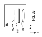
[0123] また図8Bを参照すると、投影光学システム881は、スリット884と、マスク885と、レンズシステム886を含む投影対物レンズとを備える。レンズシステム886は、1つ又は複数の光学素子を備える。露光ビーム816は、スキャナ機器880に入り、スリット884に衝突し、出力光ビーム816の少なくとも一部が、スリット884を通過して、所要形状に作られた露光ビーム816Aを形成する。図8A及び図8Bの例では、スリット884は長方形であり、露光ビーム816を、細長い長方形状に作られた光ビームに成形し、これが所要形状に作られた露光ビーム816Aになる。マスク885は、所要形状に作られた光ビームのどの部分がマスク885によって透過され、どの部分がマスク885によって遮断されるかを決定するパターンを含む。ウェーハ882上の輻射線感応性フォトレジスト材料の層を、露光ビーム816Aで露光することによって、ウェーハ882上に超小型電子機能が形成される。マスク上のパターンのデザインは、所望の具体的な超小型電子回路機能によって決定される。
[0123] Also referring to FIG. 8B, the projection
[0124] 図8Aに示す構成は、DUVシステムにおける構成の一例である。他の実装形態も実現可能である。例えば、光生成モジュール810は、光発振器812のN個の具体例を含んでもよく、ここで、Nは2以上の整数である。こうした実装形態では、各光発振器812は、露光ビーム816を形成するビーム結合器に向けてそれぞれの光ビームを放出するように構成される。
[0124] The configuration shown in FIG. 8A is one example of a configuration in a DUV system. Other implementations are possible. For example,
[0125] 図9には、DUVシステムの例示的な別の構成が示してある。図9は、スキャナ機器880に供給されるパルス状の光ビーム916を生成する光生成モジュール910を備える、フォトリソグラフィシステム900のブロック図である。制御システム805は、システム900の様々な動作を制御するために、光生成モジュール910の様々なコンポーネント及びスキャナ機器880に結合されている。光生成モジュール910は、スイッチングネットワーク450と共に使用される。
[0125] Another exemplary configuration of a DUV system is shown in FIG. 9. FIG. 9 is a block diagram of a
[0126] 光生成モジュール910は、シード光ビーム918を電力増幅器(PA)912_2に提供する主発振器(MO)912_1を含む、2ステージレーザシステムである。PA912_2は、MO912_1からシード光ビーム918を受け取り、シード光ビーム918を増幅して、スキャナ機器880で使用するための光ビーム916を生成する。例えば、実装形態によっては、MO912_1は、1パルスあたり約1ミリジュール(mJ)のシードパルスエネルギーを有するパルスシード光ビームを放射することがあり、これらのシードパルスは、PA912_2によって約6~15mJまで増幅されることがあるが、他の実施例では他のエネルギーが使用されてよい。
[0126] The
[0127] MO912_1は、2つの細長い電極913a_1及び913b_1、ガス混合物である利得媒質919_1(図9に明るい点線の網掛けで示す)、並びに電極913a_1と913b_1との間でガス混合物を循環させるためのファン(図示せず)を有する、放電チャンバ915_1を含む。共振器が、放電チャンバ915_1の一方の側にあるライン狭隘化モジュール995と、放電チャンバ915_1の第2の側にある出力カプラ996との間に形成される。
[0127] MO912_1 includes a discharge chamber 915_1 having two elongated electrodes 913a_1 and 913b_1, a gain medium 919_1 that is a gas mixture (shown in FIG. 9 with light dotted shading), and a fan (not shown) for circulating the gas mixture between electrodes 913a_1 and 913b_1. A resonator is formed between a
[0128] 放電チャンバ915_1は、第1のチャンバ窓963_1及び第2のチャンバ窓964_1を含む。第1のチャンバ窓963_1及び第2のチャンバ窓964_1は、放電チャンバ915_1の両側にある。第1のチャンバ窓963_1及び第2のチャンバ窓964_1は、DUV範囲内の光を透過し、DUV光が放電チャンバ915_1に出入りするのを可能にする。 [0128] Discharge chamber 915_1 includes a first chamber window 963_1 and a second chamber window 964_1. The first chamber window 963_1 and the second chamber window 964_1 are on opposite sides of discharge chamber 915_1. The first chamber window 963_1 and the second chamber window 964_1 transmit light in the DUV range and allow DUV light to pass into and out of discharge chamber 915_1.
[0129] ライン狭隘化モジュール995は、放電チャンバ915_1のスペクトル出力を微調整する回折格子又はプリズム(図9Aに示すような)などの回折光学部品Sを含むことがある。光生成モジュール910は、出力カプラ996から出力光ビームを受け取るライン中心分析モジュール968、及びビーム結合光学システム969も含む。ライン中心分析モジュール968は、シード光ビーム918の波長を測定又は監視するのに使用されることがある測定システムである。ライン中心分析モジュール968は、光生成モジュール910内の他の場所に配置されることがあるか、又は、光生成モジュール910の出力部に配置されることがある。
[0129] The
[0130] 利得媒質919_1であるガス混合物は、用途に必要とされる波長及び帯域幅で光ビームを生成するのに適した任意のガスであり得る。エキシマ放射源の場合、ガス混合物は、例えば、アルゴン若しくはクリプトンなどの貴ガス(希ガス)、例えばフッ素若しくは塩素などのハロゲン、及びヘリウムなどの緩衝ガスとは別の微量のキセノンを含むことがある。ガス混合物の具体的な例としては、約193nmの波長で光を放射するフッ化アルゴン(ArF)、約248nmの波長で光を放射するフッ化クリプトン(KrF)、又は約351nmの波長で光を放射する塩化キセノン(XeCl)が挙げられる。したがって、この実装形態では、光ビーム916及び918は、DUV範囲内の波長を含む。エキシマ利得媒質(ガス混合物)は、細長い電極913a_1、913b_1に電圧を印加することにより、高電圧放電で、短い(例えばナノ秒の)電流パルスを伴ってポンピングされる。 [0130] The gas mixture that is the gain medium 919_1 can be any gas suitable for generating a light beam at the wavelength and bandwidth required for the application. In the case of an excimer radiation source, the gas mixture may include, for example, a noble gas such as argon or krypton, a halogen such as fluorine or chlorine, and a trace amount of xenon apart from a buffer gas such as helium. Specific examples of gas mixtures include argon fluoride (ArF), which emits light at a wavelength of about 193 nm, krypton fluoride (KrF), which emits light at a wavelength of about 248 nm, or xenon chloride (XeCl), which emits light at a wavelength of about 351 nm. Thus, in this implementation, the light beams 916 and 918 include wavelengths in the DUV range. The excimer gain medium (gas mixture) is pumped with short (e.g., nanosecond) current pulses in a high-voltage discharge by applying a voltage to the elongated electrodes 913a_1, 913b_1.
[0131] PA912_2は、MO912_1からシード光ビーム918を受け取り、シード光ビーム918を放電チャンバ915_2を通してビーム回転光学素子992に向ける、ビーム結合光学システム969を含み、ビーム回転光学素子992は、シード光ビーム918が放電チャンバ915_2に送り返されるにように、シード光ビーム918の方向を修正又は変更する。ビーム回転光学素子992及びビーム結合光学システム969は、循環する閉ループの光路を形成し、この光路では、リング増幅器への入力が、ビーム結合光学システム969においてリング増幅器の出力と交差する。
[0131] PA912_2 includes a beam combining
[0132] 放電チャンバ915_2は、一対の細長い電極913a_2、913b_2、利得媒質919_2(図9では、薄い点線の網掛けで示されている)、及び電極913a_2と電極913b_2との間で利得媒質919_2を循環させるためのファン(図示せず)を含む。利得媒質919_2を形成するガス混合物は、利得媒質919_1を形成するガス混合物と同じであってもよい。 [0132] Discharge chamber 915_2 includes a pair of elongated electrodes 913a_2, 913b_2, a gain medium 919_2 (shown in FIG. 9 with light dotted shading), and a fan (not shown) for circulating gain medium 919_2 between electrodes 913a_2 and 913b_2. The gas mixture forming gain medium 919_2 may be the same as the gas mixture forming gain medium 919_1.
[0133] 放電チャンバ915_2は、第1のチャンバ窓963_2及び第2のチャンバ窓964_2を含む。第1のチャンバ窓963_2及び第2のチャンバ窓964_2は、放電チャンバ915_2の両側にある。第1のチャンバ窓963_2及び第2のチャンバ窓964_2は、DUV範囲内の光を透過し、DUV光が放電チャンバ915_2に出入りすることを可能にする。 [0133] Discharge chamber 915_2 includes a first chamber window 963_2 and a second chamber window 964_2. The first chamber window 963_2 and the second chamber window 964_2 are on opposite sides of discharge chamber 915_2. The first chamber window 963_2 and the second chamber window 964_2 transmit light in the DUV range and allow DUV light to pass into and out of discharge chamber 915_2.
[0134] 利得媒質919_1又は919_2が、それぞれ電極913a_1と913b_1との間、又は電極913a_2と913b_2との間に電位差を生じさせることによりポンピングされると、利得媒質919_1及び/又は919_2が光を放出する。パルスの繰返し率は、様々な用途について、約500~6,000Hzに及び得る。幾つかの実装形態では、繰返し率は、6,000Hzより大きくてもよく、例えば、12,000Hz以上であってもよいが、他の実装形態では、他の繰返し率が使用されてもよい。 [0134] When gain medium 919_1 or 919_2 is pumped by creating a potential difference between electrodes 913a_1 and 913b_1 or between electrodes 913a_2 and 913b_2, respectively, gain medium 919_1 and/or 919_2 emits light. The repetition rate of the pulses may range from about 500 to 6,000 Hz for various applications. In some implementations, the repetition rate may be greater than 6,000 Hz, for example, 12,000 Hz or greater, although other repetition rates may be used in other implementations.
[0135] 電極913a_1と電極913b_1との間の電位差は、図4に関して説明したコミュテータ471_1及び圧縮ヘッド472_1を用いて生じる。電極913a_2と電極913b_2との間の電位差は、図4に関して説明したコミュテータ471_2及び圧縮ヘッド472_2を用いて生じる。 [0135] The potential difference between electrodes 913a_1 and 913b_1 is created using commutator 471_1 and compression head 472_1 as described with reference to FIG. 4. The potential difference between electrodes 913a_2 and 913b_2 is created using commutator 471_2 and compression head 472_2 as described with reference to FIG. 4.
[0136] 出力光ビーム916は、スキャナ機器880に到達する前に、ビーム準備システム999を通って向けられることがある。ビーム準備システム999は、ビーム916の様々なパラメータ(帯域幅又は波長など)を測定する帯域幅分析モジュールを含むことがある。ビーム準備システム999は、時間的に出力光ビーム916の各パルスを引き伸ばすパルスストレッチャも含むことがある。ビーム準備システム999は、例えば、反射型及び/又は屈折型の光学素子(例えば、レンズ及びミラーなど)、フィルタ、及び光学開口部(自動シャッターを含む)などの、ビーム916に作用することができる他の構成要素を含むこともある。
[0136] The
[0137] DUV光生成モジュール910は、DUV光生成モジュール910の内部978と流体連通しているガス管理システム990も含む。
[0137] The DUV
[0138] 実施形態は、以下の条項を用いてさらに説明することができる:
1. パルスシード光ビームを生成するように構成された第1の光学サブシステムであって、
第1の気体の利得媒質を保持するように構成された第1のチャンバと、
第1のチャンバ内の第1の励起機構と、
を含む、第1の光学サブシステムと、
パルスシード光ビームに基づいてパルス出力光ビームを生成するように構成された第2の光学サブシステムであって、
第2の気体の利得媒質を保持するように構成された第2のチャンバと、
第2のチャンバ内の第2の励起機構と、
を含む、第2の光学サブシステムと、
第1の励起機構を起動するように構成された第1の磁気スイッチングネットワークであって、第1の励起機構を起動することにより、第1の光学サブシステムにパルスシード光ビームのパルスを生成させ、第1の磁気スイッチングネットワークが、
第1の初期エネルギーストレージノードと、
第1の追加エネルギーストレージノードと、
第1の追加エネルギーストレージノードに電気的に接続された第1の磁気スイッチと、
第1の初期エネルギーストレージノードと第1の追加エネルギーストレージノードとの間の第1のインダクタと、
を含み、第1の初期エネルギーストレージノードが、充電器から電流を受け取るように構成されている、第1の磁気スイッチングネットワークと、
第2の励起機構を起動するように構成された第2の磁気スイッチングネットワークであって、第2の励起機構を起動することにより、第2の光学サブシステムにパルス出力光ビームのパルスを生成させ、第2の磁気スイッチングネットワークが、
第2の初期エネルギーストレージノードと、
第2の追加エネルギーストレージノードと、
第2の追加エネルギーストレージノードに電気的に接続された第2の磁気スイッチと、
第2の初期エネルギーストレージノードと第2の追加エネルギーストレージノードとの間の第2のインダクタと、
を含み、第2の初期エネルギーストレージノードが、充電器から電流を受け取るように構成されている、第2の磁気スイッチングネットワークと、
第1の追加エネルギーストレージノード及び第2の追加エネルギーストレージノードに電気的に接続された電子ネットワークであって、電子ネットワークが、第1の追加エネルギーストレージノードと第2の追加エネルギーストレージノードとの間の電圧差を制御するように構成される、電子ネットワークと、
を含むシステム。
2. 電子ネットワークが、第1の追加エネルギーストレージノードと第2の追加エネルギーストレージノードとの間の電圧差を、電圧差を減少させることによって制御するように構成される、条項1に記載のシステム。
3. 電子ネットワークが、第1の追加エネルギーストレージノードと第2の追加エネルギーストレージノードとの間の電圧差を、電圧差を解消することによって制御するように構成される、条項2に記載のシステム。
4. 電圧差を解消することが、第1の追加エネルギーストレージノード及び第2の追加エネルギーストレージノードを同じ電圧にすることを含む、条項3に記載のシステム。
5. 第1の追加エネルギーストレージノードが、第1のエネルギーストレージ装置を含み、第2の追加エネルギーストレージノードが、第2のエネルギーストレージ装置を含む、条項1に記載のシステム。
6. 電子ネットワークが、電子ネットワークがアクティブ状態にあるときにのみ、第1の追加エネルギーストレージノードと第2の追加エネルギーストレージノードとの間の電圧差を制御するように構成され、第1のエネルギーストレージ装置及び第2のエネルギーストレージ装置が電荷を蓄積しているときに、電子ネットワークがアクティブ状態にある、条項5に記載のシステム。
7. 電子ネットワークが、電子ネットワークがアクティブ状態にあるときにのみ、第1の追加エネルギーストレージノードと第2の追加エネルギーストレージノードとの間の電圧差を制御するように構成され、
電子ネットワークが最初の時点でアクティブ状態にあり、
電子ネットワークが、最初の時点から既定の時間後にアクティブ状態から遷移する、条項5に記載のシステム。
8. 電子ネットワークが、アクティブ状態にあるときにのみ、第1の追加エネルギーストレージノードと第2の追加エネルギーストレージノードとの間の電圧差を制御するように構成され、
第1の磁気スイッチングネットワークが第1の励起機構を起動し、第2の磁気スイッチングネットワークが第2の励起機構を起動した後に、電子ネットワークがアクティブ状態にあり、
電子ネットワークが、第1の励起機構の後続の起動前及び第2の励起機構の後続の起動前に、アクティブ状態から遷移する、条項1に記載のシステム。
9. 電子ネットワークが、アクティブ状態にあるときにのみ、第1の追加エネルギーストレージノードと第2の追加エネルギーストレージノードとの間の電圧差を制御するように構成され、
電子ネットワークが、第1及び第2の励起機構の各起動の後にアクティブ状態にあり、第1の励起機構及び第2の励起機構の次の起動の前にアクティブ状態から遷移するように構成される、条項1に記載のシステム。
10. 第1の追加エネルギーストレージノード及び第2の追加エネルギーストレージノードの各々が、少なくとも1つのキャパシタを含む、条項1に記載のシステム。
11. 第1の追加エネルギーストレージノードが、第1の磁気スイッチングネットワーク内の複数の追加ストレージノードの1つであり、第2の追加エネルギーストレージノードが、第2の磁気スイッチングネットワーク内の複数の追加ストレージノードの1つであり、システムが、第1の追加エネルギーストレージノード以外の第1の磁気スイッチングネットワーク内の追加ストレージノードの1つ、及び第2の追加エネルギーストレージノード以外の第2の磁気スイッチングネットワーク内の追加ストレージノードの1つに電気的に接続された第2の電子ネットワークをさらに含む、条項1に記載のシステム。
12. 第1の磁気スイッチングネットワーク内の複数の追加ストレージノードの少なくとも1つがトランスの一次側であり、第2の磁気スイッチングネットワーク内の複数の追加ストレージノードの少なくとも1つがトランスの一次側である、条項1に記載のシステム。
13. 電子ネットワークが少なくとも2つのトランジスタを含む、条項1に記載のシステム。
14. 電子ネットワークが複数の制御可能なスイッチを含み、各制御可能なスイッチが抵抗ネットワークと並列である、条項1に記載のシステム。
15. 電子ネットワークと接地との間の接地経路ネットワークをさらに含む、条項14に記載のシステム。
16. 接地経路ネットワークが、トランジスタ及び抵抗器を含む、条項15に記載のシステム。
17. 電子ネットワークが、
第1の追加エネルギーストレージノードと接地との間に電気的に接続された第1の電子ネットワークと、
第2の追加エネルギーストレージノードと接地との間に電気的に接続された第2の電子ネットワークと、
を含む、条項1に記載のシステム。
18. 第1の電子ネットワーク及び第2の電子ネットワークの各々が、抵抗素子と直列の電圧制御スイッチを含む、条項17に記載のシステム。
19. 充電器から電流を受け取るように構成された第1の初期エネルギーストレージノード及び第2の初期エネルギーストレージノードが、共振充電器から電流を受け取るように構成された第1の初期エネルギーストレージノード及び第2の初期エネルギーストレージノードを含む、条項1に記載のシステム。
20. 第2の電子ネットワークをさらに含み、第2の電子ネットワークが、第1の初期エネルギーストレージノードに電気的に接続されたダイオードのアノードと、第2の初期エネルギーストレージノードに電気的に接続されたダイオードのアノードとに電気的に接続される、条項1に記載のシステム。
21. 第2の電子ネットワークをさらに含み、第2の電子ネットワークが、第1の初期エネルギーストレージノードに電気的に接続されたダイオードのカソードと、第2の初期エネルギーストレージノードに電気的に接続されたダイオードのカソードとに電気的に接続される、条項1に記載のシステム。
22. 第1の磁気スイッチングネットワークが、第1の初期エネルギーストレージノードと第1の追加エネルギーストレージノードとの間の電気接続を制御するように構成された第1のスイッチをさらに含み、第2の磁気スイッチングネットワークが、第2の初期エネルギーストレージノードと第2の追加エネルギーストレージノードとの間の電気接続を制御するように構成された第2のスイッチをさらに含む、条項1に記載のシステム。
23. 第1の磁気スイッチが、第1の可飽和リアクトルを含み、第2の磁気スイッチが、第2の可飽和リアクトルを含む、条項1に記載のシステム。
24. 放電チャンバ内の励起機構を起動するように構成された磁気スイッチングネットワークであって、磁気スイッチングネットワークが、
充電器から電流を受け取るように構成された初期エネルギーストレージノード、追加エネルギーストレージノード、及び初期エネルギーストレージノードと追加エネルギーストレージノードとの間の少なくとも1つの電気素子を含む、磁気スイッチングネットワークと、
追加エネルギーストレージノードに電気的に接続された電子ネットワークであって、追加エネルギーストレージノードの電圧を制御するように構成された電子ネットワークと、
を含む機器。
25. 電子ネットワークが、少なくとも1つの制御可能なスイッチを含み、制御可能なスイッチが、制御可能なスイッチに電流が流れない第1の状態と、制御可能なスイッチに電流が流れる第2の状態とを含む、条項24に記載の機器。
26. 追加エネルギーストレージノードに電気的に接続されたエネルギーストレージ装置が電荷を受け取っているときに、制御可能なスイッチが第1の状態にあるように制御される、条項25に記載の機器。
27. エネルギーストレージ装置が電荷を放電しているときに、制御可能なスイッチが第2の状態にあるように制御される、条項26に記載の機器。
28. 追加エネルギーストレージノードに電気的に接続されたエネルギーストレージ装置が閾値量の電荷を受け取った後に、制御可能なスイッチが第1の状態にあるように制御される、条項25に記載の機器。
29. 制御可能なスイッチが、磁気スイッチングネットワークが励起機構を1回目に起動した後に第1の状態にあるように制御され、制御可能なスイッチが、磁気スイッチングネットワークが励起機構を2回目に起動する前に第2の状態にあるように制御される、条項25に記載の機器。
30. 1回目及び2回目が、励起機構の連続した起動である、条項29に記載の機器。
31. 励起機構の任意の2つの連続する起動の間に、制御可能なスイッチが、第1の状態にあるように制御され、その後、第1の状態から第2の状態に遷移するように制御される、条項25に記載の機器。
32. 電子ネットワークをトリガするように構成された制御インターフェースであって、電子ネットワークが、第1の磁気スイッチングネットワーク内の第1のエネルギーストレージノード及び第2の磁気スイッチングネットワーク内の第2のエネルギーストレージノードに電気的に接続されており、第1の磁気スイッチングネットワーク及び第2の磁気スイッチングネットワークの各々が、共振充電器から電荷を受け取る初期エネルギーストレージノードをさらに含む、制御インターフェースと、
電子ネットワークにトリガを供給して、電子ネットワークに第1のエネルギーストレージノードを第2のエネルギーストレージノードに電気的に接続させ、第1のエネルギーストレージノードと第2のエネルギーストレージノードとの間の電圧差を減少させるように制御インターフェースに命令するように構成されたスイッチ制御と、
を含む制御システム。
[0138] The embodiments can be further described using the following clauses:
1. A first optical subsystem configured to generate a pulsed seed light beam, comprising:
a first chamber configured to hold a first gaseous gain medium;
a first excitation mechanism in the first chamber;
a first optical subsystem including:
a second optical subsystem configured to generate a pulsed output light beam based on the pulsed seed light beam,
a second chamber configured to hold a second gaseous gain medium;
a second excitation mechanism in the second chamber; and
a second optical subsystem including:
a first magnetic switching network configured to activate a first excitation mechanism, activating the first excitation mechanism to cause the first optical subsystem to generate pulses of the pulsed seed light beam, the first magnetic switching network:
a first initial energy storage node;
a first additional energy storage node;
a first magnetic switch electrically connected to the first additional energy storage node;
a first inductor between the first initial energy storage node and the first additional energy storage node;
a first magnetic switching network including: a first initial energy storage node configured to receive current from the charger;
a second magnetic switching network configured to activate a second excitation mechanism, activating the second excitation mechanism to cause the second optical subsystem to generate pulses of the pulsed output light beam, the second magnetic switching network configured to:
a second initial energy storage node;
a second additional energy storage node;
a second magnetic switch electrically connected to the second additional energy storage node;
a second inductor between the second initial energy storage node and the second additional energy storage node;
a second magnetic switching network including: a second initial energy storage node configured to receive current from the charger;
an electronic network electrically connected to the first additional energy storage node and the second additional energy storage node, the electronic network configured to control a voltage difference between the first additional energy storage node and the second additional energy storage node;
A system including:
2. The system of
3. The system of
4. The system of
5. The system of
6. The system of clause 5, wherein the electronic network is configured to control a voltage difference between the first additional energy storage node and the second additional energy storage node only when the electronic network is in an active state, and the electronic network is in the active state when the first energy storage device and the second energy storage device are storing charge.
7. The electronic network is configured to control a voltage difference between the first additional energy storage node and the second additional energy storage node only when the electronic network is in an active state;
The electronic network is initially active;
6. The system of claim 5, wherein the electronic network transitions out of the active state after a predefined time from an initial point in time.
8. The electronic network is configured to control a voltage difference between the first additional energy storage node and the second additional energy storage node only when the electronic network is in an active state;
the electronic network is in an active state after the first magnetic switching network activates the first excitation mechanism and the second magnetic switching network activates the second excitation mechanism;
13. The system of
9. The electronic network is configured to control a voltage difference between the first additional energy storage node and the second additional energy storage node only when the electronic network is in an active state;
2. The system of
10. The system of
11. The system of
12. The system of
13. The system of
14. The system of
15. The system of
16. The system of
17. Electronic networks:
a first electronic network electrically connected between the first additional energy storage node and ground;
a second electronic network electrically connected between the second additional energy storage node and ground;
2. The system of
18. The system of clause 17, wherein the first electronic network and the second electronic network each include a voltage controlled switch in series with a resistive element.
19. The system of
20. The system of
21. The system of
22. The system of
23. The system of
24. A magnetic switching network configured to activate an excitation mechanism in a discharge chamber, the magnetic switching network comprising:
a magnetic switching network including an initial energy storage node configured to receive current from the charger, an additional energy storage node, and at least one electrical element between the initial energy storage node and the additional energy storage node;
an electronic network electrically connected to the additional energy storage node, the electronic network configured to control a voltage of the additional energy storage node;
Including equipment.
25. The apparatus of clause 24, wherein the electronic network includes at least one controllable switch, the controllable switch having a first state in which no current flows through the controllable switch and a second state in which current flows through the controllable switch.
26. The apparatus of
27. The apparatus of clause 26, wherein the controllable switch is controlled to be in a second state when the energy storage device is discharging charge.
28. The apparatus of
29. The apparatus of
30. The apparatus of clause 29, wherein the first and second times are successive activations of the excitation mechanism.
31. The apparatus of
32. A control interface configured to trigger an electronic network, the electronic network being electrically connected to a first energy storage node in the first magnetic switching network and a second energy storage node in the second magnetic switching network, each of the first magnetic switching network and the second magnetic switching network further including an initial energy storage node that receives charge from the resonant charger;
a switch control configured to provide a trigger to the electronic network to cause the electronic network to electrically connect the first energy storage node to the second energy storage node and instruct the control interface to reduce a voltage difference between the first energy storage node and the second energy storage node;
A control system including:
[0139] これら及び他の実装形態は、特許請求の範囲に含まれる。 [0139] These and other implementations are within the scope of the claims.
Claims (32)
第1の気体の利得媒質を保持する第1のチャンバと、
前記第1のチャンバ内の第1の励起機構と、
を含む、第1の光学サブシステムと、
前記パルスシード光ビームに基づいてパルス出力光ビームを生成する第2の光学サブシステムであって、
第2の気体の利得媒質を保持する第2のチャンバと、
前記第2のチャンバ内の第2の励起機構と、
を含む、第2の光学サブシステムと、
前記第1の励起機構を起動する第1の磁気スイッチングネットワークであって、前記第1の励起機構を起動することにより、前記第1の光学サブシステムに前記パルスシード光ビームのパルスを生成させ、前記第1の磁気スイッチングネットワークが、
第1の初期エネルギーストレージノードと、
第1の追加エネルギーストレージノードと、
前記第1の追加エネルギーストレージノードに電気的に接続された第1の磁気スイッチと、
前記第1の初期エネルギーストレージノードと前記第1の追加エネルギーストレージノードとの間の第1のインダクタと、
を含み、前記第1の初期エネルギーストレージノードが、充電器から電流を受け取る、第1の磁気スイッチングネットワークと、
前記第2の励起機構を起動する第2の磁気スイッチングネットワークであって、前記第2の励起機構を起動することにより、前記第2の光学サブシステムに前記パルス出力光ビームのパルスを生成させ、前記第2の磁気スイッチングネットワークが、
第2の初期エネルギーストレージノードと、
第2の追加エネルギーストレージノードと、
前記第2の追加エネルギーストレージノードに電気的に接続された第2の磁気スイッチと、
前記第2の初期エネルギーストレージノードと前記第2の追加エネルギーストレージノードとの間の第2のインダクタと、
を含み、前記第2の初期エネルギーストレージノードが、前記充電器から電流を受け取る、第2の磁気スイッチングネットワークと、
前記第1の追加エネルギーストレージノード及び前記第2の追加エネルギーストレージノードに電気的に接続された電子ネットワークであって、前記電子ネットワークが、前記第1の追加エネルギーストレージノードと前記第2の追加エネルギーストレージノードとの間の電圧差を制御する、電子ネットワークと、
を含むシステム。 a first optical subsystem for generating a pulsed seed light beam,
a first chamber holding a first gaseous gain medium;
a first excitation mechanism within the first chamber;
a first optical subsystem including:
a second optical subsystem that generates a pulsed output light beam based on the pulsed seed light beam,
a second chamber holding a second gaseous gain medium;
a second excitation mechanism within the second chamber; and
a second optical subsystem including:
a first magnetic switching network for activating the first excitation mechanism, activating the first excitation mechanism to cause the first optical subsystem to generate pulses of the pulsed seed light beam, the first magnetic switching network comprising:
a first initial energy storage node;
a first additional energy storage node;
a first magnetic switch electrically connected to the first additional energy storage node;
a first inductor between the first initial energy storage node and the first additional energy storage node;
a first magnetic switching network, the first initial energy storage node receiving current from a charger;
a second magnetic switching network for activating the second excitation mechanism, activating the second excitation mechanism to cause the second optical subsystem to generate pulses of the pulsed output light beam, the second magnetic switching network comprising:
a second initial energy storage node;
a second additional energy storage node;
a second magnetic switch electrically connected to the second additional energy storage node;
a second inductor between the second initial energy storage node and the second additional energy storage node;
a second magnetic switching network including: a second initial energy storage node receiving current from the charger;
an electronic network electrically connected to the first additional energy storage node and the second additional energy storage node, the electronic network controlling a voltage difference between the first additional energy storage node and the second additional energy storage node;
A system including:
前記電子ネットワークが最初の時点で前記アクティブ状態にあり、
前記電子ネットワークが、前記最初の時点から既定の時間後に前記アクティブ状態から遷移する、請求項5に記載のシステム。 the electronic network controls the voltage difference between the first additional energy storage node and the second additional energy storage node only when the electronic network is in an active state;
the electronic network is initially in the active state;
The system of claim 5 , wherein the electronic network transitions out of the active state a predetermined time after the initial time point.
前記第1の磁気スイッチングネットワークが前記第1の励起機構を起動し、前記第2の磁気スイッチングネットワークが前記第2の励起機構を起動した後に、前記電子ネットワークが前記アクティブ状態にあり、
前記電子ネットワークが、前記第1の励起機構の後続の起動前及び前記第2の励起機構の後続の起動前に、前記アクティブ状態から遷移する、請求項1に記載のシステム。 controlling the voltage difference between the first additional energy storage node and the second additional energy storage node only when the electronic network is in an active state;
the electronic network is in the active state after the first magnetic switching network activates the first excitation mechanism and the second magnetic switching network activates the second excitation mechanism;
The system of claim 1 , wherein the electronic network transitions out of the active state before a subsequent activation of the first excitation mechanism and before a subsequent activation of the second excitation mechanism.
前記電子ネットワークが、前記第1の励起機構及び前記第2の励起機構の各起動の後に前記アクティブ状態にあり、前記第1の励起機構及び前記第2の励起機構の前記次の起動の前に前記アクティブ状態から遷移する、請求項1に記載のシステム。 controlling the voltage difference between the first additional energy storage node and the second additional energy storage node only when the electronic network is in an active state;
2. The system of claim 1, wherein the electronic network is in the active state after each activation of the first excitation mechanism and the second excitation mechanism and transitions out of the active state before the next activation of the first excitation mechanism and the second excitation mechanism.
前記第1の追加エネルギーストレージノードと接地との間に電気的に接続された第1の電子ネットワークと、
前記第2の追加エネルギーストレージノードと接地との間に電気的に接続された第2の電子ネットワークと、
を含む、請求項1に記載のシステム。 The electronic network comprises:
a first electronic network electrically connected between the first additional energy storage node and ground;
a second electronic network electrically connected between the second additional energy storage node and ground;
The system of claim 1 , comprising:
充電器から電流を受け取る初期エネルギーストレージノード、追加エネルギーストレージノード、及び前記初期エネルギーストレージノードと前記追加エネルギーストレージノードとの間の少なくとも1つの電気素子を含む、磁気スイッチングネットワークと、
前記追加エネルギーストレージノードに電気的に接続された電子ネットワークであって、前記追加エネルギーストレージノードの電圧を制御する電子ネットワークと、
を含む機器。 A magnetic switching network for activating an excitation mechanism within a discharge chamber, the magnetic switching network comprising:
a magnetic switching network including an initial energy storage node receiving current from a charger, an additional energy storage node, and at least one electrical element between the initial energy storage node and the additional energy storage node;
an electronic network electrically connected to the additional energy storage node, the electronic network controlling a voltage of the additional energy storage node;
Including equipment.
前記電子ネットワークにトリガを供給して、前記電子ネットワークに前記第1のエネルギーストレージノードを前記第2のエネルギーストレージノードに電気的に接続させ、前記第1のエネルギーストレージノードと前記第2のエネルギーストレージノードとの間の電圧差を減少させるように前記制御インターフェースに命令するスイッチ制御と、
を含む制御システム。 a control interface for triggering an electronic network, the electronic network being electrically connected to a first energy storage node in a first magnetic switching network and a second energy storage node in a second magnetic switching network, each of the first magnetic switching network and the second magnetic switching network further including an initial energy storage node that receives charge from a resonant charger;
a switch control providing a trigger to the electronic network to cause the electronic network to electrically connect the first energy storage node to the second energy storage node and instructing the control interface to reduce a voltage difference between the first energy storage node and the second energy storage node;
A control system including:
Applications Claiming Priority (3)
| Application Number | Priority Date | Filing Date | Title |
|---|---|---|---|
| US202163180997P | 2021-04-28 | 2021-04-28 | |
| US63/180,997 | 2021-04-28 | ||
| PCT/US2022/023322 WO2022231784A1 (en) | 2021-04-28 | 2022-04-04 | Electronic module for a magnetic switching network to produce a pulse of the pulsed output light beam |
Publications (1)
| Publication Number | Publication Date |
|---|---|
| JP2024516632A true JP2024516632A (en) | 2024-04-16 |
Family
ID=81385043
Family Applications (1)
| Application Number | Title | Priority Date | Filing Date |
|---|---|---|---|
| JP2023565361A Pending JP2024516632A (en) | 2021-04-28 | 2022-04-04 | Electronic module for a magnetic switching network for generating pulses of a pulsed output light beam |
Country Status (5)
| Country | Link |
|---|---|
| US (1) | US20240222927A1 (en) |
| JP (1) | JP2024516632A (en) |
| CN (1) | CN117441274A (en) |
| TW (1) | TWI821979B (en) |
| WO (1) | WO2022231784A1 (en) |
Families Citing this family (1)
| Publication number | Priority date | Publication date | Assignee | Title |
|---|---|---|---|---|
| CN119517538B (en) * | 2024-11-14 | 2025-12-12 | 华中科技大学 | Nanosecond grade kilotesla semi-destructive super-strong magnetic field generating device and method |
Citations (13)
| Publication number | Priority date | Publication date | Assignee | Title |
|---|---|---|---|---|
| JPH1126846A (en) * | 1997-07-04 | 1999-01-29 | Miyachi Technos Corp | Laser power supply |
| JP2002050814A (en) * | 2000-05-15 | 2002-02-15 | Lambda Physik Ag | Electric stimulation circuit for pulse gas laser |
| JP2002134813A (en) * | 2000-06-30 | 2002-05-10 | Cymer Inc | Extreme repetition rate gas discharge laser with improved blower motor |
| JP2003348859A (en) * | 2002-05-30 | 2003-12-05 | Meidensha Corp | Charger for capacitor |
| JP2005064184A (en) * | 2003-08-11 | 2005-03-10 | Komatsu Ltd | Two-stage laser pulse energy control device and two-stage laser system |
| JP2005150526A (en) * | 2003-11-18 | 2005-06-09 | Gigaphoton Inc | Power supply apparatus and high voltage pulse generator, and electric discharge excitation type gas laser equipment |
| JP2005167082A (en) * | 2003-12-04 | 2005-06-23 | Komatsu Ltd | MOPO type two-stage laser equipment |
| JP2006505960A (en) * | 2002-07-31 | 2006-02-16 | サイマー インコーポレイテッド | Control system for two-chamber discharge gas laser |
| JP2007258558A (en) * | 2006-03-24 | 2007-10-04 | Komatsu Ltd | Gas laser device power supply circuit |
| JP2008171852A (en) * | 2007-01-09 | 2008-07-24 | Nikon Corp | Gas discharge laser apparatus, exposure method and apparatus, and device manufacturing method |
| JP2010139295A (en) * | 2008-12-10 | 2010-06-24 | Yamaha Motor Co Ltd | Laser beam generating circuit, laser radar device, and transportation equipment |
| JP2013533642A (en) * | 2010-08-09 | 2013-08-22 | コヒーレント ゲーエムベーハー | High-precision synchronization of pulsed gas discharge lasers |
| WO2017046844A1 (en) * | 2015-09-14 | 2017-03-23 | ギガフォトン株式会社 | Laser system |
Family Cites Families (4)
| Publication number | Priority date | Publication date | Assignee | Title |
|---|---|---|---|---|
| US6625191B2 (en) * | 1999-12-10 | 2003-09-23 | Cymer, Inc. | Very narrow band, two chamber, high rep rate gas discharge laser system |
| US6914919B2 (en) * | 2000-06-19 | 2005-07-05 | Cymer, Inc. | Six to ten KHz, or greater gas discharge laser system |
| JP4877692B2 (en) * | 2001-03-21 | 2012-02-15 | 株式会社小松製作所 | Injection-locked or MOPA laser device |
| WO2022123714A1 (en) * | 2020-12-10 | 2022-06-16 | ギガフォトン株式会社 | Gas laser apparatus and method for manufacturing electronic device |
-
2022
- 2022-04-04 US US18/556,835 patent/US20240222927A1/en active Pending
- 2022-04-04 WO PCT/US2022/023322 patent/WO2022231784A1/en not_active Ceased
- 2022-04-04 JP JP2023565361A patent/JP2024516632A/en active Pending
- 2022-04-04 CN CN202280039789.4A patent/CN117441274A/en active Pending
- 2022-04-08 TW TW111113384A patent/TWI821979B/en active
Patent Citations (15)
| Publication number | Priority date | Publication date | Assignee | Title |
|---|---|---|---|---|
| JPH1126846A (en) * | 1997-07-04 | 1999-01-29 | Miyachi Technos Corp | Laser power supply |
| JP2002050814A (en) * | 2000-05-15 | 2002-02-15 | Lambda Physik Ag | Electric stimulation circuit for pulse gas laser |
| JP2002134813A (en) * | 2000-06-30 | 2002-05-10 | Cymer Inc | Extreme repetition rate gas discharge laser with improved blower motor |
| JP2003348859A (en) * | 2002-05-30 | 2003-12-05 | Meidensha Corp | Charger for capacitor |
| JP2006344988A (en) * | 2002-07-31 | 2006-12-21 | Cymer Inc | Control system for two chamber gas discharge laser |
| JP2006505960A (en) * | 2002-07-31 | 2006-02-16 | サイマー インコーポレイテッド | Control system for two-chamber discharge gas laser |
| JP2006295225A (en) * | 2002-07-31 | 2006-10-26 | Cymer Inc | Control system for two-chamber gas discharge laser |
| JP2005064184A (en) * | 2003-08-11 | 2005-03-10 | Komatsu Ltd | Two-stage laser pulse energy control device and two-stage laser system |
| JP2005150526A (en) * | 2003-11-18 | 2005-06-09 | Gigaphoton Inc | Power supply apparatus and high voltage pulse generator, and electric discharge excitation type gas laser equipment |
| JP2005167082A (en) * | 2003-12-04 | 2005-06-23 | Komatsu Ltd | MOPO type two-stage laser equipment |
| JP2007258558A (en) * | 2006-03-24 | 2007-10-04 | Komatsu Ltd | Gas laser device power supply circuit |
| JP2008171852A (en) * | 2007-01-09 | 2008-07-24 | Nikon Corp | Gas discharge laser apparatus, exposure method and apparatus, and device manufacturing method |
| JP2010139295A (en) * | 2008-12-10 | 2010-06-24 | Yamaha Motor Co Ltd | Laser beam generating circuit, laser radar device, and transportation equipment |
| JP2013533642A (en) * | 2010-08-09 | 2013-08-22 | コヒーレント ゲーエムベーハー | High-precision synchronization of pulsed gas discharge lasers |
| WO2017046844A1 (en) * | 2015-09-14 | 2017-03-23 | ギガフォトン株式会社 | Laser system |
Also Published As
| Publication number | Publication date |
|---|---|
| TWI821979B (en) | 2023-11-11 |
| TW202303294A (en) | 2023-01-16 |
| WO2022231784A1 (en) | 2022-11-03 |
| CN117441274A (en) | 2024-01-23 |
| US20240222927A1 (en) | 2024-07-04 |
Similar Documents
| Publication | Publication Date | Title |
|---|---|---|
| JP3971385B2 (en) | Timing control of two-chamber gas discharge laser system | |
| EP0066053B1 (en) | Apparatus for, and method of, exposing a photosensitive medium to light | |
| US20020163313A1 (en) | Pulse power system for extreme ultraviolet and x-ray sources | |
| US7308013B2 (en) | Excimer or molecular fluorine laser system with precision timing | |
| US7366213B2 (en) | MOPA excimer or molecular fluorine laser system with improved synchronization | |
| JP2024516632A (en) | Electronic module for a magnetic switching network for generating pulses of a pulsed output light beam | |
| KR20200051818A (en) | Apparatus and method for extending electrode life in laser chamber | |
| TWI856281B (en) | Optical system, control system, and operation method for an optical system | |
| US7072370B2 (en) | Arrangement for generating pulsed currents with a high repetition rate and high current strength for gas discharge pumped radiation sources | |
| CN115210970B (en) | Control systems for light sources | |
| US20050058172A1 (en) | System and method for segmented electrode with temporal voltage shifting | |
| US6922428B2 (en) | Gas laser apparatus for lithography | |
| TWI829207B (en) | Pulsed power systems with controlled reactor reset | |
| US20240396284A1 (en) | Gas laser device and electronic device manufacturing method | |
| TWI839858B (en) | Apparatus for and method of conditioning laser electrodes | |
| JP4060144B2 (en) | RESET CURRENT CIRCUIT, MAGNETIC COMPRESSION CIRCUIT, AND GAS LASER DEVICE HAVING THE MAGNETIC COMPRESSION CIRCUIT | |
| WO2025202806A1 (en) | Systems and methods for electrode position sensing and adjustment | |
| JP2025530015A (en) | Apparatus and method for adjusting a light source after an idle period | |
| Sengupta et al. | Parametric studies of a spectrally narrowed KrF excimer laser for the deep UV stepper | |
| JPH1174591A (en) | Pulse gas laser oscillation device and laser annealing device using the same |
Legal Events
| Date | Code | Title | Description |
|---|---|---|---|
| A521 | Request for written amendment filed |
Free format text: JAPANESE INTERMEDIATE CODE: A523 Effective date: 20231226 |
|
| A621 | Written request for application examination |
Free format text: JAPANESE INTERMEDIATE CODE: A621 Effective date: 20250325 |
|
| A977 | Report on retrieval |
Free format text: JAPANESE INTERMEDIATE CODE: A971007 Effective date: 20260319 |
|
| A131 | Notification of reasons for refusal |
Free format text: JAPANESE INTERMEDIATE CODE: A131 Effective date: 20260325 |