JP2024166932A - 光電変換装置、光電変換システム - Google Patents
光電変換装置、光電変換システム Download PDFInfo
- Publication number
- JP2024166932A JP2024166932A JP2023083369A JP2023083369A JP2024166932A JP 2024166932 A JP2024166932 A JP 2024166932A JP 2023083369 A JP2023083369 A JP 2023083369A JP 2023083369 A JP2023083369 A JP 2023083369A JP 2024166932 A JP2024166932 A JP 2024166932A
- Authority
- JP
- Japan
- Prior art keywords
- photoelectric conversion
- conversion device
- electrode
- embedded electrode
- surface side
- Prior art date
- Legal status (The legal status is an assumption and is not a legal conclusion. Google has not performed a legal analysis and makes no representation as to the accuracy of the status listed.)
- Pending
Links
Images


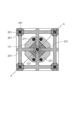


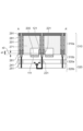


Classifications
-
- G—PHYSICS
- G01—MEASURING; TESTING
- G01S—RADIO DIRECTION-FINDING; RADIO NAVIGATION; DETERMINING DISTANCE OR VELOCITY BY USE OF RADIO WAVES; LOCATING OR PRESENCE-DETECTING BY USE OF THE REFLECTION OR RERADIATION OF RADIO WAVES; ANALOGOUS ARRANGEMENTS USING OTHER WAVES
- G01S17/00—Systems using the reflection or reradiation of electromagnetic waves other than radio waves, e.g. lidar systems
- G01S17/88—Lidar systems specially adapted for specific applications
- G01S17/89—Lidar systems specially adapted for specific applications for mapping or imaging
-
- H—ELECTRICITY
- H04—ELECTRIC COMMUNICATION TECHNIQUE
- H04N—PICTORIAL COMMUNICATION, e.g. TELEVISION
- H04N25/00—Circuitry of solid-state image sensors [SSIS]; Control thereof
- H04N25/70—SSIS architectures; Circuits associated therewith
- H04N25/76—Addressed sensors, e.g. MOS or CMOS sensors
- H04N25/766—Addressed sensors, e.g. MOS or CMOS sensors comprising control or output lines used for a plurality of functions, e.g. for pixel output, driving, reset or power
-
- H—ELECTRICITY
- H04—ELECTRIC COMMUNICATION TECHNIQUE
- H04N—PICTORIAL COMMUNICATION, e.g. TELEVISION
- H04N25/00—Circuitry of solid-state image sensors [SSIS]; Control thereof
- H04N25/70—SSIS architectures; Circuits associated therewith
- H04N25/79—Arrangements of circuitry being divided between different or multiple substrates, chips or circuit boards, e.g. stacked image sensors
-
- H—ELECTRICITY
- H10—SEMICONDUCTOR DEVICES; ELECTRIC SOLID-STATE DEVICES NOT OTHERWISE PROVIDED FOR
- H10F—INORGANIC SEMICONDUCTOR DEVICES SENSITIVE TO INFRARED RADIATION, LIGHT, ELECTROMAGNETIC RADIATION OF SHORTER WAVELENGTH OR CORPUSCULAR RADIATION
- H10F39/00—Integrated devices, or assemblies of multiple devices, comprising at least one element covered by group H10F30/00, e.g. radiation detectors comprising photodiode arrays
- H10F39/80—Constructional details of image sensors
- H10F39/803—Pixels having integrated switching, control, storage or amplification elements
- H10F39/8037—Pixels having integrated switching, control, storage or amplification elements the integrated elements comprising a transistor
- H10F39/80373—Pixels having integrated switching, control, storage or amplification elements the integrated elements comprising a transistor characterised by the gate of the transistor
-
- H—ELECTRICITY
- H10—SEMICONDUCTOR DEVICES; ELECTRIC SOLID-STATE DEVICES NOT OTHERWISE PROVIDED FOR
- H10F—INORGANIC SEMICONDUCTOR DEVICES SENSITIVE TO INFRARED RADIATION, LIGHT, ELECTROMAGNETIC RADIATION OF SHORTER WAVELENGTH OR CORPUSCULAR RADIATION
- H10F39/00—Integrated devices, or assemblies of multiple devices, comprising at least one element covered by group H10F30/00, e.g. radiation detectors comprising photodiode arrays
- H10F39/80—Constructional details of image sensors
- H10F39/809—Constructional details of image sensors of hybrid image sensors
-
- H—ELECTRICITY
- H10—SEMICONDUCTOR DEVICES; ELECTRIC SOLID-STATE DEVICES NOT OTHERWISE PROVIDED FOR
- H10F—INORGANIC SEMICONDUCTOR DEVICES SENSITIVE TO INFRARED RADIATION, LIGHT, ELECTROMAGNETIC RADIATION OF SHORTER WAVELENGTH OR CORPUSCULAR RADIATION
- H10F39/00—Integrated devices, or assemblies of multiple devices, comprising at least one element covered by group H10F30/00, e.g. radiation detectors comprising photodiode arrays
- H10F39/80—Constructional details of image sensors
- H10F39/811—Interconnections
-
- H—ELECTRICITY
- H04—ELECTRIC COMMUNICATION TECHNIQUE
- H04N—PICTORIAL COMMUNICATION, e.g. TELEVISION
- H04N25/00—Circuitry of solid-state image sensors [SSIS]; Control thereof
- H04N25/70—SSIS architectures; Circuits associated therewith
- H04N25/76—Addressed sensors, e.g. MOS or CMOS sensors
- H04N25/77—Pixel circuitry, e.g. memories, A/D converters, pixel amplifiers, shared circuits or shared components
- H04N25/778—Pixel circuitry, e.g. memories, A/D converters, pixel amplifiers, shared circuits or shared components comprising amplifiers shared between a plurality of pixels, i.e. at least one part of the amplifier must be on the sensor array itself
Landscapes
- Engineering & Computer Science (AREA)
- Physics & Mathematics (AREA)
- Multimedia (AREA)
- Signal Processing (AREA)
- Computer Networks & Wireless Communication (AREA)
- Electromagnetism (AREA)
- General Physics & Mathematics (AREA)
- Radar, Positioning & Navigation (AREA)
- Remote Sensing (AREA)
- Solid State Image Pick-Up Elements (AREA)
- Apparatus For Radiation Diagnosis (AREA)
- Inverter Devices (AREA)
Priority Applications (3)
| Application Number | Priority Date | Filing Date | Title |
|---|---|---|---|
| JP2023083369A JP2024166932A (ja) | 2023-05-19 | 2023-05-19 | 光電変換装置、光電変換システム |
| TW113117691A TW202515386A (zh) | 2023-05-19 | 2024-05-14 | 轉換裝置、轉換系統、及行動體 |
| US18/665,314 US20240387575A1 (en) | 2023-05-19 | 2024-05-15 | Conversion device, conversion system, and moving body |
Applications Claiming Priority (1)
| Application Number | Priority Date | Filing Date | Title |
|---|---|---|---|
| JP2023083369A JP2024166932A (ja) | 2023-05-19 | 2023-05-19 | 光電変換装置、光電変換システム |
Publications (2)
| Publication Number | Publication Date |
|---|---|
| JP2024166932A true JP2024166932A (ja) | 2024-11-29 |
| JP2024166932A5 JP2024166932A5 (cg-RX-API-DMAC7.html) | 2026-05-15 |
Family
ID=93463622
Family Applications (1)
| Application Number | Title | Priority Date | Filing Date |
|---|---|---|---|
| JP2023083369A Pending JP2024166932A (ja) | 2023-05-19 | 2023-05-19 | 光電変換装置、光電変換システム |
Country Status (3)
| Country | Link |
|---|---|
| US (1) | US20240387575A1 (cg-RX-API-DMAC7.html) |
| JP (1) | JP2024166932A (cg-RX-API-DMAC7.html) |
| TW (1) | TW202515386A (cg-RX-API-DMAC7.html) |
-
2023
- 2023-05-19 JP JP2023083369A patent/JP2024166932A/ja active Pending
-
2024
- 2024-05-14 TW TW113117691A patent/TW202515386A/zh unknown
- 2024-05-15 US US18/665,314 patent/US20240387575A1/en active Pending
Also Published As
| Publication number | Publication date |
|---|---|
| US20240387575A1 (en) | 2024-11-21 |
| TW202515386A (zh) | 2025-04-01 |
Similar Documents
| Publication | Publication Date | Title |
|---|---|---|
| JP7551589B2 (ja) | 光電変換装置、光電変換システム | |
| JP7635034B2 (ja) | 光電変換装置、光電変換システム、および移動体 | |
| US12543393B2 (en) | Photoelectric conversion apparatus and photoelectric conversion system having a concentration of impurity of a conductivity type in one region higher than another region | |
| US20250228020A1 (en) | Photodetector and electronic apparatus | |
| JP7799548B2 (ja) | 光電変換素子及び光電変換装置 | |
| WO2024004516A1 (ja) | 光電変換装置、光電変換システム | |
| US20250176302A1 (en) | Apparatus, system, and movable body | |
| US20250119663A1 (en) | Photoelectric conversion apparatus, photoelectric conversion system, and moving object | |
| US10777611B1 (en) | Image sensor | |
| US12477855B2 (en) | Photoelectric conversion device having signal readout circuits and photoelectric conversion system | |
| JP7532451B2 (ja) | 光電変換装置 | |
| JP7817835B2 (ja) | 光電変換装置および光電変換システム | |
| JP2025088184A (ja) | 光電変換装置 | |
| JP2024078413A (ja) | 半導体デバイスの製法 | |
| JP2024153346A (ja) | 光電変換装置、該光電変換装置を用いるシステム及び移動体 | |
| JP2024078501A (ja) | 光電変換装置、機器 | |
| US20240387575A1 (en) | Conversion device, conversion system, and moving body | |
| US20240145502A1 (en) | Photoelectric conversion device having insulator with a band shape, and photoelectric conversion system | |
| US12588310B2 (en) | Photoelectric conversion apparatus, photoelectric conversion system, and moving body | |
| US20230395637A1 (en) | Photoelectric conversion apparatus and photoelectric conversion system | |
| US20250040283A1 (en) | Light detection device and electronic device | |
| US20240339477A1 (en) | Semiconductor device, photoelectric conversion system, movable object | |
| US20240347573A1 (en) | Apparatus | |
| JP2025064694A (ja) | 光電変換装置、移動体および機器 | |
| JP2024164697A (ja) | 光電変換装置および機器 |
Legal Events
| Date | Code | Title | Description |
|---|---|---|---|
| RD01 | Notification of change of attorney |
Free format text: JAPANESE INTERMEDIATE CODE: A7421 Effective date: 20231213 |
|
| A521 | Request for written amendment filed |
Free format text: JAPANESE INTERMEDIATE CODE: A523 Effective date: 20260507 |
|
| A621 | Written request for application examination |
Free format text: JAPANESE INTERMEDIATE CODE: A621 Effective date: 20260507 |