JP2024166364A - Filter Device - Google Patents
Filter Device Download PDFInfo
- Publication number
- JP2024166364A JP2024166364A JP2024161131A JP2024161131A JP2024166364A JP 2024166364 A JP2024166364 A JP 2024166364A JP 2024161131 A JP2024161131 A JP 2024161131A JP 2024161131 A JP2024161131 A JP 2024161131A JP 2024166364 A JP2024166364 A JP 2024166364A
- Authority
- JP
- Japan
- Prior art keywords
- electrode
- resonator
- idt electrode
- electrode fingers
- inductor
- Prior art date
- Legal status (The legal status is an assumption and is not a legal conclusion. Google has not performed a legal analysis and makes no representation as to the accuracy of the status listed.)
- Granted
Links
Images






Classifications
-
- H—ELECTRICITY
- H03—ELECTRONIC CIRCUITRY
- H03H—IMPEDANCE NETWORKS, e.g. RESONANT CIRCUITS; RESONATORS
- H03H9/00—Networks comprising electromechanical or electro-acoustic elements; Electromechanical resonators
- H03H9/15—Constructional features of resonators consisting of piezoelectric or electrostrictive material
- H03H9/205—Constructional features of resonators consisting of piezoelectric or electrostrictive material having multiple resonators
-
- H—ELECTRICITY
- H03—ELECTRONIC CIRCUITRY
- H03H—IMPEDANCE NETWORKS, e.g. RESONANT CIRCUITS; RESONATORS
- H03H9/00—Networks comprising electromechanical or electro-acoustic elements; Electromechanical resonators
- H03H9/46—Filters
- H03H9/54—Filters comprising resonators of piezoelectric or electrostrictive material
- H03H9/542—Filters comprising resonators of piezoelectric or electrostrictive material including passive elements
-
- H—ELECTRICITY
- H03—ELECTRONIC CIRCUITRY
- H03H—IMPEDANCE NETWORKS, e.g. RESONANT CIRCUITS; RESONATORS
- H03H9/00—Networks comprising electromechanical or electro-acoustic elements; Electromechanical resonators
- H03H9/02—Details
- H03H9/02007—Details of bulk acoustic wave devices
- H03H9/02015—Characteristics of piezoelectric layers, e.g. cutting angles
-
- H—ELECTRICITY
- H03—ELECTRONIC CIRCUITRY
- H03H—IMPEDANCE NETWORKS, e.g. RESONANT CIRCUITS; RESONATORS
- H03H9/00—Networks comprising electromechanical or electro-acoustic elements; Electromechanical resonators
- H03H9/02—Details
- H03H9/02535—Details of surface acoustic wave devices
- H03H9/02543—Characteristics of substrate, e.g. cutting angles
- H03H9/02574—Characteristics of substrate, e.g. cutting angles of combined substrates, multilayered substrates, piezoelectrical layers on not-piezoelectrical substrate
-
- H—ELECTRICITY
- H03—ELECTRONIC CIRCUITRY
- H03H—IMPEDANCE NETWORKS, e.g. RESONANT CIRCUITS; RESONATORS
- H03H9/00—Networks comprising electromechanical or electro-acoustic elements; Electromechanical resonators
- H03H9/02—Details
- H03H9/02535—Details of surface acoustic wave devices
- H03H9/02818—Means for compensation or elimination of undesirable effects
- H03H9/02858—Means for compensation or elimination of undesirable effects of wave front distortion
-
- H—ELECTRICITY
- H03—ELECTRONIC CIRCUITRY
- H03H—IMPEDANCE NETWORKS, e.g. RESONANT CIRCUITS; RESONATORS
- H03H9/00—Networks comprising electromechanical or electro-acoustic elements; Electromechanical resonators
- H03H9/02—Details
- H03H9/02535—Details of surface acoustic wave devices
- H03H9/02818—Means for compensation or elimination of undesirable effects
- H03H9/02881—Means for compensation or elimination of undesirable effects of diffraction of wave beam
-
- H—ELECTRICITY
- H03—ELECTRONIC CIRCUITRY
- H03H—IMPEDANCE NETWORKS, e.g. RESONANT CIRCUITS; RESONATORS
- H03H9/00—Networks comprising electromechanical or electro-acoustic elements; Electromechanical resonators
- H03H9/02—Details
- H03H9/05—Holders or supports
- H03H9/0538—Constructional combinations of supports or holders with electromechanical or other electronic elements
- H03H9/0547—Constructional combinations of supports or holders with electromechanical or other electronic elements consisting of a vertical arrangement
-
- H—ELECTRICITY
- H03—ELECTRONIC CIRCUITRY
- H03H—IMPEDANCE NETWORKS, e.g. RESONANT CIRCUITS; RESONATORS
- H03H9/00—Networks comprising electromechanical or electro-acoustic elements; Electromechanical resonators
- H03H9/02—Details
- H03H9/05—Holders or supports
- H03H9/10—Mounting in enclosures
- H03H9/1064—Mounting in enclosures for surface acoustic wave [SAW] devices
- H03H9/1071—Mounting in enclosures for surface acoustic wave [SAW] devices the enclosure being defined by a frame built on a substrate and a cap, the frame having no mechanical contact with the SAW device
-
- H—ELECTRICITY
- H03—ELECTRONIC CIRCUITRY
- H03H—IMPEDANCE NETWORKS, e.g. RESONANT CIRCUITS; RESONATORS
- H03H9/00—Networks comprising electromechanical or electro-acoustic elements; Electromechanical resonators
- H03H9/02—Details
- H03H9/125—Driving means, e.g. electrodes, coils
- H03H9/145—Driving means, e.g. electrodes, coils for networks using surface acoustic waves
- H03H9/14517—Means for weighting
- H03H9/14526—Finger withdrawal
-
- H—ELECTRICITY
- H03—ELECTRONIC CIRCUITRY
- H03H—IMPEDANCE NETWORKS, e.g. RESONANT CIRCUITS; RESONATORS
- H03H9/00—Networks comprising electromechanical or electro-acoustic elements; Electromechanical resonators
- H03H9/02—Details
- H03H9/125—Driving means, e.g. electrodes, coils
- H03H9/145—Driving means, e.g. electrodes, coils for networks using surface acoustic waves
- H03H9/14538—Formation
- H03H9/14541—Multilayer finger or busbar electrode
-
- H—ELECTRICITY
- H03—ELECTRONIC CIRCUITRY
- H03H—IMPEDANCE NETWORKS, e.g. RESONANT CIRCUITS; RESONATORS
- H03H9/00—Networks comprising electromechanical or electro-acoustic elements; Electromechanical resonators
- H03H9/02—Details
- H03H9/125—Driving means, e.g. electrodes, coils
- H03H9/145—Driving means, e.g. electrodes, coils for networks using surface acoustic waves
- H03H9/14544—Transducers of particular shape or position
- H03H9/14547—Fan shaped; Tilted; Shifted; Slanted; Tapered; Arched; Stepped finger transducers
-
- H—ELECTRICITY
- H03—ELECTRONIC CIRCUITRY
- H03H—IMPEDANCE NETWORKS, e.g. RESONANT CIRCUITS; RESONATORS
- H03H9/00—Networks comprising electromechanical or electro-acoustic elements; Electromechanical resonators
- H03H9/02—Details
- H03H9/125—Driving means, e.g. electrodes, coils
- H03H9/145—Driving means, e.g. electrodes, coils for networks using surface acoustic waves
- H03H9/14544—Transducers of particular shape or position
- H03H9/14558—Slanted, tapered or fan shaped transducers
-
- H—ELECTRICITY
- H03—ELECTRONIC CIRCUITRY
- H03H—IMPEDANCE NETWORKS, e.g. RESONANT CIRCUITS; RESONATORS
- H03H9/00—Networks comprising electromechanical or electro-acoustic elements; Electromechanical resonators
- H03H9/02—Details
- H03H9/125—Driving means, e.g. electrodes, coils
- H03H9/145—Driving means, e.g. electrodes, coils for networks using surface acoustic waves
- H03H9/14544—Transducers of particular shape or position
- H03H9/1457—Transducers having different finger widths
-
- H—ELECTRICITY
- H03—ELECTRONIC CIRCUITRY
- H03H—IMPEDANCE NETWORKS, e.g. RESONANT CIRCUITS; RESONATORS
- H03H9/00—Networks comprising electromechanical or electro-acoustic elements; Electromechanical resonators
- H03H9/02—Details
- H03H9/125—Driving means, e.g. electrodes, coils
- H03H9/145—Driving means, e.g. electrodes, coils for networks using surface acoustic waves
- H03H9/14544—Transducers of particular shape or position
- H03H9/14573—Arrow type transducers
-
- H—ELECTRICITY
- H03—ELECTRONIC CIRCUITRY
- H03H—IMPEDANCE NETWORKS, e.g. RESONANT CIRCUITS; RESONATORS
- H03H9/00—Networks comprising electromechanical or electro-acoustic elements; Electromechanical resonators
- H03H9/15—Constructional features of resonators consisting of piezoelectric or electrostrictive material
- H03H9/17—Constructional features of resonators consisting of piezoelectric or electrostrictive material having a single resonator
-
- H—ELECTRICITY
- H03—ELECTRONIC CIRCUITRY
- H03H—IMPEDANCE NETWORKS, e.g. RESONANT CIRCUITS; RESONATORS
- H03H9/00—Networks comprising electromechanical or electro-acoustic elements; Electromechanical resonators
- H03H9/46—Filters
- H03H9/54—Filters comprising resonators of piezoelectric or electrostrictive material
-
- H—ELECTRICITY
- H03—ELECTRONIC CIRCUITRY
- H03H—IMPEDANCE NETWORKS, e.g. RESONANT CIRCUITS; RESONATORS
- H03H9/00—Networks comprising electromechanical or electro-acoustic elements; Electromechanical resonators
- H03H9/46—Filters
- H03H9/54—Filters comprising resonators of piezoelectric or electrostrictive material
- H03H9/58—Multiple crystal filters
- H03H9/60—Electric coupling means therefor
- H03H9/605—Electric coupling means therefor consisting of a ladder configuration
-
- H—ELECTRICITY
- H03—ELECTRONIC CIRCUITRY
- H03H—IMPEDANCE NETWORKS, e.g. RESONANT CIRCUITS; RESONATORS
- H03H9/00—Networks comprising electromechanical or electro-acoustic elements; Electromechanical resonators
- H03H9/46—Filters
- H03H9/64—Filters using surface acoustic waves
- H03H9/6423—Means for obtaining a particular transfer characteristic
- H03H9/6433—Coupled resonator filters
- H03H9/6483—Ladder SAW filters
Landscapes
- Physics & Mathematics (AREA)
- Acoustics & Sound (AREA)
- Chemical & Material Sciences (AREA)
- Crystallography & Structural Chemistry (AREA)
- Surface Acoustic Wave Elements And Circuit Networks Thereof (AREA)
- Piezo-Electric Or Mechanical Vibrators, Or Delay Or Filter Circuits (AREA)
Abstract
【課題】通過帯域を広くすることができ、しかも小型化を進めることができる、フィルタ装置を提供する。【解決手段】本発明のフィルタ装置1は、複数の直列腕共振子及び少なくとも1つの並列腕共振子を含む複数の共振子を備える。複数の共振子が、複数の共振子のうち最も比帯域の値が大きい第1の共振子としての直列腕共振子S23と、第1の共振子以外の少なくとも1つの第2の共振子とを含む。複数の直列腕共振子が第1の共振子(直列腕共振子S23)及び第2の共振子を含む。フィルタ装置1は、第1の共振子(直列腕共振子S23)に直列に接続されているインダクタである第1のインダクタ(インダクタL)をさらに備える。第2の共振子である直列腕共振子が、インダクタに接続されていない直列腕共振子を含む。【選択図】図10[Problem] To provide a filter device that can widen the passband and also facilitate miniaturization. [Solution] A filter device 1 of the present invention includes a plurality of resonators including a plurality of series arm resonators and at least one parallel arm resonator. The plurality of resonators includes a series arm resonator S23 as a first resonator having the largest band ratio value among the plurality of resonators, and at least one second resonator other than the first resonator. The plurality of series arm resonators include a first resonator (series arm resonator S23) and a second resonator. The filter device 1 further includes a first inductor (inductor L) that is an inductor connected in series to the first resonator (series arm resonator S23). The series arm resonator that is the second resonator includes a series arm resonator that is not connected to the inductor. [Selected Figure] Figure 10
Description
本発明は、ラダー型回路を含むフィルタ装置に関する。 The present invention relates to a filter device including a ladder circuit.
従来、弾性波装置が携帯電話機のフィルタなどに広く用いられている。下記の特許文献1には、直列腕共振子及び並列腕共振子に弾性波装置が用いられたラダー型フィルタの一例が記載されている。このラダー型フィルタにおいては、2つの端子の間に、5つの直列腕共振子が互いに直列に接続されている。両端の直列腕共振子と、双方の端子との間に、それぞれインダクタが接続されている。両端の直列腕共振子の各共振周波数と、上記両端の直列腕共振子以外の3つの直列腕共振子の共振周波数とが異ならされている。これにより、ラダー型フィルタの通過帯域の拡大、及び通過帯域外における減衰量を大きくすることが図られている。
Conventionally, acoustic wave devices have been widely used in filters for mobile phones and the like. The following
ラダー型フィルタでは、比帯域の値が小さい弾性波共振子は、通過帯域の端部における急峻性を高めるために用いられることがあった。他方、比帯域の値が大きい弾性波共振子は、通過帯域の拡大のために用いられることがあった。高い急峻性及び広い通過帯域を実現するためには、比帯域の値が小さい弾性波共振子、及び比帯域の値が大きい弾性波共振子の双方を要する。 In ladder-type filters, elastic wave resonators with small bandwidth ratios are sometimes used to increase the steepness at the ends of the passband. On the other hand, elastic wave resonators with large bandwidth ratios are sometimes used to expand the passband. In order to achieve high steepness and a wide passband, both elastic wave resonators with small bandwidth ratios and elastic wave resonators with large bandwidth ratios are required.
ここで、弾性波共振子の比帯域の値を大きくするために、弾性波共振子にインダクタが接続されることがある。インダクタのインダクタンスを高くすることにより、比帯域の値を大きくし得る。しかしながら、インダクタのインダクタンスを高くすると、インダクタが大型になり、フィルタ装置全体としても大型になりがちであった。 Here, in order to increase the relative bandwidth of the elastic wave resonator, an inductor may be connected to the elastic wave resonator. The relative bandwidth can be increased by increasing the inductance of the inductor. However, increasing the inductance of the inductor increases the size of the inductor, which tends to increase the size of the entire filter device.
本発明の目的は、通過帯域を広くすることができ、しかも小型化を進めることができる、フィルタ装置を提供することにある。 The object of the present invention is to provide a filter device that can widen the passband and can be made smaller.
本発明に係るフィルタ装置は、少なくとも1つの直列腕共振子及び少なくとも1つの並列腕共振子を含む複数の共振子を備え、前記複数の共振子が、前記複数の共振子のうち最も比帯域の値が大きい第1の共振子と、前記第1の共振子以外の少なくとも1つの第2の共振子とを含み、前記第1の共振子に直列に接続されているインダクタをさらに備える。 The filter device according to the present invention includes a plurality of resonators including at least one series arm resonator and at least one parallel arm resonator, the plurality of resonators including a first resonator having the largest band ratio value among the plurality of resonators and at least one second resonator other than the first resonator, and further includes an inductor connected in series to the first resonator.
本発明に係るフィルタ装置によれば、通過帯域を広くすることができ、しかも小型化を進めることができる。 The filter device of the present invention can widen the passband and also facilitate miniaturization.
以下、図面を参照しつつ、本発明の具体的な実施形態を説明することにより、本発明を明らかにする。 The present invention will be clarified below by explaining specific embodiments of the present invention with reference to the drawings.
なお、本明細書に記載の各実施形態は、例示的なものであり、異なる実施形態間において、構成の部分的な置換または組み合わせが可能であることを指摘しておく。 It should be noted that each embodiment described in this specification is illustrative, and partial substitution or combination of configurations is possible between different embodiments.
図1は、本発明の第1の実施形態に係るフィルタ装置の回路図である。 Figure 1 is a circuit diagram of a filter device according to a first embodiment of the present invention.
フィルタ装置1は、第1の信号端子9A及び第2の信号端子9Bと、複数の共振子とを有する。具体的には、複数の共振子は、複数の直列腕共振子と、複数の並列腕共振子とを含む。複数の直列腕共振子は、直列腕共振子S1、直列腕共振子S2、直列腕共振子S3、直列腕共振子S4及び直列腕共振子S5である。複数の並列腕共振子は、並列腕共振子P1、並列腕共振子P2、並列腕共振子P3及び並列腕共振子P4である。本実施形態においては、複数の共振子はいずれも弾性波共振子である。具体的には、複数の共振子は弾性表面波共振子である。もっとも、複数の共振子はバルク波共振子もあってもよい。
The
本実施形態においては、第1の信号端子9Aはアンテナ端子である。すなわち、第1の信号端子9Aはアンテナに接続される。第1の信号端子9A及び第2の信号端子9Bは、電極パッドとして設けられていてもよく、あるいは配線として設けられていてもよい。
In this embodiment, the
直列腕共振子S1、直列腕共振子S2、直列腕共振子S3、直列腕共振子S4及び直列腕共振子S5は、第1の信号端子9Aと第2の信号端子9Bとの間に互いに直列に接続されている。直列腕共振子S1及び直列腕共振子S2の間の接続点とグラウンド電位との間に、並列腕共振子P1が接続されている。直列腕共振子S2及び直列腕共振子S3の間の接続点とグラウンド電位との間に、並列腕共振子P2が接続されている。直列腕共振子S3及び直列腕共振子S4の間の接続点とグラウンド電位との間に、並列腕共振子P3が接続されている。直列腕共振子S4及び直列腕共振子S5の間の接続点とグラウンド電位との間に、並列腕共振子P4が接続されている。なお、フィルタ装置1の複数の共振子は、少なくとも1つの直列腕共振子と、少なくとも1つの並列腕共振子とを含んでいればよい。フィルタ装置1はラダー型回路を含んでいればよい。フィルタ装置1は、例えば、縦結合共振子型弾性波フィルタを含んでいてもよい。
The series arm resonators S1, S2, S3, S4, and S5 are connected in series between the
ここで、複数の共振子は、第1の共振子と、複数の第2の共振子とを含む。第1の共振子の比帯域の値は、複数の共振子の比帯域の値のうち最も大きい。第2の共振子は、第1の共振子以外の全ての共振子である。本実施形態では、第1の共振子は並列腕共振子P4である。第2の共振子は、直列腕共振子S1、直列腕共振子S2、直列腕共振子S3、直列腕共振子S4及び直列腕共振子S5、並びに並列腕共振P1、並列腕共振子P2及び並列腕共振子P3である。なお、本明細書において比帯域は、個々の共振子の比帯域をいう。すなわち、比帯域をΔf、共振周波数をfr、反共振周波数をfaとしたときに、Δf=(|fa-fr|/fr)×100[%]である。第1の共振子の比帯域は5%である。他方、各第2の共振子の比帯域はそれぞれ3%である。もっとも、第1の共振子及び第2の共振子の比帯域は上記に限定されない。 Here, the multiple resonators include a first resonator and multiple second resonators. The value of the fractional bandwidth of the first resonator is the largest among the values of the fractional bandwidth of the multiple resonators. The second resonator is all resonators other than the first resonator. In this embodiment, the first resonator is the parallel arm resonator P4. The second resonators are the series arm resonator S1, the series arm resonator S2, the series arm resonator S3, the series arm resonator S4, and the series arm resonator S5, as well as the parallel arm resonator P1, the parallel arm resonator P2, and the parallel arm resonator P3. In this specification, the fractional bandwidth refers to the fractional bandwidth of each resonator. That is, when the fractional bandwidth is Δf, the resonant frequency is fr, and the anti-resonant frequency is fa, Δf = (|fa-fr|/fr) x 100 [%]. The fractional bandwidth of the first resonator is 5%. On the other hand, the fractional bandwidth of each second resonator is 3%. However, the relative bandwidths of the first and second resonators are not limited to the above.
フィルタ装置1は、第1のインダクタ及び第2のインダクタを有する。第1のインダクタは、第1の共振子に直列に接続されているインダクタである。第2のインダクタは、第2の共振子に接続されているインダクタである。具体的には、第1のインダクタはインダクタLである。第2のインダクタはインダクタMである。インダクタLは、第1の共振子である並列腕共振子P4と、グラウンド電位との間に接続されている。なお、インダクタLは、並列腕共振子P4に、他の共振子を介さず接続されている。インダクタMは、並列腕共振子P2とグラウンド電位との間に接続されている。
The
インダクタLは、並列腕共振子P4の比帯域の値を大きくするためのインダクタである。これにより、フィルタ装置1の通過帯域を広くすることができる。他方、インダクタMは、インピーダンスマッチング用のインダクタである。
Inductor L is an inductor for increasing the band ratio of parallel arm resonator P4. This allows the passband of
本実施形態の特徴は、第1の共振子としての並列腕共振子P4に、第1のインダクタとしてのインダクタLが直列に接続されていることにある。上記のように、第1の共振子の比帯域の値は、複数の共振子の比帯域の値のうち最も大きい。そのため、第1の共振子の比帯域の値を大きくするために要する、第1のインダクタのインダクタンスを小さくすることができる。それによって、第1のインダクタを小型にすることができる。従って、フィルタ装置1の通過帯域を広くすることができ、しかも小型化を効果的に進めることができる。この詳細を以下において説明する。
The feature of this embodiment is that the inductor L as the first inductor is connected in series to the parallel arm resonator P4 as the first resonator. As described above, the band ratio value of the first resonator is the largest among the band ratio values of the multiple resonators. Therefore, the inductance of the first inductor required to increase the band ratio value of the first resonator can be reduced. This allows the first inductor to be made smaller. Therefore, the pass band of the
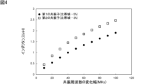
弾性波共振子にインダクタを接続すると、共振周波数が低くなる一方で、反共振周波数は変化しない。それによって、比帯域の値が大きくなる。ここで、第1の共振子及び第2の共振子のそれぞれにインダクタを接続した場合において、共振周波数を50MHz低くするために必要なインダクタのインダクタンスを比較した。該比較においては、第1の実施形態と同様に、第1の共振子の比帯域を5%とし、第2の共振子の比帯域を3%とした。さらに、共振周波数を低くする幅を10MHz以上、100MHz以下の範囲において、10MHz刻みで変化させて、上記と同様の比較を行った。 When an inductor is connected to an elastic wave resonator, the resonant frequency is lowered while the anti-resonant frequency remains unchanged. This increases the value of the relative bandwidth. Here, the inductance of the inductor required to lower the resonant frequency by 50 MHz when an inductor is connected to each of the first and second resonators was compared. In this comparison, as in the first embodiment, the relative bandwidth of the first resonator was set to 5% and the relative bandwidth of the second resonator was set to 3%. Furthermore, the width by which the resonant frequency was lowered was changed in 10 MHz increments in the range of 10 MHz or more and 100 MHz or less, and a similar comparison was made as above.
図2は、第2の共振子にインダクタが接続されたことによる比帯域の変化を示す図である。図3は、第1の共振子にインダクタが接続されたことによる比帯域の変化を示す図である。図4は、共振子にインダクタが接続された場合における、インダクタのインダクタンスと、共振周波数の変化幅との関係を示す図である。 Figure 2 shows the change in the bandwidth ratio when an inductor is connected to the second resonator. Figure 3 shows the change in the bandwidth ratio when an inductor is connected to the first resonator. Figure 4 shows the relationship between the inductance of the inductor and the change in the resonant frequency when an inductor is connected to a resonator.
図2及び図3に示すように、第1の共振子及び第2の共振子のそれぞれにおいて、共振周波数が50MHz低くなっている。このとき、図2に示すように、第2の共振子に接続されたインダクタのインダクタンスは1.67nHである。他方、図3に示すように、第1の共振子に接続されたインダクタのインダクタンスは1.18nHである。さらに、図4に示すように、共振周波数の変化幅が50MHz以外の場合も、第1の共振子に接続されたインダクタのインダクタンスは、第2の共振子に接続されたインダクタのインダクタンスよりも小さい。このように、第1の共振子においては、比帯域の値を効率的に大きくすることができる。なお、表1に図4の結果を示す。 As shown in Figures 2 and 3, the resonant frequency is 50 MHz lower in each of the first and second resonators. At this time, as shown in Figure 2, the inductance of the inductor connected to the second resonator is 1.67 nH. On the other hand, as shown in Figure 3, the inductance of the inductor connected to the first resonator is 1.18 nH. Furthermore, as shown in Figure 4, even when the resonant frequency change width is other than 50 MHz, the inductance of the inductor connected to the first resonator is smaller than the inductance of the inductor connected to the second resonator. In this way, the value of the bandwidth ratio can be efficiently increased in the first resonator. The results of Figure 4 are shown in Table 1.

以上のように、第1の共振子において、比帯域の値を大きくするために要するインダクタのインダクタンスは、第2の共振子において、比帯域の値を大きくするために要するインダクタのインダクタンスよりも小さいことがわかる。よって、フィルタ装置の通過帯域を広くする場合において、第1の共振子に接続されるインダクタを小型にすることができる。 As described above, it can be seen that the inductance of the inductor required to increase the band ratio in the first resonator is smaller than the inductance of the inductor required to increase the band ratio in the second resonator. Therefore, when widening the passband of the filter device, the inductor connected to the first resonator can be made smaller.
なお、本実施形態においては、第2のインダクタとしてのインダクタMのインダクタンスは、第1のインダクタとしてのインダクタLのインダクタンスよりも小さい。よって、フィルタ装置1の小型化をより確実に進めることができる。
In this embodiment, the inductance of the inductor M serving as the second inductor is smaller than the inductance of the inductor L serving as the first inductor. This makes it possible to more reliably reduce the size of the
図1に示すように、インダクタLは、並列腕共振子P4とグラウンド電位との間に接続されていることが好ましい。それによって、インピーダンスマッチングを行い易くすることができる。もっとも、インダクタLは、直列腕共振子S4及び直列腕共振子S5の間の接続点と、並列腕共振子P4との間に接続されていてもよい。すなわち、第1のインダクタは、第1の共振子に接続されている第2の共振子同士の接続点と、第1の共振子との間に接続されていてもよい。 As shown in FIG. 1, the inductor L is preferably connected between the parallel arm resonator P4 and the ground potential. This makes it easier to perform impedance matching. However, the inductor L may also be connected between the parallel arm resonator P4 and the connection point between the series arm resonators S4 and S5. In other words, the first inductor may be connected between the first resonator and the connection point between the second resonators connected to the first resonator.
なお、フィルタ装置が複数の第1の共振子を有する場合には、いずれか1つの第1の共振子に直列に第1のインダクタが接続されていることが好ましい。 When the filter device has multiple first resonators, it is preferable that the first inductor is connected in series to any one of the first resonators.
以下において、本実施形態のフィルタ装置1の構成の詳細を示す。
The following provides details of the configuration of the
図5は、第1の実施形態における第1の共振子の平面図である。 Figure 5 is a plan view of the first resonator in the first embodiment.
第1の共振子としての並列腕共振子P4は、圧電性基板2を有する。圧電性基板2上には、IDT電極3が設けられている。IDT電極3に交流電圧を印加することにより、弾性表面波が励振される。圧電性基板2上における、IDT電極3の弾性波伝搬方向両側には、1対の反射器8A及び反射器8Bが設けられている。
The parallel arm resonator P4, which serves as a first resonator, has a
IDT電極3は、第1のバスバー16及び第2のバスバー17と、複数の第1の電極指18及び複数の第2の電極指19とを有する。第1のバスバー16及び第2のバスバー17は互いに対向している。複数の第1の電極指18の一端は、それぞれ第1のバスバー16に接続されている。複数の第2の電極指19の一端は、それぞれ第2のバスバー17に接続されている。複数の第1の電極指18及び複数の第2の電極指19は互いに間挿し合っている。IDT電極3、反射器8A及び反射器8Bは、単層の金属膜からなっていてもよく、積層金属膜からなっていてもよい。なお、以下においては、第1の電極指18及び第2の電極指19をまとめて電極指と記載することがある。
The
圧電性基板2上に、IDT電極3を覆うように誘電体膜が設けられていてもよい。これにより、IDT電極3が破損し難い。誘電体膜の材料としては、例えば、酸化ケイ素、窒化ケイ素または酸窒化ケイ素などを用いることができる。
A dielectric film may be provided on the
図6は、図5中のI-I線に沿う断面図である。 Figure 6 is a cross-sectional view taken along line I-I in Figure 5.
本実施形態の圧電性基板2は、高音速材料層としての高音速支持基板5と、低音速膜6と、圧電体層7とを有する。より具体的には、高音速支持基板5上に低音速膜6が設けられている。低音速膜6上に圧電体層7が設けられている。圧電体層7は主面7aを有する。圧電体層7の主面7aには、IDT電極3、反射器8A及び反射器8Bが設けられている。
The
圧電体層7の材料としては、例えば、タンタル酸リチウム、ニオブ酸リチウム、酸化亜鉛、窒化アルミニウム、水晶、またはPZT(チタン酸ジルコン酸鉛)などを用いることができる。
Materials that can be used for the
高音速材料層は相対的に高音速な層である。より具体的には、高音速材料層を伝搬するバルク波の音速は圧電体層7を伝搬する弾性波の音速よりも高い。本実施形態では、高音速材料層は高音速支持基板5である。高音速材料層の材料としては、例えば、シリコン、酸化アルミニウム、炭化ケイ素、窒化ケイ素、酸窒化ケイ素、サファイア、タンタル酸リチウム、ニオブ酸リチウム、水晶、アルミナ、ジルコニア、コージライト、ムライト、ステアタイト、フォルステライト、マグネシア、DLC(ダイヤモンドライクカーボン)膜またはダイヤモンドなど、上記材料を主成分とする媒質を用いることができる。
The high acoustic velocity material layer is a layer with a relatively high acoustic velocity. More specifically, the acoustic velocity of the bulk waves propagating through the high acoustic velocity material layer is higher than the acoustic velocity of the elastic waves propagating through the
低音速膜6は相対的に低音速な膜である。より具体的には、低音速膜6を伝搬するバルク波の音速は、圧電体層7を伝搬するバルク波の音速よりも低い。低音速膜6の材料としては、例えば、ガラス、酸化ケイ素、酸窒化ケイ素、酸化リチウム、五酸化タンタル、または、酸化ケイ素にフッ素、炭素やホウ素を加えた化合物を主成分とする材料を用いることができる。
The low
本実施形態においては、高音速材料層としての高音速支持基板5、低音速膜6及び圧電体層7がこの順序において積層されている。それによって、弾性波のエネルギーを圧電体層7側に効果的に閉じ込めることができる。もっとも、圧電性基板2の構成は上記に限定されない。
In this embodiment, a high acoustic
他の共振子も、並列腕共振子P4と同様に、IDT電極及び1対の反射器を有する。フィルタ装置1においては、全ての共振子は圧電性基板2を共有している。もっとも、少なくとも1つの共振子が、他の共振子とは異なる圧電性基板を有していてもよい。
The other resonators, like the parallel arm resonator P4, also have an IDT electrode and a pair of reflectors. In the
上述したように、並列腕共振子P4にインダクタLを接続することにより、フィルタ装置1の通過帯域を広くすることができる。これを、本実施形態及び比較例を比較することにより示す。比較例は、インダクタLを有しない点において第1の実施形態と異なる。フィルタ装置1における圧電性基板2及びIDT電極3の構成、並びにインダクタL及びインダクタMのインダクタンスは以下の通りとした。比較例における各パラメータも、インダクタL以外においては、以下の各パラメータと同様である。
As described above, by connecting the inductor L to the parallel arm resonator P4, the passband of the
高音速支持基板5;材料…Si、厚み…125μm
低音速膜6;材料…SiO2、厚み…670nm
圧電体層7;材料…LiTaO3、厚み…600nm
IDT電極3;積層構造…圧電体層7側からTi層/AlCu層、厚み…圧電体層7側から12nm/162nm
インダクタL;インダクタンス…3nH
インダクタM;インダクタンス…0.3nH
High sound velocity support substrate 5: Material: Si, thickness: 125 μm
Low acoustic velocity film 6: material: SiO 2 , thickness: 670 nm
Piezoelectric layer 7: Material: LiTaO 3 , thickness: 600 nm
IDT electrode 3: laminated structure: Ti layer/AlCu layer from the
Inductor L; inductance...3nH
Inductor M: Inductance...0.3nH
図7は、第1の実施形態及び比較例の減衰量周波数特性を示す図である。 Figure 7 shows the attenuation frequency characteristics of the first embodiment and the comparative example.
図7に示すように、比較例の通過帯域よりも第1の実施形態の通過帯域が広いことがわかる。図7中に示す帯域Wは、Band41の通過帯域を示す。具体的には、Band41の通過帯域は2496MHz~2690MHzである。比較例のフィルタ装置においては、2496MHz付近において挿入損失が大きい。これに対して、第1の実施形態においては、並列腕共振子P4にインダクタLが接続されている。これにより、フィルタ装置1の通過帯域が広くなっており、2496MHz~2690MHzにおいて挿入損失が小さい。よって、フィルタ装置1をBand41のような広い帯域にも適用することができる。しかも、上述したように、通過帯域を広くするためのインダクタLを小型にすることができ、フィルタ装置1の小型化を進めることができる。
As shown in FIG. 7, it can be seen that the passband of the first embodiment is wider than that of the comparative example. Band W shown in FIG. 7 indicates the passband of Band 41. Specifically, the passband of Band 41 is 2496 MHz to 2690 MHz. In the filter device of the comparative example, the insertion loss is large near 2496 MHz. In contrast, in the first embodiment, an inductor L is connected to the parallel arm resonator P4. This widens the passband of the
図8は、第1の実施形態に係るフィルタ装置の略図的正面断面図である。図8においては、共振子を構成する電極を、矩形に2本の対角線を加えた略図により示す。 Figure 8 is a schematic front cross-sectional view of a filter device according to the first embodiment. In Figure 8, the electrodes that make up the resonator are shown as a simplified diagram of a rectangle with two diagonal lines added.
フィルタ装置1は実装基板10を有する。フィルタ装置1の複数の共振子は実装基板10に配置されている。本実施形態では、第1の共振子である並列腕共振子P4を構成する電極と、実装基板10との間にインダクタLが設けられている。
The
圧電体層7の主面7aには、複数の共振子の複数のIDT電極が設けられている。さらに、主面7aには、複数の端子が設けられている。複数の端子は、複数のグラウンド端子9C並びに上記第1の信号端子9A及び上記第2の信号端子9Bを含む。
The
さらに、主面7aには支持部材11が設けられている。支持部材11は、複数の端子の少なくとも一部を覆うように設けられている。支持部材11は開口部11aを有する。開口部11aは、複数の共振子の複数のIDT電極を囲んでいる。圧電体層7と共に支持部材11を挟むように、カバー部材12が設けられている。カバー部材12は、支持部材11の開口部11aを覆っている。これにより、圧電性基板2、支持部材11及びカバー部材12により囲まれた中空空間が設けられている。複数のIDT電極は、該中空空間内に配置されている。
Furthermore, a
カバー部材12内には、第1のインダクタとしてのインダクタLが設けられている。インダクタLは配線により構成されている。より具体的には、インダクタLは、配線電極La及び配線電極Lbと、ビア電極Lcとを有する。配線電極Laと配線電極Lbとが、ビア電極Lcに接続されている。これにより、インダクタLが構成されている。上記第2のインダクタも、インダクタLと同様に構成されている。なお、各インダクタにおける配線の引き回しの形状は特に限定されない。各インダクタの配線電極及びビア電極の個数も特に限定されない。
Inductor L is provided as a first inductor within the
支持部材11を貫通するように、複数の第1の貫通電極が設けられている。複数の第1の貫通電極は、第1の貫通電極13A及び第1の貫通電極13Bを含む。第1の貫通電極13Aの一端はグラウンド端子9Cに接続されている。第1の貫通電極13Aの他端は配線電極Laに接続されている。カバー部材12には、複数の第1の接続端子14Aが設けられている。配線電極Lbが、第1の接続端子14Aに接続されている。このように、第1の貫通電極13AはインダクタLを介して第1の接続端子14Aに接続されている。
A plurality of first through electrodes are provided so as to penetrate the
他方、第1の貫通電極13Bは、カバー部材12を貫通している。第1の貫通電極13Bの一端はグラウンド端子9Cに接続されている。第1の貫通電極13Bの他端は第1の接続端子14Aに接続されている。
On the other hand, the first through electrode 13B penetrates the
実装基板10の一方主面には、複数の第2の接続端子14Bが設けられている。実装基板10の他方主面には複数の第3の接続端子14Cが設けられている。さらに、実装基板10を貫通するように、複数の第2の貫通電極13Cが設けられている。第2の貫通電極13Cの一端は第2の接続端子14Bに接続されている。第2の貫通電極13Cの他端は第3の接続端子14Cに接続されている。
A plurality of
実装基板10の第2の接続端子14Bと、複数の共振子側の第1の接続端子14Aとを接続するように、バンプ15が設けられている。並列腕共振子P4は、グラウンド端子9C、第1の貫通電極13A、インダクタL、第1の接続端子14A、バンプ15、第2の接続端子14B、第2の貫通電極13C及び第3の接続端子14Cを介してグラウンド電位に接続される。複数の第2の共振子のうち、例えば並列腕共振子P3は、グラウンド端子9C、第1の貫通電極13B、第1の接続端子14A、バンプ15、第2の接続端子14B、第2の貫通電極13C及び第3の接続端子14Cを介してグラウンド電位に接続される。以上のように、フィルタ装置1の複数の共振子はWLP(Wafer Level Package)構造である。もっとも、複数の共振子はWLP構造には限定されない。
A
ところで、インダクタが配線により構成されている場合には、配線電極またはビア電極の長さが長いほど、インダクタンスが大きい。よって、要するインダクタンスが大きいほど、インダクタが大型になる。これに対して、本実施形態においては、インダクタLのインダクタンスが小さくとも、並列腕共振子P4の比帯域の値を大きくすることができる。よって、インダクタLが配線により構成されている場合には、本発明が好適である。 However, when an inductor is configured with wiring, the longer the length of the wiring electrode or via electrode, the larger the inductance. Therefore, the larger the required inductance, the larger the inductor. In contrast, in this embodiment, even if the inductance of the inductor L is small, the value of the bandwidth ratio of the parallel arm resonator P4 can be increased. Therefore, the present invention is suitable when the inductor L is configured with wiring.
インダクタLは、カバー部材12以外の部分に設けられていてもよい。例えば、図9に示す第1の変形例においては、インダクタLは実装基板10内に設けられている。インダクタLは、ビア電極23Aにより第2の接続端子14Bに接続されている。さらに、インダクタLは、ビア電極23Bにより第3の接続端子14Cに接続されている。なお、インダクタLは、カバー部材12内や実装基板10内に限られず、カバー部材12や実装基板10の表面に設けられていてもよい。あるいは、インダクタLは、圧電性基板2上に設けられていてもよい。
The inductor L may be provided in a portion other than the
第1の実施形態においては、第1の共振子は並列腕共振子である。もっとも、第1の共振子は直列腕共振子であってもよい。例えば、図10に示す第2の変形例おいては、複数の共振子のうち直列腕共振子S23の比帯域の値が最も大きい。すなわち、直列腕共振子S23が第1の共振子であり、並列腕共振子P24を含む他の共振子は、複数の第2の共振子である。直列腕共振子S2及び並列腕共振子P2の接続点と、直列腕共振子S23との間に第1のインダクタとしてのインダクタLが接続されている。インダクタLは、直列腕共振子S2に直列に接続されている。なお、インダクタLは、直列腕共振子S4及び並列腕共振子P3の接続点と、直列腕共振子S23との間に接続されていてもよい。本変形例においても、第1の実施形態と同様に、フィルタ装置の小型化を進めることができる。 In the first embodiment, the first resonator is a parallel arm resonator. However, the first resonator may be a series arm resonator. For example, in the second modification shown in FIG. 10, the series arm resonator S23 has the largest band ratio among the multiple resonators. That is, the series arm resonator S23 is the first resonator, and the other resonators including the parallel arm resonator P24 are multiple second resonators. An inductor L as a first inductor is connected between the connection point of the series arm resonator S2 and the parallel arm resonator P2 and the series arm resonator S23. The inductor L is connected in series to the series arm resonator S2. The inductor L may be connected between the connection point of the series arm resonator S4 and the parallel arm resonator P3 and the series arm resonator S23. In this modification, as in the first embodiment, the filter device can be made smaller.
もっとも、第1の共振子が並列腕共振子であり、第1のインダクタが該並列腕共振子に直列に接続されていることが好ましい。それによって、フィルタ装置の挿入損失の劣化が生じ難い。 However, it is preferable that the first resonator is a parallel arm resonator and the first inductor is connected in series to the parallel arm resonator. This makes it difficult for the insertion loss of the filter device to deteriorate.
図6に示すように、本実施形態の圧電性基板2においては、圧電体層7が、高音速材料層としての高音速支持基板5上に、低音速膜6を介して間接的に設けられている。もっとも、圧電性基板2の構成は上記に限定されない。以下において、圧電性基板の構成のみが第1の実施形態と異なる、第1の実施形態の第3の変形例及び第4の変形例を示す。第3の変形例及び第4の変形例においても、第1の実施形態と同様に、フィルタ装置の小型化を進めることができる。加えて、第1の実施形態と同様に、高音速材料層及び圧電体層を含む積層構造が設けられているため、弾性波のエネルギーを圧電体層側に効果的に閉じ込めることができる。
As shown in FIG. 6, in the
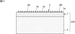
図11に示す第3の変形例においては、圧電性基板22Aは、高音速支持基板5と、圧電体層7とを有する。圧電体層7は、高音速材料層としての高音速支持基板5上に直接的に設けられている。
In the third modified example shown in FIG. 11, the
図12に示す第4の変形例においては、圧電性基板22Bは、支持基板24と、高音速材料層としての高音速膜25と、低音速膜6と、圧電体層7とを有する。より具体的には、支持基板24上に高音速膜25が設けられている。高音速膜25上に低音速膜6が設けられている。低音速膜6上に圧電体層7が設けられている。
In the fourth modified example shown in FIG. 12, the
支持基板24の材料としては、例えば、酸化アルミニウム、タンタル酸リチウム、ニオブ酸リチウム、水晶などの圧電体、アルミナ、サファイア、マグネシア、窒化ケイ素、窒化アルミニウム、炭化ケイ素、ジルコニア、コージライト、ムライト、ステアタイト、フォルステライトなどの各種セラミック、ダイヤモンド、ガラスなどの誘電体、シリコン、窒化ガリウムなどの半導体または樹脂などを用いることができる。
Materials that can be used for the
なお、圧電性基板は、支持基板24、高音速膜25及び圧電体層7の積層体であってもよい。あるいは、圧電性基板は、圧電体層のみからなる圧電基板であってもよい。
The piezoelectric substrate may be a laminate of a
第1の実施形態及びその変形例においては、圧電体層7は、IDT電極3が設けられている部分を含めて、他の層により支持されている。もっとも、圧電体層7は、平面視においてIDT電極3の少なくとも一部と重なる部分においては、他の層により支持されていなくともよい。より具体的には、圧電体層7以外の層の、平面視においてIDT電極3の少なくとも一部と重なる部分に、空洞部が設けられていてもよい。この場合、空洞部は圧電体層7側において開口していればよい。空洞部は、1層にのみ設けられていてもよく、複数の層にわたり設けられていてもよい。空洞部は凹部であってもよく、貫通孔であってもよい。このような空洞部が設けられている場合、共振子は板波を利用することが好ましい。
In the first embodiment and its modified example, the
ここで、第1の共振子のIDT電極を第1のIDT電極とし、第2の共振子のIDT電極を第2のIDT電極とする。以下においては、第1のIDT電極または第2のIDT電極の構成のみが第1の実施形態と異なる、第2~第5の実施形態を示す。第2~第5の実施形態においても、第1の実施形態と同様に、第1の共振子にインダクタLが接続されている。よって、フィルタ装置の通過帯域を広くすることができ、かつフィルタ装置の小型化を進めることができる。 Here, the IDT electrode of the first resonator is the first IDT electrode, and the IDT electrode of the second resonator is the second IDT electrode. In the following, second to fifth embodiments are shown, in which only the configuration of the first IDT electrode or the second IDT electrode differs from the first embodiment. In the second to fifth embodiments, as in the first embodiment, an inductor L is connected to the first resonator. Therefore, the passband of the filter device can be widened, and the filter device can be made more compact.
図13は、第2の実施形態における第1の共振子の平面図である。図14は、第2の実施形態における第2の共振子の平面図である。 Figure 13 is a plan view of a first resonator in the second embodiment. Figure 14 is a plan view of a second resonator in the second embodiment.
図13に示すように、本実施形態においては、第1の共振子の第1のIDT電極33Aの構成が第1の実施形態と異なる。第1の共振子は、ピストンモードを利用する弾性表面波共振子である。図14に示すように、本実施形態においては、第2の共振子の第2のIDT電極33Bの構成も第1の実施形態と異なる。第2のIDT電極33Bは傾斜型のIDT電極である。以下において、第1のIDT電極33A及び第2のIDT電極33Bの構成の詳細を説明する。
As shown in FIG. 13, in this embodiment, the configuration of the
図13に示すように、弾性波伝搬方向から見て、隣り合う第1の電極指18及び第2の電極指19が重なり合う領域は交叉領域Aである。交叉領域Aは、中央領域Cと、第1のエッジ領域E1及び第2のエッジ領域E2とを有する。ここで、複数の第1の電極指18及び複数の第2の電極指19が延びる方向を電極指延伸方向とする。なお、本実施形態においては、電極指延伸方向と弾性波伝搬方向とは直交する。中央領域Cは、交叉領域Aにおいて、電極指延伸方向における中央側に位置する領域である。一方で、第1のエッジ領域E1及び第2のエッジ領域E2は、中央領域Cを電極指延伸方向において挟むように配置されている。第1のエッジ領域E1は第1のバスバー16側に位置する。第2のエッジ領域E2は第2のバスバー17側に位置する。さらに、第1のIDT電極33Aは、第1のギャップ領域G1及び第2のギャップ領域G2を有する。第1のギャップ領域G1は、第1のエッジ領域E1と第1のバスバー16との間に位置する。第2のギャップ領域G2は、第2のエッジ領域E2と第2のバスバー17との間に位置する。
As shown in FIG. 13, the area where adjacent
第1のエッジ領域E1及び第2のエッジ領域E2における音速は、中央領域Cにおける音速よりも低い。他方、第1のギャップ領域G1及び第2のギャップ領域G2における音速は、中央領域Cにおける音速よりも高い。これにより、ピストンモードが成立し、横モードが抑制される。 The sound speed in the first edge region E1 and the second edge region E2 is lower than the sound speed in the central region C. On the other hand, the sound speed in the first gap region G1 and the second gap region G2 is higher than the sound speed in the central region C. This establishes the piston mode and suppresses the lateral mode.
より具体的には、本実施形態の第1のIDT電極33Aにおいては、第1のエッジ領域E1において、複数の第1の電極指18上及び複数の第2の電極指19上に質量付加膜35Aが設けられている。同様に、第2のエッジ領域E2においては、複数の第1の電極指18上及び第2の電極指19上に、質量付加膜35Bが設けられている。質量付加膜35A及び質量付加膜35Bは適宜の誘電体からなる。
More specifically, in the
質量付加膜35A及び質量付加膜35Bは帯状の形状を有する。これにより、質量付加膜35Aは、複数の第1の電極指18上及び複数の第2の電極指19上、並びに圧電性基板2上における電極指間に位置する部分にわたり設けられている。質量付加膜35Bも同様である。これにより、第1のエッジ領域E1及び第2のエッジ領域E2における音速が低くなっている。
The mass-adding
本実施形態においては、複数の電極指及び質量付加膜35Aが積層されている部分においては、圧電性基板2、複数の電極指及び質量付加膜35Aの順序において積層されている。なお、質量付加膜35Aは、圧電性基板2と、複数の第1の電極指18及び複数の第2の電極指19との間に設けられていてもよい。すなわち、複数の電極指及び質量付加膜35Aが積層されている部分において、圧電性基板2、質量付加膜35A及び複数の電極指の順序において積層されていてもよい。質量付加膜35Bも同様である。
In this embodiment, in the portion where the multiple electrode fingers and
なお、質量付加膜35A及び質量付加膜35Bは、複数の電極指上にわたり設けられていなくともよい。複数の質量付加膜35A及び複数の質量付加膜35Bが、各第1の電極指18及び各第2の電極指19と積層されていてもよい。この場合には、複数の質量付加膜35A及び複数の質量付加膜35Bは、金属からなっていてもよく、誘電体からなっていてもよい。質量付加膜35Aまたは質量付加膜35Bは、第1のエッジ領域E1及び第2のエッジ領域E2のうち少なくとも一方において、複数の第1の電極指18及び複数の第2の電極指19のうち少なくとも1本の電極指と積層されていればよい。もっとも、質量付加膜35A及び質量付加膜35Bが、第1のエッジ領域E1及び第2のエッジ領域E2の双方において、複数の電極指と積層されていることが好ましい。
The mass-adding
第1のギャップ領域G1においては、複数の第1の電極指18及び複数の第2の電極指19のうち複数の第1の電極指18のみが設けられている。よって、第1のギャップ領域G1における音速が高い。同様に、第2のギャップ領域G2においては、複数の第1の電極指18及び複数の第2の電極指19のうち複数の第2の電極指19のみが設けられている。よって、第2のギャップ領域G2における音速が高い。
In the first gap region G1, out of the multiple
中央領域Cにおける音速をV1、第1のエッジ領域E1及び第2のエッジ領域E2における音速をV2、第1のギャップ領域G1及び第2のギャップ領域G2における音速をV3としたときに、V2<V1<V3である。上記のような各音速の関係を図13に示す。なお、図13における音速の関係を示す部分においては、矢印Vで示すように、各音速の高さを示す線が左側に位置するほど音速が高いことを示す。 When the sound speed in the central region C is V1, the sound speed in the first edge region E1 and the second edge region E2 is V2, and the sound speed in the first gap region G1 and the second gap region G2 is V3, V2<V1<V3. The relationship between the above sound speeds is shown in FIG. 13. Note that in the portion showing the sound speed relationships in FIG. 13, as shown by the arrow V, the line indicating the height of each sound speed indicates a higher sound speed as it is positioned to the left.
本実施形態では、第1のIDT電極33Aが上記のような構成を有するため、第1の共振子において、容量に対する比帯域の比を大きくすることができる。そのため、第1の共振子を大型にせずして、比帯域の値をより一層大きくすることができる。そして、第1の共振子の比帯域の値をさらに大きくするための第1のインダクタのインダクタンスを、より一層小さくすることができる。従って、フィルタ装置の通過帯域を広くすることができ、かつフィルタ装置の小型化をより一層進めることができる。
In this embodiment, since the
他方、図14に示すように、第2のIDT電極33Bは傾斜型IDT電極である。より具体的には、複数の第1の電極指18の先端を結ぶことにより形成される仮想線を第1の包絡線B1としたときに、第1の包絡線B1は弾性波伝搬方向に対して傾斜している。同様に、複数の第2の電極指19の先端を結ぶことにより形成される仮想線を第2の包絡線B2としたときに、第2の包絡線B2は、弾性波伝搬方向に対して傾斜している。これにより、横モードに起因するスプリアスを抑制することができる。
On the other hand, as shown in FIG. 14, the
なお、第2のIDT電極33Bにおいては、第1のバスバー36及び第2のバスバー37は弾性波伝搬方向に対して傾斜して延びている。もっとも、これに限定されるものではない。
In the
図15は、第2の実施形態の変形例における第1のIDT電極の平面図である。 Figure 15 is a plan view of the first IDT electrode in a modified example of the second embodiment.
本変形例においても、第2の実施形態と同様に、第1の共振子はピストンモードを利用している。より具体的には、第1のIDT電極43Aの複数の第1の電極指48は、第1のエッジ領域E1に位置する幅広部48aを有する。さらに、複数の第1の電極指48は、第2のエッジ領域E2に位置する幅広部48bを有する。第1の電極指48の幅広部48a及び幅広部48bにおける幅は、第1の電極指48の中央領域Cにおける幅よりも広い。なお電極指の幅は、電極指の弾性波伝搬方向に沿う寸法である。同様に、複数の第2の電極指49は、第1のエッジ領域E1において、幅広部49aを有する。複数の第2の電極指49は、第2のエッジ領域E2において、幅広部49bを有する。これらにより、第1のエッジ領域E1及び第2のエッジ領域E2における音速を低くすることができる。もっとも、複数の第1の電極指48及び複数の第2の電極指49のうち少なくとも1本の電極指が、第1のエッジ領域E1及び第2のエッジ領域E2のうち少なくとも一方の領域において、幅広部を有していればよい。
In this modified example, as in the second embodiment, the first resonator utilizes the piston mode. More specifically, the
この場合においても、第1のIDT電極43Aを用いた第1の共振子において、容量に対する比帯域の比を大きくすることができる。もっとも、本変形例の第1のIDT電極43Aを用いた共振子の上記比よりも、図13に示す第1のIDT電極33Aを用いた共振子の上記比が大きい。よって、第1の共振子には、第1のIDT電極33Aを用いることが好ましい。
Even in this case, the ratio of the bandwidth to the capacitance can be increased in the first resonator using the
図16は、第3の実施形態における第2のIDT電極の平面図である。 Figure 16 is a plan view of the second IDT electrode in the third embodiment.
本実施形態は、第2のIDT電極53Bの交叉領域Aが重み付けされている点において第2の実施形態と異なる。上記の点以外においては、本実施形態のフィルタ装置は第2の実施形態のフィルタ装置と同様の構成を有する。本実施形態の第1の共振子は、図13に示す第1のIDT電極33Aを有する。
This embodiment differs from the second embodiment in that the crossing region A of the
第2のIDT電極53Bは、複数の第1のダミー電極指58及び複数の第2のダミー電極指59を有する。複数の第1のダミー電極指58の一端はそれぞれ、第1のバスバー56に接続されている。複数の第1のダミー電極指58の他端はそれぞれ、複数の第2の電極指19と対向している。複数の第2のダミー電極指59の一端はそれぞれ、第2のバスバー57に接続されている。複数の第2のダミー電極指59の他端はそれぞれ、複数の第1の電極指18と対向している。
The
ここで、交叉領域Aの電極指延伸方向に沿う寸法を交叉幅Dとする。第2のIDT電極53Bでは、弾性波伝搬方向において、交叉幅Dが変化している。より具体的には、第2のIDT電極53Bの弾性波伝搬方向における中央から外側に向かうにつれて、交叉幅Dが狭くなっている。本実施形態においては、平面視において、交叉領域Aは略菱形状の形状を有する。
Here, the dimension of the intersection region A along the electrode finger extension direction is defined as the intersection width D. In the
もっとも、交叉領域Aの平面視における形状は上記に限定されない。例えば、交叉領域Aの電極指延伸方向における端縁部は、曲線状の形状を含んでいてもよい。あるいは、例えば、交叉幅Dが弾性波伝搬方向において周期的に変化していてもよい。より具体的には、弾性波伝搬方向における一方から他方に向かうにつれて、交叉幅Dが広くなっている複数の部分と、交叉幅Dが狭くなっている複数の部分とを有していてもよい。 However, the shape of the intersection region A in a plan view is not limited to the above. For example, the edge portion of the intersection region A in the electrode finger extension direction may include a curved shape. Alternatively, for example, the intersection width D may change periodically in the elastic wave propagation direction. More specifically, there may be multiple portions where the intersection width D becomes wider and multiple portions where the intersection width D becomes narrower from one side to the other in the elastic wave propagation direction.
なお、第2のIDT電極53Bの交叉領域Aは、弾性波伝搬方向において交叉幅Dが変化している部分を有していればよい。例えば、第2のIDT電極53Bは、弾性波伝搬方向において、交叉幅が一定である部分を有していてもよい。
The crossing region A of the
本実施形態においては、第1のバスバー56及び第2のバスバー57は、弾性波伝搬方向に対して傾斜して延びている部分を有する。第1のバスバー56は屈曲部56aを有する。第2のバスバー57は屈曲部57aを有する。もっとも、第1のバスバー56及び第2のバスバー57の形状は上記に限定されない。例えば、第1のバスバー56及び第2のバスバー57は、弾性波伝搬方向と平行に延びる直線状の形状であってもよい。この場合には、複数の第1の電極指18及び複数の第2の電極指19並びに複数の第1のダミー電極指58及び複数の第2のダミー電極指59の長さが、弾性波伝搬方向において変化していることにより、該方向において交叉幅Dが変化していればよい。なお、電極指の長さは、電極指の電極指延伸方向に沿う寸法である。
In this embodiment, the
上記のように、第3の実施形態では、第1の共振子は、第2の実施形態と同様の第1のIDT電極33Aを有する。第1のIDT電極33Aを用いた共振子における容量に対する比帯域の比は、第2のIDT電極53Bを用いた共振子における容量に対する比帯域の比よりも大きい。よって、第2の実施形態と同様に、フィルタ装置の通過帯域を広くするための第1のインダクタを小型にすることができ、フィルタ装置の小型化を進めることができる。
As described above, in the third embodiment, the first resonator has the
第4の実施形態は、第2のIDT電極が、図15に示す第1のIDT電極43Aと同様の構成を有する点において第2の実施形態と異なる。上記の点以外においては、本実施形態のフィルタ装置は、第2の実施形態のフィルタ装置と同様の構成を有する。本実施形態の第1の共振子は、図13に示す第1のIDT電極33Aを有する。本実施形態においては、第1の共振子及び第2の共振子の双方がピストンモードを利用する。
The fourth embodiment differs from the second embodiment in that the second IDT electrode has a configuration similar to that of the
上述したように、第1のIDT電極33Aを用いた共振子における容量に対する比帯域の比は、第1のIDT電極43Aを用いた共振子における容量に対する比帯域の比よりも大きい。よって、第2の実施形態と同様に、フィルタ装置の通過帯域を広くするための第1のインダクタを小型にすることができ、フィルタ装置の小型化を進めることができる。
As described above, the ratio of the bandwidth to the capacitance in the resonator using the
図17は、第5の実施形態における第2のIDT電極の平面図である。 Figure 17 is a plan view of the second IDT electrode in the fifth embodiment.
本実施形態は、第2のIDT電極63Bの構成が第1の実施形態と異なる。上記の点以外においては、本実施形態のフィルタ装置は第1の実施形態のフィルタ装置1と同様の構成を有する。
This embodiment differs from the first embodiment in the configuration of the
本実施形態では、交叉領域は、第1の部分A1及び第2の部分A2を有する。第1の部分A1においては、第1の電極指18及び第2の電極指19が交互に並んでいる。すなわち、第1の部分A1においては、隣り合う電極指のそれぞれの一端は互いに異なるバスバーに接続されている。本実施形態においては、第1の部分A1において、電極指ピッチは一定である。電極指ピッチとは、隣り合う電極指同士の中心間距離である。なお、上記各実施形態における第1のIDT電極及び第2のIDT電極は、第1の部分A1のみにより構成されている。
In this embodiment, the intersection region has a first portion A1 and a second portion A2. In the first portion A1, the
ここで、第1の部分A1において、連続する3本の電極指における両端の電極指の中心間距離を1λとする。例えば、第1の電極指18、第2の電極指19及び第1の電極指18の順序において並んでいる部分における、第1の電極指18同士の中心間距離が1λである。他方、第2の部分A2においては、連続する3本の電極指は、第1の電極指18、第2の電極指19及び第2の電極指19の順序において並んでいる。あるいは、第2の部分A2において、連続する3本の電極指全てが第2の電極指19である。このように第2の部分A2では、弾性波伝搬方向に沿う距離1λの範囲内においては、第1の電極指18及び第2の電極指19が交互に3本以上配置されていない。すなわち、上記範囲内において、一端が互いに異なるバスバーに接続された隣り合う電極指が連続して配置されている本数は2本以下である。
Here, in the first portion A1, the center-to-center distance between the electrode fingers at both ends of the three consecutive electrode fingers is 1λ. For example, in the portion where the
本実施形態では、第2の部分A2において、弾性波伝搬方向に連続して3本の第2の電極指19が並んでいる。もっとも、第2の部分A2においては、弾性波伝搬方向に連続する2本以上の電極指の一端が同じバスバーに接続されていればよい。第2の部分A2は、周期的に配置されていてもよい。
In this embodiment, three
他方、第1の共振子は、図5に示す第1のIDT電極としてのIDT電極3を有する。IDT電極3の交叉領域Aにおいては、隣り合う電極指のそれぞれの一端は互いに異なるバスバーに接続されている。
On the other hand, the first resonator has an
第1のIDT電極3Aを用いた共振子における容量に対する比帯域の比は、第2のIDT電極63Bを用いた共振子における容量に対する比帯域の比よりも大きい。よって、第1の実施形態と同様に、フィルタ装置の通過帯域を広くするための第1のインダクタを小型にすることができ、フィルタ装置の小型化を進めることができる。このように、図5に示す構成のIDT電極及び図17に示す構成のIDT電極の双方が設けられる場合には、第1のIDT電極においては、図5に示す構成を採用することが好ましい。
The ratio of the bandwidth to capacitance in the resonator using the
なお、第2のIDT電極63Bの第2の部分A2においては、同じバスバーに接続されている電極指が連続して配置されていなくともよい。図18に示す第5の実施形態の変形例においては、第2の部分A2における第2の電極指69の幅が、第1の部分A1における第2の電極指19の幅よりも広い。より具体的には、第2の電極指69は、第5の実施形態において2本の第2の電極指19が連続して配置されていた場合に、該2本の第2の電極指19が一体とされた電極指に相当する。この1本の第2の電極指69と1本の第1の電極指18とが並んでいる部分が、第1の部分A1における3本の電極指が並んでいる部分に相当する。そのため、第2の部分A2においては、弾性波伝搬方向に沿う距離1λの範囲内に配置されている電極指は、1本の第1の電極指18及び1本の第2の電極指69のみとなる。よって、上記範囲内において、一端が互いに異なるバスバーに接続された隣り合う電極指が連続して配置されている本数は2本以下である。
In addition, in the second part A2 of the
上記のように、本変形例においては、第2の電極指69は、2本の第2の電極指19が一体とされた電極指に相当する。そのため、第2の部分A2における第2の電極指69の幅は、第1の部分A1における第2の電極指19の幅の2倍に、電極指間の部分の幅を加えたものに相当する。よって、第2の部分A2における第2の電極指69の幅は、第1の部分A1における第2の電極指19の幅の2倍よりも広い。なお、第2の電極指69は、3本以上の連続する第2の電極指19が一体とされた電極指に相当してもよい。本変形例においても、第5の実施形態と同様に、フィルタ装置の小型化を進めることができる。
As described above, in this modified example, the
図19は、第6の実施形態における第1の共振子及び第2の共振子の正面断面図である。 Figure 19 is a front cross-sectional view of the first and second resonators in the sixth embodiment.
本実施形態は、第1の共振子が誘電体膜78Aを有し、第2の共振子が誘電体膜78Bを有する点において、第1の実施形態と異なる。図19においては、第1の共振子としての並列腕共振子P74及び第2の共振子としての並列腕共振子P73を示している。上記の点以外においては、本実施形態のフィルタ装置は第1の実施形態のフィルタ装置1と同様の構成を有する。なお、第1の共振子のIDT電極は第1のIDT電極3Aであり、第2の共振子のIDT電極は第2のIDT電極3Bである。
This embodiment differs from the first embodiment in that the first resonator has a
誘電体膜78Aは、圧電性基板2と、第1のIDT電極3Aとの間に設けられている。誘電体膜78Bは、圧電性基板2と第2のIDT電極3Bとの間に設けられている。本実施形態においては、誘電体膜78Aの厚みが誘電体膜78Bの厚みよりも薄い。この場合には、第1の共振子の比帯域の値を大きくすることができる。よって、上記各実施形態と同様に、フィルタ装置の通過帯域をより確実に広くすることができ、フィルタ装置の小型化をより確実に進めることができる。
The
本実施形態においては、誘電体膜78A及び誘電体膜78Bは一体として設けられており、かつ互いに厚みが異なる。もっとも、誘電体膜78A及び誘電体膜78Bは、別体として設けられていてもよい。
In this embodiment, the
1…フィルタ装置
2…圧電性基板
3…IDT電極
3A,3B…第1,第2のIDT電極
5…高音速支持基板
6…低音速膜
7…圧電体層
7a…主面
8A,8B…反射器
9A,9B…第1,第2の信号端子
9C…グラウンド端子
10…実装基板
11…支持部材
11a…開口部
12…カバー部材
13A,13B…第1の貫通電極
13C…第2の貫通電極
14A,14B,14C…第1,第2,第3の接続端子
15…バンプ
16,17…第1,第2のバスバー
18,19…第1,第2の電極指
22A,22B…圧電性基板
23A,23B…ビア電極
24…支持基板
25…高音速膜
33A,33B…第1,第2のIDT電極
35A,35B…質量付加膜
36,37…第1,第2のバスバー
43A…第1のIDT電極
48,49…第1,第2の電極指
48a,48b,49a,49b…幅広部
53B…第2のIDT電極
56,57…第1,第2のバスバー
56a,57a…屈曲部
58,59…第1,第2のダミー電極指
63B…第2のIDT電極
69…第2の電極指
78A,78B…誘電体膜
A…交叉領域
A1,A2…第1,第2の部分
C…中央領域
E1,E2…第1,第2のエッジ領域
G1,G2…第1,第2のギャップ領域
L…インダクタ
La,Lb…配線電極
Lc…ビア電極
M…インダクタ
P1~P4,P24,P73,P74…並列腕共振子
S1~S5,S23…直列腕共振子
1...filter device 2...piezoelectric substrate 3...IDT electrodes 3A, 3B...first and second IDT electrodes 5...high acoustic velocity support substrate 6...low acoustic velocity film 7...piezoelectric layer 7a...main surfaces 8A, 8B...reflectors 9A, 9B...first and second signal terminals 9C...ground terminal 10...mounting substrate 11...support member 11a...opening 12...cover member 13A, 13B...first through electrode 13C...second through electrode 14A, 14B, 14C...first, second and third connection terminals 15...bumps 16, 17...first and second bus bars 18, 19...first and second electrode fingers 22A, 22B...piezoelectric substrate 23A, 23B...via electrode 24...support substrate 25...high acoustic velocity films 33A, 33B...first and second IDT electrodes 35A, 35B...mass Additional films 36, 37...first and second bus bars 43A...first IDT electrode 48, 49...first and second electrode fingers 48a, 48b, 49a, 49b...wide portion 53B...second IDT electrode 56, 57...first and second bus bars 56a, 57a...bent portions 58, 59...first and second dummy electrode fingers 63B...second IDT electrode 69...second electrode fingers 78A, 78B...dielectric film A...intersection regions A1, A2...first and second portions C...central regions E1, E2...first and second edge regions G1, G2...first and second gap regions L...inductors La, Lb...wiring electrode Lc...via electrode M...inductors P1 to P4, P24, P73, P74...parallel arm resonators S1 to S5, S23...series arm resonators
Claims (15)
前記複数の共振子が、前記複数の共振子のうち最も比帯域の値が大きい第1の共振子と、前記第1の共振子以外の少なくとも1つの第2の共振子と、を含み、
前記複数の直列腕共振子が前記第1の共振子及び前記第2の共振子を含み、
前記第1の共振子に直列に接続されているインダクタである第1のインダクタをさらに備え、
前記第2の共振子である前記直列腕共振子が、インダクタに接続されていない前記直列腕共振子を含む、フィルタ装置。 The antenna includes a plurality of resonators including a plurality of series arm resonators and at least one parallel arm resonator,
the plurality of resonators includes a first resonator having a largest bandwidth ratio among the plurality of resonators, and at least one second resonator other than the first resonator,
the plurality of series arm resonators include the first resonator and the second resonator,
The first resonator further includes a first inductor connected in series with the first resonator.
a filter device, wherein the series arm resonator that is the second resonator includes a series arm resonator that is not connected to an inductor.
前記第2のインダクタのインダクタンスが、前記第1のインダクタのインダクタンスよりも小さい、請求項1に記載のフィルタ装置。 and at least one second inductor connected to the at least one second resonator of the plurality of resonators.
2. The filter apparatus of claim 1, wherein an inductance of the second inductor is smaller than an inductance of the first inductor.
前記第1のIDT電極において、弾性波伝搬方向から見たときに隣り合う前記電極指が重なり合う領域が交叉領域であり、前記交叉領域が、前記複数の電極指が延びる方向における中央に位置する中央領域と、前記複数の電極指が延びる方向において前記中央領域を挟むように配置されている1対のエッジ領域と、を含み、
前記第1のIDT電極が、前記第1のIDT電極の前記1対のエッジ領域のそれぞれにおいて、平面視したときに前記複数の電極指のうち少なくとも1本と重なるように質量付加膜が設けられているという構成、及び前記第1のIDT電極の前記複数の電極指のうち少なくとも1本の、前記1対のエッジ領域のうち一方における幅が前記中央領域における幅よりも広く、前記複数の電極指のうち少なくとも1本の、前記1対のエッジ領域のうち他方における幅が前記中央領域における幅よりも広いという構成のうち一方の構成を有し、
前記第2のIDT電極において、一方の前記バスバーに一端が接続されている前記複数の電極指の他端を結ぶことにより形成される仮想線、及び他方の前記バスバーに一端が接続されている前記複数の電極指の他端を結ぶことにより形成される仮想線を1対の包絡線としたときに、前記1対の包絡線が、弾性波伝搬方向に対して傾斜している、請求項1または2に記載のフィルタ装置。 the first resonator has a first IDT electrode, the second resonator has a second IDT electrode, and the first IDT electrode and the second IDT electrode each include a pair of bus bars and a plurality of electrode fingers;
in the first IDT electrode, a region where adjacent electrode fingers overlap when viewed from a direction of propagation of an acoustic wave is a crossing region, the crossing region including a central region located at a center in a direction in which the electrode fingers extend, and a pair of edge regions disposed so as to sandwich the central region in the direction in which the electrode fingers extend,
the first IDT electrode has one of the following configurations: a mass-adding film is provided in each of the pair of edge regions of the first IDT electrode so as to overlap at least one of the plurality of electrode fingers in a plan view; and a width of at least one of the plurality of electrode fingers of the first IDT electrode in one of the pair of edge regions is wider than a width of the electrode fingers in the central region, and a width of at least one of the plurality of electrode fingers in the other of the pair of edge regions is wider than a width of the electrode fingers in the central region,
3. The filter device according to claim 1, wherein when a virtual line formed by connecting the other ends of the plurality of electrode fingers having one end connected to one of the bus bars in the second IDT electrode and a virtual line formed by connecting the other ends of the plurality of electrode fingers having one end connected to the other bus bar are defined as a pair of envelope curves, the pair of envelope curves are inclined with respect to a direction of elastic wave propagation.
前記第1のIDT電極及び前記第2のIDT電極のそれぞれにおいて、弾性波伝搬方向から見たときに隣り合う前記電極指が重なり合う領域が交叉領域であり、
前記第1のIDT電極において、前記交叉領域が、前記複数の電極指が延びる方向における中央に位置する中央領域と、前記複数の電極指が延びる方向において前記中央領域を挟むように配置されている1対のエッジ領域と、を含み、
前記第1のIDT電極が、前記第1のIDT電極の前記1対のエッジ領域のそれぞれにおいて、平面視したときに前記複数の電極指のうち少なくとも1本と重なるように質量付加膜が設けられているという構成、及び前記第1のIDT電極の前記複数の電極指のうち少なくとも1本の、前記1対のエッジ領域のうち一方における幅が前記中央領域における幅よりも広く、前記複数の電極指のうち少なくとも1本の、前記1対のエッジ領域のうち他方における幅が前記中央領域における幅よりも広いという構成のうち一方の構成を有し、
前記第2のIDT電極において、前記交叉領域の前記複数の電極指が延びる方向に沿う寸法を交叉幅としたときに、前記交叉領域が、弾性波伝搬方向において前記交叉幅が変化している部分を有する、請求項1または2に記載のフィルタ装置。 the first resonator has a first IDT electrode, the second resonator has a second IDT electrode, the first IDT electrode and the second IDT electrode each include a pair of bus bars and a plurality of electrode fingers,
In each of the first IDT electrode and the second IDT electrode, a region where adjacent electrode fingers overlap each other when viewed from a direction in which an acoustic wave propagates is a crossing region,
in the first IDT electrode, the intersection region includes a central region located at a center in a direction in which the electrode fingers extend, and a pair of edge regions disposed to sandwich the central region in the direction in which the electrode fingers extend,
the first IDT electrode has one of the following configurations: a mass-adding film is provided in each of the pair of edge regions of the first IDT electrode so as to overlap at least one of the plurality of electrode fingers in a plan view; and a width of at least one of the plurality of electrode fingers of the first IDT electrode in one of the pair of edge regions is wider than a width of the electrode fingers in the central region, and a width of at least one of the plurality of electrode fingers in the other of the pair of edge regions is wider than a width of the electrode fingers in the central region,
3. The filter device according to claim 1, wherein when a dimension of the crossover region in a direction in which the electrode fingers extend in the second IDT electrode is defined as a crossover width, the crossover region has a portion in which the crossover width changes in an elastic wave propagation direction.
前記第1のIDT電極及び前記第2のIDT電極のそれぞれにおいて、弾性波伝搬方向から見たときに隣り合う前記電極指が重なり合う領域が交叉領域であり、各前記交叉領域が、前記複数の電極指が延びる方向における中央に位置する中央領域と、前記複数の電極指が延びる方向において前記中央領域を挟むように配置されている1対のエッジ領域と、を含み、
前記第1のIDT電極の前記1対のエッジ領域のそれぞれにおいて、平面視したときに前記複数の電極指のうち少なくとも1本と重なるように質量付加膜が設けられており、
前記第2のIDT電極の前記複数の電極指のうち少なくとも1本の、前記1対のエッジ領域のうち一方における幅が前記中央領域における幅よりも広く、前記複数の電極指のうち少なくとも1本の、前記1対のエッジ領域のうち他方における幅が前記中央領域における幅よりも広い、請求項1または2に記載のフィルタ装置。 the first resonator has a first IDT electrode, the second resonator has a second IDT electrode, and the first IDT electrode and the second IDT electrode each include a pair of bus bars and a plurality of electrode fingers;
in each of the first IDT electrode and the second IDT electrode, a region where adjacent electrode fingers overlap when viewed from a direction of propagation of an acoustic wave is a crossing region, and each of the crossing regions includes a central region located at a center in a direction in which the electrode fingers extend, and a pair of edge regions arranged to sandwich the central region in the direction in which the electrode fingers extend,
a mass-adding film is provided in each of the pair of edge regions of the first IDT electrode so as to overlap at least one of the plurality of electrode fingers in a plan view;
3. The filter device according to claim 1, wherein the width of at least one of the plurality of electrode fingers of the second IDT electrode in one of the pair of edge regions is wider than the width of the electrode fingers in the central region, and the width of at least one of the plurality of electrode fingers in the other of the pair of edge regions is wider than the width of the electrode fingers in the central region.
前記第1のIDT電極及び前記第2のIDT電極のそれぞれにおいて、弾性波伝搬方向から見たときに隣り合う前記電極指が重なり合う領域が交叉領域であり、
前記第1のIDT電極の前記交叉領域において、隣り合う前記電極指のそれぞれの一端が互いに異なる前記バスバーに接続されており、
前記第2のIDT電極の前記交叉領域が、隣り合う前記電極指のそれぞれの一端が互いに異なる前記バスバーに接続されている第1の部分を有し、
前記第1の部分において、連続する3本の前記電極指における両端の電極指の中心間距離を1λとしたときに、前記第2のIDT電極の前記交叉領域が、弾性波伝搬方向に沿う距離1λの範囲内に、一端が互いに異なるバスバーに接続された隣り合う前記電極指が連続して配置されている本数が2本以下である、第2の部分をさらに有する、請求項1または2に記載のフィルタ装置。 the first resonator has a first IDT electrode, the second resonator has a second IDT electrode, and the first IDT electrode and the second IDT electrode each include a pair of bus bars and a plurality of electrode fingers;
In each of the first IDT electrode and the second IDT electrode, a region where adjacent electrode fingers overlap each other when viewed from a propagation direction of an acoustic wave is a crossing region,
In the crossing region of the first IDT electrode, one end of each of the electrode fingers adjacent to each other is connected to a different bus bar,
the crossing region of the second IDT electrode has a first portion in which one ends of adjacent electrode fingers are connected to different bus bars,
3. The filter device according to claim 1, wherein when a center-to-center distance between both ends of three consecutive electrode fingers in the first portion is 1λ, the intersection region of the second IDT electrode further includes a second portion in which the number of adjacent electrode fingers, one end of which is connected to different bus bars and which are arranged in succession within a distance of 1λ along the elastic wave propagation direction, is two or less.
前記第1の共振子の前記誘電体膜の厚みが、前記第2の共振子の前記誘電体膜の厚みよりも薄い、請求項1~6のいずれか1項に記載のフィルタ装置。 each of the first resonator and the second resonator includes a piezoelectric layer, an IDT electrode provided on the piezoelectric layer, and a dielectric film provided between the piezoelectric layer and the IDT electrode;
7. The filter device according to claim 1, wherein the thickness of the dielectric film of the first resonator is thinner than the thickness of the dielectric film of the second resonator.
前記高音速材料層を伝搬するバルク波の音速が、前記圧電体層を伝搬する弾性波の音速よりも高い、請求項1~7のいずれか1項に記載のフィルタ装置。 the plurality of resonators each include a high acoustic velocity material layer, a piezoelectric layer provided on the high acoustic velocity material layer, and an IDT electrode provided on the piezoelectric layer;
8. The filter device according to claim 1, wherein the sound velocity of a bulk wave propagating through said high sound velocity material layer is higher than the sound velocity of an elastic wave propagating through said piezoelectric layer.
前記高音速材料層が、前記支持基板上に設けられている高音速膜である、請求項8に記載のフィルタ装置。 Further comprising a support substrate;
9. The filter device according to claim 8, wherein the high sound velocity material layer is a high sound velocity film provided on the support substrate.
前記低音速膜を伝搬するバルク波の音速が、前記圧電体層を伝搬するバルク波の音速よりも低い、請求項8~10のいずれか1項に記載のフィルタ装置。 The piezoelectric layer further includes a low acoustic velocity film provided between the high acoustic velocity material layer and the piezoelectric layer.
11. The filter device according to claim 8, wherein the sound velocity of the bulk waves propagating through the low acoustic velocity film is lower than the sound velocity of the bulk waves propagating through the piezoelectric layer.
前記第1のインダクタが、前記カバー部材に設けられている、請求項12または13に記載のフィルタ装置。 the plurality of resonators include a piezoelectric layer, an IDT electrode provided on the piezoelectric layer, a support member provided on the piezoelectric layer and having an opening surrounding each of the IDT electrodes, and a cover member provided on the support member so as to cover the opening,
The filter device according to claim 12 or 13, wherein the first inductor is provided on the cover member.
前記第1のインダクタが、前記実装基板に設けられている、請求項12または13に記載のフィルタ装置。 a mounting substrate on which the plurality of resonators are disposed,
The filter device according to claim 12 , wherein the first inductor is provided on the mounting substrate.
Applications Claiming Priority (4)
| Application Number | Priority Date | Filing Date | Title |
|---|---|---|---|
| JP2020217396 | 2020-12-25 | ||
| JP2020217396 | 2020-12-25 | ||
| PCT/JP2021/047890 WO2022138827A1 (en) | 2020-12-25 | 2021-12-23 | Filter device |
| JP2022571624A JP7589754B2 (en) | 2020-12-25 | 2021-12-23 | Filter Device |
Related Parent Applications (1)
| Application Number | Title | Priority Date | Filing Date |
|---|---|---|---|
| JP2022571624A Division JP7589754B2 (en) | 2020-12-25 | 2021-12-23 | Filter Device |
Publications (2)
| Publication Number | Publication Date |
|---|---|
| JP2024166364A true JP2024166364A (en) | 2024-11-28 |
| JP7708291B2 JP7708291B2 (en) | 2025-07-15 |
Family
ID=82158692
Family Applications (2)
| Application Number | Title | Priority Date | Filing Date |
|---|---|---|---|
| JP2022571624A Active JP7589754B2 (en) | 2020-12-25 | 2021-12-23 | Filter Device |
| JP2024161131A Active JP7708291B2 (en) | 2020-12-25 | 2024-09-18 | Filter Device |
Family Applications Before (1)
| Application Number | Title | Priority Date | Filing Date |
|---|---|---|---|
| JP2022571624A Active JP7589754B2 (en) | 2020-12-25 | 2021-12-23 | Filter Device |
Country Status (6)
| Country | Link |
|---|---|
| US (1) | US12506463B2 (en) |
| JP (2) | JP7589754B2 (en) |
| KR (1) | KR102829481B1 (en) |
| CN (1) | CN116648855A (en) |
| DE (1) | DE112021005272T5 (en) |
| WO (1) | WO2022138827A1 (en) |
Families Citing this family (1)
| Publication number | Priority date | Publication date | Assignee | Title |
|---|---|---|---|---|
| WO2024241691A1 (en) * | 2023-05-24 | 2024-11-28 | 株式会社村田製作所 | Elastic wave device, elastic wave module, filter device, multiplexer, and communication device |
Citations (11)
| Publication number | Priority date | Publication date | Assignee | Title |
|---|---|---|---|---|
| JP2000151356A (en) * | 1998-11-11 | 2000-05-30 | Oki Electric Ind Co Ltd | Resonator-type surface acoustic wave filter |
| WO2007052483A1 (en) * | 2005-11-01 | 2007-05-10 | Murata Manufacturing Co., Ltd. | Elastic wave filter apparatus |
| WO2014045726A1 (en) * | 2012-09-19 | 2014-03-27 | 株式会社村田製作所 | Filter device |
| WO2016136413A1 (en) * | 2015-02-25 | 2016-09-01 | 株式会社村田製作所 | Radio frequency module |
| WO2018216417A1 (en) * | 2017-05-26 | 2018-11-29 | 株式会社村田製作所 | Elastic wave device, filter, high-frequency front-end circuit and communication apparatus |
| WO2019065274A1 (en) * | 2017-09-28 | 2019-04-04 | 株式会社村田製作所 | Filter device, multiplexer, high-frequency front-end circuit, and communication device |
| WO2019177028A1 (en) * | 2018-03-14 | 2019-09-19 | 株式会社村田製作所 | Elastic wave device |
| WO2020009121A1 (en) * | 2018-07-03 | 2020-01-09 | 株式会社村田製作所 | Elastic wave device |
| JP2020014104A (en) * | 2018-07-18 | 2020-01-23 | 株式会社村田製作所 | Filter and multiplexer |
| JP2020102814A (en) * | 2018-12-25 | 2020-07-02 | 株式会社村田製作所 | Multiplexer, high-frequency front-end circuit, and communication device |
| WO2020137263A1 (en) * | 2018-12-25 | 2020-07-02 | 株式会社村田製作所 | Filter device |
Family Cites Families (6)
| Publication number | Priority date | Publication date | Assignee | Title |
|---|---|---|---|---|
| JP5237138B2 (en) * | 2009-01-27 | 2013-07-17 | 太陽誘電株式会社 | Filters, duplexers, communication modules |
| EP3007358B1 (en) * | 2013-05-29 | 2019-10-23 | Murata Manufacturing Co., Ltd. | Elastic wave filter device |
| WO2018123698A1 (en) * | 2016-12-27 | 2018-07-05 | 株式会社村田製作所 | High-frequency module and communication device |
| WO2018159205A1 (en) * | 2017-02-28 | 2018-09-07 | 株式会社村田製作所 | Filter device, multiplexer, high-frequency front end circuit, and communication apparatus |
| JP6959819B2 (en) | 2017-10-02 | 2021-11-05 | 株式会社村田製作所 | Multiplexer |
| KR102200336B1 (en) | 2019-03-15 | 2021-01-11 | 최승선 | Street inlet and its manufacturing method for preventing backflow of odor and rainwater |
-
2021
- 2021-12-23 DE DE112021005272.1T patent/DE112021005272T5/en active Pending
- 2021-12-23 KR KR1020237017093A patent/KR102829481B1/en active Active
- 2021-12-23 WO PCT/JP2021/047890 patent/WO2022138827A1/en not_active Ceased
- 2021-12-23 CN CN202180077499.4A patent/CN116648855A/en active Pending
- 2021-12-23 JP JP2022571624A patent/JP7589754B2/en active Active
-
2023
- 2023-04-21 US US18/137,628 patent/US12506463B2/en active Active
-
2024
- 2024-09-18 JP JP2024161131A patent/JP7708291B2/en active Active
Patent Citations (11)
| Publication number | Priority date | Publication date | Assignee | Title |
|---|---|---|---|---|
| JP2000151356A (en) * | 1998-11-11 | 2000-05-30 | Oki Electric Ind Co Ltd | Resonator-type surface acoustic wave filter |
| WO2007052483A1 (en) * | 2005-11-01 | 2007-05-10 | Murata Manufacturing Co., Ltd. | Elastic wave filter apparatus |
| WO2014045726A1 (en) * | 2012-09-19 | 2014-03-27 | 株式会社村田製作所 | Filter device |
| WO2016136413A1 (en) * | 2015-02-25 | 2016-09-01 | 株式会社村田製作所 | Radio frequency module |
| WO2018216417A1 (en) * | 2017-05-26 | 2018-11-29 | 株式会社村田製作所 | Elastic wave device, filter, high-frequency front-end circuit and communication apparatus |
| WO2019065274A1 (en) * | 2017-09-28 | 2019-04-04 | 株式会社村田製作所 | Filter device, multiplexer, high-frequency front-end circuit, and communication device |
| WO2019177028A1 (en) * | 2018-03-14 | 2019-09-19 | 株式会社村田製作所 | Elastic wave device |
| WO2020009121A1 (en) * | 2018-07-03 | 2020-01-09 | 株式会社村田製作所 | Elastic wave device |
| JP2020014104A (en) * | 2018-07-18 | 2020-01-23 | 株式会社村田製作所 | Filter and multiplexer |
| JP2020102814A (en) * | 2018-12-25 | 2020-07-02 | 株式会社村田製作所 | Multiplexer, high-frequency front-end circuit, and communication device |
| WO2020137263A1 (en) * | 2018-12-25 | 2020-07-02 | 株式会社村田製作所 | Filter device |
Also Published As
| Publication number | Publication date |
|---|---|
| JP7708291B2 (en) | 2025-07-15 |
| US20230299738A1 (en) | 2023-09-21 |
| KR102829481B1 (en) | 2025-07-03 |
| DE112021005272T5 (en) | 2023-10-12 |
| KR20230091145A (en) | 2023-06-22 |
| CN116648855A (en) | 2023-08-25 |
| US12506463B2 (en) | 2025-12-23 |
| WO2022138827A1 (en) | 2022-06-30 |
| JP7589754B2 (en) | 2024-11-26 |
| JPWO2022138827A1 (en) | 2022-06-30 |
Similar Documents
| Publication | Publication Date | Title |
|---|---|---|
| US8710940B2 (en) | Elastic wave device having a capacitive electrode on the piezoelectric substrate | |
| CN115349225B (en) | Elastic wave device | |
| US20240154595A1 (en) | Acoustic wave device | |
| US20250183868A1 (en) | Acoustic wave device | |
| US12289096B2 (en) | Acoustic wave filter device | |
| CN119678367A (en) | Elastic wave device | |
| JP7708291B2 (en) | Filter Device | |
| CN116508261A (en) | Elastic wave device and ladder filter | |
| CN119547328A (en) | Elastic wave device | |
| CN116636140A (en) | Elastic wave device | |
| US20240014793A1 (en) | Acoustic wave device and method for manufacturing acoustic wave device | |
| CN119605083A (en) | Elastic wave device | |
| CN119769026A (en) | Elastic wave device | |
| CN118511432A (en) | Elastic wave device | |
| CN118511434A (en) | Elastic wave device | |
| CN117981221A (en) | Elastic wave device | |
| US20240297634A1 (en) | Acoustic wave device | |
| US20250112622A1 (en) | Acoustic wave device | |
| US20250158592A1 (en) | Acoustic wave device | |
| US20250183876A1 (en) | Acoustic wave device | |
| US20250158591A1 (en) | Acoustic wave device | |
| US20250070744A1 (en) | Acoustic wave device | |
| US20250175139A1 (en) | Acoustic wave device | |
| JP2025015207A (en) | Acoustic wave device, splitter, and communication apparatus | |
| CN118525453A (en) | Elastic wave device and filter device |
Legal Events
| Date | Code | Title | Description |
|---|---|---|---|
| A621 | Written request for application examination |
Free format text: JAPANESE INTERMEDIATE CODE: A621 Effective date: 20240919 |
|
| TRDD | Decision of grant or rejection written | ||
| A977 | Report on retrieval |
Free format text: JAPANESE INTERMEDIATE CODE: A971007 Effective date: 20250530 |
|
| A01 | Written decision to grant a patent or to grant a registration (utility model) |
Free format text: JAPANESE INTERMEDIATE CODE: A01 Effective date: 20250603 |
|
| A61 | First payment of annual fees (during grant procedure) |
Free format text: JAPANESE INTERMEDIATE CODE: A61 Effective date: 20250616 |
|
| R150 | Certificate of patent or registration of utility model |
Ref document number: 7708291 Country of ref document: JP Free format text: JAPANESE INTERMEDIATE CODE: R150 |