JP2024166344A - Memory Card - Google Patents
Memory Card Download PDFInfo
- Publication number
- JP2024166344A JP2024166344A JP2024160661A JP2024160661A JP2024166344A JP 2024166344 A JP2024166344 A JP 2024166344A JP 2024160661 A JP2024160661 A JP 2024160661A JP 2024160661 A JP2024160661 A JP 2024160661A JP 2024166344 A JP2024166344 A JP 2024166344A
- Authority
- JP
- Japan
- Prior art keywords
- terminals
- power supply
- memory card
- edge
- signal
- Prior art date
- Legal status (The legal status is an assumption and is not a legal conclusion. Google has not performed a legal analysis and makes no representation as to the accuracy of the status listed.)
- Granted
Links
Images


Classifications
-
- H—ELECTRICITY
- H05—ELECTRIC TECHNIQUES NOT OTHERWISE PROVIDED FOR
- H05K—PRINTED CIRCUITS; CASINGS OR CONSTRUCTIONAL DETAILS OF ELECTRIC APPARATUS; MANUFACTURE OF ASSEMBLAGES OF ELECTRICAL COMPONENTS
- H05K5/00—Casings, cabinets or drawers for electric apparatus
- H05K5/02—Details
- H05K5/0247—Electrical details of casings, e.g. terminals, passages for cables or wiring
-
- G—PHYSICS
- G06—COMPUTING OR CALCULATING; COUNTING
- G06F—ELECTRIC DIGITAL DATA PROCESSING
- G06F13/00—Interconnection of, or transfer of information or other signals between, memories, input/output devices or central processing units
- G06F13/38—Information transfer, e.g. on bus
- G06F13/40—Bus structure
- G06F13/4063—Device-to-bus coupling
- G06F13/4068—Electrical coupling
-
- H—ELECTRICITY
- H10—SEMICONDUCTOR DEVICES; ELECTRIC SOLID-STATE DEVICES NOT OTHERWISE PROVIDED FOR
- H10B—ELECTRONIC MEMORY DEVICES
- H10B80/00—Assemblies of multiple devices comprising at least one memory device covered by this subclass
-
- G—PHYSICS
- G06—COMPUTING OR CALCULATING; COUNTING
- G06F—ELECTRIC DIGITAL DATA PROCESSING
- G06F1/00—Details not covered by groups G06F3/00 - G06F13/00 and G06F21/00
- G06F1/16—Constructional details or arrangements
- G06F1/18—Packaging or power distribution
- G06F1/183—Internal mounting support structures, e.g. for supporting printed circuit boards
- G06F1/187—Mounting of fixed or removable disk drives
-
- G—PHYSICS
- G06—COMPUTING OR CALCULATING; COUNTING
- G06F—ELECTRIC DIGITAL DATA PROCESSING
- G06F13/00—Interconnection of, or transfer of information or other signals between, memories, input/output devices or central processing units
- G06F13/14—Handling requests for interconnection or transfer
- G06F13/16—Handling requests for interconnection or transfer for access to memory bus
- G06F13/1668—Details of memory controller
- G06F13/1684—Details of memory controller using multiple buses
-
- G—PHYSICS
- G06—COMPUTING OR CALCULATING; COUNTING
- G06F—ELECTRIC DIGITAL DATA PROCESSING
- G06F13/00—Interconnection of, or transfer of information or other signals between, memories, input/output devices or central processing units
- G06F13/38—Information transfer, e.g. on bus
- G06F13/40—Bus structure
- G06F13/4004—Coupling between buses
- G06F13/4022—Coupling between buses using switching circuits, e.g. switching matrix, connection or expansion network
-
- G—PHYSICS
- G06—COMPUTING OR CALCULATING; COUNTING
- G06F—ELECTRIC DIGITAL DATA PROCESSING
- G06F13/00—Interconnection of, or transfer of information or other signals between, memories, input/output devices or central processing units
- G06F13/38—Information transfer, e.g. on bus
- G06F13/40—Bus structure
- G06F13/4063—Device-to-bus coupling
- G06F13/409—Mechanical coupling
-
- G—PHYSICS
- G06—COMPUTING OR CALCULATING; COUNTING
- G06F—ELECTRIC DIGITAL DATA PROCESSING
- G06F13/00—Interconnection of, or transfer of information or other signals between, memories, input/output devices or central processing units
- G06F13/38—Information transfer, e.g. on bus
- G06F13/42—Bus transfer protocol, e.g. handshake; Synchronisation
- G06F13/4204—Bus transfer protocol, e.g. handshake; Synchronisation on a parallel bus
- G06F13/4221—Bus transfer protocol, e.g. handshake; Synchronisation on a parallel bus being an input/output bus, e.g. ISA bus, EISA bus, PCI bus, SCSI bus
-
- G—PHYSICS
- G06—COMPUTING OR CALCULATING; COUNTING
- G06F—ELECTRIC DIGITAL DATA PROCESSING
- G06F3/00—Input arrangements for transferring data to be processed into a form capable of being handled by the computer; Output arrangements for transferring data from processing unit to output unit, e.g. interface arrangements
- G06F3/06—Digital input from, or digital output to, record carriers, e.g. RAID, emulated record carriers or networked record carriers
- G06F3/08—Digital input from, or digital output to, record carriers, e.g. RAID, emulated record carriers or networked record carriers from or to individual record carriers, e.g. punched card, memory card, integrated circuit [IC] card or smart card
-
- G—PHYSICS
- G06—COMPUTING OR CALCULATING; COUNTING
- G06K—GRAPHICAL DATA READING; PRESENTATION OF DATA; RECORD CARRIERS; HANDLING RECORD CARRIERS
- G06K19/00—Record carriers for use with machines and with at least a part designed to carry digital markings
- G06K19/06—Record carriers for use with machines and with at least a part designed to carry digital markings characterised by the kind of the digital marking, e.g. shape, nature, code
- G06K19/067—Record carriers with conductive marks, printed circuits or semiconductor circuit elements, e.g. credit or identity cards also with resonating or responding marks without active components
- G06K19/07—Record carriers with conductive marks, printed circuits or semiconductor circuit elements, e.g. credit or identity cards also with resonating or responding marks without active components with integrated circuit chips
- G06K19/077—Constructional details, e.g. mounting of circuits in the carrier
- G06K19/07743—External electrical contacts
-
- G—PHYSICS
- G11—INFORMATION STORAGE
- G11C—STATIC STORES
- G11C5/00—Details of stores covered by group G11C11/00
- G11C5/02—Disposition of storage elements, e.g. in the form of a matrix array
- G11C5/025—Geometric lay-out considerations of storage- and peripheral-blocks in a semiconductor storage device
-
- G—PHYSICS
- G11—INFORMATION STORAGE
- G11C—STATIC STORES
- G11C5/00—Details of stores covered by group G11C11/00
- G11C5/02—Disposition of storage elements, e.g. in the form of a matrix array
- G11C5/04—Supports for storage elements, e.g. memory modules; Mounting or fixing of storage elements on such supports
-
- G—PHYSICS
- G11—INFORMATION STORAGE
- G11C—STATIC STORES
- G11C5/00—Details of stores covered by group G11C11/00
- G11C5/06—Arrangements for interconnecting storage elements electrically, e.g. by wiring
- G11C5/063—Voltage and signal distribution in integrated semi-conductor memory access lines, e.g. word-line, bit-line, cross-over resistance, propagation delay
-
- G—PHYSICS
- G11—INFORMATION STORAGE
- G11C—STATIC STORES
- G11C5/00—Details of stores covered by group G11C11/00
- G11C5/14—Power supply arrangements, e.g. power down, chip selection or deselection, layout of wirings or power grids, or multiple supply levels
- G11C5/145—Applications of charge pumps; Boosted voltage circuits; Clamp circuits therefor
-
- G—PHYSICS
- G06—COMPUTING OR CALCULATING; COUNTING
- G06F—ELECTRIC DIGITAL DATA PROCESSING
- G06F2213/00—Indexing scheme relating to interconnection of, or transfer of information or other signals between, memories, input/output devices or central processing units
- G06F2213/0026—PCI express
Landscapes
- Engineering & Computer Science (AREA)
- Theoretical Computer Science (AREA)
- General Engineering & Computer Science (AREA)
- Physics & Mathematics (AREA)
- General Physics & Mathematics (AREA)
- Computer Hardware Design (AREA)
- Microelectronics & Electronic Packaging (AREA)
- Human Computer Interaction (AREA)
- Power Engineering (AREA)
- Mathematical Physics (AREA)
- Credit Cards Or The Like (AREA)
- Power Sources (AREA)
- Semiconductor Memories (AREA)
- Mram Or Spin Memory Techniques (AREA)
- Techniques For Improving Reliability Of Storages (AREA)
- Memory System (AREA)
Abstract
【課題】通信インターフェースを高速化可能なメモリーカードを提供する。【解決手段】一つの実施形態に係るメモリーカードは、筐体と、不揮発性メモリと、コントローラと、複数の端子とを備える。前記複数の端子は、複数の第1の端子と、複数の第2の端子と、複数の第3の端子とを有する。前記複数の第1の端子は、前記第1の端縁に近い位置で並べられる。前記複数の第3の端子は、前記第2の端縁に近い位置で並べられる。前記複数の第2の端子は、前記複数の第1の端子と前記複数の第3の端子との間で並べられる。前記複数の第1の端子は、差動データ信号に割り当てられ、複数の第1のグランド端子のうち二つの間に位置する、第1の信号端子を含む。前記複数の第2の端子は、第2のグランド端子を含む。前記複数の第3の端子は、差動クロック信号端子と、シングルエンド信号端子と、第1の電源端子と、第2の電源端子と、を含む。【選択図】図13[Problem] To provide a memory card capable of increasing the speed of a communication interface. [Solution] A memory card according to one embodiment includes a housing, a non-volatile memory, a controller, and a plurality of terminals. The plurality of terminals includes a plurality of first terminals, a plurality of second terminals, and a plurality of third terminals. The plurality of first terminals are arranged in a position close to the first edge. The plurality of third terminals are arranged in a position close to the second edge. The plurality of second terminals are arranged between the plurality of first terminals and the plurality of third terminals. The plurality of first terminals includes a first signal terminal assigned to a differential data signal and located between two of a plurality of first ground terminals. The plurality of second terminals includes a second ground terminal. The plurality of third terminals includes a differential clock signal terminal, a single-ended signal terminal, a first power supply terminal, and a second power supply terminal. [Selected Figure] FIG.
Description
本発明の実施形態は、メモリーカードに関する。 An embodiment of the present invention relates to a memory card.
フラッシュメモリの記憶容量は、技術改良に伴い増大している。それに伴い、リムーバブルメモリーカードのような半導体記憶装置のデータ転送量が増大し、データ転送時間も増大している。 The storage capacity of flash memory is increasing with technological improvements. This is accompanied by an increase in the amount of data transferred by semiconductor storage devices such as removable memory cards, and the time it takes to transfer data is also increasing.
半導体記憶装置の通信インターフェースが高速化すれば、データ転送時間を短縮することができる。 Increasing the speed of the communication interface of semiconductor memory devices can reduce data transfer times.
一つの実施形態に係るメモリーカードは、筐体と、不揮発性メモリと、コントローラと、複数の端子とを備える。前記筐体は、第1の面と、前記第1の面の反対側に位置する第2の面と、第1の方向に延びた第1の端縁と、前記第1の端縁の反対側に位置して前記第1の方向に延びた第2の端縁と、前記第1の方向と交差する第2の方向に延びた第1の側縁と、前記第1の端縁と前記第1の側縁との間の切欠きを形成する第1の角部と、を有する。前記コントローラは、前記不揮発性メモリを制御する。前記複数の端子は、前記第1の面に設けられる。前記複数の端子は、複数の第1の端子と、複数の第2の端子と、複数の第3の端子とを有する。前記複数の第1の端子は、前記第2の端縁よりも前記第1の端縁に近い位置で互いに間隔を介して前記第1の方向に並べられる。前記複数の第3の端子は、前記第1の端縁よりも前記第2の端縁に近い位置で互いに間隔を介して前記第1の方向に並べられる。前記複数の第2の端子は、前記複数の第1の端子と前記複数の第3の端子との間で、互いに間隔を介して前記第1の方向に並べられる。前記複数の第1の端子は、前記複数の第2の端子よりも、前記第1の端縁に近い。前記複数の第1の端子は、PCIe規格に準拠する差動データ信号に割り当てられた少なくとも一対の第1の信号端子を含む。前記複数の第1の端子は、グランドに割り当てられた複数の第1のグランド端子を含む。前記一対の第1の信号端子はそれぞれ、前記複数の第1のグランド端子のうち二つの間に位置する。前記複数の第2の端子は、グランドに割り当てられた複数の第2のグランド端子を含む。前記複数の第3の端子は、前記差動データ信号よりも低い周波数の差動クロック信号に割り当てられた差動クロック信号端子と、シングルエンド信号に割り当てられたシングルエンド信号端子と、第1の電源が割り当てられた第1の電源端子と、電圧が前記第1の電源以下である第2の電源が割り当てられた少なくとも一つの第2の電源端子と、を含む。 A memory card according to one embodiment includes a housing, a non-volatile memory, a controller, and a plurality of terminals. The housing has a first surface, a second surface located opposite the first surface, a first edge extending in a first direction, a second edge located opposite the first edge and extending in the first direction, a first side edge extending in a second direction intersecting the first direction, and a first corner portion forming a notch between the first edge and the first side edge. The controller controls the non-volatile memory. The plurality of terminals are provided on the first surface. The plurality of terminals include a plurality of first terminals, a plurality of second terminals, and a plurality of third terminals. The plurality of first terminals are arranged in the first direction at intervals from each other at a position closer to the first edge than the second edge. The plurality of third terminals are arranged in the first direction at intervals from each other at a position closer to the second edge than the first edge. The second terminals are arranged in the first direction between the first terminals and the third terminals, with a gap between them. The first terminals are closer to the first edge than the second terminals. The first terminals include at least a pair of first signal terminals assigned to a differential data signal conforming to the PCIe standard. The first terminals include a plurality of first ground terminals assigned to ground. Each of the pair of first signal terminals is located between two of the first ground terminals. The second terminals include a plurality of second ground terminals assigned to ground. The third terminals include a differential clock signal terminal assigned to a differential clock signal having a lower frequency than the differential data signal, a single-ended signal terminal assigned to a single-ended signal, a first power supply terminal assigned to a first power supply, and at least one second power supply terminal assigned to a second power supply whose voltage is equal to or lower than the first power supply.
(第1の実施形態)
以下に、第1の実施形態について、図1乃至図11を参照して説明する。なお、本明細書において、実施形態に係る構成要素及び当該要素の説明について、複数の表現が記載されることがある。複数の表現がされた構成要素及び説明は、記載されていない他の表現がされても良い。さらに、複数の表現がされない構成要素及び説明も、記載されていない他の表現がされても良い。
(First embodiment)
The first embodiment will be described below with reference to Figures 1 to 11. In this specification, multiple expressions may be used for components and descriptions of the components according to the embodiment. Components and descriptions that are multiple-expressed may be expressed in other ways that are not described. Furthermore, components and descriptions that are not multiple-expressed may be expressed in other ways that are not described.
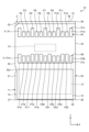
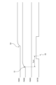
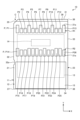
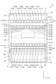
図1は、第1の実施形態に係るメモリーカード10を示す例示的な平面図である。図2は、第1の実施形態のメモリーカード10を示す例示的な側面図である。メモリーカード10は、半導体記憶装置の一例であり、例えば、リムーバブルメディア及びリムーバブルメモリーカードとも称され得る。
FIG. 1 is an exemplary plan view showing a
各図面に示されるように、本明細書において、X軸、Y軸及びZ軸が定義される。X軸とY軸とZ軸とは、互いに直交する。X軸は、メモリーカード10の幅に沿う。Y軸は、メモリーカード10の長さに沿う。Z軸は、メモリーカード10の厚さに沿う。
As shown in each drawing, an X-axis, a Y-axis, and a Z-axis are defined in this specification. The X-axis, the Y-axis, and the Z-axis are mutually perpendicular. The X-axis is along the width of the
メモリーカード10は、筐体11と、基板12と、フラッシュメモリ13と、カードコントローラ14と、保護シート15とを有する。フラッシュメモリ13は、メモリの一例である。カードコントローラ14は、コントローラの一例である。
The
メモリーカード10、及び筐体11は、例えば、Y軸方向に延びた略矩形の板状に形成される。Y軸方向は、メモリーカード10及び筐体11の長手方向であって、Y軸の正方向(Y軸の矢印が示す方向)とY軸の負方向(Y軸の矢印の反対方向)とを含む。Y軸方向は、第2の方向の一例である。
The
図2に示すように、筐体11は、板状であって、第1の面21と、第2の面22と、外縁23とを有する。第1の面21及び第2の面22は、Y軸方向に延びた略四角形(矩形)状に形成される。すなわち、Y軸方向は、第1の面21及び第2の面22の長手方向でもある。本実施形態において、メモリーカード10、筐体11、第1の面21、及び第2の面22の形状はそれぞれ、矩形状と表現されるが、他の表現もされ得る。
As shown in FIG. 2, the
第1の面21は、Z軸の正方向(Z軸の矢印が向く方向)に向く略平坦な面である。図1に示すように、第1の面21に、複数の開口21aが設けられる。図2に示すように、第2の面22は、第1の面21の反対側に位置し、Z軸の負方向(Z軸の矢印の反対方向)に向く略平坦な面である。
The
外縁23は、第1の面21と第2の面22との間に設けられ、第1の面21の縁と第2の面22の縁とに接続される。図1に示すように、外縁23は、第1の縁31と、第2の縁32と、第3の縁33と、第4の縁34と、第1の角部35と、第2の角部36と、第3の角部37と、第4の角部38とを有する。
The
第1の縁31は、X軸方向に延び、Y軸の正方向に向く。X軸方向は、メモリーカード10、筐体11、第1の面21、及び第2の面22の短手方向であって、X軸の正方向(X軸の矢印が示す方向)と、X軸の負方向(X軸の矢印の反対方向)とを含む。X軸方向は、第1の方向の一例である。
The
第2の縁32は、Y軸方向に延び、X軸の負方向に向く。第2の縁32には、凹部32aが設けられる。第3の縁33は、第2の縁32の反対側に位置してY軸方向に延び、X軸の正方向に向く。第4の縁34は、第1の縁31の反対側に位置してX軸方向に延び、Y軸の負方向に向く。
The
第2の縁32及び第3の縁33のそれぞれの長さは、第1の縁31及び第4の縁34のそれぞれの長さよりも長い。第1の縁31及び第4の縁34は、略矩形のメモリーカード10の短辺を形成し、第2の縁32及び第3の縁33は、略矩形のメモリーカード10の長辺を形成する。
The length of each of the
第1の角部35は、第1の縁31と第2の縁32との間の角部分であり、第1の縁31のX軸の負方向における端と、第2の縁32のY軸の正方向における端とを接続する。第1の縁31のX軸の負方向における端は、第1の縁の一方の端の一例である。第2の縁32のY軸の正方向における端は、第2の縁の端の一例である。
The
第1の角部35は、第1の縁31のX軸の負方向における端と、第2の縁32のY軸の正方向における端との間で直線状に延びる。X軸方向において、第1の縁31のX軸の負方向における端と、第2の縁32との間の距離は、1.1mmである。Y軸方向において、第2の縁32のY軸の正方向における端と、第1の縁31との間の距離は、1.1mmである。
The
第1の縁31と第2の縁32との角が、いわゆるC1.1の角面取りに設定されることで、第1の角部35が設けられる。別の表現によれば、第1の角部35は、第1の縁31と第2の縁32との間の切欠きCを形成する。
The corner between the
本実施形態において、第1の角部35は、互いに直交する方向に延びる第1の縁31と第2の縁32との角部分に略三角形の切欠きCを形成する。しかし、切欠きCは、この例に限られない。第1の角部35は、例えば、本実施形態よりも筐体11の内側に窪んだ略四角形の切欠きCを形成しても良い。
In this embodiment, the
第2の角部36は、第1の縁31と第3の縁33との間の角部分であり、第1の縁31のX軸の正方向における端と、第3の縁33のY軸の正方向における端とを接続する。第1の縁31のX軸の正方向における端は、第1の縁の他方の端の一例である。第3の縁33のY軸の正方向における端は、第3の縁の端の一例である。
The
第2の角部36は、第1の縁31のX軸の正方向における端と、第3の縁33のY軸の正方向における端との間で円弧状に延びる。第2の角部36は、正円の円弧状に延びるが、楕円の円弧状に延びても良い。
The
円弧状に延びる第2の角部36の半径は、0.2mmである。第1の縁31と第3の縁33との角が、いわゆるR0.2の丸面取りに設定されることで、第2の角部36が設けられる。このように、第1の角部35の形状と第2の角部36の形状とは、互いに異なる。
The radius of the
第3の角部37は、第2の縁32のY軸の負方向における端と、第4の縁34のX軸の負方向における端とを接続する。第4の角部38は、第3の縁33のY軸の負方向における端と、第4の縁34のX軸の正方向における端とを接続する。第3の角部37及び第4の角部38はそれぞれ、半径が0.2mmである円弧状に延びる。
The
メモリーカード10、筐体11、第1の面21、及び第2の面22は、Y軸方向における長さが約18±0.1mmに設定され、X軸方向における長さが約14±0.1mmに設定される。すなわち、Y軸方向における第1の縁31と第4の縁34との間の距離が約18±0.1mmに設定され、X軸方向における第2の縁32と第3の縁33との間の距離が約14±0.1mmに設定される。なお、メモリーカード10、筐体11、第1の面21、及び第2の面22のX軸方向及びY軸方向の長さは、この例に限られない。
The
図2に示すように、筐体11は、傾斜部39をさらに有する。傾斜部39は、第1の面21と第1の縁31との間の角部分であり、第1の面21のY軸の正方向における端と、第1の縁31のZ軸の正方向における端との間で直線状に延びる。
As shown in FIG. 2, the
図1に示すように、基板12、フラッシュメモリ13、及びカードコントローラ14は、筐体11の内部に設けられる。基板12、フラッシュメモリ13、及びカードコントローラ14は、箱型の筐体11に収容されても良いし、筐体11に埋め込まれても良い。
As shown in FIG. 1, the
基板12は、例えばプリント回路板(PCB)である。なお、基板12は他の種類の基板であっても良い。フラッシュメモリ13及びカードコントローラ14は、基板12に実装される。
The
フラッシュメモリ13は、情報を記憶可能な不揮発性メモリであり、例えば、NAND型フラッシュメモリである。なお、フラッシュメモリ13は、NOR型のような他のフラッシュメモリであっても良い。メモリーカード10は、例えば、積層された複数のフラッシュメモリ13を有しても良い。
The
カードコントローラ14は、フラッシュメモリ13、及び当該フラッシュメモリ13を含むメモリーカード10の全体を制御可能である。例えば、カードコントローラ14は、フラッシュメモリ13へのリード/ライト制御及び外部との通信制御を行うことができる。この通信制御には、PCIe(Peripheral Component Interconnect express)で規格(以下、単にPCIeと称する)に対応したプロトコル制御が含まれる。なお、カードコントローラ14は、フラッシュメモリ13を制御する他の電子部品を介して、フラッシュメモリ13を間接的に制御しても良い。
The
保護シート15は、第1の面21に貼り付けられる。保護シート15は、例えば、第1の面21に露出するテスト用の端子を封印する。なお、保護シート15はこの例に限られない。
The
メモリーカード10は、複数の端子Pをさらに有する。本実施形態において、メモリーカード10は、26個の端子Pを有する。なお、端子Pの数はあくまで一例であって、この例に限られない。すなわち、端子Pの数は、26個より少なくても良いし、26個より多くても良い。複数の端子Pは、例えば、基板12に設けられる。複数の端子Pは、開口21aにより、第1の面21で露出される。本実施形態において、第2の面22は、端子Pが設けられず、例えば印刷面や放熱面に利用され得る。
The
本実施形態において、複数の端子Pは、二列に並べられ、第1の列R1と、第2の列R2とを形成する。なお、複数の端子Pは、三列以上に並べられ、複数の第2の列R2を形成しても良い。 In this embodiment, the multiple terminals P are arranged in two rows, forming a first row R1 and a second row R2. Note that the multiple terminals P may be arranged in three or more rows, forming multiple second rows R2.
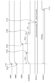
13個の端子Pが、互いに間隔を介してX軸方向に並べられ、第1の列R1を形成する。以下、第1の列R1を形成する13個の端子Pを、端子P1~P13と個別に称することがある。なお、第1の列R1を形成する端子Pの数は、13個に限られない。第1の列R1を形成する端子Pは、最も第2の縁32に近い端子P1から順に、最も第3の縁33に近い端子P13まで並べられる。
The 13 terminals P are arranged in the X-axis direction with a gap between them to form a first row R1. Hereinafter, the 13 terminals P that form the first row R1 may be individually referred to as terminals P1 to P13. Note that the number of terminals P that form the first row R1 is not limited to 13. The terminals P that form the first row R1 are arranged in order from terminal P1, which is closest to the
端子P1~P13は、第1の縁31の近傍で、当該第1の縁31に沿ってX軸方向に並べられる。端子P1~P13、及び端子P1~P13によって形成される第1の列R1は、第1の縁31から離間している。しかし、第1の列R1と第1の縁31との間の距離は、第1の列R1と第4の縁34との間の距離よりも短い。なお、端子P1~P13及び第1の列R1は、第1の縁31に隣接しても良い。
The terminals P1 to P13 are arranged in the X-axis direction near the
13個の端子Pが、互いに間隔を介してX軸方向に並べられ、第2の列R2を形成する。以下、第2の列R2を形成する13個の端子Pを、端子P14~P26と個別に称することがある。なお、第2の列R2を形成する端子Pの数は、13個に限られない。また、第2の列R2を形成する端子Pの数は、第1の列R1を形成する端子Pの数より多くても良いし少なくても良い。第2の列R2を形成する端子Pは、最も第2の縁32に近い端子P14から順に、最も第3の縁33に近い端子P26まで並べられる。
The 13 terminals P are arranged in the X-axis direction with a gap between them to form a second row R2. Hereinafter, the 13 terminals P forming the second row R2 may be individually referred to as terminals P14 to P26. The number of terminals P forming the second row R2 is not limited to 13. The number of terminals P forming the second row R2 may be more or less than the number of terminals P forming the first row R1. The terminals P forming the second row R2 are arranged in order from terminal P14, which is closest to the
第2の列R2を形成する複数の端子Pは、第1の列R1よりも第1の縁31から離れた位置で並べられる。このため、第2の列R2は、第1の列R1よりも第1の縁31から離れている。第1の列R1と第2の列R2とは、間隔を介してY軸方向に並べられる。
The multiple terminals P forming the second row R2 are arranged at a position farther from the
上述のように、複数の端子Pは、X軸方向に並べられる。この場合、一つの端子Pの少なくとも一部は、Y軸方向において、隣接する他の端子PのY軸の正方向における端とY軸の負方向における端との間の領域に位置する。第1の列R1及び第2の列R2のそれぞれにおいて、一つの端子Pが、他の端子PのY軸の正方向における端よりもY軸の正方向に張り出しても良いし、他の端子PのY軸の負方向における端よりもY軸の負方向に張り出しても良い。すなわち、各端子Pの位置は、Y軸方向にずれても良い。同じ列R1,R2の各端子PのY軸の負方向の端を揃えることで、コネクタのコンタクト位置をY軸方向に揃えた場合に各端子Pの電気的特性を類似させることができる。 As described above, the multiple terminals P are arranged in the X-axis direction. In this case, at least a part of one terminal P is located in the Y-axis direction in the region between the end in the positive direction of the Y-axis and the end in the negative direction of the Y-axis of the adjacent other terminal P. In each of the first row R1 and the second row R2, one terminal P may protrude in the positive direction of the Y-axis from the end in the positive direction of the Y-axis of the other terminal P, or may protrude in the negative direction of the Y-axis from the end in the negative direction of the Y-axis of the other terminal P. In other words, the position of each terminal P may be shifted in the Y-axis direction. By aligning the ends in the negative direction of the Y-axis of each terminal P in the same row R1 and R2, the electrical characteristics of each terminal P can be made similar when the contact positions of the connector are aligned in the Y-axis direction.
複数の端子Pは、互いに異なる形状を有しても良い。例えば、第1の列R1において、端子P1,P4,P7,P10,P13の形状と、端子P2,P3,P5,P6,P8,P9,P11,P12の形状とは、互いに異なる。さらに、第2の列R2において、端子P14,P17,P18,P19,P21,P24,P25の形状と、端子P15,P16,P20,P22,P23,P26の形状とは、互いに異なる。さらに、本実施形態において、第1の列R1及び第2の列R2のそれぞれにおいて、複数の端子Pの間の距離は略一定である。しかし、複数の端子Pの間の距離が異なっても良い。Y軸方向に装着するコネクタにおいて、メモリーカード10の電源端子やグランド端子である端子P1,P4,P7,P10,P13,P14,P17,P18,P19,P21,P24,P25が、信号端子である端子P2,P3,P5,P6,P8,P9,P11,P12,P15,P16,P20,P22,P23,P26より長く設定される。これにより、コネクタと電源端子及びグランド端子とが最初に接触するため、電気的に安定になり、信号端子に電気的ストレスを与えることを回避することができる。カードコントローラ14に電源が供給される前に信号端子に電圧が印加されると後述のインターフェース回路51の入力バッファに電気的ストレスがかかってしまう。
The multiple terminals P may have different shapes. For example, in the first row R1, the shapes of terminals P1, P4, P7, P10, and P13 are different from the shapes of terminals P2, P3, P5, P6, P8, P9, P11, and P12. Furthermore, in the second row R2, the shapes of terminals P14, P17, P18, P19, P21, P24, and P25 are different from the shapes of terminals P15, P16, P20, P22, P23, and P26. Furthermore, in this embodiment, the distance between the multiple terminals P is approximately constant in each of the first row R1 and the second row R2. However, the distance between the multiple terminals P may be different. In the connector that is attached in the Y-axis direction, the terminals P1, P4, P7, P10, P13, P14, P17, P18, P19, P21, P24, and P25, which are the power terminals and ground terminals of the
複数の端子Pには、所定のインターフェース規格に準拠した通信に用いられる信号が割り当てられる。しかし、複数の端子Pに、複数のインターフェース規格に準拠した通信に用いられる信号が割り当てられても良い。 Signals used for communication conforming to a specific interface standard are assigned to the multiple terminals P. However, signals used for communication conforming to multiple interface standards may also be assigned to the multiple terminals P.
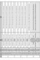
図3は、第1の実施形態の複数の端子Pの信号割り当ての一例を示す例示的な表である。図3に示すように、本実施形態において、第1の列R1の複数の端子Pには、PCIeのデータ通信に用いられる信号が割り当てられる。PCIeでは、データの通信に差動データ信号ペアを用いることができる。 Figure 3 is an exemplary table showing an example of signal assignment for multiple terminals P in the first embodiment. As shown in Figure 3, in this embodiment, signals used for PCIe data communication are assigned to multiple terminals P in the first column R1. In PCIe, differential data signal pairs can be used for data communication.
第1の列R1において、端子P1,P4,P7,P10,P13にグランド電位のグランド(GND)が割り当てられ、端子P2,P3,P8,P9に受信差動信号PERp0,PERn0,PERp1,PERn1が割り当てられ、端子P5,P6,P11,P12に送信差動信号PETp0,PETn0,PETp1,PETn1が割り当てられる。 In the first row R1, the ground potential (GND) is assigned to terminals P1, P4, P7, P10, and P13, the receive differential signals PERp0, PERn0, PERp1, and PERn1 are assigned to terminals P2, P3, P8, and P9, and the transmit differential signals PETp0, PETn0, PETp1, and PETn1 are assigned to terminals P5, P6, P11, and P12.
端子P1,P4,P7,P10,P13は、グランド端子の一例である。受信差動信号PERp0,PERn0,PERp1,PERn1及び送信差動信号PETp0,PETn0,PETp1,PETn1は、信号及び差動データ信号の一例である。端子P2,P3,P5,P6,P8,P9,P11,P12は、信号端子、第1の信号端子、及び差動データ信号端子の一例である。 The terminals P1, P4, P7, P10, and P13 are examples of ground terminals. The receive differential signals PERp0, PERn0, PERp1, and PERn1 and the transmit differential signals PETp0, PETn0, PETp1, and PETn1 are examples of signals and differential data signals. The terminals P2, P3, P5, P6, P8, P9, P11, and P12 are examples of signal terminals, first signal terminals, and differential data signal terminals.
受信差動信号PERp0,PERn0が割り当てられた一対の端子P2,P3は、二つの端子P1,P4の間に位置し、二つの端子P1,P4に囲まれる。送信差動信号PETp0,PETn0が割り当てられた一対の端子P5,P6は、二つの端子P4,P7の間に位置し、二つの端子P4,P7に囲まれる。 The pair of terminals P2, P3 to which the receive differential signals PERp0, PERn0 are assigned is located between the two terminals P1, P4 and is surrounded by the two terminals P1, P4. The pair of terminals P5, P6 to which the transmit differential signals PETp0, PETn0 are assigned is located between the two terminals P4, P7 and is surrounded by the two terminals P4, P7.
受信差動信号PERp1,PERn1が割り当てられた一対の端子P8,P9は、二つの端子P7,P10の間に位置し、二つの端子P7,P10に囲まれる。送信差動信号PETp1,PETn1が割り当てられた一対の端子P11,P12は、二つの端子P10,P13の間に位置し、二つの端子P10,P13に囲まれる。 The pair of terminals P8, P9 to which the receive differential signals PERp1, PERn1 are assigned are located between the two terminals P7, P10 and are surrounded by the two terminals P7, P10. The pair of terminals P11, P12 to which the transmit differential signals PETp1, PETn1 are assigned are located between the two terminals P10, P13 and are surrounded by the two terminals P10, P13.
PCIeでは、データをシリアル伝送するが、受信回路でクロックを生成できるようにするためと、データに同じ論理レベルが連続することで電圧レベルがハイレベル又はローレベルに偏ることを避けるために、ある単位毎にコード化される。コード化には、8B10Bや128b/130bなどの方式が用いられる。このコード化により平均信号電圧レベルがコモン電圧付近にすることができ、受信閾値レベルからの差異を少なくできる。また受信側は、データの変化点から受信クロックを生成することで、データの時間的変動に追従した受信クロックが生成できるため安定したデータ受信が可能となる。複数のレーン(差動データ信号の上り下りのペア)間で偏りがある場合でも、それぞれレーンで独立に受信回路を構成して受信データの開始位置を揃えることで、レーン間スキューをキャンセルすることができる。 In PCIe, data is transmitted serially, but is coded in units to allow the receiving circuit to generate a clock and to prevent the voltage level from being biased to high or low levels due to successive occurrences of the same logical level in the data. Methods such as 8B10B or 128b/130b are used for coding. This coding allows the average signal voltage level to be close to the common voltage, reducing the difference from the receiving threshold level. In addition, the receiving side can generate a receiving clock that tracks the temporal fluctuations of the data by generating a receiving clock from the changing point of the data, enabling stable data reception. Even if there is a bias between multiple lanes (upstream and downstream pairs of differential data signals), the skew between the lanes can be canceled by configuring independent receiving circuits for each lane and aligning the start position of the received data.
例えば、PCIe 3.0の場合の最大転送速度は1レーン当たり2Gバイト/秒(上り下りの合計)である。PCIeでは、一組の送信差動信号PETp0,PETn0及び受信差動信号PERp0,PERn0で1レーンを構成することができる。また、PCIeでは、一組の送信差動信号PETp1,PETn1及び受信差動信号PERp1,PERn1でさらに1レーンを構成することができる。このように、第1の列R1を形成する複数の端子Pに2レーンが割り当てられるため、PCIeのレーン数を増大させることができ、データ転送速度を向上させることができる。 For example, the maximum transfer speed for PCIe 3.0 is 2 GB/s per lane (upstream and downstream combined). In PCIe, one lane can be formed by a pair of transmit differential signals PETp0, PETn0 and receive differential signals PERp0, PERn0. In addition, in PCIe, one further lane can be formed by a pair of transmit differential signals PETp1, PETn1 and receive differential signals PERp1, PERn1. In this way, two lanes are assigned to the multiple terminals P that form the first row R1, so the number of PCIe lanes can be increased and the data transfer speed can be improved.
PCIeでは、初期化時に複数レーン構成を認識して、一つのデータを複数レーンで転送することができる。なお、ホスト機器が複数レーンに対応していない場合、メモリーカード10は1レーンモードで動作可能である。
PCIe recognizes a multi-lane configuration during initialization and can transfer a single piece of data over multiple lanes. If the host device does not support multiple lanes, the
端子P2,P3,P5,P6,P8,P9,P11,P12は、PCIeに準拠した差動データ信号の伝送を行い、双方向通信を可能とする。端子P2,P3,P5,P6,P8,P9,P11,P12は、周波数がGHz帯の差動データ信号を伝送する。 Terminals P2, P3, P5, P6, P8, P9, P11, and P12 transmit differential data signals conforming to PCIe, enabling bidirectional communication. Terminals P2, P3, P5, P6, P8, P9, P11, and P12 transmit differential data signals with frequencies in the GHz band.
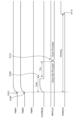
PCIeでの通信の制御に用いられる制御信号が、第2の列R2の複数の端子Pに割り当てられる。第2の列R2において、端子P14,P17にGNDが割り当てられ、端子P15,P16にレファレンス差動クロック信号REFCLKp,REFCLKnが割り当てられ、端子P18,P19に第2の電源(パワーレール)PWR2が割り当てられ、端子P20にリセット信号PERST#が割り当てられ、端子P21に第1の電源(パワーレール)PWR1が割り当てられ、端子P22にパワーマネジメント制御信号CLKREQ#が割り当てられ、端子P23,P26に制御信号CNTA,CNTBが割り当てられ、端子P24,P25に第3の電源(パワーレール)PWR3が割り当てられる。 Control signals used to control communication via PCIe are assigned to multiple terminals P in the second column R2. In the second column R2, GND is assigned to terminals P14 and P17, reference differential clock signals REFCLKp and REFCLKn are assigned to terminals P15 and P16, a second power supply (power rail) PWR2 is assigned to terminals P18 and P19, a reset signal PERST# is assigned to terminal P20, a first power supply (power rail) PWR1 is assigned to terminal P21, a power management control signal CLKREQ# is assigned to terminal P22, control signals CNTA and CNTB are assigned to terminals P23 and P26, and a third power supply (power rail) PWR3 is assigned to terminals P24 and P25.
端子P15,P16,P20,P22,P23,P26は、信号端子及び第2の信号端子の一例である。端子P15,P16は、差動クロック信号端子の一例である。端子P20,P22,P23,P26は、シングルエンド信号端子の一例である。端子P20,P22は、サイドバンド信号端子の一例である。端子P18,P19,P21,P24,P25は、電源端子の一例である。端子P18,P19は、第2の電源端子の一例である。P21は、第1の電源端子の一例である。端子P24,P25は、第3の電源端子の一例である。電源端子として複数の端子Pが設けられることにより、電流が分散し、一つの端子当たりに流れる電流が小さくなり、電源回路から電源端子までの間に存在する抵抗成分によるドロップ電圧を小さくすることができる。 Terminals P15, P16, P20, P22, P23, and P26 are examples of signal terminals and second signal terminals. Terminals P15 and P16 are examples of differential clock signal terminals. Terminals P20, P22, P23, and P26 are examples of single-ended signal terminals. Terminals P20 and P22 are examples of sideband signal terminals. Terminals P18, P19, P21, P24, and P25 are examples of power supply terminals. Terminals P18 and P19 are examples of second power supply terminals. P21 is an example of a first power supply terminal. Terminals P24 and P25 are examples of a third power supply terminal. By providing multiple terminals P as power supply terminals, the current is dispersed, the current flowing per terminal is reduced, and the drop voltage due to the resistance component existing between the power supply circuit and the power supply terminals can be reduced.
レファレンス差動クロック信号REFCLKp/nは、2本で差動クロック信号を構成する。ホスト機器から端子P15,P16に周波数がMHz帯のクロック信号を伝送されることにより、メモリーカード10は、当該メモリーカード10が装着されたホスト機器との同期を容易化することができる。このように、端子P15,P16が伝送に用いられるクロック信号の周波数は、端子P2,P3,P5,P6,P8,P9,P11,P12が伝送に用いられる差動データ信号の周波数よりも低くし正弦波に近い波形にすることでEMIの発生を低くできる。
Two reference differential clock signals REFCLKp/n make up a differential clock signal. By transmitting a clock signal with a frequency in the MHz range from the host device to terminals P15 and P16,
ホスト機器は、例えば、パーソナルコンピュータのような情報処理装置、携帯電話、デジタルカメラ、撮像装置、タブレットコンピュータやスマートフォンのような携帯端末、ゲーム機器、カーナビゲーションシステムのような車載端末、又は他の装置である。 The host device may be, for example, an information processing device such as a personal computer, a mobile phone, a digital camera, an imaging device, a mobile terminal such as a tablet computer or a smartphone, a game device, an in-vehicle terminal such as a car navigation system, or another device.
メモリーカード10は、受信したレファレンス差動クロックをPLL発振回路で逓倍してビットクロックを生成する。データはビットクロックに同期して、送信差動信号PETp0,PETn0,PETp1,PETn1から出力される。受信差動信号PERp0,PERn0,PERp1,PERn1から読み込まれたデータは、ビットクロックに同期して一つのデータとして揃えられる。つまり前記コードから生成した受信クロックにより一旦受信したデータをレファレンス差動クロックに再同期することが可能となる。
The
リセット信号PERST#は、PCIeでの通信に用いられるバスをホスト機器がリセットするために用いることができる。PCIeのリセット解除のタイミング規定によりPCIe差動レーンの初期化開始タイミングが規定される。このリセット信号PERST#は、エラー発生時などにホスト機器がメモリーカード10の再初期化を行う時に用いることができる。
The reset signal PERST# can be used by the host device to reset the bus used for PCIe communication. The timing for starting initialization of the PCIe differential lanes is regulated by the timing regulation for PCIe reset release. This reset signal PERST# can be used by the host device to reinitialize the
パワーマネジメント制御信号CLKREQ#は、パワーセービングモードから復帰するためのクロックとして用いることができる。パワーセービングモードでは、データ転送に用いられる高周波ビットクロックを停止させることで、消費電力を低減することができる。 The power management control signal CLKREQ# can be used as a clock to return from power saving mode. In power saving mode, power consumption can be reduced by stopping the high frequency bit clock used for data transfer.
制御信号CNTA,CNTBは、種々の機能を制御するため用いられ得る。例えば後述するように、PCIeの初期化に電源電圧PWR3が必要か、電源電圧PWR2が必要か、電源電圧PWR1だけで動作可能かを判別できるようにするため、制御信号CNTBを用いることができる。 The control signals CNTA and CNTB can be used to control various functions. For example, as described below, the control signal CNTB can be used to determine whether power supply voltage PWR3, power supply voltage PWR2, or power supply voltage PWR1 alone is required for PCIe initialization.
リセット信号PERST#、パワーマネジメント制御信号CLKREQ#、及び制御信号CNTA,CNTBは、シングルエンド信号である。また、リセット信号PERST#及びパワーマネジメント制御信号CLKREQ#は、PCIeのサイドバンド信号である。 The reset signal PERST#, the power management control signal CLKREQ#, and the control signals CNTA and CNTB are single-ended signals. In addition, the reset signal PERST# and the power management control signal CLKREQ# are PCIe sideband signals.
メモリーカード10がPCIeでの通信をサポートすることにより、PCIeの標準的な物理層(PHY:Physical Layer)を用いることができる。このため、メモリーカード10のデータの転送速度を上げるための設計の容易化と開発コストの低減を図ることができる。
By supporting PCIe communications, the
さらに、メモリーカード10がPCIeでの通信をサポートすることにより、PCIeのデータリンク層にNVMe(Non Volatile Memory express)を採用することができる。このため、データ転送時のオーバーヘッドを低減させることができ、データ転送効率を向上させることができる。
Furthermore, since the
ホスト機器は、端子P21に、第1の電源としての電源電圧PWR1を供給することができる。電源電圧PWR1は、本実施形態において、3.3Vに設定される。電源電圧表記は中央値を示し、ある程度の電圧変動幅は許容されている。電源電圧PWR1は、例えば、2.5V以上3.3V以下の範囲に設定され得るが、この例に限られない。 The host device can supply a power supply voltage PWR1 as a first power supply to terminal P21. In this embodiment, the power supply voltage PWR1 is set to 3.3 V. The power supply voltage notation indicates the median value, and a certain degree of voltage fluctuation is allowed. The power supply voltage PWR1 can be set in the range of 2.5 V or more and 3.3 V or less, for example, but is not limited to this example.
ホスト機器は、端子P18,P19に、第2の電源としての電源電圧PWR2を供給することができる。電源電圧PWR2は、第2の電源電圧の一例である。電源電圧PWR2は、本実施形態において、1.8Vに設定される。すなわち、電源電圧PWR2は、電源電圧PWR1以下である。電源電圧PWR2は、例えば、1.2V以上1.8V以下の範囲に設定され得るが、この例に限られない。 The host device can supply a power supply voltage PWR2 as a second power supply to terminals P18 and P19. The power supply voltage PWR2 is an example of a second power supply voltage. In this embodiment, the power supply voltage PWR2 is set to 1.8 V. That is, the power supply voltage PWR2 is equal to or lower than the power supply voltage PWR1. The power supply voltage PWR2 can be set in the range of, for example, 1.2 V or higher and 1.8 V or lower, but is not limited to this example.
ホスト機器は、端子P24、P25に、第3の電源としての電源電圧PWR3を供給することができる。電源電圧PWR3は、第1の電源電圧の一例である。電源電圧PWR3は、本実施形態において、1.2Vに設定される。すなわち、電源電圧PWR3は、電源電圧PWR2以下である。電源電圧PWR3は、この例に限られない。 The host device can supply a power supply voltage PWR3 as a third power supply to terminals P24 and P25. The power supply voltage PWR3 is an example of a first power supply voltage. In this embodiment, the power supply voltage PWR3 is set to 1.2 V. That is, the power supply voltage PWR3 is equal to or lower than the power supply voltage PWR2. The power supply voltage PWR3 is not limited to this example.
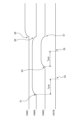
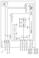
図4は、第1の実施形態のメモリーカード10の配線を模式的に示す例示的な平面図である。図4に示すように、カードコントローラ14は、第1の列R1と第2の列R2との間に位置する。なお、カードコントローラ14は、他の位置に配置されても良く、例えば、第1の列R1に含まれる端子PのY軸の正方向の端と、第2の列R2に含まれる端子PのY軸の負方向の端と、の間に位置する。また、カードコントローラ14は、当該カードコントローラ14のY軸の正方向の端とY軸の負方向の端との間に第2の列R2に含まれる端子Pが位置するように配置されても良い。
FIG. 4 is an exemplary plan view showing the wiring of the
カードコントローラ14は、複数の接続端子CPを有する。複数の接続端子CPは、受信差動信号PERp0,PERn0,PERp1,PERn1及び送信差動信号PETp0,PETn0,PETp1,PETn1が割り当てられたカードコントローラ14の端子である。複数の接続端子CPは、カードコントローラ14の一部の辺14a設けられ、第1の列R1と第2の列R2との間に位置する。接続端子CPは、端子Pとの間の配線が交差しないように配置することが望ましい。
The
メモリーカード10は、複数の配線Wと、複数のグランドプレーン41と、複数の電源配線42と、複数のESD保護ダイオード43とをさらに有する。図4は説明のため、カードコントローラ14と、端子Pと、配線Wと、グランドプレーン41と、電源配線42と、ESD保護ダイオード43とを同一平面に模式的に示す。また、図4は説明のため、グランドプレーン41と電源配線42とにハッチングを付す。
The
本実施形態において、複数の端子Pは、複数の配線W、複数のグランドプレーン41、及び複数の電源配線42が互いに重ならないように割り当てられる。このため、配線W、グランドプレーン41、電源配線42は、ビアホール無しに効率良く配線される。
In this embodiment, the multiple terminals P are assigned so that the multiple wirings W, the multiple ground planes 41, and the
複数の配線Wは、カードコントローラ14の接続端子CPと、端子P2,P3,P5,P6,P8,P9,P11,P12とを接続する配線W2,W3,W5,W6,W8,W9,W11,W12を含む。さらに、複数の配線Wは、カードコントローラ14と、端子P15,P16,P20,P22,P23,P26とを接続する配線W15,W16,W20,W22,W23,W26を含む。
The multiple wirings W include wirings W2, W3, W5, W6, W8, W9, W11, and W12 that connect the connection terminal CP of the
配線W2,W3,W5,W6,W8,W9,W11,W12の長さは、互いに等しく設定される。さらに、配線W2,W3,W5,W6,W8,W9,W11,W12は、端子P7の中心を通ってY軸方向に延びる中心軸Axに対して鏡面対称に設けられる。このため、配線W2,W3,W5,W6,W8,W9,W11,W12の設計が容易となる。また、配線W15,W16の長さは、互いに等しく設定される。 The lengths of the wires W2, W3, W5, W6, W8, W9, W11, and W12 are set to be equal to each other. Furthermore, the wires W2, W3, W5, W6, W8, W9, W11, and W12 are arranged in mirror symmetry with respect to the central axis Ax that passes through the center of the terminal P7 and extends in the Y-axis direction. This makes it easier to design the wires W2, W3, W5, W6, W8, W9, W11, and W12. Furthermore, the lengths of the wires W15 and W16 are set to be equal to each other.
配線W2,W3,W5,W6,W8,W9,W11,W12は、等長に配線し線間スキューをなくす。長さを調整するために配線を曲げる必要があるが、通常なめらかな曲線でパターンを引くことが難しいため、配線方向を変えるときは90°ではなく、複数の箇所で45°に曲げている。配線Wの幅は曲げ部分で若干広くなってしまうが、特性インピーダンスの変化が起こり、そこからノイズが発生してしまう。90°に比べ45°の方が幅の変動が少ないためノイズの発生が抑制される。 Wires W2, W3, W5, W6, W8, W9, W11, and W12 are wired at equal lengths to eliminate skew between lines. The wires need to be bent to adjust the length, but because it is usually difficult to draw a pattern with a smooth curve, they are bent at 45° in multiple places when changing the wiring direction, rather than at 90°. The width of the wire W becomes slightly wider at the bent parts, but this causes a change in the characteristic impedance, which can generate noise. There is less variation in width at 45° compared to 90°, so noise generation is suppressed.
複数のグランドプレーン41は、配線W2,W3,W5,W6,W8,W9,W11,W12,W15,W16を囲む。別の表現によれば、配線W2,W3,W5,W6,W8,W9,W11,W12,W15,W16は、複数のグランドプレーン41の間を通される。これにより、差動信号ごとにリターンパスを確保することができ、差動信号間の相互干渉を低減して作動信号レベルが安定化される。 The multiple ground planes 41 surround the wiring W2, W3, W5, W6, W8, W9, W11, W12, W15, and W16. In other words, the wiring W2, W3, W5, W6, W8, W9, W11, W12, W15, and W16 are passed between the multiple ground planes 41. This ensures a return path for each differential signal, reducing mutual interference between the differential signals and stabilizing the differential signal level.
電源配線42は、端子P18,P19,P21,P24,P25に接続される。電源配線42の幅は、配線Wの幅よりも広い。このため、電源配線42を流れることが可能な電流が大きくなるとともに、電源配線42を介した放熱が効率良く行える。また、メモリーカード10は、複数の端子Pから放熱できる。
The
ホスト電源出力とメモリーカード端子の間には配線やコネクタの抵抗成分やインダクタンス成分が存在するため電圧降下が発生する。電源電圧の許容変動範囲が、電源電圧に対して一定の割合である場合、電圧が低いほど許容電圧変動幅が小さくなる。したがって前記電圧降下があるため、電源電圧が低い程ホスト機器からカード端子の電源電圧を許容電圧変動幅に収めるように電源電圧を制御することが難しくなる。 A voltage drop occurs between the host power output and the memory card terminal due to the resistance and inductance components of the wiring and connectors. If the allowable fluctuation range of the power supply voltage is a fixed percentage of the power supply voltage, the lower the voltage, the smaller the allowable voltage fluctuation range. Therefore, due to the voltage drop, the lower the power supply voltage, the more difficult it is for the host device to control the power supply voltage at the card terminal to stay within the allowable voltage fluctuation range.
一方で、ホスト機器のコネクタや、電源配線42を含む配線の抵抗値は、同一基板、同一コネクタであれば電圧にかかわらず同じ抵抗値である。このため、電源電圧が低いと、一つの端子Pに流すことができる電流値が小さくなる。
On the other hand, the resistance of the wiring, including the host device connector and the
本実施形態では、電源電圧PWR2は、二つの端子P18,P19に流される。さらに、電源電圧PWR3は、二つの端子P24,P25に流される。このように、複数の端子P18,P19,P24,P25に電流が分配され、一つの端子Pあたりの電流値が小さくされることで、電源配線42やホスト機器のコネクタの抵抗成分によるドロップ電圧を小さくすることができる。従って、ホスト機器が電源電圧を許容電圧変動幅に収めやすくなる。さらに、電源電圧PWR2,PWR3が同じ電圧に設定することで、より大きな電流を供給することができる。
In this embodiment, the power supply voltage PWR2 is applied to two terminals P18 and P19. Furthermore, the power supply voltage PWR3 is applied to two terminals P24 and P25. In this way, the current is distributed to multiple terminals P18, P19, P24, and P25, and the current value per terminal P is reduced, thereby reducing the drop voltage due to the resistance components of the
また、通常PWR1は3.3V±5%、PWR2は1.8V±5%であるが、上述のように、電源電圧PWR1が2.5-5%~3.3V+5%のように下側により広い電圧レンジに設定され、電源電圧PWR2が1.2-5%~1.8V+5%のように下側により広い電圧レンジに設定しても良い。これにより、電圧を下げて消費電力を低減することが可能となる。 Also, normally PWR1 is 3.3V±5% and PWR2 is 1.8V±5%, but as mentioned above, power supply voltage PWR1 may be set to a wider voltage range on the lower side, such as 2.5-5% to 3.3V+5%, and power supply voltage PWR2 may be set to a wider voltage range on the lower side, such as 1.2-5% to 1.8V+5%. This makes it possible to lower the voltage and reduce power consumption.
ESD保護ダイオード43は、配線W2,W3,W5,W6,W8,W9,W11,W12のそれぞれと、グランドプレーン41とを接続する。ESD保護ダイオード43は、端子Pと接続端子CPとの間に配置され、端子P2,P3,P5,P6,P8,P9,P11,P12から侵入する静電気を吸収する。
The
複数の接続端子CPが第1の列R1と第2の列R2との間に位置することで、配線W2,W3,W5,W6,W8,W9,W11,W12は、他の配線や他の部品を迂回したり、第2の列R2に含まれる複数の端子Pの間を通過したりすることが無いように設定可能となる。このため、配線W2,W3,W5,W6,W8,W9,W11,W12の長さを短くすることができるとともに、ESD保護ダイオード43を効果的に配置可能である。本実施形態では、ESD保護ダイオード43は、第1の列R1に含まれる端子Pの近傍に配置される。
By positioning the multiple connection terminals CP between the first row R1 and the second row R2, the wiring W2, W3, W5, W6, W8, W9, W11, and W12 can be set so as not to detour around other wiring or other components, or pass between the multiple terminals P included in the second row R2. This allows the length of the wiring W2, W3, W5, W6, W8, W9, W11, and W12 to be shortened, and the
メモリーカード10は、ホスト機器のコネクタに装着される。例えば、メモリーカード10は、プッシュプルのコネクタのスロットに挿入されることで、当該コネクタに装着される。なお、メモリーカード10は、他のタイプのコネクタに装着されても良い。
The
本実施形態のメモリーカード10は、切欠きCが設けられる図1の第1の縁31から、コネクタのスロットに挿入される。これにより、メモリーカード10がコネクタに装着された状態において、第1の縁31は、第4の縁34よりもコネクタの奥に位置する。
The
第1の角部35が第1の縁31と第2の縁32との間に切欠きCを形成することで、メモリーカード10が表裏逆にコネクタのスロットに挿入されることが防止される。例えば、メモリーカード10が正しい向きでコネクタのスロットに挿入されると、切欠きCがコネクタの内部の部材を避ける。一方、メモリーカード10が表裏逆にコネクタのスロットに挿入されると、コネクタの内部の部材が、例えば第2の角部36に干渉し、メモリーカード10が完全に挿入されることを妨げる。また、Y軸方向を逆向きに、第4の縁からメモリーカード10をコネクタに挿したときも、同様にメモリーカード10はコネクタに装着できない。第1の縁31と第3の縁33との間に形成される第2の角部36付近において、X軸方向の縁とY軸方向の縁がコネクタに密着することにより、コネクタとメモリーカード10の回転方向のズレを少なくすることができる。
The
メモリーカード10がコネクタに挿入されると、コネクタのリードフレームが、複数の端子Pのそれぞれに接触する。メモリーカード10に傾斜部39が設けられ、メモリーカード10の先端がテーパ状になっている。このため、リードフレームが傾斜部39にガイドされることができ、例えば、リードフレームと筐体11との間の摩擦が低減される。従って、リードフレームのメッキが剥離することが抑制され、コネクタの耐摩耗性が向上する。
When the
リードフレームが端子Pに接触すると、ホスト機器のコントローラ(以下、ホストコントローラと称する)と、メモリーカード10のカードコントローラ14とが、ホスト機器の配線や、メモリーカード10の配線Wを介して電気的に接続される。
When the lead frame contacts the terminal P, the controller of the host device (hereinafter referred to as the host controller) and the
ホスト機器の基板に実装するためのコネクタの端子のような、コネクタのホストコントローラ側の接続点は、一般的に、コネクタのスロットの奥側(図1の上方向)に設けられる。このため、第1の列R1を形成する端子P及びリードフレームの接触点と、ホストコントローラとの間の配線の長さは、より短くされやすい。一方、第2の列R2を形成する端子P及びリードフレームの接触点と、ホストコントローラとの間の配線の長さは、例えば、第1の列R1を迂回するため、より長くなりやすい。 The connection points on the host controller side of the connector, such as the terminals of the connector for mounting on the board of the host device, are generally provided at the back side of the connector slot (upward in Figure 1). For this reason, the length of the wiring between the host controller and the contact points of the terminals P and lead frame that form the first row R1 is likely to be shorter. On the other hand, the length of the wiring between the host controller and the contact points of the terminals P and lead frame that form the second row R2 is likely to be longer, for example, because it bypasses the first row R1.
本実施形態のメモリーカード10では、ホストコントローラまでの配線長がより短くなる第1の列R1に、高速な差動データ信号の伝送を行う端子P2,P3,P5,P6,P8,P9,P11,P12が含まれるようになっている。これにより、ホスト機器の物理層(PHY)とメモリーカード10の物理層(PHY)とが近くなり、メモリーカード10の差動データ信号の伝送において、シグナルインテグリティを確保しやすくなる。
In the
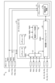
図5は、第1の実施形態のメモリーカード10の構成の第1の例を概略的に示す例示的なブロック図である。カードコントローラ14は、インターフェース回路(I/F)51と、物理層及びメモリコントローラ52と、二つのレギュレータ53,54と、電源チェック回路55とを有する。カードコントローラ14の物理層及びメモリコントローラ52は、図5において一つのブロックに示されるとともに、以下でも一体的に説明される。
Figure 5 is an exemplary block diagram that shows a first example of the configuration of the
I/F51は、シングルエンド信号に対応することができる。I/F51には、例えば、入力バッファ及び出力バッファが設けられる。入力バッファには、端子P20,P22,P23から、リセット信号PERST#、パワーマネジメント制御信号CLKREQ#、及び制御信号CNTAを入力することができる。出力バッファは、端子P22,P26を通じて、パワーマネジメント制御信号CLKREQ#に対するレスポンス及び制御信号CNTBを出力することができる。 I/F51 can handle single-ended signals. I/F51 is provided with, for example, an input buffer and an output buffer. The input buffer can input a reset signal PERST#, a power management control signal CLKREQ#, and a control signal CNTA from terminals P20, P22, and P23. The output buffer can output a response to the power management control signal CLKREQ# and a control signal CNTB via terminals P22 and P26.
物理層及びメモリコントローラ52は、差動信号に対応することができる。物理層及びメモリコントローラ52には、レシーバ及びトランスミッタが設けられる。レシーバには、受信差動信号PERp0,PERn0,PERp1,PERn1を入力することができる。トランスミッタは、送信差動信号PETp0,PETn0,PETp1,PETn1を出力することができる。
The physical layer and
物理層及びメモリコントローラ52と、電源チェック回路55とは、I/F51に接続される。物理層及びメモリコントローラ52は、フラッシュメモリ13に接続される。カードコントローラ14には、PCIeの物理層の他、PCIeのデータリンク層及びトランザクション層が設けられても良い。
The physical layer and
物理層及びメモリコントローラ52は、シリアル/パラレル変換、パラレル/シリアル変換、及びデータのシンボル化などを行うことができる。当該シンボル化は、データの0又は1が連続する時に、前記8B10Bや128b/130bなどのコードの中から、0又は1が連続しないシンボルに置き換えることで、同じ値の連続回数を所定値以下に抑える処理である。このシンボル化により、データ伝送時の電圧レベルの偏りを抑えることができる。また、同一シンボルパターンを繰り返し転送すると、特定の周波数の高周波が大きくなってしまうが、繰り替えしパターンにならないようにパターンが異なる複数のシンボルに切り替えることで、特定の周波数の高調波が大きくならないようにすることができる。つまり、EMI(ElectroMagnetic Interference)の発生を抑えることができる。
The physical layer and
なお、PCIeのトランザクション層では、データをパケット化したり、パケットのヘッダにコマンドなどを付加したりすることができる。PCIeのデータリンク層では、トランザクション層から受けとったパケットにシーケンス番号を付加したり、CRC(Cyclic Redundancy Check)符号を付加したりすることができる。シーケンス番号は、パケットの送達確認などに用いることができる。 The PCIe transaction layer can packetize data and add commands to the packet headers. The PCIe data link layer can add sequence numbers and CRC (Cyclic Redundancy Check) codes to packets received from the transaction layer. The sequence numbers can be used to confirm packet delivery, etc.
ホスト機器からメモリーカード10にシリアルの受信差動信号PERp0,PERn0,PERp1,PERn1が送信されると、レシーバにてパラレルデータの受信信号に変換される。トランスミッタにパラレルデータの送信信号が送信されると、その送信信号がシリアルの送信差動信号PETp0,PETn0,PETp1,PETn1に変換され、ホスト機器に送信される。
When serial reception differential signals PERp0, PERn0, PERp1, and PERn1 are transmitted from the host device to the
電源電圧PWR1は、フラッシュメモリ13及びカードコントローラ14に供給される。本実施形態において、電源電圧PWR1は、フラッシュメモリ13のリード/ライトのような、フラッシュメモリ13の動作に使用される。
The power supply voltage PWR1 is supplied to the
上述のように、電源電圧PWR1は、電源電圧PWR2以上であり、且つ電源電圧PWR3以上である。電源電圧PWR1は、フラッシュメモリ13の書き込み電圧を満たすことができる。
As described above, the power supply voltage PWR1 is equal to or greater than the power supply voltage PWR2 and equal to or greater than the power supply voltage PWR3. The power supply voltage PWR1 can satisfy the write voltage of the
ホスト機器とメモリーカード10とが3.3V信号電圧で接続される場合、I/O電源に電源電圧PWR1が用いられる。図5の例のようにホスト機器とメモリーカード10とが1.8V信号電圧で接続される場合であっても、電源電圧PWR1がI/O電源として用いられても良い。これにより、メモリーカード10が高耐圧化され、カード入力回路が保護される。メモリーカード10は、例えば、電源電圧PWR1が2.5Vに設定されると2.5V耐圧、電源電圧PWR1が3.3Vに設定されれば3.3V耐圧とされ得る。
When the host device and
電源電圧PWR2は、フラッシュメモリ13及びカードコントローラ14に供給される。本実施形態において、電源電圧PWR2は、ロジック回路の電源として用いられる。また、電源電圧PWR2は、フラッシュメモリ13とカードコントローラ14との間のインターフェース電圧としても用いられる。
The power supply voltage PWR2 is supplied to the
ホスト機器とメモリーカード10とが1.8V信号電圧で接続される場合、I/O電源に電源電圧PWR2が用いられても良い。この場合、メモリーカード10は、1.8V耐圧とされ得る。
When the host device and
電源電圧PWR3は、カードコントローラ14に供給される。本実施形態において、電源電圧PWR3は、差動信号回路の物理層(PHY)やアナログ回路の電源として用いられる。
The power supply voltage PWR3 is supplied to the
一般的に、アナログ動作する差動信号回路には、ノイズの少ない電源が用いられ、デジタル電源とは分離される。本実施形態において、ホスト機器から供給される電源電圧PWR3は、十分安定化されてノイズが少ない電源である必要がある。 Generally, a low-noise power supply is used for differential signal circuits that perform analog operation, and is separated from the digital power supply. In this embodiment, the power supply voltage PWR3 supplied from the host device must be a sufficiently stabilized, low-noise power supply.
以上のように、メモリーカード10では、ノイズや電源変動の影響を低減するため、三つの電源電圧PWR1,PWR2、PWR3が分離されて供給される。すなわち、三つの電源電圧PWR1,PWR2、PWR3が用途によって使い分けられる。
As described above, in
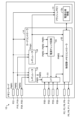
図6は、第1の実施形態のメモリーカード10の構成の第2の例を概略的に示す例示的なブロック図である。図6に示すように、電源電圧PWR2は、レギュレータ53,54に供給されても良い。さらに、電源電圧(第3の電源)PWR3が割り当てられた端子P24,P25が、グランドレベルにされても良い。これは電源電圧PWR1と電源電圧PWR2の2電源で動作するメモリーカード10を使用する場合である。
Figure 6 is an exemplary block diagram that shows a second example of the configuration of the
図6の例のように、レギュレータ54は、入力された電源電圧PWR2よりも低い電源電圧Vlogicを生成する。この電源電圧Vlogicが、電源電圧PWR2の代わりに、フラッシュメモリ13と、カードコントローラ14の物理層及びメモリコントローラ52に供給される。電源電圧Vlogicは、ロジック回路の電源として用いられるとともに、フラッシュメモリ13とカードコントローラ14との間のインターフェース電圧としても用いられる。インターフェース電圧が低減されることで、フラッシュメモリ13とカードコントローラ14との間で高速でデータ転送をすることができ、消費電力も低減される。一般に信号電圧が低い方が信号の立ち上がり/立ち下がり時間を短くできるため高速なデータ伝送が可能となる。
As shown in the example of FIG. 6, the regulator 54 generates a power supply voltage Vlogic that is lower than the input power supply voltage PWR2. This power supply voltage Vlogic is supplied to the
図6の例のように、端子P24,P25がグランド接続されると、レギュレータ53は、入力された電源電圧PWR2から、当該電源電圧PWR2よりも低い電源電圧PWR3を生成する。環境などの理由によりホスト機器から安定した電源電圧PWR3の供給が難しい場合、レギュレータ53により生成された電源電圧PWR3を用いることで問題を解消できる。
As shown in the example of FIG. 6, when terminals P24 and P25 are connected to ground,
電源電圧PWR3,Vlogicは、ともに電源電圧PWR2から生成される。電源電圧PWR3と電源電圧Vlogicとは、互いに同じ電圧でも異なった電圧でも良いが、電源分離して相互に影響しないようにするために別々なレギュレータ53及びレギュレータ54で電源電圧を生成している。また、レギュレータ53,54としてLDO(Low Drop Out)が用いられることで、入出力電圧差による無駄な消費電力を低減できる。
The power supply voltages PWR3 and Vlogic are both generated from the power supply voltage PWR2. The power supply voltages PWR3 and Vlogic may be the same or different voltages, but to separate the power supplies and prevent them from affecting each other, the power supply voltages are generated by
図6の破線で示すように、レギュレータ53が電源電圧PWR1から電源電圧PWR3を生成し、レギュレータ54が電源電圧PWR1から電源電圧Vlogicを生成しても良い。すなわち、メモリーカード10は、電源電圧PWR1があれば動作し得る。
As shown by the dashed lines in FIG. 6,
以上のように、メモリーカード10は、端子P18,P19,P21,P24,P25に印加される電源電圧PWR1、電源電圧PWR1,PWR2、又は電源電圧PWR1,PWR2,PWR3により動作し得る。メモリーカード10は、端子P18,P19,P21,P24,P25に印加される電源電圧PWR1,PWR2,PWR3の組合せに応じて、電源モードを切り替え可能であっても良い。
As described above,
ホスト機器は、以下の電源チェックシーケンスにより、フラッシュメモリ13に保存されたメモリーカード10の電源仕様情報13aを取得することで、メモリーカード10の電源構成に対応することができる。電源仕様情報13aは、例えば、電源電圧PWR1,PWR2,PWR3の電圧範囲、最大電流(連続)、及びピーク電流(100μ秒区間)を含む。
The host device can respond to the power supply configuration of the
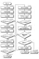
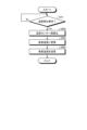
図7は、第1の実施形態のメモリーカード10の電源チェックシーケンスにおけるホスト機器の動作を示す例示的なフローチャートである。ホスト機器がフラッシュメモリ13から電源仕様情報13aを取得する前に、PCIeの初期化が行われる。このため、ホスト機器は、電源チェックシーケンスにおいて、供給する電源電圧PWR1,PWR2,PWR3の組み合わせで初期化が開始可能か否かを判定する。
Figure 7 is an exemplary flowchart showing the operation of the host device in the power supply check sequence of the
図7に示すように、ホスト機器は、コネクタのスロットに挿入されたメモリーカード10の端子P18,P19に、電源電圧PWR2を供給(印加)する(S1)。
As shown in FIG. 7, the host device supplies (applies) a power supply voltage PWR2 to terminals P18 and P19 of the
図5に示すように、電源チェック回路55に、電源電圧PWR2が入力される。電源チェック回路55は、印加された電源電圧PWR2によってPCIeによる初期化が開始できる場合、CNTB=Highをドライブする。この時点でPWR1は供給されていないが、初期化を開始する前にPWR1は供給されると想定している。 As shown in FIG. 5, the power supply voltage PWR2 is input to the power supply check circuit 55. If the applied power supply voltage PWR2 allows initialization by PCIe to start, the power supply check circuit 55 drives CNTB=High. At this point, PWR1 is not supplied, but it is assumed that PWR1 will be supplied before initialization starts.
電源チェック回路55は、印加された電源電圧PWR2によってPCIeによる初期化が開始できない場合、CNTB=Lowのままとする。 If the applied power supply voltage PWR2 does not allow initialization via PCIe to begin, the power supply check circuit 55 keeps CNTB at Low.
ホスト機器は、一定時間Tpok経過後(S2)、制御信号CNTBのレベルをチェックする(S3)。電源チェック回路55は、時間Tpokの間に制御信号CNTBのレベルをLowからHighに切り替えることができる。このため、ホスト機器は、時間Tpok経過後に制御信号CNTBのレベルを一度チェックすれば良い。CNTB=Lowのままである場合(S3:No)、ホスト機器は、メモリーカード10の端子P24,P25に電源電圧PWR3を供給(印加)する(S4)。 After a certain time Tpok has elapsed (S2), the host device checks the level of the control signal CNTB (S3). The power supply check circuit 55 can switch the level of the control signal CNTB from low to high during the time Tpok. Therefore, the host device only needs to check the level of the control signal CNTB once after the time Tpok has elapsed. If CNTB remains low (S3: No), the host device supplies (applies) the power supply voltage PWR3 to terminals P24 and P25 of the memory card 10 (S4).
電源チェック回路55は、印加された電源電圧PWR3によってPCIeによる初期化が開始できる場合、CNTB=Highをドライブする。この時点でPWR1は供給されていないが、初期化を開始する前にPWR1は供給されると想定している。一方、電源チェック回路55は、印加された電源電圧PWR3によってPCIeによる初期化が開始できない場合、CNTB=Lowのままとする。例えば、電源チェック回路55は、電源電圧PWR1によってPCIeによる初期化が開始可能である場合、CNTB=Lowのままとする。 The power supply check circuit 55 drives CNTB=High if PCIe initialization can be started by the applied power supply voltage PWR3. At this point, PWR1 is not supplied, but it is assumed that PWR1 will be supplied before initialization begins. On the other hand, if PCIe initialization cannot be started by the applied power supply voltage PWR3, the power supply check circuit 55 leaves CNTB=Low. For example, if PCIe initialization can be started by the power supply voltage PWR1, the power supply check circuit 55 leaves CNTB=Low.
ホスト機器は、一定時間Tpok経過後(S5)、制御信号CNTBのレベルをチェックする(S6)。CNTB=Lowのままである場合(S6:No)、ホスト機器は、印加と逆の順番で、電源電圧PWR3をオフにし(S7)、電源電圧PWR2をオフにする(S8)。この例ではカードが使わない電源をオフにしているが、カードの未使用電源は入れたままにしておくこともできる。 After a certain time Tpok has elapsed (S5), the host device checks the level of the control signal CNTB (S6). If CNTB remains at Low (S6: No), the host device turns off the power supply voltage PWR3 (S7) and then turns off the power supply voltage PWR2 (S8), in the reverse order of application. In this example, the power supplies not used by the card are turned off, but it is also possible to leave the unused power supplies of the card turned on.
制御信号CNTBのレベルチェック時にCNTB=Highであった場合(S3:Yes、S6:Yes)、又は電源電圧PWR2をオフにした場合(S8)、ホスト機器は、メモリーカード10の端子P21に電源電圧PWR1を供給(印加)する(S9)。つまり初期化を開始する前に電源電圧PWR1はいつも供給される。 If CNTB=High when checking the level of the control signal CNTB (S3: Yes, S6: Yes), or if the power supply voltage PWR2 is turned off (S8), the host device supplies (applies) the power supply voltage PWR1 to terminal P21 of the memory card 10 (S9). In other words, the power supply voltage PWR1 is always supplied before starting initialization.
上記のように、端子P21に電源電圧PWR1が印加されていない場合、端子P26に出力する制御信号CNTBは、電源チェック回路55の結果の出力に用いられる。メモリーカード10は、電源チェック回路55が電源電圧PWR1を検知すると、端子P26に出力するCNTBは別な用途の出力信号に切り替えることができる。また、制御信号CNTBは、電源電圧PWR2の信号電圧で出力されるため、電源チェックシーケンスにおいて電源電圧PWR2が最初に印加される。
As described above, when the power supply voltage PWR1 is not applied to terminal P21, the control signal CNTB output to terminal P26 is used to output the result of the power supply check circuit 55. When the power supply check circuit 55 detects the power supply voltage PWR1, the
次に、ホスト機器は、PCIeのトレーニングシーケンスを実行する(S10)。このトレーニングシーケンスにより、物理層の検出、物理層のトレーニング等が行われ、ホスト機器とメモリーカード10とが通信可能となって、MMIOレジスタが読み出せる状態となる。
Next, the host device executes a PCIe training sequence (S10). This training sequence detects the physical layer, trains the physical layer, and so on, enabling communication between the host device and
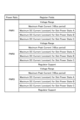
図8は、第1の実施形態の電源仕様情報13aの一例を示す例示的な表である。図8に例示される電源仕様情報13aは、電源要求仕様として記載されるレジスタ情報であり、上述のように電源電圧PWR1,PWR2,PWR3の電圧範囲、最大電流(連続)、及びピーク電流(例えば100μ秒区間)を含む。
Figure 8 is an exemplary table showing an example of power
最大電流(連続)は、メモリーカード10のメモリアクセス時に用いられる連続電流値である。ホスト機器の電源回路は、連続でこの電流値を供給することが要求される。
The maximum current (continuous) is the continuous current value used when accessing the memory of the
ピーク電流(100μ秒区間)は、例えば、100μ秒区間で測定した場合に流れるピーク電流値であり、ホスト機器の電源設定におけるカップリングコンデンサの容量や、電源回路の応答特性に影響される。ホスト機器の電源回路は、当該ピーク電流を供給可能であることが要求される。 The peak current (100 μsec interval) is, for example, the peak current value that flows when measured over a 100 μsec interval, and is affected by the capacitance of the coupling capacitor in the host device's power supply settings and the response characteristics of the power supply circuit. The host device's power supply circuit is required to be able to supply this peak current.
電圧範囲は、電源電圧が変動を許容される範囲である。ホスト機器の電源回路は、配線やコネクタのドロップ電圧が存在しても、端子Pにおける電源電圧が当該電圧範囲に入るように電圧を保持することが要求される。 The voltage range is the range within which the power supply voltage is allowed to fluctuate. The host device's power supply circuit is required to maintain the power supply voltage at terminal P within that voltage range, even if there is a drop voltage in the wiring or connectors.
さらに、電源仕様情報13aは、電源電圧PWR3がレギュレータ53によって生成されるか否かを示す情報を含む。上述のように、レギュレータ53は、端子P24,P25に電源電圧PWR3が印加されない場合、電源電圧PWR2から電源電圧PWR3を生成可能である。なお、メモリーカード10は、レギュレータ53を有していても、端子P24,P25に印加された電源電圧PWR3を用いて良い。
Furthermore, the power
図7に示すように、ホスト機器は、フラッシュメモリ13から電源仕様情報13aを読み出す(S11)。電源仕様情報13aは、例えば、MMIO上にマッピングされたNVMeレジスタのVendor Specific領域に配置されており、物理層及びメモリコントローラ52を経由して、差動データ信号で出力される。ホスト機器は、差動データ信号をデコードすることで、システムメモリ上に電源仕様情報13aを復元する。
As shown in FIG. 7, the host device reads the power
ホスト機器は、読み出した電源仕様情報13aの電源要求仕様と、当該ホスト機器の電源回路仕様とを比較して、メモリーカード10が使用可能か否かを判断する(S12)。ホスト機器が電源要求仕様を全て満足している場合(S12:Yes)、ホスト機器がフラッシュメモリ13にアクセスするための十分な電源回路を実装しているので、メモリーカード10は使用可能と判断される(S13)。
The host device compares the power requirement specifications of the read
ホスト機器が電源要求仕様を満足していない場合(S12:No)、ホスト機器は、電源電圧PWR1,PWR2,PWR3の調停が可能か否かを判断する(S14)。例えば、電源電圧PWR1が不足している場合、ホスト機器は、PCIeで定義されているSlot Power Limitで最大電力を制限することによりメモリーカード10が使用可能であれば(S14:Yes)、当該調停を行って(S15)、メモリーカード10が使用可能と判断する(S13)。一方、調停ができない場合(S14:No)、ホスト機器は、メモリーカード10を使用しない(S16)。
If the host device does not satisfy the power supply requirement specifications (S12: No), the host device determines whether arbitration of the power supply voltages PWR1, PWR2, and PWR3 is possible (S14). For example, if the power supply voltage PWR1 is insufficient, the host device performs arbitration (S15) and determines that the
メモリーカード10は、複数の電力モードを実装することができる。例えば、上述のように、メモリーカード10は、Slot Power Limit(最大消費電力の上限設定機能)を実装可能である。
The
ホスト機器は電源能力に応じて、使用可能なSlot Power LimitをPCIeパケットでメモリーカード10に設定する。例えば図8に示すように、本実施形態のメモリーカード10は、三つのSlot Power Limitをサポートした例である。なお、メモリーカード10はこの例に限られない。ピーク電流はSlot Power Limitに依存しないため、共通の設定となっている。
The host device sets the available slot power limit in the
Slot Power Limit Aは、Slot Power Limit Bよりも消費電力が大きい。また、Slot Power Limit Bは、Slot Power Limit Cよりも消費電力が大きい。消費電力が大きいほど性能は高くなる。ホスト機器の電源回路がSlot Power Limit Aを満足しない場合、Slot Power Limit Bに設定されることで、ホスト機器はメモリーカード10を使うことができる。Slot Power Limitの選択肢は、例えば、他のPCIeレジスタで与えられる。
Slot Power Limit A consumes more power than Slot Power Limit B. Slot Power Limit B also consumes more power than Slot Power Limit C. The higher the power consumption, the higher the performance. If the power supply circuit of the host device does not satisfy Slot Power Limit A, the host device can use the
図9は、第1の実施形態のメモリーカード10の電源チェックシーケンスにおける第1の例を示す例示的なタイミングチャートである。以下、図7及び図9を参照して、電源チェックシーケンスにおける第1の例を説明する。当該第1の例に係るメモリーカード10は、電源電圧PWR3を用いることで、PCIeによる初期化を開始することができる。また、図9において、図7の各動作に対応するタイミングに、当該図7に対応する符号を付与する。
Figure 9 is an exemplary timing chart showing a first example of a power supply check sequence of the
まず、ホスト機器が、メモリーカード10の端子P18,P19に電源電圧PWR2を供給する(S1)。メモリーカード10の初期化には電源電圧PWR3が用いられるので、一定時間Tpokが経過しても(S2)、制御信号CNTBのレベルはLowのままである(S3:No)。このため、ホスト機器は、メモリーカード10の端子P24,P25に電源電圧PWR3を供給する(S4)。
First, the host device supplies power supply voltage PWR2 to terminals P18 and P19 of memory card 10 (S1). Because power supply voltage PWR3 is used to initialize
電源電圧PWR3が供給されることで、CNTB=Highとなる。このため、一定時間Tpok経過後(S5)、CNTBのレベルチェック時にCNTB=Highとなっているため(S6:Yes)、ホスト機器は端子P21に電源電圧PWR1を供給する(S9)。つまり、ホストは3電源を要するメモリーカード10であると認識できる。
When power supply voltage PWR3 is supplied, CNTB becomes High. Therefore, after a certain time Tpok has elapsed (S5), CNTB becomes High when the CNTB level is checked (S6: Yes), so the host device supplies power supply voltage PWR1 to terminal P21 (S9). In other words, the host can recognize that the
図10は、第1の実施形態のメモリーカード10の電源チェックシーケンスにおける第2の例を示す例示的なタイミングチャートである。以下、図7及び図10を参照して、電源チェックシーケンスにおける第2の例を説明する。当該第2の例に係るメモリーカード10は、レギュレータ53により電源電圧PWR2から電源電圧PWR3を生成でき、電源電圧PWR2を用いることでPCIeによる初期化を開始することができる。
Figure 10 is an exemplary timing chart showing a second example of the power supply check sequence of the
まず、ホスト機器が、メモリーカード10の端子P18,P19に電源電圧PWR2を供給する(S1)。電源電圧PWR2が供給されることで、CNTB=Highとなる。このため、一定時間Tpok経過後(S2)、CNTBのレベルチェック時にCNTB=Highとなっているため(S3:Yes)、ホスト機器は端子P21に電源電圧PWR1を供給する(S9)。時間Tpokは、例えば、レギュレータ53が生成する電源電圧PWR3が安定するために十分な時間に設定される。つまり、ホストはPWR1とPWR2の2電源を要するメモリーカード10であると認識できる。
First, the host device supplies power supply voltage PWR2 to terminals P18 and P19 of memory card 10 (S1). Supplying power supply voltage PWR2 sets CNTB=High. Therefore, after a certain time Tpok has elapsed (S2), CNTB=High is found when checking the CNTB level (S3: Yes), so the host device supplies power supply voltage PWR1 to terminal P21 (S9). Time Tpok is set, for example, to a time sufficient for power supply voltage PWR3 generated by
図11は、第1の実施形態のメモリーカード10の電源チェックシーケンスにおける第3の例を示す例示的なタイミングチャートである。以下、図7及び図11を参照して、電源チェックシーケンスにおける第3の例を説明する。当該第3の例に係るメモリーカード10は、レギュレータ53により電源電圧PWR1から電源電圧PWR3を生成でき、電源電圧PWR1を用いることでPCIeによる初期化を開始することができる。
Figure 11 is an exemplary timing chart showing a third example of the power supply check sequence of the
まず、ホスト機器が、メモリーカード10の端子P18,P19に電源電圧PWR2を供給する(S1)。メモリーカード10の初期化には電源電圧PWR1が用いられるので、一定時間Tpokが経過しても(S2)、制御信号CNTBのレベルはLowのままである(S3:No)。
First, the host device supplies the power supply voltage PWR2 to terminals P18 and P19 of the memory card 10 (S1). Since the power supply voltage PWR1 is used to initialize the
ホスト機器は、メモリーカード10の端子P24,P25に電源電圧PWR3を供給する(S4)。一定時間Tpokが経過しても(S5)、制御信号CNTBのレベルはLowのままである(S6:No)。このため、ホスト機器は、電源電圧PWR3(S7)、電源電圧PWR2をオフとし(S8)、端子P21に電源電圧PWR1を供給する(S9)。つまり、ホストはPWR1の1電源を要するメモリーカード10であると認識できる。電源電圧PWR1が供給されると、メモリーカード10は、電源チェック回路55の出力は切り離されて制御信号CNTBが割り当てられた端子P26に出力されなくなるが、制御信号CNTBは別な用途の信号として使用することができる。
The host device supplies power supply voltage PWR3 to terminals P24 and P25 of memory card 10 (S4). Even after a certain time Tpok has elapsed (S5), the level of the control signal CNTB remains low (S6: No). For this reason, the host device turns off power supply voltage PWR3 (S7) and power supply voltage PWR2 (S8), and supplies power supply voltage PWR1 to terminal P21 (S9). In other words, the host can recognize that
フラッシュメモリ13に高速アクセスするために、大きな電流が用いられる場合がある。しかし、PCIeの初期化で消費される電流は、高速アクセスするための電流よりも少なくて済む。そのため最低限の電源の実装でも前記電源仕様情報13aは読み出すことができる。
A large current may be used to access the
以上の電源チェックシーケンスにおいて、メモリーカード10のカードコントローラ14は、端子P18,P19,P21,P24,P25に印加された電源電圧PWR1,PWR2,PWR3によって差動データ信号によるPCIeの初期化が可能か否かを判定して、端子P26から判定結果を出力する。さらに、フラッシュメモリ13は、差動データ信号によるPCIeの初期化が完了すると、当該フラッシュメモリ13に記録された電源仕様情報13aが読み出し可能となる。
In the above power supply check sequence, the
以上の電源チェックシーケンスにより、別々の電源仕様を有する複数の種類のメモリーカード10が混在しても、ホスト機器が当該電源仕様を識別することができる。なお、メモリーカード10と、対応するホスト機器との電源仕様を予め定めておくことで、電源チェックシーケンスを省略することができる。
The above power supply check sequence allows the host device to identify the power supply specifications even when multiple types of
ホスト機器は、例えば、コネクタに対するメモリーカード10の挿抜を検出する機能を有する。この場合、ホスト機器は、コネクタへのメモリーカード10の挿入を検出した後に電源を投入し、コネクタからメモリーカード10が抜かれたことを検出すると電源をオフにする。このため、メモリーカード10は、活線挿抜についての機能を省略できる。
The host device has a function for detecting, for example, the insertion and removal of the
以上説明された第1の実施形態に係るメモリーカード10において、筐体11は、X軸方向に延びた第1の縁31と、X軸方向と交差するY軸方向に延びた第2の縁32と、第1の縁31と第2の縁32との間の切欠きCを形成する第1の角部35とを有する。切欠きCを形成する第1の角部35は、例えば、メモリーカード10の逆挿し防止に用いられる。このため、メモリーカード10が例えばプッシュプルタイプのコネクタに挿入される場合、メモリーカード10は、第1の縁31からコネクタに挿入される。そして、複数の端子Pは、互いに間隔を介してX軸方向に並べられて第1の列R1を形成するとともに、第1の列R1よりも第1の縁31から離れた位置で互いに間隔を介してX軸方向に並べられて第2の列R2を形成する。このように、複数の端子Pが複数の列R1,R2を形成することで、本実施形態のメモリーカード10は、通信インターフェースを高速化できる。
In the
一般的に、コネクタに挿入されたメモリーカード10の端子Pとホストコントローラとの間の配線の長さは、コネクタの奥ほど短くなる。すなわち、第1の列R1に含まれる端子Pとホストコントローラとの間の配線の長さは、第2の列R2に含まれる端子Pとホストコントローラとの間の配線の長さよりも短くなる。このため、第1の列R1に含まれる信号の伝送に用いられる端子P2,P3,P5,P6,P8,P9,P11,P12は、第2の列R2に含まれる信号の伝送に用いられる端子P15,P16,P20,P22、P23,P26よりも、シグナルインテグリティを確保しやすい。例えば、第1の列R1に含まれる信号の伝送に用いられる端子Pの数を第2の列R2に含まれる信号の伝送に用いられる端子Pの数より多くしたり、第1の列R1に含まれる端子Pが差動信号の伝送に用いられたりすることで、本実施形態のメモリーカード10は、通信インターフェースを高速化できる。
In general, the length of the wiring between the terminal P of the
第1の列R1に含まれる端子P2,P3,P5,P6,P8,P9,P11,P12の数が、第2の列R2に含まれる端子P15,P16,P20,P22、P23,P26の数よりも多い。これにより、本実施形態のメモリーカード10は、通信インターフェースを高速化できる。
The number of terminals P2, P3, P5, P6, P8, P9, P11, and P12 included in the first row R1 is greater than the number of terminals P15, P16, P20, P22, P23, and P26 included in the second row R2. This allows the
さらに、複数の端子Pが、第1の列R1と第2の列R2とを形成する。これにより、複数の端子Pを一列に並べる場合に比べ、信号の伝送に用いられる端子P2,P3,P5,P6,P8,P9,P11,P12を第1の縁31の近傍により多く並べたとしても、端子Pの所望の大きさや、複数の端子Pの所望の間隔を確保することができる。
Furthermore, the multiple terminals P form a first row R1 and a second row R2. As a result, compared to arranging the multiple terminals P in a single row, even if more of the terminals P2, P3, P5, P6, P8, P9, P11, and P12 used for signal transmission are arranged near the
端子P15,P16,P20,P22、P23,P26よりも高い周波数の信号の伝送に用いられる端子P2,P3,P5,P6,P8,P9,P11,P12が、第1の列R1に含まれる。これにより、本実施形態のメモリーカード10は、通信インターフェースを高速化できる。
Terminals P2, P3, P5, P6, P8, P9, P11, and P12, which are used to transmit signals at higher frequencies than terminals P15, P16, P20, P22, P23, and P26, are included in the first row R1. This allows the
差動データ信号端子を増やしレーン数を増やすことで、本実施形態のメモリーカード10は、通信インターフェースを高速化できる。
By increasing the number of differential data signal terminals and lanes, the
第1の列R1を形成する複数の端子Pは、差動データ信号が割り当てられた端子P2,P3,P5,P6,P8,P9,P11,P12を含む。一方、第2の列R2を形成する複数の端子Pは、差動データ信号よりも低い周波数の差動クロック信号が割り当てられた端子P15,P16と、シングルエンド信号が割り当てられた端子P20,P22,P23,P26と、電源が割り当てられた端子P18,P19、P21,P24,P25とを含む。これにより、第1の列R1において、高速に信号を伝送可能な端子P2,P3,P5,P6,P8,P9,P11,P12の数をより多くすることができ、本実施形態のメモリーカード10は、通信インターフェースを高速化できる。
The multiple terminals P forming the first column R1 include terminals P2, P3, P5, P6, P8, P9, P11, and P12 to which differential data signals are assigned. On the other hand, the multiple terminals P forming the second column R2 include terminals P15 and P16 to which differential clock signals having a lower frequency than the differential data signals are assigned, terminals P20, P22, P23, and P26 to which single-ended signals are assigned, and terminals P18, P19, P21, P24, and P25 to which power is assigned. This allows the number of terminals P2, P3, P5, P6, P8, P9, P11, and P12 capable of transmitting signals at high speed in the first column R1 to be increased, and the
第1の列R1を形成する複数の端子Pは、差動データ信号の複数のレーンが割り当てられた端子P2,P3,P5,P6,P8,P9,P11,P12を含む。これにより、本実施形態のメモリーカード10は、通信インターフェースを高速化できる。
The multiple terminals P forming the first row R1 include terminals P2, P3, P5, P6, P8, P9, P11, and P12 to which multiple lanes of differential data signals are assigned. This allows the
複数対の端子P2,P3,P5,P6,P8,P9,P11,P12はそれぞれ、複数の端子P1,P4,P7,P10,P13のうち二つの間に位置する。これにより、差動信号ごとにリターンパスを確保することができ、差動信号間の相互干渉を低減して作動信号レベルが安定化される。 The multiple pairs of terminals P2, P3, P5, P6, P8, P9, P11, and P12 are each located between two of the multiple terminals P1, P4, P7, P10, and P13. This ensures a return path for each differential signal, reducing mutual interference between differential signals and stabilizing the differential signal level.
端子P20,P22は、PCIe規格のサイドバンド信号が割り当てられる。これにより、第1の列R1において、高速に信号を伝送可能な端子P2,P3,P5,P6,P8,P9,P11,P12の数をより多くすることができ、本実施形態のメモリーカード10は、通信インターフェースを高速化できる。
Terminals P20 and P22 are assigned sideband signals of the PCIe standard. This allows the number of terminals P2, P3, P5, P6, P8, P9, P11, and P12 capable of transmitting signals at high speed to be increased in the first row R1, and the
端子P21は、第1の電源PWR1が割り当てられる。端子P18,P19は、電圧が第1の電源PWR1以下である第2の電源PWR2が割り当てられる。端子P24,P25は、電圧が第2の電源PWR2以下である第3の電源PWR3が割り当てられる。これにより、第1乃至第3の電源PWR1,PWR2,PWR3を用途によって使い分けることができ、メモリーカード10のフレキシビリティが高まる。さらに、電圧が低いほど電源電圧変動の許容値が小さくなるので、ひとつの端子Pに流す電流値を小さくした方が良いが、複数の端子P18,P19と複数の端子P24,P25が設けられることで、電流値が分散されて一端子当たりの電流値が小さくなり、電圧変動が抑制される。
Terminal P21 is assigned the first power supply PWR1. Terminals P18 and P19 are assigned the second power supply PWR2, whose voltage is equal to or lower than the first power supply PWR1. Terminals P24 and P25 are assigned the third power supply PWR3, whose voltage is equal to or lower than the second power supply PWR2. This allows the first to third power supplies PWR1, PWR2, and PWR3 to be used according to the application, increasing the flexibility of the
レギュレータ53は、電源電圧PWR3の第3の電源PWR3が割り当てられた端子P24,P25がグランド接続された場合、電源電圧PWR2の第2の電源PWR2が割り当てられた端子P18,P19に印加された電源電圧PWR2から電源電圧PWR3を生成する。これにより、本実施形態のメモリーカード10は、PWR1,PWR2の2電源構成のホスト機器とPWR1,PWR2,PWR3の3電源構成のホスト機器のどちらにも対応することができる。
When terminals P24 and P25 to which the third power supply PWR3 of the power supply voltage PWR3 is assigned are grounded,
カードコントローラ14は、端子P18,P19,P21,P24,P25に印加された電源電圧PWR1,PWR2,PWR3によって差動データ信号による初期化が可能か否かを判定して、制御信号CNTBが割り当てられた端子P26から判定結果を出力する。フラッシュメモリ13は、差動データ信号による初期化が完了すると、当該フラッシュメモリ13に記憶された電源仕様情報13aが読み出し可能となる。ホスト機器は、電源仕様情報13aと、当該ホスト機器の電源仕様とを比較することにより、メモリーカード10が使用可能か否か判断できる。これにより、複数種類の電源構成を有するメモリーカード10が混在しても、ホスト機器がメモリーカード10の電源仕様を識別することができる。
The
少なくともカードコントローラ14の一部の辺14aは、第1の列R1と第2の列R2との間に位置するとともに第1の列R1に含まれる端子P2,P3,P5,P6,P8,P9,P11,P12に配線Wによって接続された接続端子CPを辺14aに有する。これにより、配線Wが他の配線や他の部品を迂回したり、第2の列R2に含まれる複数の端子Pの間を通過したりすることが無いよう設定可能となる。従って、例えばESD保護ダイオード43を配線Wに設けることが容易になるとともに、第1の列R1に含まれる端子P2,P3,P5,P6,P8,P9,P11,P12と接続端子CPとの間の配線Wの長さを短くすることができる。
At least a part of the
メモリーカード10は、X軸方向における長さが14±0.1mmであり、Y軸方向における長さが18±0.1mmである。一般的に、microSDカードの寸法は11mm×15mmである。すなわち、本実施形態のメモリーカード10は、microSDカードよりも大きい。従って、メモリーカード10は、例えば、大型の三次元フラッシュメモリのような、microSDカードに搭載困難な記憶容量及び寸法が大きいメモリを搭載することができ、例えば、技術進化による将来的なフラッシュメモリ13のサイズの大型化に対応できる。さらに、メモリーカード10は、microSDカードよりも大きく、標準のSDメモリーカードよりも小さい。このため、メモリーカード10は、ホスト機器にとって大き過ぎず、且つホスト機器のコネクタへの挿抜もしやすい。
The
筐体11は、第2の縁32の反対側に位置してY軸方向に延びた第3の縁33と、第1の縁31と第3の縁33との間の第2の角部36と、をさらに有する。第1の角部35の形状と、第2の角部36の形状とが互いに異なる。これにより、メモリーカード10の逆挿しが抑制される。
The
第1の角部35は、第1の縁31の一方の端と第2の縁32の端との間で直線状に延び、いわゆるC1.1の角面取りされた部分を形成する。第2の角部36は、第1の縁31の他方の端と第3の縁33の端との間で円弧状に延び、いわゆるR0.2の丸面取りされた部分を形成する。メモリーカード10は、第2の角部36がコネクタに当接した状態で当該コネクタに挿入されることがある。この場合に、X軸方向におけるメモリーカード10の位置ずれを小さくすることができる。
The
(第2の実施形態)
以下に、第2の実施形態について、図12を参照して説明する。なお、以下の実施形態の説明において、既に説明された構成要素と同様の機能を持つ構成要素は、当該既述の構成要素と同じ符号が付され、さらに説明が省略される場合がある。また、同じ符号が付された複数の構成要素は、全ての機能及び性質が共通するとは限らず、各実施形態に応じた異なる機能及び性質を有していても良い。
Second Embodiment
The second embodiment will be described below with reference to Fig. 12. In the following description of the embodiment, components having the same functions as components already described are given the same reference numerals as the components already described, and further description may be omitted. In addition, multiple components given the same reference numerals do not necessarily have all the same functions and properties, and may have different functions and properties according to each embodiment.
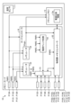
図12は、第2の実施形態に係るメモリーカード10を示す例示的な平面図である。図12に示すように、第2の実施形態に係るカードコントローラ14は、フラッシュメモリ13に積層される。
FIG. 12 is an exemplary plan view showing a
フラッシュメモリ13は、第2の列R2に含まれる端子Pに重ねられる。別の表現によれば、フラッシュメモリ13は、当該フラッシュメモリ13のY軸の正方向の端とY軸の負方向の端との間に第2の列R2に含まれる端子Pが位置するように配置される。一方、フラッシュメモリ13は、第1の列R1に含まれる端子Pから離間している。
The
カードコントローラ14は、第1の列R1と第2の列R2との間に位置する。このため、第1の実施形態と同じく、カードコントローラ14の複数の接続端子CPも、第1の列R1と第2の列R2との間に位置する。配線Wが、接続端子CPと、第1の列R1に含まれる端子Pとを接続する。
The
以上説明された第2の実施形態のメモリーカード10のように、カードコントローラ14は、フラッシュメモリ13に積層されても良い。フラッシュメモリ13が第1の列R1から離間し、接続端子CPが第1の列R1と第2の列R2との間に位置することで、配線Wの長さが長くなることが抑制される。
As in the
(第3の実施形態)
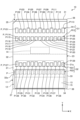
以下に、第3の実施形態について、図13乃至図25を参照して説明する。図13は、第3の実施形態に係るメモリーカード10を示す例示的な平面図である。図14は、第3の実施形態のメモリーカード10を示す例示的な側面図である。メモリーカード10は、半導体記憶装置の一例である。
Third Embodiment
The third embodiment will be described below with reference to Fig. 13 to Fig. 25. Fig. 13 is an exemplary plan view showing a
メモリーカード10は、筐体11と、基板12と、フラッシュメモリ13と、カードコントローラ14と、保護シート15とを有する。フラッシュメモリ13は、メモリの一例である。カードコントローラ14は、コントローラの一例である。
The
メモリーカード10、及び筐体11は、例えば、Y軸方向に延びた略矩形の板状に形成される。Y軸方向は、メモリーカード10及び筐体11の長手方向である。Y軸方向は、第2の方向の一例である。
The
図14に示すように、筐体11は、板状であって、第1の面21と、第2の面22と、外縁23とを有する。第1の面21及び第2の面22は、Y軸方向に延びた略四角形(矩形)状に形成される。すなわち、Y軸方向は、第1の面21及び第2の面22の長手方向でもある。本実施形態において、メモリーカード10、筐体11、第1の面21、及び第2の面22の形状はそれぞれ、矩形状と表現されるが、他の表現もされ得る。
As shown in FIG. 14, the
第1の面21は、Z軸の正方向に向く略平坦な面である。図13に示すように、第1の面21に、複数の開口21aが設けられる。図14に示すように、第2の面22は、第1の面21の反対側に位置し、Z軸の負方向に向く略平坦な面である。
The
外縁23は、第1の面21と第2の面22との間に設けられ、第1の面21の縁と第2の面22の縁とに接続される。図13に示すように、外縁23は、第1の縁31と、第2の縁32と、第3の縁33と、第4の縁34と、第1の角部35と、第2の角部36と、第3の角部37と、第4の角部38とを有する。第1の縁31は、第1の端縁の一例である。第2の縁32は、第1の側縁の一例である。第3の縁33は、第2の側縁の一例である。第4の縁34は、第2の端縁の一例である。
The
第1の縁31は、X軸方向に延び、Y軸の正方向に向く。X軸方向は、メモリーカード10、筐体11、第1の面21、及び第2の面22の短手方向であって、X軸の正方向と、X軸の負方向とを含む。X軸方向は、第1の方向の一例である。
The
第2の縁32は、Y軸方向に延び、X軸の負方向に向く。第2の縁32には、凹部32aが設けられる。第3の縁33は、第2の縁32の反対側に位置してY軸方向に延び、X軸の正方向に向く。第4の縁34は、第1の縁31の反対側に位置してX軸方向に延び、Y軸の負方向に向く。
The
第2の縁32及び第3の縁33のそれぞれの長さは、第1の縁31及び第4の縁34のそれぞれの長さよりも長い。第1の縁31及び第4の縁34は、略矩形のメモリーカード10の短辺を形成し、第2の縁32及び第3の縁33は、略矩形のメモリーカード10の長辺を形成する。
The length of each of the
第1の角部35は、第1の縁31と第2の縁32との間の角部分であり、第1の縁31のX軸の負方向における端と、第2の縁32のY軸の正方向における端とを接続する。第1の縁31のX軸の負方向における端は、第1の縁の一方の端の一例である。第2の縁32のY軸の正方向における端は、第2の縁の端の一例である。
The
第1の角部35は、第1の縁31のX軸の負方向における端と、第2の縁32のY軸の正方向における端との間で直線状に延びる。X軸方向において、第1の縁31のX軸の負方向における端と、第2の縁32との間の距離は、1.1mmである。別の表現によれば、X軸方向において、第1の縁31のX軸の負方向における端と、第1の縁31の延長線及び第2の縁32の延長線の交点との間の距離は、1.1mmである。
The
Y軸方向において、第2の縁32のY軸の正方向における端と、第1の縁31との間の距離は、1.1mmである。別の表現によれば、Y軸方向において、第2の縁32のY軸の正方向における端と、第1の縁31の延長線及び第2の縁32の延長線の交点との間の距離は、1.1mmである。
In the Y-axis direction, the distance between the end of the
第1の縁31と第2の縁32との角が、いわゆるC1.1の角面取りに設定されることで、第1の角部35が設けられる。別の表現によれば、第1の角部35は、第1の縁31と第2の縁32との間の切欠きCを形成する。
The corner between the
本実施形態において、第1の角部35は、互いに直交する方向に延びる第1の縁31と第2の縁32との角部分に略三角形の切欠きCを形成する。しかし、切欠きCは、この例に限られない。第1の角部35は、例えば、本実施形態よりも筐体11の内側に窪んだ略四角形の切欠きCを形成しても良い。
In this embodiment, the
第2の角部36は、第1の縁31と第3の縁33との間の角部分であり、第1の縁31のX軸の正方向における端と、第3の縁33のY軸の正方向における端とを接続する。第1の縁31のX軸の正方向における端は、第1の縁の他方の端の一例である。第3の縁33のY軸の正方向における端は、第3の縁の端の一例である。
The
第2の角部36は、第1の縁31のX軸の正方向における端と、第3の縁33のY軸の正方向における端との間で円弧状に延びる。第2の角部36は、正円の円弧状に延びるが、楕円の円弧状に延びても良い。
The
円弧状に延びる第2の角部36の半径は、0.2mmである。第1の縁31と第3の縁33との角が、いわゆるR0.2の丸面取りに設定されることで、第2の角部36が設けられる。このように、第1の角部35の形状と第2の角部36の形状とは、互いに異なる。
The radius of the
第3の角部37は、第2の縁32のY軸の負方向における端と、第4の縁34のX軸の負方向における端とを接続する。第4の角部38は、第3の縁33のY軸の負方向における端と、第4の縁34のX軸の正方向における端とを接続する。第3の角部37及び第4の角部38はそれぞれ、半径が0.2mmである円弧状に延びる。
The
メモリーカード10、筐体11、第1の面21、及び第2の面22は、Y軸方向における長さが約18±0.1mmに設定され、X軸方向における長さが約14±0.1mmに設定される。すなわち、Y軸方向における第1の縁31と第4の縁34との間の距離が約18±0.1mmに設定され、X軸方向における第2の縁32と第3の縁33との間の距離が約14±0.1mmに設定される。なお、メモリーカード10、筐体11、第1の面21、及び第2の面22のX軸方向及びY軸方向の長さは、この例に限られない。
The
図14に示すように、筐体11は、傾斜部39をさらに有する。傾斜部39は、第1の面21と第1の縁31との間の角部分であり、第1の面21のY軸の正方向における端と、第1の縁31のZ軸の正方向における端との間で直線状に延びる。
As shown in FIG. 14, the
図13に示すように、基板12、フラッシュメモリ13、及びカードコントローラ14は、筐体11の内部に設けられる。基板12、フラッシュメモリ13、及びカードコントローラ14は、箱型の筐体11に収容されても良いし、筐体11に埋め込まれても良い。
As shown in FIG. 13, the
基板12は、例えばPCBである。なお、基板12は他の種類の基板であっても良い。フラッシュメモリ13及びカードコントローラ14は、基板12に実装される。
The
フラッシュメモリ13は、情報を記憶可能な不揮発性メモリであり、例えば、NAND型フラッシュメモリである。なお、フラッシュメモリ13は、NOR型のような他のフラッシュメモリであっても良い。メモリーカード10は、例えば、積層された複数のフラッシュメモリ13を有しても良い。
The
カードコントローラ14は、フラッシュメモリ13、及び当該フラッシュメモリ13を含むメモリーカード10の全体を制御可能である。例えば、カードコントローラ14は、フラッシュメモリ13へのリード/ライト制御及び外部との通信制御を行うことができる。この通信制御には、PCIeに対応したプロトコル制御が含まれる。なお、カードコントローラ14は、フラッシュメモリ13を制御する他の電子部品を介して、フラッシュメモリ13を間接的に制御しても良い。
The
保護シート15は、第1の面21に貼り付けられる。保護シート15は、例えば、第1の面21に露出するテスト用の端子を封印する。なお、保護シート15はこの例に限られない。
The
メモリーカード10は、複数の端子Pをさらに有する。本実施形態において、メモリーカード10は、39個の端子Pを有する。なお、端子Pの数はあくまで一例であって、この例に限られない。すなわち、端子Pの数は、39個より少なくても良いし、39個より多くても良い。複数の端子Pは、例えば、基板12に設けられる。複数の端子Pは、開口21aにより、第1の面21で露出される。本実施形態において、第2の面22は、端子Pが設けられず、例えば印刷面や放熱面に利用され得る。
The
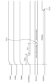
本実施形態の複数の端子Pは、第1のグループG1と、第2のグループG2と、に分けられる複数の列を形成する。第1のグループG1は、第1の列R11,R12を含む。第2のグループG2は、第2の列R21を含む。すなわち、複数の端子Pは、三列に並べられ、第1の列R11,R12及び第2の列R21を形成する。 In this embodiment, the multiple terminals P form multiple rows that are divided into a first group G1 and a second group G2. The first group G1 includes the first rows R11 and R12. The second group G2 includes the second row R21. That is, the multiple terminals P are arranged in three rows, forming the first rows R11, R12 and the second row R21.
第1のグループG1は、少なくとも一つの第1の列(R11,R12)を含む。すなわち、第1のグループG1は、一つの第1の列(R11又はR12)を含んでも良いし、二つより多い第1の列(R11,R12…)を含んでも良い。 The first group G1 includes at least one first column (R11, R12). That is, the first group G1 may include one first column (R11 or R12) or may include more than two first columns (R11, R12, ...).
第2のグループG2は、少なくとも一つの第2の列(R21)を含む。すなわち、第2のグループG2は、一つの第2の列(R21)を含んでも良いし、二つより多い第2の列(R21,R22…)を含んでも良い。 The second group G2 includes at least one second column (R21). That is, the second group G2 may include one second column (R21) or more than two second columns (R21, R22, ...).
図15は、第3の実施形態の変形例に係るメモリーカード10を示す例示的な平面図である。図15に示すように、変形例のメモリーカード10は、二列に並べられて第1の列R11及び第2の列R21を形成する26個の端子Pを有しても良い。すなわち、第1のグループG1が一つの第1の列R11を有し、第1の列R12が省略されても良い。
Figure 15 is an exemplary plan view showing a
図13に示すように、第1の列R11は、第4の縁34よりも第1の縁31に近い位置で互いに間隔を介してX軸方向に並べられた13個の端子Pを含む。以下、第1の列R11を形成し、第1の列R11に含まれる13個の端子Pを、端子P101~P113と個別に称することがある。なお、第1の列R11を形成する端子Pの数は、13個に限られない。第1の列R11を形成する端子Pは、最も第2の縁32に近い端子P101から順に、最も第3の縁33に近い端子P113まで並べられる。
As shown in FIG. 13, the first row R11 includes 13 terminals P arranged at intervals in the X-axis direction at a position closer to the
端子P101~P113は、第1の縁31の近傍で、当該第1の縁31に沿ってX軸方向に並べられる。端子P101~P113、及び端子P101~P113によって形成される第1の列R11は、第1の縁31から若干離間している。しかし、第1の列R11と第1の縁31との間の距離は、第1の列R11と第4の縁34との間の距離よりも短い。なお、端子P101~P113及び第1の列R11は、第1の縁31に隣接しても良い。
The terminals P101 to P113 are arranged in the X-axis direction near the
第1の列R12は、第4の縁34よりも第1の縁31に近い位置で互いに間隔を介してX軸方向に並べられた13個の端子Pを含む。以下、第1の列R12を形成し、第1の列R12に含まれる13個の端子Pを、端子P114~P126と個別に称することがある。なお、第1の列R12を形成する端子Pの数は、13個に限られない。また、第1の列R12を形成する端子Pの数は、第1の列R11を形成する端子Pの数より多くても良いし少なくても良い。第1の列R12を形成する端子Pは、最も第2の縁32に近い端子P114から順に、最も第3の縁33に近い端子P126まで並べられる。
The first row R12 includes 13 terminals P arranged at intervals in the X-axis direction at a position closer to the
第1の列R12を形成する複数の端子Pは、第1の列R11よりも第1の縁31から離れた位置で並べられる。このため、第1の列R12は、第1の列R11よりも第1の縁31から離れている。第1の列R11と第1の列R12とは、所定の短い間隔を介して、Y軸方向に並べられる。
The multiple terminals P forming the first row R12 are arranged at a position farther from the
第2の列R21は、第1の縁31よりも第4の縁34に近い位置で互いに間隔を介してX軸方向に並べられた13個の端子Pを含む。以下、第2の列R21を形成し、第2の列R21に含まれる13個の端子Pを、端子P127~P139と個別に称することがある。なお、第2の列R21を形成する端子Pの数は、13個に限られない。また、第2の列R21を形成する端子Pの数は、第1の列R11及び第1の列R12をそれぞれ形成する端子Pの数より多くても良いし少なくても良い。第2の列R21を形成する端子Pは、最も第2の縁32に近い端子P127から順に、最も第3の縁33に近い端子P139まで並べられる。
The second row R21 includes 13 terminals P arranged at intervals in the X-axis direction at a position closer to the
第2の列R21を形成する複数の端子Pは、第1の縁31よりも第4の縁34に近い位置にある。別の表現によれば、第2の列R21を形成する複数の端子Pは、Y軸方向におけるメモリーカード10及び筐体11の中心線(一点鎖線で示される)と、第4の縁34との間に配置される。このため、第1の列R12と第2の列R21との間の間隔は広くなる。本実施形態において、第2の列R21を形成する複数の端子Pは、中心線から離間する。
The multiple terminals P forming the second row R21 are located closer to the
上述のように、第2のグループG2は、二点鎖線で示される第2の列R22をさらに含んでも良い。この場合、第2の列R21と第2の列R22とは、所定の短い間隔を介して、Y軸方向に並べられる。 As described above, the second group G2 may further include a second column R22 indicated by a two-dot chain line. In this case, the second column R21 and the second column R22 are aligned in the Y-axis direction with a predetermined short interval between them.
上述のように、複数の端子Pは、X軸方向に並べられる。X軸方向における隣接する端子Pの間の距離は、第2の縁32と第3の縁33との間の長さが一定の場合、例えば、端子Pの数に応じて決められる。さらに、X軸方向における隣接する端子Pの間の最小の距離により、X軸方向に並べられる端子Pの最大数が決められる。X軸方向における複数の端子Pの間の距離は、均等であっても良いし、異なっても良い。本実施形態において、第1の列R11,R12及び第2の列R21のそれぞれの端子Pの数が同一である。このため、全ての端子Pの間の距離は一定である。
As described above, the multiple terminals P are arranged in the X-axis direction. When the length between the
Y軸方向における端子Pの長さは、例えば、メモリーカード10と、当該メモリーカード10のためのコネクタと、が接続可能なように決められた最大長と最小長の間の長さに設定される。第1の列R11,R12及び第2の列R21のそれぞれにおいて、端子Pは、当該端子PのY軸の負方向における端が揃うように並べられる。
The length of the terminals P in the Y-axis direction is set, for example, to a length between a maximum length and a minimum length determined so that the
PCIe Gen4は16GT/sのロウビットレートとなるため、できるだけパッド面積を小さくすることで、静電容量を小さくし周波数特性を向上させる必要がある。一方、パッド面積が小さくなるほどメカニカルに関する製造容易性は低下するので、製造上のバラツキ、カード・コネクタ接触点位置のバラツキを許容できる大きさのパッド面積は必要となる。したがってパッドの最小長は、電気的特性と機械的な技術レベルのトレードオフで決まる。本カードフォームファクタにおいては、現状の実装技術の最小間隔からひとつの列に配置可能なパッド数は13本と計算されている。 PCIe Gen4 has a low bit rate of 16 GT/s, so it is necessary to reduce the pad area as much as possible to reduce capacitance and improve frequency characteristics. On the other hand, the smaller the pad area, the less easy it is to manufacture mechanically, so a pad area large enough to tolerate manufacturing variations and variations in the card/connector contact point positions is required. Therefore, the minimum length of the pad is determined by a trade-off between electrical characteristics and mechanical technology level. With this card form factor, it has been calculated that the number of pads that can be placed in one row is 13, based on the minimum spacing available with current mounting technology.
複数の端子PのX軸方向及びY軸方向における長さが略同一に設定されると、複数の端子Pの電気的特性を類似させることができる。本実施形態では、第1の列R11における全ての信号用の端子Pと、第1の列R12における全ての端子Pとの、Y軸方向及びX軸方向における長さは、電気的特性としては小さい程良くなるが、機械的な技術レベルでの最小長に設定される。これにより、第1の列R11,R12を形成する複数の端子Pの電気的特性が向上するとともに、第1の列R11,R12が設けられる領域の面積が小さくなる。 When the lengths of the multiple terminals P in the X-axis direction and the Y-axis direction are set to be approximately the same, the electrical characteristics of the multiple terminals P can be made similar. In this embodiment, the lengths of all the signal terminals P in the first row R11 and all the terminals P in the first row R12 in the Y-axis direction and the X-axis direction are set to the minimum length at the mechanical technical level, although the shorter the electrical characteristics, the better. This improves the electrical characteristics of the multiple terminals P that form the first rows R11 and R12, and reduces the area of the region in which the first rows R11 and R12 are provided.
また、本実施形態では、第1の列R11及び第2の列R21のデータ転送用の端子Pにおいて、端子PのY軸方向における長さは、同一に設定される。これにより、第1の列R11と第1の列R12のデータ転送用の端子Pの電気的特性を類似させることができる。さらに、一つの端子Pが、他の端子PのY軸の正方向における端よりもY軸の正方向に張り出しても良い。例えば電源用の端子P及びGND用の端子Pが、データ転送用の端子Pよりも張り出すことで、メモリーカード110をY軸正方向に挿入する横挿しコネクタの場合に電源用及びGND用の端子Pがデータ転送用の端子Pよりも先にコネクタのリードフレームに接触する。これにより、ホスト機器のGNDレベルとメモリーカード10のGNDレベルとが等価になり、カードコントローラ14の電気的レベルを安定させることができる。第1の列R11及び第2の列R21における端子Pのうち、電源用の端子P及びGND用の端子PがY軸方向に長く設定されることにより、例えば図15のように複数の端子Pが二列に並べられる場合、メモリーカード10がプッシュプッシュタイプやプッシュプルタイプなどの横挿しコネクタで使用可能になる。
In addition, in this embodiment, the length of the terminal P in the Y-axis direction is set to be the same for the data transfer terminals P in the first row R11 and the second row R21. This allows the electrical characteristics of the data transfer terminals P in the first row R11 and the first row R12 to be similar. Furthermore, one terminal P may protrude in the positive direction of the Y-axis from the end of the other terminal P in the positive direction of the Y-axis. For example, by having the power supply terminal P and the GND terminal P protrude more than the data transfer terminal P, in the case of a horizontal insertion connector in which the memory card 110 is inserted in the positive direction of the Y-axis, the power supply and GND terminals P contact the lead frame of the connector before the data transfer terminal P. This makes the GND level of the host device equivalent to the GND level of the
第1の列R11,R12において、信号用の端子Pを除く端子Pは、GND用の端子Pのみである。このため、第1の列R11のGND用の端子Pが先にコネクタのリードフレームに接触していれば、第1の列R12のGND用の端子Pを長くする必要がない。このため、第1の列R12の全ての端子PのY軸方向における長さを短くすることができる。これにより、第1の列R11,R12の間隔を短くすることができる。 In the first rows R11 and R12, the terminals P, excluding the signal terminals P, are only terminals P for GND. Therefore, if the GND terminals P in the first row R11 come into contact with the lead frame of the connector first, there is no need to lengthen the GND terminals P in the first row R12. This allows the length of all the terminals P in the first row R12 in the Y-axis direction to be shortened. This allows the spacing between the first rows R11 and R12 to be shortened.
複数の端子Pは、互いに異なる形状を有しても良い。例えば、第1の列R11において、端子P101,P104,P107,P110,P113の形状と、端子P102,P103,P105,P106,P108,P109,P111,P112の形状とは、互いに異なっているが、同じでも良い。さらに、第2の列R21において、端子P127,P130,P131,P132,P134,P137、P138の形状と、端子P128,P129,P133,P135,P136,P139の形状とは、互いに異なっているが、同じでも良い。 The multiple terminals P may have different shapes. For example, in the first row R11, the shapes of terminals P101, P104, P107, P110, and P113 are different from the shapes of terminals P102, P103, P105, P106, P108, P109, P111, and P112, but may be the same. Furthermore, in the second row R21, the shapes of terminals P127, P130, P131, P132, P134, P137, and P138 are different from the shapes of terminals P128, P129, P133, P135, P136, and P139, but may be the same.
本実施形態において、第1の列R11,R12及び第2の列R21のそれぞれにおいて、複数の端子Pの間の距離は略一定である。しかし、複数の端子Pの間の距離が異なっても良い。 In this embodiment, the distance between the multiple terminals P is approximately constant in each of the first rows R11, R12 and the second row R21. However, the distance between the multiple terminals P may be different.
Y軸方向に装着するコネクタにおいて、メモリーカード10の電源端子やグランド端子である端子P101,P104,P107,P110,P113,P127,P130,P131,P132,P134,P137、P138が、信号端子である端子P102,P103,P105,P106,P108,P109,P111,P112,P128,P129,P133,P135,P136,P139より若干長く設定される。これにより、コネクタと電源端子及びグランド端子とが最初に接触するため、電気的に安定になり、信号端子に電気的ストレスを与えることを回避することができる。カードコントローラ14に電源が供給される前に信号端子に電圧が印加されると後述のインターフェース回路51の入力バッファに電気的ストレスがかかってしまう。
In the connector that is attached in the Y-axis direction, the terminals P101, P104, P107, P110, P113, P127, P130, P131, P132, P134, P137, and P138, which are the power terminals and ground terminals of the
複数の端子Pには、所定のインターフェース規格に準拠した通信に用いられる信号が割り当てられる。しかし、複数の端子Pに、複数のインターフェース規格に準拠した通信に用いられる信号が割り当てられても良い。 Signals used for communication conforming to a specific interface standard are assigned to the multiple terminals P. However, signals used for communication conforming to multiple interface standards may also be assigned to the multiple terminals P.
図16は、第3の実施形態の複数の端子Pの信号割り当ての一例を示す例示的な表である。図16に示すように、本実施形態において、第1のグループG1の第1の列R11及び第1の列R12の複数の端子Pには、PCIeのデータ通信に用いられる信号が割り当てられる。PCIeでは、データの通信に差動データ信号ペアを用いることができる。 FIG. 16 is an exemplary table showing an example of signal assignment for multiple terminals P in the third embodiment. As shown in FIG. 16, in this embodiment, signals used for PCIe data communication are assigned to multiple terminals P in the first column R11 and the first column R12 of the first group G1. In PCIe, a differential data signal pair can be used for data communication.
第1の列R11において、端子P101,P104,P107,P110,P113にグランド電位のグランド(GND)が割り当てられ、端子P102,P103,P108,P109に受信差動信号PERp0,PERn0,PERp1,PERn1が割り当てられ、端子P105,P106,P111,P112に送信差動信号PETp0,PETn0,PETp1,PETn1が割り当てられる。 In the first row R11, the ground potential (GND) is assigned to terminals P101, P104, P107, P110, and P113, the receive differential signals PERp0, PERn0, PERp1, and PERn1 are assigned to terminals P102, P103, P108, and P109, and the transmit differential signals PETp0, PETn0, PETp1, and PETn1 are assigned to terminals P105, P106, P111, and P112.
第1の列R12において、端子P114,P117,P120,P123,P126にグランド電位のグランド(GND)が割り当てられ、端子P115,P116,P121,P122に受信差動信号PERp2,PERn2,PERp3,PERn3が割り当てられ、端子P118,P119,P124,P125に送信差動信号PETp2,PETn2,PETp3,PETn3が割り当てられる。 In the first row R12, the ground potential ground (GND) is assigned to terminals P114, P117, P120, P123, and P126, the receive differential signals PERp2, PERn2, PERp3, and PERn3 are assigned to terminals P115, P116, P121, and P122, and the transmit differential signals PETp2, PETn2, PETp3, and PETn3 are assigned to terminals P118, P119, P124, and P125.
端子P101,P104,P107,P110,P113,P114,P117,P120,P123,P126は、グランド端子の一例である。端子P102,P103,P105,P106,P108,P109,P111,P112,P115,P116,P118,P119,P121,P122,P124,P125は、信号端子、第1の信号端子、及び差動データ信号端子の一例である。受信差動信号PERp0,PERn0,PERp1,PERn1,PERp2,PERn2,PERp3,PERn3及び送信差動信号PETp0,PETn0,PETp1,PETn1,PETp2,PETn2,PETp3,PETn3は、信号及び差動データ信号の一例である。 Terminals P101, P104, P107, P110, P113, P114, P117, P120, P123, and P126 are examples of ground terminals. Terminals P102, P103, P105, P106, P108, P109, P111, P112, P115, P116, P118, P119, P121, P122, P124, and P125 are examples of signal terminals, first signal terminals, and differential data signal terminals. The receiving differential signals PERp0, PERn0, PERp1, PERn1, PERp2, PERn2, PERp3, PERn3 and the transmitting differential signals PETp0, PETn0, PETp1, PETn1, PETp2, PETn2, PETp3, PETn3 are examples of signals and differential data signals.
受信差動信号PERp0,PERn0が割り当てられた一対の端子P102,P103は、二つの端子P101,P104の間に位置し、二つの端子P101,P104に囲まれる。送信差動信号PETp0,PETn0が割り当てられた一対の端子P105,P106は、二つの端子P104,P107の間に位置し、二つの端子P104,P107に囲まれる。 The pair of terminals P102, P103 to which the receive differential signals PERp0, PERn0 are assigned is located between the two terminals P101, P104 and is surrounded by the two terminals P101, P104. The pair of terminals P105, P106 to which the transmit differential signals PETp0, PETn0 are assigned is located between the two terminals P104, P107 and is surrounded by the two terminals P104, P107.
受信差動信号PERp1,PERn1が割り当てられた一対の端子P108,P109は、二つの端子P107,P110の間に位置し、二つの端子P107,P110に囲まれる。送信差動信号PETp1,PETn1が割り当てられた一対の端子P111,P112は、二つの端子P110,P113の間に位置し、二つの端子P110,P113に囲まれる。 The pair of terminals P108, P109 to which the receive differential signals PERp1, PERn1 are assigned is located between the two terminals P107, P110 and is surrounded by the two terminals P107, P110. The pair of terminals P111, P112 to which the transmit differential signals PETp1, PETn1 are assigned is located between the two terminals P110, P113 and is surrounded by the two terminals P110, P113.
受信差動信号PERp2,PERn2が割り当てられた一対の端子P115,P116は、二つの端子P114,P117の間に位置し、二つの端子P114,P117に囲まれる。送信差動信号PETp2,PETn2が割り当てられた一対の端子P118,P119は、二つの端子P117,P120の間に位置し、二つの端子P117,P120に囲まれる。 The pair of terminals P115, P116 to which the receive differential signals PERp2, PERn2 are assigned is located between the two terminals P114, P117 and is surrounded by the two terminals P114, P117. The pair of terminals P118, P119 to which the transmit differential signals PETp2, PETn2 are assigned is located between the two terminals P117, P120 and is surrounded by the two terminals P117, P120.
受信差動信号PERp3,PERn3が割り当てられた一対の端子P121,P122は、二つの端子P120,P123の間に位置し、二つの端子P120,P123に囲まれる。送信差動信号PETp3,PETn3が割り当てられた一対の端子P124,P125は、二つの端子P123,P126の間に位置し、二つの端子P123,P126に囲まれる。 The pair of terminals P121, P122 to which the receive differential signals PERp3, PERn3 are assigned is located between the two terminals P120, P123 and is surrounded by the two terminals P120, P123. The pair of terminals P124, P125 to which the transmit differential signals PETp3, PETn3 are assigned is located between the two terminals P123, P126 and is surrounded by the two terminals P123, P126.
PCIeでは、データをシリアル伝送するが、受信回路でクロックを生成できるようにするためと、データに同じ論理レベルが連続することで電圧レベルがハイレベル又はローレベルに偏ることを避けるために、ある単位毎にコード化される。コード化には、8B10Bや128b/130bなどの方式が用いられる。このコード化により平均信号電圧レベルをコモン電圧付近にすることができ、受信閾値レベルからの差異を少なくできる。また受信側は、データの変化点から受信クロックを生成することで、データの時間的変動に追従した受信クロックが生成できるため安定したデータ受信が可能となる(CDR:Clock Data Recoveryと呼ばれる技術)。複数のレーン(差動データ信号の上り下りのペア)間で偏りがある場合でも、それぞれレーンで独立に受信回路を構成してパラレル化した受信データの開始位置を揃えることで、レーン間スキューをキャンセルすることができる。 In PCIe, data is transmitted serially, but is coded in units to allow the receiving circuit to generate a clock and to prevent the voltage level from being biased to high or low levels due to the same logical level being repeated in the data. For coding, methods such as 8B10B or 128b/130b are used. This coding allows the average signal voltage level to be close to the common voltage, reducing the difference from the receiving threshold level. In addition, the receiving side can generate a receiving clock from the data change point, which allows a receiving clock that tracks the temporal fluctuation of the data to be generated, enabling stable data reception (a technology called CDR: Clock Data Recovery). Even if there is a bias between multiple lanes (upstream and downstream pairs of differential data signals), the lane-to-lane skew can be canceled by configuring a receiving circuit independently for each lane and aligning the start position of the parallelized received data.
例えば、PCIe 3.0の場合の最大転送速度は1レーン当たり2Gバイト/秒(上り下りの合計)である。PCIeでは、一組の送信差動信号PETp0,PETn0及び受信差動信号PERp0,PERn0で1レーンを構成することができる。また、PCIeでは、一組の送信差動信号PETp1,PETn1及び受信差動信号PERp1,PERn1でさらに1レーンを構成することができる。同様に、一組の送信差動信号PETp2,PETn2及び受信差動信号PERp2,PERn2で1レーンを構成することができ、一組の送信差動信号PETp3,PETn3及び受信差動信号PERp3,PERn3でさらに1レーンを構成することができる。 For example, the maximum transfer speed for PCIe 3.0 is 2 GB/s per lane (upstream and downstream combined). In PCIe, one lane can be configured with a pair of transmit differential signals PETp0, PETn0 and receive differential signals PERp0, PERn0. In addition, in PCIe, one lane can be further configured with a pair of transmit differential signals PETp1, PETn1 and receive differential signals PERp1, PERn1. Similarly, one lane can be configured with a pair of transmit differential signals PETp2, PETn2 and receive differential signals PERp2, PERn2, and one lane can be further configured with a pair of transmit differential signals PETp3, PETn3 and receive differential signals PERp3, PERn3.
上述のように、第1の列R11を形成する複数の端子Pに2レーンが割り当てられ、第1の列R12を形成する複数の端子Pに2レーンが割り当てられる。別の表現によれば、第1の列R11,R12を形成する複数の端子Pは、差動データ信号の複数のレーンに割り当てられた複数対の端子P102,P103,P105,P106,P108,P109,P111,P112,P115,P116,P118,P119,P121,P122,P124,P125を含む。このため、PCIeのレーン数を増大させることができ、データ転送速度を向上させることができる。 As described above, two lanes are assigned to the multiple terminals P forming the first column R11, and two lanes are assigned to the multiple terminals P forming the first column R12. In other words, the multiple terminals P forming the first columns R11 and R12 include multiple pairs of terminals P102, P103, P105, P106, P108, P109, P111, P112, P115, P116, P118, P119, P121, P122, P124, and P125 assigned to multiple lanes of the differential data signal. This allows the number of PCIe lanes to be increased, improving the data transfer speed.
PCIeでは、初期化時に複数レーン構成を認識して、一つのデータを複数レーンに分配して転送することができる。なお、ホスト機器が複数レーンに対応していない場合、メモリーカード10は、1レーンモード、又は上述の4レーンのうちの2レーンのように一部の複数のレーンを用いたモードでも動作可能である。
PCIe can recognize a multiple lane configuration during initialization and distribute a single piece of data across multiple lanes for transfer. If the host device does not support multiple lanes, the
端子P102,P103,P105,P106,P108,P109,P111,P112,P115,P116,P118,P119,P121,P122,P124,P125は、PCIeに準拠した差動データ信号の伝送を行い、送信端子と受信端子とがペアとなる構成により双方向通信を可能とする。端子P102,P103,P105,P106,P108,P109,P111,P112,P115,P116,P118,P119,P121,P122,P124,P125は、周波数がGHz帯の差動データ信号を伝送することができる。 The terminals P102, P103, P105, P106, P108, P109, P111, P112, P115, P116, P118, P119, P121, P122, P124, and P125 transmit differential data signals conforming to PCIe, and enable bidirectional communication by pairing the transmitting terminal and the receiving terminal. The terminals P102, P103, P105, P106, P108, P109, P111, P112, P115, P116, P118, P119, P121, P122, P124, and P125 can transmit differential data signals with frequencies in the GHz band.
PCIeの差動データ信号以外の制御信号は、第2の列R21の複数の端子Pに割り当てられる。第2の列R21において、端子P127,P130にGNDが割り当てられ、端子P128,P129にレファレンス差動クロック信号REFCLKp,REFCLKnが割り当てられ、端子P131,P132に第2の電源(パワーレール)PWR2が割り当てられ、端子P133にリセット信号PERST#が割り当てられ、端子P134に第1の電源(パワーレール)PWR1が割り当てられ、端子P135にクロック制御信号CLKREQ#が割り当てられ、端子P136,P139に制御信号CNTA,CNTBが割り当てられ、端子P137,P138に第3の電源(パワーレール)PWR3が割り当てられる。 Control signals other than the PCIe differential data signal are assigned to multiple terminals P of the second column R21. In the second column R21, GND is assigned to terminals P127 and P130, reference differential clock signals REFCLKp and REFCLKn are assigned to terminals P128 and P129, a second power supply (power rail) PWR2 is assigned to terminals P131 and P132, a reset signal PERST# is assigned to terminal P133, a first power supply (power rail) PWR1 is assigned to terminal P134, a clock control signal CLKREQ# is assigned to terminal P135, control signals CNTA and CNTB are assigned to terminals P136 and P139, and a third power supply (power rail) PWR3 is assigned to terminals P137 and P138.
端子P128,P129,P133,P135,P136,P139は、信号端子及び第2の信号端子の一例である。端子P128,P129は、差動クロック信号端子の一例である。端子P133,P135は、シングルエンド信号端子の一例であるとともに、サイドバンド信号端子の一例である。端子P131,P132,P134,P137,P138は、電源端子の一例である。端子P131,P132は、第2の電源端子の一例である。P134は、第1の電源端子の一例である。端子P137,P138は、第3の電源端子の一例である。後述のように複数の電源端子に印加される電圧は異なり、また、電源端子として複数の端子Pが設けられることにより、電流が分散し、一つの端子当たりに流れる電流が小さくなり、電源回路から電源端子までの間に存在する抵抗成分によるドロップ電圧を小さくすることができる。 Terminals P128, P129, P133, P135, P136, and P139 are examples of signal terminals and second signal terminals. Terminals P128 and P129 are examples of differential clock signal terminals. Terminals P133 and P135 are examples of single-ended signal terminals and sideband signal terminals. Terminals P131, P132, P134, P137, and P138 are examples of power supply terminals. Terminals P131 and P132 are examples of second power supply terminals. P134 is an example of a first power supply terminal. Terminals P137 and P138 are examples of a third power supply terminal. As described below, different voltages are applied to the multiple power supply terminals, and by providing multiple terminals P as power supply terminals, the current is dispersed, the current flowing per terminal is reduced, and the drop voltage due to the resistance component existing between the power supply circuit and the power supply terminals can be reduced.
PCIeレファレンス差動クロック信号REFCLKp/nは、2本で差動クロック信号を構成する。ホスト機器から端子P128,P129に周波数がMHz帯のクロック信号を伝送することにより、メモリーカード10は、高精度なクロック発信器の実装が不要となり、当該メモリーカード10が装着されたホスト機器との同期を容易化することができる。また、端子P128,P129が伝送に用いられるクロック信号の周波数を低くし正弦波に近い波形にすることでEMIの発生を低くできる。メモリーカード10は、受信したクロックをPLL回路で逓倍することで、端子P102,P103,P105,P106,P108,P109,P111,P112,P115,P116,P118,P119,P121,P122,P124,P125が伝送に用いられる差動データ信号の高い周波数を生成する。
The PCIe reference differential clock signal REFCLKp/n is composed of two lines that form a differential clock signal. By transmitting a clock signal with a frequency in the MHz band from the host device to the terminals P128 and P129, the
ホスト機器は、例えば、パーソナルコンピュータのような情報処理装置、携帯電話、デジタルカメラ、撮像装置、タブレットコンピュータやスマートフォンのような携帯端末、ゲーム機器、カーナビゲーションシステムのような車載端末、又は他の装置である。 The host device may be, for example, an information processing device such as a personal computer, a mobile phone, a digital camera, an imaging device, a mobile terminal such as a tablet computer or a smartphone, a game device, an in-vehicle terminal such as a car navigation system, or another device.
メモリーカード10は、受信したレファレンス差動クロックをPLL発振回路で逓倍してビットクロックを生成する。データはビットクロックに同期して、送信差動信号PETp0,PETn0,PETp1,PETn1,PETp2,PETn2,PETp3,PETn3から出力される。受信差動信号PERp0,PERn0,PERp1,PERn1,PERp2,PERn2,PERp3,PERn3から入力されたデータは、受信した前記コードパターンから生成した受信クロック(前記CDR)により一旦サンプリングされ、各レーンのデータは、パラレルデータとして揃えられる。このデータをレファレンス差動クロックから生成した内部クロックに再同期することが可能となる。シリアルデータをパラレル変換したデータビット数の分だけ、内部クロックは前記ビットクロックより低い周波数に設定されている。例えば、8B10Bコーデックが使用される場合、シリアルに受信した10ビットコードを1バイト(8ビット)パラレルデータに揃えたときは、内部クロックはビットクロックに対して1/10の周波数となる。
The
リセット信号PERST#は、PCIeでの通信に用いられるメモリデバイスをホスト機器が起動及びリセットするために用いることができる。PCIeのリセット解除のタイミング規定によりPCIe差動レーンの初期化開始タイミングが規定される。エンベデッドメモリの場合は、電源投入からリセット解除までの時間が規定されているため、メモリーカード10は、この時間内に初期化可能な状態になるように準備する。しかし、リムーバブルメモリの場合は、メモリーカード10とコネクタが安定して嵌合状態になる時間も考慮してリセット解除タイミングを決める必要がある。このリセット信号PERST#は、通常の復旧プロトコルでは復旧不可能なエラーが発生した時などにホスト機器がメモリーカード10の再初期化を行う時に用いることができる。
The reset signal PERST# can be used by the host device to start and reset the memory device used for PCIe communication. The timing of PCIe reset release stipulates the timing of starting initialization of the PCIe differential lanes. In the case of embedded memory, the time from power-on to reset release is stipulated, so the
クロック制御信号CLKREQ#は、レファレンス差動クロックの供給をホストに要求する制御信号である。この信号は、メモリーカード10に電源が投入された後は一旦Highレベル(オープンドレインのためプルアップでHighとなる)に設定されるが、メモリーカード10の内部の電源電圧が安定しメモリーカード10がクロックを受信可能になった段階でLowレベルにドライブされる。ホストはCLKREQ#がLowレベルになったことを検出するとレファレンスクロックの供給を開始する。またホストはこの信号を、メモリーカード10のパワーセービングモードへの遷移とパワーセービングモードから復帰を制御する信号として用いることができる。メモリーカード10は、メモリアクセスを行っていないアイドル状態にあるとき、パワーセービングモードに入ることでPHYの消費電力を下げることができる。パワーセービングモードで、ホストはPCIeレファレンス差動クロック信号REFCLKp/nを停止させることができ、またメモリーカード10はPHYのコモン電源を切ることができるモードも有し、大幅に消費電力を低減することができる。
The clock control signal CLKREQ# is a control signal that requests the host to supply a reference differential clock. This signal is set to a high level (pull-up to high because it is an open drain) once the power supply voltage inside the
リセット信号PERST#及びクロック制御信号CLKREQ#は、シングルエンド信号であり、PCIeのサイドバンド信号として定義されている。 The reset signal PERST# and the clock control signal CLKREQ# are single-ended signals and are defined as PCIe sideband signals.
メモリーカード10がPCIeでの通信をサポートすることにより、PCIeの標準的な物理層(PHY)を用いることができる。このため、メモリーカード10のデータの転送速度を上げるための設計の容易化と開発コストの低減を図ることができる。
By supporting PCIe communications, the
さらに、メモリーカード10がPCIeでの通信をサポートすることにより、プロトコルにNVMeを採用することができる。プロトコルが標準化されているため、NVMeに対応したホスト機器では、メモリーカード10は接続するだけで使用可能となる。また、NVMeは、フラッシュメモリ13に最適な制御が行われ、システムメモリ上キューを作成することで複数のコマンドが登録でき、マルチトランザクション処理によりデータ転送時のオーバーヘッドを低減させることができる。また、PCIeのマスター転送機能を用いてデータ転送を行うことで、データ転送効率を向上させることができる。
Furthermore, since the
ホスト機器は、端子P134に、第1の電源としての電源電圧PWR1を供給することができる。電源電圧PWR1は、本実施形態において、3.3Vに設定される。電源電圧表記は上側の標準値を示し、ほとんどのフラッシュメモリがサポートする動作電圧である。フラッシュメモリが広い動作電圧範囲をサポートする場合は、より低い電圧での動作が許容されている。電源電圧PWR1は、例えば、2.5V以上3.3V以下の範囲に設定され得るが、この例に限られない。この2.5V以上3.3V以下の電圧範囲は動的な変動を意味するものではなく、電源電圧PWR1は、この電圧範囲内のある電圧を安定して用いる。 The host device can supply a power supply voltage PWR1 as a first power supply to terminal P134. In this embodiment, the power supply voltage PWR1 is set to 3.3V. The power supply voltage notation indicates the upper standard value, which is the operating voltage supported by most flash memories. If the flash memory supports a wide operating voltage range, operation at a lower voltage is permitted. The power supply voltage PWR1 can be set, for example, in the range of 2.5V to 3.3V, but is not limited to this example. This voltage range of 2.5V to 3.3V does not mean dynamic fluctuations, and the power supply voltage PWR1 uses a certain voltage within this voltage range stably.
ホスト機器は、端子P131,P132に、第2の電源としての電源電圧PWR2を供給することができる。電源電圧PWR2は、第2の電源電圧の一例である。電源電圧PWR2は、本実施形態において、1.8Vに設定される。すなわち、電源電圧PWR2は、電源電圧PWR1以下である。後術する電源電圧PWR3を用いない場合に電源電圧PWR2は、例えば、1.2V以上1.8V以下の範囲に設定され得るが、この例に限られない。 The host device can supply a power supply voltage PWR2 as a second power supply to terminals P131 and P132. The power supply voltage PWR2 is an example of a second power supply voltage. In this embodiment, the power supply voltage PWR2 is set to 1.8 V. That is, the power supply voltage PWR2 is equal to or lower than the power supply voltage PWR1. When the power supply voltage PWR3 described later is not used, the power supply voltage PWR2 can be set, for example, in the range of 1.2 V to 1.8 V, but is not limited to this example.
ホスト機器は、端子P137、P138に、第3の電源としての電源電圧PWR3を供給することができる。電源電圧PWR3は、第1の電源電圧の一例である。電源電圧PWR3は、本実施形態において、1.2V以下に設定される。すなわち、電源電圧PWR3は、電源電圧PWR2以下である。電源電圧PWR3は、この例に限られない。 The host device can supply a power supply voltage PWR3 as a third power supply to terminals P137 and P138. The power supply voltage PWR3 is an example of a first power supply voltage. In this embodiment, the power supply voltage PWR3 is set to 1.2 V or less. That is, the power supply voltage PWR3 is equal to or less than the power supply voltage PWR2. The power supply voltage PWR3 is not limited to this example.
メモリーカード10において、電源電圧PWR3は必須ではない。メモリーカード10の内部で電源電圧PWR2から電源電圧PWR3が生成されることで、電源電圧PWR3を不要にすることができる。その場合、ホストは、電源電圧PWR1と電源電圧PWR2との2電源を供給すれば良い。
Power supply voltage PWR3 is not required for
図13に示すように、カードコントローラ14は、第1の列R11,R12と第2の列R21との間に位置する。なお、カードコントローラ14は、他の位置に配置されても良く、例えば、第1の列R11に含まれる端子PのY軸の正方向の端と、第2の列R21に含まれる端子PのY軸の負方向の端と、の間に位置する。また、カードコントローラ14は、当該カードコントローラ14のY軸の正方向の端とY軸の負方向の端との間に第2の列R21に含まれる端子Pが位置するように配置されても良い。
As shown in FIG. 13, the
第1の実施形態と同じく、カードコントローラ14は、図4に示す複数の接続端子CPを有する。複数の接続端子CPは、カードコントローラ14の一部の辺14a設けられ、第1の列R11と第2の列R21との間に位置する。接続端子CPは、例えば、端子Pとの間の配線が交差しないように配置できる。
As in the first embodiment, the
本実施形態において、複数の端子Pは、図4に示す複数の配線W、複数のグランドプレーン41、及び複数の電源配線42が互いに重ならないように割り当てられる。このため、配線W、電源配線42は、ビアホール無しに効率良く配線できる。
In this embodiment, the multiple terminals P are assigned so that the multiple wirings W, the multiple ground planes 41, and the
配線W2,W3,W5,W6,W8,W9,W11,W12は、カードコントローラ14の接続端子CPと、端子P102,P103,P105,P106,P108,P109,P111,P112とを接続する。
Wirings W2, W3, W5, W6, W8, W9, W11, and W12 connect the connection terminal CP of the
配線W2,W3,W5,W6,W8,W9,W11,W12の長さは、互いに等しく設定される。さらに、配線W2,W3,W5,W6,W8,W9,W11,W12は、端子P107の中心を通ってY軸方向に延びる中心軸Axに対して鏡面対称に設けられる。このため、配線W2,W3,W5,W6,W8,W9,W11,W12の設計が容易となる。また、配線W15,W16の長さは、互いに等しく設定される。 The lengths of the wires W2, W3, W5, W6, W8, W9, W11, and W12 are set to be equal to each other. Furthermore, the wires W2, W3, W5, W6, W8, W9, W11, and W12 are arranged in mirror symmetry with respect to the central axis Ax that passes through the center of the terminal P107 and extends in the Y-axis direction. This makes it easier to design the wires W2, W3, W5, W6, W8, W9, W11, and W12. Furthermore, the lengths of the wires W15 and W16 are set to be equal to each other.
配線W2,W3,W5,W6,W8,W9,W11,W12は、等長に配線されて線間スキューを低減する。長さを調整するために配線が曲げられるが、通常なめらかな曲線でパターンを引くことが難しいため、配線方向を変えるときは90°ではなく、複数の箇所で45°に曲げている。もし90°で曲げたとすると、配線Wの幅は曲げ部分で若干広くなり、特性インピーダンスの変化が起こり、ノイズが発生する。90°に比べ45°の方が幅の変動が少ないためノイズの発生が抑制される。 Wires W2, W3, W5, W6, W8, W9, W11, and W12 are wired at equal lengths to reduce skew between wires. The wires are bent to adjust the length, but because it is usually difficult to draw a pattern with a smooth curve, they are bent at 45° in multiple places when changing the wiring direction, rather than at 90°. If bent at 90°, the width of the wire W would be slightly wider at the bent part, causing a change in the characteristic impedance and generating noise. Compared to 90°, there is less variation in width at 45°, so noise generation is suppressed.
複数のグランドプレーン41は、配線W2,W3,W5,W6,W8,W9,W11,W12を囲む。これにより、差動信号ごとにリターンパスを確保することができ、差動信号間の相互干渉を低減して作動信号レベルが安定化される。 Multiple ground planes 41 surround the wiring W2, W3, W5, W6, W8, W9, W11, and W12. This ensures a return path for each differential signal, reducing mutual interference between the differential signals and stabilizing the differential signal level.
電源配線42は、端子P131,P132,P134,P137,P138に接続される。電源配線42の幅は、配線Wの幅よりも広くすることで、電源配線42の抵抗を低くするとともに、電源配線42を介した放熱が効率良く行える。また、メモリーカード10は、複数の端子Pからコネクタに放熱できる。
The
ホスト電源出力とメモリーカード端子の間には配線やコネクタの抵抗成分やインダクタンス成分が存在するため電圧降下が発生する。電源電圧の許容変動範囲が、電源電圧に対して一定の割合である場合(例えば+/-5%)、電圧が低いほど許容電圧変動幅が小さくなる。したがって前記電圧降下があるため、電源電圧が低い程ホスト機器からカード端子の電源電圧を許容電圧変動幅に収めるように電源電圧を制御することが難しくなる。 A voltage drop occurs between the host power output and the memory card terminal due to the resistance and inductance components of the wiring and connectors. If the allowable fluctuation range of the power supply voltage is a fixed percentage of the power supply voltage (for example, +/- 5%), the lower the voltage, the smaller the allowable voltage fluctuation range. Therefore, due to the voltage drop, the lower the power supply voltage, the more difficult it is for the host device to control the power supply voltage to the card terminal so that it falls within the allowable voltage fluctuation range.
一方で、ホスト機器のコネクタや、電源配線42を含む配線の抵抗値は、同一基板、同一コネクタであれば電圧にかかわらず類似した抵抗値である。このため、電源電圧が低いと、一つの端子Pに流すことができる電流値が小さくなる。
On the other hand, the resistance of the host device connector and wiring, including the
本実施形態では、電源電圧PWR2は、二つの端子P131,P132に流される。さらに、電源電圧PWR3は、二つの端子P137,P138に流される。このように、複数の端子P131,P132,P137,P138に電流が分配され、一つの端子Pあたりの電流値がおおよそ半分になることで、電源配線42やホスト機器のコネクタの抵抗成分によるドロップ電圧を小さくすることができる。従って、ホスト機器が電源電圧を許容電圧変動幅に収めやすくなる。さらに、電源電圧PWR2,PWR3を同じ電圧に設定することで、より大きな電流を供給することができる。
In this embodiment, the power supply voltage PWR2 is applied to two terminals P131 and P132. Furthermore, the power supply voltage PWR3 is applied to two terminals P137 and P138. In this way, the current is distributed to multiple terminals P131, P132, P137, and P138, and the current value per terminal P is roughly halved, which reduces the drop voltage due to the resistance components of the
コネクタの抵抗成分は、例えば、コンタクト抵抗と接触抵抗から成るが、抵抗を小さくすることでメモリーカード10に流せる電流を大きくできる。コンタクト抵抗は、コンタクト長、太さ、材質などによりが決まり、コンタクト接触抵抗は、圧力、接触点の形状、粗さ、材質などで決まる。
The resistance components of a connector are, for example, made up of contact resistance and contact resistance, but by reducing the resistance, it is possible to increase the current that can flow through the
また、通常、電源電圧PWR1は3.3V±5%、電源電圧PWR2は1.8V±5%であるが、上述のように、電源電圧PWR1が2.5-5%~3.3V+5%のように下側により広い電圧レンジに設定され、電源電圧PWR2が1.2-5%~1.8V+5%のように下側により広い電圧レンジに設定されても良い。これにより、電圧を下げて消費電力を低減することが可能となる。 Typically, power supply voltage PWR1 is 3.3V±5%, and power supply voltage PWR2 is 1.8V±5%, but as described above, power supply voltage PWR1 may be set to a wider voltage range on the lower side, such as 2.5-5% to 3.3V+5%, and power supply voltage PWR2 may be set to a wider voltage range on the lower side, such as 1.2-5% to 1.8V+5%. This makes it possible to lower the voltage and reduce power consumption.
ESD保護ダイオード43は、配線W2,W3,W5,W6,W8,W9,W11,W12のそれぞれと、グランドプレーン41とを接続する。ESD保護ダイオード43は、端子Pと接続端子CPとの間に配置され、端子P102,P103,P105,P106,P108,P109,P111,P112から侵入する静電気を吸収する。
The
複数の接続端子CPが第1の列R11と第1の列R12との間に位置すると、配線W2,W3,W5,W6,W8,W9,W11,W12は、他の配線や他の部品を迂回したり、第1の列R12に含まれる複数の端子Pの間を通過したりすることが無いように設定可能となる。このため、配線W2,W3,W5,W6,W8,W9,W11,W12の長さを短くすることができるとともに、ESD保護ダイオード43を効果的に配置可能である。本実施形態では、ESD保護ダイオード43は、第1の列R11に含まれる端子Pの近傍に配置される。
When multiple connection terminals CP are located between the first row R11 and the first row R12, the wirings W2, W3, W5, W6, W8, W9, W11, and W12 can be set so as not to detour around other wiring or other components, or pass between multiple terminals P included in the first row R12. This allows the length of the wirings W2, W3, W5, W6, W8, W9, W11, and W12 to be shortened, and the
メモリーカード10は、ホスト機器のコネクタに装着される。例えば、メモリーカード10は、プッシュプッシュやプッシュプルタイプのコネクタのスロットに挿入されることで、当該コネクタに装着される。なお、メモリーカード10は、ヒンジタイプコネクタのような他のタイプのコネクタに装着されても良い。
The
本実施形態のメモリーカード10は、切欠きCが設けられる図13の第1の縁31から、コネクタのスロットに挿入される。これにより、メモリーカード10がコネクタに装着された状態において、第1の縁31は、第4の縁34よりもコネクタの奥に位置する。
The
第1の角部35が第1の縁31と第2の縁32との間に切欠きCを形成することで、メモリーカード10が表裏逆にコネクタのスロットに挿入されることが防止される。例えば、メモリーカード10が正しい向きでコネクタのスロットに挿入されると、切欠きCがコネクタの内部の部材を避ける。一方、メモリーカード10が表裏逆にコネクタのスロットに挿入されると、コネクタの内部の部材が、例えば第2の角部36に干渉し、メモリーカード10が完全に挿入されることを妨げる。また、Y軸方向を逆向きに、第4の縁からメモリーカード10をコネクタに挿したときも、同様にメモリーカード10はコネクタに装着できない。第1の縁31と第3の縁33との間に形成される第2の角部36付近において、X軸方向の縁とY軸方向の縁がコネクタに密着することにより、コネクタとメモリーカード10の回転方向のズレを少なくすることができる。
The
図14に示すように、メモリーカード10がコネクタに挿入されると、コネクタのリードフレーム101,103が、第1の列R11及び第2の列R21を形成する複数の端子Pのそれぞれに接触する。リードフレーム101,103が延びる方向は、例えば、ホストの配線が最短になる方向に配置される。この場合、メモリーカード10がコネクタに挿入されるときに、リードフレーム101,103が曲がりやすい方向に力がかかる。メモリーカード10に傾斜部39が設けられ、メモリーカード10の先端がテーパ状になっている。このため、リードフレーム101,103が傾斜部39にガイドされることができ、例えば、リードフレーム101,103と筐体11との間の摩擦が低減され、リードフレームを曲げようとする力も小さくできる。さらに、リードフレーム101,103のメッキが剥離することが抑制され、コネクタの耐摩耗性が向上する。リードフレーム102の方向は、曲げる力は小さいが、コネクタから多数ある信号の引き出しが難しくなり、ホストの配線が長くなる。このため、リードフレーム102の実装はオプションであって良い。
As shown in FIG. 14, when the
例えばヒンジタイプコネクタにおいて、リードフレーム102が、第1の列R12を形成する複数の端子Pにそれぞれ接触する。また、図15の変形例のメモリーカード10では、リードフレーム102は筐体11の第1の面21に接触する。リードフレーム102が端子P又は第1の面21に接触することで、コネクタとメモリーカード10との接触点が増える。このため、メモリーカード10の熱がコネクタへ伝導し、メモリーカード10が冷却されやすくなる。
For example, in a hinge-type connector, the
リードフレーム101,102,103が端子Pに接触すると、ホスト機器のコントローラ(以下、ホストコントローラと称する)と、メモリーカード10のカードコントローラ14とが、ホスト機器の配線や、メモリーカード10の配線Wを介して電気的に接続される。
When the lead frames 101, 102, and 103 contact the terminals P, the controller of the host device (hereinafter referred to as the host controller) and the
ホスト機器の基板に実装するためのコネクタの端子のような、コネクタのホストコントローラ側の接続点は、一般的に、コネクタのスロットの奥側(図13の上方向)に設けられる。このため、第1の列R11を形成する端子P及びリードフレーム101の接触点と、ホストコントローラとの間の配線の長さは、より短くされやすい。一方、第2の列R21を形成する端子P及びリードフレーム103の接触点と、ホストコントローラとの間の配線の長さは、例えば、第1の列R11を迂回するため、より長くなりやすい。
The connection points on the host controller side of the connector, such as the terminals of the connector for mounting on the board of the host device, are generally provided at the back side of the connector slot (upward in Figure 13). For this reason, the length of the wiring between the contact points of the terminals P and
本実施形態のメモリーカード10では、ホストコントローラまでの配線長がより短くなる第1の列R11,R12に、高速な差動データ信号の伝送を行う端子P102,P103,P105,P106,P108,P109,P111,P112,P115,P116,P118,P119,P121,P122,P124,P125が含まれるようになっている。これにより、ホスト機器の物理層(PHY)とメモリーカード10の物理層(PHY)とが近くなり、メモリーカード10の差動データ信号の伝送において、シグナルインテグリティを確保しやすくなる。
In the
図17は、第3の実施形態のメモリーカード10の構成の第1の例を概略的に示す例示的なブロック図である。カードコントローラ14は、インターフェース回路(I/F)51と、物理層及びメモリコントローラ52と、二つのレギュレータ53,54と、電源チェック回路55とを有する。カードコントローラ14の物理層及びメモリコントローラ52は、図17において一つのブロックに示されるとともに、以下でも一体的に説明される。
Figure 17 is an exemplary block diagram that shows a first example of the configuration of the
I/F51は、シングルエンド信号に対応することができる。I/F51には、例えば、入力バッファ及び出力バッファが設けられる。リセット信号PERST#は入力信号であり、端子P133に入力バッファが配置される。CLKREQ#は、双方向信号であり、端子P135に、入力バッファとオープンドレインの出力バッファが配置される。この信号は、ホストによりHighレベルにプルアップされている。メモリーカード10は、この信号をLowにドライブしないことで、入力状態になる。またホストがこの信号をLowにドライブしていない間、メモリーカード10は、当該メモリーカード10から信号レベルを制御できる出力状態になる。
The I/
物理層及びメモリコントローラ52は、差動信号に対応することができる。物理層及びメモリコントローラ52には、レシーバ及びトランスミッタが設けられる。レシーバには、受信差動信号PERp0,PERn0,PERp1,PERn1,PERp2,PERn2,PERp3,PERn3を入力することができる。トランスミッタは、送信差動信号PETp0,PETn0,PETp1,PETn1,PETp2,PETn2,PETp3,PETn3を出力することができる。
The physical layer and
物理層及びメモリコントローラ52と、電源チェック回路55とは、I/F51に接続される。物理層及びメモリコントローラ52は、フラッシュメモリ13に接続される。カードコントローラ14には、PCIeの物理層の他、PCIeのデータリンク層及びトランザクション層が設けられても良い。
The physical layer and
物理層及びメモリコントローラ52は、シリアル/パラレル変換、パラレル/シリアル変換、及びデータのシンボル化などを行うことができる。当該シンボル化は、データの0又は1が連続する時に、前記8B10Bや128b/130bなどのコードの中から、0又は1が連続しないシンボルに置き換えることで、同じ値の連続回数を所定値以下に抑える処理である。このシンボル化により、データ伝送時の電圧レベルの偏りを抑えることができる。また、同一シンボルパターンを繰り返し転送すると、特定の周波数の高周波が大きくなってしまうが、繰り替えしパターンにならないようにパターンが異なる複数のシンボルに切り替えることで、特定の周波数の高調波が大きくならないようにすることができる。つまり、EMIの発生を抑えることができる。
The physical layer and
なお、PCIeのトランザクション層では、データをパケット化して送受信したり、メッセージ送受信したりすることができる。PCIeのデータリンク層では、トランザクション層から受けとったパケットにシーケンス番号を付加したり、CRC符号を付加したりすることができる。シーケンス番号は、パケットの送達確認などに用いることができる。 The PCIe transaction layer can packetize data and send/receive messages. The PCIe data link layer can add sequence numbers and CRC codes to packets received from the transaction layer. The sequence numbers can be used to confirm packet delivery, etc.
PCIeは複数レーンで構成可能であるが、ホストとメモリーカード10とを接続した各レーンは、独立して初期化される。初期化が完了し通信が可能なレーンのみが使用される。本実施例の場合、最大4レーンが使用されるが、1レーン又は2レーンのみが使用されても良い。
1レーン PERp0,PERn0,PETp0,PETn0、又は、
PERp1,PERn1,PETp1,PETn1
2レーン PERp0,PERn0,PETp0,PETn0,
PERp1,PERn1,PETp1,PETn1
4レーン PERp0,PERn0,PETp0,PETn0,
PERp1,PERn1,PETp1,PETn1,
PERp2,PERn2,PETp2,PETn2,
PERp3,PERn3,PETp3,PETn3
データの順番は、通信可能なレーン数に応じてバイト単位にレーン番号の順番に分配される。
Although PCIe can be configured with multiple lanes, each lane connecting the host and the
1 lane PERp0, PERn0, PETp0, PETn0, or
PERp1, PERn1, PETp1, PETn1
2 lanes PERp0, PERn0, PETp0, PETn0,
PERp1, PERn1, PETp1, PETn1
4 lanes PERp0, PERn0, PETp0, PETn0,
PERp1, PERn1, PETp1, PETn1,
PERp2, PERn2, PETp2, PETn2,
PERp3, PERn3, PETp3, PETn3
The data is distributed in byte units in the order of lane numbers according to the number of lanes available for communication.
ホスト機器からメモリーカード10にシリアルの受信差動信号PERp0,PERn0,PERp1,PERn1,PERp2,PERn2,PERp3,PERn3が送信されると、各レーンのレシーバ毎にバイト単位でパラレルデータに変換される。各レーンのトランスミッタにバイト単位のパラレルデータが送信されると、そのデータがシリアルの送信差動信号PETp0,PETn0,PETp1,PETn1,PETp2,PETn2,PETp3,PETn3に変換され、ホスト機器に送信される。
When serial receive differential signals PERp0, PERn0, PERp1, PERn1, PERp2, PERn2, PERp3, and PERn3 are transmitted from the host device to the
電源電圧PWR1は、フラッシュメモリ13及びカードコントローラ14に供給される。本実施形態において、電源電圧PWR1は、主としてフラッシュメモリ13のリード/ライトのような、フラッシュメモリ13の動作に使用される。電源電圧PWR1を昇圧することで、フラッシュメモリ13の書き込み電圧が生成される。また電源電圧PWR1は、他の用途に使うこともできる。上述のように、電源電圧PWR1は、電源電圧PWR2以上であり、且つ電源電圧PWR3以上である。
The power supply voltage PWR1 is supplied to the
ホスト機器とメモリーカード10とが3.3V信号電圧で接続される場合、I/O電源に電源電圧PWR1が用いられる。図17の例のようにホスト機器とメモリーカード10とが1.8V信号電圧で接続される場合であっても、電源電圧PWR1がI/O電源として用いられても良い。これにより、メモリーカード10が高耐圧化され、カード入力回路が保護される。メモリーカード10は、例えば、電源電圧PWR1が2.5Vに設定されると2.5V耐圧、電源電圧PWR1が3.3Vに設定されれば3.3V耐圧とされ得る。
When the host device and
電源電圧PWR2は、フラッシュメモリ13及びカードコントローラ14に供給される。本実施形態において、電源電圧PWR2は、ロジック回路の電源として用いられる。また、電源電圧PWR2は、フラッシュメモリ13とカードコントローラ14との間のインターフェース電圧としても用いられる。
The power supply voltage PWR2 is supplied to the
ホスト機器とメモリーカード10とが1.8V信号電圧で接続される場合、I/O電源に電源電圧PWR2が用いられても良い。この場合、メモリーカード10は、1.8V耐圧とされ得る。
When the host device and
電源電圧PWR3は、カードコントローラ14に供給される。本実施形態において、電源電圧PWR3は、差動信号回路の物理層(PHY)やアナログ回路の電源として用いられる。
The power supply voltage PWR3 is supplied to the
一般的に、アナログ動作する差動信号回路には、ノイズの少ない電源が用いられ、デジタル電源とは分離される。本実施形態において、ホスト機器から供給される電源電圧PWR3は、十分安定化されてノイズが少ない電源である。 Generally, a low-noise power supply is used for differential signal circuits that perform analog operation, and is separated from the digital power supply. In this embodiment, the power supply voltage PWR3 supplied from the host device is a sufficiently stabilized, low-noise power supply.
以上のように、メモリーカード10では、ノイズや電源変動の影響を低減するため、三つの電源電圧PWR1,PWR2、PWR3が分離されて供給される。すなわち、三つの電源電圧PWR1,PWR2、PWR3が用途によって使い分けられる。なお、電源電圧PWR1,PWR2、PWR3は、上述の例に限定されず、他の態様で使用されても良い。
As described above, in
図18は、第3の実施形態のメモリーカード10の構成の第2の例を概略的に示す例示的なブロック図である。図18に示すように、電源電圧PWR2は、レギュレータ53,54に供給されても良い。電源電圧(第3の電源)PWR3が割り当てられた端子P137,P138がグランドレベルとされることで、電源電圧PWR3はレギュレータ53で生成される。これは電源電圧PWR1と電源電圧PWR2の2電源で動作するメモリーカード10を使用する場合である。
Figure 18 is an exemplary block diagram that shows a second example of the configuration of the
図18の例のように、レギュレータ54は、入力された電源電圧PWR2よりも低い電源電圧Vlogicを生成する。この電源電圧Vlogicが、電源電圧PWR2の代わりに、フラッシュメモリ13と、カードコントローラ14の物理層及びメモリコントローラ52に供給される。電源電圧Vlogicは、ロジック回路の電源として用いられるとともに、フラッシュメモリ13とカードコントローラ14との間のインターフェース電圧としても用いることもできる。インターフェース電圧が低減されることで、フラッシュメモリ13とカードコントローラ14との間で高速でデータ転送をすることができ、消費電力も低減される。一般に信号電圧が低い方が信号の立ち上がり/立ち下がり時間を短くできるため高速なデータ伝送が可能となる。
As shown in the example of FIG. 18, the regulator 54 generates a power supply voltage Vlogic that is lower than the input power supply voltage PWR2. This power supply voltage Vlogic is supplied to the
ホスト機器から安定した電源電圧PWR3の供給が難しい場合、レギュレータ53により生成された電源電圧PWR3を用いることで問題を解消できる。図18の例のように、端子P137,P138がグランド接続されると、レギュレータ53は、入力された電源電圧PWR2から、当該電源電圧PWR2よりも低い電源電圧PWR3を生成する。図17のようにホストが電源電圧PWR3を供給した場合、メモリーカード10はレギュレータ53を使わずに、ホストから供給される電源電圧PWR3を使用するように切り替えることもできる。
If it is difficult to supply a stable power supply voltage PWR3 from the host device, the problem can be solved by using the power supply voltage PWR3 generated by
電源電圧PWR3,Vlogicは、ともに電源電圧PWR2から生成される。電源電圧PWR3と電源電圧Vlogicとは、互いに同じ電圧でも異なった電圧でも良いが、電源分離して相互に影響しないようにするために別々なレギュレータ53及びレギュレータ54で電源電圧を生成している。また、レギュレータ53,54としてLDO(Low Drop Out)が用いられることで、入出力電圧差による無駄な消費電力を低減できる。
The power supply voltages PWR3 and Vlogic are both generated from the power supply voltage PWR2. The power supply voltages PWR3 and Vlogic may be the same or different voltages, but to separate the power supplies and prevent them from affecting each other, the power supply voltages are generated by
図18の破線で示すように、レギュレータ53が電源電圧PWR1から電源電圧PWR3を生成し、レギュレータ54が電源電圧PWR1から電源電圧Vlogicを生成しても良い。すなわち、この場合、メモリーカード10は、電源電圧PWR1があれば動作し得る。
As shown by the dashed line in FIG. 18,
以上のように、メモリーカード10は、端子P131,P132,P134,P137,P138に印加される電源電圧PWR1,PWR2、又は電源電圧PWR1,PWR2,PWR3により動作し得る。メモリーカード10は、端子P131,P132,P134,P137,P138に印加される電源電圧PWR1,PWR2,PWR3の組合せに応じて、電源モードを切り替え可能であっても良い。
As described above,
ホスト機器は、以下の電源チェックシーケンスにより、フラッシュメモリ13に保存されたメモリーカード10の電源仕様情報13aを取得することで、メモリーカード10の電源構成に対応することができる。電源仕様情報13aは、例えば、電源電圧PWR1,PWR2,PWR3の電圧範囲、最大電流(連続)、及びピーク電流(100μ秒区間)を含む。
The host device can respond to the power supply configuration of the
図19は、第3の実施形態のメモリーカード10の電源チェックシーケンスにおけるホスト機器の動作を示す例示的なフローチャートである。ホスト機器がフラッシュメモリ13から電源仕様情報13aを取得する前に、PCIeの初期化が行われる。このため、ホスト機器は、電源チェックシーケンスにおいて、供給する電源電圧PWR1,PWR2,PWR3の組み合わせで初期化が開始可能か否かを判定する。
Figure 19 is an exemplary flowchart showing the operation of the host device in the power supply check sequence of the
図19に示すように、ホスト機器は、コネクタのスロットに挿入されたメモリーカード10の端子P134に、電源電圧PWR1を供給(印加)し(S101)、端子P131,P132に、電源電圧PWR2を供給(印加)する(S102)。
As shown in FIG. 19, the host device supplies (applies) a power supply voltage PWR1 to terminal P134 of the
図17に示すように、電源チェック回路55に、電源電圧PWR1,PWR2が入力される。電源チェック回路55は、印加された電源電圧PWR1,PWR2によってメモリーカード10を使うことができる場合、CLKREQ#=Lowをドライブする。一方、電源チェック回路55は、印加された電源電圧PWR1,PWR2によってカードを使うことができない場合、CLKREQ#=Highのままとする。
As shown in FIG. 17, power supply voltages PWR1 and PWR2 are input to the power supply check circuit 55. If the
図19に示すように、ホスト機器は、一定時間Tpok経過後(S103)、CLKREQ#のレベルをチェックする(S104)。電源チェック回路55は、時間Tpokの間にCLKREQ#のレベルをHighからLowに切り替えることができる。このため、ホスト機器は、時間Tpok経過後にCLKREQ#のレベルを一度チェックすれば良い。CLKREQ#=Highのままである場合(S104:No)、ホスト機器は、メモリーカード10の端子P137,P138に電源電圧PWR3を供給(印加)する(S105)。 As shown in FIG. 19, after a certain time Tpok has elapsed (S103), the host device checks the level of CLKREQ# (S104). The power supply check circuit 55 can switch the level of CLKREQ# from High to Low during the time Tpok. Therefore, the host device only needs to check the level of CLKREQ# once after the time Tpok has elapsed. If CLKREQ# remains High (S104: No), the host device supplies (applies) the power supply voltage PWR3 to terminals P137 and P138 of the memory card 10 (S105).
電源チェック回路55は、印加された電源電圧PWR1,PWR2,PWR3によってメモリーカード10を使うことができる場合、CLKREQ#=Lowをドライブする。一方、電源チェック回路55は、印加された電源電圧PWR1,PWR2,PWR3によってカードを使うことができない場合、CLKREQ#=Highのままとする。
The power supply check circuit 55 drives CLKREQ#=Low if the
ホスト機器は、一定時間Tpok経過後(S106)、CLKREQ#のレベルをチェックする(S107)。CLKREQ#=Highのままである場合(S107:No)、ホスト機器は、電源電圧PWR1,PWR3をオフにする(S108)。 After a certain time Tpok has elapsed (S106), the host device checks the level of CLKREQ# (S107). If CLKREQ# remains high (S107: No), the host device turns off the power supply voltages PWR1 and PWR3 (S108).
ホスト機器は、一定時間Tpok経過後(S109)、CLKREQ#のレベルをチェックする(S110)。CLKREQ#=Highのままである場合(S110:No)、ホスト機器は、メモリーカード10を使用しない(S111)。 After a certain time Tpok has elapsed (S109), the host device checks the level of CLKREQ# (S110). If CLKREQ# remains high (S110: No), the host device does not use the memory card 10 (S111).
電源電圧PWR2のみが印加されている場合(S108)、電源チェック回路55は、CLKREQ#=Lowをドライブする。電源電圧PWR2だけでPCIeの初期化は可能であるため、ホスト機器は、後述のように電源仕様情報13aを読み出して、メモリーカード10が必要とする別な電源電圧を供給可能か否かを判断する。
When only the power supply voltage PWR2 is applied (S108), the power supply check circuit 55 drives CLKREQ#=Low. Since PCIe can be initialized with only the power supply voltage PWR2, the host device reads the power
制御信号CLKREQ#のレベルチェック時にCLKREQ#=Lowであった場合(S104:Yes、S107:Yes、S110:Yes)、ホスト機器は、PCIeの初期化を開始する(S112、S113、S114)。S112、S113、S114は、PCIeの標準パワーアップシーケンスである。CLKREQ#=Lowであると、ホスト機器は差動クロックREFCLKを供給し(S112)、所定のタイミング(TPVPGL)でリセット信号PERST#をHighとする(S113)。 If CLKREQ#=Low when checking the level of the control signal CLKREQ# (S104: Yes, S107: Yes, S110: Yes), the host device starts initializing PCIe (S112, S113, S114). S112, S113, and S114 are the standard power-up sequence for PCIe. If CLKREQ#=Low, the host device supplies a differential clock REFCLK (S112) and sets the reset signal PERST# to High at a predetermined timing (TPVPGL) (S113).
次に、ホスト機器は、PCIeのトレーニングシーケンスを実行する(S114)。このトレーニングシーケンスにより、物理層の検出、物理層の動作パラメータの調整等が行われ、ホスト機器とメモリーカード10とが通信可能となって、MMIOレジスタが読み出せる状態となる。上述の初期化は、このトレーニングシーケンスを含む。
Next, the host device executes a PCIe training sequence (S114). This training sequence detects the physical layer, adjusts the operating parameters of the physical layer, and enables communication between the host device and
図20は、第3の実施形態の電源仕様情報13aの一例を示す例示的な表である。図20に例示される電源仕様情報13aは、電源要求仕様として記載されるレジスタ情報であり、上述のように電源電圧PWR1,PWR2,PWR3の電圧範囲、最大電流(連続)、及びピーク電流(例えば100μ秒区間)を含む。
Figure 20 is an exemplary table showing an example of power
最大電流(連続)は、メモリーカード10のメモリアクセス時に用いられる連続電流値である。ホスト機器の電源回路は、連続でこの電流値を供給することが要求される。
The maximum current (continuous) is the continuous current value used when accessing the memory of the
ピーク電流(100μ秒区間)は、例えば、100μ秒区間で測定した場合に流れるピーク電流値であり、ホスト機器の電源設計におけるカップリングコンデンサの容量や、電源回路の応答特性に影響される。ホスト機器の電源回路は、当該ピーク電流を供給可能であることが要求される。 The peak current (100 μsec interval) is, for example, the peak current value that flows when measured over a 100 μsec interval, and is affected by the capacitance of the coupling capacitor in the power supply design of the host device and the response characteristics of the power supply circuit. The power supply circuit of the host device is required to be able to supply this peak current.
電圧範囲は、電源電圧が変動を許容される範囲を含む。ホスト機器の電源回路は、配線やコネクタのドロップ電圧が存在しても、端子Pにおける電源電圧が当該電圧範囲に入るように電圧を保持することが要求される。 The voltage range includes the range within which the power supply voltage is allowed to fluctuate. The host device's power supply circuit is required to maintain the power supply voltage at terminal P within that voltage range, even if there is a drop voltage in the wiring or connectors.
さらに、電源仕様情報13aは、電源電圧PWR3がレギュレータ53によって電源電圧PWR2から生成されるか否かを示す情報を含む。上述のように、レギュレータ53は、端子P137,P138に電源電圧PWR3が印加されない場合、電源電圧PWR2から電源電圧PWR3を生成可能である。なお、メモリーカード10は、レギュレータ53を有していても、端子P137,P138に印加された電源電圧PWR3を用いて良い。
Furthermore, the power
図19に示すように、ホスト機器は、以降のチェックを省略可能か否か判断する(S115)。例えば、S104,S107でCLKREQ#=Lowであった場合、ホスト機器がフラッシュメモリ13にアクセスするための十分な電源回路を実装しているので、ホスト機器は、以降のチェックを省略可能とし(S115:Yes)、メモリーカード10が使用可能と判断する(S116)。
As shown in FIG. 19, the host device determines whether subsequent checks can be omitted (S115). For example, if CLKREQ# = Low in S104 and S107, the host device has a power supply circuit sufficient for accessing the
チェックの省略が不可である場合(S115:No)、ホスト機器は、フラッシュメモリ13から電源仕様情報13aを読み出す(S117)。電源仕様情報13aは、例えば、MMIO上にマッピングされたNVMeレジスタのVendor Specific領域に配置されており、物理層及びメモリコントローラ52を経由して、パケットに乗せられて差動データ信号で出力される。ホスト機器は、差動データ信号をデコードすることで、パケットを復元し電源仕様情報13aを取得する。
If the check cannot be omitted (S115: No), the host device reads the power
ホスト機器は、読み出した電源仕様情報13aの電源要求仕様と、当該ホスト機器の電源回路仕様とを比較して、メモリーカード10が使用可能か否かを判断する(S118)。ホスト機器が電源要求仕様を全て満足している場合(S118:Yes)、ホスト機器がフラッシュメモリ13にアクセスするための十分な電源回路を実装しているので、メモリーカード10は使用可能と判断される(S116)。
The host device compares the power requirement specifications of the read
ホスト機器が電源要求仕様を満足していない場合(S118:No)、ホスト機器は、電源電圧PWR1,PWR2,PWR3の調停が可能か否かを判断する(S119)。例えば、電源電圧PWR1が不足している場合、ホスト機器は、PCIeで定義されているパワーステート(Power State)で最大電力を制限することによりメモリーカード10が使用可能であれば(S119:Yes)、当該調停を行って(S121)、メモリーカード10が使用可能と判断する(S116)。一方、調停ができない場合(S119:No)、ホスト機器は、メモリーカード10を使用しない(S120)。
If the host device does not satisfy the power supply requirement specifications (S118: No), the host device determines whether arbitration of the power supply voltages PWR1, PWR2, and PWR3 is possible (S119). For example, if the power supply voltage PWR1 is insufficient, the host device performs arbitration (S121) and determines that the
また、電源電圧PWR1,PWR2,PWR3の調停として、電圧を下げるプロセスもあり得る。例えば、電源仕様情報13aにおいて、3.3Vを印加した電源電圧PWR1が2.5Vで動作可能であった場合、ホスト機器は、電源電圧PWR1を2.5Vに下げることで消費電力を下げることができ、メモリーカード10の電源要求とホスト機器の電源能力の一致するところに調停することができる。
In addition, a process of lowering the voltage is also possible as an adjustment of the power supply voltages PWR1, PWR2, and PWR3. For example, if the power
メモリーカード10は、複数の電力モードを実装することができる。例えば、上述のように、メモリーカード10は、複数のパワーステート又はパワーリミットを実装可能である。
ホスト機器は電源能力に応じて、使用可能なパワーステートをPCIeパケットでメモリーカード10に設定する。例えば図20に示すように、本実施形態のメモリーカード10は、三つのパワーステートをサポートした例である。なお、メモリーカード10はこの例に限られない。ピーク電流は瞬間の電流値であって定常電流ではなく、パワーステートに依存しないため、共通の設定となっている。
The host device sets the available power states in the
パワーステートAは、パワーステートBよりも消費電力が大きい。また、パワーステートBは、パワーステートCよりも消費電力が大きい。消費電力が大きいほど性能は高くなる。ホスト機器の電源回路がパワーステートAを満足しない場合、パワーステートBに設定されることで、ホスト機器はメモリーカード10を使うことができる。パワーステートの選択肢は、例えば、他のPCIeレジスタ又はNVMeコマンドで与えられる。
Power state A consumes more power than power state B. Power state B also consumes more power than power state C. The higher the power consumption, the higher the performance. If the power supply circuit of the host device does not satisfy power state A, power state B is set so that the host device can use the
PCIeの初期化によって、PCIeバス性能が決まり、それによってメモリーカード10の最大性能が決まり、メモリーカード10の最大消費電力が決まる。従って、メモリーカード10がPCIeの初期化結果とホスト機器から供給される電源電圧値によってパワーステートの設定を変えることにより、ホスト機器はメモリーカード10の消費電力を制御することができる。
The PCIe bus performance is determined by the PCIe initialization, which in turn determines the maximum performance of the
メモリーカード10は、パワーステートの代わりに、第1の実施形態と同じくパワーリミット(Slot Power Limit)を使用しても良い。
Instead of the power state, the
図21は、第3の実施形態のメモリーカード10の電源チェックシーケンスにおける第1の例を示す例示的なタイミングチャートである。以下、図19及び図21を参照して、電源チェックシーケンスにおける第1の例を説明する。当該第1の例に係るメモリーカード10は、また、図21において、図19の各動作に対応するタイミングに、当該図19に対応する符号を付与する。ホスト機器とメモリーカード10との間のインターフェースは、電源電圧PWR2による信号電圧が使われるため、ホスト機器は少なくともメモリーカード10の電源電圧PWR2の範囲内の電圧を供給する。
Figure 21 is an exemplary timing chart showing a first example of a power supply check sequence of the
まず、ホスト機器が、メモリーカード10の端子P134に電源電圧PWR1を供給し(S101)、端子P131,P132に電源電圧PWR2を供給する(S102)。電源電圧PWR3はグランドレベルに設定されている。メモリーカード10の初期化には電源電圧PWR3が用いられるので、一定時間Tpokが経過しても(S103)、制御信号CLKREQ#のレベルはHighのままである(S104:No)。このため、ホスト機器は、メモリーカード10の端子P137,P138に電源電圧PWR3を供給する(S105)。
First, the host device supplies power supply voltage PWR1 to terminal P134 of memory card 10 (S101), and power supply voltage PWR2 to terminals P131 and P132 (S102). Power supply voltage PWR3 is set to ground level. Because power supply voltage PWR3 is used to initialize
電源電圧PWR3が供給されることで、CLKREQ#=Lowとなる。このため、一定時間Tpok経過後(S106)、CLKREQ#のレベルチェック時にCLKREQ#=Lowとなっているため(S107:Yes)、ホスト機器は3電源を要するメモリーカード10であると認識できる。CLKREQ#=LowからTck時間経過後、ホスト機器から差動レファレンスクロックが供給される(S112)。またTPVPGL時間経過後にリセット信号PERST#がLowからHighにディアサートされる(S113)。
When power supply voltage PWR3 is supplied, CLKREQ# becomes Low. Therefore, after a certain time Tpok has elapsed (S106), CLKREQ# is checked and CLKREQ# is Low (S107: Yes), so the host device can recognize that the
図22は、第3の実施形態のメモリーカード10の電源チェックシーケンスにおける第2の例を示す例示的なタイミングチャートである。以下、図19及び図22を参照して、電源チェックシーケンスにおける第2の例を説明する。当該第2の例に係るメモリーカード10は、レギュレータ53により電源電圧PWR1又はPWR2から電源電圧PWR3を生成でき、電源電圧PWR1及びPWR2だけでPCIeによる初期化を開始することができる。
Figure 22 is an exemplary timing chart showing a second example of the power supply check sequence of the
まず、ホスト機器が、端子P134に電源電圧PWR1を供給し(S101)、メモリーカード10の端子P131,P132に電源電圧PWR2を供給する(S102)。電源電圧PWR1及びPWR2が供給されることで、CLKREQ#=Lowとなる。このため、一定時間Tpok経過後(S103)、CLKREQ#のレベルチェック時にCLKREQ#=Lowとなっているため(S104:Yes)、ホスト機器はPWR1とPWR2の2電源を要とし、PWR3を必要としないメモリーカード10であると認識できる。
First, the host device supplies power supply voltage PWR1 to terminal P134 (S101), and supplies power supply voltage PWR2 to terminals P131 and P132 of the memory card 10 (S102). When power supply voltages PWR1 and PWR2 are supplied, CLKREQ# becomes Low. Therefore, after a certain time Tpok has elapsed (S103), CLKREQ# becomes Low when checking the level of CLKREQ# (S104: Yes), so the host device can recognize that the
図23は、第3の実施形態のメモリーカード10の電源チェックシーケンスにおける第3の例を示す例示的なタイミングチャートである。以下、図19及び図23を参照して、電源チェックシーケンスにおける第3の例を説明する。
Figure 23 is an exemplary timing chart showing a third example of a power supply check sequence of the
まず、ホスト機器が、メモリーカード10の端子P134に電源電圧PWR1を供給し(S101)、端子P131,P132に電源電圧PWR2を供給する(S102)。一定時間Tpokが経過しても(S103)、制御信号CLKREQ#のレベルはHighのままである(S104:No)。 First, the host device supplies a power supply voltage PWR1 to terminal P134 of the memory card 10 (S101), and supplies a power supply voltage PWR2 to terminals P131 and P132 (S102). Even after a certain period of time Tpok has elapsed (S103), the level of the control signal CLKREQ# remains high (S104: No).
ホスト機器は、メモリーカード10の端子P137,P138に電源電圧PWR3を供給する(S105)。一定時間Tpokが経過しても(S106)、制御信号CLKREQ#のレベルはHighのままである(S107:No)。このため、ホスト機器は、当該第3の例に係るメモリーカード10が電源電圧PWR1,PWR2,PWR3に対して標準とは別な電源電圧で動作させる必要があることを認識する。一例として、ある高性能なメモリーカード10が、標準電源電圧では当該メモリーカード10の消費電力が大き過ぎてしまうとき、電源電圧を下げて使用することで当該メモリーカード10の消費電力を下げて使用することができる場合がある。
The host device supplies power supply voltage PWR3 to terminals P137 and P138 of memory card 10 (S105). Even after a certain time Tpok has elapsed (S106), the level of control signal CLKREQ# remains high (S107: No). Therefore, the host device recognizes that
ホスト機器が電源電圧PWR1,PWR3をオフにして、PWR2だけを印加する(S108)ことで、PCIeの初期化が可能であればCLKREQ#=Lowとなる。ホスト機器は、一定時間Tpok経過後(S109)、CLKREQ#のレベルチェック時にCLKREQ#=Lowとなっているため(S110:Yes)PCIeの初期化を実行する(S112,S113,S114)。 When the host device turns off the power supply voltages PWR1 and PWR3 and applies only PWR2 (S108), CLKREQ# will be set to Low if PCIe initialization is possible. After a certain period of time Tpok has elapsed (S109), the host device checks the CLKREQ# level and, since CLKREQ# is set to Low (S110: Yes), it executes PCIe initialization (S112, S113, S114).
上述のように、第3の例に係るメモリーカード10は特殊な電源電圧で動作するため、ホスト機器は、チェックを省略せず(S115:No)、電源仕様情報13aを読み出す(S117)。第3の例のカードは、電源電圧PWR2のみでPCIeの初期化を行うことができ、電源仕様情報13aは読み出せるようになっている。電源仕様情報13aの読み出しに電源電圧PWR1が用いられる場合、S101で電源電圧PWR1が供給されているため、ホスト機器は、電源電圧PWR1がオフにされる前に電源仕様情報13aを読み出しても良い。ホスト機器は、一旦電源電圧PWR2を落とし、電源仕様情報13aにしたがって電源電圧PWR1,PWR2,PWR3の電圧を供給し、パワーアップシーケンスを最初から実行する。なお、例えばホスト機器が使用されるメモリーカード10の電源仕様を予め認識している場合、特殊な電源電圧で動作するメモリーカード10であってもチェックが省略されても良い(S115:Yes)。
As described above, since the
図24は、第3の実施形態のメモリーカード10の電源チェックシーケンスにおける第4の例を示す例示的なタイミングチャートである。第4の例は、一般的なPCIeのパワーアップシーケンスである。図24に示すように、ホスト機器は、メモリーカード10が動作可能な三つの電源電圧PWR1,PWR2,PWR3を最初から供給する。この場合、電源電圧PWR3を使うか使わないかにかかわらず、チェックが省略され、CLKREQ#=Lowが出力され、メモリアクセスが可能であることを示す。これにより、一般的なPCIeのパワーアップシーケンスとの互換性が得られる。
Figure 24 is an exemplary timing chart showing a fourth example of a power check sequence of the
また、特定のホスト機器と特定のメモリーカード10のみ組み合わせで使用するような環境で、ホスト機器がメモリーカード10の電源仕様を予め認識している場合がある。この場合、ホスト機器は、電源チェクシーケンスを実行せずに、最初から必要なすべての電源電圧を印加して初期化を開始しても良い。この場合も、CLKREQ#=Lowとなることでメモリアクセスが可能なことが示される。
In addition, in an environment where only a specific host device and a
フラッシュメモリ13に高速アクセスするために、大きな電流が用いられる場合がある。しかし、PCIeの初期化で消費される電流は、高速アクセスするための電流よりも少なくて済む。そのため最低限の電源電流の実装でも前記電源仕様情報13aは読み出すことができる。ホスト機器は、前記電源仕様情報13aによって、メモリーカード10に最適な電源電圧PWR1,PWR2,PWR3の情報を得ることができる。
A large current may be used to access the
以上の電源チェックシーケンスにおいて、メモリーカード10のカードコントローラ14は、端子P131,P132,P134,P137,P138に印加された電源電圧PWR1,PWR2,PWR3の組合せによって差動データ信号によるメモリアクセスが可能か否かを判定して、端子P135から判定結果を出力する。さらに、フラッシュメモリ13は、差動データ信号によるPCIeの初期化が完了すると、当該フラッシュメモリ13に記録された電源仕様情報13aが読み出し可能となる。また、メモリーカード10のカードコントローラ14は、端子P131,P132,P134,P137,P138に印加された電源電圧PWR1,PWR2,PWR3の組合せと、PCIeの初期化の結果と、に応じてメモリアクセス性能を制御し、パワーステート情報を変更する。
In the above power supply check sequence, the
以上の電源チェックシーケンスにより、別々の電源仕様を有する複数の種類のメモリーカード10が混在しても、ホスト機器が当該電源仕様を識別することができる。なお、メモリーカード10と、対応するホスト機器との電源仕様を予め定めておくことで、電源チェックシーケンスを省略することができる。
The above power supply check sequence allows the host device to identify the power supply specifications even when multiple types of
メモリーカード10は、活線挿抜に対応しないため、ホスト機器やコネクタに対策がされる。メモリーカード10の交換は、メモリーカード10の電源がオフになっている状態で行われる。
ホスト機器は、コネクタへのメモリーカード10の挿入検出を用いて、メモリーカード10が装着された後に電源を投入するように制御する。また、メモリーカード10に電源が供給されている間にメモリーカード10が抜かれるとデータ喪失が起こるので、コネクタがロック機能を持つことでこれを防ぐことができる。メモリーカード10を交換する場合、ホスト機器は、メモリーカード10のシャットダウン処理を行い、シャットダウン処理完了後に電源供給を止め、コネクタのロック機能を解除する。これによりメモリーカード10の不用意な取り外しを抑制し、メモリーカード10のデータを保護することができる。
The host device detects the insertion of
メモリーカード10の交換が常に電源オフの状態で行われるホストシステムの場合、メモリーカード10の挿抜を検出する機能は不要となる。コネクタは、メモリーカード10が装着されているかどうかを検出できる信号があれば良い。当該ホストシステムは、電源投入後のメモリーカード10の初期化で、メモリーカード10の存在を判定することもできる。
In the case of a host system in which
図25は、第3の実施形態のメモリーカード10の温度チェックシーケンスにおけるカードコントローラ14の動作を示す例示的なフローチャートである。例えば、ホスト機器の放熱機構の設計において、メモリーカード10の温度の情報が用いられることがある。当該設計のため、カードコントローラ14は、以下に説明するように、要求に応じてメモリーカード10の温度に係る情報をホスト機器へ送信する。
Figure 25 is an exemplary flowchart showing the operation of the
図25に示すように、カードコントローラ14は、ホスト機器からの温度の情報の読出し要求を受けたか否かを判断する(S201)。ホスト機器の放熱機構の設計においては、例えば、メモリーカード10が最大パフォーマンス状態(最大消費電力状態)の場合の、メモリーカード10の表面温度が用いられる。このため、ホスト機器は、例えば、カードコントローラ14がフラッシュメモリ13に対して連続で書込み(ライト)している場合、又は連続して読出し(リード)している場合に、読出し要求をメモリーカード10へ送信する。
As shown in FIG. 25, the
カードコントローラ14は、ホスト機器からの温度の情報の読出し要求を受け取ると(S201:Yes)、メモリーカード10に設けられた温度センサ111の値を読み込む(S202)。例えば温度センサ111の値は、カードコントローラ14のジャンクション温度を示す。
When the
図17及び図18に示すように、温度センサ111は、カードコントローラ14とは別な部品として、メモリーカード10に設けられる。温度センサ111は、例えば、カードコントローラ14の上面又は下面に搭載される。カードコントローラ14は、温度センサ111の値を、例えば温度センサインターフェース(I/F)を経由して読み取る。
As shown in Figures 17 and 18, the
なお、温度センサ111は、カードコントローラ14の内部に設けられても良い。例えば、温度センサ111は、カードコントローラ14に内蔵された電気抵抗を半導体温度センサとして用いたものであっても良い。温度センサ111は、カードコントローラ内の最も発熱する回路付近に配置されることで、コントローラのジャンクション温度を測ることができる。カードコントローラ14が温度の情報の読出し要求を受け取ると、カードコントローラ14のCPUは、半導体温度センサの値が表示されるレジスタの値を読み出すことで、ジャンクション温度の情報を取得することができる。
The
上述の半導体温度センサは、温度変化に伴って、電気抵抗の抵抗値が変化する。温度と抵抗値との間の特性を予め測定しておくことで、逆に抵抗値から温度が計算できる。このため、カードコントローラ14は、半導体温度センサの電気抵抗値を測定することで、ジャンクション温度に変換することができる。
The resistance value of the electrical resistor in the semiconductor temperature sensor described above changes with temperature changes. By measuring the characteristics between temperature and resistance value in advance, it is possible to calculate the temperature from the resistance value. Therefore, the
温度センサ111は、電気抵抗に限らず、温度変化で特性が変化する他の素子を半導体センサとして用いたものであっても良い。半導体センサとして利用される素子は、例えば、一定の電流を流された場合に、両端における電位差が温度に応じて変化する。このため、予め実測を基に算出された当該素子の温度-電圧特性を用いて、素子の両端における電位差から、温度を算出することが可能となる。
The
上記素子が半導体センサとして利用される場合、例えば、電圧を測定するA/Dコンバータが当該素子に接続される。A/Dコンバータが測定した電圧値と、素子の温度-電圧特性とに基づき、カードコントローラ14のジャンクション温度が算出される。カードコントローラ14のCPUは、算出されたジャンクション温度の情報を、レジスタを介して読み出すことができる。
When the above element is used as a semiconductor sensor, for example, an A/D converter that measures voltage is connected to the element. The junction temperature of the
次に、カードコントローラ14は、温度センサ111から読み込んだジャンクション温度を、メモリーカード10の表面温度に変換する(S203)。ジャンクション温度とメモリーカード10の表面温度とは、例えば、ファームウェアにて記述されている変換テーブル又は変換式を元に変換される。
Next, the
上記ファームウェアは、フラッシュメモリ13、又はカードコントローラ14の不揮発性メモリに保存されている。メモリーカード10が電源供給を受けたときに、カードコントローラ14のCPUが、保存されたファームウェアを、カードコントローラ14のメモリへ読出して実行する。
The above firmware is stored in the
カードコントローラ14は、フラッシュメモリ13、又はカードコントローラ14の不揮発性メモリに保存されている変換テーブル又は変換式を用いて、ジャンクション温度をメモリーカード10の表面温度に変換する。変換テーブル及び変換式は、例えば、メモリーカード10の工場出荷前に、最大パフォーマンス状態(最大消費電力状態)のジャンクション温度と表面温度とが実測され、当該実測結果からジャンクション温度と表面温度との関係を算出することで作成される。また、変換テーブル及び変換式は、例えば、フラッシュメモリ13の種類及び構成と、カードコントローラ14の配置と、筐体11の材料と、に基づく計算により作成されても良いが、あらゆる種類の材料に対して物理特性の理論式を求めるのは難しい。これに対し、実測による作成方法は、容易に対応関係を求めることができる。実測では、通常はカードコントローラ14付近の表面温度が測定される。
The
次に、カードコントローラ14は、メモリーカード10の表面温度の情報を、温度の情報の読出し要求の応答としてホスト機器に送信する(S204)。なお、カードコントローラ14は、表面温度及びジャンクション温度を送信しても良いし、ジャンクション温度のみを送信しても良い。
Next, the
ホスト機器による表面温度の読出し要求は、例えば、メモリーカード10に対して温度情報を含むS.M.A.R.T.(Self-Monitoring Analysis and Reporting Technology)情報を要求するフィールドを含むコマンドである。
A request by the host device to read the surface temperature is, for example, a command that includes a field that requests S.M.A.R.T. (Self-Monitoring Analysis and Reporting Technology) information, including temperature information, from the
メモリーカード10とホスト機器との接続がNVMeに準拠する場合、ホスト機器はS.M.A.R.T.情報を要求するコマンドとして例えば、NVM Express Revision 1.3に記述されているSMART/Health Informationコマンドを使用する。メモリーカード10は当該コマンドに対して、ジャンクション温度をComposite Temperatureフィールドに、ジャンクション温度から変換されたメモリーカード10の表面温度をリザーブ領域に設定した応答をホスト機器へ通知しても良い。
When the connection between the
メモリーカード10とホスト機器との接続がSMBusに準拠する場合、例えば、ホスト機器は、SMBusの特定のアドレスに割り当てられた情報読み出しコマンドを割当ててメモリーカード10へ送信する。メモリーカード10は当該コマンドに対して温度情報を所定のエリアに保存した応答をホスト機器へ返送する。この場合、端子P136(CONTA)、端子P139(CONTB)が2線式のSMBusインターフェース信号として割り当てられ、メモリーカード10は、端子P136,P139を使用してホスト機器から表面温度の読出し要求を受信し、メモリーカード10の表面温度情報を送信しても良い。
When the connection between
以上の温度チェックシーケンスにより、メモリーカード10の温度情報がホスト機器に提供される。提供された温度情報は、例えば、ホスト機器の放熱機構の特性の解析や、ホスト機器の放熱機構の確認に利用することができる。
The above temperature check sequence provides temperature information of the
メモリーカード10の温度チェックシーケンスは、上述の例に限られない。例えば、温度センサ111は、フラッシュメモリ13の表面の温度を測定しても良い。この場合に、カードコントローラ14は、温度センサ111から取得した温度情報をフラッシュメモリ13のジャンクション温度としてメモリーカード10の表面温度に変換しても良い。この場合の表面温度は、フラッシュメモリ13付近の表面温度を表す。
The temperature check sequence of the
以上説明された第3の実施形態に係るメモリーカード10において、筐体11は、X軸方向に延びた第1の縁31と、第1の縁31の反対側に位置してX軸方向に延びた第4の縁34と、X軸方向と交差するY軸方向に延びた第2の縁32と、第1の縁31と第2の縁32との間の切欠きCを形成する第1の角部35とを有する。切欠きCを形成する第1の角部35は、例えば、メモリーカード10の逆挿し防止に用いられる。このため、メモリーカード10が例えばプッシュプルタイプのコネクタに挿入される場合、メモリーカード10は、第1の縁31からコネクタに挿入される。そして、複数の端子Pは、互いに間隔を介してY軸方向に並べられた第1の列R11,R12と、第2の列R21と、を形成する。第1の列R11,R12は、第4の縁34よりも第1の縁31に近い位置で互いに間隔を介してX軸方向に並べられた複数の端子Pをそれぞれが含む。第2の列R21は、第1の縁31よりも第4の縁34に近い位置で互いに間隔を介してX軸方向に並べられた複数の端子Pをそれぞれが含む。このように、複数の端子Pが複数の列(R11,R12,R21)を形成することで、本実施形態のメモリーカード10は、通信インターフェースを高速化できる。
In the
一般的に、コネクタに挿入されたメモリーカード10の端子Pとホストコントローラとの間の配線の長さは、コネクタの奥ほど短くなる。すなわち、第1の列R11,R12に含まれる端子Pとホストコントローラとの間の配線の長さは、第2の列R21に含まれる端子Pとホストコントローラとの間の配線の長さよりも短くなる。このため、第1の列R11,R12に含まれる信号の伝送に用いられる端子P102,P103,P105,P106,P108,P109,P111,P112,P115,P116,P118,P119,P121,P122,P124,P125は、第2の列R21に含まれる信号の伝送に用いられる端子P128,P129,P133,P135,P136,P139よりも、シグナルインテグリティを確保しやすい。例えば、第1の列R11,R12に含まれる信号の伝送に用いられる端子Pの数を第2の列R21に含まれる信号の伝送に用いられる端子Pの数より多くしたり、第1の列R11,R12に含まれる端子Pが差動信号の伝送に用いられたりすることで、本実施形態のメモリーカード10は、通信インターフェースを高速化できる。
Generally, the length of the wiring between the terminal P of the
第1の列R11,R12に含まれる信号端子(端子P102,P103,P105,P106,P108,P109,P111,P112,P115,P116,P118,P119,P121,P122,P124,P125)の数が、第2の列R21に含まれる信号端子(端子P128,P129,P133,P135,P136,P139)の数よりも多い。これにより、本実施形態のメモリーカード10は、通信インターフェースを高速化できる。
The number of signal terminals (terminals P102, P103, P105, P106, P108, P109, P111, P112, P115, P116, P118, P119, P121, P122, P124, P125) included in the first columns R11 and R12 is greater than the number of signal terminals (terminals P128, P129, P133, P135, P136, P139) included in the second column R21. This allows the
また、第1の列R11,R12が同時にデータ転送に使用されることにより、本実施形態のメモリーカード10は、通信インターフェースを高速化できる。
In addition, by using the first columns R11 and R12 simultaneously for data transfer, the
さらに、複数の端子Pが、第1の列R11,R12と第2の列R21とを形成する。これにより、全ての端子Pを一列に並べる場合に比べ、端子Pの所望の大きさや、複数の端子Pの所望の間隔を確保することができる。 Furthermore, the multiple terminals P form first rows R11, R12 and a second row R21. This makes it possible to ensure the desired size of the terminals P and the desired spacing between the multiple terminals P compared to when all the terminals P are arranged in a single row.
端子P128,P129,P133,P135,P136、P139よりも高い周波数の信号の伝送に用いられる端子P102,P103,P105,P106,P108,P109,P111,P112,P115,P116,P118,P119,P120,P121,P124,P125が、第1の列R11,R12に含まれる。これにより、本実施形態のメモリーカード10は、通信インターフェースを高速化できる。
Terminals P102, P103, P105, P106, P108, P109, P111, P112, P115, P116, P118, P119, P120, P121, P124, and P125, which are used to transmit signals at higher frequencies than terminals P128, P129, P133, P135, P136, and P139, are included in the first rows R11 and R12. This allows the
差動データ信号に割り当てられた端子P102,P103,P105,P106,P108,P109,P111,P112,P115,P116,P118,P119,P120,P121,P124,P125を増やしレーン数を増やすことで、本実施形態のメモリーカード10は、通信インターフェースを高速化できる。
By increasing the number of lanes by increasing the number of terminals P102, P103, P105, P106, P108, P109, P111, P112, P115, P116, P118, P119, P120, P121, P124, and P125 assigned to differential data signals, the
第1の列R11,R12を形成する複数の端子Pは、差動データ信号に割り当てられた端子P102,P103,P105,P106,P108,P109,P111,P112,P115,P116,P118,P119,P121,P122,P124,P125を含む。一方、第2の列R21を形成する複数の端子Pは、差動データ信号よりも低い周波数の差動クロック信号に割り当てられた端子P128,P129と、シングルエンド信号に割り当てられた端子P133,P135,P136,P139と、電源に割り当てられた端子P131,P132、P134,P137,P138とを含む。これにより、第1の列R11,R12において、高速に信号を伝送可能な端子P102,P103,P105,P106,P108,P109,P111,P112,P115,P116,P118,P119,P121,P122,P124,P125によりレーン数をより多くすることができ、本実施形態のメモリーカード10は、通信インターフェースを高速化できる。
The multiple terminals P forming the first columns R11 and R12 include terminals P102, P103, P105, P106, P108, P109, P111, P112, P115, P116, P118, P119, P121, P122, P124, and P125 assigned to differential data signals. On the other hand, the multiple terminals P forming the second column R21 include terminals P128 and P129 assigned to differential clock signals having a lower frequency than the differential data signals, terminals P133, P135, P136, and P139 assigned to single-ended signals, and terminals P131, P132, P134, P137, and P138 assigned to power supplies. As a result, in the first rows R11 and R12, the number of lanes can be increased by using terminals P102, P103, P105, P106, P108, P109, P111, P112, P115, P116, P118, P119, P121, P122, P124, and P125 that can transmit signals at high speed, and the
第1の列R11を形成する複数の端子Pは、差動データ信号の2レーンに割り当てられた端子P102,P103,P105,P106,P108,P109,P111,P112を含む。第1の列R12を形成する複数の端子Pは、差動データ信号の2レーンに割り当てられた端子P115,P116,P118,P119,P121,P122,P124,P125を含む。これにより、本実施形態のメモリーカード10は、通信インターフェースを高速化できる。
The multiple terminals P forming the first column R11 include terminals P102, P103, P105, P106, P108, P109, P111, and P112 assigned to the two lanes of the differential data signal. The multiple terminals P forming the first column R12 include terminals P115, P116, P118, P119, P121, P122, P124, and P125 assigned to the two lanes of the differential data signal. This allows the
差動データ信号に割り当てられた複数対の端子P102,P103,P105,P106,P108,P109,P111,P112はそれぞれ、グランドに割り当てられた複数の端子P101,P104,P107,P110,P113のうち二つの間に位置する。これにより、差動信号ごとにリターンパスを確保することができ、差動信号間の相互干渉を低減して作動信号レベルが安定化される。 The multiple pairs of terminals P102, P103, P105, P106, P108, P109, P111, and P112 assigned to differential data signals are each located between two of the multiple terminals P101, P104, P107, P110, and P113 assigned to ground. This ensures a return path for each differential signal, reducing mutual interference between differential signals and stabilizing the differential signal level.
差動データ信号に割り当てられた複数対の端子P115,P116,P118,P119,P121,P122,P124,P125はそれぞれ、グランドに割り当てられた複数の端子P114,P117,P120,P123,P126のうち二つの間に位置する。これにより、差動信号ごとにリターンパスを確保することができ、差動信号間の相互干渉を低減して作動信号レベルが安定化される。 The multiple pairs of terminals P115, P116, P118, P119, P121, P122, P124, and P125 assigned to differential data signals are each located between two of the multiple terminals P114, P117, P120, P123, and P126 assigned to ground. This ensures a return path for each differential signal, reducing mutual interference between differential signals and stabilizing the differential signal level.
端子P134は、第1の電源PWR1に割り当てられる。端子P131,P132は、電圧が第1の電源PWR1以下である第2の電源PWR2に割り当てられる。端子P137,P138は、電圧が第2の電源PWR2以下である第3の電源PWR3に割り当てられる。これにより、第1乃至第3の電源PWR1,PWR2,PWR3を用途によって使い分けることができ、メモリーカード10のフレキシビリティが高まる。さらに、電圧が低いほど電源電圧変動の許容値が小さくなるので、ひとつの端子Pに流す電流値を小さくした方が良いが、複数の端子P131,P132と複数の端子P137,P138が設けられることで、電流値が分散されて一端子当たりの電流値が小さくなり、電圧変動が抑制される。
Terminal P134 is assigned to the first power supply PWR1. Terminals P131 and P132 are assigned to the second power supply PWR2, whose voltage is equal to or lower than the first power supply PWR1. Terminals P137 and P138 are assigned to the third power supply PWR3, whose voltage is equal to or lower than the second power supply PWR2. This allows the first to third power supplies PWR1, PWR2, and PWR3 to be used according to the purpose, increasing the flexibility of the
レギュレータ53は、電源電圧PWR3の第3の電源PWR3に割り当てられた端子P137,P138がグランド接続された場合、電源電圧PWR2の第2の電源PWR2に割り当てられた端子P131,P132に印加された電源電圧PWR2、又は電源電圧PWR1の第1の電源PWR1に割り当てられた端子P134に印加された電源電圧PWR1から、電源電圧PWR3を生成する。これにより、本実施形態のメモリーカード10は、PWR1,PWR2の2電源構成のホスト機器とPWR1,PWR2,PWR3の3電源構成のホスト機器のどちらにも対応することができる。
When terminals P137 and P138 assigned to the third power supply PWR3 of the power supply voltage PWR3 are grounded, the
カードコントローラ14は、端子P131,P132,P134,P137,P138に印加された電源電圧PWR1,PWR2,PWR3の組合せによって差動データ信号によるメモリアクセスが可能か否かを判定して、CLKREQ#に割り当てられた端子P135から判定結果を出力する。フラッシュメモリ13は、差動データ信号によるメモリアクセスが可能である場合、当該フラッシュメモリ13に記憶された電源仕様情報13aが読み出し可能となる。ホスト機器は、電源仕様情報13aと、当該ホスト機器の電源仕様とを比較することにより、メモリーカード10が使用可能か否か判断できる。これにより、複数種類の電源構成を有するメモリーカード10が混在しても、ホスト機器がメモリーカード10の電源仕様を識別することができる。
The
少なくともカードコントローラ14の一部の辺14aは、第1の列R11,R12と第2の列R21との間に位置するとともに第1の列R11に含まれる端子P102,P103,P105,P106,P108,P109,P111,P112に配線Wによって接続された接続端子CPを辺14aに配置することができる。第1の列R12も同様に、それに含まれる端子P115,P116,P118,P119,P121,P122,P124,P125に配線Wによって接続された接続端子CPを辺14aに配置することができる。これにより、配線Wが他の配線や他の部品を迂回したり、第2の列R21に含まれる複数の端子Pの間を通過したりすることが無い配線が可能となる。従って、例えばESD保護ダイオード43を配線Wに設けることが容易になるとともに、第1の列R11に含まれる端子P102,P103,P105,P106,P108,P109,P111,P112、第1の列R12に含まれる端子P115,P116,P118,P119,P121,P122,P124,P125と接続端子CPとの間の配線Wの長さを短くすることができる。
At least a part of the
メモリーカード10は、X軸方向における長さが14±0.1mmであり、Y軸方向における長さが18±0.1mmである。一般的に、microSDカードの寸法は11mm×15mmである。すなわち、本実施形態のメモリーカード10は、microSDカードよりも大きい。従って、メモリーカード10は、例えば、大型の三次元フラッシュメモリのような、microSDカードに搭載困難な記憶容量及び寸法が大きいメモリを搭載することができ、例えば、技術進化による将来的なフラッシュメモリ13のサイズの大型化に対応できる。さらに、メモリーカード10は、microSDカードよりも大きく、標準のSDメモリーカードよりも小さい。このため、メモリーカード10は、ホスト機器にとって大き過ぎず、且つホスト機器のコネクタへの挿抜もしやすい。
The
筐体11は、第2の縁32の反対側に位置してY軸方向に延びた第3の縁33と、第1の縁31と第3の縁33との間の第2の角部36と、をさらに有する。第1の角部35の形状と、第2の角部36の形状とが互いに異なる。これにより、メモリーカード10の逆挿しが抑制される。
The
第1の角部35は、第1の縁31の一方の端と第2の縁32の端との間で直線状に延び、いわゆるC1.1の角面取りされた部分を形成する。第2の角部36は、第1の縁31の他方の端と第3の縁33の端との間で円弧状に延び、いわゆるR0.2の丸面取りされた部分を形成する。メモリーカード10は、第2の角部36がコネクタに当接した状態で当該コネクタに挿入されることがある。この場合に、X軸方向におけるメモリーカード10の位置ずれを小さくすることができる。
The
第1の列R11,R12は、第1の縁31の近傍に配置される。第2の列R21は、第1の縁31よりも第4の縁34に近い位置にある。すなわち、第1の列R11,R12は、Y軸方向におけるメモリーカード10及び筐体11の中心線と第1の縁31との間に位置し、第2の列R21は、上記中心線と第4の縁34との間に位置する。このため、コネクタのリードフレーム101,102,103によりメモリーカード10に作用する圧力が、上記中心線と第1の縁31との間の領域と、上記中心線と第4の縁34との間の領域と、で均一化され、コネクタ内でメモリーカード10がより安定する。
The first rows R11 and R12 are located near the
X軸方向における端子Pの幅と、隣接する端子Pの間の距離とは、コネクタの端子形成や基板のフットプリント形成が可能な最小寸法となっている。このため、第1の列R11,R12及び第2の列R21の端子Pの数は、同じ13個になっている。第1の列R11がPCIeの2レーンを含み、第1の列R12もPCIeの2レーンを含む。第1の列R11及び第2の列R21が形成される図15のメモリーカード10は、PCIeの2レーンを使用することができる。第1の列R11,R12及び第2の列R21が形成される図13のメモリーカード10は、PCIeの4レーンを使用することができ、高速化することができる。
The width of the terminal P in the X-axis direction and the distance between adjacent terminals P are the minimum dimensions that allow the formation of connector terminals and the formation of board footprints. Therefore, the number of terminals P in the first row R11, R12 and the second row R21 is the same, 13. The first row R11 includes two PCIe lanes, and the first row R12 also includes two PCIe lanes. The
ホスト機器として、第1の列R11のみを使用する第1のホスト機器と、第1の列R11及び第1の列R12を使用する第2のホスト機器とが構成可能である。第1のホスト機器及び第2のホスト機器と、図13のメモリーカード10及び図15のメモリーカード10とは、全てのホスト機器とメモリーカード10との組み合わせで使用可能である。
As host devices, a first host device that uses only the first column R11 and a second host device that uses the first column R11 and the first column R12 can be configured. The first host device and the second host device, and the
また各PCIeレーンは、少なくともGen.3の性能を持ち、Gen.4の性能をサポートすることができる。ホスト機器は、幅広い通信速度の選択肢を持ちアプリケーションに最適な性能でもっとも消費電力の少ないバス性能を選択可能である。 Each PCIe lane also has at least Gen. 3 performance and can support Gen. 4 performance. Host devices have a wide range of communication speed options, allowing them to select the bus performance that best suits their application and consumes the least amount of power.
第1のホスト機器又は図15のメモリーカード10の場合、第1の列R12は通信に使用されない。しかし、リードフレーム102によりメモリーカード10を放熱させることが可能である。リードフレーム102は、第1の列R12の端子Pに接触しても、筐体11の第1の面21に接触しても、メモリーカード10を放熱させることが可能である。第1のホスト機器は、放熱専用に電気的にグランドに接続されたリードフレーム102を有しても良い。
In the case of the first host device or the
第2の列R21の下にフラッシュメモリ13が配置されることで、第2の列R21がフラッシュメモリ13の放熱に用いられることができる。例えば、第2の列R21に接触するリードフレーム103が、フラッシュメモリ13を放熱する。
By arranging the
以上のように、コネクタにおいて第2の面22に接触する放熱機構だけでなく、第1の面21に接触するリードフレーム101,102,103もメモリーカード10の放熱に利用可能である。第1の面21及び第2の面22の両方から放熱されることで、メモリーカード10の放熱能力及び放熱効果が向上する。
As described above, not only the heat dissipation mechanism that contacts the
それぞれの第1の列R11,R12において端子Pの第1の縁31から遠い側の端がY軸方向において同一位置に揃えられる。第1の列R12よりも第1の縁31に近い第1の列R11に含まれる信号用の端子P102,P103,P105,P106,P108,P109,P111,P112のそれぞれのY軸方向における長さは、グランド用の端子P101,P104,P107,P110,P113のそれぞれのY軸方向における長さよりも短く、且つ第1の列R12に含まれる端子P114~P126のそれぞれのY軸方向における長さが等しい。これにより、メモリーカード10がホスト機器のコネクタにY軸方向に挿入されるときに、グランド用の端子P101,P104,P107,P110,P113,P127,P130及び電源用の端子P131,P132,P134,P137,P138が、信号用の端子P102,P103,P105,P106,P108,P109,P111,P112,P128,P129,P133,P135,P136,P139より先に、コネクタのリードフレームに接触する。従って、ホスト機器のGNDレベルとメモリーカード10のGNDレベルとが等価になり、カードコントローラ14の電気的レベルを安定させることができる。さらに、第1の列R11のグランド用の端子P101,P104,P107,P110,P113が先にコネクタのリードフレームに接触するため、第1の列R12のグランド用の端子Pを長くする必要がない。このため、第1の列R12の全ての端子PのY軸方向における長さを短くすることができ、第1の列R11,R12の間隔を短くすることができる。従って、第1の列R12と第2の列R21との間隔を広くすることができ、図14の互いに逆方向に延びるリードフレーム102,103を配置する領域が確保できる。
In each of the first rows R11 and R12, the ends of the terminals P farther from the
第2の列R21,R22に含まれる端子Pの形状及び長さは、当該端子Pが使用する信号の周波数が低いため、任意に設定され得る。例えば、図13及び図15に示すように、複数の端子Pが複数の第2の列R21,R22を形成する場合、それぞれの第2の列R21,R22において端子Pの第1の縁31から遠い側の端がY軸方向において同一位置に揃えられる。さらに、第2の列R22よりも第1の縁31に近い第2の列R21に含まれる信号用の端子のP128,P129,P133,P135,P136,P139のそれぞれのY軸正方向における長さは、グランド用の端子P127,P130及び電源用の端子P131,P132,P134,P137,P138のそれぞれのY軸方向における長さよりも短くされる。
The shape and length of the terminals P included in the second rows R21 and R22 can be set arbitrarily because the frequency of the signal used by the terminals P is low. For example, as shown in FIG. 13 and FIG. 15, when a plurality of terminals P form a plurality of second rows R21 and R22, the ends of the terminals P farther from the
Y軸方向において、第2の列R22に含まれる信号用の端子Pの長さは、第2の列R22に含まれる電源用及びグランド用の端子Pの長さより短くても良い。また、第2の列R22に電源用の端子Pが含まれる場合、当該電源用の端子Pは、第2の列R21に含まれる電源用の端子Pと同一形状であっても良い。 In the Y-axis direction, the length of the signal terminals P included in the second column R22 may be shorter than the length of the power supply and ground terminals P included in the second column R22. In addition, if the second column R22 includes a power supply terminal P, the power supply terminal P may have the same shape as the power supply terminal P included in the second column R21.
第1の列R11,R12に含まれる信号用の端子PのX軸方向におけるそれぞれの長さは等しい。これにより、第1の列R11,R12に含まれる信号用の端子Pの電気的特性を類似させることができる。 The lengths of the signal terminals P in the first rows R11 and R12 in the X-axis direction are equal. This allows the electrical characteristics of the signal terminals P in the first rows R11 and R12 to be similar.
X軸方向において、第1の列R11,R12に含まれる信号用の端子Pの長さとグランド用の端子Pの長さとが異なっても良い。この場合、例えば、X軸方向において、信号用の端子Pのそれぞれの長さが互いに等しくされ、グランド用の端子Pのそれぞれの長さが互いに等しくされる。なお、X軸方向における端子Pの長さは、この例に限られない。 In the X-axis direction, the lengths of the signal terminals P and the ground terminals P included in the first rows R11 and R12 may be different. In this case, for example, in the X-axis direction, the lengths of the signal terminals P are made equal to each other, and the lengths of the ground terminals P are made equal to each other. Note that the length of the terminals P in the X-axis direction is not limited to this example.
以上、メモリーカード10の一つのフォームファクタについて説明した。しかし、メモリーカード10のフォームファクタは、以上説明されたメモリーカード10のフォームファクタに対し、第1の列R11及び第2の列R21を形成する端子Pの位置を保ったまま、外形及び端子Pの数を拡張されても良い。
One form factor of the
例えば、メモリーカード10の外形は、X軸方向、Y軸方向、及びZ軸方向の少なくとも一つにおいて拡大され得る。外形を拡大されたメモリーカード10のフォームファクタにおいて、第1の列R11,R12を形成する端子Pの数が拡張され得る。例えば、第1の列R11,R12に含まれる端子Pの数が13個より多く設けられ得る。また、複数の端子Pが、二つより多くの第1の列R11,R12,R13,R14…を形成し得る。
For example, the external shape of the
拡張された第1の列R13,R14…は、第1の列R11,R12に対して、Y軸の負方向に並べられても良いし、Y軸の正方向に並べられても良い。第1の列R13,R14…が第1の列R11,R12に対してY軸の負方向に並べられる場合、第1の列R13,R14…に含まれる端子Pの形状は、第1の列R12に含まれる端子Pの形状と同一である。 The expanded first columns R13, R14... may be arranged in the negative direction of the Y axis relative to the first columns R11, R12, or in the positive direction of the Y axis. When the first columns R13, R14... are arranged in the negative direction of the Y axis relative to the first columns R11, R12, the shape of the terminals P included in the first columns R13, R14... is the same as the shape of the terminals P included in the first column R12.
外形を拡大されたメモリーカード10のフォームファクタにおいて、第2の列R21,R22を形成する端子Pの数が拡張されても良い。例えば、複数の端子Pが、二つより多くの第2の列R21,R22,R23,R24…を形成し得る。拡張された第2の列R23,R24…に含まれる端子Pの形状は、任意に設定され得る。
In the form factor of the
一つのフォームファクタに係るメモリーカード10は、例えば、アダプタを用いることで、より大きいフォームファクタに係るメモリーカード10のためのコネクタで使用可能とされても良い。当該コネクタと、上記一つのフォームファクタに係るメモリーカード10のためのコネクタとにおいて、リードフレーム101,102,103の相対的な位置は同一である。
A
(第4の実施形態)
以下に、第4の実施形態について、図26を参照して説明する。図26は、第4の実施形態に係るメモリーカード10を示す例示的な平面図である。図26に示すように、第4の実施形態に係るカードコントローラ14は、フラッシュメモリ13に積層される。
(Fourth embodiment)
The fourth embodiment will be described below with reference to Fig. 26. Fig. 26 is an exemplary plan view showing a
フラッシュメモリ13は、第2の列R21に含まれる端子Pに重ねられる。別の表現によれば、フラッシュメモリ13は、当該フラッシュメモリ13のY軸の正方向の端とY軸の負方向の端との間に第2の列R21に含まれる端子Pが位置するように配置することができる。一方、フラッシュメモリ13は、メモリ容量によりチップ面積が異なり、第1の列R11,R12に含まれる端子Pに近い場合と離間している場合がある。
The
カードコントローラ14は、第1の列R11,R12と第2の列R21との間に位置する。このため、第3の実施形態と同じく、カードコントローラ14の複数の接続端子CPも、第1の列R11,R12と第2の列R21との間に配置することができる。配線Wが、接続端子CPと、第1の列R11に含まれる端子Pとを接続する。
The
以上説明された第4の実施形態のメモリーカード10のように、カードコントローラ14は、フラッシュメモリ13に積層されても良い。フラッシュメモリ13が第1の列R11,R12から離間した位置にあり、接続端子CPが第1の列R11,R12と第2の列R21との間に位置することで、カードコントローラ14の配線Wの長さが長くなることが抑制される。
As in the
以上説明された少なくとも一つの実施形態によれば、筐体は、第1の方向に延びた第1の縁と、第1の方向と交差する第2の方向に延びた第2の縁と、第1の縁と第2の縁との間の切欠きを形成する第1の角部とを有する。切欠きを形成する第1の角部は、例えば、半導体記憶装置の逆挿し防止に用いられる。このため、半導体記憶装置が例えばプッシュプルタイプのコネクタに挿入される場合、半導体記憶装置は、第1の縁からコネクタに挿入される。そして、複数の端子は、互いに間隔を介して第1の方向に並べられて第1の列を形成するとともに、第1の列よりも第1の縁から離れた位置で互いに間隔を介して第1の方向に並べられて少なくとも一つの第2の列を形成する。複数の端子が複数の列を形成することで、本実施形態の半導体記憶装置は、通信インターフェースを高速化できる。 According to at least one embodiment described above, the housing has a first edge extending in a first direction, a second edge extending in a second direction intersecting the first direction, and a first corner portion forming a notch between the first edge and the second edge. The first corner portion forming the notch is used, for example, to prevent the semiconductor memory device from being inserted in reverse. For this reason, when the semiconductor memory device is inserted into, for example, a push-pull type connector, the semiconductor memory device is inserted into the connector from the first edge. The multiple terminals are arranged in the first direction with a gap between them to form a first row, and are arranged in the first direction with a gap between them at a position farther away from the first edge than the first row to form at least one second row. By forming multiple rows with multiple terminals, the semiconductor memory device of this embodiment can speed up the communication interface.
本発明のいくつかの実施形態を説明したが、これらの実施形態は、例として提示したものであり、発明の範囲を限定することは意図していない。これら新規な実施形態は、その他の様々な形態で実施されることが可能であり、発明の要旨を逸脱しない範囲で、種々の省略、置き換え、変更を行うことができる。これら実施形態やその変形は、発明の範囲や要旨に含まれるとともに、特許請求の範囲に記載された発明とその均等の範囲に含まれる。
以下に、元の特許出願における出願当初の特許請求の範囲の内容を付記する。
[1]
第1の面と、前記第1の面の反対側に位置する第2の面と、第1の方向に延びた第1の端縁と、前記第1の端縁の反対側に位置して前記第1の方向に延びた第2の端縁と、前記第1の方向と交差する第2の方向に延びた第1の側縁と、前記第1の端縁と前記第1の側縁との間の切欠きを形成する第1の角部と、を有する筐体と、
前記筐体の内部に設けられたメモリと、
前記筐体の内部に設けられ、前記メモリを制御するコントローラと、
信号の伝送に用いられる複数の信号端子を含み、前記第1の面で露出した、複数の端子と、
を具備し、
前記複数の端子は、少なくとも一つの第1の列と、少なくとも一つの第2の列と、を形成し、
前記少なくとも一つの第1の列は、前記第2の端縁よりも前記第1の端縁に近い位置で互いに間隔を介して前記第1の方向に並べられた前記複数の端子をそれぞれが含み、前記複数の端子が複数の前記第1の列を形成する場合に互いに間隔を介して前記第2の方向に並べられ、
前記少なくとも一つの第2の列は、前記第1の端縁よりも前記第2の端縁に近い位置で互いに間隔を介して前記第1の方向に並べられた前記複数の端子をそれぞれが含み、前記複数の端子が複数の前記第2の列を形成する場合に互いに間隔を介して前記第2の方向に並べられる、
半導体記憶装置。
[2]
前記少なくとも一つの第1の列を形成する前記複数の端子は、差動データ信号が割り当てられた少なくとも一対の差動データ信号端子を含む、[1]の半導体記憶装置。
[3]
前記複数の信号端子は、差動データ信号が割り当てられた少なくとも一対の第1の信号端子と、前記第1の信号端子よりも低い周波数の信号の伝送に用いられる第2の信号端子と、を含み、
前記第1の信号端子は、前記少なくとも一つの第1の列に含まれ、
前記第2の信号端子は、前記少なくとも一つの第2の列に含まれる、
[1]の半導体記憶装置。
[4]
前記少なくとも一つの第1の列に含まれる前記信号端子の数は、前記少なくとも一つの第2の列に含まれる前記信号端子の数よりも多い、[1]又は[3]の半導体記憶装置。
[5]
前記少なくとも一つの第1の列を形成する前記複数の端子は、グランドに割り当てられた複数のグランド端子を含み、
前記少なくとも一対の第1の信号端子は、それぞれの対が前記複数のグランド端子のうち二つの間に位置し、
前記少なくとも一つの第2の列を形成する前記複数の端子は、前記差動データ信号よりも低い周波数の差動クロック信号に割り当てられた差動クロック信号端子と、シングルエンド信号に割り当てられたシングルエンド信号端子と、電源に割り当てられた少なくとも一つの電源端子とを含む、
[3]の半導体記憶装置。
[6]
前記差動データ信号は、PCIe規格に準拠し、
前記少なくとも一つの第1の列を形成する前記複数の端子は、前記差動データ信号の複数のレーンに割り当てられた複数対の前記第1の信号端子を含む、
[5]の半導体記憶装置。
[7]
前記シングルエンド信号端子は、PCIe規格のサイドバンド信号に割り当てられた複数のサイドバンド信号端子を含む、[5]又は[6]の半導体記憶装置。
[8]
前記電源端子は、第1の電源が割り当てられた第1の電源端子と、電圧が前記第1の電源以下である第2の電源が割り当てられた複数の第2の電源端子と、電圧が前記第2の電源以下である第3の電源が割り当てられた複数の第3の電源端子と、を含む、[5]乃至[7]のいずれか一つの半導体記憶装置。
[9]
入力された電源電圧よりも低い電源電圧を生成するレギュレータ、をさらに具備し、
前記電源端子は、第1の電源電圧の電源が割り当てられた前記電源端子と、第2の電源電圧の電源が割り当てられた前記電源端子と、を含み、
前記レギュレータは、前記第1の電源電圧の電源が割り当てられた前記電源端子がグランド接続された場合、前記第2の電源電圧の電源が割り当てられた前記電源端子に印加された前記第2の電源電圧から前記第1の電源電圧を生成する、
[5]乃至[8]のいずれか一つの半導体記憶装置。
[10]
前記少なくとも一つの第2の列を形成する前記複数の端子は、複数の前記電源端子を含み、
前記コントローラは、前記複数の電源端子に印加された電源電圧の組合せによって前記差動データ信号によるメモリアクセスが可能か否かを判定して、前記シングルエンド信号端子から判定結果を出力し、
前記メモリは、前記差動データ信号による初期化が完了すると、当該メモリに記録された電源仕様情報が読み出し可能となる、
[5]乃至[9]のいずれか一つの半導体記憶装置。
[11]
配線、をさらに具備し、
少なくとも前記コントローラの一部の辺は、前記少なくとも一つの第1の列と前記少なくとも一つの第2の列との間に位置するとともに前記少なくとも一つの第1の列に含まれる前記信号端子に前記配線によって接続された接続端子、を前記一部の辺に有する、
[1]乃至[10]のいずれか一つの半導体記憶装置。
[12]
前記第1の方向と前記第2の方向とは互いに直交し、
前記第1の方向における長さが14±0.1mmである、
前記第2の方向における長さが18±0.1mmであり、
[1]乃至[11]のいずれか一つの半導体記憶装置。
[13]
前記筐体は、前記第1の側縁の反対側に位置して前記第2の方向に延びた第2の側縁と、前記第1の端縁と前記第2の側縁との間の第2の角部と、をさらに有し、
前記第1の角部の形状と、前記第2の角部の形状とが互いに異なる、
[1]乃至[12]のいずれか一つの半導体記憶装置。
[14]
前記第1の角部は、前記第1の端縁の一方の端と前記第1の側縁の端との間で直線状に延び、
前記第1の方向における前記第1の端縁の前記一方の端と前記第1の側縁との間の長さが1.1mmであり、
前記第2の方向における前記第1の端縁と前記第1の側縁の前記端との間の長さが1.1mmであり、
前記第2の角部は、前記第1の端縁の他方の端と前記第2の側縁の端との間で円弧状に延び、
前記第2の角部の半径が0.2mmである、
[13]の半導体記憶装置。
[15]
前記コントローラは、前記複数の電源端子に印加された電源電圧の組合せと、前記初期化の結果と、に応じてメモリアクセス性能を制御し、パワーステート情報を変更することが可能である、[10]の半導体記憶装置。
[16]
前記複数の端子が複数の前記第1の列を形成する場合、それぞれの前記第1の列において前記端子の前記第1の端縁から遠い側の端が前記第2の方向において同一位置に揃えられ、他の前記第1の列よりも前記第1の端縁に近い一つの前記第1の列に含まれる前記信号端子のそれぞれの前記第2の方向における長さは、前記グランド端子及び前記電源端子のそれぞれの前記第2の方向における長さよりも短く、且つ他の前記第1の列に含まれる前記端子のそれぞれの前記第2の方向における長さが等しい、
[5]乃至[10]のいずれか一つの半導体記憶装置。
[17]
前記第1の列に含まれる前記信号端子の前記第1の方向におけるそれぞれの長さが等しい、[1]乃至[16]のいずれか一つの半導体記憶装置。
Although some embodiments of the present invention have been described, these embodiments are presented as examples and are not intended to limit the scope of the invention. These novel embodiments can be implemented in various other forms, and various omissions, substitutions, and modifications can be made without departing from the spirit of the invention. These embodiments and their modifications are included in the scope and spirit of the invention, and are included in the scope of the invention and its equivalents described in the claims.
Below is the content of the claims as originally filed in the original patent application:
[1]
a housing having a first surface, a second surface located opposite to the first surface, a first edge extending in a first direction, a second edge located opposite to the first edge and extending in the first direction, a first side edge extending in a second direction intersecting the first direction, and a first corner portion forming a notch between the first edge and the first side edge;
A memory provided inside the housing;
A controller provided inside the housing and controlling the memory;
a plurality of terminals including a plurality of signal terminals used for transmitting signals and exposed on the first surface;
Equipped with
the plurality of terminals form at least one first row and at least one second row;
the at least one first row includes the plurality of terminals arranged in the first direction at intervals from each other at a position closer to the first edge than the second edge, and when the plurality of terminals form a plurality of the first rows, the plurality of terminals are arranged in the second direction at intervals from each other;
the at least one second row includes the plurality of terminals arranged in the first direction at intervals from each other at a position closer to the second edge than the first edge, and when the plurality of terminals form a plurality of the second rows, the plurality of terminals are arranged in the second direction at intervals from each other;
Semiconductor memory device.
[2]
The semiconductor memory device of [1], wherein the plurality of terminals forming the at least one first column include at least a pair of differential data signal terminals to which a differential data signal is assigned.
[3]
the plurality of signal terminals include at least a pair of first signal terminals to which differential data signals are assigned, and a second signal terminal used for transmitting a signal having a lower frequency than the first signal terminals;
the first signal terminal is included in the at least one first row;
the second signal terminal is included in the at least one second row;
The semiconductor memory device of [1].
[4]
The semiconductor memory device of [1] or [3], wherein the number of the signal terminals included in the at least one first column is greater than the number of the signal terminals included in the at least one second column.
[5]
the plurality of terminals forming the at least one first row include a plurality of ground terminals assigned to ground;
the at least one pair of first signal terminals are each located between two of the plurality of ground terminals;
the plurality of terminals forming the at least one second row include differential clock signal terminals assigned to a differential clock signal having a frequency lower than that of the differential data signal, a single-ended signal terminal assigned to a single-ended signal, and at least one power supply terminal assigned to a power supply;
The semiconductor memory device of [3].
[6]
The differential data signal complies with the PCIe standard;
the plurality of terminals forming the at least one first row include a plurality of pairs of the first signal terminals assigned to a plurality of lanes of the differential data signal;
The semiconductor memory device of [5].
[7]
The semiconductor memory device of [5] or [6], wherein the single-ended signal terminal includes a plurality of sideband signal terminals assigned to sideband signals of the PCIe standard.
[8]
The semiconductor memory device according to any one of [5] to [7], wherein the power supply terminals include a first power supply terminal to which a first power supply is assigned, a plurality of second power supply terminals to which a second power supply having a voltage equal to or lower than the first power supply is assigned, and a plurality of third power supply terminals to which a third power supply having a voltage equal to or lower than the second power supply is assigned.
[9]
a regulator for generating a power supply voltage lower than the input power supply voltage;
the power supply terminals include the power supply terminal to which a power supply of a first power supply voltage is assigned and the power supply terminal to which a power supply of a second power supply voltage is assigned;
the regulator generates the first power supply voltage from the second power supply voltage applied to the power supply terminal to which the second power supply voltage is assigned when the power supply terminal to which the first power supply voltage is assigned is grounded;
The semiconductor memory device according to any one of [5] to [8].
[10]
the plurality of terminals forming the at least one second row includes a plurality of the power supply terminals;
the controller determines whether or not memory access by the differential data signal is possible based on a combination of power supply voltages applied to the plurality of power supply terminals, and outputs a determination result from the single-ended signal terminal;
When the initialization of the memory by the differential data signal is completed, the power supply specification information recorded in the memory can be read out.
The semiconductor memory device according to any one of [5] to [9].
[11]
wiring,
At least a part of an edge of the controller has a connection terminal located between the at least one first column and the at least one second column and connected to the signal terminal included in the at least one first column by the wiring, on the part of the edge.
The semiconductor memory device according to any one of [1] to [10].
[12]
the first direction and the second direction are perpendicular to each other,
The length in the first direction is 14±0.1 mm;
The length in the second direction is 18±0.1 mm;
The semiconductor memory device according to any one of [1] to [11].
[13]
the housing further has a second side edge located opposite the first side edge and extending in the second direction, and a second corner portion between the first edge and the second side edge,
The shape of the first corner portion and the shape of the second corner portion are different from each other.
The semiconductor memory device according to any one of [1] to [12].
[14]
The first corner portion extends linearly between one end of the first edge and an end of the first side edge,
a length between the one end of the first edge and the first side edge in the first direction is 1.1 mm;
a length between the first edge and the end of the first side edge in the second direction is 1.1 mm;
the second corner portion extends in an arc shape between the other end of the first edge and the end of the second side edge,
The radius of the second corner is 0.2 mm.
[13] A semiconductor memory device.
[15]
The semiconductor memory device of [10], wherein the controller is capable of controlling memory access performance and changing power state information in accordance with a combination of power supply voltages applied to the plurality of power supply terminals and a result of the initialization.
[16]
When the plurality of terminals form a plurality of the first rows, ends of the terminals in each of the first rows that are farther from the first edge are aligned at the same position in the second direction, a length in the second direction of each of the signal terminals included in one of the first rows that is closer to the first edge than the other first rows is shorter than a length in the second direction of each of the ground terminals and the power supply terminals, and a length in the second direction of each of the terminals included in the other first rows is equal.
The semiconductor memory device according to any one of [5] to [10].
[17]
The semiconductor memory device according to any one of [1] to [16], wherein the signal terminals included in the first column have equal lengths in the first direction.
10…メモリーカード、11…筐体、13…フラッシュメモリ、13a…電源仕様情報、14…カードコントローラ、14a…辺、21…第1の面、22…第2の面、31…第1の縁、32…第2の縁、33…第3の縁、35…第1の角部、36…第2の角部、53,54…レギュレータ、C…切欠き、P,P1~P26,P101~P139…端子、PWR1,PWR2,PWR3…電源電圧、W,W2,W3,W5,W6,W8,W9,W11,W12…配線、CP…接続端子、R11,R12…第1の列、R21,R22…第2の列。 10...memory card, 11...housing, 13...flash memory, 13a...power supply specification information, 14...card controller, 14a...side, 21...first surface, 22...second surface, 31...first edge, 32...second edge, 33...third edge, 35...first corner, 36...second corner, 53, 54...regulator, C...notch, P, P1 to P26, P101 to P139...terminals, PWR1, PWR2, PWR3...power supply voltage, W, W2, W3, W5, W6, W8, W9, W11, W12...wiring, CP...connection terminal, R11, R12...first row, R21, R22...second row.
Claims (19)
不揮発性メモリと、
前記不揮発性メモリを制御するコントローラと、
前記第1の面に設けられた複数の端子と、
を具備し、
前記複数の端子は、複数の第1の端子と、複数の第2の端子と、複数の第3の端子とを有し、
前記複数の第1の端子は、前記第2の端縁よりも前記第1の端縁に近い位置で互いに間隔を介して前記第1の方向に並べられ、
前記複数の第3の端子は、前記第1の端縁よりも前記第2の端縁に近い位置で互いに間隔を介して前記第1の方向に並べられ、
前記複数の第2の端子は、前記複数の第1の端子と前記複数の第3の端子との間で、互いに間隔を介して前記第1の方向に並べられ、
前記複数の第1の端子は、前記複数の第2の端子よりも、前記第1の端縁に近く、
前記複数の第1の端子は、PCIe規格に準拠する差動データ信号に割り当てられた少なくとも一対の第1の信号端子を含み、
前記複数の第1の端子は、グランドに割り当てられた複数の第1のグランド端子を含み、
前記一対の第1の信号端子はそれぞれ、前記複数の第1のグランド端子のうち二つの間に位置し、
前記複数の第2の端子は、グランドに割り当てられた複数の第2のグランド端子を含み、
前記複数の第3の端子は、前記差動データ信号よりも低い周波数の差動クロック信号に割り当てられた差動クロック信号端子と、シングルエンド信号に割り当てられたシングルエンド信号端子と、第1の電源が割り当てられた第1の電源端子と、電圧が前記第1の電源以下である第2の電源が割り当てられた少なくとも一つの第2の電源端子と、を含む、
メモリーカード。 a housing having a first surface, a second surface located opposite to the first surface, a first edge extending in a first direction, a second edge located opposite to the first edge and extending in the first direction, a first side edge extending in a second direction intersecting the first direction, and a first corner portion forming a notch between the first edge and the first side edge;
A non-volatile memory;
A controller for controlling the non-volatile memory;
A plurality of terminals provided on the first surface;
Equipped with
the plurality of terminals includes a plurality of first terminals, a plurality of second terminals, and a plurality of third terminals;
the first terminals are arranged in the first direction at intervals from one another at positions closer to the first edge than to the second edge;
the third terminals are arranged in the first direction at intervals from one another at positions closer to the second edge than to the first edge,
the second terminals are arranged in the first direction at intervals between the first terminals and the third terminals,
the first terminals are closer to the first edge than the second terminals;
the plurality of first terminals include at least a pair of first signal terminals assigned to a differential data signal conforming to the PCIe standard;
the plurality of first terminals include a plurality of first ground terminals assigned to ground;
each of the pair of first signal terminals is located between two of the plurality of first ground terminals;
the plurality of second terminals include a plurality of second ground terminals assigned to ground;
the plurality of third terminals include a differential clock signal terminal assigned to a differential clock signal having a lower frequency than the differential data signal, a single-ended signal terminal assigned to a single-ended signal, a first power supply terminal assigned to a first power supply, and at least one second power supply terminal assigned to a second power supply having a voltage equal to or lower than that of the first power supply;
Memory card.
前記複数の第1の端子及び前記複数の第2の端子に含まれる前記信号端子の数は、前記複数の第3の端子に含まれる前記信号端子の数よりも多い、
請求項1のメモリーカード。 the plurality of terminals include a plurality of signal terminals used for transmitting signals,
the number of the signal terminals included in the plurality of first terminals and the plurality of second terminals is greater than the number of the signal terminals included in the plurality of third terminals;
2. The memory card of claim 1.
前記複数の第1の端子に含まれる、
請求項1のメモリーカード。 The first signal terminals of the plurality of pairs assigned to the plurality of lanes of the differential data signal include
Included in the plurality of first terminals,
2. The memory card of claim 1.
請求項1のメモリーカード。 the plurality of third terminals include a plurality of third power supply terminals to which a third power supply having a voltage equal to or lower than the second power supply is assigned;
2. The memory card of claim 1.
前記第1の方向における長さが14±0.1mmであり、
前記第2の方向における長さが18±0.1mmである、
請求項1のメモリーカード。 the first direction and the second direction are perpendicular to each other,
The length in the first direction is 14±0.1 mm;
The length in the second direction is 18±0.1 mm.
2. The memory card of claim 1.
前記第1の角部の形状と、前記第2の角部の形状とが互いに異なる、
請求項1のメモリーカード。 the housing further has a second side edge located opposite the first side edge and extending in the second direction, and a second corner portion between the first edge and the second side edge,
The shape of the first corner portion and the shape of the second corner portion are different from each other.
2. The memory card of claim 1.
前記複数の第1の端子に含まれる前記少なくとも一つの第1の信号端子と、前記複数の第2の端子に含まれる前記複数の第2の信号端子とは、前記第1の方向における長さが互いに等しい、
請求項1のメモリーカード。 the plurality of second terminals include a plurality of second signal terminals used for transmitting signals;
the at least one first signal terminal included in the plurality of first terminals and the plurality of second signal terminals included in the plurality of second terminals have equal lengths in the first direction;
2. The memory card of claim 1.
請求項1のメモリーカード。 The housing has an inclined portion extending linearly between the first edge and the first surface.
2. The memory card of claim 1.
複数の前記第2の電源端子のうち二つは、前記第1の方向に隣り合う、
請求項1のメモリーカード。 the third terminals include a plurality of the second power supply terminals;
Two of the second power supply terminals are adjacent to each other in the first direction.
2. The memory card of claim 1.
請求項10のメモリーカード。 the plurality of third terminals include a plurality of third ground terminals assigned to ground;
The memory card of claim 10.
請求項11のメモリーカード。 the single-ended signal terminal is located between the first power supply terminal and the at least one second power supply terminal;
The memory card of claim 11.
請求項10のメモリーカード。 A configuration is provided in which power supplied to the first power supply terminal is supplied to the non-volatile memory.
The memory card of claim 10.
請求項10のメモリーカード。 configured such that power supplied to one of the at least one second power supply terminal is supplied to the non-volatile memory;
The memory card of claim 10.
前記複数の第1の端子のうち一つと前記複数の第2の端子のうち一つとが前記第2の方向に間隔を介して並べられた、
請求項1のメモリーカード。 the second terminals are arranged in the first direction at positions closer to the first edge than to the second edge;
one of the plurality of first terminals and one of the plurality of second terminals are arranged in the second direction with an interval therebetween;
2. The memory card of claim 1.
請求項1のメモリーカード。 At least a part of the sides of the controller is located between the second terminals and the third terminals, and has a connection terminal connected to one of the second terminals through a wiring.
2. The memory card of claim 1.
請求項1のメモリーカード。 The non-volatile memory and the controller are provided inside the housing.
2. The memory card of claim 1.
請求項1のメモリーカード。 the third terminals include a plurality of third signal terminals used for transmitting signals and a plurality of third ground terminals assigned to ground;
2. The memory card of claim 1.
Priority Applications (1)
| Application Number | Priority Date | Filing Date | Title |
|---|---|---|---|
| JP2025169434A JP2025188140A (en) | 2018-04-23 | 2025-10-07 | memory card |
Applications Claiming Priority (4)
| Application Number | Priority Date | Filing Date | Title |
|---|---|---|---|
| JP2018082281 | 2018-04-23 | ||
| JP2018082281 | 2018-04-23 | ||
| JP2018228246A JP7292864B2 (en) | 2018-04-23 | 2018-12-05 | semiconductor storage device |
| JP2023092052A JP7561235B2 (en) | 2018-04-23 | 2023-06-05 | Semiconductor memory device |
Related Parent Applications (1)
| Application Number | Title | Priority Date | Filing Date |
|---|---|---|---|
| JP2023092052A Division JP7561235B2 (en) | 2018-04-23 | 2023-06-05 | Semiconductor memory device |
Related Child Applications (1)
| Application Number | Title | Priority Date | Filing Date |
|---|---|---|---|
| JP2025169434A Division JP2025188140A (en) | 2018-04-23 | 2025-10-07 | memory card |
Publications (2)
| Publication Number | Publication Date |
|---|---|
| JP2024166344A true JP2024166344A (en) | 2024-11-28 |
| JP7760015B2 JP7760015B2 (en) | 2025-10-24 |
Family
ID=66323877
Family Applications (4)
| Application Number | Title | Priority Date | Filing Date |
|---|---|---|---|
| JP2018228246A Active JP7292864B2 (en) | 2018-04-23 | 2018-12-05 | semiconductor storage device |
| JP2023092052A Active JP7561235B2 (en) | 2018-04-23 | 2023-06-05 | Semiconductor memory device |
| JP2024160661A Active JP7760015B2 (en) | 2018-04-23 | 2024-09-18 | memory card |
| JP2025169434A Pending JP2025188140A (en) | 2018-04-23 | 2025-10-07 | memory card |
Family Applications Before (2)
| Application Number | Title | Priority Date | Filing Date |
|---|---|---|---|
| JP2018228246A Active JP7292864B2 (en) | 2018-04-23 | 2018-12-05 | semiconductor storage device |
| JP2023092052A Active JP7561235B2 (en) | 2018-04-23 | 2023-06-05 | Semiconductor memory device |
Family Applications After (1)
| Application Number | Title | Priority Date | Filing Date |
|---|---|---|---|
| JP2025169434A Pending JP2025188140A (en) | 2018-04-23 | 2025-10-07 | memory card |
Country Status (7)
| Country | Link |
|---|---|
| US (3) | US12048110B2 (en) |
| EP (1) | EP3785130B1 (en) |
| JP (4) | JP7292864B2 (en) |
| KR (1) | KR102438889B1 (en) |
| CN (2) | CN112313635B (en) |
| TW (10) | TWI719926B (en) |
| WO (1) | WO2019208051A1 (en) |
Families Citing this family (17)
| Publication number | Priority date | Publication date | Assignee | Title |
|---|---|---|---|---|
| US11994967B2 (en) * | 2019-11-15 | 2024-05-28 | Tektronix, Inc. | Protocol aware oscilloscope for busses with sideband and control signals for error detection |
| WO2021171712A1 (en) | 2020-02-28 | 2021-09-02 | キオクシア株式会社 | Semiconductor storage device |
| JP7638712B2 (en) | 2021-01-19 | 2025-03-04 | キオクシア株式会社 | Removable Memory Devices |
| JP7625446B2 (en) * | 2021-03-10 | 2025-02-03 | キオクシア株式会社 | MEMORY SYSTEM AND CONTROL METHOD - Patent application |
| JP2022147368A (en) * | 2021-03-23 | 2022-10-06 | キオクシア株式会社 | memory device |
| KR20220140129A (en) | 2021-04-09 | 2022-10-18 | 삼성전자주식회사 | A pad structure for detecting in a semiconductor device |
| US11789658B2 (en) | 2021-04-13 | 2023-10-17 | SK Hynix Inc. | Peripheral component interconnect express (PCIe) interface system and method of operating the same |
| KR102518317B1 (en) | 2021-04-13 | 2023-04-06 | 에스케이하이닉스 주식회사 | Peripheral component interconnect express interface device and operating method thereof |
| KR102668564B1 (en) * | 2021-06-01 | 2024-05-24 | 에스케이하이닉스 주식회사 | Peripheral component interconnect express interface device and operating method thereof |
| JP7698480B2 (en) * | 2021-06-11 | 2025-06-25 | 株式会社アドバンテスト | Test method, test device and program |
| JP2023031078A (en) * | 2021-08-24 | 2023-03-08 | キオクシア株式会社 | Memory system and control method |
| JP2023031558A (en) * | 2021-08-25 | 2023-03-09 | キオクシア株式会社 | semiconductor storage device |
| CN113760194B (en) | 2021-09-09 | 2024-03-12 | 合肥兆芯电子有限公司 | Memory temperature control method and memory temperature control system |
| JP2023044362A (en) * | 2021-09-17 | 2023-03-30 | キオクシア株式会社 | memory card and memory system |
| JP7707097B2 (en) | 2022-01-31 | 2025-07-14 | キオクシア株式会社 | Information processing device |
| US12277465B2 (en) * | 2023-06-21 | 2025-04-15 | SanDisk Technologies, Inc. | Removable memory card with efficient card lock mechanism, XY ratios, and pads layout |
| CN120653185A (en) * | 2024-03-15 | 2025-09-16 | 深圳市江波龙电子股份有限公司 | Memory circuit board, capacity expansion circuit board and memory device |
Citations (2)
| Publication number | Priority date | Publication date | Assignee | Title |
|---|---|---|---|---|
| JP2009059252A (en) * | 2007-08-31 | 2009-03-19 | Sony Corp | Card type peripheral device |
| JP2011028433A (en) * | 2009-07-23 | 2011-02-10 | Toshiba Corp | Semiconductor memory card |
Family Cites Families (23)
| Publication number | Priority date | Publication date | Assignee | Title |
|---|---|---|---|---|
| JP2004164772A (en) * | 2002-11-14 | 2004-06-10 | Matsushita Electric Ind Co Ltd | Semiconductor storage device |
| US7673080B1 (en) * | 2004-02-12 | 2010-03-02 | Super Talent Electronics, Inc. | Differential data transfer for flash memory card |
| US7069369B2 (en) * | 2004-02-12 | 2006-06-27 | Super Talent Electronics, Inc. | Extended-Secure-Digital interface using a second protocol for faster transfers |
| US20070145154A1 (en) | 2005-12-22 | 2007-06-28 | Asustek Computer Incorporated | Interface for a removable electrical card |
| JP2009093445A (en) | 2007-10-10 | 2009-04-30 | Panasonic Corp | Removable storage device, host device and storage system |
| JP5193837B2 (en) | 2008-03-21 | 2013-05-08 | 株式会社東芝 | Semiconductor memory card |
| JP2010010407A (en) * | 2008-06-27 | 2010-01-14 | Toshiba Corp | Semiconductor memory |
| JP5657242B2 (en) | 2009-12-09 | 2015-01-21 | 株式会社東芝 | Semiconductor device and memory system |
| US20110145465A1 (en) | 2009-12-14 | 2011-06-16 | Kabushiki Kaisha Toshiba | Semiconductor memory card |
| JP2011146020A (en) | 2009-12-14 | 2011-07-28 | Toshiba Corp | Semiconductor memory card |
| JP5068895B2 (en) | 2011-02-14 | 2012-11-07 | パナソニック株式会社 | High-speed interface connector |
| JP5813380B2 (en) * | 2011-06-03 | 2015-11-17 | 株式会社東芝 | Semiconductor memory device |
| US9042152B2 (en) * | 2011-08-25 | 2015-05-26 | Samsung Electronics Co., Ltd. | Data read circuit, a non-volatile memory device having the same, and a method of reading data from the non-volatile memory device |
| JP6083672B2 (en) | 2013-03-08 | 2017-02-22 | パナソニックIpマネジメント株式会社 | Memory card controller and host device equipped with it |
| KR102127988B1 (en) * | 2013-04-22 | 2020-06-30 | 에스케이하이닉스 주식회사 | Semiconductor device and semiconductor system with the same |
| US9560760B2 (en) * | 2013-05-28 | 2017-01-31 | Intel Corporation | Reduction of resonance in connectors |
| CN203287931U (en) * | 2013-06-18 | 2013-11-13 | 北京中清怡和科技有限公司 | Intelligent SD card externally provided with 7816-3 protocol interface |
| US10157678B2 (en) * | 2014-08-12 | 2018-12-18 | Samsung Electronics Co., Ltd. | Memory card |
| JP2017022241A (en) * | 2015-07-09 | 2017-01-26 | 株式会社東芝 | Semiconductor device and electronic equipment |
| KR102646895B1 (en) * | 2016-09-29 | 2024-03-12 | 삼성전자주식회사 | Memory cards and storage systems including the same |
| WO2018186456A1 (en) | 2017-04-07 | 2018-10-11 | パナソニックIpマネジメント株式会社 | Host device and removable system |
| KR102346918B1 (en) | 2017-06-05 | 2022-01-04 | 키오시아 가부시키가이샤 | Memory card, host device, connector for memory card and adapter for memory card |
| JP6854407B2 (en) | 2017-08-08 | 2021-04-07 | パナソニックIpマネジメント株式会社 | Card device, host device and communication method |
-
2018
- 2018-12-05 JP JP2018228246A patent/JP7292864B2/en active Active
-
2019
- 2019-03-14 TW TW109127319A patent/TWI719926B/en active
- 2019-03-14 TW TW108108643A patent/TWI705380B/en active
- 2019-03-14 TW TW110117720A patent/TWI798697B/en active
- 2019-03-14 TW TW114123306A patent/TW202540901A/en unknown
- 2019-03-14 TW TW112129229A patent/TWI828605B/en active
- 2019-03-14 TW TW110100607A patent/TWI731834B/en active
- 2019-03-14 TW TW112108188A patent/TWI814685B/en active
- 2019-03-14 TW TW113112661A patent/TWI855979B/en active
- 2019-03-14 TW TW112147010A patent/TWI841512B/en active
- 2019-03-14 TW TW113130275A patent/TWI891475B/en active
- 2019-03-18 KR KR1020207030168A patent/KR102438889B1/en active Active
- 2019-03-18 CN CN201980041717.1A patent/CN112313635B/en active Active
- 2019-03-18 WO PCT/JP2019/012290 patent/WO2019208051A1/en not_active Ceased
- 2019-03-18 EP EP19720151.0A patent/EP3785130B1/en active Active
- 2019-03-18 CN CN202410296611.9A patent/CN118152317A/en active Pending
-
2020
- 2020-10-21 US US17/076,109 patent/US12048110B2/en active Active
-
2023
- 2023-06-05 JP JP2023092052A patent/JP7561235B2/en active Active
-
2024
- 2024-06-10 US US18/738,605 patent/US12382599B2/en active Active
- 2024-09-18 JP JP2024160661A patent/JP7760015B2/en active Active
-
2025
- 2025-07-02 US US19/258,193 patent/US20250338415A1/en active Pending
- 2025-10-07 JP JP2025169434A patent/JP2025188140A/en active Pending
Patent Citations (2)
| Publication number | Priority date | Publication date | Assignee | Title |
|---|---|---|---|---|
| JP2009059252A (en) * | 2007-08-31 | 2009-03-19 | Sony Corp | Card type peripheral device |
| JP2011028433A (en) * | 2009-07-23 | 2011-02-10 | Toshiba Corp | Semiconductor memory card |
Also Published As
Similar Documents
| Publication | Publication Date | Title |
|---|---|---|
| JP7561235B2 (en) | Semiconductor memory device | |
| JP7331226B2 (en) | Memory card | |
| US11664066B2 (en) | Information processing apparatus, information processing system, and semiconductor storage device | |
| JP2020173765A (en) | Information processing equipment, information processing system, semiconductor storage device |
Legal Events
| Date | Code | Title | Description |
|---|---|---|---|
| A621 | Written request for application examination |
Free format text: JAPANESE INTERMEDIATE CODE: A621 Effective date: 20240918 |
|
| A977 | Report on retrieval |
Free format text: JAPANESE INTERMEDIATE CODE: A971007 Effective date: 20250902 |
|
| TRDD | Decision of grant or rejection written | ||
| A01 | Written decision to grant a patent or to grant a registration (utility model) |
Free format text: JAPANESE INTERMEDIATE CODE: A01 Effective date: 20250916 |
|
| A61 | First payment of annual fees (during grant procedure) |
Free format text: JAPANESE INTERMEDIATE CODE: A61 Effective date: 20251014 |
|
| R150 | Certificate of patent or registration of utility model |
Ref document number: 7760015 Country of ref document: JP Free format text: JAPANESE INTERMEDIATE CODE: R150 |