JP2024166328A - Optical Burst Transmitter - Google Patents
Optical Burst Transmitter Download PDFInfo
- Publication number
- JP2024166328A JP2024166328A JP2024158566A JP2024158566A JP2024166328A JP 2024166328 A JP2024166328 A JP 2024166328A JP 2024158566 A JP2024158566 A JP 2024158566A JP 2024158566 A JP2024158566 A JP 2024158566A JP 2024166328 A JP2024166328 A JP 2024166328A
- Authority
- JP
- Japan
- Prior art keywords
- burst
- optical amplifier
- semiconductor optical
- data signal
- control signal
- Prior art date
- Legal status (The legal status is an assumption and is not a legal conclusion. Google has not performed a legal analysis and makes no representation as to the accuracy of the status listed.)
- Granted
Links
Images


Classifications
-
- G—PHYSICS
- G02—OPTICS
- G02F—OPTICAL DEVICES OR ARRANGEMENTS FOR THE CONTROL OF LIGHT BY MODIFICATION OF THE OPTICAL PROPERTIES OF THE MEDIA OF THE ELEMENTS INVOLVED THEREIN; NON-LINEAR OPTICS; FREQUENCY-CHANGING OF LIGHT; OPTICAL LOGIC ELEMENTS; OPTICAL ANALOGUE/DIGITAL CONVERTERS
- G02F1/00—Devices or arrangements for the control of the intensity, colour, phase, polarisation or direction of light arriving from an independent light source, e.g. switching, gating or modulating; Non-linear optics
- G02F1/01—Devices or arrangements for the control of the intensity, colour, phase, polarisation or direction of light arriving from an independent light source, e.g. switching, gating or modulating; Non-linear optics for the control of the intensity, phase, polarisation or colour
-
- H—ELECTRICITY
- H04—ELECTRIC COMMUNICATION TECHNIQUE
- H04B—TRANSMISSION
- H04B10/00—Transmission systems employing electromagnetic waves other than radio-waves, e.g. infrared, visible or ultraviolet light, or employing corpuscular radiation, e.g. quantum communication
- H04B10/50—Transmitters
- H04B10/501—Structural aspects
- H04B10/503—Laser transmitters
- H04B10/505—Laser transmitters using external modulation
-
- H—ELECTRICITY
- H04—ELECTRIC COMMUNICATION TECHNIQUE
- H04B—TRANSMISSION
- H04B10/00—Transmission systems employing electromagnetic waves other than radio-waves, e.g. infrared, visible or ultraviolet light, or employing corpuscular radiation, e.g. quantum communication
- H04B10/50—Transmitters
- H04B10/508—Pulse generation, e.g. generation of solitons
Landscapes
- Physics & Mathematics (AREA)
- Electromagnetism (AREA)
- Engineering & Computer Science (AREA)
- Computer Networks & Wireless Communication (AREA)
- Signal Processing (AREA)
- Optics & Photonics (AREA)
- Nonlinear Science (AREA)
- General Physics & Mathematics (AREA)
- Optical Communication System (AREA)
- Semiconductor Lasers (AREA)
Abstract
Description
本発明は、光バースト送信機の高効率化に関する。 The present invention relates to improving the efficiency of optical burst transmitters.
近年、映像サービス等によりインターネットトラフィックが急増しており、それを支える光アクセスシステムの高速化・高度化が急務となっている。光アクセスシステムの多くでは、PON(Passive Optical Network)と呼ばれるトポロジーを用いたシステムによって構築されている。 In recent years, Internet traffic has increased dramatically due to video services and other factors, and there is an urgent need to increase the speed and sophistication of the optical access systems that support this traffic. Many optical access systems are built using a topology called PON (Passive Optical Network).
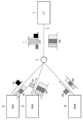
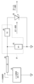
図1は、従来のPONシステムの概念を示す図である。PONシステムは、光ファイバ伝送路中に設置された光スプリッタ2を介して、収容局に設置された1台の終端装置(OLT:Optical Line Terminal)1に対して、複数の加入者宅に設置された宅内装置(ONU:Optical Network Unit)31-3Nを収容する。光ファイバ伝送路4、光スプリッタ2、およびOLT1を、複数の加入者間で共有する光アクセスシステムである。OLT1からONU31-3Nへの下り信号(DN0)は、時分割多重(TDM:Time Division Multiplexing)され、光スプリッタ2で分岐されて(DN1-DNN)各加入者に伝送される。ONU31-3Nからの上り信号(UP1-UPN)は、各加入者から時分割多元アクセス(TDMA:Time Division Multiple Access)により多重化されて(UP0)OLT1に伝送される。このとき、各ONUのからの上り信号の干渉を防ぐために、ガードタイムTを設定している。
FIG. 1 is a diagram showing the concept of a conventional PON system. The PON system accommodates one terminal device (OLT: Optical Line Terminal) 1 installed in a accommodating station, and home devices (ONU: Optical Network Unit) 3 1 -3 N installed in a plurality of subscribers' homes, via an
PONシステムは、ITU-Tにおいては、B-PON、G-PON、XG-PON、NG-PON2が標準化されており、IEEEにおいては、GE-PON、10GE-PONが標準化されている。それぞれ、1波長あたりの伝送レートは10Gbpsまで高速化されている。さらなるPONシステムの高速化、および高度化を目指し、次世代PONシステムの検討がされており、ITU-Tでは50G-PON、IEEEでは25G-EPONと呼ばれるシステムの議論が始まっている。これらのPONシステムでは、1波長あたりの伝送レートが従来の10Gbpsを超えた、25Gbps、50Gbpsにて検討されている。 ITU-T has standardized B-PON, G-PON, XG-PON, and NG-PON2 PON systems, while IEEE has standardized GE-PON and 10GE-PON. The transmission rate per wavelength has been increased to 10 Gbps for each system. Aiming to further increase the speed and sophistication of PON systems, next-generation PON systems are being studied, and discussions have begun on a system called 50G-PON in ITU-T and 25G-EPON in IEEE. These PON systems are being considered for transmission rates per wavelength of 25 Gbps and 50 Gbps, exceeding the conventional 10 Gbps.
このような高速な伝送レートを実現するためには、光送受信機の高速化が必要である。PONシステムにおいては、1台のOLTに複数台のONUを収容するため、各ONUから任意のタイミングで光信号を発生または消光する必要があり、それを実現するための光バースト送信機の高速化が欠かせない。また、高速化に伴い受信機での受信感度が劣化することから、10Gbps級のシステムと同様のバジェットを確保するために、光バースト送信機の高出力化も欠かせない。 To achieve such high transmission rates, optical transceivers need to be made faster. In a PON system, one OLT can accommodate multiple ONUs, so each ONU needs to be able to generate or turn off optical signals at any time, and to achieve this, high-speed optical burst transmitters are essential. In addition, as speeds increase, the receiving sensitivity of the receiver deteriorates, so in order to ensure a budget similar to that of a 10 Gbps-class system, it is also essential to increase the output of optical burst transmitters.
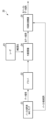
図2に、従来の光バースト送信機の構成を示す。光バースト送信機10は、バースト信号用MACチップ11、バースト信号用直接変調用レーザドライバ12、および直接変調用レーザ13が順に接続されている。バースト信号用MACチップ11からデータ信号およびバースト制御信号が出力される。このデータ信号およびバースト制御信号は、バースト信号用直接変調用レーザドライバ12に入力される。バースト信号用直接変調用レーザドライバ12に、バースト制御信号のON信号が入力されたとき、バースト信号用直接変調用レーザドライバ12はONとなりバーストデータ信号が出力される。このバーストデータ信号が直接変調用レーザ13に入力され、光バーストデータ信号が発生する。バースト信号用直接変調用レーザドライバ12に、バースト制御信号のOFF信号が入力されたとき、バースト信号用直接変調用レーザドライバはOFFとなりバーストデータ信号は出力されない。
Figure 2 shows the configuration of a conventional optical burst transmitter. In the
光バースト送信機の高速化には、これらのすべての部品の高速化が欠かせない。しかしながら、実用レベルの高速な直接変調レーザの速度は、高速化の研究がなされているが、現在25Gbps級レベルまでとなっている。また、直接変調用レーザを高速化するために、レーザの共振器長を短くする必要がある。これに伴って、出力光のパワーが低下するので、高速化と高出力化の両立が課題である。 Increasing the speed of optical burst transmitters requires increasing the speed of all of these components. However, while research is being conducted into increasing the speed of practical high-speed directly modulated lasers, the current speed is limited to around 25 Gbps. Furthermore, in order to increase the speed of directly modulated lasers, it is necessary to shorten the length of the laser cavity. As a result, the power of the output light decreases, so achieving both high speed and high output is a challenge.
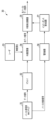
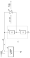
図3に、従来の外部変調器と半導体光増幅器を用いた光バースト送信機の構成を示す。上述した課題を解決する方法として、直接変調用レーザの代わりに外部変調器と半導体光増幅器を使用した方法がある(例えば、非特許文献参照)。光バースト送信機20は、外部変調器24によって高速化を、半導体光増幅器25によって高出力化を実現している。光バースト送信機20においては、バースト信号用MACチップ21から発生しているデータ信号は、ドライバ22を介して外部変調器24へ入力される。外部変調器24にはレーザ23から無変調の光信号も入力されており、外部変調器24から、変調された光データ信号が半導体光増幅器25へ入力される。バースト信号用MACチップ21から出力されているバースト制御信号は、半導体光増幅器25に入力され、バースト制御信号がONのとき半導体光増幅器25から光バーストデータ信号が出力され、バースト制御信号がOFFのとき半導体光増幅器25では光データ信号が消光され、光バーストデータ信号は出力されない。光バースト送信機20は、バースト信号専用のデバイスはMACチップのみとなっており、その他は、通常の連続信号用のデバイスを使用可能である.従って、光バースト送信機の低コストが可能である。
Figure 3 shows the configuration of a conventional optical burst transmitter using an external modulator and a semiconductor optical amplifier. As a method for solving the above-mentioned problem, there is a method of using an external modulator and a semiconductor optical amplifier instead of a direct modulation laser (for example, see non-patent literature). The
図4を参照して、従来の光バースト送信機の課題を説明する。バースト制御信号がONからOFFへ遷移するとき、光バーストデータ信号の立ち下りにおいて、数10nsec~数100nsの遅延dDNが生じる。同様に、バースト制御信号がOFFからONへ遷移するとき、光バーストデータ信号の立ち上がりにおいても遅延dUPが生じる。図1に示したように、各ONUからの上り信号を切り替える時の干渉を防ぐために、ガードタイムが設定されている。光バーストデータ信号の立ち下りの遅延および立ち上りの遅延が生じている場合、このガードタイムを長くとる必要があり、データ伝送が非効率となる。 The problems of the conventional optical burst transmitter will be described with reference to Fig. 4. When the burst control signal transitions from ON to OFF, a delay dDN of several tens of nanoseconds to several hundreds of nanoseconds occurs in the fall of the optical burst data signal. Similarly, when the burst control signal transitions from OFF to ON, a delay dUP also occurs in the rise of the optical burst data signal. As shown in Fig. 1, a guard time is set to prevent interference when switching the upstream signal from each ONU. When a delay occurs in the fall and rise of the optical burst data signal, this guard time must be long, which makes data transmission inefficient.
本発明の目的は、高効率な光バースト送信機を提供することにある。 The object of the present invention is to provide a highly efficient optical burst transmitter.
本発明は、このような目的を達成するために、一実施態様は、データ信号およびバースト制御信号を出力する制御回路と、データ信号により変調された光データ信号を、バースト制御信号により制御された光バーストデータ信号として出力する半導体光増幅器とを有する光バースト送信機において、制御回路と半導体光増幅器とを接続し、バースト制御信号を伝送する電気線路と、電気線路の特性インピーダンスと半導体光増幅器とをインピーダンス整合させるためのインピーダンス整合回路と、を備えたことを特徴とする光バースト送信機であって、インピーダンス整合回路は、電気線路の特性インピーダンスをZ0としたとき、半導体光増幅器と並列にZ0の抵抗値となることを特徴とする。 To achieve this object, one embodiment of the present invention is an optical burst transmitter having a control circuit that outputs a data signal and a burst control signal, and a semiconductor optical amplifier that outputs an optical data signal modulated by the data signal as an optical burst data signal controlled by a burst control signal, the optical burst transmitter comprising: an electrical line that connects the control circuit and the semiconductor optical amplifier and transmits the burst control signal; and an impedance matching circuit for impedance matching the characteristic impedance of the electrical line and the semiconductor optical amplifier, the impedance matching circuit being characterized in that when the characteristic impedance of the electrical line is Z0, the impedance matching circuit has a resistance value of Z0 in parallel with the semiconductor optical amplifier.
この構成によれば、光バーストデータ信号の立ち下りの遅延および立ち上りの遅延を抑制し、高効率な光バースト送信機を提供することができる。 This configuration makes it possible to suppress delays in the fall and rise of the optical burst data signal, providing a highly efficient optical burst transmitter.
以下、図面を参照しながら本発明の実施形態について詳細に説明する。 The following describes in detail an embodiment of the present invention with reference to the drawings.
[光バースト送信機]
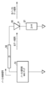
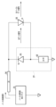
図5に、本発明の一実施形態にかかる光バースト送信機の構成を示す。光バースト送信機30は、データ信号およびバースト制御信号を出力する制御回路であるバースト信号用MAC(Media Access Control)チップ31と、データ信号を増幅するドライバ32と、レーザ33から無変調光が入力され、無変調光をデータ信号によって変調し光データ信号を出力する外部変調器34と、バースト制御信号に従い光データ信号を増幅ならびに消光する半導体光増幅器35とが順に接続されている。バースト制御信号を伝送する電気線路36は、インピーダンス整合するためのインピーダンス整合回路37を介して、バースト信号用MACチップ31と半導体光増幅器35とを接続している。
[Optical burst transmitter]
5 shows the configuration of an optical burst transmitter according to one embodiment of the present invention. The
レーザ33と外部変調器34とが一体的に集積された構成としてもよく、加えて半導体光増幅器35も一体的に集積してもよい。インピーダンス整合回路37は、半導体光増幅器と同一のパッケージに実装してもよい。
The
[第1の実施形態]
図6を参照して、第1の実施形態の光バースト送信機の動作を説明する。バースト信号用MACチップ31から出力されたバースト制御信号は、電気線路36を通じて半導体光増幅器35に入力される。バースト制御信号がOFFからONになったとき、半導体光増幅器35は、光データ信号を増幅する。このとき、バースト制御信号は、半導体光増幅器35に対して順方向の電流を入力することにより、光データ信号を増幅させる。
[First embodiment]
The operation of the optical burst transmitter of the first embodiment will be described with reference to Fig. 6. The burst control signal output from the burst
一般的に、高速のデータ信号を伝送する電気線路の特性インピーダンスは、50Ωに設定される。これに対して、半導体光増器35の順方向の抵抗は、数Ω程度(Rf)と非常に低い値である。そこで、バースト制御信号を伝送する電気線路36の特性インピーダンスZ0と半導体光増幅器35とをインピーダンス整合させるために、半導体光増幅器35と直列にZ0-Rfの抵抗値となるインピーダンス整合回路37を挿入する。このような構成により、バースト制御信号がOFFからONになったとき、光バーストデータ信号の立ち上りの遅延を抑制することが可能となる。
Typically, the characteristic impedance of an electrical line that transmits high-speed data signals is set to 50 Ω. In contrast, the forward resistance of the semiconductor
[第2の実施形態]
図7を参照して、第2の実施形態の光バースト送信機の動作を説明する。バースト信号用MACチップ31から出力されたバースト制御信号は、電気線路36を通じて半導体光増幅器35に入力される。バースト制御信号がONからOFFになったとき、光データ信号を半導体光増幅器35にて、消光する必要がある。このとき、バースト制御信号は、半導体光増幅器35に対して逆方向の電流を入力することにより、光データ信号を吸収させる。
Second Embodiment
The operation of the optical burst transmitter of the second embodiment will be described with reference to Fig. 7. The burst control signal output from the burst
半導体光増幅器の逆方向の抵抗分は、一般に大きな値を有しており、実効的に無限大と考えられる。そこで、電気線路36の特性インピーダンスZ0と半導体光増幅器35とをインピーダンス整合させるために、半導体光増幅器35と並列にZ0の抵抗値となるインピーダンス整合回路37を挿入する。このような構成により、バースト制御信号がONからOFFになったとき、光バーストデータ信号の立ち下りの遅延を抑制して消光することが可能となる。
The reverse resistance of a semiconductor optical amplifier generally has a large value and is effectively considered to be infinite. Therefore, in order to impedance match the characteristic impedance Z0 of the
[第3の実施形態]
第1の実施形態の光バースト送信機は、インピーダンス整合回路37である抵抗と半導体光増幅器35とが直列に並んでいるため、バースト制御信号がOFFからONになったとき、光バーストデータ信号の立ち上りの遅延を抑制することが可能となる。一方で、バースト制御信号がONからOFFになったとき、光バーストデータ信号は、立ち下りの遅延が発生する。
[Third embodiment]
In the optical burst transmitter of the first embodiment, since the resistor serving as the
第2の実施形態の光バースト送信機は、インピーダンス整合回路37である抵抗と半導体光増幅器35とが並列に並んでいるため、バースト制御信号がONからOFFになったとき、光バーストデータ信号は立ち下りの遅延を抑制することが可能となる。一方で、バースト制御信号がOFFからONになったとき、光バーストデータ信号は、立ち上りの遅延が発生する。従って、立ち上りの遅延と立ち下りの遅延の双方を抑制するためには、半導体光増幅器35に対して、直列と並列双方に抵抗分が挿入されたインピーダンス整合回路が必要となる。
In the optical burst transmitter of the second embodiment, the resistor that is the
図8を参照して、第3の実施形態の光バースト送信機の動作を説明する。バースト信号用MACチップ31から出力されたバースト制御信号は、電気線路36を通じて半導体光増幅器35に入力される。バースト制御信号がONからOFFとなったとき、光データ信号を半導体光増幅器35にて、消光する必要がある。このとき、バースト制御信号は、半導体光増幅器35に対して逆方向の電流を入力することにより、光データ信号を吸収させる。半導体光増幅器の逆方向の抵抗分は、一般に大きな値を有しており、実効的に無限大と考えられる。そこで、電気線路36の特性インピーダンスZ0と半導体光増幅器35とをインピーダンス整合させるために、半導体光増幅器35と並列にRP1の抵抗値となる抵抗P1を挿入する。
The operation of the optical burst transmitter of the third embodiment will be described with reference to FIG. 8. The burst control signal output from the burst
バースト制御信号がOFFからONとなったとき、半導体光増幅器35は、光データ信号を増幅する。このとき、バースト制御信号は、半導体光増幅器35に対して順方向の電流を入力することにより、光データ信号を増幅させる。半導体光増幅器35の順方向の抵抗は、数Ω程度(Rf)と非常に低い値である。そこで、バースト制御信号を伝送する電気線路36の特性インピーダンスZ0と半導体光増幅器35とをインピーダンス整合させるために、半導体光増幅器35と直列にRS1の抵抗値となる抵抗S1を挿入する。このように、第3の実施形態のインピーダンス整合回路37は、抵抗P1と抵抗S1とから構成される。
When the burst control signal changes from OFF to ON, the semiconductor
バースト制御信号がOFFからONになったときのインピーダンス整合回路37と半導体光増幅器35とを合わせたインピーダンスZonは、
The impedance Zon of the

となる。バースト制御信号がONからOFFになったときのインピーダンス整合回路37と半導体光増幅器35を合わせたインピーダンスZoffは、RP1となる。
The combined impedance Zoff of the
バースト制御信号がOFFからONになったときのインピーダンスZonと、バースト制御信号がONからOFFになったときのインピーダンスZoffとが一致するためには、 In order for the impedance Zon when the burst control signal changes from OFF to ON to match the impedance Zoff when the burst control signal changes from ON to OFF,

となる必要があるが、これを満たすRS1とRP1の抵抗値はない。そのため、ZonとZoffはどちらか一方を電気線路の特性インピーダンスZ0と一致する値とし、立ち上りまたは立ち下りの一方の遅延を抑制し、他方の遅延は許容される値となるようにする。 However, there are no resistance values for RS1 and RP1 that satisfy this. Therefore, one of Zon and Zoff is set to a value that matches the characteristic impedance Z0 of the electrical line, suppressing the delay in either the rising or falling edge, while setting the other delay to an acceptable value.
抵抗S1,P1の値を、 The values of resistors S1 and P1 are

となるように設定した場合、バースト制御信号がOFFからONになったときのインピーダンス整合回路37と半導体光増幅器35とを合わせたインピーダンスZonが電気回路36の特性インピーダンスZ0と一致する。このことから、光バーストデータ信号の立ち上りの遅延を抑制することが可能となる。
When set as above, the combined impedance Zon of the
また、抵抗P1の値をRP1=Z0となるように設定した場合、バースト制御信号がONからOFFになったときのインピーダンス整合回路37と半導体光増幅器35とを合わせたインピーダンスZoffが電気回路36の特性インピーダンスZ0と一致する。このことから、光バーストデータ信号の立ち下りの遅延を抑制して消光することが可能となる。
In addition, if the value of resistor P1 is set so that RP1 = Z0, the combined impedance Zoff of the
[第4の実施形態]
第1の実施形態の光バースト送信機は、インピーダンス整合回路37である抵抗と半導体光増幅器35とが直列に並んでいるため、バースト制御信号がOFFからONになったとき、光バーストデータ信号の立ち上りの遅延を抑制することが可能となる。一方で、バースト制御信号がONからOFFになったとき、光バーストデータ信号は、立ち下りの遅延が発生する。
[Fourth embodiment]
In the optical burst transmitter of the first embodiment, since the resistor serving as the
第2の実施形態の光バースト送信機は、インピーダンス整合回路37である抵抗と半導体光増幅器35とが並列に並んでいるため、バースト制御信号がONからOFFになったとき、光バーストデータ信号は立ち下りの遅延を抑制することが可能となる。一方で、バースト制御信号がOFFからONになったとき、光バーストデータ信号は、立ち上りの遅延が発生する。従って、立ち上りの遅延と立ち下りの遅延の双方を抑制するためには、半導体光増幅器35に対し、直列と並列双方に抵抗分が挿入されたインピーダンス整合回路が必要となる。
In the optical burst transmitter of the second embodiment, the resistor that is the
図9を参照して、第4の実施形態の光バースト送信機の動作を説明する。バースト信号用MACチップ31から出力されたバースト制御信号は、電気線路36を通じて半導体光増幅器35に入力される。バースト制御信号がONからOFFとなったとき、光データ信号を半導体光増幅器35にて、消光する必要がある。このとき、バースト制御信号は、半導体光増幅器35に対して逆方向の電流を入力することにより、光データ信号を吸収させる。半導体光増幅器の逆方向の抵抗分は、一般に大きな値を有しており、実効的に無限大と考えられる。そこで、電気線路36の特性インピーダンスZ0と半導体光増幅器35とをインピーダンス整合させるために、半導体光増幅器35と並列にRP2の抵抗値となる抵抗P2を挿入する。
The operation of the optical burst transmitter of the fourth embodiment will be described with reference to FIG. 9. The burst control signal output from the
バースト制御信号がOFFからONとなったとき、半導体光増幅器35は、光データ信号を増幅する。このとき、バースト制御信号は、半導体光増幅器35に対して順方向の電流を入力することにより、光データ信号を増幅させる。半導体光増幅器35の順方向の抵抗は、数Ω程度(Rf)と非常に低い値である。そこで、バースト制御信号を伝送する電気線路36の特性インピーダンスZ0と半導体光増幅器35とをインピーダンス整合させるために、半導体光増幅器35と抵抗P2からなる並列回路と直列にRS2の抵抗値となる抵抗S2を挿入する。このように、第4の実施形態のインピーダンス整合回路37は、抵抗P2と抵抗S2とから構成される。
When the burst control signal changes from OFF to ON, the semiconductor
抵抗P2と抵抗S2の抵抗値は、電気線路36の特性インピーダンスZ0と整合するようにする必要がある。バースト制御信号がOFFからONになったときのインピーダンス整合回路37と半導体光増幅器35とを合わせたインピーダンスZonは、
The resistance values of resistors P2 and S2 must be matched with the characteristic impedance Z0 of the

となる。バースト制御信号がONからOFFになったときのインピーダンス整合回路37と半導体光増幅器35を合わせたインピーダンスZoffは、RS2+RP2となる。
The impedance Zoff of the
バースト制御信号がOFFからONになったときのインピーダンスZonと、バースト制御信号がONからOFFになったときのインピーダンスZoffとが一致するためには、 In order for the impedance Zon when the burst control signal changes from OFF to ON to match the impedance Zoff when the burst control signal changes from ON to OFF,

となる必要があるが、これを満たすRS1とRP1の抵抗値はない。そのため、ZonとZoffは、電気線路36の特性インピーダンスZ0とおおよそ一致する値にする必要がある。このとき、高周波回路では、反射減衰量RLが20dB以上であることが一つの指標となる。反射減衰量は、特性インピーダンスをZ0、入力インピーダンスをZLとしたとき、
However, there are no resistance values for RS1 and RP1 that satisfy this. Therefore, Zon and Zoff must be set to values that roughly match the characteristic impedance Z0 of the

と表現される。ZLの範囲は、0.82×Z0<ZL<1.22×Z0となり、以下の式(1)と式(2)を境界線とする範囲で表現することできる。 The range of ZL is 0.82 x Z0 < ZL < 1.22 x Z0, and can be expressed as a range with the boundaries being the following equations (1) and (2).

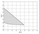
図10に、第4の実施形態のインピーダンス整合回路の抵抗値の範囲を示す。Rf=5Ω、Z0=50Ωのとき、式(1)と式(2)を満たす範囲を図示している。任意のRfに応じて式(1)、式(2)を満たす、RP2,RS2の値を選択することにより、反射減衰量20dB以上を有し、電気線路36の特性インピーダンスZ0にほぼ整合したインピーダンス整合回路37を構成することが可能となる。このことから、バースト制御信号がONからOFFになったとき、バースト制御信号がOFFからONになったときの双方で、光バーストデータ信号の立ち下りの遅延と立ち上りの遅延とを、ほぼ抑制することが可能となる。
Figure 10 shows the range of resistance values of the impedance matching circuit of the fourth embodiment. The figure shows the range that satisfies formulas (1) and (2) when Rf = 5Ω and Z0 = 50Ω. By selecting values of RP2 and RS2 that satisfy formulas (1) and (2) according to an arbitrary Rf, it is possible to configure an
[第5の実施形態]
図11を参照して、第5の実施形態の光バースト送信機の動作を説明する。バースト信号用MACチップ31から出力されたバースト制御信号は、電気線路36を通じて半導体光増幅器35に入力される。第5の実施形態のインピーダンス整合回路37は、第4の実施形態のインピーダンス整合回路37の抵抗P2を、ダイオードD1に置き換えた構成とする。ダイオードD1は、半導体光増幅器35と並列に逆向きに挿入される。ダイオードD1は、順方向および逆方向の抵抗分が、半導体光増幅器35の抵抗値と同一である。インピーダンス整合回路37は、半導体光増幅器35とダイオードD1からなる並列回路と直列にZ0-Rfの抵抗値となる抵抗S3が挿入されている。
[Fifth embodiment]
The operation of the optical burst transmitter of the fifth embodiment will be described with reference to Fig. 11. A burst control signal output from the burst
バースト制御信号がOFFからONとなったとき、半導体光増幅器35は、光データ信号を増幅する。このとき、バースト制御信号は、半導体光増幅器35に対して順方向の電流を入力することにより、光データ信号を増幅させる。半導体光増幅器35の順方向の抵抗は、数Ω程度(Rf)と非常に低い値である。一方、インピーダンス整合回路37のダイオードD1の逆方向の抵抗は、実効的に無限大と考えられる。そこで、バースト制御信号を伝送する電気線路36の特性インピーダンスZ0と半導体光増幅器35とをインピーダンス整合させるために、半導体光増幅器35と直列にZ0-Rfの抵抗値となる抵抗S3を挿入する。このような構成により、バースト制御信号がOFFからONになったとき、光バーストデータ信号の立ち上りの遅延を抑制することが可能となる。
When the burst control signal changes from OFF to ON, the semiconductor
バースト制御信号がONからOFFとなったとき、光データ信号を半導体光増幅器35にて、消光する必要がある。このとき、バースト制御信号は、半導体光増幅器35に対して逆方向の電流を入力することにより、光データ信号を吸収させる。半導体光増幅器35の逆方向の抵抗分は、一般に大きな値を有しており、実効的に無限大と考えられる。一方、インピーダンス整合回路37のダイオードD1の順方向の抵抗Rdは、数Ω程度である。そこで、電気線路36の特性インピーダンスZ0と半導体光増幅器35とをインピーダンス整合させるために、半導体光増幅器35と並列に逆向きにダイオードD1を挿入している。このような構成により、バースト制御信号がONからOFFになったとき、光バーストデータ信号の立ち下りの遅延を抑制して消光することが可能となる。
When the burst control signal changes from ON to OFF, the optical data signal needs to be extinguished by the semiconductor
[第6の実施形態]
図12を参照して、第6の実施形態の光バースト送信機の動作を説明する。バースト信号用MACチップ31から出力されたバースト制御信号は、電気線路36を通じて半導体光増幅器35に入力される。第6の実施形態のインピーダンス整合回路37は、半導体光増幅器35と直列にZ0-Rfの抵抗値となる抵抗S4と、半導体光増幅器35と並列に逆向きに挿入されたダイオードD2および抵抗値Z0-Rfとなる抵抗S5からなる直列回路とを含む。ダイオードD2は、順方向および逆方向の抵抗分が、半導体光増幅器35の抵抗値と同一である。
Sixth embodiment
The operation of the optical burst transmitter of the sixth embodiment will be described with reference to Fig. 12. The burst control signal output from the burst
バースト制御信号がOFFからONとなったとき、半導体光増幅器35は、光データ信号を増幅する。このとき、バースト制御信号は、半導体光増幅器35に対して順方向の電流を入力することにより、光データ信号を増幅させる。半導体光増幅器35の順方向の抵抗は、数Ω程度(Rf)と非常に低い値である。一方、インピーダンス整合回路37のダイオードD2の逆方向の抵抗は、実効的に無限大と考えられる。そこで、バースト制御信号を伝送する電気線路36の特性インピーダンスZ0と半導体光増幅器35とをインピーダンス整合させるために、半導体光増幅器35と直列にZ0-Rfの抵抗値となる抵抗S4を挿入する。このような構成により、バースト制御信号がOFFからONになったとき、光バーストデータ信号の立ち上りの遅延を抑制することが可能となる。
When the burst control signal changes from OFF to ON, the semiconductor
バースト制御信号がONからOFFとなったとき、光データ信号を半導体光増幅器35にて、消光する必要がある。このとき、バースト制御信号は、半導体光増幅器35に対して逆方向の電流を入力することにより、光データ信号を吸収させる。半導体光増幅器35の逆方向の抵抗分は、一般に大きな値を有しており、実効的に無限大と考えられる。一方、インピーダンス整合回路37のダイオードD2の順方向の抵抗Rdは、数Ω程度である。そこで、電気線路36の特性インピーダンスZ0とインピーダンス整合するために、半導体光増幅器35と並列に逆向きにダイオードD2を挿入している。このような構成により、バースト制御信号がONからOFFになったとき、光バーストデータ信号の立ち下りの遅延を抑制して消光することが可能となる。
When the burst control signal changes from ON to OFF, the optical data signal needs to be extinguished by the semiconductor
本発明は、光バースト送信機に適用することができる。 The present invention can be applied to optical burst transmitters.
Claims (6)
前記制御回路と前記半導体光増幅器とを接続し、前記バースト制御信号を伝送する電気線路と、
前記電気線路の特性インピーダンスと前記半導体光増幅器とをインピーダンス整合させるためのインピーダンス整合回路と
を備え、
前記インピーダンス整合回路は、前記電気線路の特性インピーダンスをZ0としたとき、前記半導体光増幅器と並列にZ0の抵抗値となることを特徴とする光バースト送信機。 An optical burst transmitter having a control circuit which outputs a data signal and a burst control signal, and a semiconductor optical amplifier which outputs an optical data signal modulated by the data signal as an optical burst data signal controlled by the burst control signal,
an electric line connecting the control circuit and the semiconductor optical amplifier and transmitting the burst control signal;
an impedance matching circuit for matching a characteristic impedance of the electric line with the semiconductor optical amplifier,
11. An optical burst transmitter, comprising: said impedance matching circuit, when a characteristic impedance of said electric line is Z0, and which is connected in parallel with said semiconductor optical amplifier has a resistance value of Z0.
前記制御回路と前記半導体光増幅器とを接続し、前記バースト制御信号を伝送する電気線路と、
前記電気線路の特性インピーダンスと前記半導体光増幅器とをインピーダンス整合させるためのインピーダンス整合回路と
を備え、
前記インピーダンス整合回路は、前記半導体光増幅器の順方向の抵抗値をRf、前記電気線路の特性インピーダンスをZ0としたとき、前記半導体光増幅器と並列にRP1の抵抗値となる第1抵抗と、前記半導体光増幅器と直列にRS1の抵抗値となる第2抵抗とを含み、

an electric line connecting the control circuit and the semiconductor optical amplifier and transmitting the burst control signal;
an impedance matching circuit for matching a characteristic impedance of the electric line with the semiconductor optical amplifier,
the impedance matching circuit includes a first resistor in parallel with the semiconductor optical amplifier and having a resistance value of RP1, and a second resistor in series with the semiconductor optical amplifier and having a resistance value of RS1, where Rf is a forward resistance value of the semiconductor optical amplifier and Z0 is a characteristic impedance of the electric line;
前記制御回路と前記半導体光増幅器とを接続し、前記バースト制御信号を伝送する電気線路と、
前記電気線路の特性インピーダンスと前記半導体光増幅器とをインピーダンス整合させるためのインピーダンス整合回路と
を備え、
前記インピーダンス整合回路は、前記半導体光増幅器の順方向の抵抗値をRf、前記電気線路の特性インピーダンスをZ0としたとき、前記半導体光増幅器と並列にRP1の抵抗値となる第1抵抗と、前記半導体光増幅器と直列にRS1の抵抗値となる第2抵抗とを含み、RP1=Z0となるように設定されていることを特徴とする光バースト送信機。 An optical burst transmitter having a control circuit which outputs a data signal and a burst control signal, and a semiconductor optical amplifier which outputs an optical data signal modulated by the data signal as an optical burst data signal controlled by the burst control signal,
an electric line connecting the control circuit and the semiconductor optical amplifier and transmitting the burst control signal;
an impedance matching circuit for matching a characteristic impedance of the electric line with the semiconductor optical amplifier,
The impedance matching circuit includes a first resistor in parallel with the semiconductor optical amplifier and having a resistance value of RP1, and a second resistor in series with the semiconductor optical amplifier and having a resistance value of RS1, where Rf is the forward resistance value of the semiconductor optical amplifier and Z0 is the characteristic impedance of the electrical line, and the impedance matching circuit is set so that RP1=Z0.
前記制御回路と前記半導体光増幅器とを接続し、前記バースト制御信号を伝送する電気線路と、
前記電気線路の特性インピーダンスと前記半導体光増幅器とをインピーダンス整合させるためのインピーダンス整合回路と
を備え、
前記インピーダンス整合回路は、前記半導体光増幅器の順方向の抵抗値をRf、前記電気線路の特性インピーダンスをZ0としたとき、前記半導体光増幅器と並列にRP2の抵抗値となる第1抵抗と、前記半導体光増幅器と前記第1抵抗とからなる並列回路と直列にRS2の抵抗値となる第2抵抗とを含み、

an electric line connecting the control circuit and the semiconductor optical amplifier and transmitting the burst control signal;
an impedance matching circuit for matching a characteristic impedance of the electric line with the semiconductor optical amplifier,
the impedance matching circuit includes a first resistor having a resistance value of RP2 in parallel with the semiconductor optical amplifier, and a second resistor having a resistance value of RS2 in series with a parallel circuit made of the semiconductor optical amplifier and the first resistor, where Rf is a forward resistance value of the semiconductor optical amplifier and Z0 is a characteristic impedance of the electric line;
前記制御回路と前記半導体光増幅器とを接続し、前記バースト制御信号を伝送する電気線路と、
前記電気線路の特性インピーダンスと前記半導体光増幅器とをインピーダンス整合させるためのインピーダンス整合回路と
を備え、
前記インピーダンス整合回路は、前記半導体光増幅器の順方向の抵抗値をRf、前記電気線路の特性インピーダンスをZ0としたとき、前記半導体光増幅器と並列に逆向き挿入されたダイオードと、前記半導体光増幅器と前記ダイオードとからなる並列回路と直列にZ0-Rfの抵抗値となる抵抗とを含み、前記ダイオードは、順方向および逆方向の抵抗分が前記半導体光増幅器の抵抗値と同一であることを特徴とする光バースト送信機。 An optical burst transmitter having a control circuit which outputs a data signal and a burst control signal, and a semiconductor optical amplifier which outputs an optical data signal modulated by the data signal as an optical burst data signal controlled by the burst control signal,
an electric line connecting the control circuit and the semiconductor optical amplifier and transmitting the burst control signal;
an impedance matching circuit for matching a characteristic impedance of the electric line with the semiconductor optical amplifier,
The impedance matching circuit includes a diode inserted in reverse in parallel with the semiconductor optical amplifier, and a resistor having a resistance value of Z0-Rf in series with a parallel circuit consisting of the semiconductor optical amplifier and the diode, where Rf is the forward resistance value of the semiconductor optical amplifier and Z0 is the characteristic impedance of the electrical line, and the forward and reverse resistance components of the diode are the same as the resistance value of the semiconductor optical amplifier.
前記制御回路と前記半導体光増幅器とを接続し、前記バースト制御信号を伝送する電気線路と、
前記電気線路の特性インピーダンスと前記半導体光増幅器とをインピーダンス整合させるためのインピーダンス整合回路と
を備え、
前記インピーダンス整合回路は、前記半導体光増幅器の順方向の抵抗値をRf、前記電気線路の特性インピーダンスをZ0としたとき、前記半導体光増幅器と直列にZ0-Rfの抵抗値となる第1抵抗と、前記半導体光増幅器と並列に逆向き挿入されたダイオードおよびZ0-Rfの抵抗値となる第2抵抗からなる直列回路とを含み、前記ダイオードは、順方向および逆方向の抵抗分が前記半導体光増幅器の抵抗値と同一であることを特徴とする光バースト送信機。 An optical burst transmitter having a control circuit which outputs a data signal and a burst control signal, and a semiconductor optical amplifier which outputs an optical data signal modulated by the data signal as an optical burst data signal controlled by the burst control signal,
an electric line connecting the control circuit and the semiconductor optical amplifier and transmitting the burst control signal;
an impedance matching circuit for matching a characteristic impedance of the electric line with the semiconductor optical amplifier,
The impedance matching circuit includes a first resistor having a resistance value of Z0-Rf in series with the semiconductor optical amplifier, and a series circuit including a diode inserted in reverse in parallel with the semiconductor optical amplifier and a second resistor having a resistance value of Z0-Rf, where Rf is the forward resistance value of the semiconductor optical amplifier and Z0 is the characteristic impedance of the electrical line, and the diode has forward and reverse resistance values equal to the resistance value of the semiconductor optical amplifier.
Priority Applications (1)
| Application Number | Priority Date | Filing Date | Title |
|---|---|---|---|
| JP2024158566A JP7783519B2 (en) | 2020-09-08 | 2024-09-12 | Optical Burst Transmitter |
Applications Claiming Priority (3)
| Application Number | Priority Date | Filing Date | Title |
|---|---|---|---|
| JP2022548279A JPWO2022054147A1 (en) | 2020-09-08 | 2020-09-08 | |
| PCT/JP2020/034014 WO2022054147A1 (en) | 2020-09-08 | 2020-09-08 | Optical burst transmitter |
| JP2024158566A JP7783519B2 (en) | 2020-09-08 | 2024-09-12 | Optical Burst Transmitter |
Related Parent Applications (1)
| Application Number | Title | Priority Date | Filing Date |
|---|---|---|---|
| JP2022548279A Division JPWO2022054147A1 (en) | 2020-09-08 | 2020-09-08 |
Publications (2)
| Publication Number | Publication Date |
|---|---|
| JP2024166328A true JP2024166328A (en) | 2024-11-28 |
| JP7783519B2 JP7783519B2 (en) | 2025-12-10 |
Family
ID=80630423
Family Applications (2)
| Application Number | Title | Priority Date | Filing Date |
|---|---|---|---|
| JP2022548279A Pending JPWO2022054147A1 (en) | 2020-09-08 | 2020-09-08 | |
| JP2024158566A Active JP7783519B2 (en) | 2020-09-08 | 2024-09-12 | Optical Burst Transmitter |
Family Applications Before (1)
| Application Number | Title | Priority Date | Filing Date |
|---|---|---|---|
| JP2022548279A Pending JPWO2022054147A1 (en) | 2020-09-08 | 2020-09-08 |
Country Status (3)
| Country | Link |
|---|---|
| US (1) | US12425105B2 (en) |
| JP (2) | JPWO2022054147A1 (en) |
| WO (1) | WO2022054147A1 (en) |
Citations (5)
| Publication number | Priority date | Publication date | Assignee | Title |
|---|---|---|---|---|
| JPH09307169A (en) * | 1996-05-20 | 1997-11-28 | Matsushita Electric Ind Co Ltd | Semiconductor laser module |
| JPH1098451A (en) * | 1996-09-24 | 1998-04-14 | Matsushita Electric Ind Co Ltd | Semiconductor laser module with multiple input terminals |
| JP2003023208A (en) * | 2001-07-05 | 2003-01-24 | Nec Corp | Variable wavelength semiconductor laser |
| JP2008084891A (en) * | 2006-09-25 | 2008-04-10 | Fujitsu Ltd | Optical semiconductor device and manufacturing method thereof |
| JP2012108210A (en) * | 2010-11-15 | 2012-06-07 | Fujitsu Ltd | Optical switch drive circuit, optical switch and optical change-over switch |
Family Cites Families (6)
| Publication number | Priority date | Publication date | Assignee | Title |
|---|---|---|---|---|
| JPH10173448A (en) * | 1996-12-13 | 1998-06-26 | Nec Miyagi Ltd | Semiconductor amplifier |
| JP3799874B2 (en) * | 1999-06-15 | 2006-07-19 | Kddi株式会社 | Polarization mode dispersion compensator |
| JP4199901B2 (en) * | 2000-03-10 | 2008-12-24 | 日本オプネクスト株式会社 | Optical transmission module |
| JP4957315B2 (en) * | 2007-03-26 | 2012-06-20 | 富士通株式会社 | Semiconductor optical amplification module, matrix optical switch device, and drive circuit |
| JP2018170705A (en) * | 2017-03-30 | 2018-11-01 | 住友電気工業株式会社 | Drive circuit |
| US10887021B2 (en) * | 2019-01-04 | 2021-01-05 | Calix, Inc. | Burst mode spectral excursion mitigation |
-
2020
- 2020-09-08 WO PCT/JP2020/034014 patent/WO2022054147A1/en not_active Ceased
- 2020-09-08 JP JP2022548279A patent/JPWO2022054147A1/ja active Pending
- 2020-09-08 US US18/043,925 patent/US12425105B2/en active Active
-
2024
- 2024-09-12 JP JP2024158566A patent/JP7783519B2/en active Active
Patent Citations (5)
| Publication number | Priority date | Publication date | Assignee | Title |
|---|---|---|---|---|
| JPH09307169A (en) * | 1996-05-20 | 1997-11-28 | Matsushita Electric Ind Co Ltd | Semiconductor laser module |
| JPH1098451A (en) * | 1996-09-24 | 1998-04-14 | Matsushita Electric Ind Co Ltd | Semiconductor laser module with multiple input terminals |
| JP2003023208A (en) * | 2001-07-05 | 2003-01-24 | Nec Corp | Variable wavelength semiconductor laser |
| JP2008084891A (en) * | 2006-09-25 | 2008-04-10 | Fujitsu Ltd | Optical semiconductor device and manufacturing method thereof |
| JP2012108210A (en) * | 2010-11-15 | 2012-06-07 | Fujitsu Ltd | Optical switch drive circuit, optical switch and optical change-over switch |
Non-Patent Citations (1)
| Title |
|---|
| TAGUCHI, K. ET AL.: "High Output Power and Burst Extinction Ratio ONU Using a Simple Configuration Booster SOA with Gain", OFC 2014, JPN6021004004, 2014, US, ISSN: 0005718378 * |
Also Published As
| Publication number | Publication date |
|---|---|
| US12425105B2 (en) | 2025-09-23 |
| JPWO2022054147A1 (en) | 2022-03-17 |
| US20230327775A1 (en) | 2023-10-12 |
| WO2022054147A1 (en) | 2022-03-17 |
| JP7783519B2 (en) | 2025-12-10 |
Similar Documents
| Publication | Publication Date | Title |
|---|---|---|
| JP5941150B2 (en) | Configuration for coexisting GPON and XGPON optical communication systems | |
| US8571410B2 (en) | Mutual wavelength locking in WDM-PONS | |
| EP1980039A1 (en) | Passive optical network comprising multi-longitudinal mode emitting devices | |
| US9236949B1 (en) | Laser transceiver with improved bit error rate | |
| CN104901744B (en) | The power equalizer of power equalization and this OLT are carried out to upward signal in the olt | |
| KR100906399B1 (en) | Method and system for controlling drive current of WMD-POON optical transmitter | |
| CN111478732A (en) | Optical line controller system for controlling passive optical network | |
| CN114402627B (en) | Port replicator | |
| CN112166535B (en) | Wavelength drift suppression for burst-mode tunable EML transmitters | |
| US20150381305A1 (en) | Self-calibrating tunable laser for optical network | |
| JP7783519B2 (en) | Optical Burst Transmitter | |
| CN102067485B (en) | Transmitter disabling device | |
| US8139955B2 (en) | Method and system for controlling driving current of WDM-PON optical transmitter | |
| US10299021B2 (en) | Optical signal amplification | |
| KR102280109B1 (en) | Passive optical network transceiver with multiple wavelength switching function and wavelength switching method thereof | |
| KR100840389B1 (en) | Hybrid Mode Optical Transmitter with Single Light Source | |
| Chang et al. | 1.25 Gb/s Uplink Burst–mode Transmissions: System Requirements and Optical Diagnostic Challenges of EPON Physical-layer Chipset for Enabling Broadband Optical Ethernet Access Networks | |
| WO2006069172A2 (en) | System and method for operating a wideband return channel in a bi-directional optical communication system |
Legal Events
| Date | Code | Title | Description |
|---|---|---|---|
| A621 | Written request for application examination |
Free format text: JAPANESE INTERMEDIATE CODE: A621 Effective date: 20240912 |
|
| TRDD | Decision of grant or rejection written | ||
| A01 | Written decision to grant a patent or to grant a registration (utility model) |
Free format text: JAPANESE INTERMEDIATE CODE: A01 Effective date: 20251028 |
|
| A61 | First payment of annual fees (during grant procedure) |
Free format text: JAPANESE INTERMEDIATE CODE: A61 Effective date: 20251110 |
|
| R150 | Certificate of patent or registration of utility model |
Ref document number: 7783519 Country of ref document: JP Free format text: JAPANESE INTERMEDIATE CODE: R150 |