JP2023166329A - Laminated electronic components - Google Patents
Laminated electronic components Download PDFInfo
- Publication number
- JP2023166329A JP2023166329A JP2023066023A JP2023066023A JP2023166329A JP 2023166329 A JP2023166329 A JP 2023166329A JP 2023066023 A JP2023066023 A JP 2023066023A JP 2023066023 A JP2023066023 A JP 2023066023A JP 2023166329 A JP2023166329 A JP 2023166329A
- Authority
- JP
- Japan
- Prior art keywords
- region
- core
- interface shell
- dielectric
- electronic component
- Prior art date
- Legal status (The legal status is an assumption and is not a legal conclusion. Google has not performed a legal analysis and makes no representation as to the accuracy of the status listed.)
- Pending
Links
Images

Classifications
-
- H—ELECTRICITY
- H01—ELECTRIC ELEMENTS
- H01G—CAPACITORS; CAPACITORS, RECTIFIERS, DETECTORS, SWITCHING DEVICES, LIGHT-SENSITIVE OR TEMPERATURE-SENSITIVE DEVICES OF THE ELECTROLYTIC TYPE
- H01G4/00—Fixed capacitors; Processes of their manufacture
- H01G4/30—Stacked capacitors
-
- H—ELECTRICITY
- H01—ELECTRIC ELEMENTS
- H01G—CAPACITORS; CAPACITORS, RECTIFIERS, DETECTORS, SWITCHING DEVICES, LIGHT-SENSITIVE OR TEMPERATURE-SENSITIVE DEVICES OF THE ELECTROLYTIC TYPE
- H01G4/00—Fixed capacitors; Processes of their manufacture
- H01G4/002—Details
- H01G4/018—Dielectrics
- H01G4/06—Solid dielectrics
- H01G4/08—Inorganic dielectrics
- H01G4/12—Ceramic dielectrics
- H01G4/1209—Ceramic dielectrics characterised by the ceramic dielectric material
- H01G4/1218—Ceramic dielectrics characterised by the ceramic dielectric material based on titanium oxides or titanates
-
- C—CHEMISTRY; METALLURGY
- C04—CEMENTS; CONCRETE; ARTIFICIAL STONE; CERAMICS; REFRACTORIES
- C04B—LIME, MAGNESIA; SLAG; CEMENTS; COMPOSITIONS THEREOF, e.g. MORTARS, CONCRETE OR LIKE BUILDING MATERIALS; ARTIFICIAL STONE; CERAMICS; REFRACTORIES; TREATMENT OF NATURAL STONE
- C04B35/00—Shaped ceramic products characterised by their composition; Ceramics compositions; Processing powders of inorganic compounds preparatory to the manufacturing of ceramic products
- C04B35/01—Shaped ceramic products characterised by their composition; Ceramics compositions; Processing powders of inorganic compounds preparatory to the manufacturing of ceramic products based on oxide ceramics
- C04B35/46—Shaped ceramic products characterised by their composition; Ceramics compositions; Processing powders of inorganic compounds preparatory to the manufacturing of ceramic products based on oxide ceramics based on titanium oxides or titanates
- C04B35/462—Shaped ceramic products characterised by their composition; Ceramics compositions; Processing powders of inorganic compounds preparatory to the manufacturing of ceramic products based on oxide ceramics based on titanium oxides or titanates based on titanates
- C04B35/465—Shaped ceramic products characterised by their composition; Ceramics compositions; Processing powders of inorganic compounds preparatory to the manufacturing of ceramic products based on oxide ceramics based on titanium oxides or titanates based on titanates based on alkaline earth metal titanates
- C04B35/468—Shaped ceramic products characterised by their composition; Ceramics compositions; Processing powders of inorganic compounds preparatory to the manufacturing of ceramic products based on oxide ceramics based on titanium oxides or titanates based on titanates based on alkaline earth metal titanates based on barium titanates
- C04B35/4682—Shaped ceramic products characterised by their composition; Ceramics compositions; Processing powders of inorganic compounds preparatory to the manufacturing of ceramic products based on oxide ceramics based on titanium oxides or titanates based on titanates based on alkaline earth metal titanates based on barium titanates based on BaTiO3 perovskite phase
-
- C—CHEMISTRY; METALLURGY
- C04—CEMENTS; CONCRETE; ARTIFICIAL STONE; CERAMICS; REFRACTORIES
- C04B—LIME, MAGNESIA; SLAG; CEMENTS; COMPOSITIONS THEREOF, e.g. MORTARS, CONCRETE OR LIKE BUILDING MATERIALS; ARTIFICIAL STONE; CERAMICS; REFRACTORIES; TREATMENT OF NATURAL STONE
- C04B35/00—Shaped ceramic products characterised by their composition; Ceramics compositions; Processing powders of inorganic compounds preparatory to the manufacturing of ceramic products
- C04B35/01—Shaped ceramic products characterised by their composition; Ceramics compositions; Processing powders of inorganic compounds preparatory to the manufacturing of ceramic products based on oxide ceramics
- C04B35/48—Shaped ceramic products characterised by their composition; Ceramics compositions; Processing powders of inorganic compounds preparatory to the manufacturing of ceramic products based on oxide ceramics based on zirconium or hafnium oxides, zirconates, zircon or hafnates
- C04B35/49—Shaped ceramic products characterised by their composition; Ceramics compositions; Processing powders of inorganic compounds preparatory to the manufacturing of ceramic products based on oxide ceramics based on zirconium or hafnium oxides, zirconates, zircon or hafnates containing also titanium oxides or titanates
-
- C—CHEMISTRY; METALLURGY
- C04—CEMENTS; CONCRETE; ARTIFICIAL STONE; CERAMICS; REFRACTORIES
- C04B—LIME, MAGNESIA; SLAG; CEMENTS; COMPOSITIONS THEREOF, e.g. MORTARS, CONCRETE OR LIKE BUILDING MATERIALS; ARTIFICIAL STONE; CERAMICS; REFRACTORIES; TREATMENT OF NATURAL STONE
- C04B35/00—Shaped ceramic products characterised by their composition; Ceramics compositions; Processing powders of inorganic compounds preparatory to the manufacturing of ceramic products
- C04B35/622—Forming processes; Processing powders of inorganic compounds preparatory to the manufacturing of ceramic products
- C04B35/626—Preparing or treating the powders individually or as batches ; preparing or treating macroscopic reinforcing agents for ceramic products, e.g. fibres; mechanical aspects section B
- C04B35/628—Coating the powders or the macroscopic reinforcing agents
- C04B35/62802—Powder coating materials
- C04B35/62842—Metals
-
- C—CHEMISTRY; METALLURGY
- C04—CEMENTS; CONCRETE; ARTIFICIAL STONE; CERAMICS; REFRACTORIES
- C04B—LIME, MAGNESIA; SLAG; CEMENTS; COMPOSITIONS THEREOF, e.g. MORTARS, CONCRETE OR LIKE BUILDING MATERIALS; ARTIFICIAL STONE; CERAMICS; REFRACTORIES; TREATMENT OF NATURAL STONE
- C04B35/00—Shaped ceramic products characterised by their composition; Ceramics compositions; Processing powders of inorganic compounds preparatory to the manufacturing of ceramic products
- C04B35/622—Forming processes; Processing powders of inorganic compounds preparatory to the manufacturing of ceramic products
- C04B35/626—Preparing or treating the powders individually or as batches ; preparing or treating macroscopic reinforcing agents for ceramic products, e.g. fibres; mechanical aspects section B
- C04B35/628—Coating the powders or the macroscopic reinforcing agents
- C04B35/62894—Coating the powders or the macroscopic reinforcing agents with more than one coating layer
-
- C—CHEMISTRY; METALLURGY
- C04—CEMENTS; CONCRETE; ARTIFICIAL STONE; CERAMICS; REFRACTORIES
- C04B—LIME, MAGNESIA; SLAG; CEMENTS; COMPOSITIONS THEREOF, e.g. MORTARS, CONCRETE OR LIKE BUILDING MATERIALS; ARTIFICIAL STONE; CERAMICS; REFRACTORIES; TREATMENT OF NATURAL STONE
- C04B35/00—Shaped ceramic products characterised by their composition; Ceramics compositions; Processing powders of inorganic compounds preparatory to the manufacturing of ceramic products
- C04B35/622—Forming processes; Processing powders of inorganic compounds preparatory to the manufacturing of ceramic products
- C04B35/626—Preparing or treating the powders individually or as batches ; preparing or treating macroscopic reinforcing agents for ceramic products, e.g. fibres; mechanical aspects section B
- C04B35/628—Coating the powders or the macroscopic reinforcing agents
- C04B35/62897—Coatings characterised by their thickness
-
- C—CHEMISTRY; METALLURGY
- C04—CEMENTS; CONCRETE; ARTIFICIAL STONE; CERAMICS; REFRACTORIES
- C04B—LIME, MAGNESIA; SLAG; CEMENTS; COMPOSITIONS THEREOF, e.g. MORTARS, CONCRETE OR LIKE BUILDING MATERIALS; ARTIFICIAL STONE; CERAMICS; REFRACTORIES; TREATMENT OF NATURAL STONE
- C04B35/00—Shaped ceramic products characterised by their composition; Ceramics compositions; Processing powders of inorganic compounds preparatory to the manufacturing of ceramic products
- C04B35/622—Forming processes; Processing powders of inorganic compounds preparatory to the manufacturing of ceramic products
- C04B35/64—Burning or sintering processes
-
- H—ELECTRICITY
- H01—ELECTRIC ELEMENTS
- H01G—CAPACITORS; CAPACITORS, RECTIFIERS, DETECTORS, SWITCHING DEVICES, LIGHT-SENSITIVE OR TEMPERATURE-SENSITIVE DEVICES OF THE ELECTROLYTIC TYPE
- H01G4/00—Fixed capacitors; Processes of their manufacture
- H01G4/002—Details
- H01G4/005—Electrodes
-
- H—ELECTRICITY
- H01—ELECTRIC ELEMENTS
- H01G—CAPACITORS; CAPACITORS, RECTIFIERS, DETECTORS, SWITCHING DEVICES, LIGHT-SENSITIVE OR TEMPERATURE-SENSITIVE DEVICES OF THE ELECTROLYTIC TYPE
- H01G4/00—Fixed capacitors; Processes of their manufacture
- H01G4/002—Details
- H01G4/005—Electrodes
- H01G4/008—Selection of materials
-
- H—ELECTRICITY
- H01—ELECTRIC ELEMENTS
- H01G—CAPACITORS; CAPACITORS, RECTIFIERS, DETECTORS, SWITCHING DEVICES, LIGHT-SENSITIVE OR TEMPERATURE-SENSITIVE DEVICES OF THE ELECTROLYTIC TYPE
- H01G4/00—Fixed capacitors; Processes of their manufacture
- H01G4/002—Details
- H01G4/005—Electrodes
- H01G4/012—Form of non-self-supporting electrodes
-
- H—ELECTRICITY
- H01—ELECTRIC ELEMENTS
- H01G—CAPACITORS; CAPACITORS, RECTIFIERS, DETECTORS, SWITCHING DEVICES, LIGHT-SENSITIVE OR TEMPERATURE-SENSITIVE DEVICES OF THE ELECTROLYTIC TYPE
- H01G4/00—Fixed capacitors; Processes of their manufacture
- H01G4/002—Details
- H01G4/018—Dielectrics
- H01G4/06—Solid dielectrics
- H01G4/08—Inorganic dielectrics
- H01G4/12—Ceramic dielectrics
- H01G4/1209—Ceramic dielectrics characterised by the ceramic dielectric material
- H01G4/1218—Ceramic dielectrics characterised by the ceramic dielectric material based on titanium oxides or titanates
- H01G4/1227—Ceramic dielectrics characterised by the ceramic dielectric material based on titanium oxides or titanates based on alkaline earth titanates
-
- C—CHEMISTRY; METALLURGY
- C04—CEMENTS; CONCRETE; ARTIFICIAL STONE; CERAMICS; REFRACTORIES
- C04B—LIME, MAGNESIA; SLAG; CEMENTS; COMPOSITIONS THEREOF, e.g. MORTARS, CONCRETE OR LIKE BUILDING MATERIALS; ARTIFICIAL STONE; CERAMICS; REFRACTORIES; TREATMENT OF NATURAL STONE
- C04B2235/00—Aspects relating to ceramic starting mixtures or sintered ceramic products
- C04B2235/02—Composition of constituents of the starting material or of secondary phases of the final product
- C04B2235/30—Constituents and secondary phases not being of a fibrous nature
- C04B2235/32—Metal oxides, mixed metal oxides, or oxide-forming salts thereof, e.g. carbonates, nitrates, (oxy)hydroxides, chlorides
- C04B2235/3205—Alkaline earth oxides or oxide forming salts thereof, e.g. beryllium oxide
- C04B2235/3208—Calcium oxide or oxide-forming salts thereof, e.g. lime
-
- C—CHEMISTRY; METALLURGY
- C04—CEMENTS; CONCRETE; ARTIFICIAL STONE; CERAMICS; REFRACTORIES
- C04B—LIME, MAGNESIA; SLAG; CEMENTS; COMPOSITIONS THEREOF, e.g. MORTARS, CONCRETE OR LIKE BUILDING MATERIALS; ARTIFICIAL STONE; CERAMICS; REFRACTORIES; TREATMENT OF NATURAL STONE
- C04B2235/00—Aspects relating to ceramic starting mixtures or sintered ceramic products
- C04B2235/02—Composition of constituents of the starting material or of secondary phases of the final product
- C04B2235/50—Constituents or additives of the starting mixture chosen for their shape or used because of their shape or their physical appearance
- C04B2235/54—Particle size related information
- C04B2235/5418—Particle size related information expressed by the size of the particles or aggregates thereof
- C04B2235/5454—Particle size related information expressed by the size of the particles or aggregates thereof nanometer sized, i.e. below 100 nm
-
- C—CHEMISTRY; METALLURGY
- C04—CEMENTS; CONCRETE; ARTIFICIAL STONE; CERAMICS; REFRACTORIES
- C04B—LIME, MAGNESIA; SLAG; CEMENTS; COMPOSITIONS THEREOF, e.g. MORTARS, CONCRETE OR LIKE BUILDING MATERIALS; ARTIFICIAL STONE; CERAMICS; REFRACTORIES; TREATMENT OF NATURAL STONE
- C04B2235/00—Aspects relating to ceramic starting mixtures or sintered ceramic products
- C04B2235/70—Aspects relating to sintered or melt-casted ceramic products
- C04B2235/74—Physical characteristics
- C04B2235/76—Crystal structural characteristics, e.g. symmetry
- C04B2235/762—Cubic symmetry, e.g. beta-SiC
-
- C—CHEMISTRY; METALLURGY
- C04—CEMENTS; CONCRETE; ARTIFICIAL STONE; CERAMICS; REFRACTORIES
- C04B—LIME, MAGNESIA; SLAG; CEMENTS; COMPOSITIONS THEREOF, e.g. MORTARS, CONCRETE OR LIKE BUILDING MATERIALS; ARTIFICIAL STONE; CERAMICS; REFRACTORIES; TREATMENT OF NATURAL STONE
- C04B2235/00—Aspects relating to ceramic starting mixtures or sintered ceramic products
- C04B2235/70—Aspects relating to sintered or melt-casted ceramic products
- C04B2235/74—Physical characteristics
- C04B2235/76—Crystal structural characteristics, e.g. symmetry
- C04B2235/765—Tetragonal symmetry
Landscapes
- Engineering & Computer Science (AREA)
- Chemical & Material Sciences (AREA)
- Power Engineering (AREA)
- Manufacturing & Machinery (AREA)
- Ceramic Engineering (AREA)
- Microelectronics & Electronic Packaging (AREA)
- Materials Engineering (AREA)
- Inorganic Chemistry (AREA)
- Structural Engineering (AREA)
- Organic Chemistry (AREA)
- Composite Materials (AREA)
- Ceramic Capacitors (AREA)
- Fixed Capacitors And Capacitor Manufacturing Machines (AREA)
Abstract
Description
本発明は、積層型電子部品に関するものである。 The present invention relates to a laminated electronic component.
積層型電子部品の一つである積層セラミックキャパシタ(MLCC:Multi-Layered Ceramic Capacitor)は、液晶表示装置(LCD:Liquid Crystal Display)及びプラズマ表示装置パネル(PDP:Plasma Display Panel)などの映像機器、コンピュータ、スマートフォン及び携帯電話など、様々な電子製品のプリント回路基板に装着されて電気を充電または放電させる役割を果たすチップ型のコンデンサである。 Multi-layer ceramic capacitors (MLCCs), which are one of the multilayer electronic components, are used in liquid crystal displays (LCDs), plasma display panels (PDPs), etc. video equipment, Chip-type capacitors are installed on printed circuit boards of various electronic products such as computers, smartphones, and mobile phones, and play the role of charging or discharging electricity.
一方、コンデンサの適用範囲が増々広がるにつれて、小型化、高容量化及び高信頼性の要求が徐々に拡大している。小型化及び高容量化を達成するために、積層セラミックキャパシタのサイズが小さくなっており、サイズが小さくても高い容量を実現するためには、積層数が多くなる必要があるため、誘電体及び内部電極の薄層化が必須に伴われる必要がある。 On the other hand, as the scope of application of capacitors continues to expand, demands for smaller size, higher capacity, and higher reliability are gradually expanding. In order to achieve miniaturization and high capacitance, the size of multilayer ceramic capacitors has become smaller, and in order to achieve high capacitance even with small size, it is necessary to increase the number of laminated layers, so dielectric and It is essential to reduce the thickness of the internal electrodes.
しかしながら、誘電体及び内部電極の厚さが薄くなるほど電界下で内部電極の劣化が発生することがあり、信頼性低下の問題が起こり得る。一方、積層型電子部品の高信頼性を達成するために、誘電体組成物に添加剤元素を添加して信頼性を向上させようとする試みがあったが、一定サイズ以下の誘電体組成物を製造する場合、目標とする高信頼性レベルを達成し難く、焼成安定性が低いことから新たな機種の開発に困難があった。 However, as the thickness of the dielectric and the internal electrodes becomes thinner, the internal electrodes may deteriorate under an electric field, which may cause a problem of reduced reliability. On the other hand, in order to achieve high reliability of multilayer electronic components, there have been attempts to improve reliability by adding additive elements to dielectric compositions, but attempts have been made to improve reliability by adding additive elements to dielectric compositions. When manufacturing a new model, it was difficult to achieve the target high reliability level, and the firing stability was low, making it difficult to develop a new model.
ここで、内部電極の劣化を防止するために、焼成工程中、高温での工程時間を短く維持する高温短縮焼成を適用しているが、サイズの小さい誘電体パウダーを高温短縮焼成で行う場合、誘電体組成物の格子内部への添加剤の拡散時間が不足して信頼性が低下するという問題が依然として残っている。 Here, in order to prevent deterioration of the internal electrodes, high-temperature shortened firing is applied to keep the process time at high temperature short during the firing process, but when performing high-temperature shortened firing for small-sized dielectric powder, There still remains the problem that there is insufficient time for the additive to diffuse into the lattice of the dielectric composition, resulting in decreased reliability.
本発明が解決しようとするいくつかの課題の一つは、誘電体粒子に添加剤をドープまたは添加して積層型電子部品の信頼性を向上させることである。 One of the problems to be solved by the present invention is to improve the reliability of multilayer electronic components by doping or adding additives to dielectric particles.
本発明が解決しようとするいくつかの課題の一つは、誘電体結晶粒にインターフェースシェル領域を形成することで、高温短縮焼成時の添加剤拡散を容易にし、焼成温度を下げて絶縁劣化信頼性を向上させることである。 One of the problems that the present invention aims to solve is to form an interface shell region in the dielectric crystal grains to facilitate the diffusion of additives during high-temperature and short-term firing, thereby reducing the firing temperature and reducing insulation deterioration. It is about improving one's sexuality.
本発明が解決しようとするいくつかの課題の一つは、誘電体結晶粒のうち正方晶系構造を有する領域を大きくして、誘電特性を向上させることである。 One of the problems to be solved by the present invention is to improve dielectric properties by increasing the area of the dielectric crystal grains having a tetragonal structure.
但し、本発明は上述した内容に限定されず、本発明の具体的な実施形態を説明する過程でより容易に理解されることができる。 However, the present invention is not limited to the above-described content, and can be more easily understood through the description of specific embodiments of the present invention.
本発明の一実施形態による積層型電子部品は、複数の誘電体層及び内部電極を含む本体と、上記本体の外側に配置されて上記内部電極と連結される外部電極と、を含み、上記誘電体層は、複数の誘電体結晶粒を含み、上記複数の誘電体結晶粒の少なくとも1つ以上は、内側のコア領域、上記コア領域の少なくとも一部を覆う第1及び第2インターフェースシェル領域を含むインターフェースシェル領域及び上記インターフェースシェル領域の少なくとも一部を覆うシェル領域を含むコア-インターフェースシェル-シェル構造を有し、上記コア-インターフェースシェル-シェル構造を有する誘電体結晶粒は、ペロブスカイト(ABO3)系母材主成分、Siを含む第1副成分、並びにMn、V、Cr、Fe、Ni、Co、Cu、Zn及びSnからなる群から選択された1つ以上を含む第2副成分を含み、上記第1副成分の平均含有量は、第1インターフェースシェル領域で最も高く、上記第2副成分の平均含有量は、上記第2インターフェースシェル領域で最も高いことができる。 A multilayer electronic component according to an embodiment of the present invention includes a main body including a plurality of dielectric layers and internal electrodes, and an external electrode disposed outside the main body and connected to the internal electrode, The body layer includes a plurality of dielectric crystal grains, and at least one of the plurality of dielectric crystal grains has an inner core region and first and second interface shell regions covering at least a portion of the core region. The dielectric crystal grains have a core-interface shell-shell structure including an interface shell region including an interface shell region and a shell region covering at least a part of the interface shell region, and the dielectric crystal grains having the core-interface shell-shell structure are perovskite (ABO 3 ) system base material main component, a first subcomponent containing Si, and a second subcomponent containing one or more selected from the group consisting of Mn, V, Cr, Fe, Ni, Co, Cu, Zn and Sn. The average content of the first subcomponent may be highest in the first interface shell region, and the average content of the second subcomponent may be highest in the second interface shell region.
本発明のいくつかの効果の一つは、誘電体粒子に副成分添加剤をドープまたは添加して積層型電子部品の信頼性を向上させることである。 One of several advantages of the present invention is that dielectric particles are doped or added with sub-component additives to improve the reliability of multilayer electronic components.
本発明のいくつかの効果の一つは、誘電体結晶粒にインターフェースシェル領域が形成されることで、高温短縮焼成時の添加剤拡散を容易にし、焼成温度を下げて内部電極の絶縁劣化信頼性を向上させることである。 One of the several effects of the present invention is that an interface shell region is formed in the dielectric crystal grains, which facilitates the diffusion of additives during high-temperature shortened firing, and reduces the firing temperature to reduce insulation deterioration of internal electrodes. It is about improving one's sexuality.
本発明のいくつかの効果の一つは、誘電体結晶粒のうち正方晶系構造を有する領域を大きくして、誘電特性を向上させることである。 One of the effects of the present invention is to increase the area of the dielectric crystal grains having a tetragonal structure, thereby improving dielectric properties.
但し、本発明の多様でありながらも有意義な利点及び効果は、上述した内容に限定されず、本発明の具体的な実施形態を説明する過程で、より容易に理解することができる。 However, the various yet significant advantages and effects of the present invention are not limited to the above-mentioned contents, and can be more easily understood in the course of describing specific embodiments of the present invention.
以下では、具体的な実施形態及び添付の図面を参照して本発明の実施形態を説明する。しかし、本発明の実施形態は、いくつかの他の形態に変形することができ、本発明の範囲が以下説明する実施形態に限定されるものではない。また、本発明の実施形態は、通常の技術者に本発明をより完全に説明するために提供されるものである。したがって、図面における要素の形状及びサイズなどはより明確な説明のために拡大縮小表示(または強調表示や簡略化表示)がされることがあり、図面上の同一の符号で示される要素は同一の要素である。 Embodiments of the invention will be described below with reference to specific embodiments and the accompanying drawings. However, the embodiments of the present invention can be modified into several other forms, and the scope of the present invention is not limited to the embodiments described below. Rather, these embodiments are provided so that this disclosure will be thorough and complete, and will fully convey the scope of the invention to those skilled in the art. Therefore, the shapes and sizes of elements in the drawings may be displayed enlarged or reduced (or highlighted or simplified) for clearer explanation, and elements indicated by the same reference numerals on the drawings are the same. is an element.
そして、図面において本発明を明確に説明するために説明と関係のない部分は省略し、図面に示された各構成のサイズ及び厚さは説明の便宜のために任意で示したため、本発明が必ずしも図示によって限定されるものではない。また、同一思想の範囲内の機能が同一である構成要素は、同一の参照符号を付与して説明する。さらに、明細書全体において、ある部分がある構成要素を「含む」というのは、特に反対される記載がない限り、他の構成要素を除外するのではなく、他の構成要素をさらに含むことができることを意味する。 Further, in order to clearly explain the present invention in the drawings, parts unrelated to the explanation are omitted, and the size and thickness of each component shown in the drawings are shown arbitrarily for the convenience of explanation, so that the present invention can be clearly understood. It is not necessarily limited by the illustration. Furthermore, components having the same functions within the same concept will be described with the same reference numerals. Further, throughout the specification, unless there is a specific statement to the contrary, references to a part that "includes" a certain component do not exclude other components, but may also include other components. It means that you can.
図面において、第1方向は積層方向または厚さ(T)方向、第2方向は長さ(L)方向、第3方向は幅(W)方向と定義することができる。 In the drawings, the first direction can be defined as the stacking direction or thickness (T) direction, the second direction can be defined as the length (L) direction, and the third direction can be defined as the width (W) direction.
[積層型電子部品]
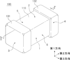
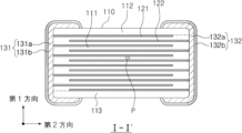
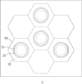
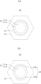
図1は、本発明の一実施形態による積層型電子部品を概略的に示した斜視図であり、図2は、図1の内部電極の積層構造を概略的に示した分離斜視図であり、図3は、図1のI-I'線に沿った断面図であり、図4は、図3の誘電体層の一部であるP領域に含まれた複数の誘電体結晶粒を概略的に示した図面であり、図5は、誘電体結晶粒を概略的に示した図面である。
[Laminated electronic components]
FIG. 1 is a perspective view schematically showing a multilayer electronic component according to an embodiment of the present invention, and FIG. 2 is an exploded perspective view schematically showing a multilayer structure of internal electrodes in FIG. 3 is a cross-sectional view taken along line II' in FIG. 1, and FIG. 4 schematically shows a plurality of dielectric crystal grains included in a P region that is a part of the dielectric layer in FIG. FIG. 5 is a drawing schematically showing dielectric crystal grains.
以下、図1~図5を参照して、本発明の一実施形態による積層型電子部品について詳細に説明する。 DESCRIPTION OF THE PREFERRED EMBODIMENTS A laminated electronic component according to an embodiment of the present invention will be described in detail below with reference to FIGS. 1 to 5.
本発明の一実施形態による積層型電子部品100は、複数の誘電体層111及び内部電極121、122を含む本体110、及び上記本体110の外側に配置されて上記内部電極121、122と連結される外部電極131、132を含み、上記誘電体層111は複数の誘電体結晶粒20を含み、上記複数の誘電体結晶粒20の少なくとも1つ以上は、内側のコア領域21、上記コア領域21の少なくとも一部を覆う第1及び第2インターフェースシェル領域22a、22bを含むインターフェースシェル領域22、及び上記インターフェースシェル領域22の少なくとも一部を覆うシェル領域23を含むコア21-インターフェースシェル22-シェル23構造を有し、上記コア21-インターフェースシェル22-シェル23構造を有する誘電体結晶粒は、ペロブスカイト(ABO3)系母材主成分、Siを含む第1副成分、並びにMn、V、Cr、Fe、Ni、Co、Cu、Zn及びSnからなる群から選択された一つ以上を含む第2副成分を含み、上記第1副成分の平均含有量は、第1インターフェースシェル領域22aで最も高く、上記第2副成分の平均含有量は、上記第2インターフェースシェル領域22bで最も高いことができる。
A multilayer
本体110は、誘電体層111及び内部電極121、122が交互に積層されている。
In the
本体110の具体的な形状に特に制限はないが、図示のように、本体110は六面体状またはこれと類似した形状からなることができる。焼成過程で本体110に含まれたセラミック粉末の収縮によって、本体110は完全な直線を有する六面体状ではないが、実質的に六面体状を有することができる。
Although there is no particular limitation on the specific shape of the
本体110は、第1方向に互いに向かい合う第1及び第2面1、2、第1及び第2面1、2と連結され、第2方向に互いに向かい合う第3及び第4面3、4、第1~第4面1、2、3、4と連結され、第3方向に互いに向かい合う第5及び第6面5、6を有することができる。
The
本体110を形成する複数の誘電体層111は焼成された状態であり、隣接する誘電体層111間の境界は走査電子顕微鏡(SEM:Scanning Electron Microscope)を利用せずには確認しにくいほど一体化することができる。
The plurality of
誘電体層111を形成する原料は、十分な静電容量を得ることができる限り制限されない。一般的に、ペロブスカイト(ABO3)系材料を用いることができ、例えば、チタン酸バリウム系材料、鉛複合ペロブスカイト系材料、またはチタン酸ストロンチウム系材料などを用いることができる。チタン酸バリウム系材料は、BaTiO3系セラミック粉末を含むことができ、セラミック粉末の例示として、BaTiO3、BaTiO3にCa(カルシウム)、Zr(ジルコニウム)などが一部固溶された(Ba1-xCax)TiO3(0<x<1)、Ba(Ti1-yCay)O3(0<y<1)、(Ba1-xCax)(Ti1-yZry)O3(0<x<1、0<y<1)またはBa(Ti1-yZry)O3(0<y<1)などが挙げられる。
The raw material for forming the
また、誘電体層111を形成する原料は、チタン酸バリウム(BaTiO3)などの粉末に本発明の目的に応じて様々なセラミック添加剤、有機溶剤、結合剤、分散剤などが添加されることができる。
In addition, the raw material for forming the
従来の60nm級サイズのチタン酸バリウム(BaTiO3)系誘電体粒子の形成過程は、まず、Ba(OH)2を設け、Ba(OH)2にTiO2を投入して、10nm級BaTiO3シード(seed)を形成する。この後、上記BaTiO3シード(seed)に金属酸化物などの添加剤を投入した後、高温/高圧環境で粒成長させて60nm級誘電体粒子を製造することができる。従来の製造方法で製造した誘電体粒子は、正方晶系構造(tetragonal structure)のコア直径は30nm級のサイズを有し、金属イオンがドープされた領域の立方晶系構造(cubic structure)の直径は、30nm級のサイズを有するようになる。 The conventional process of forming barium titanate (BaTiO 3 )-based dielectric particles with a size of 60 nm class is to first provide Ba(OH) 2 , add TiO 2 to Ba(OH) 2 , and form 10 nm class BaTiO 3 seeds. (seed). Thereafter, additives such as metal oxides are added to the BaTiO 3 seeds, and the particles are grown in a high temperature/high pressure environment to produce 60 nm class dielectric particles. The dielectric particles manufactured by the conventional manufacturing method have a core diameter of 30 nm in a tetragonal structure, and a cubic structure in a region doped with metal ions. has a size on the order of 30 nm.
すなわち、従来の製造方法では、コア内部への添加剤の拡散を抑制することが容易でなく、それに応じて誘電特性の制御が容易でないという問題点があった。例えば、60nm級のBaTiO3誘電体粒子の場合、正方晶系構造(tetragonal structure)を有するコアは30nm級のレベルに留まっている。 That is, in the conventional manufacturing method, there was a problem in that it was not easy to suppress the diffusion of the additive into the core, and it was not easy to control the dielectric properties accordingly. For example, in the case of BaTiO 3 dielectric particles of 60 nm class, the core having a tetragonal structure remains at a level of 30 nm class.
しかしながら、本発明の一実施形態のように、粒界抵抗を増大させることがあるSi及び酸素空孔(Oxygen vacancy)生成を抑制するアクセプタ(acceptor)元素を誘電体粒子の合成過程でそれぞれコート及びドープする場合、内部電極の劣化を防止すると同時に、誘電特性を向上させることができる効果がある。 However, in one embodiment of the present invention, Si, which can increase grain boundary resistance, and an acceptor element, which suppresses the generation of oxygen vacancies, are coated and coated, respectively, during the synthesis process of dielectric particles. Doping has the effect of preventing deterioration of the internal electrodes and improving dielectric properties at the same time.
追加的に、上記誘電体粒子に希土類元素などの添加剤をさらに添加して焼成熱処理する場合、信頼性が向上するとともに誘電特性が増大できる誘電体結晶粒を誘電体層の内部に含むことができる。 Additionally, when an additive such as a rare earth element is further added to the dielectric particles and subjected to firing heat treatment, the dielectric layer may contain dielectric crystal grains that can improve reliability and increase dielectric properties. can.
従来の誘電体粒子の製造方法のみでは、後述する第1インターフェースシェル22a及び第2インターフェースシェル22bを形成することが困難であり、それによる効果も実現し難い場合があり、以下でより詳細に説明する。
It is difficult to form the
図4を参照すると、誘電体層111は複数の誘電体結晶粒20を含むことができる。図4のP領域は、任意の誘電体層111を拡大して複数の誘電体結晶粒20を概略的に示したものである。
Referring to FIG. 4,
このとき、複数の誘電体結晶粒20、20'の少なくとも1つ以上は、内側のコア領域21、上記コア領域21の少なくとも一部を覆う第1及び第2インターフェースシェル領域22a、22bを含むインターフェースシェル領域22、及び上記インターフェースシェル領域22の少なくとも一部を覆うシェル領域23を含むコア21-インターフェースシェル22-シェル構造23を有することができる。
At this time, at least one of the plurality of
より具体的には、図5を参照すると、誘電体結晶粒20、20'のコア領域21は、内側の第1コア領域21a及び上記第1コア領域21aの少なくとも一部を覆う第2コア領域21bを含む第1コア21a-第2コア21b構造を有することができ、上記第1コア領域21aは正方晶系構造(tetragonal structure)を有し、上記第2コア領域21bは第2副成分を含み、立方晶系構造(cubic structure)を有することができる。このとき、第2コア領域21bに第2副成分が含まれることで、第2コア領域21bのペロブスカイト(ABO3)系構造が立方晶系構造(cubic structure)となり得る。
More specifically, referring to FIG. 5, the
誘電体の母材主成分として用いるBaTiO3、(Ba、Ca)(Ti、Ca)O3、(Ba、Ca)(Ti、Zr)O3、及びBa(Ti、Zr)O3は、ABO3で表されるペロブスカイト(perovskite)系構造に該当し、熱処理工程の進行中に酸素が存在すべき位置に欠陥が生じる酸素空孔(oxygen vacancy)が発生することがある。例えば、還元雰囲気で焼成を行う場合、酸素空孔(oxygen vacancy)が発生することがあり、または脱バインダーなどによってカーボンがABO3の酸素と結合してCO2形態で蒸発する場合にも酸素空孔(oxygen vacancy)が発生する可能性がある。酸素(O)原子は-2価の電荷(charge)を帯びるようになるが、酸素が存在すべき位置に欠陥が生じると、+2価の電荷(charge)を有する酸素空孔(oxygen vacancy)が発生し、印加した電界によって酸素空孔が移動すると信頼性が低下し、酸素空孔(oxygen vacancy)が多いほど、そして温度及び電圧が高くかかるほど酸素空孔(oxygen vacancy)の移動速度及び移動量が増加して、信頼性をさらに悪化させるようになり、このような工程環境は、高温焼成で主に発生することがある。このような酸素空孔(oxygen vacancy)の問題点を解決するために、一般的に他の金属酸化物などの添加剤や副成分などをドープすることができるが、このとき、チタン(Ti)及び酸化水は同一であるが、イオン半径が異なる元素を一部置換することができる。添加される添加剤として、Mn、V、Cr、Fe、Ni、Co、Cu、Zn及びSnからなる群から選択された一つ以上を含むことができるが、特にこれに制限されるものではなく、焼成工程後の誘電体層111に含まれた複数の誘電体結晶粒20の少なくとも1つ以上は、上記添加剤を副成分として含むようになることで、立方晶系構造(cubic structure)を有することができる。
BaTiO 3 , (Ba, Ca) (Ti, Ca) O 3 , (Ba, Ca) (Ti, Zr) O 3 and Ba (Ti, Zr) O 3 used as the main components of the dielectric base material are ABO It corresponds to a perovskite structure represented by 3 , and oxygen vacancies, which are defects in positions where oxygen should exist, may occur during the heat treatment process. For example, when firing is performed in a reducing atmosphere, oxygen vacancies may be generated, or when carbon combines with oxygen in ABO 3 and evaporates in the form of CO 2 due to binder removal, oxygen vacancies may occur. Oxygen vacancies may occur. Oxygen (O) atoms come to carry a charge of -2 valence, but when a defect occurs at a position where oxygen should exist, an oxygen vacancy with a charge of +2 valence occurs. Reliability decreases when oxygen vacancies move due to the generated and applied electric field, and the more oxygen vacancies there are, and the higher the temperature and voltage applied, the faster the oxygen vacancies move and move. The amount increases, further deteriorating the reliability, and such a process environment may mainly occur in high temperature firing. In order to solve the problem of oxygen vacancies, additives and subcomponents such as other metal oxides can generally be doped. and oxidized water are the same, but elements with different ionic radii can be partially substituted. The additive to be added may include one or more selected from the group consisting of Mn, V, Cr, Fe, Ni, Co, Cu, Zn, and Sn, but is not particularly limited thereto. At least one of the plurality of
一般的に、BaTiO3系誘電体は、常温で正方晶系構造(tetragonal structure)を有するが、一部元素が置換された領域は、立方晶系構造(cubic structure)の格子構造に変形することができ、このように格子構造を変形して双極子(dipole)モーメントのある相に切り替えることで、自体誘電率を高めて、粒成長なしに小さなサイズを有すると同時に、高誘電率を確保することができる。これによって、超薄層の誘電体層を形成することができ、積層型電子部品の超小型化を達成することができる。 In general, BaTiO3 -based dielectrics have a tetragonal structure at room temperature, but regions where some elements are substituted can transform into a cubic structure. By changing the lattice structure and switching to a phase with a dipole moment, it is possible to increase the dielectric constant of itself and have a small size without grain growth while ensuring a high dielectric constant. be able to. This makes it possible to form an ultra-thin dielectric layer and achieve ultra-miniaturization of the laminated electronic component.
一般的に、誘電率は立方晶系構造(cubic structure)を有する領域のサイズに対して、正方晶系構造(tetragonal structure)を有する領域のサイズが大きい場合に向上することが知られており、換言すると、同じサイズを有する誘電体粒子のうち、tetragonal structure size/cubic structure sizeの割合が大きい誘電体粒子であるほど誘電率が向上する。 Generally, it is known that the dielectric constant improves when the size of the region having a tetragonal structure is larger than the size of the region having a cubic structure. In other words, among dielectric particles having the same size, a dielectric particle with a larger ratio of tetragonal structure size/cubic structure size has a higher dielectric constant.
本明細書で誘電体結晶粒20、20'の一構成に関して説明する平均直径サイズは、SEM(Scanning Electron Microscope)またはTEM(Transmission Electron Microscope)イメージから確認できる誘電体結晶粒のコア21の中心から一直線を引いた後、一直線上に位置した各構成の最小距離と最大距離との差を測定し、このような最小距離と最大距離との差を様々な角度で測定して平均した値であることができる。但し、これに限定するものではなく、誘電体結晶粒20の各構成の特徴によって相違に測定することができる。
The average diameter size described herein with respect to one configuration of
本発明の一実施形態による積層型電子部品のうち、誘電体結晶粒20、20'のコア領域21の平均直径サイズは、55nm以上65nm以下であることができる。このとき、上記コア領域21のうち、第1コア領域21aの平均直径サイズは45nm以上55nm以下であることができ、上記コア21のうち、第2コア領域21bの平均直径サイズは5nm以上15nm以下であることができる。
In the multilayer electronic component according to an embodiment of the present invention, the average diameter size of the
焼成後の誘電体結晶粒20、20'のコア領域21の平均直径サイズは、焼成前の誘電体粒子のサイズであることができるが、特にこれに制限されるものではない。但し、後述するSiを含む第1副成分によって第2コア領域21bの平均直径サイズが従来の誘電体粒子を焼成した場合より小さいことがある。
The average diameter size of the
上記第2コア領域21bの平均直径サイズが5nm以下である場合、酸素空孔(oxygen vacancy)を効果的に抑制することが困難であり、第2コア領域21bの平均直径サイズが15nm超過である場合、過度の第2副成分のドープによって、正方晶系構造(tetragonal structure)の領域が小さくなって、誘電率が低下する可能性がある。 When the average diameter size of the second core region 21b is less than 5 nm, it is difficult to effectively suppress oxygen vacancies, and when the average diameter size of the second core region 21b exceeds 15 nm. In this case, excessive doping of the second subcomponent may reduce the area of the tetragonal structure and lower the dielectric constant.
上記コア領域21の少なくとも一部を覆うインターフェースシェル領域22は、第1インターフェースシェル22a及び第2インターフェースシェル領域22bを含むことができる。
The
より具体的には、図5の(b)を参照すると、コア21-インターフェースシェル22-シェル23構造を有する誘電体結晶粒20'のうち、コア21領域の表面を少なくとも一部覆う第1インターフェースシェル22a及び第2コアインターフェースシェル22bは、コア21を同時に覆うことができ、本図面では、第1及び第2インターフェースシェル22a、22bが重ならない形状で示したが、これに限定されるものではなく、一部領域で重なっている形状になることができ、形成された第1及び第2インターフェースシェル22a、22bのうち、大きな領域を有するインターフェースシェルが小さい領域を有するインターフェースシェルを含む形状になることもできる。
More specifically, referring to FIG. 5B, among the dielectric crystal grains 20' having a core 21-interface shell 22-
第1インターフェースシェル22a及び第2インターフェースシェル領域22bに最も多く含まれた副成分の含有量は互いに相違することができ、例えば、第1インターフェースシェル領域22aに含まれた副成分はSiを含む第1副成分を意味することができ、第2インターフェースシェル領域22bに含まれた副成分は、Mn、V、Cr、Fe、Ni、Co、Cu、Zn及びSnからなる群から選択された1つ以上を含む第2副成分を意味することができる。
The contents of the subcomponent contained most in the
より具体的には、コア21-インターフェースシェル22-シェル23構造を有する誘電体結晶粒20、20'は、チタン酸バリウム(BaTiO3)系母材を主成分とし、Siを含む第1副成分及び上記第2副成分を含むことができる。ここで、第1副成分の平均含有量は、第1インターフェースシェル領域22aで最も高いことができ、第2副成分の平均含有量は、第2インターフェースシェル領域22bで最も高いことができる。
More specifically, the
焼成工程前、誘電体粒子状態の第1インターフェース領域22aにSiが含まれることで、第2インターフェース領域22bの第2副成分がコア内部に拡散することを抑制することができ、これによって比較的小さい平均直径サイズを有する第2コア領域21bが形成されることができる。これにより、第2副成分による酸素空孔の抑制効果によって信頼性を向上させるとともに、コア21の正方晶系構造(tetragonal structure)を有する第1コア領域21aのサイズを立方晶系構造(cubic structure)を有する第2コア領域22bのサイズに対して大きく維持することができ、高い誘電率を有する積層型電子部品を実現することができる。
By including Si in the
また、第1インターフェース領域22aに含まれたSiの含有量が高い場合、すなわち、Siを含む第1インターフェース領域21aが形成されることで、Siによる液相形成により、第1インターフェースシェル領域22bがない従来の場合よりも、同一誘電容量及びDFを実現するために、焼成温度を約5℃~約10℃程度下げることができ、焼成温度が低くなるにつれて超薄層の内部電極121、122で劣化を防止することができる効果がある。
Further, when the content of Si contained in the
図5の(a)及び(b)を参照して説明すると、以下のとおりである。上記コア領域21の少なくとも一部を覆うインターフェースシェル領域22は、第1インターフェースシェル領域22a及び第2インターフェースシェル領域22bを含むことができ、第1インターフェースシェル22a及び第2インターフェースシェル22bは、それぞれコア領域21の表面を覆うことができるが、コア領域21の表面を同時に覆うことが好ましい。
The explanation will be as follows with reference to FIGS. 5(a) and 5(b). The
このとき、第1インターフェースシェル領域22aの平均直径サイズは、2nm以上5nm以下であることができる。ここで、第1インターフェースシェル領域22aの平均直径サイズは、第1インターフェースシェル領域22aの平均厚さを意味することができる。
At this time, the average diameter size of the first
ここで、第1インターフェースシェル領域22aの直径サイズは、誘電体結晶粒20'のコアの中心から一直線上に位置したコア21の外側から近い第1インターフェースシェル領域22aの地点と、コア21から離れた第1インターフェースシェル領域22aの地点の直径を意味することができる。第1インターフェースシェル22aは、コア21の表面を覆うことができ、一定の面積を有する場合、様々な角度で測定した第1インターフェースシェル領域21aの直径を測定して平均した値であり、上記平均値は、第1インターフェースシェル領域22aの平均直径サイズを意味することができる。このような測定方法は、後述する第2インターフェースシェル領域22bの直径サイズ及び平均直径サイズにも適用することができる。
Here, the diameter size of the first
また他の方法では、第1インターフェース領域22a及び第2インターフェース領域22bの平均直径サイズは、Gaussian fitting方法を用いて求めることができる。ここで、Gaussian fitting方法は、ガウス関数を用いてFWHM(Full Width at Half Maximum)を求めることができる公式に該当する。TEMにおいて、第1及び第2インターフェースシェル領域22a、22bをそれぞれline profile raw dataを用いてデータを得た後、下記(数1)式に該当するGaussian fitting数式を適用してノイズを除去し、導出されるグラフのピーク(peak)値の範囲を測定して求めたサイズを10個のline profile raw dataに拡張して求めた平均値であることができ、dataのサンプルが多いほど求めようとする平均値を導出する上で好ましい。
In yet another method, the average diameter size of the
インターフェースシェル22は、TEM-EDSイメージから確認できるように、一定の直径サイズを有することができ、より具体的な平均直径サイズ(厚さ)は、Gaussian fittingを介して具体的に測定することができる。
The
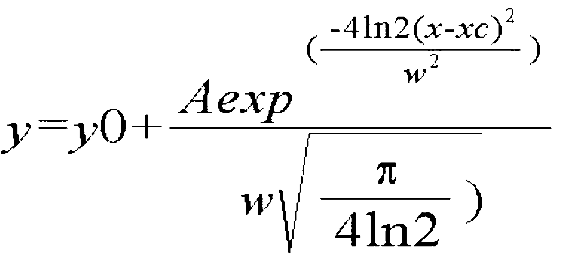
(y0=base、xc=x value at center、A=area、w=FWHM)
(y0=base, xc=x value at center, A=area, w=FWHM)
一方、第1インターフェースシェル領域22aの平均直径サイズが2nm未満である場合、十分な粒界抵抗効果を実現することが困難であり、第1インターフェースシェル領域22aの平均直径サイズが5nm超過である場合、粒界抵抗効果は増大することができるが、誘電率が低下するという問題点が発生する可能性がある。
On the other hand, when the average diameter size of the first
一方、第1インターフェースシェル領域22aは、上記コア領域の表面を20%以上50%以下覆うことができる。第1インターフェースシェル領域22aが覆うコア領域21の表面が20%未満である場合、十分な粒界抵抗効果を実現し難く、第1インターフェースシェル領域22aが覆うコア領域の表面が50%超過である場合、粒界抵抗効果は増大することができるが、誘電率が低下するという問題点が発生する可能性がある。
Meanwhile, the first
また、第2インターフェースシェル領域22bの平均直径サイズは、3nm以上10nm以下であることができる。ここで、第2インターフェースシェル領域22bの平均直径サイズは、第2インターフェースシェル領域22bの平均厚さを意味することができる。
Further, the average diameter size of the second
第2インターフェースシェル領域22bの平均直径サイズが3nm未満である場合、十分な酸素空孔の抑制効果を実現することが困難であり、第2インターフェースシェル領域22bの平均直径サイズが10nm超過である場合、酸素空孔の抑制効果は増大することができるが、誘電率が低下するという問題点が発生する可能性がある。
If the average diameter size of the second
一方、第2インターフェースシェル領域22bは、上記コア領域21の表面を35%以上80%以下覆うことができる。第2インターフェースシェル領域22bが覆うコア領域21の表面が35%未満である場合、十分な酸素空孔の抑制効果を実現し難く、第2インターフェースシェル領域22bが覆うコア領域21の表面が80%超過である場合、酸素空孔の抑制効果は増大することができるが、誘電率が低下するという問題点が発生する可能性がある。
Meanwhile, the second
本発明の一実施形態によると、第1及び第2インターフェースシェル領域22a、22bの平均直径サイズが大きくなるほど、コア領域21の表面を覆う割合は増加する傾向を示したが、特にこれに制限されるものではなく、平均直径サイズが小さい場合でもコア21を覆う領域が大きいことができ、逆に平均直径サイズが大きい場合でもコア21を覆う領域が小さいことができる。
According to an embodiment of the present invention, as the average diameter size of the first and second
また、誘電体結晶粒のシェル領域23は、インターフェースシェル領域22の少なくとも一部を覆うことができ、インターフェースシェル22の外側から結晶粒界(grain boundary)までの領域を意味することができる。
Further, the dielectric
誘電体結晶粒20には、La、Y、Ac、Ce、Pr、Nd、Pm、Sm、Eu、Gd、Tb、Dy、Ho、Er、Tm、Yb及びLuからなる群から選択された1つ以上を含む希土類元素が含まれることができ、より具体的には、上記希土類元素の平均含有量は、コア21-インターフェースシェル22-シェル23構造を有する誘電体結晶粒20、20'のうち、シェル領域23で最も高いことができる。これは、第1インターフェースシェル22aによってコア21内部への拡散が抑制されたものと見なすことができ、これにより、希土類元素による信頼性が向上すると同時に、誘電特性がさらに向上することができる。
The
希土類元素はチタン酸バリウム(BaTiO3)系の元素位置を効果的に置換することができ、酸素空孔の欠陥濃度の減少に効果的であり、過度の結晶粒成長を抑制して信頼性低下を防止することができる。 Rare earth elements can effectively substitute element positions in barium titanate (BaTiO 3 ) system, and are effective in reducing the defect concentration of oxygen vacancies, suppressing excessive grain growth and reducing reliability. can be prevented.
図6は、本発明の一実施形態による積層型電子部品の誘電体層111に含まれた誘電体結晶粒の一結晶粒界(grain boundary)から他の結晶粒界(grain boundary)までの第1副成分であるSi、第2副成分であるSn、希土類元素であるDy元素含有量を測定したline-profileグラフである。
FIG. 6 shows the distance from one grain boundary of a dielectric crystal grain to another grain boundary included in a
まず、Sn元素含有量を確認すると、約17.11nmから約19.97nm領域にピーク(peak)が形成されたことが確認でき、これによってコア21領域の一外側に第2インターフェースシェル領域22bが形成されたことが分かる。Si元素含有量を確認すると、約84.00nmから約88.42nmの領域にピーク(peak)が形成されたことが確認でき、これによってコア領域21の他の外側に第1インターフェースシェル領域22aが形成されたことが分かる。
First, when checking the Sn element content, it was confirmed that a peak was formed in the region from about 17.11 nm to about 19.97 nm, and this caused the second
図7及び図8は、本発明の一実施例及び比較例の誘電体結晶粒を撮影したTEM-EDSイメージである。 7 and 8 are TEM-EDS images of dielectric crystal grains of an example of the present invention and a comparative example.
より具体的には、図7の(a)は、本発明の一実施形態の誘電体結晶粒であり、Siを含む第1インターフェースシェル領域22aがコア領域21の表面を20%以上50%以下覆う場合のTEM-EDSイメージである。矢印で示したように、一定の厚さの第1インターフェース領域22aがあることが確認できる。図7の(b)は、比較例の誘電体結晶粒として、従来の製造方法で製造した誘電体粒子を焼成した場合のTEM-EDSイメージである。従来の製造方法で製造した誘電体粒子を生成した後に、Siを添加剤として添加したが、第1インターフェース領域22aが形成されなかったことが確認できる。図7の(c)は、比較例の誘電体結晶粒として、第1インターフェースシェル領域22aがコア領域21の表面を20%未満覆う場合のTEM-EDSイメージである。矢印で示した領域に第1インターフェースシェル領域22aが薄くあることが確認できるが、図7の(a)のように明確に形成されておらず、これから粒界抵抗効果が十分に発揮されないことが予想される。
More specifically, (a) of FIG. 7 shows a dielectric crystal grain according to an embodiment of the present invention, in which the first
図8の(a)は、本発明の一実施形態による誘電体結晶粒のSi、Sn、Dy元素を撮影したTEM-EDSイメージであり、Siイメージは図7の(a)と同一である。Snを含む第2インターフェースシェル領域22bがコア領域21の表面を覆っており、第1インターフェースシェル領域22aと類似した領域に形成され、一定の厚さを有して形成されたことが確認でき、希土類元素であるDyがコア21の内部に拡散されないままシェル領域23に主に含まれていることが確認できる。図8の(b)は、比較例の誘電体結晶粒であり、Siイメージは図7の(b)と同一である。Snがコア領域21を囲んだ形態で形成されているが、一定の厚さに形成されていないため、第2インターフェースシェル領域22bを明確に区別し難く、これからコア21内部への拡散が発生して正方晶系構造(cubic structure)を有する領域が比較的大きいことが予想でき、希土類元素であるDyが含まれていることが確認できる。
FIG. 8(a) is a TEM-EDS image of Si, Sn, and Dy elements of a dielectric crystal grain according to an embodiment of the present invention, and the Si image is the same as FIG. 7(a). It can be confirmed that the second
一方、誘電体層111の厚さtdは特に限定する必要はない。但し、積層型電子部品の小型化及び高容量化をより容易に達成するために、内部電極121、122の厚さは0.6μm以下であることができ、より好ましくは0.4μm以下であることができる。ここで、誘電体層111の厚さtdは、誘電体層111の平均厚さtdを意味することができる。
On the other hand, the thickness td of the
誘電体層111の平均厚さtdは、第1及び第2内部電極121、122の間に配置される誘電体層111の平均厚さを意味することができる。
The average thickness td of the
誘電体層111の平均厚さtdは、本体110の長さ及び厚さ方向(L-T)の断面を1万倍率の走査電子顕微鏡(SEM)を用いてイメージをスキャンして測定することができる。より具体的には、スキャンされたイメージから1つの誘電体層を長さ方向に等間隔である30つの地点でその厚さを測定した平均値を測定することができる。上記等間隔である30つの地点は、活性部Acで指定されることができる。また、このような平均値測定を10つの誘電体層に拡張して平均値を測定すると、誘電体層111の平均厚さtdをさらに一般化することができる。ここで、誘電体層111の平均厚さtdは、誘電体層111の第1方向の平均サイズを意味することができる。
The average thickness td of the
本体110は、本体110の内部に配置され、誘電体層111を間に挟んで互いに向かい合うように配置される第1内部電極121及び第2内部電極122を含んで容量が形成される活性部Acと、活性部の第1方向の両端面に形成された上部及び下部カバー部112、113を含むことができ、活性部Acの第3方向の両側面上には、マージン部114、115が配置されることができる。
The
活性部Acは、積層型電子部品の容量形成に寄与する部分であって、誘電体層111を間に挟んで複数の第1及び第2内部電極121、122を繰り返し積層して形成されることができる。
The active part Ac is a part that contributes to capacitance formation of the multilayer electronic component, and is formed by repeatedly stacking a plurality of first and second
カバー部112、113は、活性部Acの第1方向の上部に配置される上部カバー部112及び活性部Acの第1方向の下部に配置される下部カバー部113を含むことができる。
The
上部カバー部112及び下部カバー部113は、単一誘電体層111または2つ以上の誘電体層111を活性部Acの上下面にそれぞれ第1方向(厚さ方向)に積層して形成することができ、基本的には、物理的または化学的ストレスによる内部電極121、122の損傷を防止する役割を果たすことができる。
The
上部カバー部112及び下部カバー部113は、内部電極121、122を含まず、誘電体層111と同一材料を含むことができる。すなわち、上部カバー部112及び下部カバー部113は、セラミック材料を含むことができ、例えば、チタン酸バリウム(BaTiO3)系セラミック材料を含むことができる。
The
カバー部112、113の平均厚さtcは特に限定する必要はない。但し、積層型電子部品の小型化及び高容量化をより容易に達成するために、カバー部112、113の平均厚さtcは30μm以下であることができ、超小型製品ではより好ましくは20μm以下であることができる。
The average thickness tc of the
カバー部112、113の平均厚さtcは、本体110の長さ及び厚さ方向(L-T)の断面を1万倍率の走査電子顕微鏡(SEM)を用いてイメージをスキャンして測定することができる。より具体的には、スキャンされたイメージにおいて、1つのカバー部112、113を長さ方向に等間隔である30つの地点でその厚さを測定した平均値を測定することができる。上記等間隔である30つの地点は、上部カバー部112、113で指定されることができる。また、このような平均値の測定を上部及び下部カバー部112、113に拡張して平均値を測定すると、カバー部112、113の平均厚さtdをさらに一般化することができる。ここで、カバー部112、113の平均厚さtcは、カバー部112、113の第1方向の平均サイズを意味することができる。
The average thickness tc of the
一方、マージン部114、115は、本体110の第5面5に配置された第1マージン部114及び第6面6に配置された第2マージン部115を含むことができる。すなわち、マージン部114、115は、本体110の第3方向(幅方向)の両側面に配置されることができる。
Meanwhile, the margin parts 114 and 115 may include a first margin part 114 disposed on the
マージン部114、115は、図2に示したように、本体110の厚さ及び幅方向(W-T方向)の断面(cross-section)に基づいて、第1及び第2内部電極121、122の第3方向の両側面と本体110の境界面との間の領域を意味することができる。
As shown in FIG. 2, the margin parts 114 and 115 are formed by forming the first and second
マージン部114、115は、基本的に物理的または化学的ストレスによる内部電極121、122の損傷を防止する役割を果たすことができる。
The margin parts 114 and 115 can basically serve to prevent damage to the
マージン部114、115は、セラミックグリーンシート上にマージン部114、115が形成されるところを除いて、導電性ペーストを塗布して内部電極121、122を形成することで形成されたものであることができる。上述したように、内部電極121、122による段差を抑制するために、積層後に内部電極121、122が本体110の第5及び第6面5、6に露出するように切断した後、単一誘電体層111または2つ以上の誘電体層111を活性部Acの両側面に第3方向(幅方向)に積層してマージン部114、115を形成することもできる。
The margin parts 114 and 115 are formed by applying conductive paste to form the
第1及び第2マージン部114、115の平均幅は、特に限定する必要はない。但し、積層型電子部品100の小型化及び高容量化をより容易に達成するために、第1及び第2マージン部114、115の平均幅は30μm以下であり、超小型製品においてより好ましくは20μm以下であることができる。
The average width of the first and second margin portions 114 and 115 does not need to be particularly limited. However, in order to more easily achieve miniaturization and high capacity of the multilayer
マージン部114、115の平均幅は、本体110の幅及び厚さ方向(W-T)の断面を1万倍率の走査電子顕微鏡(SEM)を用いてイメージをスキャンして測定することができる。より具体的に、スキャンされたイメージにおいて1つのマージン部114、115を厚さ方向に等間隔である10つの地点でその幅を測定した平均値を測定することができる。上記等間隔である10つの地点は、第1マージン部114で指定することができる。また、このような平均値の測定を第1及び第2マージン部114、115に拡張して平均値を測定すると、マージン部114、115の平均幅をさらに一般化することができる。ここで、マージン部114、115の平均幅は、マージン部114、115の第3方向の平均サイズを意味することができる。
The average width of the margin parts 114 and 115 can be measured by scanning an image of a cross section of the
内部電極121、122は誘電体層111と交互に積層されることができる。内部電極121、122は第1内部電極121及び第2内部電極122を含むことができ、第1及び第2内部電極121、122は本体110を構成する誘電体層111を間に挟んで互いに向かい合うように交互に配置され、本体110の第3及び第4面3、4にそれぞれ露出することができる。
The
第1内部電極121は第4面4から離隔して、第3面3を介して露出し、第2内部電極122は第3面3から離隔して、第4面4を介して露出することができる。本体110の第3面3には第1外部電極131が配置されて第1内部電極121と連結され、本体110の第4面4には第2外部電極131が配置されて第2内部電極122と連結されることができる。
The first
すなわち、第1内部電極121は第2外部電極132とは連結されず、第1外部電極131と連結され、第2内部電極122は第1外部電極131とは連結されず、第2外部電極132と連結されることができる。このとき、第1及び第2内部電極121、122は、中間に配置された誘電体層111によって互いに電気的に分離されることができる。
That is, the first
一方、本体110は、第1内部電極121が印刷されたセラミックグリーンシートと第2内部電極122が印刷されたセラミックグリーンシートを交互に積層した後、焼成して形成されることができる。
Meanwhile, the
内部電極121、122を形成する材料は特に制限されず、電気導電性に優れた材料を用いることができる。例えば、内部電極121、122は、ニッケル(Ni)、銅(Cu)、パラジウム(Pd)、銀(Ag)、金(Au)、白金(Pt)、スズ(Sn)、タングステン(W)、チタン(Ti)及びこれらの合金のうち1つ以上を含む内部電極用導電性ペーストをセラミックグリーンシートに印刷して形成することができる。内部電極用導電性ペーストの印刷方法は、スクリーン印刷法やグラビア印刷法などを用いることができるが、本発明がこれに限定されるものではない。
The material forming the
一方、内部電極121、122の平均厚さteは、特に限定する必要はない。
On the other hand, the average thickness te of the
但し、一般的に内部電極121、122の厚さを0.6μm未満の薄層に形成する場合、特に内部電極121、122の厚さが0.4μm以下である場合には、信頼性が低下するおそれがある。しかしながら、本発明の一実施形態によって誘電体結晶粒20に第1インターフェースシェル22aが含まれることで、比較的低い温度で焼成工程を行うことができ、内部電極121、122の劣化を防止して、内部電極121、122の平均厚さteが0.4μm以下である場合にも優れた信頼性を確保することができる。
However, in general, when forming the
内部電極121、122の平均厚さteは、本体110の長さ及び厚さ方向(L-T)の断面を1万倍率の走査電子顕微鏡(SEM、Scanning Electron Microscope)を用いてイメージをスキャンして測定することができる。より具体的には、スキャンされたイメージにおいて1つの内部電極121、122を長さ方向に等間隔である30つの地点でその厚さを測定して平均値を測定することができる。上記等間隔である30つの地点は、活性部Acで指定されることができる。また、このような平均値の測定を10個の内部電極121、122に拡張して平均値を測定すると、内部電極121、122の平均厚さをさらに一般化することができる。ここで、内部電極121、122の平均厚さteは、内部電極121、122の第1方向の平均サイズを意味することができる。
The average thickness te of the
本発明の一実施形態では、セラミック電子部品100が2つの外部電極131、132を有する構造を説明しているが、外部電極131、132の個数や形状などは、内部電極121、122の形態やその他の目的に応じて変更することができる。
In one embodiment of the present invention, a structure in which the ceramic
外部電極131、132は、本体110の第3及び第4面3、4に配置されることができる。より具体的には、外部電極131、132は、本体110の第3及び第4面3、4にそれぞれ配置され、第1及び第2内部電極121、122とそれぞれ連結される第1及び第2電極層131a、132aを含むことができる。
The
一方、外部電極131、132は、金属などのように電気導電性を有するものであれば、どのような物質を用いても形成されることができ、電気的特性、構造的安定性などを考慮して、具体的な物質が決定されることができ、さらに多層構造を有することができる。
On the other hand, the
外部電極131、232は、導電性金属及びガラス(glass)を含む焼成電極であるか、導電性金属及び樹脂を含む樹脂系電極を含むことができる。
The
例えば、外部電極131、132は、本体110に配置される電極層131a、132a及び電極層131a、132a上に形成されためっき層131b、132bを含むことができる。電極層131a、132aに対するより具体的な例を挙げると、電極層131a、132aは、導電性金属及びガラスを含む焼成電極であるか、導電性金属及び樹脂を含む樹脂系電極であることができる。また、電極層131a、132aは、本体110上に焼成電極及び樹脂系電極が順次形成された形態であることができる。また、電極層131a、132aは、本体110上に導電性金属を含むシートを転写する方式で形成するか、焼成電極上に導電性金属を含むシートを転写する方式で形成されたものであることができる。電極層131a、132aに含まれる導電性金属として電気導電性に優れた材料を用いることができ、特に限定されない。例えば、導電性金属は、ニッケル(Ni)、銅(Cu)及びそれらの合金のうち1つ以上であることができる。
For example, the
めっき層131b、132bは実装特性を向上させる役割を果たし、導電性金属または焼成電極を含む電極層131a、132a上に配置されることができる。
The plating layers 131b and 132b serve to improve mounting characteristics and can be disposed on the
めっき層131b、132bの種類は特に限定されず、ニッケル(Ni)、スズ(Sn)、パラジウム(Pd)及びこれらの合金のうち1つ以上を含む単一層のめっき層131b、132bであることができ、複数層で形成されることができる。
The types of plating
めっき層131b、132bに対するより具体的な例を挙げると、めっき層131b、132bは、Niめっき層またはSnめっき層であることができ、めっき層131a、132a上にNiめっき層及びSnめっき層が順次形成された形態であることができ、Snめっき層、Niめっき層及びSnめっき層が順次形成された形態であることができる。また、めっき層131b、132bは、複数のNiめっき層及び/または複数のSnめっき層を含むこともできる。
To give a more specific example of the plating layers 131b and 132b, the plating layers 131b and 132b can be a Ni plating layer or a Sn plating layer, and a Ni plating layer and a Sn plating layer are formed on the
積層型電子部品100のサイズは特に限定する必要はない。
The size of the laminated
但し、小型化及び高容量化を同時に達成するためには、誘電体層111及び内部電極121、122の厚さを薄くして積層数を増加させることが好ましい。また、誘電体層111及び内部電極121、122の薄層化に伴う電界下で内部電極の劣化防止の効果を実現することができる本発明の効果は、0402(長さ×幅、0.4mm×0.2mm)以下のサイズを有する積層型電子部品100において、本発明による信頼性及び単位体積当たりの容量向上の効果がより顕著になる。
However, in order to simultaneously achieve miniaturization and high capacity, it is preferable to reduce the thickness of the
以下では、本発明の一実施例と比較例について特性評価を行ったことを詳細に説明する。 Below, characteristic evaluations of an example of the present invention and a comparative example will be explained in detail.
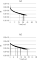
図9及び図10は、比較例及び本発明の一実施形態の超加速寿命試験(HALT、Highly Accelerated Life Test)のグラフである。 9 and 10 are graphs of a highly accelerated life test (HALT) of a comparative example and an embodiment of the present invention.
より具体的には、図9は、比較例のHALTグラフであり、(a)は温度条件115℃、電圧条件1.2Vrで72時間進行したものであり、MTTF(Mean Time To Failure)は39.6時間である。(b)は温度条件115℃、電圧条件1.5Vrで72時間進行したものであり、MTTFは16.2時間である。同一比較例の初期IR値は5.66×10^6であり、IR劣化程度を意味する傾き値である(log(初期IR/後期IR))は3.16と測定された。 More specifically, FIG. 9 is a HALT graph of a comparative example, and (a) shows the HALT graph that progressed for 72 hours under a temperature condition of 115° C. and a voltage condition of 1.2 Vr, and the MTTF (Mean Time To Failure) was 39. .6 hours. In (b), the test progressed for 72 hours under a temperature condition of 115° C. and a voltage condition of 1.5 Vr, and the MTTF was 16.2 hours. The initial IR value of the same comparative example was 5.66×10^6, and the slope value (log (initial IR/late IR)) indicating the degree of IR deterioration was measured to be 3.16.
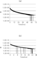
図10は、本発明の一実施形態のHALTグラフであり、実験条件は図9と同一である。すなわち、(a)は温度条件115℃、電圧条件1.2Vrで72時間進行したものであり、MTTFは22.5時間である。(b)は温度条件115℃、電圧条件1.5Vrで72時間進行したものであり、MTTFは22.5時間である。同一実施例の初期IR値は8.28×10^6であり、IR劣化程度を意味する傾き値である(log(初期IR/後期IR))は2.53と測定された。 FIG. 10 is a HALT graph of an embodiment of the present invention, and the experimental conditions are the same as in FIG. 9. That is, in (a), the test progressed for 72 hours under a temperature condition of 115° C. and a voltage condition of 1.2 Vr, and the MTTF was 22.5 hours. In (b), the test progressed for 72 hours under a temperature condition of 115° C. and a voltage condition of 1.5 Vr, and the MTTF was 22.5 hours. The initial IR value of the same example was 8.28×10^6, and the slope value (log (initial IR/late IR)) indicating the degree of IR deterioration was measured to be 2.53.
まとめると、比較例及び実施例を同一条件で実験した場合、(a)条件でのMTTFは39.6時間から57.9時間に約46%改善されたことが確認でき、(b)条件でのMTTFは16.2時間から22.5時間に約39%改善されたことが確認できる。初期IR値も5.66×10^6から8.28×10^6に改善され、IR劣化程度の把握のための傾き値(log(初期IR/後期IR))も3.16から2.53に改善されて、同一温度及び電圧条件を同一時間に進行したとき、IR劣化が減少することが確認できる。 In summary, when the comparative example and the example were tested under the same conditions, it was confirmed that the MTTF under the condition (a) was improved by about 46% from 39.6 hours to 57.9 hours, and under the condition (b). It can be confirmed that the MTTF of was improved by about 39% from 16.2 hours to 22.5 hours. The initial IR value was also improved from 5.66 x 10^6 to 8.28 x 10^6, and the slope value (log (initial IR/late IR)) used to understand the degree of IR deterioration also improved from 3.16 to 2. 53, and it can be confirmed that IR deterioration is reduced when the same temperature and voltage conditions are applied for the same time.
一方、下記の表1は、誘電体粒子の製造過程で投入したSi含有量に応じた積層型電子部品で検出されたSi含有量、MTTF、誘電率を測定したデータである。添加剤に含まれたSiの影響で初期投入したSiよりもさらに多いSiが検出された。Siが増加するほど粒界抵抗が増加して、MTTFが増加する傾向を示したが、誘電率が低くなることが確認できる。 On the other hand, Table 1 below shows data obtained by measuring the Si content, MTTF, and dielectric constant detected in multilayer electronic components according to the Si content added during the manufacturing process of dielectric particles. Due to the influence of Si contained in the additive, even more Si than initially added was detected. It can be confirmed that as Si increases, the grain boundary resistance increases and the MTTF tends to increase, but the dielectric constant decreases.
検出されたSi含有量は、誘電体結晶粒の第1インターフェース領域でTEMを用いてdetectingされたSi含有量に対するデータを意味する。 The detected Si content refers to data on the Si content detected using a TEM in the first interface region of the dielectric crystal grains.
MTTFは、温度条件125℃、電圧条件1.2Vrで超加速寿命試験(HALT)を行った場合の絶縁破壊平均時間を意味する。 MTTF means the average dielectric breakdown time when a hyper accelerated life test (HALT) is performed under a temperature condition of 125° C. and a voltage condition of 1.2 Vr.

誘電体粒子の形成時に、第1インターフェースシェルとなり得るSiの含有量が増加するほど、焼成後に誘電体結晶粒の第1インターフェースシェルで検出されたSiの含有量が増加することが確認でき、MTTFが増加したことが確認できる。但し、Siが過度に添加された場合、誘電率が減少したことが確認できる。これにより、優れたMTTF及び誘電率を有する積層型電子部品の第1インターフェースシェル領域で検出されるSiの好ましい含有量は1500ppm以下であることを確認することができ、より好ましくは1243ppm以下である。 It was confirmed that as the content of Si, which can become the first interface shell, increases during the formation of dielectric particles, the content of Si detected in the first interface shell of the dielectric crystal grains increases after firing. It can be confirmed that the number has increased. However, when Si was added excessively, it was confirmed that the dielectric constant decreased. Accordingly, it can be confirmed that the preferable content of Si detected in the first interface shell region of the multilayer electronic component having excellent MTTF and dielectric constant is 1500 ppm or less, more preferably 1243 ppm or less. .
以上、本発明の実施形態について詳細に説明したが、本発明は、上述の実施形態及び添付の図面によって限定されるものではない。よって、特許請求の範囲に記載された本発明の技術的思想から外れない範囲内で、当技術分野における通常の知識を有する者によって多様な形態の置換、変形、及び変更が可能であり、これも本発明の範囲に属するといえる。 Although the embodiments of the present invention have been described in detail above, the present invention is not limited to the above-described embodiments and the accompanying drawings. Therefore, within the scope of the technical idea of the present invention described in the claims, various substitutions, modifications, and changes can be made by those with ordinary knowledge in the technical field, and these It can be said that these also belong to the scope of the present invention.
20 誘電体結晶粒
21 コア
21a、21b 第1及び第2コア
22 インターフェースシェル
22a、22b 第1及び第2インターフェースシェル
23 シェル
100 積層型電子部品
110 本体
111 誘電体層
112、113 カバー部
114、115 マージン部
121、122 内部電極
131、132 外部電極
131a、132a 電極層
131b、132b めっき層
20
Claims (13)
前記本体の外側に配置されて前記内部電極と連結される外部電極と、を含み、
前記誘電体層は、複数の誘電体結晶粒を含み、
前記複数の誘電体結晶粒の少なくとも1つ以上は、内側のコア領域、前記コア領域の少なくとも一部を覆う第1インターフェースシェル領域及び第2インターフェースシェル領域を含むインターフェースシェル領域、及び前記インターフェースシェル領域の少なくとも一部を覆うシェル領域を含むコア-インターフェースシェル-シェル構造を有し、
前記コア-インターフェースシェル-シェル構造を有する誘電体結晶粒は、チタン酸バリウム(BaTiO3)系母材主成分、Siを含む第1副成分、並びにMn、V、Cr、Fe、Ni、Co、Cu、Zn及びSnからなる群から選択された一つ以上を含む第2副成分を含み、前記第1副成分の平均含有量は、第1インターフェースシェル領域で最も高く、前記第2副成分の平均含有量は、前記第2インターフェースシェル領域で最も高い、積層型電子部品。 a body including a plurality of dielectric layers and internal electrodes;
an external electrode disposed outside the main body and connected to the internal electrode,
The dielectric layer includes a plurality of dielectric crystal grains,
At least one of the plurality of dielectric crystal grains includes an inner core region, an interface shell region including a first interface shell region and a second interface shell region covering at least a portion of the core region, and the interface shell region. a core-interface shell-shell structure including a shell region covering at least a portion of the core-interface shell-shell structure;
The dielectric crystal grains having the core-interface shell-shell structure include a barium titanate (BaTiO 3 ) base material main component, a first subcomponent containing Si, and Mn, V, Cr, Fe, Ni, Co, a second sub-component containing one or more selected from the group consisting of Cu, Zn, and Sn, wherein the average content of the first sub-component is highest in the first interface shell region; The laminated electronic component has the highest average content in the second interface shell region.
前記第1コア領域は正方晶系構造を有し、前記第2コア領域は前記第2副成分を含み、立方晶系構造を有する、請求項1または2に記載の積層型電子部品。 The core region has a first core-second core structure including an inner first core region and a second core region covering at least a portion of the first core region,
3. The multilayer electronic component according to claim 1, wherein the first core region has a tetragonal structure, and the second core region includes the second subcomponent and has a cubic structure.
Applications Claiming Priority (2)
| Application Number | Priority Date | Filing Date | Title |
|---|---|---|---|
| KR10-2022-0056542 | 2022-05-09 | ||
| KR1020220056542A KR20230157045A (en) | 2022-05-09 | 2022-05-09 | Multilayer electronic component |
Publications (1)
| Publication Number | Publication Date |
|---|---|
| JP2023166329A true JP2023166329A (en) | 2023-11-21 |
Family
ID=88637840
Family Applications (1)
| Application Number | Title | Priority Date | Filing Date |
|---|---|---|---|
| JP2023066023A Pending JP2023166329A (en) | 2022-05-09 | 2023-04-14 | Laminated electronic components |
Country Status (4)
| Country | Link |
|---|---|
| US (1) | US12406809B2 (en) |
| JP (1) | JP2023166329A (en) |
| KR (1) | KR20230157045A (en) |
| CN (1) | CN117038331A (en) |
Family Cites Families (9)
| Publication number | Priority date | Publication date | Assignee | Title |
|---|---|---|---|---|
| JP2001240466A (en) * | 2000-02-28 | 2001-09-04 | Taiyo Yuden Co Ltd | Porcelain of dielectrics and electronic parts of laminated ceramics |
| KR101922876B1 (en) | 2016-11-09 | 2018-11-28 | 삼성전기 주식회사 | Dielectric composition and multi-layered ceramic capacitor |
| KR102449359B1 (en) * | 2017-08-28 | 2022-09-30 | 삼성전기주식회사 | Dielectric powder and multilayer ceramic electronic components using same |
| KR102319602B1 (en) * | 2019-11-27 | 2021-11-02 | 삼성전기주식회사 | Manufacturing method of core-shell particle and multi-layer ceramic electronic parts including core-shell particle |
| KR102437804B1 (en) * | 2020-01-07 | 2022-08-30 | 삼성전기주식회사 | Ceramic electronic component and method of manufacturing the same |
| KR102789008B1 (en) * | 2020-02-07 | 2025-04-01 | 삼성전기주식회사 | Ceramic electronic component and method of manufacturing the same |
| KR102900260B1 (en) * | 2020-12-18 | 2025-12-12 | 삼성전기주식회사 | Ceramic electronic component |
| KR20240076515A (en) * | 2022-11-22 | 2024-05-30 | 삼성전기주식회사 | Multilayer electronic component |
| KR20240150097A (en) * | 2023-04-07 | 2024-10-15 | 삼성전기주식회사 | Multilayer electronic component |
-
2022
- 2022-05-09 KR KR1020220056542A patent/KR20230157045A/en active Pending
-
2023
- 2023-04-14 JP JP2023066023A patent/JP2023166329A/en active Pending
- 2023-04-17 US US18/135,328 patent/US12406809B2/en active Active
- 2023-05-06 CN CN202310506340.0A patent/CN117038331A/en active Pending
Also Published As
| Publication number | Publication date |
|---|---|
| CN117038331A (en) | 2023-11-10 |
| KR20230157045A (en) | 2023-11-16 |
| US20230360855A1 (en) | 2023-11-09 |
| US12406809B2 (en) | 2025-09-02 |
Similar Documents
| Publication | Publication Date | Title |
|---|---|---|
| JP7091584B2 (en) | Dielectric composition and laminated electronic components | |
| JP2021111768A (en) | Ceramic electronic components and their manufacturing methods | |
| US10304626B2 (en) | Multilayer ceramic capacitor and manufacturing method of the same | |
| CN101238080A (en) | Dielectric ceramic, manufacturing method thereof, and laminated ceramic capacitor | |
| KR102225451B1 (en) | Dielectric composition and multilayered electronic component comprising the same | |
| KR20190116112A (en) | Dielectric ceramic composition and multilayer ceramic capacitor comprising the same | |
| JP7813394B2 (en) | Multilayer electronic component and its manufacturing method | |
| JP7838203B2 (en) | Capacitor components | |
| CN118782388A (en) | Multilayer electronic components | |
| JP2024055118A (en) | Ceramic electronic components and their manufacturing method | |
| JP5229685B2 (en) | Dielectric ceramic and multilayer ceramic capacitor | |
| JP2023157824A (en) | Laminated electronic component and method for manufacturing the laminated electronic component | |
| JP2002265260A (en) | Dielectric porcelain and laminated electronic components | |
| US11557432B2 (en) | Ceramic electronic device, circuit substrate and manufacturing method of ceramic electronic device | |
| US12586722B2 (en) | Multilayer electronic component | |
| JP2022151231A (en) | Ceramic electronic component and manufacturing method thereof | |
| JP2024119036A (en) | Multilayer Electronic Components | |
| KR102561942B1 (en) | Dielectric composition and multilayered electronic component comprising the same | |
| JP2023166329A (en) | Laminated electronic components | |
| KR102516762B1 (en) | Dielectric composition and multilayered electronic component comprising the same | |
| JP2023098566A (en) | Multilayer ceramic capacitor | |
| JP2025152795A (en) | Multilayer ceramic electronic component and method for manufacturing the same | |
| WO2024190163A1 (en) | Capacitor and method for manufacturing capacitor | |
| JP2025098965A (en) | Multilayer Electronic Components | |
| KR20250027168A (en) | Multilayer electronic component |
Legal Events
| Date | Code | Title | Description |
|---|---|---|---|
| A621 | Written request for application examination |
Free format text: JAPANESE INTERMEDIATE CODE: A621 Effective date: 20260325 |