JP2023164383A - Organic compound, light-emitting device, light-emitting apparatus, and electronic equipment - Google Patents
Organic compound, light-emitting device, light-emitting apparatus, and electronic equipment Download PDFInfo
- Publication number
- JP2023164383A JP2023164383A JP2023073582A JP2023073582A JP2023164383A JP 2023164383 A JP2023164383 A JP 2023164383A JP 2023073582 A JP2023073582 A JP 2023073582A JP 2023073582 A JP2023073582 A JP 2023073582A JP 2023164383 A JP2023164383 A JP 2023164383A
- Authority
- JP
- Japan
- Prior art keywords
- layer
- organic compound
- film
- conductive layer
- abbreviation
- Prior art date
- Legal status (The legal status is an assumption and is not a legal conclusion. Google has not performed a legal analysis and makes no representation as to the accuracy of the status listed.)
- Pending
Links
- 150000002894 organic compounds Chemical class 0.000 title claims abstract description 410
- 125000001072 heteroaryl group Chemical group 0.000 claims abstract description 67
- -1 deuterium) Chemical class 0.000 claims abstract description 50
- 125000003118 aryl group Chemical group 0.000 claims abstract description 27
- 125000000217 alkyl group Chemical group 0.000 claims abstract description 25
- 125000002029 aromatic hydrocarbon group Chemical group 0.000 claims abstract description 23
- 229910052739 hydrogen Inorganic materials 0.000 claims abstract description 20
- 239000001257 hydrogen Substances 0.000 claims abstract description 20
- YZCKVEUIGOORGS-OUBTZVSYSA-N Deuterium Chemical compound [2H] YZCKVEUIGOORGS-OUBTZVSYSA-N 0.000 claims abstract description 19
- 229910052805 deuterium Inorganic materials 0.000 claims abstract description 19
- 150000002431 hydrogen Chemical class 0.000 claims abstract description 13
- 125000003277 amino group Chemical group 0.000 claims abstract description 9
- 125000001183 hydrocarbyl group Chemical group 0.000 claims abstract 4
- 125000004432 carbon atom Chemical group C* 0.000 claims description 92
- 239000000758 substrate Substances 0.000 claims description 75
- 238000004891 communication Methods 0.000 claims description 17
- 229930195733 hydrocarbon Natural products 0.000 claims description 12
- 125000004435 hydrogen atom Chemical group [H]* 0.000 claims description 12
- 150000004945 aromatic hydrocarbons Chemical class 0.000 claims description 10
- UFHFLCQGNIYNRP-UHFFFAOYSA-N Hydrogen Chemical compound [H][H] UFHFLCQGNIYNRP-UHFFFAOYSA-N 0.000 claims description 8
- 238000001514 detection method Methods 0.000 claims description 6
- 238000002347 injection Methods 0.000 abstract description 80
- 239000007924 injection Substances 0.000 abstract description 80
- XLYOFNOQVPJJNP-UHFFFAOYSA-N water Substances O XLYOFNOQVPJJNP-UHFFFAOYSA-N 0.000 abstract description 66
- 239000000243 solution Substances 0.000 abstract description 38
- 150000001875 compounds Chemical class 0.000 abstract description 29
- 239000010410 layer Substances 0.000 description 1345
- 239000010408 film Substances 0.000 description 390
- 238000000034 method Methods 0.000 description 228
- 239000000463 material Substances 0.000 description 163
- 239000000126 substance Substances 0.000 description 83
- 230000006870 function Effects 0.000 description 69
- 238000005530 etching Methods 0.000 description 67
- 230000008569 process Effects 0.000 description 45
- 238000010438 heat treatment Methods 0.000 description 44
- 238000012545 processing Methods 0.000 description 40
- 230000005525 hole transport Effects 0.000 description 39
- 239000007789 gas Substances 0.000 description 35
- YXFVVABEGXRONW-UHFFFAOYSA-N Toluene Chemical compound CC1=CC=CC=C1 YXFVVABEGXRONW-UHFFFAOYSA-N 0.000 description 33
- 230000002829 reductive effect Effects 0.000 description 32
- MILUBEOXRNEUHS-UHFFFAOYSA-N iridium(3+) Chemical compound [Ir+3] MILUBEOXRNEUHS-UHFFFAOYSA-N 0.000 description 30
- 229910052760 oxygen Inorganic materials 0.000 description 30
- 239000001301 oxygen Substances 0.000 description 30
- 239000012298 atmosphere Substances 0.000 description 29
- QVGXLLKOCUKJST-UHFFFAOYSA-N atomic oxygen Chemical compound [O] QVGXLLKOCUKJST-UHFFFAOYSA-N 0.000 description 29
- 229910052709 silver Inorganic materials 0.000 description 29
- BQCADISMDOOEFD-UHFFFAOYSA-N Silver Chemical compound [Ag] BQCADISMDOOEFD-UHFFFAOYSA-N 0.000 description 28
- 230000015572 biosynthetic process Effects 0.000 description 28
- 239000000203 mixture Substances 0.000 description 28
- 239000004332 silver Substances 0.000 description 28
- 238000001039 wet etching Methods 0.000 description 28
- 238000001312 dry etching Methods 0.000 description 27
- 229910052782 aluminium Inorganic materials 0.000 description 25
- 238000004519 manufacturing process Methods 0.000 description 25
- KDLHZDBZIXYQEI-UHFFFAOYSA-N Palladium Chemical compound [Pd] KDLHZDBZIXYQEI-UHFFFAOYSA-N 0.000 description 24
- XAGFODPZIPBFFR-UHFFFAOYSA-N aluminium Chemical compound [Al] XAGFODPZIPBFFR-UHFFFAOYSA-N 0.000 description 24
- 229910052751 metal Inorganic materials 0.000 description 24
- 239000002184 metal Substances 0.000 description 24
- ODHXBMXNKOYIBV-UHFFFAOYSA-N triphenylamine Chemical compound C1=CC=CC=C1N(C=1C=CC=CC=1)C1=CC=CC=C1 ODHXBMXNKOYIBV-UHFFFAOYSA-N 0.000 description 23
- 229910052757 nitrogen Inorganic materials 0.000 description 22
- 238000000206 photolithography Methods 0.000 description 22
- 239000004065 semiconductor Substances 0.000 description 22
- 238000004544 sputter deposition Methods 0.000 description 22
- XLOMVQKBTHCTTD-UHFFFAOYSA-N Zinc monoxide Chemical compound [Zn]=O XLOMVQKBTHCTTD-UHFFFAOYSA-N 0.000 description 21
- 150000001340 alkali metals Chemical class 0.000 description 20
- 239000000956 alloy Substances 0.000 description 20
- IJGRMHOSHXDMSA-UHFFFAOYSA-N Atomic nitrogen Chemical compound N#N IJGRMHOSHXDMSA-UHFFFAOYSA-N 0.000 description 19
- XUIMIQQOPSSXEZ-UHFFFAOYSA-N Silicon Chemical compound [Si] XUIMIQQOPSSXEZ-UHFFFAOYSA-N 0.000 description 19
- 229910052783 alkali metal Inorganic materials 0.000 description 19
- 229910045601 alloy Inorganic materials 0.000 description 19
- 238000005401 electroluminescence Methods 0.000 description 19
- 125000001997 phenyl group Chemical group [H]C1=C([H])C([H])=C(*)C([H])=C1[H] 0.000 description 19
- 239000002243 precursor Substances 0.000 description 19
- 239000007787 solid Substances 0.000 description 19
- 230000005284 excitation Effects 0.000 description 18
- 229910052710 silicon Inorganic materials 0.000 description 18
- 239000010703 silicon Substances 0.000 description 18
- 239000007983 Tris buffer Substances 0.000 description 17
- 239000010936 titanium Substances 0.000 description 17
- RTAQQCXQSZGOHL-UHFFFAOYSA-N Titanium Chemical compound [Ti] RTAQQCXQSZGOHL-UHFFFAOYSA-N 0.000 description 16
- 238000004458 analytical method Methods 0.000 description 16
- 230000006378 damage Effects 0.000 description 16
- 238000001459 lithography Methods 0.000 description 16
- 239000002904 solvent Substances 0.000 description 16
- WEVYAHXRMPXWCK-UHFFFAOYSA-N Acetonitrile Chemical compound CC#N WEVYAHXRMPXWCK-UHFFFAOYSA-N 0.000 description 15
- 229910052719 titanium Inorganic materials 0.000 description 15
- 229910052799 carbon Inorganic materials 0.000 description 14
- 239000002131 composite material Substances 0.000 description 14
- 238000000295 emission spectrum Methods 0.000 description 14
- AMGQUBHHOARCQH-UHFFFAOYSA-N indium;oxotin Chemical compound [In].[Sn]=O AMGQUBHHOARCQH-UHFFFAOYSA-N 0.000 description 14
- JUJWROOIHBZHMG-UHFFFAOYSA-N Pyridine Chemical compound C1=CC=NC=C1 JUJWROOIHBZHMG-UHFFFAOYSA-N 0.000 description 13
- CUJRVFIICFDLGR-UHFFFAOYSA-N acetylacetonate Chemical compound CC(=O)[CH-]C(C)=O CUJRVFIICFDLGR-UHFFFAOYSA-N 0.000 description 13
- 230000002950 deficient Effects 0.000 description 13
- 150000002430 hydrocarbons Chemical group 0.000 description 13
- XEKOWRVHYACXOJ-UHFFFAOYSA-N Ethyl acetate Chemical compound CCOC(C)=O XEKOWRVHYACXOJ-UHFFFAOYSA-N 0.000 description 12
- GYHNNYVSQQEPJS-UHFFFAOYSA-N Gallium Chemical compound [Ga] GYHNNYVSQQEPJS-UHFFFAOYSA-N 0.000 description 12
- 238000000862 absorption spectrum Methods 0.000 description 12
- 150000001339 alkali metal compounds Chemical class 0.000 description 12
- 238000010586 diagram Methods 0.000 description 12
- 229910052733 gallium Inorganic materials 0.000 description 12
- TWNQGVIAIRXVLR-UHFFFAOYSA-N oxo(oxoalumanyloxy)alumane Chemical compound O=[Al]O[Al]=O TWNQGVIAIRXVLR-UHFFFAOYSA-N 0.000 description 12
- 230000001052 transient effect Effects 0.000 description 12
- 238000006243 chemical reaction Methods 0.000 description 11
- 239000010949 copper Substances 0.000 description 11
- 230000007797 corrosion Effects 0.000 description 11
- 238000005260 corrosion Methods 0.000 description 11
- 238000004770 highest occupied molecular orbital Methods 0.000 description 11
- 230000002209 hydrophobic effect Effects 0.000 description 11
- 125000002883 imidazolyl group Chemical group 0.000 description 11
- 230000003287 optical effect Effects 0.000 description 11
- BASFCYQUMIYNBI-UHFFFAOYSA-N platinum Chemical compound [Pt] BASFCYQUMIYNBI-UHFFFAOYSA-N 0.000 description 11
- 238000007740 vapor deposition Methods 0.000 description 11
- 239000011701 zinc Substances 0.000 description 11
- 239000011787 zinc oxide Substances 0.000 description 11
- PXHVJJICTQNCMI-UHFFFAOYSA-N Nickel Chemical compound [Ni] PXHVJJICTQNCMI-UHFFFAOYSA-N 0.000 description 10
- 125000005595 acetylacetonate group Chemical group 0.000 description 10
- 238000005229 chemical vapour deposition Methods 0.000 description 10
- 230000006866 deterioration Effects 0.000 description 10
- 238000001194 electroluminescence spectrum Methods 0.000 description 10
- 239000011521 glass Substances 0.000 description 10
- 238000003384 imaging method Methods 0.000 description 10
- 229910052738 indium Inorganic materials 0.000 description 10
- 238000004895 liquid chromatography mass spectrometry Methods 0.000 description 10
- 239000000843 powder Substances 0.000 description 10
- 238000003786 synthesis reaction Methods 0.000 description 10
- WGTYBPLFGIVFAS-UHFFFAOYSA-M tetramethylammonium hydroxide Chemical compound [OH-].C[N+](C)(C)C WGTYBPLFGIVFAS-UHFFFAOYSA-M 0.000 description 10
- 239000010409 thin film Substances 0.000 description 10
- 238000001771 vacuum deposition Methods 0.000 description 10
- OKKJLVBELUTLKV-UHFFFAOYSA-N Methanol Chemical compound OC OKKJLVBELUTLKV-UHFFFAOYSA-N 0.000 description 9
- 239000003990 capacitor Substances 0.000 description 9
- 125000000609 carbazolyl group Chemical group C1(=CC=CC=2C3=CC=CC=C3NC12)* 0.000 description 9
- 230000008859 change Effects 0.000 description 9
- 239000000460 chlorine Substances 0.000 description 9
- 239000013078 crystal Substances 0.000 description 9
- ZUOUZKKEUPVFJK-UHFFFAOYSA-N diphenyl Chemical group C1=CC=CC=C1C1=CC=CC=C1 ZUOUZKKEUPVFJK-UHFFFAOYSA-N 0.000 description 9
- APFVFJFRJDLVQX-UHFFFAOYSA-N indium atom Chemical compound [In] APFVFJFRJDLVQX-UHFFFAOYSA-N 0.000 description 9
- 238000005259 measurement Methods 0.000 description 9
- 239000007769 metal material Substances 0.000 description 9
- 150000002739 metals Chemical class 0.000 description 9
- 125000001424 substituent group Chemical group 0.000 description 9
- 238000012360 testing method Methods 0.000 description 9
- UJOBWOGCFQCDNV-UHFFFAOYSA-N 9H-carbazole Chemical compound C1=CC=C2C3=CC=CC=C3NC2=C1 UJOBWOGCFQCDNV-UHFFFAOYSA-N 0.000 description 8
- XKRFYHLGVUSROY-UHFFFAOYSA-N Argon Chemical compound [Ar] XKRFYHLGVUSROY-UHFFFAOYSA-N 0.000 description 8
- RYGMFSIKBFXOCR-UHFFFAOYSA-N Copper Chemical compound [Cu] RYGMFSIKBFXOCR-UHFFFAOYSA-N 0.000 description 8
- 238000005481 NMR spectroscopy Methods 0.000 description 8
- NBIIXXVUZAFLBC-UHFFFAOYSA-N Phosphoric acid Chemical compound OP(O)(O)=O NBIIXXVUZAFLBC-UHFFFAOYSA-N 0.000 description 8
- 239000011777 magnesium Substances 0.000 description 8
- 150000004767 nitrides Chemical class 0.000 description 8
- 239000011241 protective layer Substances 0.000 description 8
- 238000002834 transmittance Methods 0.000 description 8
- 238000007738 vacuum evaporation Methods 0.000 description 8
- YVTHLONGBIQYBO-UHFFFAOYSA-N zinc indium(3+) oxygen(2-) Chemical compound [O--].[Zn++].[In+3] YVTHLONGBIQYBO-UHFFFAOYSA-N 0.000 description 8
- JYEUMXHLPRZUAT-UHFFFAOYSA-N 1,2,3-triazine Chemical compound C1=CN=NN=C1 JYEUMXHLPRZUAT-UHFFFAOYSA-N 0.000 description 7
- ATJFFYVFTNAWJD-UHFFFAOYSA-N Tin Chemical compound [Sn] ATJFFYVFTNAWJD-UHFFFAOYSA-N 0.000 description 7
- 239000003086 colorant Substances 0.000 description 7
- 238000005859 coupling reaction Methods 0.000 description 7
- TXCDCPKCNAJMEE-UHFFFAOYSA-N dibenzofuran Chemical compound C1=CC=C2C3=CC=CC=C3OC2=C1 TXCDCPKCNAJMEE-UHFFFAOYSA-N 0.000 description 7
- 229910003437 indium oxide Inorganic materials 0.000 description 7
- PJXISJQVUVHSOJ-UHFFFAOYSA-N indium(iii) oxide Chemical compound [O-2].[O-2].[O-2].[In+3].[In+3] PJXISJQVUVHSOJ-UHFFFAOYSA-N 0.000 description 7
- 238000004768 lowest unoccupied molecular orbital Methods 0.000 description 7
- 230000007246 mechanism Effects 0.000 description 7
- 239000007800 oxidant agent Substances 0.000 description 7
- 229910052763 palladium Inorganic materials 0.000 description 7
- 238000005424 photoluminescence Methods 0.000 description 7
- LPNYRYFBWFDTMA-UHFFFAOYSA-N potassium tert-butoxide Chemical compound [K+].CC(C)(C)[O-] LPNYRYFBWFDTMA-UHFFFAOYSA-N 0.000 description 7
- 238000000425 proton nuclear magnetic resonance spectrum Methods 0.000 description 7
- 238000000859 sublimation Methods 0.000 description 7
- 230000008022 sublimation Effects 0.000 description 7
- 229910052718 tin Inorganic materials 0.000 description 7
- WFKWXMTUELFFGS-UHFFFAOYSA-N tungsten Chemical compound [W] WFKWXMTUELFFGS-UHFFFAOYSA-N 0.000 description 7
- 239000010937 tungsten Substances 0.000 description 7
- 229910052721 tungsten Inorganic materials 0.000 description 7
- 230000000007 visual effect Effects 0.000 description 7
- VCZBRPRKZKPDQD-UHFFFAOYSA-N 1,5,6,7-tetrahydroimidazo[1,2-a]pyrimidine Chemical compound C1CCN=C2NC=CN21 VCZBRPRKZKPDQD-UHFFFAOYSA-N 0.000 description 6
- UHOVQNZJYSORNB-UHFFFAOYSA-N Benzene Chemical compound C1=CC=CC=C1 UHOVQNZJYSORNB-UHFFFAOYSA-N 0.000 description 6
- LFQSCWFLJHTTHZ-UHFFFAOYSA-N Ethanol Chemical compound CCO LFQSCWFLJHTTHZ-UHFFFAOYSA-N 0.000 description 6
- XEEYBQQBJWHFJM-UHFFFAOYSA-N Iron Chemical compound [Fe] XEEYBQQBJWHFJM-UHFFFAOYSA-N 0.000 description 6
- KFZMGEQAYNKOFK-UHFFFAOYSA-N Isopropanol Chemical compound CC(C)O KFZMGEQAYNKOFK-UHFFFAOYSA-N 0.000 description 6
- CZPWVGJYEJSRLH-UHFFFAOYSA-N Pyrimidine Chemical compound C1=CN=CN=C1 CZPWVGJYEJSRLH-UHFFFAOYSA-N 0.000 description 6
- 229910008449 SnF 2 Inorganic materials 0.000 description 6
- HCHKCACWOHOZIP-UHFFFAOYSA-N Zinc Chemical compound [Zn] HCHKCACWOHOZIP-UHFFFAOYSA-N 0.000 description 6
- DGEZNRSVGBDHLK-UHFFFAOYSA-N [1,10]phenanthroline Chemical compound C1=CN=C2C3=NC=CC=C3C=CC2=C1 DGEZNRSVGBDHLK-UHFFFAOYSA-N 0.000 description 6
- 238000010521 absorption reaction Methods 0.000 description 6
- 125000005577 anthracene group Chemical group 0.000 description 6
- 239000004305 biphenyl Substances 0.000 description 6
- 239000011651 chromium Substances 0.000 description 6
- 238000000576 coating method Methods 0.000 description 6
- 229910052802 copper Inorganic materials 0.000 description 6
- IYYZUPMFVPLQIF-UHFFFAOYSA-N dibenzothiophene Chemical compound C1=CC=C2C3=CC=CC=C3SC2=C1 IYYZUPMFVPLQIF-UHFFFAOYSA-N 0.000 description 6
- 238000004090 dissolution Methods 0.000 description 6
- 238000001704 evaporation Methods 0.000 description 6
- 238000000605 extraction Methods 0.000 description 6
- 239000000706 filtrate Substances 0.000 description 6
- NIHNNTQXNPWCJQ-UHFFFAOYSA-N fluorene Chemical compound C1=CC=C2CC3=CC=CC=C3C2=C1 NIHNNTQXNPWCJQ-UHFFFAOYSA-N 0.000 description 6
- 229910052741 iridium Inorganic materials 0.000 description 6
- GKOZUEZYRPOHIO-UHFFFAOYSA-N iridium atom Chemical compound [Ir] GKOZUEZYRPOHIO-UHFFFAOYSA-N 0.000 description 6
- VLKZOEOYAKHREP-UHFFFAOYSA-N n-Hexane Chemical compound CCCCCC VLKZOEOYAKHREP-UHFFFAOYSA-N 0.000 description 6
- 238000000746 purification Methods 0.000 description 6
- 239000011347 resin Substances 0.000 description 6
- 229920005989 resin Polymers 0.000 description 6
- 238000004528 spin coating Methods 0.000 description 6
- 238000001308 synthesis method Methods 0.000 description 6
- 230000002194 synthesizing effect Effects 0.000 description 6
- 229910052725 zinc Inorganic materials 0.000 description 6
- AZFHXIBNMPIGOD-UHFFFAOYSA-N 4-hydroxypent-3-en-2-one iridium Chemical compound [Ir].CC(O)=CC(C)=O.CC(O)=CC(C)=O.CC(O)=CC(C)=O AZFHXIBNMPIGOD-UHFFFAOYSA-N 0.000 description 5
- OKTJSMMVPCPJKN-UHFFFAOYSA-N Carbon Chemical compound [C] OKTJSMMVPCPJKN-UHFFFAOYSA-N 0.000 description 5
- 239000004215 Carbon black (E152) Substances 0.000 description 5
- FYYHWMGAXLPEAU-UHFFFAOYSA-N Magnesium Chemical compound [Mg] FYYHWMGAXLPEAU-UHFFFAOYSA-N 0.000 description 5
- VYPSYNLAJGMNEJ-UHFFFAOYSA-N Silicium dioxide Chemical compound O=[Si]=O VYPSYNLAJGMNEJ-UHFFFAOYSA-N 0.000 description 5
- 229910052786 argon Inorganic materials 0.000 description 5
- 238000004380 ashing Methods 0.000 description 5
- 230000004888 barrier function Effects 0.000 description 5
- 125000005605 benzo group Chemical group 0.000 description 5
- 230000003111 delayed effect Effects 0.000 description 5
- 238000000151 deposition Methods 0.000 description 5
- 125000005331 diazinyl group Chemical group N1=NC(=CC=C1)* 0.000 description 5
- 230000000694 effects Effects 0.000 description 5
- 125000006575 electron-withdrawing group Chemical group 0.000 description 5
- 235000019441 ethanol Nutrition 0.000 description 5
- 239000010931 gold Substances 0.000 description 5
- 238000004020 luminiscence type Methods 0.000 description 5
- 229910052749 magnesium Inorganic materials 0.000 description 5
- 239000012528 membrane Substances 0.000 description 5
- 125000002524 organometallic group Chemical group 0.000 description 5
- YNPNZTXNASCQKK-UHFFFAOYSA-N phenanthrene Chemical compound C1=CC=C2C3=CC=CC=C3C=CC2=C1 YNPNZTXNASCQKK-UHFFFAOYSA-N 0.000 description 5
- 229920000642 polymer Polymers 0.000 description 5
- 238000001556 precipitation Methods 0.000 description 5
- 239000000047 product Substances 0.000 description 5
- 239000011342 resin composition Substances 0.000 description 5
- 230000002441 reversible effect Effects 0.000 description 5
- YLQBMQCUIZJEEH-UHFFFAOYSA-N tetrahydrofuran Natural products C=1C=COC=1 YLQBMQCUIZJEEH-UHFFFAOYSA-N 0.000 description 5
- LENZDBCJOHFCAS-UHFFFAOYSA-N tris Chemical compound OCC(N)(CO)CO LENZDBCJOHFCAS-UHFFFAOYSA-N 0.000 description 5
- YJTKZCDBKVTVBY-UHFFFAOYSA-N 1,3-Diphenylbenzene Chemical group C1=CC=CC=C1C1=CC=CC(C=2C=CC=CC=2)=C1 YJTKZCDBKVTVBY-UHFFFAOYSA-N 0.000 description 4
- 239000004925 Acrylic resin Substances 0.000 description 4
- 229920000178 Acrylic resin Polymers 0.000 description 4
- ZAMOUSCENKQFHK-UHFFFAOYSA-N Chlorine atom Chemical compound [Cl] ZAMOUSCENKQFHK-UHFFFAOYSA-N 0.000 description 4
- HEDRZPFGACZZDS-UHFFFAOYSA-N Chloroform Chemical compound ClC(Cl)Cl HEDRZPFGACZZDS-UHFFFAOYSA-N 0.000 description 4
- VYZAMTAEIAYCRO-UHFFFAOYSA-N Chromium Chemical compound [Cr] VYZAMTAEIAYCRO-UHFFFAOYSA-N 0.000 description 4
- MYMOFIZGZYHOMD-UHFFFAOYSA-N Dioxygen Chemical compound O=O MYMOFIZGZYHOMD-UHFFFAOYSA-N 0.000 description 4
- ZOKXTWBITQBERF-UHFFFAOYSA-N Molybdenum Chemical compound [Mo] ZOKXTWBITQBERF-UHFFFAOYSA-N 0.000 description 4
- 239000004372 Polyvinyl alcohol Substances 0.000 description 4
- YTPLMLYBLZKORZ-UHFFFAOYSA-N Thiophene Chemical group C=1C=CSC=1 YTPLMLYBLZKORZ-UHFFFAOYSA-N 0.000 description 4
- GWEVSGVZZGPLCZ-UHFFFAOYSA-N Titan oxide Chemical compound O=[Ti]=O GWEVSGVZZGPLCZ-UHFFFAOYSA-N 0.000 description 4
- 239000002253 acid Substances 0.000 description 4
- DZBUGLKDJFMEHC-UHFFFAOYSA-N acridine Chemical compound C1=CC=CC2=CC3=CC=CC=C3N=C21 DZBUGLKDJFMEHC-UHFFFAOYSA-N 0.000 description 4
- 239000012670 alkaline solution Substances 0.000 description 4
- 229910000147 aluminium phosphate Inorganic materials 0.000 description 4
- MWPLVEDNUUSJAV-UHFFFAOYSA-N anthracene Chemical compound C1=CC=CC2=CC3=CC=CC=C3C=C21 MWPLVEDNUUSJAV-UHFFFAOYSA-N 0.000 description 4
- 150000004982 aromatic amines Chemical group 0.000 description 4
- JFDZBHWFFUWGJE-UHFFFAOYSA-N benzonitrile Chemical compound N#CC1=CC=CC=C1 JFDZBHWFFUWGJE-UHFFFAOYSA-N 0.000 description 4
- XJHCXCQVJFPJIK-UHFFFAOYSA-M caesium fluoride Chemical compound [F-].[Cs+] XJHCXCQVJFPJIK-UHFFFAOYSA-M 0.000 description 4
- 229910052801 chlorine Inorganic materials 0.000 description 4
- 229910052804 chromium Inorganic materials 0.000 description 4
- 239000011248 coating agent Substances 0.000 description 4
- 239000004020 conductor Substances 0.000 description 4
- 125000004093 cyano group Chemical group *C#N 0.000 description 4
- 230000007547 defect Effects 0.000 description 4
- 238000011161 development Methods 0.000 description 4
- IYYZUPMFVPLQIF-ALWQSETLSA-N dibenzothiophene Chemical group C1=CC=CC=2[34S]C3=C(C=21)C=CC=C3 IYYZUPMFVPLQIF-ALWQSETLSA-N 0.000 description 4
- 229910001882 dioxygen Inorganic materials 0.000 description 4
- 230000005684 electric field Effects 0.000 description 4
- 230000005281 excited state Effects 0.000 description 4
- 210000003128 head Anatomy 0.000 description 4
- PQXKHYXIUOZZFA-UHFFFAOYSA-M lithium fluoride Chemical compound [Li+].[F-] PQXKHYXIUOZZFA-UHFFFAOYSA-M 0.000 description 4
- 239000011733 molybdenum Substances 0.000 description 4
- 229910052750 molybdenum Inorganic materials 0.000 description 4
- 229910052759 nickel Inorganic materials 0.000 description 4
- QGLKJKCYBOYXKC-UHFFFAOYSA-N nonaoxidotritungsten Chemical compound O=[W]1(=O)O[W](=O)(=O)O[W](=O)(=O)O1 QGLKJKCYBOYXKC-UHFFFAOYSA-N 0.000 description 4
- 229920002120 photoresistant polymer Polymers 0.000 description 4
- 229910052697 platinum Inorganic materials 0.000 description 4
- 229920002451 polyvinyl alcohol Polymers 0.000 description 4
- 238000007639 printing Methods 0.000 description 4
- 230000001681 protective effect Effects 0.000 description 4
- UMJSCPRVCHMLSP-UHFFFAOYSA-N pyridine Natural products COC1=CC=CN=C1 UMJSCPRVCHMLSP-UHFFFAOYSA-N 0.000 description 4
- 125000000714 pyrimidinyl group Chemical group 0.000 description 4
- 229910052814 silicon oxide Inorganic materials 0.000 description 4
- 229910052715 tantalum Inorganic materials 0.000 description 4
- GUVRBAGPIYLISA-UHFFFAOYSA-N tantalum atom Chemical compound [Ta] GUVRBAGPIYLISA-UHFFFAOYSA-N 0.000 description 4
- OGIDPMRJRNCKJF-UHFFFAOYSA-N titanium oxide Inorganic materials [Ti]=O OGIDPMRJRNCKJF-UHFFFAOYSA-N 0.000 description 4
- 238000012546 transfer Methods 0.000 description 4
- RIOQSEWOXXDEQQ-UHFFFAOYSA-N triphenylphosphine Chemical compound C1=CC=CC=C1P(C=1C=CC=CC=1)C1=CC=CC=C1 RIOQSEWOXXDEQQ-UHFFFAOYSA-N 0.000 description 4
- 229910001930 tungsten oxide Inorganic materials 0.000 description 4
- 125000000391 vinyl group Chemical group [H]C([*])=C([H])[H] 0.000 description 4
- 229910052727 yttrium Inorganic materials 0.000 description 4
- MYKQKWIPLZEVOW-UHFFFAOYSA-N 11h-benzo[a]carbazole Chemical compound C1=CC2=CC=CC=C2C2=C1C1=CC=CC=C1N2 MYKQKWIPLZEVOW-UHFFFAOYSA-N 0.000 description 3
- BGEVROQFKHXUQA-UHFFFAOYSA-N 71012-25-4 Chemical compound C12=CC=CC=C2C2=CC=CC=C2C2=C1C1=CC=CC=C1N2 BGEVROQFKHXUQA-UHFFFAOYSA-N 0.000 description 3
- FCNCGHJSNVOIKE-UHFFFAOYSA-N 9,10-diphenylanthracene Chemical group C1=CC=CC=C1C(C1=CC=CC=C11)=C(C=CC=C2)C2=C1C1=CC=CC=C1 FCNCGHJSNVOIKE-UHFFFAOYSA-N 0.000 description 3
- QTBSBXVTEAMEQO-UHFFFAOYSA-N Acetic acid Chemical compound CC(O)=O QTBSBXVTEAMEQO-UHFFFAOYSA-N 0.000 description 3
- 229910001111 Fine metal Inorganic materials 0.000 description 3
- XPDWGBQVDMORPB-UHFFFAOYSA-N Fluoroform Chemical compound FC(F)F XPDWGBQVDMORPB-UHFFFAOYSA-N 0.000 description 3
- MUBZPKHOEPUJKR-UHFFFAOYSA-N Oxalic acid Chemical compound OC(=O)C(O)=O MUBZPKHOEPUJKR-UHFFFAOYSA-N 0.000 description 3
- 229910052769 Ytterbium Inorganic materials 0.000 description 3
- AZWHFTKIBIQKCA-UHFFFAOYSA-N [Sn+2]=O.[O-2].[In+3] Chemical compound [Sn+2]=O.[O-2].[In+3] AZWHFTKIBIQKCA-UHFFFAOYSA-N 0.000 description 3
- MUALRAIOVNYAIW-UHFFFAOYSA-N binap Chemical group C1=CC=CC=C1P(C=1C(=C2C=CC=CC2=CC=1)C=1C2=CC=CC=C2C=CC=1P(C=1C=CC=CC=1)C=1C=CC=CC=1)C1=CC=CC=C1 MUALRAIOVNYAIW-UHFFFAOYSA-N 0.000 description 3
- 235000010290 biphenyl Nutrition 0.000 description 3
- 125000000319 biphenyl-4-yl group Chemical group [H]C1=C([H])C([H])=C([H])C([H])=C1C1=C([H])C([H])=C([*])C([H])=C1[H] 0.000 description 3
- 230000000903 blocking effect Effects 0.000 description 3
- 229910052796 boron Inorganic materials 0.000 description 3
- 239000011575 calcium Substances 0.000 description 3
- 239000000969 carrier Substances 0.000 description 3
- 239000003054 catalyst Substances 0.000 description 3
- 239000010941 cobalt Substances 0.000 description 3
- 229910017052 cobalt Inorganic materials 0.000 description 3
- GUTLYIVDDKVIGB-UHFFFAOYSA-N cobalt atom Chemical compound [Co] GUTLYIVDDKVIGB-UHFFFAOYSA-N 0.000 description 3
- 230000008021 deposition Effects 0.000 description 3
- 238000010894 electron beam technology Methods 0.000 description 3
- PCHJSUWPFVWCPO-UHFFFAOYSA-N gold Chemical compound [Au] PCHJSUWPFVWCPO-UHFFFAOYSA-N 0.000 description 3
- 229910052737 gold Inorganic materials 0.000 description 3
- ZRALSGWEFCBTJO-UHFFFAOYSA-N guanidine group Chemical group NC(=N)N ZRALSGWEFCBTJO-UHFFFAOYSA-N 0.000 description 3
- 229910052734 helium Inorganic materials 0.000 description 3
- RAXXELZNTBOGNW-UHFFFAOYSA-N imidazole Natural products C1=CNC=N1 RAXXELZNTBOGNW-UHFFFAOYSA-N 0.000 description 3
- BDVZHDCXCXJPSO-UHFFFAOYSA-N indium(3+) oxygen(2-) titanium(4+) Chemical compound [O-2].[Ti+4].[In+3] BDVZHDCXCXJPSO-UHFFFAOYSA-N 0.000 description 3
- 239000011261 inert gas Substances 0.000 description 3
- 239000002346 layers by function Substances 0.000 description 3
- 239000003446 ligand Substances 0.000 description 3
- 229910052744 lithium Inorganic materials 0.000 description 3
- 229910044991 metal oxide Inorganic materials 0.000 description 3
- 238000002156 mixing Methods 0.000 description 3
- 125000001624 naphthyl group Chemical group 0.000 description 3
- QJGQUHMNIGDVPM-UHFFFAOYSA-N nitrogen group Chemical group [N] QJGQUHMNIGDVPM-UHFFFAOYSA-N 0.000 description 3
- 230000003647 oxidation Effects 0.000 description 3
- 238000007254 oxidation reaction Methods 0.000 description 3
- YJVFFLUZDVXJQI-UHFFFAOYSA-L palladium(ii) acetate Chemical compound [Pd+2].CC([O-])=O.CC([O-])=O YJVFFLUZDVXJQI-UHFFFAOYSA-L 0.000 description 3
- NFHFRUOZVGFOOS-UHFFFAOYSA-N palladium;triphenylphosphane Chemical compound [Pd].C1=CC=CC=C1P(C=1C=CC=CC=1)C1=CC=CC=C1.C1=CC=CC=C1P(C=1C=CC=CC=1)C1=CC=CC=C1.C1=CC=CC=C1P(C=1C=CC=CC=1)C1=CC=CC=C1.C1=CC=CC=C1P(C=1C=CC=CC=1)C1=CC=CC=C1 NFHFRUOZVGFOOS-UHFFFAOYSA-N 0.000 description 3
- IEQIEDJGQAUEQZ-UHFFFAOYSA-N phthalocyanine Chemical compound N1C(N=C2C3=CC=CC=C3C(N=C3C4=CC=CC=C4C(=N4)N3)=N2)=C(C=CC=C2)C2=C1N=C1C2=CC=CC=C2C4=N1 IEQIEDJGQAUEQZ-UHFFFAOYSA-N 0.000 description 3
- 238000000623 plasma-assisted chemical vapour deposition Methods 0.000 description 3
- 125000006239 protecting group Chemical group 0.000 description 3
- 125000003373 pyrazinyl group Chemical group 0.000 description 3
- BBEAQIROQSPTKN-UHFFFAOYSA-N pyrene Chemical compound C1=CC=C2C=CC3=CC=CC4=CC=C1C2=C43 BBEAQIROQSPTKN-UHFFFAOYSA-N 0.000 description 3
- 125000000168 pyrrolyl group Chemical group 0.000 description 3
- 229910052761 rare earth metal Inorganic materials 0.000 description 3
- 150000002910 rare earth metals Chemical class 0.000 description 3
- 238000005215 recombination Methods 0.000 description 3
- 230000006798 recombination Effects 0.000 description 3
- 238000011084 recovery Methods 0.000 description 3
- 230000009467 reduction Effects 0.000 description 3
- 238000005092 sublimation method Methods 0.000 description 3
- 238000000967 suction filtration Methods 0.000 description 3
- 150000003613 toluenes Chemical class 0.000 description 3
- 150000003852 triazoles Chemical class 0.000 description 3
- 238000002604 ultrasonography Methods 0.000 description 3
- NAWDYIZEMPQZHO-UHFFFAOYSA-N ytterbium Chemical compound [Yb] NAWDYIZEMPQZHO-UHFFFAOYSA-N 0.000 description 3
- VWQVUPCCIRVNHF-UHFFFAOYSA-N yttrium atom Chemical compound [Y] VWQVUPCCIRVNHF-UHFFFAOYSA-N 0.000 description 3
- XJKSTNDFUHDPQJ-UHFFFAOYSA-N 1,4-diphenylbenzene Chemical group C1=CC=CC=C1C1=CC=C(C=2C=CC=CC=2)C=C1 XJKSTNDFUHDPQJ-UHFFFAOYSA-N 0.000 description 2
- XOYZGLGJSAZOAG-UHFFFAOYSA-N 1-n,1-n,4-n-triphenyl-4-n-[4-[4-(n-[4-(n-phenylanilino)phenyl]anilino)phenyl]phenyl]benzene-1,4-diamine Chemical group C1=CC=CC=C1N(C=1C=CC(=CC=1)N(C=1C=CC=CC=1)C=1C=CC(=CC=1)C=1C=CC(=CC=1)N(C=1C=CC=CC=1)C=1C=CC(=CC=1)N(C=1C=CC=CC=1)C=1C=CC=CC=1)C1=CC=CC=C1 XOYZGLGJSAZOAG-UHFFFAOYSA-N 0.000 description 2
- SPDPTFAJSFKAMT-UHFFFAOYSA-N 1-n-[4-[4-(n-[4-(3-methyl-n-(3-methylphenyl)anilino)phenyl]anilino)phenyl]phenyl]-4-n,4-n-bis(3-methylphenyl)-1-n-phenylbenzene-1,4-diamine Chemical compound CC1=CC=CC(N(C=2C=CC(=CC=2)N(C=2C=CC=CC=2)C=2C=CC(=CC=2)C=2C=CC(=CC=2)N(C=2C=CC=CC=2)C=2C=CC(=CC=2)N(C=2C=C(C)C=CC=2)C=2C=C(C)C=CC=2)C=2C=C(C)C=CC=2)=C1 SPDPTFAJSFKAMT-UHFFFAOYSA-N 0.000 description 2
- ZABORCXHTNWZRV-UHFFFAOYSA-N 10-[4-(4,6-diphenyl-1,3,5-triazin-2-yl)phenyl]phenoxazine Chemical compound O1C2=CC=CC=C2N(C2=CC=C(C=C2)C2=NC(=NC(=N2)C2=CC=CC=C2)C2=CC=CC=C2)C2=C1C=CC=C2 ZABORCXHTNWZRV-UHFFFAOYSA-N 0.000 description 2
- ASXSTQHYXCIZRV-UHFFFAOYSA-N 10-phenylspiro[acridine-9,10'-anthracene]-9'-one Chemical compound C12=CC=CC=C2C(=O)C2=CC=CC=C2C1(C1=CC=CC=C11)C2=CC=CC=C2N1C1=CC=CC=C1 ASXSTQHYXCIZRV-UHFFFAOYSA-N 0.000 description 2
- XESMNQMWRSEIET-UHFFFAOYSA-N 2,9-dinaphthalen-2-yl-4,7-diphenyl-1,10-phenanthroline Chemical compound C1=CC=CC=C1C1=CC(C=2C=C3C=CC=CC3=CC=2)=NC2=C1C=CC1=C(C=3C=CC=CC=3)C=C(C=3C=C4C=CC=CC4=CC=3)N=C21 XESMNQMWRSEIET-UHFFFAOYSA-N 0.000 description 2
- FQJQNLKWTRGIEB-UHFFFAOYSA-N 2-(4-tert-butylphenyl)-5-[3-[5-(4-tert-butylphenyl)-1,3,4-oxadiazol-2-yl]phenyl]-1,3,4-oxadiazole Chemical compound C1=CC(C(C)(C)C)=CC=C1C1=NN=C(C=2C=C(C=CC=2)C=2OC(=NN=2)C=2C=CC(=CC=2)C(C)(C)C)O1 FQJQNLKWTRGIEB-UHFFFAOYSA-N 0.000 description 2
- GEQBRULPNIVQPP-UHFFFAOYSA-N 2-[3,5-bis(1-phenylbenzimidazol-2-yl)phenyl]-1-phenylbenzimidazole Chemical compound C1=CC=CC=C1N1C2=CC=CC=C2N=C1C1=CC(C=2N(C3=CC=CC=C3N=2)C=2C=CC=CC=2)=CC(C=2N(C3=CC=CC=C3N=2)C=2C=CC=CC=2)=C1 GEQBRULPNIVQPP-UHFFFAOYSA-N 0.000 description 2
- 125000001622 2-naphthyl group Chemical group [H]C1=C([H])C([H])=C2C([H])=C(*)C([H])=C([H])C2=C1[H] 0.000 description 2
- GYUPAYHPAZQUMB-UHFFFAOYSA-N 2-phenyl-9-[3-(9-phenyl-1,10-phenanthrolin-2-yl)phenyl]-1,10-phenanthroline Chemical compound C1=CC=CC=C1C1=CC=C(C=CC=2C3=NC(=CC=2)C=2C=C(C=CC=2)C=2N=C4C5=NC(=CC=C5C=CC4=CC=2)C=2C=CC=CC=2)C3=N1 GYUPAYHPAZQUMB-UHFFFAOYSA-N 0.000 description 2
- ZVFQEOPUXVPSLB-UHFFFAOYSA-N 3-(4-tert-butylphenyl)-4-phenyl-5-(4-phenylphenyl)-1,2,4-triazole Chemical compound C1=CC(C(C)(C)C)=CC=C1C(N1C=2C=CC=CC=2)=NN=C1C1=CC=C(C=2C=CC=CC=2)C=C1 ZVFQEOPUXVPSLB-UHFFFAOYSA-N 0.000 description 2
- FTZXDZQJFKXEGW-UHFFFAOYSA-N 3-(9,9-dimethylacridin-10-yl)xanthen-9-one Chemical compound C12=CC=CC=C2C(C)(C)C2=CC=CC=C2N1C1=CC=C2C(=O)C3=CC=CC=C3OC2=C1 FTZXDZQJFKXEGW-UHFFFAOYSA-N 0.000 description 2
- NRELWBPPAKVJAI-UHFFFAOYSA-N 3-(9-naphthalen-2-ylcarbazol-3-yl)-9-phenylcarbazole Chemical compound C1=CC=CC=C1N1C2=CC=C(C=3C=C4C5=CC=CC=C5N(C=5C=C6C=CC=CC6=CC=5)C4=CC=3)C=C2C2=CC=CC=C21 NRELWBPPAKVJAI-UHFFFAOYSA-N 0.000 description 2
- CINYXYWQPZSTOT-UHFFFAOYSA-N 3-[3-[3,5-bis(3-pyridin-3-ylphenyl)phenyl]phenyl]pyridine Chemical compound C1=CN=CC(C=2C=C(C=CC=2)C=2C=C(C=C(C=2)C=2C=C(C=CC=2)C=2C=NC=CC=2)C=2C=C(C=CC=2)C=2C=NC=CC=2)=C1 CINYXYWQPZSTOT-UHFFFAOYSA-N 0.000 description 2
- QVSJCRDHNCCXFC-UHFFFAOYSA-N 3-[9-[4-(4,6-diphenyl-1,3,5-triazin-2-yl)phenyl]carbazol-3-yl]-9-phenylcarbazole Chemical compound C1=CC=CC=C1C1=NC(C=2C=CC=CC=2)=NC(C=2C=CC(=CC=2)N2C3=CC=C(C=C3C3=CC=CC=C32)C=2C=C3C4=CC=CC=C4N(C=4C=CC=CC=4)C3=CC=2)=N1 QVSJCRDHNCCXFC-UHFFFAOYSA-N 0.000 description 2
- UTKXUMCKRYEWMJ-UHFFFAOYSA-N 4,8-bis(3-dibenzothiophen-4-ylphenyl)-[1]benzofuro[3,2-d]pyrimidine Chemical compound C1=CC=C(C=2SC3=C(C=21)C=CC=C3)C=1C=C(C=CC=1)C=1C2=C(N=CN=1)C1=C(O2)C=CC(=C1)C1=CC(=CC=C1)C1=CC=CC2=C1SC1=C2C=CC=C1 UTKXUMCKRYEWMJ-UHFFFAOYSA-N 0.000 description 2
- VDHOGVHFPFGPIP-UHFFFAOYSA-N 9-[3-[5-(3-carbazol-9-ylphenyl)pyridin-3-yl]phenyl]carbazole Chemical compound C12=CC=CC=C2C2=CC=CC=C2N1C1=CC(C=2C=NC=C(C=2)C=2C=CC=C(C=2)N2C3=CC=CC=C3C3=CC=CC=C32)=CC=C1 VDHOGVHFPFGPIP-UHFFFAOYSA-N 0.000 description 2
- VFUDMQLBKNMONU-UHFFFAOYSA-N 9-[4-(4-carbazol-9-ylphenyl)phenyl]carbazole Chemical group C12=CC=CC=C2C2=CC=CC=C2N1C1=CC=C(C=2C=CC(=CC=2)N2C3=CC=CC=C3C3=CC=CC=C32)C=C1 VFUDMQLBKNMONU-UHFFFAOYSA-N 0.000 description 2
- 229910001316 Ag alloy Inorganic materials 0.000 description 2
- ROFVEXUMMXZLPA-UHFFFAOYSA-N Bipyridyl Chemical compound N1=CC=CC=C1C1=CC=CC=N1 ROFVEXUMMXZLPA-UHFFFAOYSA-N 0.000 description 2
- ZOXJGFHDIHLPTG-UHFFFAOYSA-N Boron Chemical compound [B] ZOXJGFHDIHLPTG-UHFFFAOYSA-N 0.000 description 2
- 238000006443 Buchwald-Hartwig cross coupling reaction Methods 0.000 description 2
- OYPRJOBELJOOCE-UHFFFAOYSA-N Calcium Chemical compound [Ca] OYPRJOBELJOOCE-UHFFFAOYSA-N 0.000 description 2
- 229910000881 Cu alloy Inorganic materials 0.000 description 2
- KRHYYFGTRYWZRS-UHFFFAOYSA-N Fluorane Chemical compound F KRHYYFGTRYWZRS-UHFFFAOYSA-N 0.000 description 2
- PEDCQBHIVMGVHV-UHFFFAOYSA-N Glycerine Chemical compound OCC(O)CO PEDCQBHIVMGVHV-UHFFFAOYSA-N 0.000 description 2
- WHXSMMKQMYFTQS-UHFFFAOYSA-N Lithium Chemical compound [Li] WHXSMMKQMYFTQS-UHFFFAOYSA-N 0.000 description 2
- UFWIBTONFRDIAS-UHFFFAOYSA-N Naphthalene Chemical compound C1=CC=CC2=CC=CC=C21 UFWIBTONFRDIAS-UHFFFAOYSA-N 0.000 description 2
- 229910052779 Neodymium Inorganic materials 0.000 description 2
- CBENFWSGALASAD-UHFFFAOYSA-N Ozone Chemical compound [O-][O+]=O CBENFWSGALASAD-UHFFFAOYSA-N 0.000 description 2
- 229910001252 Pd alloy Inorganic materials 0.000 description 2
- PCNDJXKNXGMECE-UHFFFAOYSA-N Phenazine Natural products C1=CC=CC2=NC3=CC=CC=C3N=C21 PCNDJXKNXGMECE-UHFFFAOYSA-N 0.000 description 2
- 229920001609 Poly(3,4-ethylenedioxythiophene) Polymers 0.000 description 2
- KYQCOXFCLRTKLS-UHFFFAOYSA-N Pyrazine Chemical compound C1=CN=CC=N1 KYQCOXFCLRTKLS-UHFFFAOYSA-N 0.000 description 2
- KAESVJOAVNADME-UHFFFAOYSA-N Pyrrole Chemical compound C=1C=CNC=1 KAESVJOAVNADME-UHFFFAOYSA-N 0.000 description 2
- SMWDFEZZVXVKRB-UHFFFAOYSA-N Quinoline Chemical compound N1=CC=CC2=CC=CC=C21 SMWDFEZZVXVKRB-UHFFFAOYSA-N 0.000 description 2
- 229910020994 Sn-Zn Inorganic materials 0.000 description 2
- 229910009069 Sn—Zn Inorganic materials 0.000 description 2
- CDBYLPFSWZWCQE-UHFFFAOYSA-L Sodium Carbonate Chemical compound [Na+].[Na+].[O-]C([O-])=O CDBYLPFSWZWCQE-UHFFFAOYSA-L 0.000 description 2
- WYURNTSHIVDZCO-UHFFFAOYSA-N Tetrahydrofuran Chemical compound C1CCOC1 WYURNTSHIVDZCO-UHFFFAOYSA-N 0.000 description 2
- NRTOMJZYCJJWKI-UHFFFAOYSA-N Titanium nitride Chemical compound [Ti]#N NRTOMJZYCJJWKI-UHFFFAOYSA-N 0.000 description 2
- QCWXUUIWCKQGHC-UHFFFAOYSA-N Zirconium Chemical compound [Zr] QCWXUUIWCKQGHC-UHFFFAOYSA-N 0.000 description 2
- ITOKSWHFPQBNSE-UHFFFAOYSA-N [1]benzofuro[3,2-d]pyrimidine Chemical compound N1=CN=C2C3=CC=CC=C3OC2=C1 ITOKSWHFPQBNSE-UHFFFAOYSA-N 0.000 description 2
- 230000001133 acceleration Effects 0.000 description 2
- 229910052784 alkaline earth metal Inorganic materials 0.000 description 2
- 150000001342 alkaline earth metals Chemical class 0.000 description 2
- VSCWAEJMTAWNJL-UHFFFAOYSA-K aluminium trichloride Chemical compound Cl[Al](Cl)Cl VSCWAEJMTAWNJL-UHFFFAOYSA-K 0.000 description 2
- 239000007864 aqueous solution Substances 0.000 description 2
- 125000004429 atom Chemical group 0.000 description 2
- WZJYKHNJTSNBHV-UHFFFAOYSA-N benzo[h]quinoline Chemical compound C1=CN=C2C3=CC=CC=C3C=CC2=C1 WZJYKHNJTSNBHV-UHFFFAOYSA-N 0.000 description 2
- 229910052791 calcium Inorganic materials 0.000 description 2
- 238000011088 calibration curve Methods 0.000 description 2
- WDECIBYCCFPHNR-UHFFFAOYSA-N chrysene Chemical compound C1=CC=CC2=CC=C3C4=CC=CC=C4C=CC3=C21 WDECIBYCCFPHNR-UHFFFAOYSA-N 0.000 description 2
- XCJYREBRNVKWGJ-UHFFFAOYSA-N copper(II) phthalocyanine Chemical compound [Cu+2].C12=CC=CC=C2C(N=C2[N-]C(C3=CC=CC=C32)=N2)=NC1=NC([C]1C=CC=CC1=1)=NC=1N=C1[C]3C=CC=CC3=C2[N-]1 XCJYREBRNVKWGJ-UHFFFAOYSA-N 0.000 description 2
- 230000002542 deteriorative effect Effects 0.000 description 2
- 125000004663 dialkyl amino group Chemical group 0.000 description 2
- JAONJTDQXUSBGG-UHFFFAOYSA-N dialuminum;dizinc;oxygen(2-) Chemical compound [O-2].[O-2].[O-2].[O-2].[O-2].[Al+3].[Al+3].[Zn+2].[Zn+2] JAONJTDQXUSBGG-UHFFFAOYSA-N 0.000 description 2
- 125000004986 diarylamino group Chemical group 0.000 description 2
- 238000009792 diffusion process Methods 0.000 description 2
- 238000003618 dip coating Methods 0.000 description 2
- DKHNGUNXLDCATP-UHFFFAOYSA-N dipyrazino[2,3-f:2',3'-h]quinoxaline-2,3,6,7,10,11-hexacarbonitrile Chemical compound C12=NC(C#N)=C(C#N)N=C2C2=NC(C#N)=C(C#N)N=C2C2=C1N=C(C#N)C(C#N)=N2 DKHNGUNXLDCATP-UHFFFAOYSA-N 0.000 description 2
- 238000001035 drying Methods 0.000 description 2
- ADHNFLCTOCFIFV-UHFFFAOYSA-N europium(3+) 1,10-phenanthroline Chemical compound [Eu+3].c1cnc2c(c1)ccc1cccnc21 ADHNFLCTOCFIFV-UHFFFAOYSA-N 0.000 description 2
- GVEPBJHOBDJJJI-UHFFFAOYSA-N fluoranthrene Natural products C1=CC(C2=CC=CC=C22)=C3C2=CC=CC3=C1 GVEPBJHOBDJJJI-UHFFFAOYSA-N 0.000 description 2
- 125000003983 fluorenyl group Chemical group C1(=CC=CC=2C3=CC=CC=C3CC12)* 0.000 description 2
- 229910052732 germanium Inorganic materials 0.000 description 2
- GNPVGFCGXDBREM-UHFFFAOYSA-N germanium atom Chemical group [Ge] GNPVGFCGXDBREM-UHFFFAOYSA-N 0.000 description 2
- 230000009477 glass transition Effects 0.000 description 2
- 125000005843 halogen group Chemical group 0.000 description 2
- RBTKNAXYKSUFRK-UHFFFAOYSA-N heliogen blue Chemical compound [Cu].[N-]1C2=C(C=CC=C3)C3=C1N=C([N-]1)C3=CC=CC=C3C1=NC([N-]1)=C(C=CC=C3)C3=C1N=C([N-]1)C3=CC=CC=C3C1=N2 RBTKNAXYKSUFRK-UHFFFAOYSA-N 0.000 description 2
- 239000001307 helium Substances 0.000 description 2
- SWQJXJOGLNCZEY-UHFFFAOYSA-N helium atom Chemical compound [He] SWQJXJOGLNCZEY-UHFFFAOYSA-N 0.000 description 2
- 150000002391 heterocyclic compounds Chemical class 0.000 description 2
- AMWRITDGCCNYAT-UHFFFAOYSA-L hydroxy(oxo)manganese;manganese Chemical compound [Mn].O[Mn]=O.O[Mn]=O AMWRITDGCCNYAT-UHFFFAOYSA-L 0.000 description 2
- 238000007654 immersion Methods 0.000 description 2
- 239000012535 impurity Substances 0.000 description 2
- 229910010272 inorganic material Inorganic materials 0.000 description 2
- 239000002198 insoluble material Substances 0.000 description 2
- 239000012212 insulator Substances 0.000 description 2
- 229910052742 iron Inorganic materials 0.000 description 2
- 230000001678 irradiating effect Effects 0.000 description 2
- 238000002955 isolation Methods 0.000 description 2
- 125000001449 isopropyl group Chemical group [H]C([H])([H])C([H])(*)C([H])([H])[H] 0.000 description 2
- AWJUIBRHMBBTKR-UHFFFAOYSA-N isoquinoline Chemical compound C1=NC=CC2=CC=CC=C21 AWJUIBRHMBBTKR-UHFFFAOYSA-N 0.000 description 2
- 239000007788 liquid Substances 0.000 description 2
- 238000004811 liquid chromatography Methods 0.000 description 2
- 125000000040 m-tolyl group Chemical group [H]C1=C([H])C(*)=C([H])C(=C1[H])C([H])([H])[H] 0.000 description 2
- 239000011572 manganese Substances 0.000 description 2
- 239000011159 matrix material Substances 0.000 description 2
- 150000004706 metal oxides Chemical class 0.000 description 2
- BDAGIHXWWSANSR-UHFFFAOYSA-N methanoic acid Natural products OC=O BDAGIHXWWSANSR-UHFFFAOYSA-N 0.000 description 2
- 230000005012 migration Effects 0.000 description 2
- 238000013508 migration Methods 0.000 description 2
- QEFYFXOXNSNQGX-UHFFFAOYSA-N neodymium atom Chemical compound [Nd] QEFYFXOXNSNQGX-UHFFFAOYSA-N 0.000 description 2
- 239000012299 nitrogen atmosphere Substances 0.000 description 2
- 125000004433 nitrogen atom Chemical group N* 0.000 description 2
- 238000007645 offset printing Methods 0.000 description 2
- 239000011368 organic material Substances 0.000 description 2
- WCPAKWJPBJAGKN-UHFFFAOYSA-N oxadiazole Chemical compound C1=CON=N1 WCPAKWJPBJAGKN-UHFFFAOYSA-N 0.000 description 2
- 125000002080 perylenyl group Chemical group C1(=CC=C2C=CC=C3C4=CC=CC5=CC=CC(C1=C23)=C45)* 0.000 description 2
- 125000001484 phenothiazinyl group Chemical group C1(=CC=CC=2SC3=CC=CC=C3NC12)* 0.000 description 2
- 125000001644 phenoxazinyl group Chemical group C1(=CC=CC=2OC3=CC=CC=C3NC12)* 0.000 description 2
- 238000001296 phosphorescence spectrum Methods 0.000 description 2
- 238000005240 physical vapour deposition Methods 0.000 description 2
- SIOXPEMLGUPBBT-UHFFFAOYSA-M picolinate Chemical compound [O-]C(=O)C1=CC=CC=N1 SIOXPEMLGUPBBT-UHFFFAOYSA-M 0.000 description 2
- 150000004032 porphyrins Chemical class 0.000 description 2
- BWHMMNNQKKPAPP-UHFFFAOYSA-L potassium carbonate Chemical compound [K+].[K+].[O-]C([O-])=O BWHMMNNQKKPAPP-UHFFFAOYSA-L 0.000 description 2
- 238000004549 pulsed laser deposition Methods 0.000 description 2
- 238000010926 purge Methods 0.000 description 2
- XSCHRSMBECNVNS-UHFFFAOYSA-N quinoxaline Chemical compound N1=CC=NC2=CC=CC=C21 XSCHRSMBECNVNS-UHFFFAOYSA-N 0.000 description 2
- 230000005855 radiation Effects 0.000 description 2
- 239000000376 reactant Substances 0.000 description 2
- 239000011541 reaction mixture Substances 0.000 description 2
- 230000004044 response Effects 0.000 description 2
- 238000005488 sandblasting Methods 0.000 description 2
- 238000007650 screen-printing Methods 0.000 description 2
- 239000000565 sealant Substances 0.000 description 2
- 239000003566 sealing material Substances 0.000 description 2
- 238000000926 separation method Methods 0.000 description 2
- NDVLTYZPCACLMA-UHFFFAOYSA-N silver oxide Chemical compound [O-2].[Ag+].[Ag+] NDVLTYZPCACLMA-UHFFFAOYSA-N 0.000 description 2
- 239000002356 single layer Substances 0.000 description 2
- 238000003980 solgel method Methods 0.000 description 2
- 238000005507 spraying Methods 0.000 description 2
- PJANXHGTPQOBST-UHFFFAOYSA-N stilbene Chemical compound C=1C=CC=CC=1C=CC1=CC=CC=C1 PJANXHGTPQOBST-UHFFFAOYSA-N 0.000 description 2
- 238000003756 stirring Methods 0.000 description 2
- 238000003860 storage Methods 0.000 description 2
- 150000003457 sulfones Chemical class 0.000 description 2
- 238000004381 surface treatment Methods 0.000 description 2
- JBQYATWDVHIOAR-UHFFFAOYSA-N tellanylidenegermanium Chemical compound [Te]=[Ge] JBQYATWDVHIOAR-UHFFFAOYSA-N 0.000 description 2
- 238000002230 thermal chemical vapour deposition Methods 0.000 description 2
- VXUYXOFXAQZZMF-UHFFFAOYSA-N titanium(IV) isopropoxide Chemical compound CC(C)O[Ti](OC(C)C)(OC(C)C)OC(C)C VXUYXOFXAQZZMF-UHFFFAOYSA-N 0.000 description 2
- 125000002827 triflate group Chemical group FC(S(=O)(=O)O*)(F)F 0.000 description 2
- JLTRXTDYQLMHGR-UHFFFAOYSA-N trimethylaluminium Chemical compound C[Al](C)C JLTRXTDYQLMHGR-UHFFFAOYSA-N 0.000 description 2
- 125000005580 triphenylene group Chemical group 0.000 description 2
- COIOYMYWGDAQPM-UHFFFAOYSA-N tris(2-methylphenyl)phosphane Chemical compound CC1=CC=CC=C1P(C=1C(=CC=CC=1)C)C1=CC=CC=C1C COIOYMYWGDAQPM-UHFFFAOYSA-N 0.000 description 2
- 238000004704 ultra performance liquid chromatography Methods 0.000 description 2
- 238000009281 ultraviolet germicidal irradiation Methods 0.000 description 2
- 238000000870 ultraviolet spectroscopy Methods 0.000 description 2
- 239000003643 water by type Substances 0.000 description 2
- OYQCBJZGELKKPM-UHFFFAOYSA-N zinc indium(3+) oxygen(2-) Chemical compound [O-2].[Zn+2].[O-2].[In+3] OYQCBJZGELKKPM-UHFFFAOYSA-N 0.000 description 2
- 229910052726 zirconium Inorganic materials 0.000 description 2
- IWZZBBJTIUYDPZ-DVACKJPTSA-N (z)-4-hydroxypent-3-en-2-one;iridium;2-phenylpyridine Chemical compound [Ir].C\C(O)=C\C(C)=O.[C-]1=CC=CC=C1C1=CC=CC=N1.[C-]1=CC=CC=C1C1=CC=CC=N1 IWZZBBJTIUYDPZ-DVACKJPTSA-N 0.000 description 1
- ICPSWZFVWAPUKF-UHFFFAOYSA-N 1,1'-spirobi[fluorene] Chemical compound C1=CC=C2C=C3C4(C=5C(C6=CC=CC=C6C=5)=CC=C4)C=CC=C3C2=C1 ICPSWZFVWAPUKF-UHFFFAOYSA-N 0.000 description 1
- XGCDBGRZEKYHNV-UHFFFAOYSA-N 1,1-bis(diphenylphosphino)methane Chemical compound C=1C=CC=CC=1P(C=1C=CC=CC=1)CP(C=1C=CC=CC=1)C1=CC=CC=C1 XGCDBGRZEKYHNV-UHFFFAOYSA-N 0.000 description 1
- UPWZWQGQRNPKTE-UHFFFAOYSA-N 1,2,3-trimethylidenecyclopropane Chemical class C=C1C(=C)C1=C UPWZWQGQRNPKTE-UHFFFAOYSA-N 0.000 description 1
- DXBHBZVCASKNBY-UHFFFAOYSA-N 1,2-Benz(a)anthracene Chemical compound C1=CC=C2C3=CC4=CC=CC=C4C=C3C=CC2=C1 DXBHBZVCASKNBY-UHFFFAOYSA-N 0.000 description 1
- 125000005918 1,2-dimethylbutyl group Chemical group 0.000 description 1
- RYHBNJHYFVUHQT-UHFFFAOYSA-N 1,4-Dioxane Chemical compound C1COCCO1 RYHBNJHYFVUHQT-UHFFFAOYSA-N 0.000 description 1
- VHJPTGRIAYUDOL-UHFFFAOYSA-N 1-(9h-carbazol-1-yl)-9h-carbazole Chemical compound C12=CC=CC=C2NC2=C1C=CC=C2C1=C2NC3=CC=CC=C3C2=CC=C1 VHJPTGRIAYUDOL-UHFFFAOYSA-N 0.000 description 1
- XFDYBCQHRPMIGD-UHFFFAOYSA-N 1-N,6-N-bis(3-methylphenyl)-1-N,6-N-bis[3-(9-phenylfluoren-9-yl)phenyl]pyrene-1,6-diamine Chemical compound CC1=CC=CC(N(C=2C=C(C=CC=2)C2(C3=CC=CC=C3C3=CC=CC=C32)C=2C=CC=CC=2)C=2C3=CC=C4C=CC(=C5C=CC(C3=C54)=CC=2)N(C=2C=C(C)C=CC=2)C=2C=C(C=CC=2)C2(C3=CC=CC=C3C3=CC=CC=C32)C=2C=CC=CC=2)=C1 XFDYBCQHRPMIGD-UHFFFAOYSA-N 0.000 description 1
- IPNLBJDLLBQZDZ-UHFFFAOYSA-N 1-N,6-N-diphenyl-1-N,6-N-bis[4-(9-phenylfluoren-9-yl)phenyl]pyrene-1,6-diamine Chemical compound C1=CC=CC=C1N(C=1C2=CC=C3C=CC(=C4C=CC(C2=C43)=CC=1)N(C=1C=CC=CC=1)C=1C=CC(=CC=1)C1(C2=CC=CC=C2C2=CC=CC=C21)C=1C=CC=CC=1)C1=CC=C(C2(C3=CC=CC=C3C3=CC=CC=C32)C=2C=CC=CC=2)C=C1 IPNLBJDLLBQZDZ-UHFFFAOYSA-N 0.000 description 1
- OCQFHFNWMCLWKC-UHFFFAOYSA-N 1-n,4-n,4-n-triphenylbenzene-1,4-diamine Chemical compound C=1C=C(N(C=2C=CC=CC=2)C=2C=CC=CC=2)C=CC=1NC1=CC=CC=C1 OCQFHFNWMCLWKC-UHFFFAOYSA-N 0.000 description 1
- FQNVFRPAQRVHKO-UHFFFAOYSA-N 1-n,4-n-bis(4-methylphenyl)-1-n,4-n-diphenylbenzene-1,4-diamine Chemical compound C1=CC(C)=CC=C1N(C=1C=CC(=CC=1)N(C=1C=CC=CC=1)C=1C=CC(C)=CC=1)C1=CC=CC=C1 FQNVFRPAQRVHKO-UHFFFAOYSA-N 0.000 description 1
- 125000001637 1-naphthyl group Chemical group [H]C1=C([H])C([H])=C2C(*)=C([H])C([H])=C([H])C2=C1[H] 0.000 description 1
- NYPMWIHVZGWERR-UHFFFAOYSA-N 10-(3-dibenzothiophen-4-ylphenyl)phenanthro[9,10-b]pyrazine Chemical compound C1=C2C3=CC=CC=C3C3=NC=CN=C3C2=CC=C1C1=CC(C2=C3SC=4C(C3=CC=C2)=CC=CC=4)=CC=C1 NYPMWIHVZGWERR-UHFFFAOYSA-N 0.000 description 1
- CYPVTICNYNXTQP-UHFFFAOYSA-N 10-[4-[4-(9,9-dimethylacridin-10-yl)phenyl]sulfonylphenyl]-9,9-dimethylacridine Chemical compound C12=CC=CC=C2C(C)(C)C2=CC=CC=C2N1C1=CC=C(S(=O)(=O)C=2C=CC(=CC=2)N2C3=CC=CC=C3C(C)(C)C3=CC=CC=C32)C=C1 CYPVTICNYNXTQP-UHFFFAOYSA-N 0.000 description 1
- WJFKNYWRSNBZNX-UHFFFAOYSA-N 10H-phenothiazine Chemical compound C1=CC=C2NC3=CC=CC=C3SC2=C1 WJFKNYWRSNBZNX-UHFFFAOYSA-N 0.000 description 1
- TZMSYXZUNZXBOL-UHFFFAOYSA-N 10H-phenoxazine Chemical compound C1=CC=C2NC3=CC=CC=C3OC2=C1 TZMSYXZUNZXBOL-UHFFFAOYSA-N 0.000 description 1
- WAZCYXLGIFUKPS-UHFFFAOYSA-N 11-phenyl-12-[4-(11-phenylindolo[2,3-a]carbazol-12-yl)-6-(4-phenylphenyl)-1,3,5-triazin-2-yl]indolo[2,3-a]carbazole Chemical compound C1=CC=CC=C1C1=CC=C(C=2N=C(N=C(N=2)N2C3=C4N(C=5C=CC=CC=5)C5=CC=CC=C5C4=CC=C3C3=CC=CC=C32)N2C3=C4N(C=5C=CC=CC=5)C5=CC=CC=C5C4=CC=C3C3=CC=CC=C32)C=C1 WAZCYXLGIFUKPS-UHFFFAOYSA-N 0.000 description 1
- MZMLCHIEQRVHGB-UHFFFAOYSA-N 11-phenyl-12-[4-phenyl-6-(4-phenylphenyl)-1,3,5-triazin-2-yl]indolo[2,3-a]carbazole Chemical compound C1=CC=CC=C1C1=CC=C(C=2N=C(N=C(N=2)C=2C=CC=CC=2)N2C3=C4N(C=5C=CC=CC=5)C5=CC=CC=C5C4=CC=C3C3=CC=CC=C32)C=C1 MZMLCHIEQRVHGB-UHFFFAOYSA-N 0.000 description 1
- QWENRTYMTSOGBR-UHFFFAOYSA-N 1H-1,2,3-Triazole Chemical group C=1C=NNN=1 QWENRTYMTSOGBR-UHFFFAOYSA-N 0.000 description 1
- HYZJCKYKOHLVJF-UHFFFAOYSA-N 1H-benzimidazole Chemical compound C1=CC=C2NC=NC2=C1 HYZJCKYKOHLVJF-UHFFFAOYSA-N 0.000 description 1
- UPJLZKCEPFAKSH-UHFFFAOYSA-N 2',7'-dibromo-9,9'-spirobi[fluorene] Chemical compound C12=CC=CC=C2C2=CC=CC=C2C21C1=CC(Br)=CC=C1C1=CC=C(Br)C=C12 UPJLZKCEPFAKSH-UHFFFAOYSA-N 0.000 description 1
- VFMUXPQZKOKPOF-UHFFFAOYSA-N 2,3,7,8,12,13,17,18-octaethyl-21,23-dihydroporphyrin platinum Chemical class [Pt].CCc1c(CC)c2cc3[nH]c(cc4nc(cc5[nH]c(cc1n2)c(CC)c5CC)c(CC)c4CC)c(CC)c3CC VFMUXPQZKOKPOF-UHFFFAOYSA-N 0.000 description 1
- HQYLCTWBSBBHPN-UHFFFAOYSA-N 2,3-bis[4-(10-phenylanthracen-9-yl)phenyl]-6-pyridin-2-ylpyridine Chemical compound C1=CC=CC=C1C(C1=CC=CC=C11)=C(C=CC=C2)C2=C1C1=CC=C(C=2C(=NC(=CC=2)C=2N=CC=CC=2)C=2C=CC(=CC=2)C=2C3=CC=CC=C3C(C=3C=CC=CC=3)=C3C=CC=CC3=2)C=C1 HQYLCTWBSBBHPN-UHFFFAOYSA-N 0.000 description 1
- VEPOHXYIFQMVHW-XOZOLZJESA-N 2,3-dihydroxybutanedioic acid (2S,3S)-3,4-dimethyl-2-phenylmorpholine Chemical compound OC(C(O)C(O)=O)C(O)=O.C[C@H]1[C@@H](OCCN1C)c1ccccc1 VEPOHXYIFQMVHW-XOZOLZJESA-N 0.000 description 1
- OMFPHPKRNHPLKZ-UHFFFAOYSA-N 2,4-bis(4-naphthalen-1-ylphenyl)-6-(4-pyridin-3-ylphenyl)pyrimidine Chemical compound C1(=CC=CC2=CC=CC=C12)C1=CC=C(C=C1)C1=NC(=CC(=N1)C1=CC=C(C=C1)C1=CC=CC2=CC=CC=C12)C1=CC=C(C=C1)C=1C=NC=CC=1 OMFPHPKRNHPLKZ-UHFFFAOYSA-N 0.000 description 1
- BFTIPCRZWILUIY-UHFFFAOYSA-N 2,5,8,11-tetratert-butylperylene Chemical group CC(C)(C)C1=CC(C2=CC(C(C)(C)C)=CC=3C2=C2C=C(C=3)C(C)(C)C)=C3C2=CC(C(C)(C)C)=CC3=C1 BFTIPCRZWILUIY-UHFFFAOYSA-N 0.000 description 1
- FEYDZHNIIMENOB-UHFFFAOYSA-N 2,6-dibromopyridine Chemical compound BrC1=CC=CC(Br)=N1 FEYDZHNIIMENOB-UHFFFAOYSA-N 0.000 description 1
- CNSRBJWFPJMRFB-UHFFFAOYSA-N 2,8-diphenyl-4-[4-(9-phenylfluoren-9-yl)phenyl]dibenzothiophene Chemical compound C1=CC=CC=C1C1=CC=C(SC=2C3=CC(=CC=2C=2C=CC(=CC=2)C2(C4=CC=CC=C4C4=CC=CC=C42)C=2C=CC=CC=2)C=2C=CC=CC=2)C3=C1 CNSRBJWFPJMRFB-UHFFFAOYSA-N 0.000 description 1
- STTGYIUESPWXOW-UHFFFAOYSA-N 2,9-dimethyl-4,7-diphenyl-1,10-phenanthroline Chemical compound C=12C=CC3=C(C=4C=CC=CC=4)C=C(C)N=C3C2=NC(C)=CC=1C1=CC=CC=C1 STTGYIUESPWXOW-UHFFFAOYSA-N 0.000 description 1
- IDGRUXUQFTUJOT-UHFFFAOYSA-N 2-(10-phenylanthracen-9-yl)dibenzofuran Chemical compound C1=CC=CC=C1C(C1=CC=CC=C11)=C(C=CC=C2)C2=C1C1=CC=C(OC=2C3=CC=CC=2)C3=C1 IDGRUXUQFTUJOT-UHFFFAOYSA-N 0.000 description 1
- DFRPRIUFLDNBKD-UHFFFAOYSA-N 2-(10-phenylanthracen-9-yl)naphtho[2,3-b][1]benzofuran Chemical compound C1=CC=CC=C1C(C1=CC=CC=C11)=C(C=CC=C2)C2=C1C1=CC=C(OC=2C3=CC4=CC=CC=C4C=2)C3=C1 DFRPRIUFLDNBKD-UHFFFAOYSA-N 0.000 description 1
- YDNOJUAQBFXZCR-UHFFFAOYSA-N 2-(2,3,4,5,6-pentafluorophenyl)acetonitrile Chemical compound FC1=C(F)C(F)=C(CC#N)C(F)=C1F YDNOJUAQBFXZCR-UHFFFAOYSA-N 0.000 description 1
- GJLCPQHEVZERAU-UHFFFAOYSA-N 2-(3-dibenzothiophen-4-ylphenyl)-1-phenylbenzimidazole Chemical compound C1=CC=CC=C1N1C2=CC=CC=C2N=C1C1=CC=CC(C=2C=3SC4=CC=CC=C4C=3C=CC=2)=C1 GJLCPQHEVZERAU-UHFFFAOYSA-N 0.000 description 1
- IZJOTDOLRQTPHC-UHFFFAOYSA-N 2-(4-carbazol-9-ylphenyl)-5-phenyl-1,3,4-oxadiazole Chemical compound C1=CC=CC=C1C1=NN=C(C=2C=CC(=CC=2)N2C3=CC=CC=C3C3=CC=CC=C32)O1 IZJOTDOLRQTPHC-UHFFFAOYSA-N 0.000 description 1
- QUOSAXMWQSSMJW-UHFFFAOYSA-N 2-[2,6-bis[2-[4-(dimethylamino)phenyl]ethenyl]pyran-4-ylidene]propanedinitrile Chemical compound C1=CC(N(C)C)=CC=C1C=CC1=CC(=C(C#N)C#N)C=C(C=CC=2C=CC(=CC=2)N(C)C)O1 QUOSAXMWQSSMJW-UHFFFAOYSA-N 0.000 description 1
- YLYPIBBGWLKELC-RMKNXTFCSA-N 2-[2-[(e)-2-[4-(dimethylamino)phenyl]ethenyl]-6-methylpyran-4-ylidene]propanedinitrile Chemical compound C1=CC(N(C)C)=CC=C1\C=C\C1=CC(=C(C#N)C#N)C=C(C)O1 YLYPIBBGWLKELC-RMKNXTFCSA-N 0.000 description 1
- CXZFXTXWAUBLBH-UHFFFAOYSA-N 2-[3-(2,6-dimethylpyridin-3-yl)-5-phenanthren-9-ylphenyl]-4,6-diphenyl-1,3,5-triazine Chemical compound CC1=CC=C(C(C)=N1)C1=CC(=CC(=C1)C1=NC(=NC(=N1)C1=CC=CC=C1)C1=CC=CC=C1)C1=CC2=C(C=CC=C2)C2=C1C=CC=C2 CXZFXTXWAUBLBH-UHFFFAOYSA-N 0.000 description 1
- JFUKEQIRCAQIPW-UHFFFAOYSA-N 2-[3-(3-dibenzothiophen-4-ylphenyl)phenyl]-4,6-diphenyl-1,3,5-triazine Chemical compound S1C2=C(C=CC=C2)C2=CC=CC(=C12)C1=CC(=CC=C1)C1=CC(=CC=C1)C1=NC(=NC(=N1)C1=CC=CC=C1)C1=CC=CC=C1 JFUKEQIRCAQIPW-UHFFFAOYSA-N 0.000 description 1
- GQHHVYVOXGUBCQ-UHFFFAOYSA-N 2-[3-(3-naphtho[2,1-b][1]benzofuran-6-ylphenyl)phenyl]-4,6-diphenyl-1,3,5-triazine Chemical compound C1=CC=CC=2C=C(C3=C(C4=C(O3)C=CC=C4)C1=2)C=1C=C(C=CC=1)C=1C=C(C=CC=1)C1=NC(=NC(=N1)C1=CC=CC=C1)C1=CC=CC=C1 GQHHVYVOXGUBCQ-UHFFFAOYSA-N 0.000 description 1
- YIHLSMFTIQUSPE-UHFFFAOYSA-N 2-[3-(3-naphtho[2,1-b][1]benzofuran-8-ylphenyl)phenyl]-4,6-diphenyl-1,3,5-triazine Chemical compound C1=CC=CC=2C=CC3=C(C4=C(O3)C(=CC=C4)C=3C=C(C=CC=3)C=3C=C(C=CC=3)C3=NC(=NC(=N3)C3=CC=CC=C3)C3=CC=CC=C3)C1=2 YIHLSMFTIQUSPE-UHFFFAOYSA-N 0.000 description 1
- CUDDLYMAQMEZDS-UHFFFAOYSA-N 2-[3-[3-(9,9-dimethylfluoren-2-yl)phenyl]phenyl]-4,6-diphenyl-1,3,5-triazine Chemical compound CC1(C)C2=CC=CC=C2C2=C1C=C(C=C2)C1=CC=CC(=C1)C1=CC(=CC=C1)C1=NC(=NC(=N1)C1=CC=CC=C1)C1=CC=CC=C1 CUDDLYMAQMEZDS-UHFFFAOYSA-N 0.000 description 1
- IXHWGNYCZPISET-UHFFFAOYSA-N 2-[4-(dicyanomethylidene)-2,3,5,6-tetrafluorocyclohexa-2,5-dien-1-ylidene]propanedinitrile Chemical compound FC1=C(F)C(=C(C#N)C#N)C(F)=C(F)C1=C(C#N)C#N IXHWGNYCZPISET-UHFFFAOYSA-N 0.000 description 1
- ONCCVJKFWKAZAE-UHFFFAOYSA-N 2-bromo-9,9'-spirobi[fluorene] Chemical compound C12=CC=CC=C2C2=CC=CC=C2C21C1=CC=CC=C1C1=CC=C(Br)C=C12 ONCCVJKFWKAZAE-UHFFFAOYSA-N 0.000 description 1
- BRAHEWAYJMQHNE-UHFFFAOYSA-N 2-ethyl-1-[4-[10-(4-phenylphenyl)anthracen-9-yl]phenyl]benzimidazole Chemical compound CCC1=NC2=CC=CC=C2N1C(C=C1)=CC=C1C(C1=CC=CC=C11)=C2C=CC=CC2=C1C(C=C1)=CC=C1C1=CC=CC=C1 BRAHEWAYJMQHNE-UHFFFAOYSA-N 0.000 description 1
- 125000006176 2-ethylbutyl group Chemical group [H]C([H])([H])C([H])([H])C([H])(C([H])([H])*)C([H])([H])C([H])([H])[H] 0.000 description 1
- 125000005916 2-methylpentyl group Chemical group 0.000 description 1
- ILDKHSWQKHOBBM-UHFFFAOYSA-N 2-phenyl-4-(4-phenylphenyl)-6-(9,9'-spirobi[fluorene]-2-yl)-1,3,5-triazine Chemical compound C1=CC=CC=C1C1=CC=C(C=2N=C(N=C(N=2)C=2C=CC=CC=2)C=2C=C3C4(C5=CC=CC=C5C5=CC=CC=C54)C4=CC=CC=C4C3=CC=2)C=C1 ILDKHSWQKHOBBM-UHFFFAOYSA-N 0.000 description 1
- VQGHOUODWALEFC-UHFFFAOYSA-N 2-phenylpyridine Chemical compound C1=CC=CC=C1C1=CC=CC=N1 VQGHOUODWALEFC-UHFFFAOYSA-N 0.000 description 1
- HKOAFLAGUQUJQG-UHFFFAOYSA-N 2-pyrimidin-2-ylpyrimidine Chemical compound N1=CC=CN=C1C1=NC=CC=N1 HKOAFLAGUQUJQG-UHFFFAOYSA-N 0.000 description 1
- FVKFHMNJTHKMRX-UHFFFAOYSA-N 3,4,6,7,8,9-hexahydro-2H-pyrimido[1,2-a]pyrimidine Chemical compound C1CCN2CCCNC2=N1 FVKFHMNJTHKMRX-UHFFFAOYSA-N 0.000 description 1
- GWHSOUPRKHXZPK-UHFFFAOYSA-N 3,6-bis(3,5-diphenylphenyl)-9-phenylcarbazole Chemical compound C1=CC=CC=C1C1=CC(C=2C=CC=CC=2)=CC(C=2C=C3C4=CC(=CC=C4N(C=4C=CC=CC=4)C3=CC=2)C=2C=C(C=C(C=2)C=2C=CC=CC=2)C=2C=CC=CC=2)=C1 GWHSOUPRKHXZPK-UHFFFAOYSA-N 0.000 description 1
- MKAQNAJLIITRHR-UHFFFAOYSA-N 3-(3-dibenzothiophen-4-ylphenyl)phenanthro[9,10-b]pyrazine Chemical compound C1=CC=C2C3=NC(C=4C=CC=C(C=4)C4=C5SC=6C(C5=CC=C4)=CC=CC=6)=CN=C3C3=CC=CC=C3C2=C1 MKAQNAJLIITRHR-UHFFFAOYSA-N 0.000 description 1
- WAJDLGKOJABKAN-UHFFFAOYSA-N 3-(4-naphthalen-1-ylphenyl)-9-phenylcarbazole Chemical compound C1=CC=CC=C1N1C2=CC=C(C=3C=CC(=CC=3)C=3C4=CC=CC=C4C=CC=3)C=C2C2=CC=CC=C21 WAJDLGKOJABKAN-UHFFFAOYSA-N 0.000 description 1
- GKTLHQFSIDFAJH-UHFFFAOYSA-N 3-(9h-carbazol-3-yl)-9-phenylcarbazole Chemical group C1=CC=CC=C1N1C2=CC=C(C=3C=C4C5=CC=CC=C5NC4=CC=3)C=C2C2=CC=CC=C21 GKTLHQFSIDFAJH-UHFFFAOYSA-N 0.000 description 1
- LLDZJTIZVZFNCM-UHFFFAOYSA-J 3-[18-(2-carboxyethyl)-8,13-diethyl-3,7,12,17-tetramethylporphyrin-21,24-diid-2-yl]propanoic acid;dichlorotin(2+) Chemical compound [H+].[H+].[Cl-].[Cl-].[Sn+4].[N-]1C(C=C2C(=C(C)C(=CC=3C(=C(C)C(=C4)N=3)CC)[N-]2)CCC([O-])=O)=C(CCC([O-])=O)C(C)=C1C=C1C(C)=C(CC)C4=N1 LLDZJTIZVZFNCM-UHFFFAOYSA-J 0.000 description 1
- PCUTZMWETFJZDZ-UHFFFAOYSA-N 3-[3-(3-carbazol-9-ylphenyl)phenyl]phenanthro[9,10-b]pyrazine Chemical compound C12=CC=CC=C2C2=CC=CC=C2N1C1=CC(C=2C=CC=C(C=2)C=2N=C3C4=CC=CC=C4C4=CC=CC=C4C3=NC=2)=CC=C1 PCUTZMWETFJZDZ-UHFFFAOYSA-N 0.000 description 1
- YZVHVEPVYPALFK-UHFFFAOYSA-N 3-[3-[3-(9-phenylcarbazol-3-yl)carbazol-9-yl]phenyl]phenanthro[9,10-b]pyrazine Chemical compound C1(=CC=CC=C1)N1C2=CC=CC=C2C=2C=C(C=CC1=2)C=1C=CC=2N(C3=CC=CC=C3C=2C=1)C=1C=C(C=CC=1)C1=NC2=C3C(=C4C(=C2N=C1)C=CC=C4)C=CC=C3 YZVHVEPVYPALFK-UHFFFAOYSA-N 0.000 description 1
- XZHTVOLZMMZGQX-UHFFFAOYSA-N 3-[3-[4-(9-phenylcarbazol-3-yl)phenyl]phenyl]phenanthro[9,10-b]pyrazine Chemical compound C1=CC=C(C=C1)N2C3=C(C=C(C=C3)C4=CC=C(C=C4)C5=CC(=CC=C5)C6=CN=C7C8=CC=CC=C8C9=CC=CC=C9C7=N6)C1=CC=CC=C12 XZHTVOLZMMZGQX-UHFFFAOYSA-N 0.000 description 1
- IHPRFEGMZFFUMH-UHFFFAOYSA-N 3-[4-(3,6-diphenylcarbazol-9-yl)phenyl]phenanthro[9,10-b]pyrazine Chemical compound C1=CC=CC=C1C1=CC=C(N(C=2C=CC(=CC=2)C=2N=C3C4=CC=CC=C4C4=CC=CC=C4C3=NC=2)C=2C3=CC(=CC=2)C=2C=CC=CC=2)C3=C1 IHPRFEGMZFFUMH-UHFFFAOYSA-N 0.000 description 1
- KYYFFLQBMZRHNB-UHFFFAOYSA-N 3-[9-(4,6-diphenyl-1,3,5-triazin-2-yl)carbazol-3-yl]-9-phenylcarbazole Chemical compound C1=CC=CC=C1C1=NC(C=2C=CC=CC=2)=NC(N2C3=CC=C(C=C3C3=CC=CC=C32)C=2C=C3C4=CC=CC=C4N(C=4C=CC=CC=4)C3=CC=2)=N1 KYYFFLQBMZRHNB-UHFFFAOYSA-N 0.000 description 1
- KFAXKWRCSUWNHX-UHFFFAOYSA-N 3-[9-(4,6-diphenyl-1,3,5-triazin-2-yl)dibenzofuran-2-yl]-9-phenylcarbazole Chemical compound C1(=CC=CC=C1)C1=NC(=NC(=N1)C1=CC=CC=C1)C1=CC=CC2=C1C1=C(O2)C=CC(=C1)C=1C=CC=2N(C3=CC=CC=C3C=2C=1)C1=CC=CC=C1 KFAXKWRCSUWNHX-UHFFFAOYSA-N 0.000 description 1
- MYTPBXDNSPHTLI-UHFFFAOYSA-N 3-[9-[3-(4,6-diphenyl-1,3,5-triazin-2-yl)phenyl]carbazol-2-yl]-9-phenylcarbazole Chemical compound C1=CC=CC=C1C1=NC(C=2C=CC=CC=2)=NC(C=2C=C(C=CC=2)N2C3=CC(=CC=C3C3=CC=CC=C32)C=2C=C3C4=CC=CC=C4N(C=4C=CC=CC=4)C3=CC=2)=N1 MYTPBXDNSPHTLI-UHFFFAOYSA-N 0.000 description 1
- OGGKVJMNFFSDEV-UHFFFAOYSA-N 3-methyl-n-[4-[4-(n-(3-methylphenyl)anilino)phenyl]phenyl]-n-phenylaniline Chemical group CC1=CC=CC(N(C=2C=CC=CC=2)C=2C=CC(=CC=2)C=2C=CC(=CC=2)N(C=2C=CC=CC=2)C=2C=C(C)C=CC=2)=C1 OGGKVJMNFFSDEV-UHFFFAOYSA-N 0.000 description 1
- 125000005917 3-methylpentyl group Chemical group 0.000 description 1
- ALEAISKRDWWJRK-UHFFFAOYSA-N 4,6-bis(3-dibenzothiophen-4-ylphenyl)pyrimidine Chemical compound C12=CC=CC=C2SC2=C1C=CC=C2C1=CC(C=2C=C(N=CN=2)C=2C=CC=C(C=2)C2=C3SC=4C(C3=CC=C2)=CC=CC=4)=CC=C1 ALEAISKRDWWJRK-UHFFFAOYSA-N 0.000 description 1
- DGVHCUNJUVMAKG-UHFFFAOYSA-N 4,6-bis(3-phenanthren-9-ylphenyl)pyrimidine Chemical compound C1=CC=C2C(C=3C=CC=C(C=3)C=3C=C(N=CN=3)C=3C=CC=C(C=3)C=3C4=CC=CC=C4C4=CC=CC=C4C=3)=CC3=CC=CC=C3C2=C1 DGVHCUNJUVMAKG-UHFFFAOYSA-N 0.000 description 1
- DHDHJYNTEFLIHY-UHFFFAOYSA-N 4,7-diphenyl-1,10-phenanthroline Chemical compound C1=CC=CC=C1C1=CC=NC2=C1C=CC1=C(C=3C=CC=CC=3)C=CN=C21 DHDHJYNTEFLIHY-UHFFFAOYSA-N 0.000 description 1
- HXWWMGJBPGRWRS-CMDGGOBGSA-N 4- -2-tert-butyl-6- -4h-pyran Chemical compound O1C(C(C)(C)C)=CC(=C(C#N)C#N)C=C1\C=C\C1=CC(C(CCN2CCC3(C)C)(C)C)=C2C3=C1 HXWWMGJBPGRWRS-CMDGGOBGSA-N 0.000 description 1
- WCLJYPCISBEIQN-UHFFFAOYSA-N 4-(3-dibenzothiophen-4-ylphenyl)-8-(4-phenylphenyl)-[1]benzofuro[3,2-d]pyrimidine Chemical compound C1(=CC=C(C=C1)C=1C=CC2=C(C=1)C=1N=CN=C(C=1O2)C1=CC(=CC=C1)C1=CC=CC2=C1SC1=C2C=CC=C1)C1=CC=CC=C1 WCLJYPCISBEIQN-UHFFFAOYSA-N 0.000 description 1
- OSWFIVFLDKOXQC-UHFFFAOYSA-N 4-(3-methoxyphenyl)aniline Chemical compound COC1=CC=CC(C=2C=CC(N)=CC=2)=C1 OSWFIVFLDKOXQC-UHFFFAOYSA-N 0.000 description 1
- YRPQGNMFBXDAOQ-UHFFFAOYSA-N 4-(4-naphthalen-2-ylphenyl)-2-[6-[4-(4-naphthalen-2-ylphenyl)-6-phenylpyrimidin-2-yl]pyridin-2-yl]-6-phenylpyrimidine Chemical compound N1=C(C=CC=C1C1=NC(=CC(=N1)C1=CC=C(C=C1)C1=CC2=CC=CC=C2C=C1)C1=CC=CC=C1)C1=NC(=CC(=N1)C1=CC=C(C=C1)C1=CC2=CC=CC=C2C=C1)C1=CC=CC=C1 YRPQGNMFBXDAOQ-UHFFFAOYSA-N 0.000 description 1
- YLYPIBBGWLKELC-UHFFFAOYSA-N 4-(dicyanomethylene)-2-methyl-6-(4-(dimethylamino)styryl)-4H-pyran Chemical compound C1=CC(N(C)C)=CC=C1C=CC1=CC(=C(C#N)C#N)C=C(C)O1 YLYPIBBGWLKELC-UHFFFAOYSA-N 0.000 description 1
- ZNJRONVKWRHYBF-VOTSOKGWSA-N 4-(dicyanomethylene)-2-methyl-6-julolidyl-9-enyl-4h-pyran Chemical compound O1C(C)=CC(=C(C#N)C#N)C=C1\C=C\C1=CC(CCCN2CCC3)=C2C3=C1 ZNJRONVKWRHYBF-VOTSOKGWSA-N 0.000 description 1
- RVTNHUBWDWSZKX-UHFFFAOYSA-N 4-[3-[3-(9-phenylfluoren-9-yl)phenyl]phenyl]dibenzofuran Chemical compound C1=CC=CC=C1C1(C=2C=C(C=CC=2)C=2C=C(C=CC=2)C=2C=3OC4=CC=CC=C4C=3C=CC=2)C2=CC=CC=C2C2=CC=CC=C21 RVTNHUBWDWSZKX-UHFFFAOYSA-N 0.000 description 1
- HGHBHXZNXIDZIZ-UHFFFAOYSA-N 4-n-(9,10-diphenylanthracen-2-yl)-1-n,1-n,4-n-triphenylbenzene-1,4-diamine Chemical compound C1=CC=CC=C1N(C=1C=CC(=CC=1)N(C=1C=CC=CC=1)C=1C=C2C(C=3C=CC=CC=3)=C3C=CC=CC3=C(C=3C=CC=CC=3)C2=CC=1)C1=CC=CC=C1 HGHBHXZNXIDZIZ-UHFFFAOYSA-N 0.000 description 1
- IJVFZXJHZBXCJC-UHFFFAOYSA-N 4-n-[4-(9,10-diphenylanthracen-2-yl)phenyl]-1-n,1-n,4-n-triphenylbenzene-1,4-diamine Chemical compound C1=CC=CC=C1N(C=1C=CC(=CC=1)N(C=1C=CC=CC=1)C=1C=CC(=CC=1)C=1C=C2C(C=3C=CC=CC=3)=C3C=CC=CC3=C(C=3C=CC=CC=3)C2=CC=1)C1=CC=CC=C1 IJVFZXJHZBXCJC-UHFFFAOYSA-N 0.000 description 1
- HIPBXXJLAKCQKW-UHFFFAOYSA-N 4-phenyl-2-[6-(4-phenylbenzo[h]quinazolin-2-yl)pyridin-2-yl]benzo[h]quinazoline Chemical compound N1=C(C=CC=C1C1=NC2=C3C(=CC=C2C(=N1)C1=CC=CC=C1)C=CC=C3)C1=NC2=C3C(=CC=C2C(=N1)C1=CC=CC=C1)C=CC=C3 HIPBXXJLAKCQKW-UHFFFAOYSA-N 0.000 description 1
- RORPOZIIMCFMFH-UHFFFAOYSA-N 4-phenyl-n,n-bis(4-phenylphenyl)aniline Chemical compound C1=CC=CC=C1C1=CC=C(N(C=2C=CC(=CC=2)C=2C=CC=CC=2)C=2C=CC(=CC=2)C=2C=CC=CC=2)C=C1 RORPOZIIMCFMFH-UHFFFAOYSA-N 0.000 description 1
- 229940044174 4-phenylenediamine Drugs 0.000 description 1
- KIYZNTXHGDXHQH-UHFFFAOYSA-N 5,12-diphenyl-6,11-bis(4-phenylphenyl)tetracene Chemical compound C1=CC=CC=C1C1=CC=C(C=2C3=C(C=4C=CC=CC=4)C4=CC=CC=C4C(C=4C=CC=CC=4)=C3C(C=3C=CC(=CC=3)C=3C=CC=CC=3)=C3C=CC=CC3=2)C=C1 KIYZNTXHGDXHQH-UHFFFAOYSA-N 0.000 description 1
- RGTWCCOQVAMEIV-UHFFFAOYSA-N 5-[3-(4,6-diphenyl-1,3,5-triazin-2-yl)phenyl]-7,7-dimethylindeno[2,1-b]carbazole Chemical compound C1=C2C(C)(C)C3=CC=CC=C3C2=CC(C2=CC=CC=C22)=C1N2C(C=1)=CC=CC=1C(N=1)=NC(C=2C=CC=CC=2)=NC=1C1=CC=CC=C1 RGTWCCOQVAMEIV-UHFFFAOYSA-N 0.000 description 1
- TYGSHIPXFUQBJO-UHFFFAOYSA-N 5-n,5-n,11-n,11-n-tetrakis(4-methylphenyl)tetracene-5,11-diamine Chemical compound C1=CC(C)=CC=C1N(C=1C2=CC3=CC=CC=C3C(N(C=3C=CC(C)=CC=3)C=3C=CC(C)=CC=3)=C2C=C2C=CC=CC2=1)C1=CC=C(C)C=C1 TYGSHIPXFUQBJO-UHFFFAOYSA-N 0.000 description 1
- UCVFLGABQASTCC-UHFFFAOYSA-N 6-(3-dibenzothiophen-4-ylphenyl)phenanthro[9,10-b]pyrazine Chemical compound C1=CN=C2C3=CC(C=4C=CC=C(C=4)C4=C5SC=6C(C5=CC=C4)=CC=CC=6)=CC=C3C3=CC=CC=C3C2=N1 UCVFLGABQASTCC-UHFFFAOYSA-N 0.000 description 1
- WTHBTUVMXUWUNO-UHFFFAOYSA-N 6-[3-(9,10-diphenylanthracen-2-yl)phenyl]naphtho[2,1-b][1]benzofuran Chemical compound C1=CC=CC=C1C(C1=CC=C(C=C11)C=2C=C(C=CC=2)C=2C=3OC4=CC=CC=C4C=3C3=CC=CC=C3C=2)=C(C=CC=C2)C2=C1C1=CC=CC=C1 WTHBTUVMXUWUNO-UHFFFAOYSA-N 0.000 description 1
- ZCYVEMRRCGMTRW-UHFFFAOYSA-N 7553-56-2 Chemical compound [I] ZCYVEMRRCGMTRW-UHFFFAOYSA-N 0.000 description 1
- UOOBIWAELCOCHK-BQYQJAHWSA-N 870075-87-9 Chemical compound O1C(C(C)C)=CC(=C(C#N)C#N)C=C1\C=C\C1=CC(C(CCN2CCC3(C)C)(C)C)=C2C3=C1 UOOBIWAELCOCHK-BQYQJAHWSA-N 0.000 description 1
- RZVHIXYEVGDQDX-UHFFFAOYSA-N 9,10-anthraquinone Chemical group C1=CC=C2C(=O)C3=CC=CC=C3C(=O)C2=C1 RZVHIXYEVGDQDX-UHFFFAOYSA-N 0.000 description 1
- SNFCXVRWFNAHQX-UHFFFAOYSA-N 9,9'-spirobi[fluorene] Chemical group C12=CC=CC=C2C2=CC=CC=C2C21C1=CC=CC=C1C1=CC=CC=C21 SNFCXVRWFNAHQX-UHFFFAOYSA-N 0.000 description 1
- GJWBRYKOJMOBHH-UHFFFAOYSA-N 9,9-dimethyl-n-[4-(9-phenylcarbazol-3-yl)phenyl]-n-(4-phenylphenyl)fluoren-2-amine Chemical compound C1=C2C(C)(C)C3=CC=CC=C3C2=CC=C1N(C=1C=CC(=CC=1)C=1C=C2C3=CC=CC=C3N(C=3C=CC=CC=3)C2=CC=1)C(C=C1)=CC=C1C1=CC=CC=C1 GJWBRYKOJMOBHH-UHFFFAOYSA-N 0.000 description 1
- QUSBGJQBCNEPES-UHFFFAOYSA-N 9,9-dimethyl-n-phenyl-n-[4-(9-phenylcarbazol-3-yl)phenyl]fluoren-2-amine Chemical compound C1=C2C(C)(C)C3=CC=CC=C3C2=CC=C1N(C=1C=CC(=CC=1)C=1C=C2C3=CC=CC=C3N(C=3C=CC=CC=3)C2=CC=1)C1=CC=CC=C1 QUSBGJQBCNEPES-UHFFFAOYSA-N 0.000 description 1
- MZYDBGLUVPLRKR-UHFFFAOYSA-N 9-(3-carbazol-9-ylphenyl)carbazole Chemical compound C12=CC=CC=C2C2=CC=CC=C2N1C1=CC(N2C3=CC=CC=C3C3=CC=CC=C32)=CC=C1 MZYDBGLUVPLRKR-UHFFFAOYSA-N 0.000 description 1
- RQTORZWIAZFXNZ-UHFFFAOYSA-N 9-(3-phenylphenyl)-3-[9-(3-phenylphenyl)carbazol-3-yl]carbazole Chemical compound C1=CC=CC=C1C1=CC=CC(N2C3=CC=C(C=C3C3=CC=CC=C32)C=2C=C3C4=CC=CC=C4N(C=4C=C(C=CC=4)C=4C=CC=CC=4)C3=CC=2)=C1 RQTORZWIAZFXNZ-UHFFFAOYSA-N 0.000 description 1
- ZAYDYNVXBIQORO-UHFFFAOYSA-N 9-(3-phenylphenyl)-3-[9-(4-phenylphenyl)carbazol-3-yl]carbazole Chemical compound C1=CC=CC=C1C1=CC=C(C=C1)N1C2=C(C3=CC(=CC=C13)C1=CC=C3N(C4=CC=CC=C4C3=C1)C1=CC=CC(C3=CC=CC=C3)=C1)C=CC=C2 ZAYDYNVXBIQORO-UHFFFAOYSA-N 0.000 description 1
- GVEOOAAZBOGDSN-UHFFFAOYSA-N 9-(4-phenylphenyl)-3-[9-(4-phenylphenyl)carbazol-3-yl]carbazole Chemical compound C1=CC=CC=C1C1=CC=C(N2C3=CC=C(C=C3C3=CC=CC=C32)C=2C=C3C4=CC=CC=C4N(C=4C=CC(=CC=4)C=4C=CC=CC=4)C3=CC=2)C=C1 GVEOOAAZBOGDSN-UHFFFAOYSA-N 0.000 description 1
- SMFWPCTUTSVMLQ-UHFFFAOYSA-N 9-N,9-N,21-N,21-N-tetrakis(4-methylphenyl)-4,15-diphenylheptacyclo[12.10.1.13,7.02,12.018,25.019,24.011,26]hexacosa-1,3,5,7,9,11(26),12,14,16,18(25),19(24),20,22-tridecaene-9,21-diamine Chemical compound C1=CC(C)=CC=C1N(C=1C=C2C(C=3[C]4C5=C(C=6C=CC=CC=6)C=CC6=CC(=CC([C]56)=C4C=C4C(C=5C=CC=CC=5)=CC=C2C=34)N(C=2C=CC(C)=CC=2)C=2C=CC(C)=CC=2)=CC=1)C1=CC=C(C)C=C1 SMFWPCTUTSVMLQ-UHFFFAOYSA-N 0.000 description 1
- RHDHEQINAXAJSU-UHFFFAOYSA-N 9-[3-[3-[6-[3-(3-carbazol-9-ylphenyl)phenyl]pyrimidin-4-yl]phenyl]phenyl]carbazole Chemical compound N1=CN=C(C=C1C=1C=C(C=CC=1)C1=CC(=CC=C1)N1C2=CC=CC=C2C=2C=CC=CC1=2)C=1C=C(C=CC=1)C1=CC(=CC=C1)N1C2=CC=CC=C2C=2C=CC=CC1=2 RHDHEQINAXAJSU-UHFFFAOYSA-N 0.000 description 1
- LNNMKLNCLINVKV-UHFFFAOYSA-N 9-[3-[6-(3-carbazol-9-ylphenyl)pyrimidin-4-yl]phenyl]carbazole Chemical compound C12=CC=CC=C2C2=CC=CC=C2N1C1=CC(C=2C=C(N=CN=2)C=2C=CC=C(C=2)N2C3=CC=CC=C3C3=CC=CC=C32)=CC=C1 LNNMKLNCLINVKV-UHFFFAOYSA-N 0.000 description 1
- ONFUVOIWMYYPES-UHFFFAOYSA-N 9-[3-carbazol-9-yl-5-[2-phenyl-6-(3-phenylphenyl)pyrimidin-4-yl]phenyl]carbazole Chemical compound C1=CC=CC=C1C1=CC=CC(C=2N=C(N=C(C=2)C=2C=C(C=C(C=2)N2C3=CC=CC=C3C3=CC=CC=C32)N2C3=CC=CC=C3C3=CC=CC=C32)C=2C=CC=CC=2)=C1 ONFUVOIWMYYPES-UHFFFAOYSA-N 0.000 description 1
- BQFIIADCVFHAKC-UHFFFAOYSA-N 9-[3-carbazol-9-yl-5-[2-phenyl-6-(4-phenylphenyl)pyrimidin-4-yl]phenyl]carbazole Chemical compound C1=CC=CC=C1C1=CC=C(C=2N=C(N=C(C=2)C=2C=C(C=C(C=2)N2C3=CC=CC=C3C3=CC=CC=C32)N2C3=CC=CC=C3C3=CC=CC=C32)C=2C=CC=CC=2)C=C1 BQFIIADCVFHAKC-UHFFFAOYSA-N 0.000 description 1
- UQVFZEYHQJJGPD-UHFFFAOYSA-N 9-[4-(10-phenylanthracen-9-yl)phenyl]carbazole Chemical compound C1=CC=CC=C1C(C1=CC=CC=C11)=C(C=CC=C2)C2=C1C1=CC=C(N2C3=CC=CC=C3C3=CC=CC=C32)C=C1 UQVFZEYHQJJGPD-UHFFFAOYSA-N 0.000 description 1
- IFFZVKXEHGJBIA-UHFFFAOYSA-N 9-naphthalen-1-yl-10-(4-naphthalen-2-ylphenyl)anthracene Chemical compound C12=CC=CC=C2C(C2=CC=C(C=C2)C2=CC3=CC=CC=C3C=C2)=C(C=CC=C2)C2=C1C1=CC=CC2=CC=CC=C12 IFFZVKXEHGJBIA-UHFFFAOYSA-N 0.000 description 1
- MAIALRIWXGBQRP-UHFFFAOYSA-N 9-naphthalen-1-yl-10-naphthalen-2-ylanthracene Chemical compound C12=CC=CC=C2C(C2=CC3=CC=CC=C3C=C2)=C(C=CC=C2)C2=C1C1=CC=CC2=CC=CC=C12 MAIALRIWXGBQRP-UHFFFAOYSA-N 0.000 description 1
- LFGPVQLQQOKETP-UHFFFAOYSA-N 9-naphthalen-2-yl-10-(3-naphthalen-2-ylphenyl)anthracene Chemical compound C12=CC=CC=C2C(C=2C=CC=C(C=2)C2=CC3=CC=CC=C3C=C2)=C(C=CC=C2)C2=C1C1=CC=C(C=CC=C2)C2=C1 LFGPVQLQQOKETP-UHFFFAOYSA-N 0.000 description 1
- BHMSJRYEKYBHTN-UHFFFAOYSA-N 9-phenyl-10-[4-[4-(9-phenylfluoren-9-yl)phenyl]phenyl]anthracene Chemical compound C1=CC=CC=C1C(C1=CC=CC=C11)=C(C=CC=C2)C2=C1C1=CC=C(C=2C=CC(=CC=2)C2(C3=CC=CC=C3C3=CC=CC=C32)C=2C=CC=CC=2)C=C1 BHMSJRYEKYBHTN-UHFFFAOYSA-N 0.000 description 1
- DDCOSPFEMPUOFY-UHFFFAOYSA-N 9-phenyl-3-[4-(10-phenylanthracen-9-yl)phenyl]carbazole Chemical compound C1=CC=CC=C1C(C1=CC=CC=C11)=C(C=CC=C2)C2=C1C1=CC=C(C=2C=C3C4=CC=CC=C4N(C=4C=CC=CC=4)C3=CC=2)C=C1 DDCOSPFEMPUOFY-UHFFFAOYSA-N 0.000 description 1
- VIJYEGDOKCKUOL-UHFFFAOYSA-N 9-phenylcarbazole Chemical compound C1=CC=CC=C1N1C2=CC=CC=C2C2=CC=CC=C21 VIJYEGDOKCKUOL-UHFFFAOYSA-N 0.000 description 1
- PQJUJGAVDBINPI-UHFFFAOYSA-N 9H-thioxanthene Chemical compound C1=CC=C2CC3=CC=CC=C3SC2=C1 PQJUJGAVDBINPI-UHFFFAOYSA-N 0.000 description 1
- GJCOSYZMQJWQCA-UHFFFAOYSA-N 9H-xanthene Chemical compound C1=CC=C2CC3=CC=CC=C3OC2=C1 GJCOSYZMQJWQCA-UHFFFAOYSA-N 0.000 description 1
- PFWJFKBTIBAASX-UHFFFAOYSA-N 9h-indeno[2,1-b]pyridine Chemical compound C1=CN=C2CC3=CC=CC=C3C2=C1 PFWJFKBTIBAASX-UHFFFAOYSA-N 0.000 description 1
- STGMORHGPQLXMT-UHFFFAOYSA-N 9h-indeno[2,1-c]pyridazine Chemical compound C1=NN=C2CC3=CC=CC=C3C2=C1 STGMORHGPQLXMT-UHFFFAOYSA-N 0.000 description 1
- 229910017073 AlLi Inorganic materials 0.000 description 1
- KLSJWNVTNUYHDU-UHFFFAOYSA-N Amitrole Chemical group NC1=NC=NN1 KLSJWNVTNUYHDU-UHFFFAOYSA-N 0.000 description 1
- 229910015844 BCl3 Inorganic materials 0.000 description 1
- 102100025982 BMP/retinoic acid-inducible neural-specific protein 1 Human genes 0.000 description 1
- HKMTVMBEALTRRR-UHFFFAOYSA-N Benzo[a]fluorene Chemical group C1=CC=CC2=C3CC4=CC=CC=C4C3=CC=C21 HKMTVMBEALTRRR-UHFFFAOYSA-N 0.000 description 1
- WKBOTKDWSSQWDR-UHFFFAOYSA-N Bromine atom Chemical compound [Br] WKBOTKDWSSQWDR-UHFFFAOYSA-N 0.000 description 1
- CZBSABFZQCQTDE-UHFFFAOYSA-N C(C=C1)=CC2=C1SC1=C2C=CC=C1C1=CC=CC(C(C=C2)=CC=C2C2=CN=C(C(C(C=CC=C3)=C3C=C3)=C3O3)C3=N2)=C1 Chemical compound C(C=C1)=CC2=C1SC1=C2C=CC=C1C1=CC=CC(C(C=C2)=CC=C2C2=CN=C(C(C(C=CC=C3)=C3C=C3)=C3O3)C3=N2)=C1 CZBSABFZQCQTDE-UHFFFAOYSA-N 0.000 description 1
- SPBFKDSBJXLVEB-UHFFFAOYSA-N C1=CC=C(C=2SC3=C(C=21)C=CC=C3)C=1C=C(C=CC=1)C1=CC(=CC=C1)C1=C2C(=NC=N1)C1=C(O2)C=CC=2C=CC=CC=21 Chemical compound C1=CC=C(C=2SC3=C(C=21)C=CC=C3)C=1C=C(C=CC=1)C1=CC(=CC=C1)C1=C2C(=NC=N1)C1=C(O2)C=CC=2C=CC=CC=21 SPBFKDSBJXLVEB-UHFFFAOYSA-N 0.000 description 1
- IHDSUIBHMRZZQJ-UHFFFAOYSA-N C1=CC=C(C=2SC3=C(C=21)C=CC=C3)C=1C=C(C=CC=1)C1=CC(=CC=C1)C1=CN=C2C(=N1)OC1=C2C=2C=CC=CC=2C=C1 Chemical compound C1=CC=C(C=2SC3=C(C=21)C=CC=C3)C=1C=C(C=CC=1)C1=CC(=CC=C1)C1=CN=C2C(=N1)OC1=C2C=2C=CC=CC=2C=C1 IHDSUIBHMRZZQJ-UHFFFAOYSA-N 0.000 description 1
- FUQDNKOZJDKCSL-UHFFFAOYSA-N C1=CC=C(C=2SC3=C(C=21)C=CC=C3)C=1C=C(C=CC=1)C1=CN=C2C(=N1)OC1=C2C=C(C=C1)C1=CC(=CC=C1)C1=CC=CC2=C1SC1=C2C=CC=C1 Chemical compound C1=CC=C(C=2SC3=C(C=21)C=CC=C3)C=1C=C(C=CC=1)C1=CN=C2C(=N1)OC1=C2C=C(C=C1)C1=CC(=CC=C1)C1=CC=CC2=C1SC1=C2C=CC=C1 FUQDNKOZJDKCSL-UHFFFAOYSA-N 0.000 description 1
- ZYNFGMXIAPFYDQ-UHFFFAOYSA-N C1=CC=C(C=C1)N1C(=NN=C1C1=CC=C(C=C1)N1C2=CC=CC=C2N(C2=CC=CC=C2)C2=CC=CC=C12)C1=CC=CC=C1 Chemical compound C1=CC=C(C=C1)N1C(=NN=C1C1=CC=C(C=C1)N1C2=CC=CC=C2N(C2=CC=CC=C2)C2=CC=CC=C12)C1=CC=CC=C1 ZYNFGMXIAPFYDQ-UHFFFAOYSA-N 0.000 description 1
- PCRYKFMWOZGIIN-UHFFFAOYSA-N C1=CC=C2C=C(C=CC2=C1)C3=CC4=C(C=C3)C=C(C=C4)C5=CC6=C(C=C5)OC7=C6N=CN=C7C8=CC=CC(=C8)C9=CC=CC1=C9SC2=CC=CC=C12 Chemical compound C1=CC=C2C=C(C=CC2=C1)C3=CC4=C(C=C3)C=C(C=C4)C5=CC6=C(C=C5)OC7=C6N=CN=C7C8=CC=CC(=C8)C9=CC=CC1=C9SC2=CC=CC=C12 PCRYKFMWOZGIIN-UHFFFAOYSA-N 0.000 description 1
- KUCFDSITOAVJBJ-UHFFFAOYSA-N C1=CC=CC2=C1C1=CC=CC=C1C1=CC=C(C3=CC(C4=CC=CC(C5=NC(=NC(=N5)C5=CC=CC=C5)C5=CC=CC=C5)=C4)=CC=C3)C=C21 Chemical compound C1=CC=CC2=C1C1=CC=CC=C1C1=CC=C(C3=CC(C4=CC=CC(C5=NC(=NC(=N5)C5=CC=CC=C5)C5=CC=CC=C5)=C4)=CC=C3)C=C21 KUCFDSITOAVJBJ-UHFFFAOYSA-N 0.000 description 1
- SZLZVPNMBKWFIT-UHFFFAOYSA-N C1=CC=CC=C1C(C1=CC=CC=C11)=C(C=CC=C2)C2=C1C1=CC=C(C=2C=CC(=CC=2)C=2C(=NC(=CC=2)C=2N=CC=CC=2)C=2C=CC(=CC=2)C=2C=CC(=CC=2)C=2C3=CC=CC=C3C(C=3C=CC=CC=3)=C3C=CC=CC3=2)C=C1 Chemical compound C1=CC=CC=C1C(C1=CC=CC=C11)=C(C=CC=C2)C2=C1C1=CC=C(C=2C=CC(=CC=2)C=2C(=NC(=CC=2)C=2N=CC=CC=2)C=2C=CC(=CC=2)C=2C=CC(=CC=2)C=2C3=CC=CC=C3C(C=3C=CC=CC=3)=C3C=CC=CC3=2)C=C1 SZLZVPNMBKWFIT-UHFFFAOYSA-N 0.000 description 1
- WGXBVAMMNYFGSZ-UHFFFAOYSA-N C1=CC=CC=C1N(C1=CC=C(C2=C3SC4=C(C3=CC=C2)C=CC=C4)C=C1)C1=CC=C(C=C1)C1=CC=CC=C1 Chemical compound C1=CC=CC=C1N(C1=CC=C(C2=C3SC4=C(C3=CC=C2)C=CC=C4)C=C1)C1=CC=C(C=C1)C1=CC=CC=C1 WGXBVAMMNYFGSZ-UHFFFAOYSA-N 0.000 description 1
- ZKHISQHQYQCSJE-UHFFFAOYSA-N C1=CC=CC=C1N(C=1C=CC(=CC=1)N(C=1C=CC=CC=1)C=1C=C(C=C(C=1)N(C=1C=CC=CC=1)C=1C=CC(=CC=1)N(C=1C=CC=CC=1)C=1C=CC=CC=1)N(C=1C=CC=CC=1)C=1C=CC(=CC=1)N(C=1C=CC=CC=1)C=1C=CC=CC=1)C1=CC=CC=C1 Chemical compound C1=CC=CC=C1N(C=1C=CC(=CC=1)N(C=1C=CC=CC=1)C=1C=C(C=C(C=1)N(C=1C=CC=CC=1)C=1C=CC(=CC=1)N(C=1C=CC=CC=1)C=1C=CC=CC=1)N(C=1C=CC=CC=1)C=1C=CC(=CC=1)N(C=1C=CC=CC=1)C=1C=CC=CC=1)C1=CC=CC=C1 ZKHISQHQYQCSJE-UHFFFAOYSA-N 0.000 description 1
- MSDMPJCOOXURQD-UHFFFAOYSA-N C545T Chemical compound C1=CC=C2SC(C3=CC=4C=C5C6=C(C=4OC3=O)C(C)(C)CCN6CCC5(C)C)=NC2=C1 MSDMPJCOOXURQD-UHFFFAOYSA-N 0.000 description 1
- XMWRBQBLMFGWIX-UHFFFAOYSA-N C60 fullerene Chemical compound C12=C3C(C4=C56)=C7C8=C5C5=C9C%10=C6C6=C4C1=C1C4=C6C6=C%10C%10=C9C9=C%11C5=C8C5=C8C7=C3C3=C7C2=C1C1=C2C4=C6C4=C%10C6=C9C9=C%11C5=C5C8=C3C3=C7C1=C1C2=C4C6=C2C9=C5C3=C12 XMWRBQBLMFGWIX-UHFFFAOYSA-N 0.000 description 1
- UJKPHYRXOLRVJJ-MLSVHJFASA-N CC(O)C1=C(C)/C2=C/C3=N/C(=C\C4=C(CCC(O)=O)C(C)=C(N4)/C=C4\N=C(\C=C\1/N\2)C(C)=C4C(C)O)/C(CCC(O)=O)=C3C Chemical compound CC(O)C1=C(C)/C2=C/C3=N/C(=C\C4=C(CCC(O)=O)C(C)=C(N4)/C=C4\N=C(\C=C\1/N\2)C(C)=C4C(C)O)/C(CCC(O)=O)=C3C UJKPHYRXOLRVJJ-MLSVHJFASA-N 0.000 description 1
- 229910052684 Cerium Inorganic materials 0.000 description 1
- KZBUYRJDOAKODT-UHFFFAOYSA-N Chlorine Chemical compound ClCl KZBUYRJDOAKODT-UHFFFAOYSA-N 0.000 description 1
- 239000005749 Copper compound Substances 0.000 description 1
- 229910052693 Europium Inorganic materials 0.000 description 1
- PXGOKWXKJXAPGV-UHFFFAOYSA-N Fluorine Chemical compound FF PXGOKWXKJXAPGV-UHFFFAOYSA-N 0.000 description 1
- 239000007818 Grignard reagent Substances 0.000 description 1
- 101000933342 Homo sapiens BMP/retinoic acid-inducible neural-specific protein 1 Proteins 0.000 description 1
- 101000715194 Homo sapiens Cell cycle and apoptosis regulator protein 2 Proteins 0.000 description 1
- PWHULOQIROXLJO-UHFFFAOYSA-N Manganese Chemical compound [Mn] PWHULOQIROXLJO-UHFFFAOYSA-N 0.000 description 1
- RTCWKUOBAKIBGZ-UHFFFAOYSA-N N-[ethyl(methyl)amino]silyl-N-methylethanamine Chemical compound CCN(C)[SiH2]N(C)CC RTCWKUOBAKIBGZ-UHFFFAOYSA-N 0.000 description 1
- VUMVABVDHWICAZ-UHFFFAOYSA-N N-phenyl-N-[4-[4-[N-(9,9'-spirobi[fluorene]-2-yl)anilino]phenyl]phenyl]-9,9'-spirobi[fluorene]-2-amine Chemical group C1=CC=CC=C1N(C=1C=C2C3(C4=CC=CC=C4C4=CC=CC=C43)C3=CC=CC=C3C2=CC=1)C1=CC=C(C=2C=CC(=CC=2)N(C=2C=CC=CC=2)C=2C=C3C4(C5=CC=CC=C5C5=CC=CC=C54)C4=CC=CC=C4C3=CC=2)C=C1 VUMVABVDHWICAZ-UHFFFAOYSA-N 0.000 description 1
- TYFULVSMLLSVJY-UHFFFAOYSA-N NC1=CC=CC2=C1C=CC1=C2C=CO1 Chemical compound NC1=CC=CC2=C1C=CC1=C2C=CO1 TYFULVSMLLSVJY-UHFFFAOYSA-N 0.000 description 1
- GRYLNZFGIOXLOG-UHFFFAOYSA-N Nitric acid Chemical compound O[N+]([O-])=O GRYLNZFGIOXLOG-UHFFFAOYSA-N 0.000 description 1
- CTQNGGLPUBDAKN-UHFFFAOYSA-N O-Xylene Chemical compound CC1=CC=CC=C1C CTQNGGLPUBDAKN-UHFFFAOYSA-N 0.000 description 1
- ZCQWOFVYLHDMMC-UHFFFAOYSA-N Oxazole Chemical compound C1=COC=N1 ZCQWOFVYLHDMMC-UHFFFAOYSA-N 0.000 description 1
- 229910002668 Pd-Cu Inorganic materials 0.000 description 1
- 239000002202 Polyethylene glycol Substances 0.000 description 1
- 239000004373 Pullulan Substances 0.000 description 1
- 229920001218 Pullulan Polymers 0.000 description 1
- WTKZEGDFNFYCGP-UHFFFAOYSA-N Pyrazole Chemical compound C=1C=NNC=1 WTKZEGDFNFYCGP-UHFFFAOYSA-N 0.000 description 1
- NRCMAYZCPIVABH-UHFFFAOYSA-N Quinacridone Chemical group N1C2=CC=CC=C2C(=O)C2=C1C=C1C(=O)C3=CC=CC=C3NC1=C2 NRCMAYZCPIVABH-UHFFFAOYSA-N 0.000 description 1
- 229910052581 Si3N4 Inorganic materials 0.000 description 1
- 229910003902 SiCl 4 Inorganic materials 0.000 description 1
- 229910000577 Silicon-germanium Inorganic materials 0.000 description 1
- PJANXHGTPQOBST-VAWYXSNFSA-N Stilbene Natural products C=1C=CC=CC=1/C=C/C1=CC=CC=C1 PJANXHGTPQOBST-VAWYXSNFSA-N 0.000 description 1
- 229910052771 Terbium Inorganic materials 0.000 description 1
- XBDYBAVJXHJMNQ-UHFFFAOYSA-N Tetrahydroanthracene Natural products C1=CC=C2C=C(CCCC3)C3=CC2=C1 XBDYBAVJXHJMNQ-UHFFFAOYSA-N 0.000 description 1
- FZWLAAWBMGSTSO-UHFFFAOYSA-N Thiazole Chemical compound C1=CSC=N1 FZWLAAWBMGSTSO-UHFFFAOYSA-N 0.000 description 1
- WGLPBDUCMAPZCE-UHFFFAOYSA-N Trioxochromium Chemical compound O=[Cr](=O)=O WGLPBDUCMAPZCE-UHFFFAOYSA-N 0.000 description 1
- SLGBZMMZGDRARJ-UHFFFAOYSA-N Triphenylene Natural products C1=CC=C2C3=CC=CC=C3C3=CC=CC=C3C2=C1 SLGBZMMZGDRARJ-UHFFFAOYSA-N 0.000 description 1
- 238000006887 Ullmann reaction Methods 0.000 description 1
- 229910007541 Zn O Inorganic materials 0.000 description 1
- HYWNGEYOXQESBM-UHFFFAOYSA-N [1]benzofuro[2,3-b]pyrazine Chemical group C1=CN=C2C3=CC=CC=C3OC2=N1 HYWNGEYOXQESBM-UHFFFAOYSA-N 0.000 description 1
- FBVBNCGJVKIEHH-UHFFFAOYSA-N [1]benzofuro[3,2-b]pyridine Chemical compound C1=CN=C2C3=CC=CC=C3OC2=C1 FBVBNCGJVKIEHH-UHFFFAOYSA-N 0.000 description 1
- BJHVGSLMZTVDRA-UHFFFAOYSA-N [1]benzothiolo[2,3-b]pyrazine Chemical group C1=CN=C2C3=CC=CC=C3SC2=N1 BJHVGSLMZTVDRA-UHFFFAOYSA-N 0.000 description 1
- OICJTSLHQGDCTQ-UHFFFAOYSA-N [1]benzothiolo[3,2-d]pyrimidine Chemical group N1=CN=C2C3=CC=CC=C3SC2=C1 OICJTSLHQGDCTQ-UHFFFAOYSA-N 0.000 description 1
- XHCLAFWTIXFWPH-UHFFFAOYSA-N [O-2].[O-2].[O-2].[O-2].[O-2].[V+5].[V+5] Chemical compound [O-2].[O-2].[O-2].[O-2].[O-2].[V+5].[V+5] XHCLAFWTIXFWPH-UHFFFAOYSA-N 0.000 description 1
- OEEBMHFZRDUQFW-UHFFFAOYSA-L [Pt](Cl)Cl.C(C)C1=C(C=2C=C3C(=C(C(=CC=4C(=C(C(=CC5=C(C(=C(N5)C=C1N2)CC)CC)N4)CC)CC)N3)CC)CC)CC Chemical compound [Pt](Cl)Cl.C(C)C1=C(C=2C=C3C(=C(C(=CC=4C(=C(C(=CC5=C(C(=C(N5)C=C1N2)CC)CC)N4)CC)CC)N3)CC)CC)CC OEEBMHFZRDUQFW-UHFFFAOYSA-L 0.000 description 1
- LEVVHYCKPQWKOP-UHFFFAOYSA-N [Si].[Ge] Chemical compound [Si].[Ge] LEVVHYCKPQWKOP-UHFFFAOYSA-N 0.000 description 1
- FYNZMQVSXQQRNQ-UHFFFAOYSA-J [Sn](F)(F)(F)F.C(C)C1=C(C=2C=C3C(=C(C(=CC=4C(=C(C(=CC5=C(C(=C(N5)C=C1N2)CC)CC)N4)CC)CC)N3)CC)CC)CC Chemical compound [Sn](F)(F)(F)F.C(C)C1=C(C=2C=C3C(=C(C(=CC=4C(=C(C(=CC5=C(C(=C(N5)C=C1N2)CC)CC)N4)CC)CC)N3)CC)CC)CC FYNZMQVSXQQRNQ-UHFFFAOYSA-J 0.000 description 1
- VOSJXMPCFODQAR-UHFFFAOYSA-N ac1l3fa4 Chemical compound [SiH3]N([SiH3])[SiH3] VOSJXMPCFODQAR-UHFFFAOYSA-N 0.000 description 1
- 125000000641 acridinyl group Chemical group C1(=CC=CC2=NC3=CC=CC=C3C=C12)* 0.000 description 1
- FZEYVTFCMJSGMP-UHFFFAOYSA-N acridone Chemical group C1=CC=C2C(=O)C3=CC=CC=C3NC2=C1 FZEYVTFCMJSGMP-UHFFFAOYSA-N 0.000 description 1
- 239000012790 adhesive layer Substances 0.000 description 1
- 230000002411 adverse Effects 0.000 description 1
- 229910001515 alkali metal fluoride Inorganic materials 0.000 description 1
- 229910001618 alkaline earth metal fluoride Inorganic materials 0.000 description 1
- 150000001408 amides Chemical class 0.000 description 1
- 150000001412 amines Chemical class 0.000 description 1
- 239000003963 antioxidant agent Substances 0.000 description 1
- 230000003078 antioxidant effect Effects 0.000 description 1
- 150000001491 aromatic compounds Chemical class 0.000 description 1
- 150000001502 aryl halides Chemical class 0.000 description 1
- 125000000732 arylene group Chemical group 0.000 description 1
- 230000003190 augmentative effect Effects 0.000 description 1
- SJKRCWUQJZIWQB-UHFFFAOYSA-N azane;chromium Chemical compound N.[Cr] SJKRCWUQJZIWQB-UHFFFAOYSA-N 0.000 description 1
- 238000007611 bar coating method Methods 0.000 description 1
- 239000002585 base Substances 0.000 description 1
- 125000003785 benzimidazolyl group Chemical group N1=C(NC2=C1C=CC=C2)* 0.000 description 1
- YUFRAQHYKKPYLH-UHFFFAOYSA-N benzo[f]quinoxaline Chemical compound C1=CN=C2C3=CC=CC=C3C=CC2=N1 YUFRAQHYKKPYLH-UHFFFAOYSA-N 0.000 description 1
- RWCCWEUUXYIKHB-UHFFFAOYSA-N benzophenone Chemical compound C=1C=CC=CC=1C(=O)C1=CC=CC=C1 RWCCWEUUXYIKHB-UHFFFAOYSA-N 0.000 description 1
- 239000012965 benzophenone Substances 0.000 description 1
- 229910052790 beryllium Inorganic materials 0.000 description 1
- ATBAMAFKBVZNFJ-UHFFFAOYSA-N beryllium atom Chemical group [Be] ATBAMAFKBVZNFJ-UHFFFAOYSA-N 0.000 description 1
- 210000000988 bone and bone Anatomy 0.000 description 1
- GDTBXPJZTBHREO-UHFFFAOYSA-N bromine Substances BrBr GDTBXPJZTBHREO-UHFFFAOYSA-N 0.000 description 1
- 229910052794 bromium Inorganic materials 0.000 description 1
- 125000000484 butyl group Chemical group [H]C([*])([H])C([H])([H])C([H])([H])C([H])([H])[H] 0.000 description 1
- XZCJVWCMJYNSQO-UHFFFAOYSA-N butyl pbd Chemical compound C1=CC(C(C)(C)C)=CC=C1C1=NN=C(C=2C=CC(=CC=2)C=2C=CC=CC=2)O1 XZCJVWCMJYNSQO-UHFFFAOYSA-N 0.000 description 1
- 239000006227 byproduct Substances 0.000 description 1
- YVVVSJAMVJMZRF-UHFFFAOYSA-N c1cncc(c1)-c1cccc(c1)-c1cccc(c1)-c1nc(nc(n1)-c1cccc(c1)-c1cccc(c1)-c1cccnc1)-c1cccc(c1)-c1cccc(c1)-c1cccnc1 Chemical compound c1cncc(c1)-c1cccc(c1)-c1cccc(c1)-c1nc(nc(n1)-c1cccc(c1)-c1cccc(c1)-c1cccnc1)-c1cccc(c1)-c1cccc(c1)-c1cccnc1 YVVVSJAMVJMZRF-UHFFFAOYSA-N 0.000 description 1
- 229910052793 cadmium Inorganic materials 0.000 description 1
- BDOSMKKIYDKNTQ-UHFFFAOYSA-N cadmium atom Chemical compound [Cd] BDOSMKKIYDKNTQ-UHFFFAOYSA-N 0.000 description 1
- 229910052792 caesium Inorganic materials 0.000 description 1
- TVFDJXOCXUVLDH-UHFFFAOYSA-N caesium atom Chemical compound [Cs] TVFDJXOCXUVLDH-UHFFFAOYSA-N 0.000 description 1
- WUKWITHWXAAZEY-UHFFFAOYSA-L calcium difluoride Chemical compound [F-].[F-].[Ca+2] WUKWITHWXAAZEY-UHFFFAOYSA-L 0.000 description 1
- 125000002915 carbonyl group Chemical group [*:2]C([*:1])=O 0.000 description 1
- 239000010406 cathode material Substances 0.000 description 1
- 239000001913 cellulose Substances 0.000 description 1
- 229920002678 cellulose Polymers 0.000 description 1
- 239000000919 ceramic Substances 0.000 description 1
- ZMIGMASIKSOYAM-UHFFFAOYSA-N cerium Chemical group [Ce][Ce][Ce][Ce][Ce][Ce][Ce][Ce][Ce][Ce][Ce][Ce][Ce][Ce][Ce][Ce][Ce][Ce][Ce][Ce][Ce][Ce][Ce][Ce][Ce][Ce][Ce][Ce][Ce][Ce][Ce][Ce][Ce][Ce][Ce][Ce][Ce][Ce] ZMIGMASIKSOYAM-UHFFFAOYSA-N 0.000 description 1
- 239000007795 chemical reaction product Substances 0.000 description 1
- 239000003795 chemical substances by application Substances 0.000 description 1
- 229910000423 chromium oxide Inorganic materials 0.000 description 1
- 125000005578 chrysene group Chemical group 0.000 description 1
- 238000010549 co-Evaporation Methods 0.000 description 1
- 238000012790 confirmation Methods 0.000 description 1
- 239000000470 constituent Substances 0.000 description 1
- 150000004696 coordination complex Chemical class 0.000 description 1
- 150000001880 copper compounds Chemical class 0.000 description 1
- JRUYYVYCSJCVMP-UHFFFAOYSA-N coumarin 30 Chemical compound C1=CC=C2N(C)C(C=3C4=CC=C(C=C4OC(=O)C=3)N(CC)CC)=NC2=C1 JRUYYVYCSJCVMP-UHFFFAOYSA-N 0.000 description 1
- 125000000332 coumarinyl group Chemical group O1C(=O)C(=CC2=CC=CC=C12)* 0.000 description 1
- 230000008878 coupling Effects 0.000 description 1
- 238000010168 coupling process Methods 0.000 description 1
- 238000007766 curtain coating Methods 0.000 description 1
- 238000002484 cyclic voltammetry Methods 0.000 description 1
- 230000003247 decreasing effect Effects 0.000 description 1
- 239000000412 dendrimer Substances 0.000 description 1
- 229920000736 dendritic polymer Polymers 0.000 description 1
- XNKVIGSNRYAOQZ-UHFFFAOYSA-N dibenzofluorene Chemical group C12=CC=CC=C2C2=CC=CC=C2C2=C1CC1=CC=CC=C12 XNKVIGSNRYAOQZ-UHFFFAOYSA-N 0.000 description 1
- 125000005509 dibenzothiophenyl group Chemical group 0.000 description 1
- 238000007607 die coating method Methods 0.000 description 1
- HQWPLXHWEZZGKY-UHFFFAOYSA-N diethylzinc Chemical compound CC[Zn]CC HQWPLXHWEZZGKY-UHFFFAOYSA-N 0.000 description 1
- QKIUAMUSENSFQQ-UHFFFAOYSA-N dimethylazanide Chemical compound C[N-]C QKIUAMUSENSFQQ-UHFFFAOYSA-N 0.000 description 1
- AXAZMDOAUQTMOW-UHFFFAOYSA-N dimethylzinc Chemical compound C[Zn]C AXAZMDOAUQTMOW-UHFFFAOYSA-N 0.000 description 1
- MNXYJVWXMUBENA-UHFFFAOYSA-N dinaphthofuran Chemical compound C1=CC=CC2=C(C3=C(C4=CC=CC=C4C=C3)O3)C3=CC=C21 MNXYJVWXMUBENA-UHFFFAOYSA-N 0.000 description 1
- SYXXZXWLYNODHL-UHFFFAOYSA-N dinaphthothiophene Chemical compound C1=CC=CC2=C(C3=C(C4=CC=CC=C4C=C3)S3)C3=CC=C21 SYXXZXWLYNODHL-UHFFFAOYSA-N 0.000 description 1
- 238000006073 displacement reaction Methods 0.000 description 1
- 230000005611 electricity Effects 0.000 description 1
- 239000007772 electrode material Substances 0.000 description 1
- 230000005674 electromagnetic induction Effects 0.000 description 1
- 238000005516 engineering process Methods 0.000 description 1
- YQGOJNYOYNNSMM-UHFFFAOYSA-N eosin Chemical class [Na+].OC(=O)C1=CC=CC=C1C1=C2C=C(Br)C(=O)C(Br)=C2OC2=C(Br)C(O)=C(Br)C=C21 YQGOJNYOYNNSMM-UHFFFAOYSA-N 0.000 description 1
- 125000001495 ethyl group Chemical group [H]C([H])([H])C([H])([H])* 0.000 description 1
- OGPBJKLSAFTDLK-UHFFFAOYSA-N europium atom Chemical compound [Eu] OGPBJKLSAFTDLK-UHFFFAOYSA-N 0.000 description 1
- 230000008020 evaporation Effects 0.000 description 1
- 230000001747 exhibiting effect Effects 0.000 description 1
- 238000002474 experimental method Methods 0.000 description 1
- 239000000284 extract Substances 0.000 description 1
- 210000000887 face Anatomy 0.000 description 1
- 238000002189 fluorescence spectrum Methods 0.000 description 1
- 229910052731 fluorine Inorganic materials 0.000 description 1
- 239000011737 fluorine Substances 0.000 description 1
- 125000001153 fluoro group Chemical group F* 0.000 description 1
- 235000019253 formic acid Nutrition 0.000 description 1
- 229910003472 fullerene Inorganic materials 0.000 description 1
- YZZNJYQZJKSEER-UHFFFAOYSA-N gallium tin Chemical compound [Ga].[Sn] YZZNJYQZJKSEER-UHFFFAOYSA-N 0.000 description 1
- 235000011187 glycerol Nutrition 0.000 description 1
- 229910021389 graphene Inorganic materials 0.000 description 1
- 238000007646 gravure printing Methods 0.000 description 1
- 150000004795 grignard reagents Chemical class 0.000 description 1
- 229910052735 hafnium Inorganic materials 0.000 description 1
- VBJZVLUMGGDVMO-UHFFFAOYSA-N hafnium atom Chemical group [Hf] VBJZVLUMGGDVMO-UHFFFAOYSA-N 0.000 description 1
- 229910000449 hafnium oxide Inorganic materials 0.000 description 1
- WIHZLLGSGQNAGK-UHFFFAOYSA-N hafnium(4+);oxygen(2-) Chemical compound [O-2].[O-2].[Hf+4] WIHZLLGSGQNAGK-UHFFFAOYSA-N 0.000 description 1
- 229910052736 halogen Inorganic materials 0.000 description 1
- 150000002366 halogen compounds Chemical class 0.000 description 1
- 150000002367 halogens Chemical group 0.000 description 1
- 229960003569 hematoporphyrin Drugs 0.000 description 1
- 150000002390 heteroarenes Chemical class 0.000 description 1
- 125000005842 heteroatom Chemical group 0.000 description 1
- FFUAGWLWBBFQJT-UHFFFAOYSA-N hexamethyldisilazane Chemical compound C[Si](C)(C)N[Si](C)(C)C FFUAGWLWBBFQJT-UHFFFAOYSA-N 0.000 description 1
- 125000004051 hexyl group Chemical group [H]C([H])([H])C([H])([H])C([H])([H])C([H])([H])C([H])([H])C([H])([H])* 0.000 description 1
- 238000002513 implantation Methods 0.000 description 1
- VVVPGLRKXQSQSZ-UHFFFAOYSA-N indolo[3,2-c]carbazole Chemical group C1=CC=CC2=NC3=C4C5=CC=CC=C5N=C4C=CC3=C21 VVVPGLRKXQSQSZ-UHFFFAOYSA-N 0.000 description 1
- 125000001041 indolyl group Chemical group 0.000 description 1
- 230000006698 induction Effects 0.000 description 1
- 238000009616 inductively coupled plasma Methods 0.000 description 1
- 150000007529 inorganic bases Chemical class 0.000 description 1
- 150000002484 inorganic compounds Chemical class 0.000 description 1
- 239000011147 inorganic material Substances 0.000 description 1
- 239000011810 insulating material Substances 0.000 description 1
- 230000003993 interaction Effects 0.000 description 1
- 239000011630 iodine Substances 0.000 description 1
- 229910052740 iodine Inorganic materials 0.000 description 1
- 238000007733 ion plating Methods 0.000 description 1
- 238000010884 ion-beam technique Methods 0.000 description 1
- CECAIMUJVYQLKA-UHFFFAOYSA-N iridium 1-phenylisoquinoline Chemical compound [Ir].C1=CC=CC=C1C1=NC=CC2=CC=CC=C12.C1=CC=CC=C1C1=NC=CC2=CC=CC=C12.C1=CC=CC=C1C1=NC=CC2=CC=CC=C12 CECAIMUJVYQLKA-UHFFFAOYSA-N 0.000 description 1
- 125000000959 isobutyl group Chemical group [H]C([H])([H])C([H])(C([H])([H])[H])C([H])([H])* 0.000 description 1
- 125000004491 isohexyl group Chemical group C(CCC(C)C)* 0.000 description 1
- 125000001972 isopentyl group Chemical group [H]C([H])([H])C([H])(C([H])([H])[H])C([H])([H])C([H])([H])* 0.000 description 1
- 229910052746 lanthanum Inorganic materials 0.000 description 1
- FZLIPJUXYLNCLC-UHFFFAOYSA-N lanthanum atom Chemical group [La] FZLIPJUXYLNCLC-UHFFFAOYSA-N 0.000 description 1
- 238000007644 letterpress printing Methods 0.000 description 1
- QDLAGTHXVHQKRE-UHFFFAOYSA-N lichenxanthone Natural products COC1=CC(O)=C2C(=O)C3=C(C)C=C(OC)C=C3OC2=C1 QDLAGTHXVHQKRE-UHFFFAOYSA-N 0.000 description 1
- 239000004973 liquid crystal related substance Substances 0.000 description 1
- 230000005389 magnetism Effects 0.000 description 1
- 229910052748 manganese Inorganic materials 0.000 description 1
- 238000004949 mass spectrometry Methods 0.000 description 1
- 238000002844 melting Methods 0.000 description 1
- 230000008018 melting Effects 0.000 description 1
- AUHZEENZYGFFBQ-UHFFFAOYSA-N mesitylene Substances CC1=CC(C)=CC(C)=C1 AUHZEENZYGFFBQ-UHFFFAOYSA-N 0.000 description 1
- 125000001827 mesitylenyl group Chemical group [H]C1=C(C(*)=C(C([H])=C1C([H])([H])[H])C([H])([H])[H])C([H])([H])[H] 0.000 description 1
- 125000002496 methyl group Chemical group [H]C([H])([H])* 0.000 description 1
- 239000012046 mixed solvent Substances 0.000 description 1
- 230000004048 modification Effects 0.000 description 1
- 238000012986 modification Methods 0.000 description 1
- 229910000476 molybdenum oxide Inorganic materials 0.000 description 1
- 229910021421 monocrystalline silicon Inorganic materials 0.000 description 1
- 239000000178 monomer Substances 0.000 description 1
- NCCYEOZLSGJEDF-UHFFFAOYSA-N n,n,9-triphenyl-10h-anthracen-9-amine Chemical compound C12=CC=CC=C2CC2=CC=CC=C2C1(C=1C=CC=CC=1)N(C=1C=CC=CC=1)C1=CC=CC=C1 NCCYEOZLSGJEDF-UHFFFAOYSA-N 0.000 description 1
- VTSAYWZCLNPTGP-UHFFFAOYSA-N n,n-bis(4-dibenzofuran-4-ylphenyl)-4-(4-phenylphenyl)aniline Chemical group C1=CC=CC=C1C1=CC=C(C=2C=CC(=CC=2)N(C=2C=CC(=CC=2)C=2C=3OC4=CC=CC=C4C=3C=CC=2)C=2C=CC(=CC=2)C=2C=3OC4=CC=CC=C4C=3C=CC=2)C=C1 VTSAYWZCLNPTGP-UHFFFAOYSA-N 0.000 description 1
- HGKFUGDYVSGRAA-UHFFFAOYSA-N n,n-bis(4-phenylphenyl)-9,9'-spirobi[fluorene]-2-amine Chemical compound C1=CC=CC=C1C1=CC=C(N(C=2C=CC(=CC=2)C=2C=CC=CC=2)C=2C=C3C4(C5=CC=CC=C5C5=CC=CC=C54)C4=CC=CC=C4C3=CC=2)C=C1 HGKFUGDYVSGRAA-UHFFFAOYSA-N 0.000 description 1
- MJNGJYRNDATJHR-UHFFFAOYSA-N n,n-bis(4-phenylphenyl)-9,9'-spirobi[fluorene]-4-amine Chemical compound C1=CC=CC=C1C1=CC=C(N(C=2C=CC(=CC=2)C=2C=CC=CC=2)C=2C3=C(C4(C5=CC=CC=C5C5=CC=CC=C54)C4=CC=CC=C43)C=CC=2)C=C1 MJNGJYRNDATJHR-UHFFFAOYSA-N 0.000 description 1
- CRWAGLGPZJUQQK-UHFFFAOYSA-N n-(4-carbazol-9-ylphenyl)-4-[2-[4-(n-(4-carbazol-9-ylphenyl)anilino)phenyl]ethenyl]-n-phenylaniline Chemical compound C=1C=C(N(C=2C=CC=CC=2)C=2C=CC(=CC=2)N2C3=CC=CC=C3C3=CC=CC=C32)C=CC=1C=CC(C=C1)=CC=C1N(C=1C=CC(=CC=1)N1C2=CC=CC=C2C2=CC=CC=C21)C1=CC=CC=C1 CRWAGLGPZJUQQK-UHFFFAOYSA-N 0.000 description 1
- DKQKUOFOSZLDGL-UHFFFAOYSA-N n-(4-carbazol-9-ylphenyl)-n-phenyl-9,10-bis(2-phenylphenyl)anthracen-2-amine Chemical compound C1=CC=CC=C1N(C=1C=C2C(C=3C(=CC=CC=3)C=3C=CC=CC=3)=C3C=CC=CC3=C(C=3C(=CC=CC=3)C=3C=CC=CC=3)C2=CC=1)C1=CC=C(N2C3=CC=CC=C3C3=CC=CC=C32)C=C1 DKQKUOFOSZLDGL-UHFFFAOYSA-N 0.000 description 1
- KJTIVHBWABAUOK-UHFFFAOYSA-N n-(4-naphthalen-1-ylphenyl)-n-[4-(9-phenylcarbazol-3-yl)phenyl]-9,9'-spirobi[fluorene]-2-amine Chemical compound C1=CC=CC=C1N1C2=CC=C(C=3C=CC(=CC=3)N(C=3C=CC(=CC=3)C=3C4=CC=CC=C4C=CC=3)C=3C=C4C5(C6=CC=CC=C6C6=CC=CC=C65)C5=CC=CC=C5C4=CC=3)C=C2C2=CC=CC=C21 KJTIVHBWABAUOK-UHFFFAOYSA-N 0.000 description 1
- AJNJGJDDJIBTBP-UHFFFAOYSA-N n-(9,10-diphenylanthracen-2-yl)-n,9-diphenylcarbazol-3-amine Chemical compound C1=CC=CC=C1N(C=1C=C2C(C=3C=CC=CC=3)=C3C=CC=CC3=C(C=3C=CC=CC=3)C2=CC=1)C1=CC=C(N(C=2C=CC=CC=2)C=2C3=CC=CC=2)C3=C1 AJNJGJDDJIBTBP-UHFFFAOYSA-N 0.000 description 1
- NYRQYDOTDXVFCO-UHFFFAOYSA-N n-(9,9-dimethylfluoren-2-yl)-n-(2-phenylphenyl)-9,9'-spirobi[fluorene]-4-amine Chemical compound C1=C2C(C)(C)C3=CC=CC=C3C2=CC=C1N(C=1C2=C(C3(C4=CC=CC=C4C4=CC=CC=C43)C3=CC=CC=C32)C=CC=1)C1=CC=CC=C1C1=CC=CC=C1 NYRQYDOTDXVFCO-UHFFFAOYSA-N 0.000 description 1
- YCQUCBAGIQYJHX-UHFFFAOYSA-N n-(9,9-dimethylfluoren-2-yl)-n-(4-phenylphenyl)dibenzofuran-4-amine Chemical compound C1=C2C(C)(C)C3=CC=CC=C3C2=CC=C1N(C=1C2=C(C3=CC=CC=C3O2)C=CC=1)C(C=C1)=CC=C1C1=CC=CC=C1 YCQUCBAGIQYJHX-UHFFFAOYSA-N 0.000 description 1
- OWKFQWAGPHVFRF-UHFFFAOYSA-N n-(diethylaminosilyl)-n-ethylethanamine Chemical compound CCN(CC)[SiH2]N(CC)CC OWKFQWAGPHVFRF-UHFFFAOYSA-N 0.000 description 1
- VYIRVGYSUZPNLF-UHFFFAOYSA-N n-(tert-butylamino)silyl-2-methylpropan-2-amine Chemical compound CC(C)(C)N[SiH2]NC(C)(C)C VYIRVGYSUZPNLF-UHFFFAOYSA-N 0.000 description 1
- RVHDEFQSXAYURV-UHFFFAOYSA-N n-[4-(9,10-diphenylanthracen-2-yl)phenyl]-n,9-diphenylcarbazol-3-amine Chemical compound C1=CC=CC=C1N(C=1C=C2C3=CC=CC=C3N(C=3C=CC=CC=3)C2=CC=1)C1=CC=C(C=2C=C3C(C=4C=CC=CC=4)=C4C=CC=CC4=C(C=4C=CC=CC=4)C3=CC=2)C=C1 RVHDEFQSXAYURV-UHFFFAOYSA-N 0.000 description 1
- IBHBKWKFFTZAHE-UHFFFAOYSA-N n-[4-[4-(n-naphthalen-1-ylanilino)phenyl]phenyl]-n-phenylnaphthalen-1-amine Chemical group C1=CC=CC=C1N(C=1C2=CC=CC=C2C=CC=1)C1=CC=C(C=2C=CC(=CC=2)N(C=2C=CC=CC=2)C=2C3=CC=CC=C3C=CC=2)C=C1 IBHBKWKFFTZAHE-UHFFFAOYSA-N 0.000 description 1
- KUGSVDXBPQUXKX-UHFFFAOYSA-N n-[9,10-bis(2-phenylphenyl)anthracen-2-yl]-n,9-diphenylcarbazol-3-amine Chemical compound C1=CC=CC=C1N(C=1C=C2C(C=3C(=CC=CC=3)C=3C=CC=CC=3)=C3C=CC=CC3=C(C=3C(=CC=CC=3)C=3C=CC=CC=3)C2=CC=1)C1=CC=C(N(C=2C=CC=CC=2)C=2C3=CC=CC=2)C3=C1 KUGSVDXBPQUXKX-UHFFFAOYSA-N 0.000 description 1
- WHXTVQNIFGXMSB-UHFFFAOYSA-N n-methyl-n-[tris(dimethylamino)stannyl]methanamine Chemical compound CN(C)[Sn](N(C)C)(N(C)C)N(C)C WHXTVQNIFGXMSB-UHFFFAOYSA-N 0.000 description 1
- FTMRMQALUDDFQO-UHFFFAOYSA-N naphtho[2,3-b][1]benzofuran Chemical compound C1=CC=C2C=C3C4=CC=CC=C4OC3=CC2=C1 FTMRMQALUDDFQO-UHFFFAOYSA-N 0.000 description 1
- UWMISBRPSJFHIR-UHFFFAOYSA-N naphtho[2,3-b][1]benzothiole Chemical compound C1=CC=C2C=C3C4=CC=CC=C4SC3=CC2=C1 UWMISBRPSJFHIR-UHFFFAOYSA-N 0.000 description 1
- 125000005244 neohexyl group Chemical group [H]C([H])([H])C(C([H])([H])[H])(C([H])([H])[H])C([H])([H])C([H])([H])* 0.000 description 1
- 125000001971 neopentyl group Chemical group [H]C([*])([H])C(C([H])([H])[H])(C([H])([H])[H])C([H])([H])[H] 0.000 description 1
- 229910017604 nitric acid Inorganic materials 0.000 description 1
- 150000002825 nitriles Chemical class 0.000 description 1
- 229910052755 nonmetal Inorganic materials 0.000 description 1
- 238000010534 nucleophilic substitution reaction Methods 0.000 description 1
- 125000003261 o-tolyl group Chemical group [H]C1=C([H])C(*)=C(C([H])=C1[H])C([H])([H])[H] 0.000 description 1
- 150000007530 organic bases Chemical class 0.000 description 1
- AHLBNYSZXLDEJQ-FWEHEUNISA-N orlistat Chemical compound CCCCCCCCCCC[C@H](OC(=O)[C@H](CC(C)C)NC=O)C[C@@H]1OC(=O)[C@H]1CCCCCC AHLBNYSZXLDEJQ-FWEHEUNISA-N 0.000 description 1
- 230000001151 other effect Effects 0.000 description 1
- 235000006408 oxalic acid Nutrition 0.000 description 1
- MPQXHAGKBWFSNV-UHFFFAOYSA-N oxidophosphanium Chemical group [PH3]=O MPQXHAGKBWFSNV-UHFFFAOYSA-N 0.000 description 1
- PQQKPALAQIIWST-UHFFFAOYSA-N oxomolybdenum Chemical compound [Mo]=O PQQKPALAQIIWST-UHFFFAOYSA-N 0.000 description 1
- 125000001037 p-tolyl group Chemical group [H]C1=C([H])C(=C([H])C([H])=C1*)C([H])([H])[H] 0.000 description 1
- LXNAVEXFUKBNMK-UHFFFAOYSA-N palladium(II) acetate Substances [Pd].CC(O)=O.CC(O)=O LXNAVEXFUKBNMK-UHFFFAOYSA-N 0.000 description 1
- PIBWKRNGBLPSSY-UHFFFAOYSA-L palladium(II) chloride Chemical compound Cl[Pd]Cl PIBWKRNGBLPSSY-UHFFFAOYSA-L 0.000 description 1
- 230000036961 partial effect Effects 0.000 description 1
- 125000001147 pentyl group Chemical group C(CCCC)* 0.000 description 1
- 229920005548 perfluoropolymer Polymers 0.000 description 1
- 230000000737 periodic effect Effects 0.000 description 1
- CSHWQDPOILHKBI-UHFFFAOYSA-N peryrene Natural products C1=CC(C2=CC=CC=3C2=C2C=CC=3)=C3C2=CC=CC3=C1 CSHWQDPOILHKBI-UHFFFAOYSA-N 0.000 description 1
- 125000001792 phenanthrenyl group Chemical group C1(=CC=CC=2C3=CC=CC=C3C=CC12)* 0.000 description 1
- KBBSSGXNXGXONI-UHFFFAOYSA-N phenanthro[9,10-b]pyrazine Chemical compound C1=CN=C2C3=CC=CC=C3C3=CC=CC=C3C2=N1 KBBSSGXNXGXONI-UHFFFAOYSA-N 0.000 description 1
- 125000001791 phenazinyl group Chemical group C1(=CC=CC2=NC3=CC=CC=C3N=C12)* 0.000 description 1
- 229950000688 phenothiazine Drugs 0.000 description 1
- BZBAYMUKLAYQEO-UHFFFAOYSA-N phenylborane Chemical compound BC1=CC=CC=C1 BZBAYMUKLAYQEO-UHFFFAOYSA-N 0.000 description 1
- 150000005359 phenylpyridines Chemical class 0.000 description 1
- 239000003504 photosensitizing agent Substances 0.000 description 1
- 230000000704 physical effect Effects 0.000 description 1
- 238000001020 plasma etching Methods 0.000 description 1
- HRGDZIGMBDGFTC-UHFFFAOYSA-N platinum(2+) Chemical compound [Pt+2] HRGDZIGMBDGFTC-UHFFFAOYSA-N 0.000 description 1
- 229920000172 poly(styrenesulfonic acid) Polymers 0.000 description 1
- 229920002037 poly(vinyl butyral) polymer Polymers 0.000 description 1
- 229920006122 polyamide resin Polymers 0.000 description 1
- 229920001223 polyethylene glycol Polymers 0.000 description 1
- 229940005642 polystyrene sulfonic acid Drugs 0.000 description 1
- 229920000036 polyvinylpyrrolidone Polymers 0.000 description 1
- 239000001267 polyvinylpyrrolidone Substances 0.000 description 1
- 235000013855 polyvinylpyrrolidone Nutrition 0.000 description 1
- 229910000027 potassium carbonate Inorganic materials 0.000 description 1
- 239000002244 precipitate Substances 0.000 description 1
- 238000003672 processing method Methods 0.000 description 1
- 230000002250 progressing effect Effects 0.000 description 1
- 125000001436 propyl group Chemical group [H]C([*])([H])C([H])([H])C([H])([H])[H] 0.000 description 1
- 235000019423 pullulan Nutrition 0.000 description 1
- 125000003226 pyrazolyl group Chemical group 0.000 description 1
- 125000005581 pyrene group Chemical group 0.000 description 1
- PBMFSQRYOILNGV-UHFFFAOYSA-N pyridazine Chemical group C1=CC=NN=C1 PBMFSQRYOILNGV-UHFFFAOYSA-N 0.000 description 1
- 125000005495 pyridazyl group Chemical group 0.000 description 1
- 125000004076 pyridyl group Chemical group 0.000 description 1
- 239000002096 quantum dot Substances 0.000 description 1
- 238000006862 quantum yield reaction Methods 0.000 description 1
- 239000010453 quartz Substances 0.000 description 1
- 125000005493 quinolyl group Chemical group 0.000 description 1
- 238000011160 research Methods 0.000 description 1
- YYMBJDOZVAITBP-UHFFFAOYSA-N rubrene Chemical compound C1=CC=CC=C1C(C1=C(C=2C=CC=CC=2)C2=CC=CC=C2C(C=2C=CC=CC=2)=C11)=C(C=CC=C2)C2=C1C1=CC=CC=C1 YYMBJDOZVAITBP-UHFFFAOYSA-N 0.000 description 1
- 229910001925 ruthenium oxide Inorganic materials 0.000 description 1
- WOCIAKWEIIZHES-UHFFFAOYSA-N ruthenium(iv) oxide Chemical compound O=[Ru]=O WOCIAKWEIIZHES-UHFFFAOYSA-N 0.000 description 1
- 229910052594 sapphire Inorganic materials 0.000 description 1
- 239000010980 sapphire Substances 0.000 description 1
- 229930195734 saturated hydrocarbon Natural products 0.000 description 1
- 125000002914 sec-butyl group Chemical group [H]C([H])([H])C([H])([H])C([H])(*)C([H])([H])[H] 0.000 description 1
- 125000003548 sec-pentyl group Chemical group [H]C([H])([H])C([H])([H])C([H])([H])C([H])(*)C([H])([H])[H] 0.000 description 1
- 125000000467 secondary amino group Chemical group [H]N([*:1])[*:2] 0.000 description 1
- HBMJWWWQQXIZIP-UHFFFAOYSA-N silicon carbide Chemical compound [Si+]#[C-] HBMJWWWQQXIZIP-UHFFFAOYSA-N 0.000 description 1
- 229910010271 silicon carbide Inorganic materials 0.000 description 1
- HQVNEWCFYHHQES-UHFFFAOYSA-N silicon nitride Chemical compound N12[Si]34N5[Si]62N3[Si]51N64 HQVNEWCFYHHQES-UHFFFAOYSA-N 0.000 description 1
- 229910001923 silver oxide Inorganic materials 0.000 description 1
- 229910000029 sodium carbonate Inorganic materials 0.000 description 1
- 238000001228 spectrum Methods 0.000 description 1
- 235000021286 stilbenes Nutrition 0.000 description 1
- 229910052712 strontium Inorganic materials 0.000 description 1
- CIOAGBVUUVVLOB-UHFFFAOYSA-N strontium atom Chemical compound [Sr] CIOAGBVUUVVLOB-UHFFFAOYSA-N 0.000 description 1
- SEEPANYCNGTZFQ-UHFFFAOYSA-N sulfadiazine Chemical compound C1=CC(N)=CC=C1S(=O)(=O)NC1=NC=CC=N1 SEEPANYCNGTZFQ-UHFFFAOYSA-N 0.000 description 1
- SFZCNBIFKDRMGX-UHFFFAOYSA-N sulfur hexafluoride Chemical compound FS(F)(F)(F)(F)F SFZCNBIFKDRMGX-UHFFFAOYSA-N 0.000 description 1
- 238000010897 surface acoustic wave method Methods 0.000 description 1
- 239000004094 surface-active agent Substances 0.000 description 1
- MZLGASXMSKOWSE-UHFFFAOYSA-N tantalum nitride Chemical compound [Ta]#N MZLGASXMSKOWSE-UHFFFAOYSA-N 0.000 description 1
- 238000010345 tape casting Methods 0.000 description 1
- 239000013076 target substance Substances 0.000 description 1
- DKWSBNMUWZBREO-UHFFFAOYSA-N terbium Chemical compound [Tb][Tb][Tb][Tb][Tb][Tb][Tb][Tb][Tb][Tb][Tb][Tb][Tb][Tb][Tb][Tb][Tb][Tb][Tb][Tb][Tb][Tb][Tb][Tb][Tb][Tb][Tb][Tb][Tb][Tb][Tb][Tb][Tb][Tb][Tb][Tb][Tb][Tb][Tb][Tb][Tb][Tb][Tb][Tb][Tb][Tb][Tb][Tb][Tb][Tb][Tb][Tb][Tb] DKWSBNMUWZBREO-UHFFFAOYSA-N 0.000 description 1
- 125000000999 tert-butyl group Chemical group [H]C([H])([H])C(*)(C([H])([H])[H])C([H])([H])[H] 0.000 description 1
- 125000001973 tert-pentyl group Chemical group [H]C([H])([H])C([H])([H])C(*)(C([H])([H])[H])C([H])([H])[H] 0.000 description 1
- IFLREYGFSNHWGE-UHFFFAOYSA-N tetracene Chemical compound C1=CC=CC2=CC3=CC4=CC=CC=C4C=C3C=C21 IFLREYGFSNHWGE-UHFFFAOYSA-N 0.000 description 1
- 125000005579 tetracene group Chemical group 0.000 description 1
- UGNWTBMOAKPKBL-UHFFFAOYSA-N tetrachloro-1,4-benzoquinone Chemical compound ClC1=C(Cl)C(=O)C(Cl)=C(Cl)C1=O UGNWTBMOAKPKBL-UHFFFAOYSA-N 0.000 description 1
- 125000003698 tetramethyl group Chemical group [H]C([H])([H])* 0.000 description 1
- 230000003685 thermal hair damage Effects 0.000 description 1
- VLLMWSRANPNYQX-UHFFFAOYSA-N thiadiazole Chemical compound C1=CSN=N1.C1=CSN=N1 VLLMWSRANPNYQX-UHFFFAOYSA-N 0.000 description 1
- 150000003606 tin compounds Chemical class 0.000 description 1
- HPGGPRDJHPYFRM-UHFFFAOYSA-J tin(iv) chloride Chemical compound Cl[Sn](Cl)(Cl)Cl HPGGPRDJHPYFRM-UHFFFAOYSA-J 0.000 description 1
- XJDNKRIXUMDJCW-UHFFFAOYSA-J titanium tetrachloride Chemical compound Cl[Ti](Cl)(Cl)Cl XJDNKRIXUMDJCW-UHFFFAOYSA-J 0.000 description 1
- 229910052723 transition metal Inorganic materials 0.000 description 1
- 229910000314 transition metal oxide Inorganic materials 0.000 description 1
- 150000003624 transition metals Chemical class 0.000 description 1
- 125000004665 trialkylsilyl group Chemical group 0.000 description 1
- FAQYAMRNWDIXMY-UHFFFAOYSA-N trichloroborane Chemical compound ClB(Cl)Cl FAQYAMRNWDIXMY-UHFFFAOYSA-N 0.000 description 1
- WLPUWLXVBWGYMZ-UHFFFAOYSA-N tricyclohexylphosphine Chemical compound C1CCCCC1P(C1CCCCC1)C1CCCCC1 WLPUWLXVBWGYMZ-UHFFFAOYSA-N 0.000 description 1
- RGGPNXQUMRMPRA-UHFFFAOYSA-N triethylgallium Chemical compound CC[Ga](CC)CC RGGPNXQUMRMPRA-UHFFFAOYSA-N 0.000 description 1
- OTRPZROOJRIMKW-UHFFFAOYSA-N triethylindigane Chemical compound CC[In](CC)CC OTRPZROOJRIMKW-UHFFFAOYSA-N 0.000 description 1
- IBEFSUTVZWZJEL-UHFFFAOYSA-N trimethylindium Chemical compound C[In](C)C IBEFSUTVZWZJEL-UHFFFAOYSA-N 0.000 description 1
- GIRKRMUMWJFNRI-UHFFFAOYSA-N tris(dimethylamino)silicon Chemical compound CN(C)[Si](N(C)C)N(C)C GIRKRMUMWJFNRI-UHFFFAOYSA-N 0.000 description 1
- 229910052720 vanadium Inorganic materials 0.000 description 1
- GPPXJZIENCGNKB-UHFFFAOYSA-N vanadium Chemical group [V]#[V] GPPXJZIENCGNKB-UHFFFAOYSA-N 0.000 description 1
- 229910001935 vanadium oxide Inorganic materials 0.000 description 1
- 125000001834 xanthenyl group Chemical group C1=CC=CC=2OC3=CC=CC=C3C(C12)* 0.000 description 1
- 239000008096 xylene Substances 0.000 description 1
- OPCPDIFRZGJVCE-UHFFFAOYSA-N zinc indium(3+) oxygen(2-) titanium(4+) Chemical compound [O-2].[Zn+2].[In+3].[Ti+4] OPCPDIFRZGJVCE-UHFFFAOYSA-N 0.000 description 1
- BNEMLSQAJOPTGK-UHFFFAOYSA-N zinc;dioxido(oxo)tin Chemical compound [Zn+2].[O-][Sn]([O-])=O BNEMLSQAJOPTGK-UHFFFAOYSA-N 0.000 description 1
Images


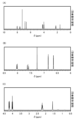

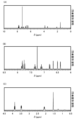


Classifications
-
- C—CHEMISTRY; METALLURGY
- C07—ORGANIC CHEMISTRY
- C07D—HETEROCYCLIC COMPOUNDS
- C07D487/00—Heterocyclic compounds containing nitrogen atoms as the only ring hetero atoms in the condensed system, not provided for by groups C07D451/00 - C07D477/00
- C07D487/02—Heterocyclic compounds containing nitrogen atoms as the only ring hetero atoms in the condensed system, not provided for by groups C07D451/00 - C07D477/00 in which the condensed system contains two hetero rings
- C07D487/04—Ortho-condensed systems
-
- H—ELECTRICITY
- H10—SEMICONDUCTOR DEVICES; ELECTRIC SOLID-STATE DEVICES NOT OTHERWISE PROVIDED FOR
- H10K—ORGANIC ELECTRIC SOLID-STATE DEVICES
- H10K50/00—Organic light-emitting devices
- H10K50/10—OLEDs or polymer light-emitting diodes [PLED]
- H10K50/17—Carrier injection layers
- H10K50/171—Electron injection layers
-
- H—ELECTRICITY
- H10—SEMICONDUCTOR DEVICES; ELECTRIC SOLID-STATE DEVICES NOT OTHERWISE PROVIDED FOR
- H10K—ORGANIC ELECTRIC SOLID-STATE DEVICES
- H10K85/00—Organic materials used in the body or electrodes of devices covered by this subclass
- H10K85/60—Organic compounds having low molecular weight
- H10K85/615—Polycyclic condensed aromatic hydrocarbons, e.g. anthracene
- H10K85/624—Polycyclic condensed aromatic hydrocarbons, e.g. anthracene containing six or more rings
-
- H—ELECTRICITY
- H10—SEMICONDUCTOR DEVICES; ELECTRIC SOLID-STATE DEVICES NOT OTHERWISE PROVIDED FOR
- H10K—ORGANIC ELECTRIC SOLID-STATE DEVICES
- H10K85/00—Organic materials used in the body or electrodes of devices covered by this subclass
- H10K85/60—Organic compounds having low molecular weight
- H10K85/615—Polycyclic condensed aromatic hydrocarbons, e.g. anthracene
- H10K85/626—Polycyclic condensed aromatic hydrocarbons, e.g. anthracene containing more than one polycyclic condensed aromatic rings, e.g. bis-anthracene
-
- H—ELECTRICITY
- H10—SEMICONDUCTOR DEVICES; ELECTRIC SOLID-STATE DEVICES NOT OTHERWISE PROVIDED FOR
- H10K—ORGANIC ELECTRIC SOLID-STATE DEVICES
- H10K85/00—Organic materials used in the body or electrodes of devices covered by this subclass
- H10K85/60—Organic compounds having low molecular weight
- H10K85/649—Aromatic compounds comprising a hetero atom
- H10K85/654—Aromatic compounds comprising a hetero atom comprising only nitrogen as heteroatom
-
- H—ELECTRICITY
- H10—SEMICONDUCTOR DEVICES; ELECTRIC SOLID-STATE DEVICES NOT OTHERWISE PROVIDED FOR
- H10K—ORGANIC ELECTRIC SOLID-STATE DEVICES
- H10K85/00—Organic materials used in the body or electrodes of devices covered by this subclass
- H10K85/60—Organic compounds having low molecular weight
- H10K85/649—Aromatic compounds comprising a hetero atom
- H10K85/657—Polycyclic condensed heteroaromatic hydrocarbons
- H10K85/6572—Polycyclic condensed heteroaromatic hydrocarbons comprising only nitrogen in the heteroaromatic polycondensed ring system, e.g. phenanthroline or carbazole
-
- H—ELECTRICITY
- H10—SEMICONDUCTOR DEVICES; ELECTRIC SOLID-STATE DEVICES NOT OTHERWISE PROVIDED FOR
- H10K—ORGANIC ELECTRIC SOLID-STATE DEVICES
- H10K50/00—Organic light-emitting devices
- H10K50/10—OLEDs or polymer light-emitting diodes [PLED]
- H10K50/14—Carrier transporting layers
- H10K50/16—Electron transporting layers
-
- H—ELECTRICITY
- H10—SEMICONDUCTOR DEVICES; ELECTRIC SOLID-STATE DEVICES NOT OTHERWISE PROVIDED FOR
- H10K—ORGANIC ELECTRIC SOLID-STATE DEVICES
- H10K50/00—Organic light-emitting devices
- H10K50/10—OLEDs or polymer light-emitting diodes [PLED]
- H10K50/19—Tandem OLEDs
Abstract
Description
本発明の一態様は、有機化合物、発光デバイス、発光装置、受発光装置、表示装置、電子機器、照明装置および電子デバイスに関する。なお、本発明の一態様は、上記の技術分野に限定されない。本明細書等で開示する発明の一態様の技術分野は、物、方法、または、製造方法に関するものである。または、本発明の一態様は、プロセス、マシン、マニュファクチャ、または、組成物(コンポジション・オブ・マター)に関するものである。そのため、より具体的に本明細書で開示する本発明の一態様の技術分野としては、半導体装置、表示装置、液晶表示装置、発光装置、照明装置、蓄電装置、記憶装置、撮像装置、それらの駆動方法、または、それらの製造方法、を一例として挙げることができる。 One embodiment of the present invention relates to an organic compound, a light-emitting device, a light-emitting device, a light receiving/emitting device, a display device, an electronic device, a lighting device, and an electronic device. Note that one embodiment of the present invention is not limited to the above technical field. The technical field of one embodiment of the invention disclosed in this specification and the like relates to products, methods, or manufacturing methods. Alternatively, one aspect of the present invention relates to a process, machine, manufacture, or composition of matter. Therefore, more specifically, the technical fields of one embodiment of the present invention disclosed in this specification include semiconductor devices, display devices, liquid crystal display devices, light-emitting devices, lighting devices, power storage devices, storage devices, imaging devices, and the like. Examples include driving methods and manufacturing methods thereof.
近年、表示装置は様々な用途への応用が期待されている。例えば、大型の表示装置の用途としては、家庭用のテレビジョン装置(テレビまたはテレビジョン受信機ともいう)、デジタルサイネージ(Digital Signage:電子看板)、及び、PID(Public Information Display)等が挙げられる。また、携帯情報端末として、タッチパネルを備えるスマートフォン及びタブレット端末などの開発が進められている。 In recent years, display devices are expected to be applied to various uses. For example, applications of large display devices include home television devices (also referred to as televisions or television receivers), digital signage (digital signage), PID (Public Information Display), etc. . Further, as mobile information terminals, smartphones and tablet terminals equipped with touch panels are being developed.
また、表示装置の高精細化が求められている。高精細な表示装置が要求される機器として、例えば、仮想現実(VR:Virtual Reality)、拡張現実(AR:Augmented Reality)、代替現実(SR:Substitutional Reality)、及び、複合現実(MR:Mixed Reality)向けの機器が、盛んに開発されている。 Furthermore, there is a demand for higher definition display devices. Examples of devices that require high-definition display devices include virtual reality (VR), augmented reality (AR), substitute reality (SR), and mixed reality (MR). ) devices are being actively developed.
表示装置としては、例えば、発光デバイス(発光素子ともいう)を有する発光装置が開発されている。エレクトロルミネッセンス(Electroluminescence、以下ELと記す)現象を利用した発光デバイス(ELデバイス、EL素子ともいう)は、薄型軽量化が容易である、入力信号に対し高速に応答可能である、直流定電圧電源を用いて駆動可能である等の特徴を有し、表示装置に応用されている。 As a display device, for example, a light-emitting device having a light-emitting device (also referred to as a light-emitting element) has been developed. A light emitting device (also referred to as an EL device or EL element) that utilizes the phenomenon of electroluminescence (hereinafter referred to as EL) is a DC constant voltage power supply that can be easily made thin and lightweight, and can respond quickly to input signals. It has characteristics such as being able to be driven using
特許文献1には、有機ELデバイス(有機EL素子ともいう)を用いた、VR向けの表示装置が開示されている。また、特許文献2には、遷移金属と非共有電子対を有する有機化合物の混合膜を電子注入層に用いた、駆動電圧が低く信頼性が良好な発光デバイスが開示されている。
有機半導体膜を所定の形状に作製する方法の一つとして、メタルマスクを用いた真空蒸着法(マスク蒸着)が広く用いられている。しかし、高密度化、高精細化が進む昨今、マスク蒸着は、合わせ精度の問題、基板との配置間隔の問題に代表される種々の理由により、これ以上の高精細化は限界に近付いている。一方、リソグラフィ法を用いて有機半導体膜の形状を加工することで、より緻密なパターンを形成することができる。この方法はさらに、大面積化も容易であることから、リソグラフィ法を用いた有機半導体膜の加工に関する研究も進められている。 As one method for manufacturing an organic semiconductor film into a predetermined shape, a vacuum evaporation method using a metal mask (mask evaporation) is widely used. However, as the density and definition of mask deposition continues to increase, mask deposition is approaching its limit due to various reasons such as alignment accuracy and spacing between substrates. . On the other hand, by processing the shape of an organic semiconductor film using a lithography method, a more precise pattern can be formed. Furthermore, since this method can be easily applied to a large area, research on processing organic semiconductor films using lithography is also progressing.
有機ELデバイスは、電極間(第1の電極と第2の電極との間)に発光物質を含む有機化合物層(上記有機半導体膜に相当)を有しており、電極から当該有機化合物層に注入されたキャリア(正孔および電子)を再結合させることによって生じたエネルギーによって、発光を得る構成を有している。 An organic EL device has an organic compound layer (corresponding to the above-mentioned organic semiconductor film) containing a light-emitting substance between the electrodes (between the first electrode and the second electrode), and the organic compound layer is formed from the electrode to the organic compound layer. It has a configuration in which light is emitted by energy generated by recombining injected carriers (holes and electrons).
ここで、有機化合物層は電気が流れにくくエネルギー障壁が大きいため、キャリアの注入、特に電子の注入には、基本的には高い電圧が必要であった。そのため、現状、陰極に接する電子注入層には、例えば仕事関数の小さいリチウム(Li)等のアルカリ金属または当該アルカリ金属の化合物が用いられ、低電圧化が実現されている。 Here, since it is difficult for electricity to flow through the organic compound layer and the energy barrier is large, a high voltage is basically required for injection of carriers, especially injection of electrons. Therefore, at present, for example, an alkali metal such as lithium (Li) having a small work function or a compound of the alkali metal is used for the electron injection layer in contact with the cathode, thereby realizing a low voltage.
しかし、上記アルカリ金属またはアルカリ金属化合物を含む有機半導体層を有する発光デバイスを、上述のリソグラフィ法を用いて作製する場合、大気中の酸素または水、工程中の薬液または水の影響により、駆動電圧の大幅な上昇または、電流効率の著しい低下を引き起こしてしまうという問題があった。 However, when producing a light-emitting device having an organic semiconductor layer containing the alkali metal or alkali metal compound using the above-mentioned lithography method, the drive voltage There has been a problem in that it causes a significant increase in current efficiency or a significant decrease in current efficiency.
この問題を解決する手段の一つとして、発光デバイスの有機化合物層を形成する途中で(アルカリ金属またはアルカリ金属化合物を含む層を形成する前に)リソグラフィ法を用いて加工する工程を行う方法がある。すなわち、電子注入層を形成する前の段階でリソグラフィを行って有機化合物層を加工し、その後に電子注入層の形成工程およびその後の工程を行うことにより特性の悪化を回避することができる。 One way to solve this problem is to perform a processing process using lithography during the formation of the organic compound layer of the light emitting device (before forming the layer containing the alkali metal or alkali metal compound). be. That is, deterioration of the characteristics can be avoided by performing lithography to process the organic compound layer before forming the electron injection layer, and then performing the step of forming the electron injection layer and the subsequent steps.
しかし、タンデム型の発光デバイスでは上述の回避方法を適用することができず、リソグラフィ法を用いて有機化合物層を加工する工程を行ったことに起因する大幅な特性の悪化が避けられなかった。 However, the above-described avoidance method cannot be applied to tandem-type light emitting devices, and a significant deterioration in characteristics due to the step of processing the organic compound layer using lithography cannot be avoided.
なぜならば、タンデム型の発光デバイスは、中間層を挟んで複数の発光層が直列に積層された構造の有機半導体層を有しており、当該中間層には、陽極側の発光層に電子を注入するために、アルカリ金属またはアルカリ金属化合物を含む層が含まれるからである。中間層は2つの発光層の間に存在することから、2つの発光層を含む有機化合物層をリソグラフィ法によって加工しようとすれば、必ず中間層もリソグラフィ法を用いて加工することとなり、酸素、水などに曝されることになる。 This is because a tandem light emitting device has an organic semiconductor layer with a structure in which multiple light emitting layers are stacked in series with an intermediate layer in between, and the intermediate layer has a structure in which electrons are transferred to the light emitting layer on the anode side. This is because a layer containing an alkali metal or an alkali metal compound is included for implantation. Since the intermediate layer exists between two light-emitting layers, if an organic compound layer containing two light-emitting layers is to be processed using lithography, the intermediate layer must also be processed using lithography. It will be exposed to water etc.
そのため、中間層におけるアルカリ金属またはアルカリ金属化合物を含む層をリソグラフィ法によって加工することによって、電子注入層をリソグラフィ法によって加工した場合と同様に、発光デバイスの駆動電圧の大幅な上昇、および電流効率の著しい低下が引き起こされてしまっていた。 Therefore, by processing the layer containing an alkali metal or alkali metal compound in the intermediate layer by lithography, it is possible to significantly increase the driving voltage and current efficiency of the light emitting device, similar to when processing the electron injection layer by lithography. This resulted in a significant decrease in
また、上述の問題を解決する別の手段として、アルカリ金属またはアルカリ金属化合物の代わりに、電子注入性を有する有機化合物を、電子注入層または中間層に用いる方法がある。すなわち、この方法では、アルカリ金属またはアルカリ金属化合物を含まない有機化合物層をリソグラフィ法によって加工するため、アルカリ金属または当該アルカリ金属の化合物に起因する発光デバイスの特性の悪化を回避することができる。 Further, as another means for solving the above-mentioned problem, there is a method of using an organic compound having electron injection properties in the electron injection layer or intermediate layer instead of the alkali metal or alkali metal compound. That is, in this method, since an organic compound layer that does not contain an alkali metal or an alkali metal compound is processed by a lithography method, it is possible to avoid deterioration of the characteristics of the light emitting device due to the alkali metal or the compound of the alkali metal.
しかし、当該有機化合物の水への溶解性が高いと、水、または水を溶媒とする薬液に曝される工程において当該有機化合物を用いた層が溶解することで、特性の低下、形状不良などの原因となる場合があった。 However, if the organic compound has high solubility in water, the layer using the organic compound will dissolve during the process of being exposed to water or a chemical solution using water as a solvent, resulting in decreased properties, poor shape, etc. It could be the cause of.
また、本発明の一態様は、電子注入性を有する有機化合物を提供することを課題とする。また、本発明の一態様は、水への溶解性の低い有機化合物を提供することを課題とする。また、本発明の一態様は、良好な特性の発光デバイスを提供することを課題とする。また、本発明の一態様は、新規な有機化合物、新規な発光デバイス、新規な発光装置、または新規な電子機器を提供することを課題とする。 Further, it is an object of one embodiment of the present invention to provide an organic compound having electron injection properties. Another object of one embodiment of the present invention is to provide an organic compound with low solubility in water. Another object of one embodiment of the present invention is to provide a light-emitting device with good characteristics. Another object of one embodiment of the present invention is to provide a novel organic compound, a novel light-emitting device, a novel light-emitting device, or a new electronic device.
なお、これらの課題の記載は、他の課題の存在を妨げるものではない。本発明の一態様は、必ずしも、これらの課題の全てを解決する必要はないものとする。明細書、図面、請求項の記載から、これら以外の課題を抽出することが可能である。 Note that the description of these issues does not preclude the existence of other issues. One embodiment of the present invention does not necessarily need to solve all of these problems. Problems other than these can be extracted from the description, drawings, and claims.
本発明の一態様では、上述の問題を解決するため、環状グアニジン骨格と、芳香族炭化水素骨格または複素芳香族炭化水素骨格と、を有する有機化合物を提供する。このような有機化合物は、電子注入性を有し、電子注入層または中間層において、アルカリ金属またはアルカリ金属化合物の代わりに用いることができる。なお、環状グアニジン骨格は、イミダゾール環を含むことが好ましい。イミダゾール環を含む環状グアニジン骨格とすることにより、水への溶解性が低く、リソグラフィ法による加工の工程において層が溶解することを回避することができる。従って、本発明の一態様の有機化合物を電子注入層または中間層においてアルカリ金属またはアルカリ金属化合物の代わりに用いることにより、アルカリ金属または当該アルカリ金属の化合物に起因する特性の悪化を回避し、良好な特性の発光デバイスを得ることができる。 In one aspect of the present invention, in order to solve the above problems, an organic compound having a cyclic guanidine skeleton and an aromatic hydrocarbon skeleton or a heteroaromatic hydrocarbon skeleton is provided. Such organic compounds have electron injection properties and can be used in place of alkali metals or alkali metal compounds in the electron injection layer or intermediate layer. Note that the cyclic guanidine skeleton preferably includes an imidazole ring. By using a cyclic guanidine skeleton containing an imidazole ring, the solubility in water is low, and it is possible to avoid dissolution of the layer during the processing process using the lithography method. Therefore, by using the organic compound of one embodiment of the present invention in place of the alkali metal or alkali metal compound in the electron injection layer or the intermediate layer, deterioration of the characteristics caused by the alkali metal or the alkali metal compound can be avoided and the properties can be improved. A light emitting device with excellent characteristics can be obtained.
すなわち、本発明の一態様は、下記一般式(G1)で表される有機化合物である。 That is, one embodiment of the present invention is an organic compound represented by the following general formula (G1).
ただし、上記一般式(G1)で表される有機化合物において、Arは置換もしくは無置換の環を形成する炭素の数が6乃至30の芳香族炭化水素基、または、置換もしくは無置換の環を形成する炭素の数が2乃至30の複素芳香族炭化水素基を表し、R1およびR2はそれぞれ独立に水素(重水素を含む)、炭素数1乃至6のアルキル基、置換もしくは無置換のアミノ基、置換もしくは無置換の環を形成する炭素の数が6乃至13のアリール基、または置換もしくは無置換の環を形成する炭素の数が2乃至13のヘテロアリール基を表し、nは1乃至6の整数を表し、Lは上記一般式(L-1)で表される基である。また、上記一般式(L-1)において、R3およびR4はそれぞれ独立に水素(重水素を含む)、または炭素数1乃至6のアルキル基を表し、kは1乃至5の整数を表し、kが2以上の場合、それぞれのR3およびR4は同じであっても異なっていてもよい。 However, in the organic compound represented by the above general formula (G1), Ar represents an aromatic hydrocarbon group having 6 to 30 carbon atoms forming a substituted or unsubstituted ring, or a substituted or unsubstituted ring. Represents a heteroaromatic hydrocarbon group having 2 to 30 carbon atoms, and R 1 and R 2 each independently represent hydrogen (including deuterium), an alkyl group having 1 to 6 carbon atoms, or a substituted or unsubstituted represents an amino group, an aryl group having 6 to 13 carbon atoms forming a substituted or unsubstituted ring, or a heteroaryl group having 2 to 13 carbon atoms forming a substituted or unsubstituted ring, where n is 1 It represents an integer of 6 to 6, and L is a group represented by the above general formula (L-1). Furthermore, in the above general formula (L-1), R 3 and R 4 each independently represent hydrogen (including deuterium) or an alkyl group having 1 to 6 carbon atoms, and k represents an integer of 1 to 5. , k is 2 or more, each R 3 and R 4 may be the same or different.
また、本発明の一態様は、下記一般式(G2-1)乃至(G2-3)のいずれかで表される有機化合物である。 Further, one embodiment of the present invention is an organic compound represented by any of the following general formulas (G2-1) to (G2-3).
ただし、上記一般式(G2-1)乃至一般式(G2-3)で表される有機化合物において、Arは置換もしくは無置換の環を形成する炭素の数が6乃至30の芳香族炭化水素基、または、置換もしくは無置換の環を形成する炭素の数が2乃至30の複素芳香族炭化水素基を表し、R1、R2およびR11乃至R28はそれぞれ独立に水素(重水素を含む)、または炭素数1乃至6のアルキル基を表し、nは1乃至6の整数を表す。 However, in the organic compounds represented by the above general formulas (G2-1) to (G2-3), Ar is an aromatic hydrocarbon group having 6 to 30 carbon atoms forming a substituted or unsubstituted ring. , or represents a heteroaromatic hydrocarbon group having 2 to 30 carbon atoms forming a substituted or unsubstituted ring, and R 1 , R 2 and R 11 to R 28 are each independently hydrogen (including deuterium). ), or an alkyl group having 1 to 6 carbon atoms, and n represents an integer of 1 to 6.
また、本発明の一態様は、上記各構成において、環を形成する炭素の数が6乃至30の芳香族炭化水素基および環を形成する炭素の数が2乃至30の複素芳香族炭化水素基は、下記構造式(Ar-1)乃至(Ar-27)のいずれかで表される芳香族炭化水素および複素芳香族炭化水素のいずれか一の環からn個の水素原子を除いた構造を有する基である、有機化合物である。 Further, in each of the above structures, one aspect of the present invention provides an aromatic hydrocarbon group having 6 to 30 carbon atoms forming a ring and a heteroaromatic hydrocarbon group having 2 to 30 carbon atoms forming a ring. is a structure in which n hydrogen atoms are removed from the ring of any one of aromatic hydrocarbons and heteroaromatic hydrocarbons represented by any of the following structural formulas (Ar-1) to (Ar-27). It is an organic compound that has a group that has
また、本発明の一態様は、下記構造式(100)、(101)または(113)で表される有機化合物である。 Further, one embodiment of the present invention is an organic compound represented by the following structural formula (100), (101), or (113).
また、本発明の一態様は、上記各構成の有機化合物を用いた発光デバイスである。 Further, one embodiment of the present invention is a light-emitting device using an organic compound having each of the above structures.
また、本発明の一態様は、上記構成の発光デバイスと、トランジスタ、または、基板と、を有する発光装置である。 Further, one embodiment of the present invention is a light-emitting device including a light-emitting device having the above structure, a transistor, or a substrate.
また、本発明の一態様は、上記構成の発光装置と、検知部、入力部、または、通信部と、を有する電子機器である。 Further, one embodiment of the present invention is an electronic device including the light emitting device having the above structure, and a detection section, an input section, or a communication section.
なお、本明細書中における発光装置とは、発光デバイスを用いた画像表示デバイスを含む。また、基板上の発光デバイスにコネクター、例えば異方導電性フィルム又はTCP(Tape Carrier Package)が取り付けられたモジュール、TCPの先にプリント配線板が設けられたモジュール、又は発光デバイスにCOG(Chip On Glass)方式によりIC(集積回路)が直接実装されたモジュールも発光装置に含む場合がある。さらに、照明器具等は、発光装置を有する場合がある。 Note that the light-emitting device in this specification includes an image display device using a light-emitting device. In addition, a module in which a connector such as an anisotropic conductive film or TCP (Tape Carrier Package) is attached to a light emitting device on a substrate, a module in which a printed wiring board is provided at the end of TCP, or a COG (Chip On The light emitting device may also include a module in which an IC (integrated circuit) is directly mounted using the glass method. Furthermore, lighting equipment and the like may include a light emitting device.
本発明の一態様により、電子注入性を有する有機化合物を提供することができる。また、本発明の一態様により、水への溶解性の低い有機化合物を提供することができる。また、本発明の一態様により、良好な特性の発光デバイスを提供することができる。また、本発明の一態様により、新規な有機化合物または新規な発光デバイスを提供することができる。 According to one embodiment of the present invention, an organic compound having electron injection properties can be provided. Further, according to one embodiment of the present invention, an organic compound with low solubility in water can be provided. Further, according to one embodiment of the present invention, a light-emitting device with good characteristics can be provided. Further, according to one embodiment of the present invention, a novel organic compound or a novel light-emitting device can be provided.
本発明の一態様により、表示品位の高い発光装置を提供することができる。または、本発明の一態様により、高精細な発光装置を提供することができる。または、本発明の一態様により、高解像度の発光装置を提供することができる。または、本発明の一態様により、信頼性の高い発光装置を提供することができる。または、本発明の一態様により、利便性、有用性または信頼性に優れた新規な発光装置を提供することができる。または、本発明の一態様により、利便性、有用性または信頼性に優れた新規な表示モジュールを提供することができる。または、本発明の一態様により、利便性、有用性または信頼性に優れた新規な電子機器を提供することができる。または、本発明の一態様により、新規な発光装置、新規な表示モジュール、新規な電子機器または新規な半導体装置を提供することができる。 According to one embodiment of the present invention, a light-emitting device with high display quality can be provided. Alternatively, according to one embodiment of the present invention, a high-definition light-emitting device can be provided. Alternatively, according to one embodiment of the present invention, a high-resolution light-emitting device can be provided. Alternatively, according to one embodiment of the present invention, a highly reliable light-emitting device can be provided. Alternatively, according to one embodiment of the present invention, a novel light-emitting device that is highly convenient, useful, or reliable can be provided. Alternatively, according to one embodiment of the present invention, a novel display module that is highly convenient, useful, or reliable can be provided. Alternatively, according to one embodiment of the present invention, a novel electronic device with excellent convenience, usefulness, or reliability can be provided. Alternatively, according to one embodiment of the present invention, a new light emitting device, a new display module, a new electronic device, or a new semiconductor device can be provided.
なお、これらの効果の記載は、他の効果の存在を妨げるものではない。本発明の一態様は、必ずしも、これらの効果の全てを有する必要はない。明細書、図面、請求項の記載から、これら以外の効果を抽出することが可能である。 Note that the description of these effects does not preclude the existence of other effects. One embodiment of the present invention does not necessarily need to have all of these effects. Effects other than these can be extracted from the description, drawings, and claims.
実施の形態について、図面を用いて詳細に説明する。但し、本発明は以下の説明に限定されず、本発明の趣旨及びその範囲から逸脱することなくその形態及び詳細を様々に変更し得ることは当業者であれば容易に理解される。従って、本発明は以下に示す実施の形態の記載内容に限定して解釈されるものではない。 Embodiments will be described in detail using the drawings. However, those skilled in the art will easily understand that the present invention is not limited to the following description, and that the form and details thereof can be changed in various ways without departing from the spirit and scope of the present invention. Therefore, the present invention should not be interpreted as being limited to the contents described in the embodiments shown below.
なお、以下に説明する発明の構成において、同一部分又は同様な機能を有する部分には同一の符号を異なる図面間で共通して用い、その繰り返しの説明は省略する。また、同様の機能を指す場合には、ハッチパターンを同じくし、特に符号を付さない場合がある。 In the configuration of the invention described below, the same parts or parts having similar functions are designated by the same reference numerals in different drawings, and repeated explanation thereof will be omitted. Furthermore, when referring to similar functions, the same hatch pattern may be used and no particular reference numeral may be attached.
また、図面において示す各構成の、位置、大きさ、及び、範囲などは、理解の簡単のため、実際の位置、大きさ、及び、範囲などを表していない場合がある。このため、開示する発明は、必ずしも、図面に開示された位置、大きさ、及び、範囲などに限定されない。 Further, for ease of understanding, the position, size, range, etc. of each structure shown in the drawings may not represent the actual position, size, range, etc. Therefore, the disclosed invention is not necessarily limited to the position, size, range, etc. disclosed in the drawings.
なお、「膜」という言葉と、「層」という言葉とは、場合によっては、または、状況に応じて、互いに入れ替えることが可能である。例えば、「導電層」という用語を、「導電膜」という用語に変更することが可能である。または、例えば、「絶縁膜」という用語を、「絶縁層」という用語に変更することが可能である。 Note that the words "film" and "layer" can be interchanged depending on the situation or circumstances. For example, the term "conductive layer" can be changed to the term "conductive film." Alternatively, for example, the term "insulating film" can be changed to the term "insulating layer."
なお、本明細書等において、メタルマスク、またはFMM(ファインメタルマスク、高精細なメタルマスク)を用いて作製されるデバイスをMM(メタルマスク)構造のデバイスと呼称する場合がある。また、本明細書等において、メタルマスク、またはFMMを用いることなく作製されるデバイスをMML(メタルマスクレス)構造のデバイスと呼称する場合がある。 Note that in this specification and the like, a device manufactured using a metal mask or an FMM (fine metal mask, high-definition metal mask) is sometimes referred to as a device with an MM (metal mask) structure. Further, in this specification and the like, a device manufactured without using a metal mask or FMM may be referred to as a device with an MML (metal maskless) structure.
本明細書等において、正孔または電子を、「キャリア」といって示す場合がある。具体的には、正孔注入層または電子注入層を「キャリア注入層」といい、正孔輸送層または電子輸送層を「キャリア輸送層」といい、正孔ブロック層または電子ブロック層を「キャリアブロック層」という場合がある。なお、上述のキャリア注入層、キャリア輸送層、及びキャリアブロック層は、それぞれ、断面形状、または特性などによって明確に区別できない場合がある。また、1つの層が、キャリア注入層、キャリア輸送層、及びキャリアブロック層のうち2つまたは3つの機能を兼ねる場合がある。 In this specification, holes or electrons may be referred to as "carriers." Specifically, a hole injection layer or an electron injection layer is called a "carrier injection layer," a hole transport layer or an electron transport layer is called a "carrier transport layer," and a hole blocking layer or an electron blocking layer is called a "carrier injection layer." Sometimes called the "block layer". Note that the carrier injection layer, carrier transport layer, and carrier block layer described above may not be clearly distinguishable depending on their respective cross-sectional shapes or characteristics. Moreover, one layer may serve as two or three functions among a carrier injection layer, a carrier transport layer, and a carrier block layer.
本明細書等において、発光デバイス(発光素子ともいう)は、一対の電極間にEL層を有する。EL層は、少なくとも発光層を有する。本明細書等において、受光デバイス(受光素子ともいう)は、一対の電極間に少なくとも光電変換層として機能する活性層を有する。本明細書等では、一対の電極の一方を画素電極と記し、他方を共通電極と記すことがある。 In this specification and the like, a light emitting device (also referred to as a light emitting element) has an EL layer between a pair of electrodes. The EL layer has at least a light emitting layer. In this specification and the like, a light-receiving device (also referred to as a light-receiving element) has an active layer that functions as at least a photoelectric conversion layer between a pair of electrodes. In this specification and the like, one of a pair of electrodes is sometimes referred to as a pixel electrode, and the other is sometimes referred to as a common electrode.
なお、本明細書等において、テーパ形状とは、構造の側面の少なくとも一部が、基板面に対して傾斜して設けられている形状のことを指す。例えば、傾斜した側面と基板面とがなす角(テーパ角ともいう)が90°未満である領域を有すると好ましい。なお、構造の側面及び基板面は、必ずしも完全に平坦である必要はなく、微細な曲率を有する略平面状、または微細な凹凸を有する略平面状であってもよい。 Note that in this specification and the like, the term "tapered shape" refers to a shape in which at least a part of the side surface of the structure is inclined with respect to the substrate surface. For example, it is preferable to have a region where the angle between the inclined side surface and the substrate surface (also referred to as a taper angle) is less than 90°. Note that the side surfaces of the structure and the substrate surface do not necessarily have to be completely flat, and may be substantially planar with minute curvatures or substantially planar with minute irregularities.
なお、本明細書中における発光装置とは、有機ELデバイスを用いた画像表示デバイスを含む。また、有機ELデバイスにコネクター、例えば異方導電性フィルム又はTCP(Tape Carrier Package)が取り付けられたモジュール、TCPの先にプリント配線板が設けられたモジュール、又は有機ELデバイスにCOG(Chip On Glass)方式によりIC(集積回路)が直接実装されたモジュールも発光装置に含む場合がある。さらに、照明器具等は、発光装置を有する場合がある。 Note that the light emitting device in this specification includes an image display device using an organic EL device. In addition, a module in which a connector such as an anisotropic conductive film or TCP (Tape Carrier Package) is attached to an organic EL device, a module in which a printed wiring board is provided at the end of the TCP, or a COG (Chip On Glass) to an organic EL device. The light emitting device may also include a module in which an IC (integrated circuit) is directly mounted using the ) method. Furthermore, lighting equipment and the like may include a light emitting device.
(実施の形態1)
本実施の形態では、本発明の一態様の有機化合物について説明する。
(Embodiment 1)
In this embodiment, an organic compound of one embodiment of the present invention will be described.
上述の通り、本発明の一態様では、課題解決のため、環状グアニジン骨格と、芳香族炭化水素骨格または複素芳香族炭化水素骨格と、を有する有機化合物を提供する。このような有機化合物は、電子注入性を有し、電子注入層または中間層において、アルカリ金属またはアルカリ金属化合物の代わりに用いることができる。なお、環状グアニジン骨格は、イミダゾール環を含むことが好ましい。イミダゾール環を含む環状グアニジン骨格とすることにより、水への溶解性が低く、リソグラフィ法による加工の工程において層が溶解することを回避することができる。従って、本発明の一態様の有機化合物を電子注入層または中間層においてアルカリ金属またはアルカリ金属化合物の代わりに用いることにより、アルカリ金属または当該アルカリ金属の化合物に起因する特性の悪化を回避し、良好な特性の発光デバイスを得ることができる。 As described above, in order to solve the problem, one aspect of the present invention provides an organic compound having a cyclic guanidine skeleton and an aromatic hydrocarbon skeleton or a heteroaromatic hydrocarbon skeleton. Such organic compounds have electron injection properties and can be used in place of alkali metals or alkali metal compounds in the electron injection layer or intermediate layer. Note that the cyclic guanidine skeleton preferably includes an imidazole ring. By using a cyclic guanidine skeleton containing an imidazole ring, the solubility in water is low, and it is possible to avoid dissolution of the layer during the processing process using the lithography method. Therefore, by using the organic compound of one embodiment of the present invention in place of the alkali metal or alkali metal compound in the electron injection layer or the intermediate layer, deterioration of the characteristics caused by the alkali metal or the alkali metal compound can be avoided and the properties can be improved. A light emitting device with excellent characteristics can be obtained.
すなわち、本発明の一態様は、下記一般式(G1)で表される有機化合物である。 That is, one embodiment of the present invention is an organic compound represented by the following general formula (G1).
ただし、上記一般式(G1)で表される有機化合物において、Arは置換もしくは無置換の環を形成する炭素の数が6乃至30の芳香族炭化水素基、または、置換もしくは無置換の環を形成する炭素の数が2乃至30の複素芳香族炭化水素基を表し、R1およびR2はそれぞれ独立に水素(重水素を含む)、炭素数1乃至6のアルキル基、置換もしくは無置換のアミノ基、置換もしくは無置換の環を形成する炭素の数が6乃至13のアリール基、または置換もしくは無置換の環を形成する炭素の数が2乃至13のヘテロアリール基を表し、nは1乃至6の整数を表し、Lは上記一般式(L-1)で表される基である。また、上記一般式(L-1)において、R3およびR4はそれぞれ独立に水素(重水素を含む)、または炭素数1乃至6のアルキル基を表し、kは1乃至5の整数を表し、kが2以上の場合、それぞれのR3およびR4は同じであっても異なっていてもよい。 However, in the organic compound represented by the above general formula (G1), Ar represents an aromatic hydrocarbon group having 6 to 30 carbon atoms forming a substituted or unsubstituted ring, or a substituted or unsubstituted ring. Represents a heteroaromatic hydrocarbon group having 2 to 30 carbon atoms, and R 1 and R 2 each independently represent hydrogen (including deuterium), an alkyl group having 1 to 6 carbon atoms, or a substituted or unsubstituted represents an amino group, an aryl group having 6 to 13 carbon atoms forming a substituted or unsubstituted ring, or a heteroaryl group having 2 to 13 carbon atoms forming a substituted or unsubstituted ring, where n is 1 It represents an integer of 6 to 6, and L is a group represented by the above general formula (L-1). Furthermore, in the above general formula (L-1), R 3 and R 4 each independently represent hydrogen (including deuterium) or an alkyl group having 1 to 6 carbon atoms, and k represents an integer of 1 to 5. , k is 2 or more, each R 3 and R 4 may be the same or different.
このように、環状グアニジン骨格を有する構造とすることにより、有機化合物に電子注入性を持たせることができる。また環状グアニジン骨格がイミダゾール環を含むことによって、水への溶解性を低くすることができる。従って、このような構造の有機化合物を電子注入層または中間層に用いることにより、良好な特性の発光デバイスを得ることができる。 In this way, by forming the structure having a cyclic guanidine skeleton, the organic compound can be given electron injection properties. Furthermore, since the cyclic guanidine skeleton contains an imidazole ring, the solubility in water can be lowered. Therefore, by using an organic compound having such a structure in the electron injection layer or intermediate layer, a light emitting device with good characteristics can be obtained.
また、本発明の一態様は、下記一般式(G2-1)乃至(G2-3)のいずれかで表される有機化合物である。 Further, one embodiment of the present invention is an organic compound represented by any of the following general formulas (G2-1) to (G2-3).
ただし、上記一般式(G2-1)乃至一般式(G2-3)で表される有機化合物において、Arは置換もしくは無置換の環を形成する炭素の数が6乃至30の芳香族炭化水素基、または、置換もしくは無置換の環を形成する炭素の数が2乃至30の複素芳香族炭化水素基を表し、R1、R2およびR11乃至R28はそれぞれ独立に水素(重水素を含む)、または炭素数1乃至6のアルキル基を表し、nは1乃至6の整数を表す。 However, in the organic compounds represented by the above general formulas (G2-1) to (G2-3), Ar is an aromatic hydrocarbon group having 6 to 30 carbon atoms forming a substituted or unsubstituted ring. , or represents a heteroaromatic hydrocarbon group having 2 to 30 carbon atoms forming a substituted or unsubstituted ring, and R 1 , R 2 and R 11 to R 28 are each independently hydrogen (including deuterium). ), or an alkyl group having 1 to 6 carbon atoms, and n represents an integer of 1 to 6.
上記一般式(G2-1)乃至一般式(G2-3)で表される有機化合物は、上記一般式(G1)で表される有機化合物におけるkを2乃至4の整数と限定した構造を有する。このような構造とすると、環状グアニジン骨格の安定性を高めることができるため、有機化合物全体の安定を高めることができ、好ましい。 The organic compounds represented by the above general formula (G2-1) to general formula (G2-3) have a structure in which k in the organic compound represented by the above general formula (G1) is limited to an integer of 2 to 4. . Such a structure is preferable because it can increase the stability of the cyclic guanidine skeleton, thereby increasing the stability of the organic compound as a whole.
なお、上記一般式(G1)および一般式(G2-1)乃至(G2-3)において、nは、1乃至4の整数であることがより好ましく、1または2であることがさらに好ましい。これによって当該有機化合物の水、または水を溶媒とする薬液に対する溶解性を低下させることができる。 In addition, in the above general formula (G1) and general formulas (G2-1) to (G2-3), n is more preferably an integer of 1 to 4, and even more preferably 1 or 2. This can reduce the solubility of the organic compound in water or a chemical solution using water as a solvent.
《芳香族炭化水素および複素芳香族炭化水素の具体例》
また、上記一般式(G1)および一般式(G2-1)乃至(G2-3)で表される有機化合物において、環を形成する炭素の数が6乃至30の芳香族炭化水素基とは、環を形成する炭素の数が6乃至30の芳香族炭化水素からn個の水素原子を除いた構造を有する基であり、環を形成する炭素の数が2乃至30の複素芳香族炭化水素基とは、環を形成する炭素の数が2乃至30の複素芳香族炭化水素からn個の水素原子を除いた構造を有する基である。
《Specific examples of aromatic hydrocarbons and heteroaromatic hydrocarbons》
In addition, in the organic compounds represented by the above general formula (G1) and general formulas (G2-1) to (G2-3), an aromatic hydrocarbon group having 6 to 30 carbon atoms forming a ring, A group having a structure in which n hydrogen atoms are removed from an aromatic hydrocarbon having 6 to 30 carbon atoms forming a ring, and a heteroaromatic hydrocarbon group having 2 to 30 carbon atoms forming a ring. is a group having a structure obtained by removing n hydrogen atoms from a heteroaromatic hydrocarbon having 2 to 30 carbon atoms forming a ring.
上記一般式(G1)および一般式(G2-1)乃至(G2-3)で表される有機化合物において、n個の水素原子を除くことによって、環を形成する炭素の数が6乃至30の芳香族炭化水素基として用いることのできる環を形成する炭素の数が6乃至30の芳香族炭化水素の具体例としては、ベンゼン、ナフタレン、フルオレン、スピロビフルオレン、アントラセン、フェナントレン、トリフェニレン、ピレン、テトラセン、クリセン、ベンズ(a)アントラセンなどを挙げることができる。ただし、環を形成する炭素の数が6乃至30の芳香族炭化水素基の具体例はこれに限定されない。 In the organic compounds represented by the above general formula (G1) and general formulas (G2-1) to (G2-3), by removing n hydrogen atoms, the number of carbon atoms forming the ring is increased from 6 to 30. Specific examples of aromatic hydrocarbons having 6 to 30 carbon atoms forming a ring that can be used as aromatic hydrocarbon groups include benzene, naphthalene, fluorene, spirobifluorene, anthracene, phenanthrene, triphenylene, pyrene, Examples include tetracene, chrysene, benz(a)anthracene, and the like. However, specific examples of the aromatic hydrocarbon group having 6 to 30 carbon atoms forming a ring are not limited thereto.
上記一般式(G1)および一般式(G2-1)乃至(G2-3)で表される有機化合物において、n個の水素原子を除くことによって、環を形成する炭素の数が2乃至30の複素芳香族炭化水素基として用いることのできる、環を形成する炭素の数が2乃至30の複素芳香族炭化水素の具体例としては、ピリジン、ビピリジン、ピリミジン、ビピリミジン、ピラジン、ビピラジン、トリアジン、キノリン、イソキノリン、ベンゾキノリン、フェナントロリン、キノキサリン、ベンゾキノキサリン、ジベンゾキノキサリン、アザフルオレン、ジアザフルオレン、カルバゾール、ベンゾカルバゾ-ル、ジベンゾカルバゾ-ル、ジベンゾフラン、ベンゾナフトフラン、ジナフトフラン、ジベンゾチオフェン、ベンゾナフトチオフェン、ジナフトチオフェン、ベンゾフロピリジン、ベンゾフロピリミジン、ベンゾチオピリジン、ベンゾチオピリミジン、ナフトフロピリジン、ナフトフロピリミジン、ナフトチオピリジン、ナフトチオピリミジン、アクリジン、キサンテン、フェノチアジン、フェノキサジン、フェナジン、トリアゾ-ル、オキサゾ-ル、オキサジアゾール、チアゾ-ル、チアジアゾ-ル、イミダゾ-ル、ベンゾイミダゾール、ピラゾ-ル、ピロ-ルなどを挙げることができる。ただし、環を形成する炭素の数が2乃至30の複素芳香族炭化水素の具体例はこれに限定されない。 In the organic compounds represented by the above general formula (G1) and general formulas (G2-1) to (G2-3), the number of carbon atoms forming the ring can be increased from 2 to 30 by removing n hydrogen atoms. Specific examples of heteroaromatic hydrocarbons having a ring having 2 to 30 carbon atoms that can be used as the heteroaromatic hydrocarbon group include pyridine, bipyridine, pyrimidine, bipyrimidine, pyrazine, bipyrazine, triazine, and quinoline. , isoquinoline, benzoquinoline, phenanthroline, quinoxaline, benzoquinoxaline, dibenzoquinoxaline, azafluorene, diazafluorene, carbazole, benzocarbazole, dibenzocarbazole, dibenzofuran, benzonaphthofuran, dinaphthofuran, dibenzothiophene, benzonaphthothiophene, Dinaphthothiophene, benzofuropyridine, benzofuropyrimidine, benzothiopyridine, benzothiopyrimidine, naphthofuropyridine, naphthofuropyrimidine, naphthothiopyridine, naphthothiopyrimidine, acridine, xanthene, phenothiazine, phenoxazine, phenazine, triazole , oxazole, oxadiazole, thiazole, thiadiazole, imidazole, benzimidazole, pyrazole, pyrrole and the like. However, specific examples of heteroaromatic hydrocarbons having 2 to 30 carbon atoms forming a ring are not limited thereto.
上記一般式(G1)および一般式(G2-1)乃至(G2-3)で表される有機化合物においてn個の水素原子を除くことによって、環を形成する炭素の数が6乃至30の芳香族炭化水素基または環を形成する炭素の数が2乃至30の複素芳香族炭化水素基として用いることのできる、環を形成する炭素の数が6乃至30の芳香族炭化水素および環を形成する炭素の数が2乃至30の複素芳香族炭化水素の具体例として、上記した中でも、下記構造式(Ar-1)乃至(Ar-27)のいずれか一であることがより好ましい。 By removing n hydrogen atoms from the organic compounds represented by the above general formula (G1) and general formulas (G2-1) to (G2-3), aromatic compounds having 6 to 30 carbon atoms forming a ring can be obtained. An aromatic hydrocarbon having 6 to 30 carbon atoms forming a ring and an aromatic hydrocarbon group having 6 to 30 carbon atoms forming a ring, which can be used as a group hydrocarbon group or a heteroaromatic hydrocarbon group having 2 to 30 carbon atoms forming a ring. Among the above-mentioned examples of the heteroaromatic hydrocarbon having 2 to 30 carbon atoms, any one of the following structural formulas (Ar-1) to (Ar-27) is more preferable.
また、上記した環を形成する炭素の数が6乃至30の芳香族炭化水素および環を形成する炭素の数が2乃至30の複素芳香族炭化水素の中で、上記構造式(Ar-5)または構造式(Ar-20)からn個の水素を除いた構造を有する基をArとして用いるとさらに好ましい。これらの芳香族炭化水素または複素芳香族炭化水素を用いることにより、水、または水を溶媒とする薬液に対する溶解性を低下させることができる。 Furthermore, among the aromatic hydrocarbons having 6 to 30 carbon atoms forming a ring and the heteroaromatic hydrocarbons having 2 to 30 carbon atoms forming a ring, the above structural formula (Ar-5) Alternatively, it is more preferable to use a group having a structure obtained by removing n hydrogens from structural formula (Ar-20) as Ar. By using these aromatic hydrocarbons or heteroaromatic hydrocarbons, the solubility in water or a chemical solution using water as a solvent can be reduced.
なお、環を形成する炭素の数が2乃至30の複素芳香族炭化水素が、環を構成する元素として窒素を含む場合、当該窒素または当該窒素に隣接する炭素と、環状グアニジン骨格と、が結合することがより好ましい。これによって、有機化合物の電子注入性を高めることができる。 In addition, when a heteroaromatic hydrocarbon having 2 to 30 carbon atoms forming a ring contains nitrogen as an element forming the ring, the nitrogen or the carbon adjacent to the nitrogen and the cyclic guanidine skeleton are bonded. It is more preferable to do so. Thereby, the electron injection property of the organic compound can be improved.
なお、環を形成する炭素の数が6乃至30の芳香族炭化水素基、または、置換もしくは無置換の環を形成する炭素の数が2乃至30の複素芳香族炭化水素基が置換基を有する場合、当該置換基の具体例としては、炭素数1乃至6のアルキル基、炭素数6乃至13のアリール基、炭素数2乃至13のヘテロアリール基などが挙げられる。また、環を形成する炭素の数が6乃至30の芳香族炭化水素基、または、置換もしくは無置換の環を形成する炭素の数が2乃至30の複素芳香族炭化水素基の有する水素の一部または全てが重水素であってもよい。 In addition, an aromatic hydrocarbon group having 6 to 30 carbon atoms forming a ring, or a substituted or unsubstituted heteroaromatic hydrocarbon group having 2 to 30 carbon atoms forming a ring has a substituent. In this case, specific examples of the substituent include an alkyl group having 1 to 6 carbon atoms, an aryl group having 6 to 13 carbon atoms, and a heteroaryl group having 2 to 13 carbon atoms. Furthermore, one of the hydrogen atoms contained in an aromatic hydrocarbon group having a ring of 6 to 30 carbon atoms or a substituted or unsubstituted heteroaromatic hydrocarbon group having 2 to 30 carbon atoms Part or all may be deuterium.
《炭素数1乃至6のアルキル基の具体例》
また、上記一般式(G1)および一般式(G2-1)乃至(G2-3)で表される有機化合物において、炭素数1乃至6のアルキル基の具体例としては、メチル基、エチル基、プロピル基、イソプロピル基、ブチル基、sec-ブチル基、イソブチル基、tert-ブチル基、ペンチル基、イソペンチル基、sec-ペンチル基、tert-ペンチル基、ネオペンチル基、ヘキシル基、イソヘキシル基、sec-ヘキシル基、tert-ヘキシル基、ネオヘキシル基、3-メチルペンチル基、2-メチルペンチル基、2-エチルブチル基、1,2-ジメチルブチル基、2,3-ジメチルブチル基等が挙げられる。なお、炭素数1乃至6のアルキル基が有する水素の一部または全てが重水素であってもよい。
<Specific examples of alkyl groups having 1 to 6 carbon atoms>
Further, in the organic compounds represented by the above general formula (G1) and general formulas (G2-1) to (G2-3), specific examples of the alkyl group having 1 to 6 carbon atoms include a methyl group, an ethyl group, Propyl group, isopropyl group, butyl group, sec-butyl group, isobutyl group, tert-butyl group, pentyl group, isopentyl group, sec-pentyl group, tert-pentyl group, neopentyl group, hexyl group, isohexyl group, sec-hexyl tert-hexyl group, neohexyl group, 3-methylpentyl group, 2-methylpentyl group, 2-ethylbutyl group, 1,2-dimethylbutyl group, 2,3-dimethylbutyl group, and the like. Note that part or all of the hydrogen contained in the alkyl group having 1 to 6 carbon atoms may be deuterium.
《置換または無置換のアミノ基の具体例》
また、上記一般式(G1)および一般式(G2-1)乃至(G2-3)で表される有機化合物において、置換または無置換のアミノ基の具体例としては、-NH2、ジアルキルアミノ基、ジアリールアミノ基などが挙げられる。なお、ジアルキルアミノ基に用いることができるアルキル基の具体例としては、炭素数1乃至6のアルキル基が挙げられる。また、ジアリールアミノ基に用いることができるアリール基の具体例としては、環を形成する炭素の数が6乃至13のアリール基が挙げられる。なお、置換または無置換のアミノ基の有する水素の一部または全てが重水素であってもよい。
《Specific examples of substituted or unsubstituted amino groups》
In addition, in the organic compounds represented by the above general formula (G1) and general formulas (G2-1) to (G2-3), specific examples of substituted or unsubstituted amino groups include -NH 2 , dialkylamino group , diarylamino group, etc. Note that specific examples of alkyl groups that can be used for the dialkylamino group include alkyl groups having 1 to 6 carbon atoms. Furthermore, specific examples of the aryl group that can be used as the diarylamino group include aryl groups having 6 to 13 ring carbon atoms. Note that some or all of the hydrogens possessed by the substituted or unsubstituted amino group may be deuterium.
《環を形成する炭素の数が6乃至13のアリール基の具体例》
また、上記一般式(G1)および一般式(G2-1)乃至(G2-3)で表される有機化合物において、環を形成する炭素の数が6乃至13のアリール基の具体例としては、フェニル基、o-トリル基、m-トリル基、p-トリル基、メシチル基、o-ビフェニル基、m-ビフェニル基、p-ビフェニル基、1-ナフチル基、2-ナフチル基、フルオレニル基などが挙げられる。なお、環を形成する炭素の数が6乃至13のアリール基が置換基を有する場合、当該置換基の具体例としては、炭素数1乃至6のアルキル基、環を形成する炭素の数が6乃至13のアリール基、環を形成する炭素の数が2乃至13のヘテロアリール基などが挙げられる。また、炭素数6乃至13のアリール基が有する水素の一部または全てが重水素であってもよい。
《Specific examples of aryl groups having 6 to 13 carbon atoms forming a ring》
Further, in the organic compounds represented by the above general formula (G1) and general formulas (G2-1) to (G2-3), specific examples of the aryl group having 6 to 13 carbon atoms forming a ring include: Phenyl group, o-tolyl group, m-tolyl group, p-tolyl group, mesityl group, o-biphenyl group, m-biphenyl group, p-biphenyl group, 1-naphthyl group, 2-naphthyl group, fluorenyl group, etc. Can be mentioned. In addition, when the aryl group having 6 to 13 carbon atoms forming a ring has a substituent, specific examples of the substituent include an alkyl group having 1 to 6 carbon atoms, and an aryl group having 6 to 6 carbon atoms forming a ring. Examples include an aryl group having 1 to 13 carbon atoms, and a heteroaryl group having 2 to 13 carbon atoms forming a ring. Furthermore, part or all of the hydrogen contained in the aryl group having 6 to 13 carbon atoms may be deuterium.
《環を形成する炭素の数が2乃至13のヘテロアリール基の具体例》
また、上記一般式(G1)および一般式(G2-1)乃至(G2-3)で表される有機化合物において、環を形成する炭素の数が2乃至13のヘテロアリール基の具体例としては、イミダゾリル基、ピラゾリル基、ピリジル基、ピリダジル基、トリアジル基、ベンゾイミダゾリル基、キノリル基、カルバゾリル基、ジベンゾフラニル基、ジベンゾチオフェニル基等が挙げられる。なお、環を形成する炭素の数が2乃至13のヘテロアリール基が置換基を有する場合、当該置換基の具体例としては、炭素数1乃至6のアルキル基、環を形成する炭素の数が6乃至13のアリール基、環を形成する炭素の数が2乃至13のヘテロアリール基などが挙げられる。また、環を形成する炭素の数が2乃至13のヘテロアリール基が有する水素の一部または全てが重水素であってもよい。
《Specific examples of heteroaryl groups having 2 to 13 carbon atoms forming a ring》
Further, in the organic compounds represented by the above general formula (G1) and general formulas (G2-1) to (G2-3), specific examples of the heteroaryl group having 2 to 13 carbon atoms forming a ring include: , imidazolyl group, pyrazolyl group, pyridyl group, pyridazyl group, triazyl group, benzimidazolyl group, quinolyl group, carbazolyl group, dibenzofuranyl group, dibenzothiophenyl group, and the like. In addition, when the heteroaryl group having 2 to 13 carbon atoms forming a ring has a substituent, specific examples of the substituent include an alkyl group having 1 to 6 carbon atoms, and a heteroaryl group having 2 to 13 carbon atoms forming a ring. Examples include an aryl group having 6 to 13 carbon atoms, and a heteroaryl group having 2 to 13 carbon atoms forming a ring. In addition, part or all of the hydrogen contained in the heteroaryl group having 2 to 13 carbon atoms forming a ring may be deuterium.
上記一般式(G1)および一般式(G2-1)乃至(G2-3)で表される有機化合物としては、具体的には、下記構造式(100)乃至(114)で表される有機化合物を例として挙げることができる。 Specifically, the organic compounds represented by the above general formula (G1) and general formulas (G2-1) to (G2-3) include organic compounds represented by the following structural formulas (100) to (114). can be cited as an example.
上記構造式(100)乃至(114)で表される有機化合物は、上記一般式(G1)および一般式(G2-1)乃至(G2-3)で表される有機化合物の一例であるが、本発明の一態様は、これに限られない。 The organic compounds represented by the above structural formulas (100) to (114) are examples of the organic compounds represented by the above general formulas (G1) and general formulas (G2-1) to (G2-3), One embodiment of the present invention is not limited to this.
次に、本発明の一態様の有機化合物の一例として、下記一般式(G1)で表される有機化合物の合成方法について説明する。なお、一般式(G1)の合成方法としては種々の反応を適用することができ、以下の合成方法に限定されない。 Next, as an example of the organic compound of one embodiment of the present invention, a method for synthesizing an organic compound represented by the following general formula (G1) will be described. Note that various reactions can be applied to the synthesis method of general formula (G1), and the synthesis method is not limited to the following synthesis method.
ただし、上記一般式(G1)で表される有機化合物において、Arは置換もしくは無置換の環を形成する炭素の数が6乃至30の芳香族炭化水素基、または、置換もしくは無置換の環を形成する炭素の数が2乃至30の複素芳香族炭化水素基を表し、R1およびR2はそれぞれ独立に水素(重水素を含む)、炭素数1乃至6のアルキル基、置換もしくは無置換のアミノ基、置換もしくは無置換の環を形成する炭素の数が6乃至13のアリール基、または置換もしくは無置換の環を形成する炭素の数が2乃至13のヘテロアリール基を表し、nは1乃至6の整数を表し、Lは上記一般式(L-1)で表される基である。また、上記一般式(L-1)において、R3およびR4はそれぞれ独立に水素(重水素を含む)、または炭素数1乃至6のアルキル基を表し、kは1乃至5の整数を表し、kが2以上の場合、それぞれのR3およびR4は同じであっても異なっていてもよい。 However, in the organic compound represented by the above general formula (G1), Ar represents an aromatic hydrocarbon group having 6 to 30 carbon atoms forming a substituted or unsubstituted ring, or a substituted or unsubstituted ring. Represents a heteroaromatic hydrocarbon group having 2 to 30 carbon atoms, and R 1 and R 2 each independently represent hydrogen (including deuterium), an alkyl group having 1 to 6 carbon atoms, or a substituted or unsubstituted represents an amino group, an aryl group having 6 to 13 carbon atoms forming a substituted or unsubstituted ring, or a heteroaryl group having 2 to 13 carbon atoms forming a substituted or unsubstituted ring, where n is 1 It represents an integer of 6 to 6, and L is a group represented by the above general formula (L-1). Furthermore, in the above general formula (L-1), R 3 and R 4 each independently represent hydrogen (including deuterium) or an alkyl group having 1 to 6 carbon atoms, and k represents an integer of 1 to 5. , k is 2 or more, each R 3 and R 4 may be the same or different.
《一般式(G1)で表される有機化合物の合成方法》
本発明の一態様の一般式(G1)で表される有機化合物は、下記合成スキーム(A-1)のように合成することができる。すなわち、芳香族炭化水素または複素芳香族炭化水素のハロゲン化合物および芳香族炭化水素または複素芳香族炭化水素にトリフラート基が結合した化合物のいずれか一方である、一般式(a1)で表される有機化合物と、第2級アミノ基を有する化合物である、一般式(b1)で表される有機化合物とを、例えばブッフバルト・ハートウィッグ反応によりカップリングすることで、本発明の一態様の一般式(G1)で表される有機化合物を得ることができる。
《Method for synthesizing organic compound represented by general formula (G1)》
The organic compound represented by general formula (G1) according to one embodiment of the present invention can be synthesized as shown in the following synthetic scheme (A-1). That is, an organic compound represented by the general formula (a1), which is either a halogen compound of an aromatic hydrocarbon or a heteroaromatic hydrocarbon, or a compound in which a triflate group is bonded to an aromatic hydrocarbon or a heteroaromatic hydrocarbon. By coupling a compound and an organic compound represented by general formula (b1), which is a compound having a secondary amino group, by, for example, a Buchwald-Hartwig reaction, the general formula (b1) of one embodiment of the present invention can be obtained. An organic compound represented by G1) can be obtained.
ただし、上記合成スキーム(A-1)において、Lは下記一般式(L-1)で表される基である。 However, in the above synthetic scheme (A-1), L is a group represented by the following general formula (L-1).
また、上記一般式(a1)において、Arは置換もしくは無置換の環を形成する炭素の数が6乃至30の芳香族炭化水素基、または、置換もしくは無置換の環を形成する炭素の数が2乃至30の複素芳香族炭化水素基を表し、nは1乃至6の整数を表し、Xはハロゲン、又は、トリフラート基を表し、Xは特に塩素、臭素、ヨウ素が好ましい。 Further, in the above general formula (a1), Ar is an aromatic hydrocarbon group having 6 to 30 carbon atoms forming a substituted or unsubstituted ring, or an aromatic hydrocarbon group having 6 to 30 carbon atoms forming a substituted or unsubstituted ring. represents a heteroaromatic hydrocarbon group of 2 to 30, n represents an integer of 1 to 6, X represents a halogen or a triflate group, and X is particularly preferably chlorine, bromine, or iodine.
また、上記一般式(b1)において、R1およびR2はそれぞれ独立に水素(重水素を含む)、炭素数1乃至6のアルキル基、置換もしくは無置換のアミノ基、置換もしくは無置換の環を形成する炭素の数が6乃至13のアリール基、または置換もしくは無置換の環を形成する炭素の数が2乃至13のヘテロアリール基を表し、Lは上記一般式(L-1)で表される基である。また、上記一般式(L-1)において、R3およびR4はそれぞれ独立に水素(重水素を含む)、または炭素数1乃至6のアルキル基を表し、kは1乃至5の整数を表し、kが2以上の場合、それぞれのR3およびR4は同じであっても異なっていてもよい。また、上記合成スキーム(A-1)中、mは正の数であり、mはnより大きいことが好ましい。 In the above general formula (b1), R 1 and R 2 are each independently hydrogen (including deuterium), an alkyl group having 1 to 6 carbon atoms, a substituted or unsubstituted amino group, or a substituted or unsubstituted ring. represents an aryl group having 6 to 13 carbon atoms, or a heteroaryl group having 2 to 13 carbon atoms forming a substituted or unsubstituted ring, and L is represented by the general formula (L-1) above. This is the group that is used. Furthermore, in the above general formula (L-1), R 3 and R 4 each independently represent hydrogen (including deuterium) or an alkyl group having 1 to 6 carbon atoms, and k represents an integer of 1 to 5. , k is 2 or more, each R 3 and R 4 may be the same or different. Furthermore, in the above synthesis scheme (A-1), m is a positive number, and m is preferably larger than n.
上記合成スキーム(A-1)で表されるカップリング反応において用いることができるパラジウム触媒の具体例としては、酢酸パラジウム(II)、テトラキス(トリフェニルホスフィン)パラジウム(0)、ビス(トリフェニルホスフィン)パラジウム(II)ジクロライド等が挙げられる。また、上記パラジウム触媒に用いることのできる配位子の具体例としては、(±)-2,2’-ビス(ジフェニルホスフィノ)-1,1’-ビナフチル、トリ(オルト-トリル)ホスフィン、トリフェニルホスフィン、トリシクロヘキシルホスフィン等が挙げられる。 Specific examples of palladium catalysts that can be used in the coupling reaction represented by the above synthetic scheme (A-1) include palladium(II) acetate, tetrakis(triphenylphosphine)palladium(0), bis(triphenylphosphine) ) palladium (II) dichloride, and the like. Specific examples of the ligands that can be used in the palladium catalyst include (±)-2,2'-bis(diphenylphosphino)-1,1'-binaphthyl, tri(ortho-tolyl)phosphine, Examples include triphenylphosphine and tricyclohexylphosphine.
上記合成スキーム(A-1)で表されるカップリング反応において用いることができる塩基の具体例としては、カリウム-tert-ブトキシド等の有機塩基、炭酸カリウム、炭酸ナトリウム等の無機塩基等が挙げられる。 Specific examples of bases that can be used in the coupling reaction represented by the above synthetic scheme (A-1) include organic bases such as potassium-tert-butoxide, and inorganic bases such as potassium carbonate and sodium carbonate. .
上記合成スキーム(A-1)で表されるカップリング反応において、用いることができる溶媒の具体例としては、トルエン、キシレン、メシチレン、ベンゼン、テトラヒドロフラン、ジオキサン等が挙げられる。ただし、用いることができる溶媒はこれらに限られるものでは無い。 In the coupling reaction represented by the above synthetic scheme (A-1), specific examples of solvents that can be used include toluene, xylene, mesitylene, benzene, tetrahydrofuran, dioxane, and the like. However, the solvents that can be used are not limited to these.
また、上記合成スキーム(A-1)において行う反応は、ブッフバルト・ハートウィッグ反応に限られるものではなく、有機スズ化合物を用いた右田・小杉・スティルカップリング反応、グリニヤール試薬を用いたカップリング反応、銅、又は銅化合物を用いたウルマン反応、求核置換反応等を用いることができる。 Furthermore, the reaction performed in the above synthesis scheme (A-1) is not limited to the Buchwald-Hartwig reaction, but also the Migita-Kosugi-Still coupling reaction using an organic tin compound, and the coupling reaction using a Grignard reagent. , Ullmann reaction using copper, or a copper compound, nucleophilic substitution reaction, etc. can be used.
以上、一般式(G1)で表される有機化合物の合成方法を説明したが、当該有機化合物を合成するための方法はこれに限られるものではない。 Although the method for synthesizing the organic compound represented by general formula (G1) has been described above, the method for synthesizing the organic compound is not limited to this.
本実施の形態に示す構成は、他の実施の形態に示す構成と適宜組み合わせて用いることができるものとする。 The structure shown in this embodiment can be used in combination with the structures shown in other embodiments as appropriate.
(実施の形態2)
本実施の形態では、本発明の一態様の有機化合物を用いた発光デバイスの構成について説明する。
(Embodiment 2)
In this embodiment, a structure of a light-emitting device using an organic compound of one embodiment of the present invention will be described.
図1(A)に、本発明の一態様の発光デバイスの一例である発光デバイス130を示した。発光デバイス130は、陽極を含む第1の電極101と、陰極を含む第2の電極102との間に、発光層113を含む有機化合物層103を有する発光デバイスである。
FIG. 1A shows a light-emitting
図1(B)に、本発明の一態様の発光デバイスの別の一例である発光デバイス130を示した。発光デバイス130は、タンデム型の発光デバイスである。発光デバイス130は、有機化合物層103として、第1の発光層113_1を含む第1の発光ユニット501と、第2の発光層113_2を含む第2の発光ユニット502と、中間層116と、を有する。
FIG. 1B shows a light-emitting
なお、本実施の形態では、一つの中間層116と、二つの発光ユニットを有する発光デバイスを例に説明するが、n(nは1以上の整数)層の電荷発生層と、n+1層の発光ユニットを有する発光デバイスであってもよい。
Note that in this embodiment mode, a light-emitting device having one
例えば、図1(C)に示す発光デバイス130は、nが2であって、有機化合物層103として、第1の発光ユニット501、第1の中間層116_1、第2の発光ユニット502、第2の中間層116_2および第3の発光ユニット503を有するタンデム型の発光デバイスの例である。なお、各発光ユニットにおける発光層が呈する光の色域は、同じであっても異なっていてもよい。また、当該発光層は、単層であっても積層構造であってもよい。例えば、第1の発光ユニットおよび第3の発光ユニットにおいて青色領域の発光、第2の発光ユニットにおいて積層構造の発光層から赤色領域の発光および緑色領域の発光を呈するような構成により、白色発光を得ることができる。
For example, in the
発光デバイス130は、例えば、フォトリソグラフィ法を用いて作製された発光デバイスであってもよい。フォトリソグラフィ法を用いて作製された発光デバイスである場合、少なくとも発光層113または第2の発光層113_2と、それよりも第1の電極101側の有機化合物層は同時に加工されることからその端部は垂直方向に概略揃っている。
The
また、有機化合物層103には、発光層以外に他の機能層が含まれていてもよい。図1(A)では、有機化合物層103には、発光層113の他に、正孔注入層111、正孔輸送層112、電子輸送層114および電子注入層115が設けられている構成を図示した。また、第1の発光ユニット501および第2の発光ユニット502には、発光層以外に他の機能層が含まれていてもよい。図1(B)では、第1の発光ユニット501には、第1の発光層113_1の他に、正孔注入層111、第1の正孔輸送層112_1、および第1の電子輸送層114_1が、第2の発光ユニット502には、第2の発光層113_2の他に、第2の正孔輸送層112_2、第2の電子輸送層114_2および電子注入層115が設けられている構成を図示した。ただし、本発明における有機化合物層103の構成は、これに限られず、いずれかの層が設けられていなくともよいし、他の層が設けられていてもよい。なお、他の層としては、代表的には、キャリアブロック層(正孔ブロック層、電子ブロック層)、励起子ブロック層などがある。
Furthermore, the
《中間層の構成》
まず、中間層116に用いることのできる材料について説明する。中間層116に、実施の形態1で説明した、本発明の一態様の有機化合物を用いることができる。より具体的には、中間層116は、第1の層119と、第2の層117と、を有する層であり、第1の層119に、実施の形態1で説明した、本発明の一態様の有機化合物を用いると好ましい。
《Middle layer composition》
First, materials that can be used for the
なお、第2の層117は、第1の層119よりも第2の電極102側に位置する。また、第1の層119と第2の層117との間には、この2層間における電子の授受を円滑に行うための第3の層118が設けられていてもよい。
Note that the
なお、中間層116が第1の層119を有していることから、当該第1の層119が陽極側の発光ユニットにおける電子注入層の役割を担う。従って、陽極側の発光ユニット(図1(B)においては第1の発光ユニット501)は、電子注入層を有していてもよく、有していなくてもよい。また、同様に、中間層116が第2の層117を有していることから、当該第2の層117が陰極側の発光ユニットにおける正孔注入層の役割を担う。従って、陰極側の発光ユニット(図1(B)においては第2の発光ユニット502)は、正孔注入層を有していてもよく、有していなくてもよい。
Note that since the
第1の層119は、本発明の一態様の有機化合物に加えて、電子輸送性を有する有機化合物を有していてもよい。
In addition to the organic compound of one embodiment of the present invention, the
第1の層119に用いることが可能な電子輸送性を有する有機化合物としては、電界強度[V/cm]の平方根が600における電子移動度が、1×10-7cm2/Vs以上、好ましくは1×10-6cm2/Vs以上の電子移動度を有する物質が好ましい。なお、正孔よりも電子の輸送性が高い物質であれば、これら以外のものを用いることができる。
The organic compound having an electron transport property that can be used for the
上記有機化合物としてはπ電子不足型複素芳香環を有する有機化合物が好ましい。π電子不足型複素芳香環を有する有機化合物としては、例えばポリアゾール骨格を有する複素芳香環を含む有機化合物、ピリジン骨格を有する複素芳香環を含む有機化合物、ジアジン骨格を有する複素芳香環を含む有機化合物およびトリアジン骨格を有する複素芳香環を含む有機化合物のいずれかまたは複数であることが好ましい。 The above organic compound is preferably an organic compound having a π-electron deficient heteroaromatic ring. Examples of organic compounds having a π-electron-deficient heteroaromatic ring include organic compounds containing a heteroaromatic ring having a polyazole skeleton, organic compounds containing a heteroaromatic ring having a pyridine skeleton, and organic compounds containing a heteroaromatic ring having a diazine skeleton. and an organic compound containing a heteroaromatic ring having a triazine skeleton.
第1の層119に用いることが可能な電子輸送性を有する有機化合物としては、具体的には、2-(4-ビフェニリル)-5-(4-tert-ブチルフェニル)-1,3,4-オキサジアゾール(略称:PBD)、3-(4-ビフェニリル)-4-フェニル-5-(4-tert-ブチルフェニル)-1,2,4-トリアゾール(略称:TAZ)、1,3-ビス[5-(p-tert-ブチルフェニル)-1,3,4-オキサジアゾール-2-イル]ベンゼン(略称:OXD-7)、9-[4-(5-フェニル-1,3,4-オキサジアゾール-2-イル)フェニル]-9H-カルバゾール(略称:CO11)、2,2’,2’’-(1,3,5-ベンゼントリイル)トリス(1-フェニル-1H-ベンゾイミダゾール)(略称:TPBI)、2-[3-(ジベンゾチオフェン-4-イル)フェニル]-1-フェニル-1H-ベンゾイミダゾール(略称:mDBTBIm-II)、4,4’-ビス(5-メチルベンゾオキサゾール-2-イル)スチルベン(略称:BzOs)などのアゾール骨格を有する有機化合物、3,5-ビス[3-(9H-カルバゾール-9-イル)フェニル]ピリジン(略称:35DCzPPy)、1,3,5-トリ[3-(3-ピリジル)フェニル]ベンゼン(略称:TmPyPB)、バソフェナントロリン(略称:Bphen)、バソキュプロイン(略称:BCP)、2,9-ジ(ナフタレン-2-イル)-4,7-ジフェニル-1,10-フェナントロリン(略称:NBphen)、2,2’-(1,3-フェニレン)ビス(9-フェニル-1,10-フェナントロリン)(略称:mPPhen2P)などのピリジン骨格を有する複素芳香環を含む有機化合物、2-[3-(ジベンゾチオフェン-4-イル)フェニル]ジベンゾ[f,h]キノキサリン(略称:2mDBTPDBq-II)、2-[3-(3’-ジベンゾチオフェン-4-イル)ビフェニル]ジベンゾ[f,h]キノキサリン(略称:2mDBTBPDBq-II)、2-[3’-(9H-カルバゾール-9-イル)ビフェニル-3-イル]ジベンゾ[f,h]キノキサリン(略称:2mCzBPDBq)、2-[4’-(9-フェニル-9H-カルバゾール-3-イル)-3,1’-ビフェニル-1-イル]ジベンゾ[f,h]キノキサリン(略称:2mpPCBPDBq)、2-[4-(3,6-ジフェニル-9H-カルバゾール-9-イル)フェニル]ジベンゾ[f,h]キノキサリン(略称:2CzPDBq-III)、7-[3-(ジベンゾチオフェン-4-イル)フェニル]ジベンゾ[f,h]キノキサリン(略称:7mDBTPDBq-II)、及び6-[3-(ジベンゾチオフェン-4-イル)フェニル]ジベンゾ[f,h]キノキサリン(略称:6mDBTPDBq-II)、9-[3’-(ジベンゾチオフェン-4-イル)ビフェニル-3-イル]ナフト[1’,2’:4,5]フロ[2,3-b]ピラジン(略称:9mDBtBPNfpr)、9-[(3’-ジベンゾチオフェン-4-イル)ビフェニル-4-イル]ナフト[1’,2’:4,5]フロ[2,3-b]ピラジン(略称:9pmDBtBPNfpr)、4,6-ビス[3-(フェナントレン-9-イル)フェニル]ピリミジン(略称:4,6mPnP2Pm)、4,6-ビス[3-(ジベンゾチオフェン-4-イル)フェニル]ピリミジン(略称:4,6mDBTP2Pm-II)、4,6-ビス[3-(9H-カルバゾール-9-イル)フェニル]ピリミジン(略称:4,6mCzP2Pm)、9,9’-[ピリミジン-4,6-ジイルビス(ビフェニル-3,3’-ジイル)]ビス(9H-カルバゾール)(略称:4,6mCzBP2Pm)、8-(ビフェニル-4-イル)-4-[3-(ジベンゾチオフェン-4-イル)フェニル]-[1]ベンゾフロ[3,2-d]ピリミジン(略称:8BP-4mDBtPBfpm)、3,8-ビス[3-(ジベンゾチオフェン-4-イル)フェニル]ベンゾフロ[2,3-b]ピラジン(略称:3,8mDBtP2Bfpr)、4,8-ビス[3-(ジベンゾチオフェン-4-イル)フェニル]-[1]ベンゾフロ[3,2-d]ピリミジン(略称:4,8mDBtP2Bfpm)、8-[3’-(ジベンゾチオフェン-4-イル)ビフェニル-3-イル]ナフト[1’,2’:4,5]フロ[3,2-d]ピリミジン(略称:8mDBtBPNfpm)、8-[(2,2’-ビナフタレン)-6-イル]-4-[3-(ジベンゾチオフェン-4-イル)フェニル]-[1]ベンゾフロ[3,2-d]ピリミジン(略称:8(βN2)-4mDBtPBfpm)、2,2’-(ピリジン-2,6-ジイル)ビス(4-フェニルベンゾ[h]キナゾリン)(略称:2,6(P-Bqn)2Py)、2,2’-(ピリジン-2,6-ジイル)ビス{4-[4-(2-ナフチル)フェニル]-6-フェニルピリミジン}(略称:2,6(NP-PPm)2Py)、6-(ビフェニル-3-イル)-4-[3,5-ビス(9H-カルバゾール-9-イル)フェニル]-2-フェニルピリミジン(略称:6mBP-4Cz2PPm)、2,6-ビス(4-ナフタレン-1-イルフェニル)-4-[4-(3-ピリジル)フェニル]ピリミジン(略称:2,4NP-6PyPPm)、4-[3,5-ビス(9H-カルバゾール-9-イル)フェニル]-2-フェニル-6-(ビフェニル-4-イル)ピリミジン(略称:6BP-4Cz2PPm)、7-[4-(9-フェニル-9H-カルバゾール-2-イル)キナゾリン-2-イル]-7H-ジベンゾ[c,g]カルバゾール(略称:PC-cgDBCzQz)などのジアジン骨格を有する有機化合物、2-(ビフェニル-4-イル)-4-フェニル-6-(9,9’-スピロビ[9H-フルオレン]-2-イル)-1,3,5-トリアジン(略称:BP-SFTzn)、2-{3-[3-(ベンゾ[b]ナフト[1,2-d]フラン-8-イル)フェニル]フェニル}-4,6-ジフェニル-1,3,5-トリアジン(略称:mBnfBPTzn)、2-{3-[3-(ベンゾ[b]ナフト[1,2-d]フラン-6-イル)フェニル]フェニル}-4,6-ジフェニル-1,3,5-トリアジン(略称:mBnfBPTzn-02)、2-{4-[3-(N-フェニル-9H-カルバゾール-3-イル)-9H-カルバゾール-9-イル]フェニル}-4,6-ジフェニル-1,3,5-トリアジン(略称:PCCzPTzn)、9-[3-(4,6-ジフェニル-1,3,5-トリアジン-2-イル)フェニル]-9’-フェニル-2,3’-ビ-9H-カルバゾール(略称:mPCCzPTzn-02)、2-[3’-(9,9-ジメチル-9H-フルオレン-2-イル)ビフェニル-3-イル]-4,6-ジフェニル-1,3,5-トリアジン(略称:mFBPTzn)、5-[3-(4,6-ジフェニル-1,3,5-トリアジン-2-イル)フェニル]-7,7-ジメチル-5H,7H-インデノ[2,1-b]カルバゾール(略称:mINc(II)PTzn)、2-{3-[3-(ジベンゾチオフェン-4-イル)フェニル]フェニル}-4,6-ジフェニル-1,3,5-トリアジン(略称:mDBtBPTzn)、2,4,6-トリス[3’-(ピリジン-3-イル)ビフェニル-3-イル]-1,3,5-トリアジン(略称:TmPPPyTz)、2-[3-(2,6-ジメチル-3-ピリジニル)-5-(9-フェナントレニル)フェニル]-4,6-ジフェニル-1,3,5-トリアジン(略称:mPn-mDMePyPTzn)、11-[4-(ビフェニル-4-イル)-6-フェニル-1,3,5-トリアジン-2-イル]-11,12-ジヒドロ-12-フェニルインドロ[2,3-a]カルバゾール(略称:BP-Icz(II)Tzn)、2-[3’-(トリフェニレン-2-イル)ビフェニル-3-イル]-4,6-ジフェニル-1,3,5-トリアジン(略称:mTpBPTzn)、3-[9-(4,6-ジフェニル-1,3,5-トリアジン-2-イル)-2-ジベンゾフラニル]-9-フェニル-9H-カルバゾール(略称:PCDBfTzn)、2-(ビフェニル-3-イル)-4-フェニル-6-{8-[(1,1’:4’,1’’-ターフェニル)-4-イル]-1-ジベンゾフラニル}-1,3,5-トリアジン(略称:mBP-TPDBfTzn)などのトリアジン骨格を有する有機化合物が挙げられる。特に、Bphen、BCP、NBphenおよびmPPhen2Pなどのフェナントロリン骨格を有する有機化合物が好ましく、mPPhen2Pなどのフェナントロリン二量体構造を有する有機化合物が安定性に優れ、より好ましい。 Specifically, the organic compound having an electron transport property that can be used for the first layer 119 includes 2-(4-biphenylyl)-5-(4-tert-butylphenyl)-1,3,4 -Oxadiazole (abbreviation: PBD), 3-(4-biphenylyl)-4-phenyl-5-(4-tert-butylphenyl)-1,2,4-triazole (abbreviation: TAZ), 1,3- Bis[5-(p-tert-butylphenyl)-1,3,4-oxadiazol-2-yl]benzene (abbreviation: OXD-7), 9-[4-(5-phenyl-1,3, 4-oxadiazol-2-yl)phenyl]-9H-carbazole (abbreviation: CO11), 2,2',2''-(1,3,5-benzentriyl)tris(1-phenyl-1H- benzimidazole) (abbreviation: TPBI), 2-[3-(dibenzothiophen-4-yl)phenyl]-1-phenyl-1H-benzimidazole (abbreviation: mDBTBIm-II), 4,4'-bis(5- Organic compounds with an azole skeleton such as methylbenzoxazol-2-yl)stilbene (abbreviation: BzOs), 3,5-bis[3-(9H-carbazol-9-yl)phenyl]pyridine (abbreviation: 35DCzPPy), 1 , 3,5-tri[3-(3-pyridyl)phenyl]benzene (abbreviation: TmPyPB), bathophenanthroline (abbreviation: Bphen), bathocuproine (abbreviation: BCP), 2,9-di(naphthalen-2-yl) Pyridine such as -4,7-diphenyl-1,10-phenanthroline (abbreviation: NBphen), 2,2'-(1,3-phenylene)bis(9-phenyl-1,10-phenanthroline) (abbreviation: mPPhen2P) Organic compound containing a heteroaromatic ring having a skeleton, 2-[3-(dibenzothiophen-4-yl)phenyl]dibenzo[f,h]quinoxaline (abbreviation: 2mDBTPDBq-II), 2-[3-(3'- dibenzothiophen-4-yl)biphenyl]dibenzo[f,h]quinoxaline (abbreviation: 2mDBTBPDBq-II), 2-[3'-(9H-carbazol-9-yl)biphenyl-3-yl]dibenzo[f,h ] Quinoxaline (abbreviation: 2mCzBPDBq), 2-[4'-(9-phenyl-9H-carbazol-3-yl)-3,1'-biphenyl-1-yl]dibenzo[f,h]quinoxaline (abbreviation: 2mpPCBPDBq) ), 2-[4-(3,6-diphenyl-9H-carbazol-9-yl)phenyl]dibenzo[f,h]quinoxaline (abbreviation: 2CzPDBq-III), 7-[3-(dibenzothiophene-4- yl)phenyl]dibenzo[f,h]quinoxaline (abbreviation: 7mDBTPDBq-II), and 6-[3-(dibenzothiophen-4-yl)phenyl]dibenzo[f,h]quinoxaline (abbreviation: 6mDBTPDBq-II), 9-[3'-(dibenzothiophen-4-yl)biphenyl-3-yl]naphtho[1',2':4,5]furo[2,3-b]pyrazine (abbreviation: 9mDBtBPNfpr), 9-[ (3'-dibenzothiophen-4-yl)biphenyl-4-yl]naphtho[1',2':4,5]furo[2,3-b]pyrazine (abbreviation: 9pmDBtBPNfpr), 4,6-bis[ 3-(phenanthren-9-yl)phenyl]pyrimidine (abbreviation: 4,6mPnP2Pm), 4,6-bis[3-(dibenzothiophen-4-yl)phenyl]pyrimidine (abbreviation: 4,6mDBTP2Pm-II), 4 , 6-bis[3-(9H-carbazol-9-yl)phenyl]pyrimidine (abbreviation: 4,6mCzP2Pm), 9,9'-[pyrimidine-4,6-diylbis(biphenyl-3,3'-diyl) ] Bis(9H-carbazole) (abbreviation: 4,6mCzBP2Pm), 8-(biphenyl-4-yl)-4-[3-(dibenzothiophen-4-yl)phenyl]-[1]benzofuro[3,2- d] Pyrimidine (abbreviation: 8BP-4mDBtPBfpm), 3,8-bis[3-(dibenzothiophen-4-yl)phenyl]benzofuro[2,3-b]pyrazine (abbreviation: 3,8mDBtP2Bfpr), 4,8- Bis[3-(dibenzothiophen-4-yl)phenyl]-[1]benzofuro[3,2-d]pyrimidine (abbreviation: 4,8mDBtP2Bfpm), 8-[3'-(dibenzothiophen-4-yl)biphenyl -3-yl]naphtho[1',2':4,5]furo[3,2-d]pyrimidine (abbreviation: 8mDBtBPNfpm), 8-[(2,2'-binaphthalene)-6-yl]-4 -[3-(dibenzothiophen-4-yl)phenyl]-[1]benzofuro[3,2-d]pyrimidine (abbreviation: 8(βN2)-4mDBtPBfpm), 2,2'-(pyridine-2,6- diyl)bis(4-phenylbenzo[h]quinazoline) (abbreviation: 2,6(P-Bqn)2Py), 2,2'-(pyridine-2,6-diyl)bis{4-[4-(2 -naphthyl)phenyl]-6-phenylpyrimidine} (abbreviation: 2,6(NP-PPm)2Py), 6-(biphenyl-3-yl)-4-[3,5-bis(9H-carbazole-9- yl)phenyl]-2-phenylpyrimidine (abbreviation: 6mBP-4Cz2PPm), 2,6-bis(4-naphthalen-1-ylphenyl)-4-[4-(3-pyridyl)phenyl]pyrimidine (abbreviation: 2 , 4NP-6PyPPm), 4-[3,5-bis(9H-carbazol-9-yl)phenyl]-2-phenyl-6-(biphenyl-4-yl)pyrimidine (abbreviation: 6BP-4Cz2PPm), 7- Organic compounds having a diazine skeleton such as [4-(9-phenyl-9H-carbazol-2-yl)quinazolin-2-yl]-7H-dibenzo[c,g]carbazole (abbreviation: PC-cgDBCzQz), 2- (Biphenyl-4-yl)-4-phenyl-6-(9,9'-spirobi[9H-fluoren]-2-yl)-1,3,5-triazine (abbreviation: BP-SFTzn), 2-{ 3-[3-(benzo[b]naphtho[1,2-d]furan-8-yl)phenyl]phenyl}-4,6-diphenyl-1,3,5-triazine (abbreviation: mBnfBPTzn), 2- {3-[3-(benzo[b]naphtho[1,2-d]furan-6-yl)phenyl]phenyl}-4,6-diphenyl-1,3,5-triazine (abbreviation: mBnfBPTzn-02) , 2-{4-[3-(N-phenyl-9H-carbazol-3-yl)-9H-carbazol-9-yl]phenyl}-4,6-diphenyl-1,3,5-triazine (abbreviation: PCCzPTzn), 9-[3-(4,6-diphenyl-1,3,5-triazin-2-yl)phenyl]-9'-phenyl-2,3'-bi-9H-carbazole (abbreviation: mPCCzPTzn- 02), 2-[3'-(9,9-dimethyl-9H-fluoren-2-yl)biphenyl-3-yl]-4,6-diphenyl-1,3,5-triazine (abbreviation: mFBPTzn), 5-[3-(4,6-diphenyl-1,3,5-triazin-2-yl)phenyl]-7,7-dimethyl-5H,7H-indeno[2,1-b]carbazole (abbreviation: mINc (II) PTzn), 2-{3-[3-(dibenzothiophen-4-yl)phenyl]phenyl}-4,6-diphenyl-1,3,5-triazine (abbreviation: mDBtBPTzn), 2,4, 6-Tris[3'-(pyridin-3-yl)biphenyl-3-yl]-1,3,5-triazine (abbreviation: TmPPPyTz), 2-[3-(2,6-dimethyl-3-pyridinyl) -5-(9-phenanthrenyl)phenyl]-4,6-diphenyl-1,3,5-triazine (abbreviation: mPn-mDMePyPTzn), 11-[4-(biphenyl-4-yl)-6-phenyl-1 ,3,5-triazin-2-yl]-11,12-dihydro-12-phenylindolo[2,3-a]carbazole (abbreviation: BP-Icz(II)Tzn), 2-[3'-( triphenylen-2-yl)biphenyl-3-yl]-4,6-diphenyl-1,3,5-triazine (abbreviation: mTpBPTzn), 3-[9-(4,6-diphenyl-1,3,5- triazin-2-yl)-2-dibenzofuranyl]-9-phenyl-9H-carbazole (abbreviation: PCDBfTzn), 2-(biphenyl-3-yl)-4-phenyl-6-{8-[(1, Examples include organic compounds having a triazine skeleton such as 1':4',1''-terphenyl)-4-yl]-1-dibenzofuranyl}-1,3,5-triazine (abbreviation: mBP-TPDBfTzn). It will be done. In particular, organic compounds having a phenanthroline skeleton such as Bphen, BCP, NBphen and mPPhen2P are preferred, and organic compounds having a phenanthroline dimer structure such as mPPhen2P have excellent stability and are more preferred.
また、電荷発生層である第2の層117は、アクセプタ性を有する材料と、正孔輸送性を有する有機化合物とを含む複合材料により形成することが好ましい。複合材料に用いる正孔輸送性を有する有機化合物としては、芳香族アミン化合物、複素芳香族化合物、芳香族炭化水素、高分子化合物(オリゴマー、デンドリマー、ポリマー等)など、種々の有機化合物を用いることができる。なお、複合材料に用いる正孔輸送性を有する有機化合物としては、1×10⁻⁶cm2/Vs以上の正孔移動度を有する有機化合物であることが好ましい。複合材料に用いられる正孔輸送性を有する有機化合物は、縮合芳香族炭化水素環、または、π電子過剰型複素芳香環を有する化合物であることが好ましい。縮合芳香族炭化水素環としては、アントラセン環、ナフタレン環等が好ましい。また、π電子過剰型複素芳香環としては、ピロール骨格、フラン骨格、チオフェン骨格の少なくともいずれか1を環に含む縮合芳香環が好ましく、具体的にはカルバゾール環、ジベンゾチオフェン環あるいはそれらにさらに芳香環または複素芳香環が縮合した環が好ましい。
Further, the
このような正孔輸送性を有する有機化合物は、カルバゾール骨格、ジベンゾフラン骨格、ジベンゾチオフェン骨格およびアントラセン骨格のいずれかを有していることがより好ましい。特に、ジベンゾフラン環またはジベンゾチオフェン環を含む置換基を有する芳香族アミン、ナフタレン環を有する芳香族モノアミン、または9-フルオレニル基がアリーレン基を介してアミンの窒素に結合する芳香族モノアミンであっても良い。なお、これら正孔輸送性を有する有機化合物が、N,N-ビス(4-ビフェニル)アミノ基を有する物質であると、寿命の良好な発光デバイスを作製することができるため好ましい。 It is more preferable that such an organic compound having hole transporting properties has one of a carbazole skeleton, a dibenzofuran skeleton, a dibenzothiophene skeleton, and an anthracene skeleton. In particular, even if it is an aromatic amine having a substituent containing a dibenzofuran ring or a dibenzothiophene ring, an aromatic monoamine having a naphthalene ring, or an aromatic monoamine in which the 9-fluorenyl group is bonded to the nitrogen of the amine via an arylene group. good. Note that it is preferable that the organic compound having hole transporting properties is a substance having an N,N-bis(4-biphenyl)amino group because a light-emitting device with a good lifetime can be produced.
以上のような正孔輸送性を有する有機化合物としては、具体的には、N-(4-ビフェニル)-6,N-ジフェニルベンゾ[b]ナフト[1,2-d]フラン-8-アミン(略称:BnfABP)、N,N-ビス(4-ビフェニル)-6-フェニルベンゾ[b]ナフト[1,2-d]フラン-8-アミン(略称:BBABnf)、4,4’-ビス(6-フェニルベンゾ[b]ナフト[1,2-d]フラン-8-イル)-4’’-フェニルトリフェニルアミン(略称:BnfBB1BP)、N,N-ビス(4-ビフェニル)ベンゾ[b]ナフト[1,2-d]フラン-6-アミン(略称:BBABnf(6))、N,N-ビス(4-ビフェニル)ベンゾ[b]ナフト[1,2-d]フラン-8-アミン(略称:BBABnf(8))、N,N-ビス(4-ビフェニル)ベンゾ[b]ナフト[2,3-d]フラン-4-アミン(略称:BBABnf(II)(4))、N,N-ビス[4-(ジベンゾフラン-4-イル)フェニル]-4-アミノ-p-ターフェニル(略称:DBfBB1TP)、N-[4-(ジベンゾチオフェン-4-イル)フェニル]-N-フェニル-4-ビフェニルアミン(略称:ThBA1BP)、4-(2-ナフチル)-4’,4’’-ジフェニルトリフェニルアミン(略称:BBAβNB)、4-[4-(2-ナフチル)フェニル]-4’,4’’-ジフェニルトリフェニルアミン(略称:BBAβNBi)、4,4’-ジフェニル-4’’-(6;1’-ビナフチル-2-イル)トリフェニルアミン(略称:BBAαNβNB)、4,4’-ジフェニル-4’’-(7;1’-ビナフチル-2-イル)トリフェニルアミン(略称:BBAαNβNB-03)、4,4’-ジフェニル-4’’-(7-フェニル)ナフチル-2-イルトリフェニルアミン(略称:BBAPβNB-03)、4,4’-ジフェニル-4’’-(6;2’-ビナフチル-2-イル)トリフェニルアミン(略称:BBA(βN2)B)、4,4’-ジフェニル-4’’-(7;2’-ビナフチル-2-イル)トリフェニルアミン(略称:BBA(βN2)B-03)、4,4’-ジフェニル-4’’-(4;2’-ビナフチル-1-イル)トリフェニルアミン(略称:BBAβNαNB)、4,4’-ジフェニル-4’’-(5;2’-ビナフチル-1-イル)トリフェニルアミン(略称:BBAβNαNB-02)、4-(4-ビフェニリル)-4’-(2-ナフチル)-4’’-フェニルトリフェニルアミン(略称:TPBiAβNB)、4-(3-ビフェニリル)-4’-[4-(2-ナフチル)フェニル]-4’’-フェニルトリフェニルアミン(略称:mTPBiAβNBi)、4-(4-ビフェニリル)-4’-[4-(2-ナフチル)フェニル]-4’’-フェニルトリフェニルアミン(略称:TPBiAβNBi)、4-フェニル-4’-(1-ナフチル)トリフェニルアミン(略称:αNBA1BP)、4,4’-ビス(1-ナフチル)トリフェニルアミン(略称:αNBB1BP)、4,4’-ジフェニル-4’’-[4’-(カルバゾール-9-イル)ビフェニル-4-イル]トリフェニルアミン(略称:YGTBi1BP)、4’-[4-(3-フェニル-9H-カルバゾール-9-イル)フェニル]トリス(ビフェニル-4-イル)アミン(略称:YGTBi1BP-02)、4-[4’-(カルバゾール-9-イル)ビフェニル-4-イル]-4’-(2-ナフチル)-4’’-フェニルトリフェニルアミン(略称:YGTBiβNB)、N-[4-(9-フェニル-9H-カルバゾール-3-イル)フェニル]-N-[4-(1-ナフチル)フェニル]-9,9’-スピロビ[9H-フルオレン]-2-アミン(略称:PCBNBSF)、N,N-ビス(ビフェニル-4-イル)-9,9’-スピロビ[9H-フルオレン]-2-アミン(略称:BBASF)、N,N-ビス(ビフェニル-4-イル)-9,9’-スピロビ[9H-フルオレン]-4-アミン(略称:BBASF(4))、N-(ビフェニル-2-イル)-N-(9,9-ジメチル-9H-フルオレン-2-イル)-9,9’-スピロビ[9H-フルオレン]-4-アミン(略称:oFBiSF)、N-(ビフェニル-4-イル)-N-(9,9-ジメチル-9H-フルオレン-2-イル)ジベンゾフラン-4-アミン(略称:FrBiF)、N-[4-(1-ナフチル)フェニル]-N-[3-(6-フェニルジベンゾフラン-4-イル)フェニル]-1-ナフチルアミン(略称:mPDBfBNBN)、4-フェニル-4’-(9-フェニルフルオレン-9-イル)トリフェニルアミン(略称:BPAFLP)、4-フェニル-3’-(9-フェニルフルオレン-9-イル)トリフェニルアミン(略称:mBPAFLP)、4-フェニル-4’-[4-(9-フェニルフルオレン-9-イル)フェニル]トリフェニルアミン(略称:BPAFLBi)、4-フェニル-4’-(9-フェニル-9H-カルバゾール-3-イル)トリフェニルアミン(略称:PCBA1BP)、4,4’-ジフェニル-4’’-(9-フェニル-9H-カルバゾール-3-イル)トリフェニルアミン(略称:PCBBi1BP)、4-(1-ナフチル)-4’-(9-フェニル-9H-カルバゾール-3-イル)トリフェニルアミン(略称:PCBANB)、4,4’-ジ(1-ナフチル)-4’’-(9-フェニル-9H-カルバゾール-3-イル)トリフェニルアミン(略称:PCBNBB)、N-フェニル-N-[4-(9-フェニル-9H-カルバゾール-3-イル)フェニル]-9,9’-スピロビ[9H-フルオレン]-2-アミン(略称:PCBASF)、N-(ビフェニル-4-イル)-N-[4-(9-フェニル-9H-カルバゾール-3-イル)フェニル]-9,9-ジメチル-9H-フルオレン-2-アミン(略称:PCBBiF)、N,N-ビス(9,9-ジメチル-9H-フルオレン-2-イル)-9,9’-スピロビ-9H-フルオレン-4-アミン、N,N-ビス(9,9-ジメチル-9H-フルオレン-2-イル)-9,9’-スピロビ-9H-フルオレン-3-アミン、N,N-ビス(9,9-ジメチル-9H-フルオレン-2-イル)-9,9’-スピロビ-9H-フルオレン-2-アミン、N,N-ビス(9,9-ジメチル-9H-フルオレン-2-イル)-9,9’-スピロビ-9H-フルオレン-1-アミン等を挙げることができる。 Specifically, the organic compound having hole transport properties as described above includes N-(4-biphenyl)-6,N-diphenylbenzo[b]naphtho[1,2-d]furan-8-amine. (abbreviation: BnfABP), N,N-bis(4-biphenyl)-6-phenylbenzo[b]naphtho[1,2-d]furan-8-amine (abbreviation: BBABnf), 4,4'-bis( 6-phenylbenzo[b]naphtho[1,2-d]furan-8-yl)-4''-phenyltriphenylamine (abbreviation: BnfBB1BP), N,N-bis(4-biphenyl)benzo[b] Naphtho[1,2-d]furan-6-amine (abbreviation: BBABnf(6)), N,N-bis(4-biphenyl)benzo[b]naphtho[1,2-d]furan-8-amine ( Abbreviation: BBABnf (8)), N,N-bis(4-biphenyl)benzo[b]naphtho[2,3-d]furan-4-amine (abbreviation: BBABnf (II) (4)), N,N -bis[4-(dibenzofuran-4-yl)phenyl]-4-amino-p-terphenyl (abbreviation: DBfBB1TP), N-[4-(dibenzothiophen-4-yl)phenyl]-N-phenyl-4 -biphenylamine (abbreviation: ThBA1BP), 4-(2-naphthyl)-4',4''-diphenyltriphenylamine (abbreviation: BBAβNB), 4-[4-(2-naphthyl)phenyl]-4', 4''-diphenyltriphenylamine (abbreviation: BBAβNBi), 4,4'-diphenyl-4''-(6;1'-binaphthyl-2-yl)triphenylamine (abbreviation: BBAαNβNB), 4,4' -diphenyl-4''-(7;1'-binaphthyl-2-yl)triphenylamine (abbreviation: BBAαNβNB-03), 4,4'-diphenyl-4''-(7-phenyl)naphthyl-2- yltriphenylamine (abbreviation: BBAPβNB-03), 4,4'-diphenyl-4''-(6;2'-binaphthyl-2-yl)triphenylamine (abbreviation: BBA(βN2)B), 4, 4'-diphenyl-4''-(7; 2'-binaphthyl-2-yl)triphenylamine (abbreviation: BBA(βN2)B-03), 4,4'-diphenyl-4''-(4; 2'-binaphthyl-1-yl)triphenylamine (abbreviation: BBAβNαNB), 4,4'-diphenyl-4''-(5;2'-binaphthyl-1-yl)triphenylamine (abbreviation: BBAβNαNB-02) ), 4-(4-biphenylyl)-4'-(2-naphthyl)-4''-phenyltriphenylamine (abbreviation: TPBiAβNB), 4-(3-biphenylyl)-4'-[4-(2- naphthyl)phenyl]-4''-phenyltriphenylamine (abbreviation: mTPBiAβNBi), 4-(4-biphenylyl)-4'-[4-(2-naphthyl)phenyl]-4''-phenyltriphenylamine ( Abbreviation: TPBiAβNBi), 4-phenyl-4'-(1-naphthyl)triphenylamine (abbreviation: αNBA1BP), 4,4'-bis(1-naphthyl)triphenylamine (abbreviation: αNBB1BP), 4,4' -diphenyl-4''-[4'-(carbazol-9-yl)biphenyl-4-yl]triphenylamine (abbreviation: YGTBi1BP), 4'-[4-(3-phenyl-9H-carbazol-9-) yl)phenyl]tris(biphenyl-4-yl)amine (abbreviation: YGTBi1BP-02), 4-[4'-(carbazol-9-yl)biphenyl-4-yl]-4'-(2-naphthyl)- 4''-phenyltriphenylamine (abbreviation: YGTBiβNB), N-[4-(9-phenyl-9H-carbazol-3-yl)phenyl]-N-[4-(1-naphthyl)phenyl]-9, 9'-spirobi[9H-fluorene]-2-amine (abbreviation: PCBNBSF), N,N-bis(biphenyl-4-yl)-9,9'-spirobi[9H-fluorene]-2-amine (abbreviation: BBASF), N,N-bis(biphenyl-4-yl)-9,9'-spirobi[9H-fluorene]-4-amine (abbreviation: BBASF(4)), N-(biphenyl-2-yl)- N-(9,9-dimethyl-9H-fluoren-2-yl)-9,9'-spirobi[9H-fluoren]-4-amine (abbreviation: oFBiSF), N-(biphenyl-4-yl)-N -(9,9-dimethyl-9H-fluoren-2-yl)dibenzofuran-4-amine (abbreviation: FrBiF), N-[4-(1-naphthyl)phenyl]-N-[3-(6-phenyldibenzofuran) -4-yl)phenyl]-1-naphthylamine (abbreviation: mPDBfBNBN), 4-phenyl-4'-(9-phenylfluoren-9-yl)triphenylamine (abbreviation: BPAFLP), 4-phenyl-3'- (9-phenylfluoren-9-yl)triphenylamine (abbreviation: mBPAFLP), 4-phenyl-4'-[4-(9-phenylfluoren-9-yl)phenyl]triphenylamine (abbreviation: BPAFLBi), 4-phenyl-4'-(9-phenyl-9H-carbazol-3-yl)triphenylamine (abbreviation: PCBA1BP), 4,4'-diphenyl-4''-(9-phenyl-9H-carbazol-3 -yl)triphenylamine (abbreviation: PCBBi1BP), 4-(1-naphthyl)-4'-(9-phenyl-9H-carbazol-3-yl)triphenylamine (abbreviation: PCBANB), 4,4'- Di(1-naphthyl)-4''-(9-phenyl-9H-carbazol-3-yl)triphenylamine (abbreviation: PCBNBB), N-phenyl-N-[4-(9-phenyl-9H-carbazole) -3-yl)phenyl]-9,9'-spirobi[9H-fluorene]-2-amine (abbreviation: PCBASF), N-(biphenyl-4-yl)-N-[4-(9-phenyl-9H) -carbazol-3-yl)phenyl]-9,9-dimethyl-9H-fluoren-2-amine (abbreviation: PCBBiF), N,N-bis(9,9-dimethyl-9H-fluoren-2-yl)- 9,9'-spirobi-9H-fluoren-4-amine, N,N-bis(9,9-dimethyl-9H-fluoren-2-yl)-9,9'-spirobi-9H-fluoren-3-amine , N,N-bis(9,9-dimethyl-9H-fluoren-2-yl)-9,9'-spirobi-9H-fluoren-2-amine, N,N-bis(9,9-dimethyl-9H -fluoren-2-yl)-9,9'-spirobi-9H-fluoren-1-amine and the like.
また、正孔輸送性を有する材料としては、その他芳香族アミン化合物として、N,N’-ジ(p-トリル)-N,N’-ジフェニル-p-フェニレンジアミン(略称:DTDPPA)、4,4’-ビス[N-(4-ジフェニルアミノフェニル)-N-フェニルアミノ]ビフェニル(略称:DPAB)、4,4’-ビス(N-{4-[N’-(3-メチルフェニル)-N’-フェニルアミノ]フェニル}-N-フェニルアミノ)ビフェニル(略称:DNTPD)、1,3,5-トリス[N-(4-ジフェニルアミノフェニル)-N-フェニルアミノ]ベンゼン(略称:DPA3B)等を用いることもできる。 In addition, as materials having hole transport properties, other aromatic amine compounds include N,N'-di(p-tolyl)-N,N'-diphenyl-p-phenylenediamine (abbreviation: DTDPPA), 4, 4'-bis[N-(4-diphenylaminophenyl)-N-phenylamino]biphenyl (abbreviation: DPAB), 4,4'-bis(N-{4-[N'-(3-methylphenyl)- N'-phenylamino]phenyl}-N-phenylamino)biphenyl (abbreviation: DNTPD), 1,3,5-tris[N-(4-diphenylaminophenyl)-N-phenylamino]benzene (abbreviation: DPA3B) etc. can also be used.
また、第2の層117に含まれるアクセプタ性を有する物質としては、電子吸引基(ハロゲン基、シアノ基など)を有する有機化合物を用いることができ、7,7,8,8-テトラシアノ-2,3,5,6-テトラフルオロキノジメタン(略称:F4-TCNQ)、クロラニル、2,3,6,7,10,11-ヘキサシアノ-1,4,5,8,9,12-ヘキサアザトリフェニレン(略称:HAT-CN)、1,3,4,5,7,8-ヘキサフルオロテトラシアノ-ナフトキノジメタン(略称:F6-TCNNQ)、2-(7-ジシアノメチレン-1,3,4,5,6,8,9,10-オクタフルオロ-7H-ピレン-2-イリデン)マロノニトリル等を挙げることができる。特に、HAT-CNのように複素原子を複数有する縮合芳香環に電子吸引基が結合している化合物が、熱的に安定であり好ましい。また、電子吸引基(特にフルオロ基のようなハロゲン基、シアノ基など)を有する[3]ラジアレン誘導体は、電子受容性が非常に高いため好ましく、具体的にはα,α’,α’’-1,2,3-シクロプロパントリイリデントリス[4-シアノ-2,3,5,6-テトラフルオロベンゼンアセトニトリル]、α,α’,α’’-1,2,3-シクロプロパントリイリデントリス[2,6-ジクロロ-3,5-ジフルオロ-4-(トリフルオロメチル)ベンゼンアセトニトリル]、α,α’,α’’-1,2,3-シクロプロパントリイリデントリス[2,3,4,5,6-ペンタフルオロベンゼンアセトニトリル]などが挙げられる。アクセプタ性を有する物質としては以上で述べた有機化合物以外にも、モリブデン酸化物、バナジウム酸化物、ルテニウム酸化物、タングステン酸化物、マンガン酸化物等の遷移金属酸化物を用いることができる。
Further, as the substance having acceptor properties contained in the
第3の層118は、電子輸送性を有する物質を含み、第1の層119と第2の層117との相互作用を防いで電子をスムーズに受け渡す機能を有する。第3の層118に含まれる電子輸送性を有する物質のLUMO準位は、第2の層117におけるアクセプタ性物質のLUMO準位と、第1の電極101側の発光ユニットにおける中間層116に接する層(図1(B)では第1の発光ユニット501における第1の電子輸送層114_1)に含まれる有機化合物のLUMO準位との間であることが好ましい。第3の層118に用いられる電子輸送性を有する物質におけるLUMO準位の具体的なエネルギー準位は-5.0eV以上、好ましくは-5.0eV以上-3.0eV以下とするとよい。なお、第3の層118に用いられる電子輸送性を有する物質としてはフタロシアニン系の材料又は金属-酸素結合と芳香族配位子を有する金属錯体を用いることが好ましい。
The
続いて、上記発光デバイス130の中間層116以外の構成について説明する。
Next, the structure of the
《第1の電極の構成》
第1の電極101は、陽極を含む電極である。第1の電極101は、積層構造を有していてもよく、その場合、有機化合物層103に触れる層が陽極として機能する。陽極は、仕事関数の大きい(具体的には4.0eV以上)金属、合金、導電性化合物、およびこれらの混合物などを用いて形成することが好ましい。具体的には、例えば、酸化インジウム-酸化スズ(ITO:Indium Tin Oxide)、ケイ素もしくは酸化ケイ素を含有した酸化インジウム-酸化スズ、酸化インジウム-酸化亜鉛、酸化タングステン及び酸化亜鉛を含有した酸化インジウム(IWZO)等が挙げられる。これらの導電性金属酸化物膜は、通常スパッタリング法により成膜されるが、ゾル-ゲル法などを応用して作製しても構わない。作製方法の例としては、酸化インジウム-酸化亜鉛は、酸化インジウムに対し1~20wt%の酸化亜鉛を加えたターゲットを用いてスパッタリング法により形成する方法などがある。また、酸化タングステン及び酸化亜鉛を含有した酸化インジウム(IWZO)は、酸化インジウムに対し酸化タングステンを0.5~5wt%、酸化亜鉛を0.1~1wt%含有したターゲットを用いてスパッタリング法により形成することもできる。この他に、陽極に用いられる材料は、例えば、金(Au)、白金(Pt)、ニッケル(Ni)、タングステン(W)、クロム(Cr)、モリブデン(Mo)、鉄(Fe)、コバルト(Co)、銅(Cu)、パラジウム(Pd)、または金属材料の窒化物(例えば、窒化チタン)等が挙げられる。又は、陽極に用いられる材料として、グラフェンも用いることができる。なお、上記中間層116における第2の層117を構成する複合材料を陽極と接する層(代表的には正孔注入層)として用いることで、仕事関数に関わらず、電極材料を選択することができるようになる。
《Configuration of first electrode》
The
《正孔注入層の構成》
正孔注入層111は、陽極に接して設けられ、正孔を有機化合物層103(第1の発光ユニット501)に注入しやすくする機能を有する。正孔注入層111は、フタロシアニン(略称:H2Pc)、銅フタロシアニン(略称:CuPc)等のフタロシアニン系の化合物、4,4’-ビス[N-(4-ジフェニルアミノフェニル)-N-フェニルアミノ]ビフェニル(略称:DPAB)、4,4’-ビス(N-{4-[N’-(3-メチルフェニル)-N’-フェニルアミノ]フェニル}-N-フェニルアミノ)ビフェニル(略称:DNTPD)等の芳香族アミン化合物、またはポリ(3,4-エチレンジオキシチオフェン)/(ポリスチレンスルホン酸)(略称:PEDOT/PSS)等の高分子等によって形成することができる。
《Configuration of hole injection layer》
The
また、正孔注入層111は電子のアクセプタ性を有する物質により形成してもよい。アクセプタ性を有する物質としては、上記中間層116における第2の層117を構成する複合材料に用いられるアクセプタ性物質として挙げた物質を同様に用いることができる。
Further, the
また、正孔注入層111は上記中間層116における第2の層117を構成する複合材料を同様に用いて形成してもよい。
Further, the
なお、正孔注入層111においては、複合材料に用いられる正孔輸送性を有する有機化合物はそのHOMO準位が-5.7eV以上-5.4eV以下の比較的深いHOMO準位を有する物質であることがさらに好ましい。複合材料に用いられる正孔輸送性を有する有機化合物が比較的深いHOMO準位を有することによって、正孔輸送層への正孔の注入が容易となり、また、寿命の良好な発光デバイスを得ることが容易となる。また、複合材料に用いられる正孔輸送性を有する有機化合物が比較的深いHOMO準位を有する物質であることによって、正孔の誘起が適度に抑制され、さらに寿命の良好な発光デバイスとすることができる。
Note that in the
正孔注入層111を形成することによって、正孔の注入性が良好となり、駆動電圧の低い発光デバイスを得ることができる。
By forming the
なお、アクセプタ性を有する物質の中でもアクセプタ性を有する有機化合物は蒸着が容易で成膜がしやすいため、用いやすい材料である。 Note that among substances that have acceptor properties, organic compounds that have acceptor properties are easy to vapor deposit and form a film, so they are materials that are easy to use.
また、中間層116における第2の層117が正孔注入層の機能を担うため、第2の発光ユニット502には正孔注入層を設けていないが、第2の発光ユニット502に正孔注入層を設けてもよい。
Further, since the
正孔輸送層(第1の正孔輸送層112_1、第2の正孔輸送層112_2)は、正孔輸送性を有する有機化合物を含んで形成される。正孔輸送性を有する有機化合物は、1×10⁻⁶cm2/Vs以上の正孔移動度を有していることが好ましい。 The hole transport layer (first hole transport layer 112_1, second hole transport layer 112_2) is formed containing an organic compound having hole transport properties. The organic compound having hole transport properties preferably has a hole mobility of 1×10 −6 cm 2 /Vs or more.
上記正孔輸送性を有する材料としては、4,4’-ビス[N-(1-ナフチル)-N-フェニルアミノ]ビフェニル(略称:NPB)、N,N’-ジフェニル-N,N’-ビス(3-メチルフェニル)-4,4’-ジアミノビフェニル(略称:TPD)、N,N’-ビス(9,9’-スピロビ[9H-フルオレン]-2-イル)-N,N’-ジフェニル-4,4’-ジアミノビフェニル(略称:BSPB)、4-フェニル-4’-(9-フェニルフルオレン-9-イル)トリフェニルアミン(略称:BPAFLP)、4-フェニル-3’-(9-フェニルフルオレン-9-イル)トリフェニルアミン(略称:mBPAFLP)、4-フェニル-4’-(9-フェニル-9H-カルバゾール-3-イル)トリフェニルアミン(略称:PCBA1BP)、4,4’-ジフェニル-4’’-(9-フェニル-9H-カルバゾール-3-イル)トリフェニルアミン(略称:PCBBi1BP)、4-(1-ナフチル)-4’-(9-フェニル-9H-カルバゾール-3-イル)トリフェニルアミン(略称:PCBANB)、4,4’-ジ(1-ナフチル)-4’’-(9-フェニル-9H-カルバゾール-3-イル)トリフェニルアミン(略称:PCBNBB)、9,9-ジメチル-N-フェニル-N-[4-(9-フェニル-9H-カルバゾール-3-イル)フェニル]フルオレン-2-アミン(略称:PCBAF)、N-フェニル-N-[4-(9-フェニル-9H-カルバゾール-3-イル)フェニル]-9,9’-スピロビ[9H-フルオレン]-2-アミン(略称:PCBASF)などの芳香族アミン骨格を有する化合物、1,3-ビス(N-カルバゾリル)ベンゼン(略称:mCP)、4,4’-ジ(N-カルバゾリル)ビフェニル(略称:CBP)、3,6-ビス(3,5-ジフェニルフェニル)-9-フェニルカルバゾール(略称:CzTP)、3,3’-ビス(9-フェニル-9H-カルバゾール)(略称:PCCP)、9,9’-ビス(ビフェニル-4-イル)-3,3’-ビ-9H-カルバゾール(略称:BisBPCz)、9,9’-ビス(1,1’-ビフェニル-3-イル)-3,3’-ビ-9H-カルバゾール(略称:BismBPCz)、9-(ビフェニル-3-イル)-9’-(ビフェニル-4-イル)-9H,9’H-3,3’-ビカルバゾール(略称:mBPCCBP)、9-(2-ナフチル)-9’-フェニル-9H,9’H-3,3’-ビカルバゾール(略称:βNCCP)、9-(3-ビフェニル)-9’-(2-ナフチル)-3,3’-ビ-9H-カルバゾール(略称:βNCCmBP)、9-(4-ビフェニル)-9’-(2-ナフチル)-3,3’-ビ-9H-カルバゾール(略称:βNCCBP)、9,9’-ジ-2-ナフチル-3,3’-9H,9’H-ビカルバゾール(略称:BisβNCz)、9-(2-ナフチル)-9’-[1,1’:4’,1”-ターフェニル]-3-イル-3,3’-9H,9’H-ビカルバゾール、9-(2-ナフチル)-9’-[1,1’:3’,1”-ターフェニル]-3-イル-3,3’-9H,9’H-ビカルバゾール、9-(2-ナフチル)-9’-[1,1’:3’,1”-ターフェニル]-5’-イル-3,3’-9H,9’H-ビカルバゾール、9-(2-ナフチル)-9’-[1,1’:4’,1”-ターフェニル]-4-イル-3,3’-9H,9’H-ビカルバゾール、9-(2-ナフチル)-9’-[1,1’:3’,1”-ターフェニル]-4-イル-3,3’-9H,9’H-ビカルバゾール、9-(2-ナフチル)-9’-(トリフェニレン-2-イル)-3,3’-9H,9’H-ビカルバゾール、9-フェニル-9’-(トリフェニレン-2-イル)-3,3’-9H,9’H-ビカルバゾール(略称:PCCzTp)、9,9’-ビス(トリフェニレン-2-イル)-3,3’-9H,9’H-ビカルバゾール、9-(4-ビフェニル)-9’-(トリフェニレン-2-イル)-3,3’-9H,9’H-ビカルバゾール、9-(トリフェニレン-2-イル)-9’-[1,1’:3’,1”-ターフェニル]-4-イル-3,3’-9H,9’H-ビカルバゾール、などのカルバゾール骨格を有する化合物、4,4’,4’’-(ベンゼン-1,3,5-トリイル)トリ(ジベンゾチオフェン)(略称:DBT3P-II)、2,8-ジフェニル-4-[4-(9-フェニル-9H-フルオレン-9-イル)フェニル]ジベンゾチオフェン(略称:DBTFLP-III)、4-[4-(9-フェニル-9H-フルオレン-9-イル)フェニル]-6-フェニルジベンゾチオフェン(略称:DBTFLP-IV)などのチオフェン骨格を有する化合物、4,4’,4’’-(ベンゼン-1,3,5-トリイル)トリ(ジベンゾフラン)(略称:DBF3P-II)、4-{3-[3-(9-フェニル-9H-フルオレン-9-イル)フェニル]フェニル}ジベンゾフラン(略称:mmDBFFLBi-II)などのフラン骨格を有する化合物が挙げられる。上述した中でも、芳香族アミン骨格を有する化合物およびカルバゾール骨格を有する化合物は、信頼性が良好であり、また、正孔輸送性が高く、駆動電圧低減にも寄与するため好ましい。なお、正孔注入層111の複合材料に用いられる正孔輸送性を有する材料として挙げた物質も正孔輸送層を構成する材料として好適に用いることができる。
The above-mentioned materials having hole transport properties include 4,4'-bis[N-(1-naphthyl)-N-phenylamino]biphenyl (abbreviation: NPB), N,N'-diphenyl-N,N'- Bis(3-methylphenyl)-4,4'-diaminobiphenyl (abbreviation: TPD), N,N'-bis(9,9'-spirobi[9H-fluoren]-2-yl)-N,N'- Diphenyl-4,4'-diaminobiphenyl (abbreviation: BSPB), 4-phenyl-4'-(9-phenylfluoren-9-yl)triphenylamine (abbreviation: BPAFLP), 4-phenyl-3'-(9 -Phenylfluoren-9-yl)triphenylamine (abbreviation: mBPAFLP), 4-phenyl-4'-(9-phenyl-9H-carbazol-3-yl)triphenylamine (abbreviation: PCBA1BP), 4,4' -diphenyl-4''-(9-phenyl-9H-carbazol-3-yl)triphenylamine (abbreviation: PCBBi1BP), 4-(1-naphthyl)-4'-(9-phenyl-9H-carbazol-3) -yl) triphenylamine (abbreviation: PCBANB), 4,4'-di(1-naphthyl)-4''-(9-phenyl-9H-carbazol-3-yl)triphenylamine (abbreviation: PCBNBB), 9,9-dimethyl-N-phenyl-N-[4-(9-phenyl-9H-carbazol-3-yl)phenyl]fluoren-2-amine (abbreviation: PCBAF), N-phenyl-N-[4- Compounds with an aromatic amine skeleton such as (9-phenyl-9H-carbazol-3-yl)phenyl]-9,9'-spirobi[9H-fluorene]-2-amine (abbreviation: PCBASF), 1,3- Bis(N-carbazolyl)benzene (abbreviation: mCP), 4,4'-di(N-carbazolyl)biphenyl (abbreviation: CBP), 3,6-bis(3,5-diphenylphenyl)-9-phenylcarbazole ( Abbreviation: CzTP), 3,3'-bis(9-phenyl-9H-carbazole) (abbreviation: PCCP), 9,9'-bis(biphenyl-4-yl)-3,3'-bi-9H-carbazole (abbreviation: BisBPCz), 9,9'-bis(1,1'-biphenyl-3-yl)-3,3'-bi-9H-carbazole (abbreviation: BismBPCz), 9-(biphenyl-3-yl) -9'-(biphenyl-4-yl)-9H,9'H-3,3'-bicarbazole (abbreviation: mBPCCBP), 9-(2-naphthyl)-9'-phenyl-9H,9'H- 3,3'-bicarbazole (abbreviation: βNCCP), 9-(3-biphenyl)-9'-(2-naphthyl)-3,3'-bi-9H-carbazole (abbreviation: βNCCmBP), 9-(4 -biphenyl)-9'-(2-naphthyl)-3,3'-bi-9H-carbazole (abbreviation: βNCCBP), 9,9'-di-2-naphthyl-3,3'-9H,9'H -Bicarbazole (abbreviation: BisβNCz), 9-(2-naphthyl)-9'-[1,1':4',1''-terphenyl]-3-yl-3,3'-9H,9'H -Bicarbazole, 9-(2-naphthyl)-9'-[1,1':3',1''-terphenyl]-3-yl-3,3'-9H,9'H-bicarbazole, 9 -(2-naphthyl)-9'-[1,1':3',1''-terphenyl]-5'-yl-3,3'-9H,9'H-bicarbazole, 9-(2- naphthyl)-9'-[1,1':4',1''-terphenyl]-4-yl-3,3'-9H,9'H-bicarbazole, 9-(2-naphthyl)-9' -[1,1':3',1''-terphenyl]-4-yl-3,3'-9H,9'H-bicarbazole, 9-(2-naphthyl)-9'-(triphenylene-2 -yl)-3,3'-9H,9'H-bicarbazole, 9-phenyl-9'-(triphenylen-2-yl)-3,3'-9H,9'H-bicarbazole (abbreviation: PCCzTp ), 9,9'-bis(triphenylen-2-yl)-3,3'-9H, 9'H-bicarbazole, 9-(4-biphenyl)-9'-(triphenylen-2-yl)-3 ,3'-9H,9'H-bicarbazole, 9-(triphenylen-2-yl)-9'-[1,1':3',1''-terphenyl]-4-yl-3,3' Compounds with a carbazole skeleton such as -9H,9'H-bicarbazole, 4,4',4''-(benzene-1,3,5-triyl)tri(dibenzothiophene) (abbreviation: DBT3P-II) , 2,8-diphenyl-4-[4-(9-phenyl-9H-fluoren-9-yl)phenyl]dibenzothiophene (abbreviation: DBTFLP-III), 4-[4-(9-phenyl-9H-fluorene) Compounds with a thiophene skeleton such as -9-yl)phenyl]-6-phenyldibenzothiophene (abbreviation: DBTFLP-IV), 4,4',4''-(benzene-1,3,5-triyl)tri( Compounds with a furan skeleton such as dibenzofuran (abbreviation: DBF3P-II), 4-{3-[3-(9-phenyl-9H-fluoren-9-yl)phenyl]phenyl}dibenzofuran (abbreviation: mmDBFFLBi-II) can be mentioned. Among the above-mentioned compounds, compounds having an aromatic amine skeleton and compounds having a carbazole skeleton are preferable because they have good reliability, high hole transportability, and contribute to reduction in driving voltage. Note that the substances listed as materials having hole transport properties used in the composite material of the
《発光層の構成》
発光層(発光層113、第1の発光層113_1、第2の発光層113_2)は発光物質とホスト材料を有していることが好ましい。なお、発光層は、その他の材料を同時に含んでいても構わない。また、組成の異なる2層の積層であってもよい。
《Structure of light emitting layer》
The light-emitting layers (the light-emitting
発光物質は蛍光発光物質であっても、りん光発光物質であっても、熱活性化遅延蛍光(TADF)を示す物質であっても、その他の発光物質であっても構わない。 The luminescent substance may be a fluorescent luminescent substance, a phosphorescent luminescent substance, a substance exhibiting thermally activated delayed fluorescence (TADF), or any other luminescent substance.
発光層において、蛍光発光物質として用いることが可能な材料としては、例えば以下のようなものが挙げられる。また、これ以外の蛍光発光物質も用いることができる。 Examples of materials that can be used as fluorescent substances in the light-emitting layer include the following. Further, fluorescent substances other than these can also be used.
5,6-ビス[4-(10-フェニル-9-アントリル)フェニル]-2,2’-ビピリジン(略称:PAP2BPy)、5,6-ビス[4’-(10-フェニル-9-アントリル)ビフェニル-4-イル]-2,2’-ビピリジン(略称:PAPP2BPy)、N,N’-ジフェニル-N,N’-ビス[4-(9-フェニル-9H-フルオレン-9-イル)フェニル]ピレン-1,6-ジアミン(略称:1,6FLPAPrn)、N,N’-ビス(3-メチルフェニル)-N,N’-ビス[3-(9-フェニル-9H-フルオレン-9-イル)フェニル]ピレン-1,6-ジアミン(略称:1,6mMemFLPAPrn)、N,N’-ビス[4-(9H-カルバゾール-9-イル)フェニル]-N,N’-ジフェニルスチルベン-4,4’-ジアミン(略称:YGA2S)、4-(9H-カルバゾール-9-イル)-4’-(10-フェニル-9-アントリル)トリフェニルアミン(略称:YGAPA)、4-(9H-カルバゾール-9-イル)-4’-(9,10-ジフェニル-2-アントリル)トリフェニルアミン(略称:2YGAPPA)、N,9-ジフェニル-N-[4-(10-フェニル-9-アントリル)フェニル]-9H-カルバゾール-3-アミン(略称:PCAPA)、ペリレン、2,5,8,11-テトラ-tert-ブチルペリレン(略称:TBP)、4-(10-フェニル-9-アントリル)-4’-(9-フェニル-9H-カルバゾール-3-イル)トリフェニルアミン(略称:PCBAPA)、N,N’’-(2-tert-ブチルアントラセン-9,10-ジイルジ-4,1-フェニレン)ビス(N,N’,N’-トリフェニル-1,4-フェニレンジアミン)(略称:DPABPA)、N,9-ジフェニル-N-[4-(9,10-ジフェニル-2-アントリル)フェニル]-9H-カルバゾール-3-アミン(略称:2PCAPPA)、N-[4-(9,10-ジフェニル-2-アントリル)フェニル]-N,N’,N’-トリフェニル-1,4-フェニレンジアミン(略称:2DPAPPA)、N,N,N’,N’,N’’,N’’,N’’’,N’’’-オクタフェニルジベンゾ[g,p]クリセン-2,7,10,15-テトラアミン(略称:DBC1)、クマリン30、N-(9,10-ジフェニル-2-アントリル)-N,9-ジフェニル-9H-カルバゾール-3-アミン(略称:2PCAPA)、N-[9,10-ビス(ビフェニル-2-イル)-2-アントリル]-N,9-ジフェニル-9H-カルバゾール-3-アミン(略称:2PCABPhA)、N-(9,10-ジフェニル-2-アントリル)-N,N’,N’-トリフェニル-1,4-フェニレンジアミン(略称:2DPAPA)、9,10-ビス(2-ビフェニル)-2-(N,N’,N’-トリフェニル-1,4-フェニレンジアミン-N-イル)アントラセン(略称:2DPABPhA)、9,10-ビス(ビフェニル-2-イル)-N-[4-(9H-カルバゾール-9-イル)フェニル]-N-フェニルアントラセン-2-アミン(略称:2YGABPhA)、N,N,9-トリフェニルアントラセン-9-アミン(略称:DPhAPhA)、クマリン545T、N,N’-ジフェニルキナクリドン(略称:DPQd)、ルブレン、5,12-ビス(1,1’-ビフェニル-4-イル)-6,11-ジフェニルテトラセン(略称:BPT)、2-(2-{2-[4-(ジメチルアミノ)フェニル]エテニル}-6-メチル-4H-ピラン-4-イリデン)プロパンジニトリル(略称:DCM1)、2-{2-メチル-6-[2-(2,3,6,7-テトラヒドロ-1H,5H-ベンゾ[ij]キノリジン-9-イル)エテニル]-4H-ピラン-4-イリデン}プロパンジニトリル(略称:DCM2)、N,N,N’,N’-テトラキス(4-メチルフェニル)テトラセン-5,11-ジアミン(略称:p-mPhTD)、7,14-ジフェニル-N,N,N’,N’-テトラキス(4-メチルフェニル)アセナフト[1,2-a]フルオランテン-3,10-ジアミン(略称:p-mPhAFD)、2-{2-イソプロピル-6-[2-(1,1,7,7-テトラメチル-2,3,6,7-テトラヒドロ-1H,5H-ベンゾ[ij]キノリジン-9-イル)エテニル]-4H-ピラン-4-イリデン}プロパンジニトリル(略称:DCJTI)、2-{2-tert-ブチル-6-[2-(1,1,7,7-テトラメチル-2,3,6,7-テトラヒドロ-1H,5H-ベンゾ[ij]キノリジン-9-イル)エテニル]-4H-ピラン-4-イリデン}プロパンジニトリル(略称:DCJTB)、2-(2,6-ビス{2-[4-(ジメチルアミノ)フェニル]エテニル}-4H-ピラン-4-イリデン)プロパンジニトリル(略称:BisDCM)、2-{2,6-ビス[2-(8-メトキシ-1,1,7,7-テトラメチル-2,3,6,7-テトラヒドロ-1H,5H-ベンゾ[ij]キノリジン-9-イル)エテニル]-4H-ピラン-4-イリデン}プロパンジニトリル(略称:BisDCJTM)、N,N’-ジフェニル-N,N’-(1,6-ピレン-ジイル)ビス[(6-フェニルベンゾ[b]ナフト[1,2-d]フラン)-8-アミン](略称:1,6BnfAPrn-03)、3,10-ビス[N-(9-フェニル-9H-カルバゾール-2-イル)-N-フェニルアミノ]ナフト[2,3-b;6,7-b’]ビスベンゾフラン(略称:3,10PCA2Nbf(IV)-02)、3,10-ビス[N-(ジベンゾフラン-3-イル)-N-フェニルアミノ]ナフト[2,3-b;6,7-b’]ビスベンゾフラン(略称:3,10FrA2Nbf(IV)-02)などが挙げられる。特に、1,6FLPAPrnおよび1,6mMemFLPAPrn、1,6BnfAPrn-03のようなピレンジアミン化合物に代表される縮合芳香族ジアミン化合物は、ホールトラップ性が高く、発光効率または信頼性に優れているため好ましい。 5,6-bis[4-(10-phenyl-9-anthryl)phenyl]-2,2'-bipyridine (abbreviation: PAP2BPy), 5,6-bis[4'-(10-phenyl-9-anthryl) biphenyl-4-yl]-2,2'-bipyridine (abbreviation: PAPP2BPy), N,N'-diphenyl-N,N'-bis[4-(9-phenyl-9H-fluoren-9-yl)phenyl] Pyrene-1,6-diamine (abbreviation: 1,6FLPAPrn), N,N'-bis(3-methylphenyl)-N,N'-bis[3-(9-phenyl-9H-fluoren-9-yl) phenyl]pyrene-1,6-diamine (abbreviation: 1,6mMemFLPAPrn), N,N'-bis[4-(9H-carbazol-9-yl)phenyl]-N,N'-diphenylstilbene-4,4' -Diamine (abbreviation: YGA2S), 4-(9H-carbazol-9-yl)-4'-(10-phenyl-9-anthryl)triphenylamine (abbreviation: YGAPA), 4-(9H-carbazol-9- N,9-diphenyl-N-[4-(10-phenyl-9-anthryl)phenyl]-9H -Carbazol-3-amine (abbreviation: PCAPA), perylene, 2,5,8,11-tetra-tert-butylperylene (abbreviation: TBP), 4-(10-phenyl-9-anthryl)-4'-( 9-phenyl-9H-carbazol-3-yl)triphenylamine (abbreviation: PCBAPA), N,N''-(2-tert-butylanthracene-9,10-diyldi-4,1-phenylene)bis(N , N',N'-triphenyl-1,4-phenylenediamine) (abbreviation: DPABPA), N,9-diphenyl-N-[4-(9,10-diphenyl-2-anthryl)phenyl]-9H- Carbazol-3-amine (abbreviation: 2PCAPPA), N-[4-(9,10-diphenyl-2-anthryl)phenyl]-N,N',N'-triphenyl-1,4-phenylenediamine (abbreviation: 2DPAPPA), N, N, N', N', N'', N'', N''', N'''-octaphenyldibenzo[g,p]chrysene-2,7,10,15-tetraamine (abbreviation: DBC1), coumarin 30, N-(9,10-diphenyl-2-anthryl)-N,9-diphenyl-9H-carbazol-3-amine (abbreviation: 2PCAPA), N-[9,10-bis (biphenyl-2-yl)-2-anthryl]-N,9-diphenyl-9H-carbazol-3-amine (abbreviation: 2PCABPhA), N-(9,10-diphenyl-2-anthryl)-N,N' , N'-triphenyl-1,4-phenylenediamine (abbreviation: 2DPAPA), 9,10-bis(2-biphenyl)-2-(N,N',N'-triphenyl-1,4-phenylenediamine -N-yl)anthracene (abbreviation: 2DPABPhA), 9,10-bis(biphenyl-2-yl)-N-[4-(9H-carbazol-9-yl)phenyl]-N-phenylanthracene-2-amine (abbreviation: 2YGABPhA), N,N,9-triphenylanthracen-9-amine (abbreviation: DPhAPhA), Coumarin 545T, N,N'-diphenylquinacridone (abbreviation: DPQd), rubrene, 5,12-bis(1 , 1'-biphenyl-4-yl)-6,11-diphenyltetracene (abbreviation: BPT), 2-(2-{2-[4-(dimethylamino)phenyl]ethenyl}-6-methyl-4H-pyran -4-ylidene)propanedinitrile (abbreviation: DCM1), 2-{2-methyl-6-[2-(2,3,6,7-tetrahydro-1H,5H-benzo[ij]quinolidin-9-yl) )ethenyl]-4H-pyran-4-ylidene}propanedinitrile (abbreviation: DCM2), N,N,N',N'-tetrakis(4-methylphenyl)tetracene-5,11-diamine (abbreviation: p- mPhTD), 7,14-diphenyl-N,N,N',N'-tetrakis(4-methylphenyl)acenaphtho[1,2-a]fluoranthene-3,10-diamine (abbreviation: p-mPhAFD), 2 -{2-isopropyl-6-[2-(1,1,7,7-tetramethyl-2,3,6,7-tetrahydro-1H,5H-benzo[ij]quinolidin-9-yl)ethenyl]- 4H-pyran-4-ylidene}propanedinitrile (abbreviation: DCJTI), 2-{2-tert-butyl-6-[2-(1,1,7,7-tetramethyl-2,3,6,7) -tetrahydro-1H,5H-benzo[ij]quinolidin-9-yl)ethenyl]-4H-pyran-4-ylidene}propanedinitrile (abbreviation: DCJTB), 2-(2,6-bis{2-[4 -(dimethylamino)phenyl]ethenyl}-4H-pyran-4-ylidene)propanedinitrile (abbreviation: BisDCM), 2-{2,6-bis[2-(8-methoxy-1,1,7,7) -tetramethyl-2,3,6,7-tetrahydro-1H,5H-benzo[ij]quinolidin-9-yl)ethenyl]-4H-pyran-4-ylidene}propanedinitrile (abbreviation: BisDCJTM), N, N'-diphenyl-N,N'-(1,6-pyrene-diyl)bis[(6-phenylbenzo[b]naphtho[1,2-d]furan)-8-amine] (abbreviation: 1,6BnfAPrn -03), 3,10-bis[N-(9-phenyl-9H-carbazol-2-yl)-N-phenylamino]naphtho[2,3-b;6,7-b']bisbenzofuran (abbreviation :3,10PCA2Nbf(IV)-02), 3,10-bis[N-(dibenzofuran-3-yl)-N-phenylamino]naphtho[2,3-b;6,7-b']bisbenzofuran ( Abbreviation: 3,10FrA2Nbf(IV)-02). In particular, fused aromatic diamine compounds typified by pyrene diamine compounds such as 1,6FLPAPrn, 1,6mMemFLPAPrn, and 1,6BnfAPrn-03 are preferred because they have high hole-trapping properties and excellent luminous efficiency or reliability.
発光層において、発光物質としてりん光発光物質を用いる場合、用いることが可能な材料としては、例えば以下のようなものが挙げられる。 When a phosphorescent substance is used as a luminescent substance in the luminescent layer, examples of materials that can be used include the following.
トリス{2-[5-(2-メチルフェニル)-4-(2,6-ジメチルフェニル)-4H-1,2,4-トリアゾール-3-イル-κN2]フェニル-κC}イリジウム(III)(略称:[Ir(mpptz-dmp)3])、トリス(5-メチル-3,4-ジフェニル-4H-1,2,4-トリアゾラト)イリジウム(III)(略称:[Ir(Mptz)3])、トリス[4-(3-ビフェニル)-5-イソプロピル-3-フェニル-4H-1,2,4-トリアゾラト]イリジウム(III)(略称:[Ir(iPrptz-3b)3])のような4H-トリアゾール骨格を有する有機金属イリジウム錯体、トリス[3-メチル-1-(2-メチルフェニル)-5-フェニル-1H-1,2,4-トリアゾラト]イリジウム(III)(略称:[Ir(Mptz1-mp)3])、トリス(1-メチル-5-フェニル-3-プロピル-1H-1,2,4-トリアゾラト)イリジウム(III)(略称:[Ir(Prptz1-Me)3])のような1H-トリアゾール骨格を有する有機金属イリジウム錯体、fac-トリス[1-(2,6-ジイソプロピルフェニル)-2-フェニル-1H-イミダゾール]イリジウム(III)(略称:[Ir(iPrpim)3])、トリス[3-(2,6-ジメチルフェニル)-7-メチルイミダゾ[1,2-f]フェナントリジナト]イリジウム(III)(略称:[Ir(dmpimpt-Me)3])のようなイミダゾール骨格を有する有機金属イリジウム錯体、ビス[2-(4’,6’-ジフルオロフェニル)ピリジナト-N,C2’]イリジウム(III)テトラキス(1-ピラゾリル)ボラート(略称:FIr6)、ビス[2-(4’,6’-ジフルオロフェニル)ピリジナト-N,C2’]イリジウム(III)ピコリナート(略称:FIrpic)、ビス{2-[3’,5’-ビス(トリフルオロメチル)フェニル]ピリジナト-N,C2’}イリジウム(III)ピコリナート(略称:[Ir(CF3ppy)2(pic)])、ビス[2-(4’,6’-ジフルオロフェニル)ピリジナト-N,C2’]イリジウム(III)アセチルアセトナート(略称:FIracac)のような電子吸引基を有するフェニルピリジン誘導体を配位子とする有機金属イリジウム錯体が挙げられる。これらは青色のりん光発光を示す化合物であり、450nmから520nmまでの波長域において発光のピークを有する化合物である。 Tris {2-[5-(2-methylphenyl)-4-(2,6-dimethylphenyl)-4H-1,2,4-triazol-3-yl-κN2]phenyl-κC}iridium(III) ( Abbreviation: [Ir(mpptz-dmp) 3 ]), Tris(5-methyl-3,4-diphenyl-4H-1,2,4-triazolato)iridium(III) (abbreviation: [Ir(Mptz) 3 ]) , 4H such as tris[4-(3-biphenyl)-5-isopropyl-3-phenyl-4H-1,2,4-triazolato]iridium(III) (abbreviation: [Ir(iPrptz-3b) 3 ]) - Organometallic iridium complex having a triazole skeleton, tris[3-methyl-1-(2-methylphenyl)-5-phenyl-1H-1,2,4-triazolato]iridium(III) (abbreviation: [Ir(Mptz1) -mp) 3 ]), tris(1-methyl-5-phenyl-3-propyl-1H-1,2,4-triazolato)iridium(III) (abbreviation: [Ir(Prptz1-Me) 3 ]) An organometallic iridium complex having a 1H-triazole skeleton, fac-tris[1-(2,6-diisopropylphenyl)-2-phenyl-1H-imidazole]iridium(III) (abbreviation: [Ir(iPrpim) 3 ]) , such as tris[3-(2,6-dimethylphenyl)-7-methylimidazo[1,2-f]phenanthridinato]iridium(III) (abbreviation: [Ir(dmpimpt-Me) 3 ]). Organometallic iridium complex with imidazole skeleton, bis[2-(4',6'-difluorophenyl)pyridinato-N,C 2' ]iridium(III) tetrakis(1-pyrazolyl)borate (abbreviation: FIr6), bis[ 2-(4',6'-difluorophenyl)pyridinato-N,C 2' ]iridium(III) picolinate (abbreviation: FIrpic), bis{2-[3',5'-bis(trifluoromethyl)phenyl] Pyridinato-N,C 2' }iridium(III) picolinate (abbreviation: [Ir(CF 3 ppy) 2 (pic)]), bis[2-(4',6'-difluorophenyl)pyridinato-N,C 2 ] Examples include organometallic iridium complexes having a phenylpyridine derivative having an electron-withdrawing group such as iridium (III) acetylacetonate (abbreviation: FIracac) as a ligand. These are compounds that exhibit blue phosphorescence, and have an emission peak in the wavelength range from 450 nm to 520 nm.
また、トリス(4-メチル-6-フェニルピリミジナト)イリジウム(III)(略称:[Ir(mppm)3])、トリス(4-t-ブチル-6-フェニルピリミジナト)イリジウム(III)(略称:[Ir(tBuppm)3])、(アセチルアセトナト)ビス(6-メチル-4-フェニルピリミジナト)イリジウム(III)(略称:[Ir(mppm)2(acac)])、(アセチルアセトナト)ビス(6-tert-ブチル-4-フェニルピリミジナト)イリジウム(III)(略称:[Ir(tBuppm)2(acac)])、(アセチルアセトナト)ビス[6-(2-ノルボルニル)-4-フェニルピリミジナト]イリジウム(III)(略称:[Ir(nbppm)2(acac)])、(アセチルアセトナト)ビス[5-メチル-6-(2-メチルフェニル)-4-フェニルピリミジナト]イリジウム(III)(略称:[Ir(mpmppm)2(acac)])、(アセチルアセトナト)ビス(4,6-ジフェニルピリミジナト)イリジウム(III)(略称:[Ir(dppm)2(acac)])のようなピリミジン骨格を有する有機金属イリジウム錯体、(アセチルアセトナト)ビス(3,5-ジメチル-2-フェニルピラジナト)イリジウム(III)(略称:[Ir(mppr-Me)2(acac)])、(アセチルアセトナト)ビス(5-イソプロピル-3-メチル-2-フェニルピラジナト)イリジウム(III)(略称:[Ir(mppr-iPr)2(acac)])のようなピラジン骨格を有する有機金属イリジウム錯体、トリス(2-フェニルピリジナト-N,C2’)イリジウム(III)(略称:[Ir(ppy)3])、ビス(2-フェニルピリジナト-N,C2’)イリジウム(III)アセチルアセトナート(略称:[Ir(ppy)2(acac)])、ビス(ベンゾ[h]キノリナト)イリジウム(III)アセチルアセトナート(略称:[Ir(bzq)2(acac)])、トリス(ベンゾ[h]キノリナト)イリジウム(III)(略称:[Ir(bzq)3])、トリス(2-フェニルキノリナト-N,C2’)イリジウム(III)(略称:[Ir(pq)3])、ビス(2-フェニルキノリナト-N,C2’)イリジウム(III)アセチルアセトナート(略称:[Ir(pq)2(acac)])、[2-d3-メチル-8-(2-ピリジニル-κN)ベンゾフロ[2,3-b]ピリジン-κC]ビス[2-(5-d3-メチル-2-ピリジニル-κN2)フェニル-κC]イリジウム(III)(略称:Ir(5mppy-d3)2(mbfpypy-d3))、{2-(メチル-d3)-8-[4-(1-メチルエチル-1-d)-2-ピリジニル-κN]ベンゾフロ[2,3-b]ピリジン-7-イル-κC}ビス{5-(メチル-d3)-2-[5-(メチル-d3)-2-ピリジニル-κN]フェニル-κC}イリジウム(III)(略称:Ir(5mtpy-d6)2(mbfpypy-iPr-d4))、[2-d3-メチル-(2-ピリジニル-κN)ベンゾフロ[2,3-b]ピリジン-κC]ビス[2-(2-ピリジニル-κN)フェニル-κC]イリジウム(III)(略称:Ir(ppy)2(mbfpypy-d3))、[2-(4-メチル-5-フェニル-2-ピリジニル-κN)フェニル-κC]ビス[2-(2-ピリジニル-κN)フェニル-κC]イリジウム(III)(略称:Ir(ppy)2(mdppy))のようなピリジン骨格を有する有機金属イリジウム錯体の他、トリス(アセチルアセトナト)(モノフェナントロリン)テルビウム(III)(略称:[Tb(acac)3(Phen)])のような希土類金属錯体が挙げられる。これらは主に緑色のりん光発光を示す化合物であり、500nmから600nmまでの波長域において発光のピークを有する。なお、ピリミジン骨格を有する有機金属イリジウム錯体は、信頼性または発光効率にも際だって優れるため、特に好ましい。 Also, tris(4-methyl-6-phenylpyrimidinato)iridium(III) (abbreviation: [Ir(mppm) 3 ]), tris(4-t-butyl-6-phenylpyrimidinato)iridium(III) (Abbreviation: [Ir(tBuppm) 3 ]), (acetylacetonato)bis(6-methyl-4-phenylpyrimidinato)iridium(III) (abbreviation: [Ir(mppm) 2 (acac)]), ( acetylacetonato)bis(6-tert-butyl-4-phenylpyrimidinato)iridium(III) (abbreviation: [Ir(tBuppm) 2 (acac)]), (acetylacetonato)bis[6-(2- norbornyl)-4-phenylpyrimidinato]iridium(III) (abbreviation: [Ir(nbppm) 2 (acac)]), (acetylacetonato)bis[5-methyl-6-(2-methylphenyl)-4 -phenylpyrimidinato]iridium(III) (abbreviation: [Ir(mpmppm) 2 (acac)]), (acetylacetonato)bis(4,6-diphenylpyrimidinato)iridium(III) (abbreviation: [Ir Organometallic iridium complexes with a pyrimidine skeleton such as (dppm) 2 (acac)]), (acetylacetonato)bis(3,5-dimethyl-2-phenylpyrazinato)iridium(III) (abbreviation: [Ir (mppr-Me) 2 (acac)]), (acetylacetonato)bis(5-isopropyl-3-methyl-2-phenylpyrazinato)iridium(III) (abbreviation: [Ir(mppr-iPr) 2 ( acac)]), tris(2-phenylpyridinato-N,C 2' )iridium(III) (abbreviation: [Ir(ppy) 3 ]), bis(2 -Phenylpyridinato-N,C 2' )iridium(III) acetylacetonate (abbreviation: [Ir(ppy) 2 (acac)]), bis(benzo[h]quinolinato)iridium(III) acetylacetonate ( Abbreviation: [Ir(bzz) 2 (acac)]), Tris(benzo[h]quinolinato)iridium(III) (Abbreviation: [Ir(bzz) 3 ]), Tris(2-phenylquinolinato-N,C 2 ) Iridium(III) (abbreviation: [Ir(pq) 3 ]), bis(2-phenylquinolinato-N,C 2' )iridium(III) acetylacetonate (abbreviation: [Ir(pq) 2 (acac )]), [2-d3-methyl-8-(2-pyridinyl-κN)benzofuro[2,3-b]pyridine-κC]bis[2-(5-d3-methyl-2-pyridinyl-κN2)phenyl -κC] Iridium(III) (abbreviation: Ir(5mppy-d3) 2 (mbfpypy-d3)), {2-(methyl-d3)-8-[4-(1-methylethyl-1-d)-2 -pyridinyl-κN]benzofuro[2,3-b]pyridin-7-yl-κC}bis{5-(methyl-d3)-2-[5-(methyl-d3)-2-pyridinyl-κN]phenyl- κC} Iridium(III) (abbreviation: Ir(5mtpy-d6) 2 (mbfpypy-iPr-d4)), [2-d3-methyl-(2-pyridinyl-κN)benzofuro[2,3-b]pyridine-κC ] Bis[2-(2-pyridinyl-κN)phenyl-κC]iridium(III) (abbreviation: Ir(ppy) 2 (mbfpypy-d3)), [2-(4-methyl-5-phenyl-2-pyridinyl) -κN) phenyl-κC]bis[2-(2-pyridinyl-κN)phenyl-κC]iridium(III) (abbreviation: Ir(ppy) 2 (mdppy)). Other examples include rare earth metal complexes such as tris(acetylacetonato)(monophenanthroline)terbium(III) (abbreviation: [Tb(acac) 3 (Phen)]). These are compounds that mainly emit green phosphorescence, and have an emission peak in the wavelength range from 500 nm to 600 nm. Note that an organometallic iridium complex having a pyrimidine skeleton is particularly preferable because it has outstanding reliability and luminous efficiency.
また、(ジイソブチリルメタナト)ビス[4,6-ビス(3-メチルフェニル)ピリミジナト]イリジウム(III)(略称:[Ir(5mdppm)2(dibm)])、ビス[4,6-ビス(3-メチルフェニル)ピリミジナト](ジピバロイルメタナト)イリジウム(III)(略称:[Ir(5mdppm)2(dpm)])、ビス[4,6-ジ(ナフタレン-1-イル)ピリミジナト](ジピバロイルメタナト)イリジウム(III)(略称:[Ir(d1npm)2(dpm)])のようなピリミジン骨格を有する有機金属イリジウム錯体、(アセチルアセトナト)ビス(2,3,5-トリフェニルピラジナト)イリジウム(III)(略称:[Ir(tppr)2(acac)])、ビス(2,3,5-トリフェニルピラジナト)(ジピバロイルメタナト)イリジウム(III)(略称:[Ir(tppr)2(dpm)])、(アセチルアセトナト)ビス[2,3-ビス(4-フルオロフェニル)キノキサリナト]イリジウム(III)(略称:[Ir(Fdpq)2(acac)])のようなピラジン骨格を有する有機金属イリジウム錯体、トリス(1-フェニルイソキノリナト-N,C2’)イリジウム(III)(略称:[Ir(piq)3])、ビス(1-フェニルイソキノリナト-N,C2’)イリジウム(III)アセチルアセトナート(略称:[Ir(piq)2(acac)])のようなピリジン骨格を有する有機金属イリジウム錯体の他、2,3,7,8,12,13,17,18-オクタエチル-21H,23H-ポルフィリン白金(II)(略称:PtOEP)のような白金錯体、トリス(1,3-ジフェニル-1,3-プロパンジオナト)(モノフェナントロリン)ユーロピウム(III)(略称:[Eu(DBM)3(Phen)])、トリス[1-(2-テノイル)-3,3,3-トリフルオロアセトナト](モノフェナントロリン)ユーロピウム(III)(略称:[Eu(TTA)3(Phen)])のような希土類金属錯体が挙げられる。これらは、赤色のりん光発光を示す化合物であり、600nmから700nmまでの波長域において発光のピークを有する。また、ピラジン骨格を有する有機金属イリジウム錯体は、色度の良い赤色発光が得られる。 Also, (diisobutyrylmethanato)bis[4,6-bis(3-methylphenyl)pyrimidinato]iridium(III) (abbreviation: [Ir(5mdppm) 2 (dibm)]), bis[4,6-bis( 3-methylphenyl)pyrimidinato](dipivaloylmethanato)iridium(III) (abbreviation: [Ir(5mdppm) 2 (dpm)]), bis[4,6-di(naphthalen-1-yl)pyrimidinato]( Organometallic iridium complexes with a pyrimidine skeleton, such as dipivaloylmethanato)iridium(III) (abbreviation: [Ir(d1npm) 2 (dpm)]), (acetylacetonato)bis(2,3,5-tri phenylpyrazinato)iridium(III) (abbreviation: [Ir(tppr) 2 (acac)]), bis(2,3,5-triphenylpyrazinato)(dipivaloylmethanato)iridium(III)( Abbreviation: [Ir(tppr) 2 (dpm)]), (acetylacetonato)bis[2,3-bis(4-fluorophenyl)quinoxalinato]iridium(III) (abbreviation: [Ir(Fdpq) 2 (acac) )), tris(1-phenylisoquinolinato-N,C 2' )iridium(III) (abbreviation: [Ir(piq) 3 ]), bis(1-phenyl In addition to organometallic iridium complexes having a pyridine skeleton such as isoquinolinato-N,C 2' ) iridium (III) acetylacetonate (abbreviation: [Ir(piq) 2 (acac)]), 2,3,7 , 8,12,13,17,18-octaethyl-21H,23H-porphyrin Platinum complexes such as platinum (II) (abbreviation: PtOEP), tris(1,3-diphenyl-1,3-propanedionato) ( monophenanthroline) europium (III) (abbreviation: [Eu(DBM) 3 (Phen)]), tris[1-(2-thenoyl)-3,3,3-trifluoroacetonato] (monophenanthroline) europium (III) ) (abbreviation: [Eu(TTA) 3 (Phen)]). These are compounds that emit red phosphorescence, and have an emission peak in the wavelength range from 600 nm to 700 nm. Furthermore, an organometallic iridium complex having a pyrazine skeleton can emit red light with good chromaticity.
また、以上で述べたりん光性化合物の他、公知のりん光性化合物を選択し、用いてもよい。 In addition to the phosphorescent compounds described above, known phosphorescent compounds may be selected and used.
TADF材料としてはフラーレン及びその誘導体、アクリジン及びその誘導体、エオシン誘導体等を用いることができる。またマグネシウム(Mg)、亜鉛(Zn)、カドミウム(Cd)、スズ(Sn)、白金(Pt)、インジウム(In)、もしくはパラジウム(Pd)等を含む金属含有ポルフィリンが挙げられる。該金属含有ポルフィリンとしては、例えば、以下の構造式に示されるプロトポルフィリン-フッ化スズ錯体(SnF2(Proto IX))、メソポルフィリン-フッ化スズ錯体(SnF2(Meso IX))、ヘマトポルフィリン-フッ化スズ錯体(SnF2(Hemato IX))、コプロポルフィリンテトラメチルエステル-フッ化スズ錯体(SnF2(Copro III-4Me))、オクタエチルポルフィリン-フッ化スズ錯体(SnF2(OEP))、エチオポルフィリン-フッ化スズ錯体(SnF2(Etio I))、オクタエチルポルフィリン-塩化白金錯体(PtCl2OEP)等も挙げられる。 As the TADF material, fullerene and its derivatives, acridine and its derivatives, eosin derivatives, etc. can be used. Other metal-containing porphyrins include magnesium (Mg), zinc (Zn), cadmium (Cd), tin (Sn), platinum (Pt), indium (In), palladium (Pd), and the like. Examples of the metal-containing porphyrin include protoporphyrin-tin fluoride complex (SnF 2 (Proto IX)), mesoporphyrin-tin fluoride complex (SnF 2 (Meso IX)), and hematoporphyrin shown in the following structural formula. - Tin fluoride complex (SnF 2 (Hemato IX)), coproporphyrin tetramethyl ester-tin fluoride complex (SnF 2 (Copro III-4Me)), octaethylporphyrin-tin fluoride complex (SnF 2 (OEP)) , ethioporphyrin-tin fluoride complex (SnF 2 (Etio I)), octaethylporphyrin-platinum chloride complex (PtCl 2 OEP), and the like.
また、以下の構造式に示される2-(ビフェニル-4-イル)-4,6-ビス(12-フェニルインドロ[2,3-a]カルバゾール-11-イル)-1,3,5-トリアジン(略称:PIC-TRZ)、9-(4,6-ジフェニル-1,3,5-トリアジン-2-イル)-9’-フェニル-9H,9’H-3,3’-ビカルバゾール(略称:PCCzTzn)、2-{4-[3-(N-フェニル-9H-カルバゾール-3-イル)-9H-カルバゾール-9-イル]フェニル}-4,6-ジフェニル-1,3,5-トリアジン(略称:PCCzPTzn)、2-[4-(10H-フェノキサジン-10-イル)フェニル]-4,6-ジフェニル-1,3,5-トリアジン(略称:PXZ-TRZ)、3-[4-(5-フェニル-5,10-ジヒドロフェナジン-10-イル)フェニル]-4,5-ジフェニル-1,2,4-トリアゾール(略称:PPZ-3TPT)、3-(9,9-ジメチル-9H-アクリジン-10-イル)-9H-キサンテン-9-オン(略称:ACRXTN)、ビス[4-(9,9-ジメチル-9,10-ジヒドロアクリジン)フェニル]スルホン(略称:DMAC-DPS)、10-フェニル-10H,10’H-スピロ[アクリジン-9,9’-アントラセン]-10’-オン(略称:ACRSA)、等のπ電子過剰型複素芳香環とπ電子不足型複素芳香環の一方または両方を有する複素環化合物も用いることができる。該複素環化合物は、π電子過剰型複素芳香環及びπ電子不足型複素芳香環を有するため、電子輸送性及び正孔輸送性が共に高く、好ましい。中でも、π電子不足型複素芳香環を有する骨格のうち、ピリジン骨格、ジアジン骨格(ピリミジン骨格、ピラジン骨格、ピリダジン骨格)、およびトリアジン骨格は、安定で信頼性が良好なため好ましい。特に、ベンゾフロピリミジン骨格、ベンゾチエノピリミジン骨格、ベンゾフロピラジン骨格、ベンゾチエノピラジン骨格はアクセプタ性が高く、信頼性が良好なため好ましい。また、π電子過剰型複素芳香環を有する骨格の中でも、アクリジン骨格、フェノキサジン骨格、フェノチアジン骨格、フラン骨格、チオフェン骨格、及びピロール骨格は、安定で信頼性が良好なため、当該骨格の少なくとも一を有することが好ましい。なお、フラン骨格としてはジベンゾフラン骨格が、チオフェン骨格としてはジベンゾチオフェン骨格が、それぞれ好ましい。また、ピロール骨格としては、インドール骨格、カルバゾール骨格、インドロカルバゾール骨格、ビカルバゾール骨格、3-(9-フェニル-9H-カルバゾール-3-イル)-9H-カルバゾール骨格が特に好ましい。なお、π電子過剰型複素芳香環とπ電子不足型複素芳香環とが直接結合した物質は、π電子過剰型複素芳香環の電子供与性とπ電子不足型複素芳香環の電子受容性が共に強くなり、S1準位とT1準位のエネルギー差が小さくなるため、熱活性化遅延蛍光を効率よく得られることから特に好ましい。なお、π電子不足型複素芳香環の代わりに、シアノ基のような電子吸引基が結合した芳香環を用いても良い。また、π電子過剰型骨格として、芳香族アミン骨格、フェナジン骨格等を用いることができる。また、π電子不足型骨格として、キサンテン骨格、チオキサンテンジオキサイド骨格、オキサジアゾール骨格、トリアゾール骨格、イミダゾール骨格、アントラキノン骨格、フェニルボラン、ボラントレン等の含ホウ素骨格、ベンゾニトリルまたはシアノベンゼン等のニトリル基またはシアノ基を有する芳香環、複素芳香環、ベンゾフェノン等のカルボニル骨格、ホスフィンオキシド骨格、スルホン骨格等を用いることができる。このように、π電子不足型複素芳香環およびπ電子過剰型複素芳香環の少なくとも一方の代わりにπ電子不足型骨格およびπ電子過剰型骨格を用いることができる。 In addition, 2-(biphenyl-4-yl)-4,6-bis(12-phenylindolo[2,3-a]carbazol-11-yl)-1,3,5- Triazine (abbreviation: PIC-TRZ), 9-(4,6-diphenyl-1,3,5-triazin-2-yl)-9'-phenyl-9H,9'H-3,3'-bicarbazole ( Abbreviation: PCCzTzn), 2-{4-[3-(N-phenyl-9H-carbazol-3-yl)-9H-carbazol-9-yl]phenyl}-4,6-diphenyl-1,3,5- Triazine (abbreviation: PCCzPTzn), 2-[4-(10H-phenoxazin-10-yl)phenyl]-4,6-diphenyl-1,3,5-triazine (abbreviation: PXZ-TRZ), 3-[4 -(5-phenyl-5,10-dihydrophenazin-10-yl)phenyl]-4,5-diphenyl-1,2,4-triazole (abbreviation: PPZ-3TPT), 3-(9,9-dimethyl- 9H-acridin-10-yl)-9H-xanthen-9-one (abbreviation: ACRXTN), bis[4-(9,9-dimethyl-9,10-dihydroacridine)phenyl]sulfone (abbreviation: DMAC-DPS) , 10-phenyl-10H,10'H-spiro[acridine-9,9'-anthracene]-10'-one (abbreviation: ACRSA), and π-electron-rich heteroaromatic rings and π-electron-deficient heteroaromatic rings. Heterocyclic compounds having one or both of these can also be used. Since the heterocyclic compound has a π-electron-rich heteroaromatic ring and a π-electron-deficient heteroaromatic ring, it has high electron-transporting properties and hole-transporting properties, and is therefore preferable. Among the skeletons having a π-electron-deficient heteroaromatic ring, pyridine skeletons, diazine skeletons (pyrimidine skeletons, pyrazine skeletons, pyridazine skeletons), and triazine skeletons are preferred because they are stable and have good reliability. In particular, a benzofuropyrimidine skeleton, a benzothienopyrimidine skeleton, a benzofuropyrazine skeleton, and a benzothienopyrazine skeleton are preferred because they have high acceptability and good reliability. Furthermore, among the skeletons having a π-electron-rich heteroaromatic ring, at least one of the acridine skeleton, phenoxazine skeleton, phenothiazine skeleton, furan skeleton, thiophene skeleton, and pyrrole skeleton is stable and reliable. It is preferable to have. Note that the furan skeleton is preferably a dibenzofuran skeleton, and the thiophene skeleton is preferably a dibenzothiophene skeleton. Further, as the pyrrole skeleton, particularly preferred are an indole skeleton, a carbazole skeleton, an indolocarbazole skeleton, a bicarbazole skeleton, and a 3-(9-phenyl-9H-carbazol-3-yl)-9H-carbazole skeleton. In addition, a substance in which a π-electron-rich heteroaromatic ring and a π-electron-deficient heteroaromatic ring are directly bonded has both the electron-donating property of the π-electron-rich heteroaromatic ring and the electron-accepting property of the π-electron-deficient heteroaromatic ring. This is particularly preferable because thermally activated delayed fluorescence can be efficiently obtained because the energy difference between the S1 level and the T1 level becomes small. Note that instead of the π electron-deficient heteroaromatic ring, an aromatic ring to which an electron-withdrawing group such as a cyano group is bonded may be used. Further, as the π-electron-excessive skeleton, an aromatic amine skeleton, a phenazine skeleton, etc. can be used. In addition, as a π electron-deficient skeleton, a xanthene skeleton, a thioxanthene dioxide skeleton, an oxadiazole skeleton, a triazole skeleton, an imidazole skeleton, an anthraquinone skeleton, a boron-containing skeleton such as phenylborane and boranethrene, and a nitrile such as benzonitrile or cyanobenzene. or a cyano group, an aromatic ring, a heteroaromatic ring, a carbonyl skeleton such as benzophenone, a phosphine oxide skeleton, a sulfone skeleton, etc. can be used. In this way, a π-electron-deficient skeleton and a π-electron-excessive skeleton can be used in place of at least one of the π-electron-deficient heteroaromatic ring and the π-electron-rich heteroaromatic ring.
また、TADF材料として、一重項励起状態と三重項励起状態間が熱平衡状態にあるTADF材料を用いてもよい。このようなTADF材料は発光寿命(励起寿命)が短くなるため、発光デバイスにおける高輝度領域での効率低下を抑制することができる。具体的には、下記に示す分子構造のような材料が挙げられる。 Further, as the TADF material, a TADF material in which a singlet excited state and a triplet excited state are in a thermal equilibrium state may be used. Since such a TADF material has a short emission lifetime (excitation lifetime), it is possible to suppress a decrease in efficiency in a high brightness region in a light emitting device. Specifically, materials having the molecular structure shown below can be mentioned.
なお、TADF材料とは、S1準位とT1準位との差が小さく、逆項間交差によって三重項励起エネルギーから一重項励起エネルギーへエネルギーを変換することができる機能を有する材料である。そのため、三重項励起エネルギーをわずかな熱エネルギーによって一重項励起エネルギーにアップコンバート(逆項間交差)させることが可能で、一重項励起状態を効率よく生成することができる。また、三重項励起エネルギーを発光に変換することができる。 Note that the TADF material is a material that has a small difference between the S1 level and the T1 level and has the function of converting energy from triplet excitation energy to singlet excitation energy by reverse intersystem crossing. Therefore, triplet excitation energy can be up-converted to singlet excitation energy (reverse intersystem crossing) with a small amount of thermal energy, and a singlet excited state can be efficiently generated. Additionally, triplet excitation energy can be converted into luminescence.
また、2種類の物質で励起状態を形成する励起錯体(エキサイプレックス、エキシプレックスまたはExciplexともいう)は、S1準位とT1準位との差が極めて小さく、三重項励起エネルギーを一重項励起エネルギーに変換することが可能なTADF材料としての機能を有する。 In addition, in exciplexes (also called exciplexes, exciplexes, or exciplexes) in which two types of substances form an excited state, the difference between the S1 level and the T1 level is extremely small, and the triplet excitation energy is compared to the singlet excitation energy. It functions as a TADF material that can be converted into
なお、T1準位の指標としては、低温(例えば77Kから10K)で観測されるりん光スペクトルを用いればよい。TADF材料は、その蛍光スペクトルの短波長側の裾において接線を引き、その外挿線の波長のエネルギーをS1準位とし、りん光スペクトルの短波長側の裾において接線を引き、その外挿線の波長のエネルギーをT1準位とした際に、そのS1とT1の差が0.3eV以下であることが好ましく、0.2eV以下であることがさらに好ましい。 Note that as an index of the T1 level, a phosphorescence spectrum observed at a low temperature (for example, 77K to 10K) may be used. For TADF materials, draw a tangent at the short wavelength side of the fluorescence spectrum, set the energy at the wavelength of the extrapolated line as the S1 level, draw a tangent at the short wavelength side of the phosphorescence spectrum, and set the extrapolated line to the S1 level. When the energy of the wavelength of is taken as the T1 level, the difference between S1 and T1 is preferably 0.3 eV or less, and more preferably 0.2 eV or less.
また、TADF材料を発光物質として用いる場合、ホスト材料のS1準位はTADF材料のS1準位より高い方が好ましい。また、ホスト材料のT1準位はTADF材料のT1準位より高いことが好ましい。 Further, when using a TADF material as a light emitting substance, it is preferable that the S1 level of the host material is higher than the S1 level of the TADF material. Further, the T1 level of the host material is preferably higher than the T1 level of the TADF material.
発光層のホスト材料としては、電子輸送性を有する材料および/または正孔輸送性を有する材料、上記TADF材料など様々なキャリア輸送材料を用いることができる。 As the host material of the light-emitting layer, various carrier transport materials such as a material having an electron transporting property and/or a material having a hole transporting property, and the above-mentioned TADF material can be used.
正孔輸送性を有する材料としては、先に正孔輸送性を有する材料として挙げたものを同様に用いることができる。 As the material having hole-transporting properties, those mentioned above as materials having hole-transporting properties can be similarly used.
電子輸送性を有する材料としては、先に電子輸送性を有する材料として挙げたものを同様に用いることができる。 As the material having electron-transporting properties, those mentioned above as materials having electron-transporting properties can be similarly used.
ホスト材料として用いることが可能なTADF材料としては、先にTADF材料として挙げたものを同様に用いることができる。TADF材料をホスト材料として用いると、TADF材料で生成した三重項励起エネルギーが、逆項間交差によって一重項励起エネルギーに変換され、さらに発光物質へエネルギー移動することで、発光デバイスの発光効率を高めることができる。このとき、TADF材料がエネルギードナーとして機能し、発光物質がエネルギーアクセプターとして機能する。 As the TADF material that can be used as the host material, those listed above as the TADF material can be similarly used. When a TADF material is used as a host material, the triplet excitation energy generated in the TADF material is converted into singlet excitation energy by reverse intersystem crossing, and the energy is further transferred to the luminescent substance, thereby increasing the luminous efficiency of the light-emitting device. be able to. At this time, the TADF material functions as an energy donor, and the luminescent material functions as an energy acceptor.
これは、上記発光物質が蛍光発光物質である場合に、非常に有効である。また、このとき、高い発光効率を得るためには、TADF材料のS1準位は、蛍光発光物質のS1準位より高いことが好ましい。また、TADF材料のT1準位は、蛍光発光物質のS1準位より高いことが好ましい。したがって、TADF材料のT1準位は、蛍光発光物質のT1準位より高いことが好ましい。 This is very effective when the luminescent substance is a fluorescent luminescent substance. Further, at this time, in order to obtain high luminous efficiency, it is preferable that the S1 level of the TADF material is higher than the S1 level of the fluorescent material. Further, the T1 level of the TADF material is preferably higher than the S1 level of the fluorescent substance. Therefore, the T1 level of the TADF material is preferably higher than the T1 level of the fluorescent material.
また、蛍光発光物質の最も低エネルギー側の吸収帯の波長と重なるような発光を呈するTADF材料を用いることが好ましい。そうすることで、TADF材料から蛍光発光物質への励起エネルギーの移動がスムーズとなり、効率よく発光が得られるため、好ましい。 Further, it is preferable to use a TADF material that emits light that overlaps with the wavelength of the lowest energy absorption band of the fluorescent material. This is preferable because the excitation energy can be smoothly transferred from the TADF material to the fluorescent substance, and luminescence can be efficiently obtained.
また、効率良く三重項励起エネルギーから逆項間交差によって一重項励起エネルギーが生成されるためには、TADF材料でキャリア再結合が生じることが好ましい。また、TADF材料で生成した三重項励起エネルギーが蛍光発光物質の三重項励起エネルギーに移動しないことが好ましい。そのためには、蛍光発光物質は、蛍光発光物質が有する発光団(発光の原因となる骨格)の周囲に保護基を有すると好ましい。該保護基としては、π結合を有さない置換基が好ましく、飽和炭化水素が好ましく、具体的には炭素数3以上10以下のアルキル基、置換もしくは無置換の炭素数3以上10以下のシクロアルキル基、炭素数3以上10以下のトリアルキルシリル基が挙げられ、保護基が複数あるとさらに好ましい。π結合を有さない置換基は、キャリアを輸送する機能に乏しいため、キャリア輸送またはキャリア再結合に影響をほとんど与えずに、TADF材料と蛍光発光物質の発光団との距離を遠ざけることができる。ここで、発光団とは、蛍光発光物質において発光の原因となる原子団(骨格)を指す。発光団は、π結合を有する骨格が好ましく、芳香環を含むことが好ましく、縮合芳香環または縮合複素芳香環を有すると好ましい。縮合芳香環または縮合複素芳香環としては、フェナントレン骨格、スチルベン骨格、アクリドン骨格、フェノキサジン骨格、フェノチアジン骨格等が挙げられる。特にナフタレン骨格、アントラセン骨格、フルオレン骨格、クリセン骨格、トリフェニレン骨格、テトラセン骨格、ピレン骨格、ペリレン骨格、クマリン骨格、キナクリドン骨格、ナフトビスベンゾフラン骨格を有する蛍光発光物質は蛍光量子収率が高いため好ましい。 Furthermore, in order to efficiently generate singlet excitation energy from triplet excitation energy by reverse intersystem crossing, it is preferable that carrier recombination occurs in the TADF material. Further, it is preferable that the triplet excitation energy generated in the TADF material does not transfer to the triplet excitation energy of the fluorescent substance. For this purpose, it is preferable that the fluorescent substance has a protective group around the luminophore (skeleton that causes luminescence) of the fluorescent substance. The protecting group is preferably a substituent having no π bond, preferably a saturated hydrocarbon, specifically an alkyl group having 3 or more and 10 or less carbon atoms, a substituted or unsubstituted cyclo group having 3 or more and 10 or less carbon atoms. Examples include an alkyl group and a trialkylsilyl group having 3 to 10 carbon atoms, and it is more preferable to have a plurality of protecting groups. Since substituents that do not have a π bond have poor carrier transport function, the distance between the TADF material and the luminophore of the fluorescent substance can be increased with little effect on carrier transport or carrier recombination. . Here, the term "luminophore" refers to an atomic group (skeleton) that causes luminescence in a fluorescent substance. The luminophore preferably has a skeleton having a π bond, preferably contains an aromatic ring, and preferably has a fused aromatic ring or a fused heteroaromatic ring. Examples of the fused aromatic ring or fused heteroaromatic ring include a phenanthrene skeleton, a stilbene skeleton, an acridone skeleton, a phenoxazine skeleton, a phenothiazine skeleton, and the like. In particular, fluorescent substances having a naphthalene skeleton, anthracene skeleton, fluorene skeleton, chrysene skeleton, triphenylene skeleton, tetracene skeleton, pyrene skeleton, perylene skeleton, coumarin skeleton, quinacridone skeleton, or naphthobisbenzofuran skeleton are preferable because they have a high fluorescence quantum yield.
蛍光発光物質を発光物質として用いる場合、ホスト材料としては、アントラセン骨格を有する材料が好適である。アントラセン骨格を有する物質を蛍光発光物質のホスト材料として用いると、発光効率、耐久性共に良好な発光層を実現することが可能である。ホスト材料として用いるアントラセン骨格を有する物質としては、ジフェニルアントラセン骨格、特に9,10-ジフェニルアントラセン骨格を有する物質が化学的に安定であるため好ましい。また、ホスト材料がカルバゾール骨格を有する場合、正孔の注入・輸送性が高まるため好ましいが、カルバゾールにベンゼン環がさらに縮合したベンゾカルバゾール骨格を含む場合、カルバゾールよりもHOMOが0.1eV程度浅くなり、正孔が入りやすくなるためより好ましい。特に、ホスト材料がジベンゾカルバゾール骨格を含む場合、カルバゾールよりもHOMOが0.1eV程度浅くなり、正孔が入りやすくなる上に、正孔輸送性にも優れ、耐熱性も高くなるため好適である。したがって、さらにホスト材料として好ましいのは、9,10-ジフェニルアントラセン骨格およびカルバゾール骨格(あるいはベンゾカルバゾール骨格またはジベンゾカルバゾール骨格)を同時に有する物質である。なお、上記の正孔注入・輸送性の観点から、カルバゾール骨格に換えて、ベンゾフルオレン骨格またはジベンゾフルオレン骨格を用いてもよい。このような物質の例としては、9-フェニル-3-[4-(10-フェニル-9-アントリル)フェニル]-9H-カルバゾール(略称:PCzPA)、3-[4-(1-ナフチル)フェニル]-9-フェニル-9H-カルバゾール(略称:PCPN)、9-[4-(10-フェニル-9-アントラセニル)フェニル]-9H-カルバゾール(略称:CzPA)、7-[4-(10-フェニル-9-アントリル)フェニル]-7H-ジベンゾ[c,g]カルバゾール(略称:cgDBCzPA)、6-[3-(9,10-ジフェニル-2-アントリル)フェニル]ベンゾ[b]ナフト[1,2-d]フラン(略称:2mBnfPPA)、9-フェニル-10-[4-(9-フェニル-9H-フルオレン-9-イル)ビフェニル-4’-イル]アントラセン(略称:FLPPA)、9-(1-ナフチル)-10-[4-(2-ナフチル)フェニル]アントラセン(略称:αN-βNPAnth)、9-(1-ナフチル)-10-(2-ナフチル)アントラセン(略称:α,βADN)、2-(10-フェニルアントラセン-9-イル)ジベンゾフラン、2-(10-フェニル-9-アントラセニル)ベンゾ[b]ナフト[2,3-d]フラン(略称:Bnf(II)PhA)、9-(2-ナフチル)-10-[3-(2-ナフチル)フェニル]アントラセン(略称:βN-mβNPAnth)、1-{4-[10-(ビフェニル-4-イル)-9-アントラセニル]フェニル}-2-エチル-1H-ベンゾイミダゾール(略称:EtBImPBPhA)、等が挙げられる。特に、CzPA、cgDBCzPA、2mBnfPPA、PCzPAは非常に良好な特性を示すため、好ましい選択である。 When a fluorescent substance is used as a luminescent substance, a material having an anthracene skeleton is suitable as the host material. When a substance having an anthracene skeleton is used as a host material for a fluorescent substance, it is possible to realize a light-emitting layer with good luminous efficiency and durability. As the substance having an anthracene skeleton used as the host material, a substance having a diphenylanthracene skeleton, particularly a 9,10-diphenylanthracene skeleton is preferable because it is chemically stable. Furthermore, when the host material has a carbazole skeleton, it is preferable because the hole injection/transport properties are enhanced, but when the host material contains a benzocarbazole skeleton in which a benzene ring is further condensed to the carbazole, the HOMO becomes about 0.1 eV shallower than that of carbazole. , is more preferable because holes can easily enter. In particular, when the host material contains a dibenzocarbazole skeleton, the HOMO becomes about 0.1 eV shallower than that of carbazole, which makes it easier for holes to enter, and it is also preferable because it has excellent hole transportability and high heat resistance. . Therefore, more preferable host materials are substances having both a 9,10-diphenylanthracene skeleton and a carbazole skeleton (or a benzocarbazole skeleton or a dibenzocarbazole skeleton). Note that from the viewpoint of hole injection/transport properties, a benzofluorene skeleton or a dibenzofluorene skeleton may be used instead of the carbazole skeleton. Examples of such substances include 9-phenyl-3-[4-(10-phenyl-9-anthryl)phenyl]-9H-carbazole (abbreviation: PCzPA), 3-[4-(1-naphthyl)phenyl ]-9-phenyl-9H-carbazole (abbreviation: PCPN), 9-[4-(10-phenyl-9-anthracenyl)phenyl]-9H-carbazole (abbreviation: CzPA), 7-[4-(10-phenyl) -9-anthryl)phenyl]-7H-dibenzo[c,g]carbazole (abbreviation: cgDBCzPA), 6-[3-(9,10-diphenyl-2-anthryl)phenyl]benzo[b]naphtho[1,2 -d]furan (abbreviation: 2mBnfPPA), 9-phenyl-10-[4-(9-phenyl-9H-fluoren-9-yl)biphenyl-4'-yl]anthracene (abbreviation: FLPPA), 9-(1 -naphthyl)-10-[4-(2-naphthyl)phenyl]anthracene (abbreviation: αN-βNPAnth), 9-(1-naphthyl)-10-(2-naphthyl)anthracene (abbreviation: α,βADN), 2 -(10-phenylanthracen-9-yl)dibenzofuran, 2-(10-phenyl-9-anthracenyl)benzo[b]naphtho[2,3-d]furan (abbreviation: Bnf(II)PhA), 9-( 2-naphthyl)-10-[3-(2-naphthyl)phenyl]anthracene (abbreviation: βN-mβNPAnth), 1-{4-[10-(biphenyl-4-yl)-9-anthracenyl]phenyl}-2 -ethyl-1H-benzimidazole (abbreviation: EtBImPBPhA), and the like. In particular, CzPA, cgDBCzPA, 2mBnfPPA, and PCzPA exhibit very good properties and are therefore preferred choices.
なお、ホスト材料は複数種の物質を混合した材料であっても良く、混合したホスト材料を用いる場合は、電子輸送性を有する材料と、正孔輸送性を有する材料とを混合することが好ましい。電子輸送性を有する材料と、正孔輸送性を有する材料を混合することによって、発光層113の輸送性を容易に調整することができ、再結合領域の制御も簡便に行うことができる。正孔輸送性を有する材料と電子輸送性を有する材料の含有量の重量比は、正孔輸送性を有する材料:電子輸送性を有する材料=1:19~19:1とすればよい。
Note that the host material may be a material that is a mixture of multiple types of substances, and when using a mixed host material, it is preferable to mix a material that has an electron transport property and a material that has a hole transport property. . By mixing a material having an electron transporting property and a material having a hole transporting property, the transporting property of the
なお、上記混合された材料の一部として、りん光発光物質を用いることができる。りん光発光物質は、発光物質として蛍光発光物質を用いる際に蛍光発光物質へ励起エネルギーを供与するエネルギードナーとして用いることができる。 Note that a phosphorescent substance can be used as a part of the above-mentioned mixed material. The phosphorescent substance can be used as an energy donor that provides excitation energy to the fluorescent substance when the fluorescent substance is used as the luminescent substance.
また、これら混合された材料同士で励起錯体を形成しても良い。当該励起錯体は発光物質の最も低エネルギー側の吸収帯の波長と重なるような発光を呈する励起錯体を形成するような組み合わせを選択することで、エネルギー移動がスムーズとなり、効率よく発光が得られるため好ましい。また、当該構成を用いることで駆動電圧も低下するため好ましい。 Moreover, an exciplex may be formed by these mixed materials. By selecting a combination of exciplexes that form an exciplex that emits light that overlaps with the wavelength of the lowest energy absorption band of the luminescent substance, energy transfer becomes smoother and luminescence can be efficiently obtained. preferable. Further, by using this configuration, the driving voltage is also reduced, which is preferable.
なお、励起錯体を形成する材料の少なくとも一方は、りん光発光物質であってもよい。そうすることで、三重項励起エネルギーを逆項間交差によって効率よく一重項励起エネルギーへ変換することができる。 Note that at least one of the materials forming the exciplex may be a phosphorescent substance. By doing so, triplet excitation energy can be efficiently converted to singlet excitation energy by reverse intersystem crossing.
効率よく励起錯体を形成する材料の組み合わせとしては、正孔輸送性を有する材料のHOMO準位が電子輸送性を有する材料のHOMO準位以上であると好ましい。また、正孔輸送性を有する材料のLUMO準位が電子輸送性を有する材料のLUMO準位以上であると好ましい。なお、材料のLUMO準位およびHOMO準位は、サイクリックボルタンメトリ(CV)測定によって測定される材料の電気化学特性(還元電位および酸化電位)から導出することができる。 As a combination of materials that can efficiently form an exciplex, it is preferable that the HOMO level of the material having hole transporting properties is higher than the HOMO level of the material having electron transporting properties. Further, it is preferable that the LUMO level of the material having hole transporting properties is higher than the LUMO level of the material having electron transporting properties. Note that the LUMO level and HOMO level of the material can be derived from the electrochemical properties (reduction potential and oxidation potential) of the material measured by cyclic voltammetry (CV) measurement.
なお、励起錯体の形成は、例えば正孔輸送性を有する材料の発光スペクトル、電子輸送性を有する材料の発光スペクトル、およびこれら材料を混合した混合膜の発光スペクトルを比較し、混合膜の発光スペクトルが、各材料の発光スペクトルよりも長波長シフトする(あるいは長波長側に新たなピークを持つ)現象を観測することにより確認することができる。あるいは、正孔輸送性を有する材料の過渡フォトルミネッセンス(PL)、電子輸送性を有する材料の過渡PL、及びこれら材料を混合した混合膜の過渡PLを比較し、混合膜の過渡PL寿命が、各材料の過渡PL寿命よりも長寿命成分を有する、あるいは遅延成分の割合が大きくなるなどの過渡応答の違いを観測することにより、確認することができる。また、上述の過渡PLは過渡エレクトロルミネッセンス(EL)と読み替えても構わない。すなわち、正孔輸送性を有する材料の過渡EL、電子輸送性を有する材料の過渡EL及びこれらの混合膜の過渡ELを比較し、過渡応答の違いを観測することによっても、励起錯体の形成を確認することができる。 The formation of an exciplex is determined by comparing, for example, the emission spectrum of a material with hole-transporting properties, the emission spectrum of a material with electron-transporting properties, and the emission spectrum of a mixed film made by mixing these materials. This can be confirmed by observing the phenomenon that the emission spectrum of each material shifts to longer wavelengths (or has a new peak on the longer wavelength side). Alternatively, by comparing the transient photoluminescence (PL) of a material with hole-transporting properties, the transient PL of a material with electron-transporting properties, and the transient PL of a mixed film made by mixing these materials, the transient PL life of the mixed film is calculated as follows: This can be confirmed by observing differences in transient response, such as having a longer-life component than the transient PL life of each material, or having a larger proportion of delayed components. Moreover, the above-mentioned transient PL may be read as transient electroluminescence (EL). In other words, by comparing the transient EL of a material with hole-transporting properties, the transient EL of a material with electron-transporting properties, and the transient EL of a mixed film of these, and observing the differences in transient responses, it is possible to determine the formation of exciplexes. It can be confirmed.
《電子輸送層の構成》
電子輸送層(電子輸送層114、第1の電子輸送層114_1、第2の電子輸送層114_2)は、電子輸送性を有する物質を含む層である。電子輸送性を有する材料としては、電界強度[V/cm]の平方根が600における電子移動度が、1×10-7cm2/Vs以上、好ましくは1×10-6cm2/Vs以上である物質が好ましい。なお、正孔よりも電子の輸送性が高い物質であれば、これら以外のものを用いることができる。なお、上記有機化合物としてはπ電子不足型複素芳香環を有する有機化合物が好ましい。π電子不足型複素芳香環を有する有機化合物としては、例えばポリアゾール骨格を有する複素芳香環を含む有機化合物、ピリジン骨格を有する複素芳香環を含む有機化合物、ジアジン骨格を有する複素芳香環を含む有機化合物およびトリアジン骨格を有する複素芳香環を含む有機化合物のいずれかまたは複数であることが好ましい。
《Structure of electron transport layer》
The electron transport layer (
上記電子輸送層に用いることが可能な電子輸送性を有する有機化合物としては、上記中間層116における第1の層の電子輸送性を有する有機化合物として用いることが可能な有機化合物を同様に用いることができる。中でも、ジアジン骨格を有する複素芳香環を含む有機化合物またはピリジン骨格を有する複素芳香環を含む有機化合物、トリアジン骨格を有する複素芳香環を含む有機化合物は、信頼性が良好であり好ましい。特に、ジアジン(ピリミジンまたはピラジン)骨格を有する複素芳香環を含む有機化合物、トリアジン骨格を有する複素芳香環を含む有機化合物は、電子輸送性が高く、駆動電圧低減にも寄与する。
As the organic compound having an electron transporting property that can be used for the electron transporting layer, an organic compound that can be used as the organic compound having an electron transporting property for the first layer in the
また、電子輸送層は電界強度[V/cm]の平方根が600における電子移動度が1×10-7cm2/Vs以上5×10-5cm2/Vs以下であることが好ましい。電子輸送層における電子の輸送性を落とすことにより発光層への電子の注入量を制御することができ、発光層が電子過多の状態になることを防ぐことができる。この構成は、特に正孔注入層を複合材料として形成し、当該複合材料における正孔輸送性を有する材料のHOMO準位が-5.7eV以上-5.4eV以下の比較的深いHOMO準位を有する物質である場合に、寿命が良好となるため特に好ましい。なお、この際、電子輸送性を有する材料は、そのHOMO準位が-6.0eV以上であることが好ましい。 Further, the electron transport layer preferably has an electron mobility of 1×10 −7 cm 2 /Vs or more and 5×10 −5 cm 2 /Vs or less when the square root of the electric field strength [V/cm] is 600. By lowering the electron transportability in the electron transport layer, the amount of electrons injected into the light emitting layer can be controlled, and the light emitting layer can be prevented from becoming overloaded with electrons. In this configuration, the hole injection layer is formed as a composite material, and the HOMO level of the material having hole transport properties in the composite material is a relatively deep HOMO level of -5.7 eV or more and -5.4 eV or less. It is particularly preferable that the substance has a good lifespan. In this case, it is preferable that the material having electron transport properties has a HOMO level of −6.0 eV or higher.
《電子注入層の構成》
電子注入層115としては、フッ化リチウム(LiF)、フッ化セシウム(CsF)、フッ化カルシウム(CaF2)、8-キノリノラト-リチウム(略称:Liq)、イッテルビウム(Yb)のようなアルカリ金属、アルカリ土類金属、希土類金属又はそれらの化合物もしくは錯体を用いることができる。電子注入層115は、電子輸送性を有する物質からなる層中にアルカリ金属又はアルカリ土類金属又はそれらの化合物を含有させたものまたは、エレクトライドを用いてもよい。エレクトライドとしては、例えば、カルシウムとアルミニウムの混合酸化物に電子を高濃度添加した物質等が挙げられる。
《Structure of electron injection layer》
As the
なお、電子注入層115として、電子輸送性を有する物質(好ましくはビピリジン骨格を有する有機化合物)に上記アルカリ金属又はアルカリ土類金属のフッ化物を微結晶状態となる濃度以上(50wt%以上)含ませた層を用いることも可能である。当該層は、屈折率の低い層であることから、より外部量子効率の良好な発光デバイスを提供することが可能となる。
As the
また、電子注入層115として、実施の形態1で説明した本発明の一態様の有機化合物を用いることができる。また、電子注入層115は、実施の形態1で説明した本発明の一態様の有機化合物に加えて、電子輸送性を有する物質を有していてもよい。
Further, as the
《第2の電極の構成》
第2の電極102は、陰極を含む電極である。第2の電極102は、積層構造を有していてもよく、その場合、有機化合物層103と接する層が陰極として機能する。陰極を形成する物質としては、仕事関数の小さい(具体的には3.8eV以下)金属、合金、電気伝導性化合物、およびこれらの混合物などを用いることができる。このような陰極材料の具体例としては、リチウム(Li)またはセシウム(Cs)等のアルカリ金属、およびマグネシウム(Mg)、カルシウム(Ca)、ストロンチウム(Sr)等の元素周期表の第1族または第2族に属する元素、およびこれらを含む合金(MgAg、AlLi)、ユウロピウム(Eu)、イッテルビウム(Yb)等の希土類金属およびこれらを含む合金等が挙げられる。しかしながら、第2の電極102と電子輸送層との間に、電子注入層を設けることにより、仕事関数の大小に関わらず、Al、Ag、ITO、ケイ素もしくは酸化ケイ素を含有した酸化インジウム-酸化スズ等様々な導電性材料を陰極として用いることができる。
《Configuration of second electrode》
The
なお、第2の電極102を可視光に対し透過性を有する材料で形成した場合、第2の電極102側から光を発する発光デバイスとすることができる。
Note that when the
これら導電性材料は、真空蒸着法またはスパッタリング法などの乾式法、インクジェット法、スピンコート法等を用いて成膜することが可能である。また、ゾル-ゲル法を用いて湿式法で形成しても良いし、金属材料のペーストを用いて湿式法で形成してもよい。 These conductive materials can be formed into a film using a dry method such as a vacuum evaporation method or a sputtering method, an inkjet method, a spin coating method, or the like. Further, it may be formed by a wet method using a sol-gel method, or may be formed by a wet method using a paste of a metal material.
また、有機化合物層103の形成方法としては、乾式法、湿式法を問わず、種々の方法を用いることができる。例えば、真空蒸着法、グラビア印刷法、オフセット印刷法、スクリーン印刷法、インクジェット法またはスピンコート法など用いても構わない。
Furthermore, various methods can be used to form the
また上述した各電極または各層を異なる成膜方法を用いて形成しても構わない。 Further, each electrode or each layer described above may be formed using different film forming methods.
図2には、本発明の一態様の発光装置に含まれる、隣り合う二つの発光デバイス(発光デバイス130a、発光デバイス130b)の図を示した。
FIG. 2 shows a diagram of two adjacent light-emitting devices (a light-emitting
発光デバイス130aは、絶縁層175上の第1の電極101aと第2の電極102との間に有機化合物層103aを有している。有機化合物層103aは第1の発光ユニット501aと、第2の発光ユニット502aとが、中間層116aを挟んで積層した構成を有する。なお、図2では2つの発光ユニットが積層する例を示したが、3つ以上の発光ユニットが積層する構成であってもよい。第1の発光ユニット501aは、正孔注入層111a、第1の正孔輸送層112a_1、第1の発光層113a_1、第1の電子輸送層114a_1を有する。中間層116aは、第2の層117a、第3の層118a、第1の層119aを有する。第3の層118aはあっても無くても構わない。第2の発光ユニット502aは、第2の正孔輸送層112a_2、第2の発光層113a_2、第2の電子輸送層114a_2、電子注入層115を有する。
The
発光デバイス130bは、絶縁層175上の第1の電極101bと第2の電極102との間に有機化合物層103bを有している。有機化合物層103bは第1の発光ユニット501bと、第2の発光ユニット502bとが、中間層116bを挟んで積層した構成を有する。なお、図2では2つの発光ユニットが積層する例を示したが、3つ以上の発光ユニットが積層する構成であってもよい。第1の発光ユニット501bは、正孔注入層111b、第1の正孔輸送層112b_1、第1の発光層113b_1、第1の電子輸送層114b_1を有する。中間層116bは、第2の層117b、第3の層118b、第1の層119bを有する。第3の層118bはあっても無くても構わない。第2の発光ユニット502bは、第2の正孔輸送層112b_2、第2の発光層113b_2、第2の電子輸送層114b_2、電子注入層115を有する。
The
なお、電子注入層115および第2の電極102は発光デバイス130aおよび発光デバイス130bで共有された一続きの層であることが好ましい。また、電子注入層115以外の有機化合物層103aと有機化合物層103bは、第2の電子輸送層114a_2となる層が形成された後と、第2の電子輸送層114b_2となる層が形成された後に各々フォトリソグラフィ法により加工されているため互いに独立している。また、電子注入層115以外の有機化合物層103aの端部(輪郭)は、フォトリソグラフィ法により加工されているため基板に対して垂直方向に概略一致している。また、電子注入層115以外の有機化合物層103bの端部(輪郭)は、フォトリソグラフィ法により加工されているため基板に対して垂直方向に概略一致している。
Note that the
また、第1の電極101aと第1の電極101bとの間の距離dは、有機化合物層をフォトリソグラフィ法により加工することからマスク蒸着を行う際よりも小さくすることができ、2μm以上5μm以下とすることができる。
Furthermore, since the organic compound layer is processed by photolithography, the distance d between the
本実施の形態は、他の実施の形態、又は実施例と適宜組み合わせることができる。また、本明細書において、1つの実施の形態の中に、複数の構成例が示される場合は、構成例を適宜組み合わせることが可能である。 This embodiment mode can be combined with other embodiment modes or examples as appropriate. Further, in this specification, when a plurality of configuration examples are shown in one embodiment, the configuration examples can be combined as appropriate.
(実施の形態3)
発光デバイス130は図3(A)および図3(B)に例示したように、絶縁層175上に複数形成され表示装置を構成する。本実施の形態では、本発明の一態様の表示装置について詳しく説明する。
(Embodiment 3)
As illustrated in FIGS. 3A and 3B, a plurality of light emitting
表示装置100は、複数の画素178がマトリクス状に配列された画素部177を有する。画素178は、副画素110R、副画素110G、及び副画素110Bを有する。
The
本明細書等において、例えば副画素110R、副画素110G、及び副画素110Bに共通する事項を説明する場合には、副画素110と呼称して説明する場合がある。アルファベットで区別する他の構成要素についても、これらに共通する事項を説明する場合には、アルファベットを省略した符号を用いて説明する場合がある。 In this specification and the like, when describing matters common to the sub-pixel 110R, the sub-pixel 110G, and the sub-pixel 110B, the sub-pixel 110 may be referred to as the sub-pixel 110. Regarding other constituent elements that are distinguished by alphabets, when explaining matters common to these components, symbols omitting the alphabets may be used in the explanation.
副画素110Rは赤色の光を呈し、副画素110Gは緑色の光を呈し、副画素110Bは青色の光を呈する。これにより、画素部177に画像を表示することができる。なお、本実施の形態では、赤色(R)、緑色(G)、青色(B)の3色の副画素を例に挙げて説明するが、その他の色の副画素の組み合わせを用いてもよい。また、副画素は3つに限られず、4つ以上としてもよい。4つの副画素としては、例えば、R、G、B、白色(W)の4色の副画素、R、G、B、Yの4色の副画素、及び、R、G、B、赤外光(IR)の4つの副画素、等が挙げられる。
本明細書等において、行方向をX方向、列方向をY方向という場合がある。X方向とY方向は交差し、例えば垂直に交差する。 In this specification and the like, the row direction is sometimes referred to as the X direction, and the column direction is sometimes referred to as the Y direction. The X direction and the Y direction intersect, for example, perpendicularly.
図3(A)では、異なる色の副画素がX方向に並べて配置されており、同じ色の副画素が、Y方向に並べて配置されている例を示す。なお、異なる色の副画素がY方向に並べて配置され、同じ色の副画素が、X方向に並べて配置されていてもよい。 FIG. 3A shows an example in which subpixels of different colors are arranged side by side in the X direction, and subpixels of the same color are arranged side by side in the Y direction. Note that subpixels of different colors may be arranged side by side in the Y direction, and subpixels of the same color may be arranged side by side in the X direction.
画素部177の外側には、接続部140が設けられ、領域141が設けられていてもよい。領域141は画素部177と接続部140の間に設けられる。領域141には、有機化合物層103が設けられる。また、接続部140には、導電層151Cが設けられる。
A connecting
図3では、領域141、及び接続部140が画素部177の右側に位置する例を示すが、領域141、及び接続部140の位置は特に限定されない。また、領域141、及び接続部140は、単数であっても複数であってもよい。
Although FIG. 3 shows an example in which the
図3(B)は、図3(A)における一点鎖線A1-A2間の断面図の例である。図3(B)に示すように、表示装置100は、絶縁層171と、絶縁層171上の導電層172と、絶縁層171上、及び導電層172上の絶縁層173と、絶縁層173上の絶縁層174と、絶縁層174上の絶縁層175と、を有する。絶縁層171は、基板(図示せず)上に設けられる。絶縁層175、絶縁層174、及び絶縁層173には、導電層172に達する開口が設けられ、当該開口を埋め込むようにプラグ176が設けられている。
FIG. 3(B) is an example of a cross-sectional view taken along the dashed-dotted line A1-A2 in FIG. 3(A). As shown in FIG. 3B, the
画素部177において、絶縁層175及びプラグ176上に、発光デバイス130が設けられる。また、発光デバイス130を覆うように、保護層131が設けられている。保護層131上には、樹脂層122によって基板120が貼り合わされている。また、隣り合う発光デバイス130の間には、無機絶縁層125と、無機絶縁層125上の絶縁層127と、が設けられていることが好ましい。
In the
図3(B)では、無機絶縁層125及び絶縁層127の断面が複数示されているが、表示装置100を上面から見た場合、無機絶縁層125及び絶縁層127は、それぞれ1つに繋がっていることが好ましい。つまり、絶縁層127は、第1の電極上に開口部を有する絶縁層であることが好ましい。
Although a plurality of cross sections of the inorganic insulating
図3(B)では、発光デバイス130として、発光デバイス130R、発光デバイス130G、及び発光デバイス130Bを示している。発光デバイス130R、発光デバイス130G、及び発光デバイス130Bは、互いに異なる色の光を発するものとする。例えば、発光デバイス130Rは赤色の光を発することができ、発光デバイス130Gは緑色の光を発することができ、発光デバイス130Bは青色の光を発することができる。また、発光デバイス130R、発光デバイス130G、又は発光デバイス130Bは、他の可視光又は赤外光を発してもよい。
In FIG. 3B, the
本発明の一態様の表示装置は、例えば発光デバイスが形成されている基板とは反対方向に光を射出する上面射出型(トップエミッション型)とすることができる。なお、本発明の一態様の表示装置は、下面射出型(ボトムエミッション型)であってもよい。 The display device of one embodiment of the present invention can be of a top emission type that emits light in the opposite direction to a substrate on which a light emitting device is formed, for example. Note that the display device of one embodiment of the present invention may be of a bottom emission type.
発光デバイス130が有する発光物質としては、例えば、蛍光を発する物質(蛍光材料)、燐光を発する物質(燐光材料)、及び、熱活性化遅延蛍光を示す物質(熱活性化遅延蛍光(Thermally activated delayed fluorescence:TADF)材料)などの有機化合物または有機金属錯体が挙げられる。また、量子ドットなどの無機化合物であってもよい。
Examples of the light-emitting substance included in the light-emitting
発光デバイス130Rは、実施の形態2に示したような構成を有する。導電層151Rと導電層152Rとからなる第1の電極(画素電極)と、第1の電極上の有機化合物層103Rと、有機化合物層103R上の共通層104と、共通層104上の第2の電極(共通電極)102と、を有する。なお、共通層104は、設けられていても設けられていなくても構わないが、設けられていることが加工時の有機化合物層103Rへのダメージを低減できることから好ましい。共通層104が設けられている場合、共通層104は、電子注入層であることが好ましい。また、共通層104が設けられている場合、有機化合物層103Rと共通層104との積層構造が、実施の形態2における有機化合物層103に相当する。
The
発光デバイス130Gは、実施の形態2に示したような構成を有する。導電層151Gと導電層152Gとからなる第1の電極(画素電極)と、第1の電極上の有機化合物層103Gと、有機化合物層103G上の共通層104と、共通層上の第2の電極(共通電極)102と、を有する。なお、共通層104は、設けられていても設けられていなくても構わないが、設けられていることが加工時の有機化合物層103Gへのダメージを低減できることから好ましい。共通層104が設けられている場合、共通層104は、電子注入層であることが好ましい。また、共通層104が設けられている場合、有機化合物層103Gと共通層104との積層構造が、実施の形態2における有機化合物層103に相当する。
発光デバイス130Bは、実施の形態2に示したような構成を有する。導電層151Bと導電層152Bとからなる第1の電極(画素電極)と、第1の電極上の有機化合物層103Bと、有機化合物層103B上の共通層104と、共通層上の第2の電極(共通電極)102と、を有する。なお、共通層104は、設けられていても設けられていなくても構わないが、設けられていることが加工時の有機化合物層103Bへのダメージを低減できることから好ましい。共通層104が設けられている場合、共通層104は、電子注入層であることが好ましい。また、共通層104が設けられている場合、有機化合物層103Bと共通層104との積層構造が、実施の形態2における有機化合物層103に相当する。
発光デバイスが有する画素電極と共通電極のうち、一方は陽極として機能し、他方は陰極として機能する。以下では、特に断りが無い場合は、画素電極が陽極として機能し、共通電極が陰極として機能するものとして説明する。 Of the pixel electrode and the common electrode that the light emitting device has, one functions as an anode and the other functions as a cathode. In the following description, unless otherwise specified, the pixel electrode functions as an anode and the common electrode functions as a cathode.
有機化合物層103R、有機化合物層103G、及び有機化合物層103Bは、各々または、発光色毎に島状に独立している。有機化合物層103を発光デバイス130ごとに島状に設けることで、高精細な表示装置においても隣接する発光デバイス130間のリーク電流を抑制できる。これにより、クロストークを防ぐことができ、コントラストの極めて高い表示装置を実現できる。特に、低輝度における電流効率の高い表示装置を実現できる。
The
島状の有機化合物層103は、EL膜を成膜し、当該EL膜をフォトリソグラフィ法を用いて加工することにより形成する。
The island-shaped
有機化合物層103は、発光デバイス130の第1の電極(画素電極)の上面及び側面を覆うように設けられることが好ましい。これにより、有機化合物層103の端部が画素電極の端部よりも内側に位置する構成に比べて、表示装置100の開口率を高めることが容易となる。また、発光デバイス130の画素電極の側面を有機化合物層103で覆うことで、画素電極と第2の電極102とが接することを抑制できるため、発光デバイス130のショートを抑制できる。また、有機化合物層103の発光領域(すなわち、画素電極と重なる領域)と、有機化合物層103の端部との距離を大きくできる。有機化合物層103の端部は、加工によりダメージを受けている可能性があるため、有機化合物層103の端部から離れた領域を発光領域として用いることで、発光デバイス130の信頼性を高められる。
The
また、本発明の一態様の表示装置では、発光デバイスの第1の電極(画素電極)を、積層構成とすることが好ましい。例えば、図3(B)に示す例では、発光デバイス130の第1の電極を、導電層151と、導電層152と、の積層構成としている。例えば、表示装置100をトップエミッション型とし、発光デバイス130の画素電極が陽極として機能する場合、導電層151は可視光に対する反射率が高い層とし、導電層152は例えば可視光の透過性を有し、且つ仕事関数が大きい層とすることが好ましい。表示装置100がトップエミッション型である場合、画素電極の可視光に対する反射率が高いほど、有機化合物層103が発する光の取り出し効率を高くすることができる。また、画素電極が陽極として機能する場合、画素電極の仕事関数が大きいほど、有機化合物層103への正孔の注入が容易となる。以上より、発光デバイス130の画素電極を、可視光に対する反射率が高い導電層151と、仕事関数が大きい導電層152と、の積層構成とすることにより、発光デバイス130を、光取り出し効率が高く、且つ駆動電圧の低い発光デバイスとすることができる。
Further, in the display device of one embodiment of the present invention, the first electrode (pixel electrode) of the light-emitting device preferably has a stacked structure. For example, in the example shown in FIG. 3B, the first electrode of the
導電層151を、可視光に対する反射率が高い層とする場合、導電層151の可視光に対する反射率は、例えば40%以上100%以下、70%以上100%以下とすることが好ましい。また、導電層152は、可視光の透過性を有する電極とする場合、可視光に対する透過率を例えば40%以上とすることが好ましい。
When the
ここで、画素電極を複数の層からなる積層構成とする場合、例えば当該複数の層間の反応により、画素電極が変質してしまう場合がある。例えば、画素電極の形成後に形成した膜を、ウェットエッチング法により除去する場合、薬液が画素電極と接触することにより、ガルバニック腐食が発生することがある。 Here, when the pixel electrode has a laminated structure consisting of a plurality of layers, the pixel electrode may deteriorate in quality due to, for example, a reaction between the plurality of layers. For example, when a film formed after forming a pixel electrode is removed by wet etching, galvanic corrosion may occur due to contact of the chemical solution with the pixel electrode.
そこで、本実施の形態の表示装置100では、導電層151の上面及び側面を覆うように、導電層152を形成する。これにより、例えば導電層151と、導電層152と、を有する画素電極の形成後に形成した膜を、ウェットエッチング法により除去する場合であっても、薬液が導電層151に接触することを抑制できる。よって、例えば画素電極へのガルバニック腐食の発生を抑制できる。よって、表示装置100は、歩留まりが高い方法で作製できるため、低価格の表示装置とすることができる。また、表示装置100に不良が発生することを抑制できるため、表示装置100は信頼性が高い表示装置とすることができる。
Therefore, in the
導電層151として、例えば金属材料を用いることができる。具体的には、例えばアルミニウム(Al)、チタン(Ti)、クロム(Cr)、マンガン(Mn)、鉄(Fe)、コバルト(Co)、ニッケル(Ni)、銅(Cu)、ガリウム(Ga)、亜鉛(Zn)、インジウム(In)、スズ(Sn)、モリブデン(Mo)、タンタル(Ta)、タングステン(W)、パラジウム(Pd)、金(Au)、白金(Pt)、銀(Ag)、イットリウム(Y)、ネオジム(Nd)等の金属、及びこれらを適宜組み合わせて含む合金を用いることもできる。
For example, a metal material can be used as the
導電層152として、インジウム、スズ、亜鉛、ガリウム、チタン、アルミニウム、及びシリコンの中から選ばれるいずれか一又は複数を有する酸化物を用いることができる。例えば、酸化インジウム、インジウムスズ酸化物、インジウム亜鉛酸化物、酸化亜鉛、ガリウムを含む酸化亜鉛、酸化チタン、ガリウムを含むインジウム亜鉛酸化物、アルミニウムを含むインジウム亜鉛酸化物、シリコンを含むインジウムスズ酸化物、及びシリコンを含むインジウム亜鉛酸化物等のいずれか一又は複数を含む導電性酸化物を用いることが好ましい。特に、シリコンを含むインジウムスズ酸化物は仕事関数が大きい、例えば仕事関数が4.0eV以上であるため、導電層152として好適に用いることができる。
As the
導電層151は、異なる材料を有する複数の層の積層構成であってもよく、導電層152は、異なる材料を有する複数の層の積層構成であってもよい。この場合、導電層151が、導電性酸化物等の導電層152に用いることができる材料を用いた層を有してもよく、また、導電層152が、金属材料等の導電層151に用いることができる材料を用いた層を有してもよい。例えば、導電層151が2層以上の積層構成である場合は、導電層152と接する層は、導電層152に用いることができる材料を用いた層とすることができる。
The
なお、導電層151の端部は、テーパ形状を有することが好ましい。具体的には、導電層151の端部は、テーパ角90°未満のテーパ形状を有することが好ましい。この場合、導電層151の側面に沿って設けられる導電層152もテーパ形状を有する。導電層152の側面をテーパ形状とすることで、導電層152の側面に沿って設けられる有機化合物層103の被覆性を高めることができる。
Note that the end portion of the
図4(A)においては、導電層151が異なる材料を含む複数の層の積層構造である場合の図を示している。図4(A)に示すように、導電層151は、導電層151aと、導電層151a上の導電層151bと、導電層151b上の導電層151cと、を有する構成である。つまり、図4(A)に示す導電層151は、3層積層構成である。このように、導電層151が複数の層の積層構成である場合は、導電層151を構成する層のうち少なくとも1つの層の可視光に対する反射率を、導電層152の可視光に対する反射率より高くすればよい。
FIG. 4A shows a case where the
図4(A)に示す例では、導電層151bが、導電層151aと導電層151cにより挟まれる構成である。導電層151a、及び導電層151cには、導電層151bより変質しにくい材料を用いることが好ましい。例えば、導電層151aには、絶縁層175と接することによるマイグレーションの発生が、導電層151bより起こりにくい材料を用いることができる。また、導電層151cには、導電層151bより酸化しにくく、さらに酸化物の電気抵抗率が、導電層151bに用いる材料の酸化物より低い材料を用いることができる。
In the example shown in FIG. 4A, a
以上より、導電層151bを、導電層151aと導電層151cで挟む構成とすることで、導電層151bの材料選択の幅を広げることができる。これにより、例えば導電層151bを、導電層151a及び導電層151cのうち少なくとも一方より、可視光に対する反射率が高い層とすることができる。例えば、導電層151bとしてアルミニウムを用いることができる。なお、導電層151bには、アルミニウムを含む合金を用いてもよい。また、導電層151aとして、可視光に対する反射率がアルミニウムと比較すると低いが、絶縁層175と接してもアルミニウムよりマイグレーションが発生しにくい材料であるチタンを用いることができる。さらに、導電層151cとして、可視光に対する反射率がアルミニウムと比較すると低いが、アルミニウムより酸化しにくく、また酸化物の電気抵抗率が酸化アルミニウムの電気抵抗率より低い材料であるチタンを用いることができる。
As described above, by configuring the
また、導電層151cとして、銀、又は銀を含む合金を用いてもよい。銀は、可視光に対する反射率がチタンより高いという特性を有する。さらに、銀は、アルミニウムより酸化しにくく、また酸化銀の電気抵抗率は酸化アルミニウムの電気抵抗率より低いという特性を有する。以上により、導電層151cとして銀、又は銀を含む合金を用いると、導電層151の可視光に対する反射率を好適に高くしつつ、導電層151bの酸化による画素電極の電気抵抗の上昇を抑制できる。ここで、銀を含む合金として、例えば銀とパラジウムと銅の合金(Ag-Pd-Cu、APCとも記す)を適用できる。なお、導電層151cとして銀、又は銀を含む合金を用い、導電層151bとしてアルミニウムを用いると、導電層151cの可視光に対する反射率を、導電層151bの可視光に対する反射率より高くすることができる。ここで、導電層151bとして銀、又は銀を含む合金を用いてもよい。また、導電層151aに銀、又は銀を含む合金を用いてもよい。
Furthermore, silver or an alloy containing silver may be used as the
一方、チタンを用いた膜は、銀を用いた膜よりエッチングによる加工性に優れる。よって、導電層151cとしてチタンを用いることにより、導電層151cを容易に形成できる。なお、アルミニウムを用いた膜も、銀を用いた膜よりエッチングによる加工性に優れる。
On the other hand, a film using titanium has better etching processability than a film using silver. Therefore, by using titanium as the
以上のように、導電層151を複数の層の積層構造とすることにより、表示装置の特性を向上させることができる。例えば、表示装置100を、光取り出し効率が高く、且つ信頼性が高い表示装置とすることができる。
As described above, by forming the
ここで、発光デバイス130にマイクロキャビティ構造が適用されている場合は、導電層151cとして、可視光に対する反射率が高い材料である銀、又は銀を含む合金を用いると、表示装置100の光取り出し効率を好適に高めることができる。
Here, when a microcavity structure is applied to the
前述のように、導電層151の側面は、テーパ形状を有することが好ましい。具体的には、導電層151の側面は、テーパ角90°未満のテーパ形状を有することが好ましい。例えば、図4(A)に示す構成の導電層151では、導電層151a、導電層151b、及び導電層151cのうち少なくとも1つの側面がテーパ形状を有することが好ましい。
As described above, the side surface of the
図4(A)に示す導電層151は、フォトリソグラフィ法を用いて形成できる。具体的には、まず、導電層151aとなる導電膜と、導電層151bとなる導電膜と、導電層151cとなる導電膜と、を順に成膜する。次に、導電層151cとなる導電膜上にレジストマスクを形成する。その後、レジストマスクと重ならない領域の導電膜を、例えばエッチング法を用いて除去する。ここで、側面がテーパ形状を有さないように、つまり側面が垂直となるように導電層151を形成する場合と比較して、レジストマスクが後退(縮小)しやすい条件で導電膜を加工することにより、導電層151の側面をテーパ形状とすることができる。
The
ここで、レジストマスクが後退(縮小)しやすい条件で導電膜を加工すると、導電膜が水平方向に加工されやすくなる場合がある。つまり、側面が垂直となるように導電層151を形成する場合より、エッチングの等方性が高くなる場合がある。
Here, if the conductive film is processed under conditions where the resist mask tends to retreat (shrink), the conductive film may be easily processed in the horizontal direction. In other words, the isotropy of etching may be higher than when the
また、導電層151を異なる材料からなる複数の層の積層構成とした場合、当該複数の層間で水平方向の加工のされやすさが異なる場合がある。例えば、導電層151aと、導電層151bと、導電層151cと、の間で水平方向の加工のされやすさが異なることがある。
Further, when the
この場合、導電膜を加工後、図4(A)に示すように、導電層151bの側面が、導電層151a、及び導電層151cの側面より内側に位置し、突出部を形成する場合がある。これにより、導電層152の導電層151に対する被覆性が低下し、導電層152の段切れが発生する恐れがある。
In this case, after processing the conductive film, the side surface of the
そこで、図4(A)のように絶縁層156を設けることが好ましい。図4(A)では、導電層151bの側面と重なる領域を有するように、導電層151a上に絶縁層156が設けられる例を示している。これにより、突出部に起因した導電層152の段切れまたは薄膜化の発生を抑制できるため、接続不良または駆動電圧の上昇を抑制することができる。
Therefore, it is preferable to provide an
なお、図4(A)においては、導電層151bの側面が絶縁層156に全て覆われる構造を図示したが、導電層151bの側面の一部が絶縁層156に覆われなくてもよい。以降に示す構成の画素電極においても、同様に導電層151bの側面の一部が絶縁層156に覆われなくてもよい。
Note that although FIG. 4A shows a structure in which the side surfaces of the
導電層151が図4(A)に示す構成である場合、導電層152は、導電層151a、導電層151b、導電層151c、及び絶縁層156を覆い、且つ導電層151a、導電層151b、及び導電層151cと電気的に接続されるように設けられる。これにより、例えば導電層152の形成後に成膜した膜をウェットエッチング法により除去する場合であっても、薬液が導電層151a、導電層151b、及び導電層151cのいずれにも接触しないようにすることができる。よって、導電層151a、導電層151b、及び導電層151cのいずれにおいても、腐食の発生を抑制できる。よって、表示装置100は、歩留まりが高い方法で作製できる。また、不良の発生を抑制し、表示装置100は信頼性が高い表示装置とすることができる。
When the
ここで、図4(A)に示すように、絶縁層156は、湾曲面を有することが好ましい。これにより、例えば絶縁層156の側面が垂直(Z方向に平行)である場合より、絶縁層156を覆う導電層152における段切れの発生を抑制できる。また、絶縁層156が、側面にテーパ形状、具体的にはテーパ角が90°未満のテーパ形状を有する場合であっても、例えば絶縁層156の側面が垂直である場合より、絶縁層156を覆う導電層152における段切れの発生を抑制できる。以上より、表示装置100を、歩留まりが高い方法で作製できる。また、不良の発生を抑制し、表示装置100は信頼性が高い表示装置とすることができる。
Here, as shown in FIG. 4A, the insulating
なお、図4(A)では、導電層151bの側面が、導電層151aの側面、及び導電層151cの側面より内側に位置する構成を示しているが、本発明の一態様はこれに限らない。例えば、導電層151bの側面が、導電層151aの側面より外側に位置してもよい。また、導電層151bの側面が、導電層151cの側面より外側に位置してもよい。
Note that although FIG. 4A shows a structure in which the side surface of the
図4(B)乃至図4(D)は第1の電極101のその他の構成を示している。図4(B)は、図4(A)の第1の電極101において、絶縁層156が導電層151bの側面だけでなく、導電層151a、導電層151bおよび導電層151cの側面を覆っている構成である。
4(B) to FIG. 4(D) show other configurations of the
図4(C)は図4(A)の第1の電極101において、絶縁層156が設けられていない構成である。
FIG. 4C shows a structure in which the insulating
図4(D)は図4(A)の第1の電極101において、導電層151が積層構造を有しておらず、導電層152が積層構造を有している構成である。
FIG. 4D shows a structure in which the
導電層152aは、導電層152bに対する密着性が、例えば絶縁層175より高い層とする。導電層152aとして、例えばインジウム、スズ、亜鉛、ガリウム、チタン、アルミニウム、及びシリコンの中から選ばれるいずれか一又は複数を有する酸化物を用いることができる。例えば、酸化インジウム、インジウムスズ酸化物、インジウム亜鉛酸化物、酸化亜鉛、ガリウムを含む酸化亜鉛、酸化チタン、インジウムチタン酸化物、チタン酸亜鉛、アルミニウム亜鉛酸化物、ガリウムを含むインジウム亜鉛酸化物、アルミニウムを含むインジウム亜鉛酸化物、シリコンを含むインジウムスズ酸化物、及びシリコンを含むインジウム亜鉛酸化物等のいずれか一又は複数を含む導電性酸化物を用いることが好ましい。以上により、導電層152bの膜剥がれを抑制ることができる。また、導電層152bを絶縁層175と接しない構成とすることができる。
The
導電層152bは、可視光に対する反射率(例えば400nm以上750nm未満の範囲内の所定の波長の光に対する反射率)が、導電層151、導電層152a、及び導電層152cより高い層とする。導電層152bの可視光に対する反射率は、例えば70%以上100%以下とすることができ、好ましくは80%以上100%以下であり、より好ましくは90%以上100%以下である。また、導電層152bとして、例えばアルミニウムより可視光に対する反射率が高い材料を用いることができる。具体的には、導電層152bとして、例えば銀、又は銀を含む合金を用いることができる。銀を含む合金として、例えば銀、パラジウム、及び銅の合金(APC)が挙げられる。以上により、表示装置100を、光取り出し効率が高い表示装置とすることができる。なお、導電層152bとして、銀以外の金属を用いてもよい。
The
導電層152cは、導電層151及び導電層152を陽極として機能させる場合、仕事関数が大きい層とすることが好ましい。導電層152cは、例えば、導電層152bより仕事関数が大きい層とする。導電層152cとして、例えば導電層152aに用いることができる材料と同様の材料を用いることができる。例えば、導電層152aと導電層152cに同一種の材料を用いる構成とすることができる。例えば、導電層152aにインジウムスズ酸化物を用いる場合は、導電層152cにもインジウムスズ酸化物を用いることができる。
When the
なお、導電層151及び導電層152を陰極として機能させる場合、仕事関数が小さい層とすることが好ましい。導電層152cは、例えば、導電層152bより仕事関数が小さい層とする。
Note that when the
また、導電層152cは、可視光に対する透過率(例えば400nm以上750nm未満の範囲内の所定の波長の光に対する透過率)が高い層とすることが好ましい。例えば、導電層152cの可視光に対する透過率は、導電層151、及び導電層152bの可視光に対する透過率より高いことが好ましい。例えば、導電層152cの可視光に対する透過率は、60%以上100%以下とすることができ、好ましくは70%以上100%以下であり、より好ましくは80%以上100%以下である。以上により、有機化合物層103が発する光のうち、導電層152cに吸収される光を少なくすることができる。また、前述のように、導電層152c下の導電層152bは、可視光に対する反射率が高い層とすることができる。よって、表示装置100を、光取り出し効率が高い表示装置とすることができる。
Further, the
続いて図3(A)に示す構成を有する表示装置100の作製方法例を図8乃至図13を用いて説明する。
Next, an example of a method for manufacturing the
[作製方法例]
表示装置を構成する薄膜(絶縁膜、半導体膜、及び、導電膜等)は、スパッタリング法、化学気相堆積(CVD:Chemical Vapor Deposition)法、真空蒸着法、パルスレーザー堆積(PLD:Pulsed Laser Deposition)法、又はALD法等を用いて形成できる。CVD法としては、プラズマ化学気相堆積(PECVD:Plasma Enhanced CVD)法、及び、熱CVD法等がある。また、熱CVD法のひとつに、有機金属化学気相堆積(MOCVD:Metal Organic CVD)法がある。
[Example of manufacturing method]
Thin films (insulating films, semiconductor films, conductive films, etc.) constituting display devices can be formed using sputtering, chemical vapor deposition (CVD), vacuum evaporation, or pulsed laser deposition (PLD). ) method, ALD method, or the like. Examples of the CVD method include a plasma enhanced CVD (PECVD) method and a thermal CVD method. Furthermore, one of the thermal CVD methods is a metal organic chemical vapor deposition (MOCVD) method.
また、表示装置を構成する薄膜(絶縁膜、半導体膜、及び、導電膜等)は、スピンコート、ディップ、スプレー塗布、インクジェット、ディスペンス、スクリーン印刷、オフセット印刷、ドクターナイフ法、スリットコート、ロールコート、カーテンコート、又はナイフコート等の湿式の成膜方法により形成できる。 In addition, the thin films (insulating films, semiconductor films, conductive films, etc.) that make up the display device can be manufactured using spin coating, dip coating, spray coating, inkjet, dispensing, screen printing, offset printing, doctor knife method, slit coating, and roll coating. It can be formed by a wet film forming method such as , curtain coating, or knife coating.
特に、発光デバイスの作製には、蒸着法等の真空プロセス、及び、スピンコート法、インクジェット法等の溶液プロセスを用いることができる。蒸着法としては、スパッタリング法、イオンプレーティング法、イオンビーム蒸着法、分子線蒸着法、真空蒸着法等の物理蒸着法(PVD法)、及び、化学蒸着法(CVD法)等が挙げられる。特に有機化合物層に含まれる機能層(正孔注入層、正孔輸送層、正孔ブロック層、発光層、電子ブロック層、電子輸送層、及び電子注入層等)については、蒸着法(真空蒸着法等)、塗布法(ディップコート法、ダイコート法、バーコート法、スピンコート法、スプレーコート法等)、印刷法(インクジェット法、スクリーン(孔版印刷)法、オフセット(平版印刷)法、フレキソ(凸版印刷)法、グラビア法、又は、マイクロコンタクト法等)等の方法により形成できる。 In particular, a vacuum process such as a vapor deposition method, and a solution process such as a spin coating method or an inkjet method can be used to manufacture a light emitting device. Examples of the vapor deposition method include physical vapor deposition methods (PVD method) such as sputtering method, ion plating method, ion beam vapor deposition method, molecular beam vapor deposition method, and vacuum vapor deposition method, and chemical vapor deposition method (CVD method). In particular, for functional layers (hole injection layer, hole transport layer, hole block layer, light emitting layer, electron block layer, electron transport layer, electron injection layer, etc.) included in the organic compound layer, vapor deposition method (vacuum evaporation coating methods (dip coating method, die coating method, bar coating method, spin coating method, spray coating method, etc.), printing methods (inkjet method, screen (stencil printing) method, offset (lithographic printing) method, flexo ( It can be formed by a method such as a letterpress printing method, a gravure method, a microcontact method, etc.
また、表示装置を構成する薄膜を加工する際には、例えばフォトリソグラフィ法を用いて加工できる。又は、ナノインプリント法、サンドブラスト法、リフトオフ法等により薄膜を加工してもよい。また、メタルマスク等の遮蔽マスクを用いた成膜方法により、島状の薄膜を直接形成してもよい。 Furthermore, when processing the thin film that constitutes the display device, it can be processed using, for example, a photolithography method. Alternatively, the thin film may be processed by a nanoimprint method, a sandblasting method, a lift-off method, or the like. Alternatively, an island-shaped thin film may be directly formed by a film forming method using a shielding mask such as a metal mask.
フォトリソグラフィ法としては、代表的には以下の2つの方法がある。1つは、加工したい薄膜上にレジストマスクを形成して、例えばエッチングにより当該薄膜を加工し、レジストマスクを除去する方法である。もう1つは、感光性を有する薄膜を成膜した後に、露光、現像を行って、当該薄膜を所望の形状に加工する方法である。 As the photolithography method, there are typically the following two methods. One method is to form a resist mask on a thin film to be processed, process the thin film by etching, for example, and then remove the resist mask. The other method is to form a photosensitive thin film and then process the thin film into a desired shape by exposing and developing the film.
フォトリソグラフィ法において、露光に用いる光は、例えばi線(波長365nm)、g線(波長436nm)、h線(波長405nm)、又はこれらを混合させた光を用いることができる。そのほか、紫外線、KrFレーザ光、又はArFレーザ光等を用いることもできる。また、液浸露光技術により露光を行ってもよい。また、露光に用いる光として、極端紫外(EUV:Extreme Ultra-violet)光、又はX線を用いてもよい。また、露光に用いる光に換えて、電子ビームを用いることもできる。極端紫外光、X線又は電子ビームを用いると、極めて微細な加工が可能となるため好ましい。なお、電子ビーム等のビームを走査することにより露光を行う場合には、フォトマスクは不要である。 In the photolithography method, the light used for exposure can be, for example, i-line (wavelength: 365 nm), g-line (wavelength: 436 nm), h-line (wavelength: 405 nm), or a mixture of these. In addition, ultraviolet rays, KrF laser light, ArF laser light, etc. can also be used. Alternatively, exposure may be performed using immersion exposure technology. Further, as the light used for exposure, extreme ultraviolet (EUV) light or X-rays may be used. Furthermore, an electron beam can be used instead of the light used for exposure. It is preferable to use extreme ultraviolet light, X-rays, or electron beams because extremely fine processing becomes possible. Note that when exposure is performed by scanning a beam such as an electron beam, a photomask is not necessary.
薄膜のエッチングには、ドライエッチング法、ウェットエッチング法、又はサンドブラスト法等を用いることができる。 A dry etching method, a wet etching method, a sandblasting method, or the like can be used for etching the thin film.
まず、図5(A)に示すように、基板(図示せず)上に絶縁層171を形成する。続いて、絶縁層171上に導電層172、及び導電層179を形成し、導電層172、及び導電層179を覆うように絶縁層171上に絶縁層173を形成する。続いて、絶縁層173上に絶縁層174を形成し、絶縁層174上に絶縁層175を形成する。
First, as shown in FIG. 5A, an insulating
基板としては、少なくとも後の熱処理に耐えうる程度の耐熱性を有する基板を用いることができる。基板として、絶縁性基板を用いる場合には、ガラス基板、石英基板、サファイア基板、セラミック基板、又は有機樹脂基板等を用いることができる。また、シリコン又は炭化シリコン等を材料とした単結晶半導体基板、多結晶半導体基板、シリコンゲルマニウム等の化合物半導体基板、SOI基板等の半導体基板を用いることができる。 As the substrate, a substrate having at least enough heat resistance to withstand subsequent heat treatment can be used. When an insulating substrate is used as the substrate, a glass substrate, a quartz substrate, a sapphire substrate, a ceramic substrate, an organic resin substrate, or the like can be used. Further, a semiconductor substrate such as a single crystal semiconductor substrate made of silicon or silicon carbide, a polycrystalline semiconductor substrate, a compound semiconductor substrate such as silicon germanium, an SOI substrate, etc. can be used.
続いて、図5(A)に示すように、絶縁層175、絶縁層174、及び絶縁層173に、導電層172に達する開口を形成する。続いて、当該開口を埋め込むように、プラグ176を形成する。
Subsequently, as shown in FIG. 5A, openings reaching the
続いて、図5(A)に示すように、プラグ176上、及び絶縁層175上に、後に導電層151R、導電層151G、導電層151B、及び導電層151Cとなる導電膜151fを形成する。導電膜151fの形成には、例えば、スパッタリング法又は真空蒸着法を用いることができる。また、導電膜151fとして、例えば金属材料を用いることができる。
Subsequently, as shown in FIG. 5A, a
続いて、図5(A)に示すように、導電膜151f上にレジストマスク191を形成する。レジストマスク191は、感光性材料(フォトレジスト)を塗布し、露光及び現像を行うことで形成できる。
Subsequently, as shown in FIG. 5A, a resist
続いて、図5(B)に示すように、例えばレジストマスク191と重ならない領域の導電膜151fを、例えばエッチング法、具体的には例えばドライエッチング法を用いて除去する。なお、導電膜151fが、例えばインジウムスズ酸化物等の導電性酸化物を用いた層を含む場合は、当該層はウェットエッチング法を用いて除去してもよい。これにより、導電層151が形成される。なお、例えば導電膜151fの一部をドライエッチング法により除去する場合、絶縁層175の導電層151と重ならない領域に凹部が形成される場合がある。
Subsequently, as shown in FIG. 5B, for example, the
続いて、図5(C)に示すように、レジストマスク191を除去する。レジストマスク191は、例えば、酸素プラズマを用いたアッシングにより除去できる。又は、酸素ガスと、CF4、C4F8、SF6、CHF3、Cl2、H2O、BCl3、又はHe等の第18族元素と、を用いてもよい。又は、ウェットエッチングにより、レジストマスク191を除去してもよい。
Subsequently, as shown in FIG. 5C, the resist
続いて、図5(D)に示すように、導電層151R上、導電層151G上、導電層151B上、導電層151C上、及び絶縁層175上に、後に絶縁層156R、絶縁層156G、絶縁層156B、及び絶縁層156Cとなる絶縁膜156fを形成する。絶縁膜156fの形成には、例えばCVD法、ALD法、スパッタリング法、又は真空蒸着法を用いることができる。
Subsequently, as shown in FIG. 5D, an insulating
絶縁膜156fには、無機材料を用いることができる。絶縁膜156fには、例えば、酸化絶縁膜、窒化絶縁膜、酸化窒化絶縁膜、又は窒化酸化絶縁膜等の無機絶縁膜を用いることができる。例えば、絶縁膜156fとして、シリコンを含む酸化絶縁膜、窒化絶縁膜、酸化窒化絶縁膜、又は窒化酸化絶縁膜等を用いることができる。例えば、絶縁膜156fとして、酸化窒化シリコンを用いることができる。
An inorganic material can be used for the insulating
続いて、図5(E)に示すように、絶縁膜156fを加工することにより、絶縁層156R、絶縁層156G、絶縁層156B、及び絶縁層156Cを形成する。例えば、絶縁膜156fの上面に対し、略均一にエッチングを施すことにより、絶縁層156を形成できる。このように均一にエッチングして平坦化することをエッチバック処理ともいう。なお、絶縁層156を、フォトリソグラフィ法を用いて形成してもよい。
Subsequently, as shown in FIG. 5E, the insulating
続いて、図6(A)に示すように、導電層151R上、導電層151G上、導電層151B上、導電層151C上、絶縁層156R上、絶縁層156G上、絶縁層156B上、絶縁層156C上、及び絶縁層175上に、後に導電層152R、導電層152G、導電層152B、及び導電層152Cとなる導電膜152fを形成する。具体的には、例えば導電層151R、導電層151G、導電層151B、導電層151C、絶縁層156R、絶縁層156G、絶縁層156B、及び絶縁層156Cを覆うように、導電膜152fを形成する。
Subsequently, as shown in FIG. 6A, the
導電膜152fの形成には、例えば、スパッタリング法又は真空蒸着法を用いることができる。また、導電膜152fとして、例えば導電性酸化物を用いることができる。又は、導電膜152fとして、金属材料を用いる膜と、当該膜上の導電性酸化物を用いる膜と、の積層構成を適用できる。例えば、導電膜152fとして、チタン、銀、又は銀を含む合金を用いる膜と、当該膜上の導電性酸化物を用いる膜と、の積層構成を適用できる。
For example, a sputtering method or a vacuum evaporation method can be used to form the
また、導電膜152fの形成には、ALD法を用いることができる。この場合、導電膜152fとして、インジウム、スズ、亜鉛、ガリウム、チタン、アルミニウム、及びシリコンの中から選ばれるいずれか一又は複数を有する酸化物を用いることができる。この場合、プリカーサ(一般的には、前駆体、又は金属プリカーサ等と呼ばれる場合がある)の導入、当該プリカーサのパージ、酸化剤(一般的には、反応剤、リアクタント、又は非金属プリカーサ等と呼ばれる場合がある)の導入、及び当該酸化剤のパージを1サイクルとして、当該サイクルを繰り返し行うことにより導電膜152fを形成できる。ここで、インジウムスズ酸化物等、複数種の金属が含まれる酸化物膜を導電膜152fとして形成する場合、プリカーサの種類ごとにサイクル数を異ならせることにより、金属の組成を制御できる。
Further, an ALD method can be used to form the
例えば、導電膜152fとしてインジウムスズ酸化物膜を成膜する場合、インジウムを含むプリカーサの導入後、当該プリカーサをパージし酸化剤を導入してIn-O膜を形成し、次にスズを含むプリカーサの導入後、当該プリカーサをパージし酸化剤を導入してSn-O膜を形成する。ここで、In-O膜形成のサイクル数を、Sn-O膜形成のサイクル数より多くすることにより、導電膜152fに含まれるInの原子数を、Snの原子数より多くすることができる。
For example, when forming an indium tin oxide film as the
また、例えば導電膜152fとして酸化亜鉛膜を成膜する場合、Zn-O膜を上記の手順で形成する。また、例えば導電膜152fとしてアルミニウム亜鉛酸化物膜を成膜する場合、Zn-O膜、及びAl-O膜をそれぞれ上記の手順で形成する。また、例えば導電膜152fとして酸化チタン膜を成膜する場合、Ti-O膜を上記の手順で形成する。また、例えば導電膜152fとしてシリコンを含むインジウムスズ酸化物膜を成膜する場合、In-O膜、Sn-O膜、及びSi-O膜を上記の手順で形成する。また、例えばガリウムを含む酸化亜鉛膜を成膜する場合、Ga-O膜、及びZn-O膜を上記の手順で形成する。
Further, for example, when forming a zinc oxide film as the
インジウムを含むプリカーサとして、例えばトリエチルインジウム、トリメチルインジウム、又は[1,1,1-トリメチル-N-(トリメチルシリル)アミド]-インジウムを用いることができる。スズを含むプリカーサとして、例えば塩化スズ、又はテトラキス(ジメチルアミド)スズを用いることができる。亜鉛を含むプリカーサとして、例えばジエチル亜鉛、又はジメチル亜鉛を用いることができる。ガリウムを含むプリカーサとして、例えばトリエチルガリウムを用いることができる。チタンを含むプリカーサとして、例えば塩化チタン、テトラキス(ジメチルアミド)チタン、又はチタン酸テトライソプロピルを用いることができる。アルミニウムを含むプリカーサとして、例えば塩化アルミニウム、又はトリメチルアルミニウムを用いることができる。シリコンを含むプリカーサとして、トリシリルアミン、ビス(ジエチルアミノ)シラン、トリス(ジメチルアミノ)シラン、ビス(tert-ブチルアミノ)シラン、又はビス(エチルメチルアミノ)シランを用いることができる。また、酸化剤として、水蒸気、酸素プラズマ、又はオゾンガスを用いることができる。 As the precursor containing indium, for example, triethylindium, trimethylindium, or [1,1,1-trimethyl-N-(trimethylsilyl)amide]-indium can be used. As the precursor containing tin, for example, tin chloride or tin tetrakis(dimethylamide) can be used. As a precursor containing zinc, for example, diethylzinc or dimethylzinc can be used. For example, triethyl gallium can be used as a precursor containing gallium. As the precursor containing titanium, for example, titanium chloride, tetrakis(dimethylamide)titanium, or tetraisopropyl titanate can be used. As the precursor containing aluminum, for example, aluminum chloride or trimethylaluminum can be used. As the silicon-containing precursor, trisilylamine, bis(diethylamino)silane, tris(dimethylamino)silane, bis(tert-butylamino)silane, or bis(ethylmethylamino)silane can be used. Moreover, water vapor, oxygen plasma, or ozone gas can be used as the oxidizing agent.
続いて、図6(B)に示すように、例えばフォトリソグラフィ法を用いて導電膜152fを加工し、導電層152R、導電層152G、導電層152B、及び導電層152Cを形成する。具体的には、例えばレジストマスクの形成後、エッチング法により導電膜152fの一部を除去する。導電膜152fは、例えばウェットエッチング法により除去できる。なお、導電膜152fを、ドライエッチング法により除去してもよい。以上により、導電層151と、導電層152と、を有する画素電極が形成される。
Subsequently, as shown in FIG. 6B, the
続いて、導電層152の疎水化処理を行うことが好ましい。疎水化処理では、処理対象となる表面を親水性から疎水性にすること、又は、処理対象となる表面の疎水性を高めることができる。導電層152の疎水化処理を行うことで、導電層152と、後の工程で形成される有機化合物層103と、の密着性を高め、膜剥がれを抑制できる。なお、疎水化処理は行わなくてもよい。
Subsequently, it is preferable to perform hydrophobic treatment on the
続いて、図6(C)に示すように、後に有機化合物層103Rとなる有機化合物膜103Rfを、導電層152R上、導電層152G上、導電層152B上、及び絶縁層175上に形成する。
Subsequently, as shown in FIG. 6C, an organic compound film 103Rf that will later become an
図6(C)に示すように、導電層152C上には、有機化合物膜103Rfを形成していない。例えば、成膜エリアを規定するためのマスク(ファインメタルマスクと区別して、エリアマスク、又はラフメタルマスク等ともいう)を用いることで、有機化合物膜103Rfを所望の領域にのみ成膜できる。エリアマスクを用いた成膜工程と、レジストマスクを用いた加工工程と、を採用することで、比較的簡単なプロセスにて発光デバイスを作製できる。
As shown in FIG. 6C, an organic compound film 103Rf is not formed on the
有機化合物膜103Rfは、例えば、蒸着法、具体的には真空蒸着法により形成できる。また、有機化合物膜103Rfは、転写法、印刷法、インクジェット法、又は塗布法等の方法で形成してもよい。 The organic compound film 103Rf can be formed by, for example, a vapor deposition method, specifically, a vacuum vapor deposition method. Further, the organic compound film 103Rf may be formed by a transfer method, a printing method, an inkjet method, a coating method, or the like.
続いて、図6(C)に示すように、有機化合物膜103Rf上、導電層152C上、及び絶縁層175上に、後に犠牲層158Rとなる犠牲膜158Rfと、後にマスク層159Rとなるマスク膜159Rfと、を順に形成する。
Subsequently, as shown in FIG. 6C, a sacrificial film 158Rf, which will later become a
なお、本実施の形態では、犠牲膜158Rfとマスク膜159Rfの2層構造でマスク膜を形成する例を示すが、マスク膜は単層構造であってもよく、3層以上の積層構造であってもよい。 Note that although this embodiment shows an example in which the mask film is formed with a two-layer structure of the sacrificial film 158Rf and the mask film 159Rf, the mask film may have a single-layer structure or a stacked structure of three or more layers. It's okay.
有機化合物膜103Rf上に犠牲層を設けることで、表示装置の作製工程中に有機化合物膜103Rfが受けるダメージを低減し、発光デバイスの信頼性を高めることができる。 By providing a sacrificial layer on the organic compound film 103Rf, damage to the organic compound film 103Rf during the manufacturing process of the display device can be reduced, and the reliability of the light emitting device can be improved.
犠牲膜158Rfには、有機化合物膜103Rfの加工条件に対する耐性の高い膜、具体的には、有機化合物膜103Rfとのエッチングの選択比が大きい膜を用いる。マスク膜159Rfには、犠牲膜158Rfとのエッチングの選択比が大きい膜を用いる。 As the sacrificial film 158Rf, a film having high resistance to the processing conditions of the organic compound film 103Rf, specifically, a film having a high etching selectivity with respect to the organic compound film 103Rf is used. For the mask film 159Rf, a film having a high etching selectivity with respect to the sacrificial film 158Rf is used.
また、犠牲膜158Rf及びマスク膜159Rfは、有機化合物膜103Rfの耐熱温度よりも低い温度で形成する。犠牲膜158Rf及びマスク膜159Rfを形成する際の基板温度は、それぞれ、代表的には、200℃以下、好ましくは150℃以下、より好ましくは120℃以下、より好ましくは100℃以下、さらに好ましくは80℃以下である。 Further, the sacrificial film 158Rf and the mask film 159Rf are formed at a temperature lower than the allowable temperature limit of the organic compound film 103Rf. The substrate temperature when forming the sacrificial film 158Rf and the mask film 159Rf is typically 200°C or lower, preferably 150°C or lower, more preferably 120°C or lower, more preferably 100°C or lower, and even more preferably The temperature is below 80°C.
犠牲膜158Rf及びマスク膜159Rfには、ウェットエッチング法により除去できる膜を用いることが好ましい。ウェットエッチング法を用いることで、ドライエッチング法を用いる場合に比べて、犠牲膜158Rf及びマスク膜159Rfの加工時に、有機化合物膜103Rfに加わるダメージを低減できる。 It is preferable to use films that can be removed by wet etching as the sacrificial film 158Rf and the mask film 159Rf. By using the wet etching method, damage to the organic compound film 103Rf can be reduced when processing the sacrificial film 158Rf and the mask film 159Rf, compared to the case where the dry etching method is used.
犠牲膜158Rf及びマスク膜159Rfの形成には、例えば、スパッタリング法、ALD法(熱ALD法、PEALD法)、CVD法、真空蒸着法を用いることができる。また、前述の湿式の成膜方法を用いて形成してもよい。 For forming the sacrificial film 158Rf and the mask film 159Rf, for example, a sputtering method, an ALD method (thermal ALD method, PEALD method), a CVD method, or a vacuum evaporation method can be used. Alternatively, the film may be formed using the wet film forming method described above.
なお、有機化合物膜103Rf上に接して形成される犠牲膜158Rfは、マスク膜159Rfよりも、有機化合物膜103Rfへのダメージが少ない形成方法を用いて形成されることが好ましい。例えば、スパッタリング法よりも、ALD法又は真空蒸着法を用いて、犠牲膜158Rfを形成することが好ましい。 Note that the sacrificial film 158Rf formed in contact with the organic compound film 103Rf is preferably formed using a formation method that causes less damage to the organic compound film 103Rf than the mask film 159Rf. For example, it is preferable to form the sacrificial film 158Rf using an ALD method or a vacuum evaporation method rather than a sputtering method.
犠牲膜158Rf及びマスク膜159Rfとしては、それぞれ、例えば、金属膜、合金膜、金属酸化物膜、半導体膜、有機絶縁膜、及び、無機絶縁膜等のうち一種又は複数種を用いることができる。 As the sacrificial film 158Rf and the mask film 159Rf, for example, one or more of a metal film, an alloy film, a metal oxide film, a semiconductor film, an organic insulating film, an inorganic insulating film, etc. can be used.
犠牲膜158Rf及びマスク膜159Rfには、それぞれ、例えば、金、銀、白金、マグネシウム、ニッケル、タングステン、クロム、モリブデン、鉄、コバルト、銅、パラジウム、チタン、アルミニウム、イットリウム、ジルコニウム、及びタンタル等の金属材料、又は該金属材料を含む合金材料を用いることができる。特に、アルミニウム又は銀等の低融点材料を用いることが好ましい。犠牲膜158Rf及びマスク膜159Rfの一方又は双方に紫外線を遮蔽することが可能な金属材料を用いることで、有機化合物膜103Rfに紫外線が照射されることを抑制でき、有機化合物膜103Rfの劣化を抑制できるため、好ましい。 The sacrificial film 158Rf and the mask film 159Rf each contain, for example, gold, silver, platinum, magnesium, nickel, tungsten, chromium, molybdenum, iron, cobalt, copper, palladium, titanium, aluminum, yttrium, zirconium, tantalum, or the like. A metal material or an alloy material containing the metal material can be used. In particular, it is preferable to use a low melting point material such as aluminum or silver. By using a metal material capable of blocking ultraviolet rays for one or both of the sacrificial film 158Rf and the mask film 159Rf, irradiation of the organic compound film 103Rf with ultraviolet rays can be suppressed, and deterioration of the organic compound film 103Rf can be suppressed. This is preferable because it can be done.
また、犠牲膜158Rf及びマスク膜159Rfには、それぞれ、In-Ga-Zn酸化物、酸化インジウム、In-Zn酸化物、In-Sn酸化物、インジウムチタン酸化物(In-Ti酸化物)、インジウムスズ亜鉛酸化物(In-Sn-Zn酸化物)、インジウムチタン亜鉛酸化物(In-Ti-Zn酸化物)、インジウムガリウムスズ亜鉛酸化物(In-Ga-Sn-Zn酸化物)、シリコンを含むインジウムスズ酸化物等の金属酸化物を用いることができる。 In addition, the sacrificial film 158Rf and the mask film 159Rf contain In-Ga-Zn oxide, indium oxide, In-Zn oxide, In-Sn oxide, indium titanium oxide (In-Ti oxide), and indium titanium oxide, respectively. Contains tin zinc oxide (In-Sn-Zn oxide), indium titanium zinc oxide (In-Ti-Zn oxide), indium gallium tin zinc oxide (In-Ga-Sn-Zn oxide), silicon Metal oxides such as indium tin oxide can be used.
なお、上記ガリウムに代えて元素M(Mは、アルミニウム、シリコン、ホウ素、イットリウム、銅、バナジウム、ベリリウム、チタン、鉄、ニッケル、ゲルマニウム、ジルコニウム、モリブデン、ランタン、セリウム、ネオジム、ハフニウム、タンタル、タングステン、又はマグネシウムから選ばれた一種又は複数種)を用いてもよい。 In addition, instead of the above gallium, the element M (M is aluminum, silicon, boron, yttrium, copper, vanadium, beryllium, titanium, iron, nickel, germanium, zirconium, molybdenum, lanthanum, cerium, neodymium, hafnium, tantalum, tungsten) , or one or more selected from magnesium).
また、犠牲膜およびマスク膜として、光、特に紫外線に対して遮光性を有する材料を含む膜を用いることが好ましい。遮光性を有する材料としては、紫外線に対して遮光性のある金属、絶縁体、半導体、及び半金属等、様々な材料を用いることができるが、当該犠牲膜およびマスク膜の一部又は全部は、後の工程で除去するため、エッチングによる加工が可能である膜であることが好ましく、特に加工性が良好であることが好ましい。 Further, as the sacrificial film and the mask film, it is preferable to use a film containing a material that blocks light, particularly ultraviolet light. Various materials can be used as the light-shielding material, such as metals, insulators, semiconductors, and semi-metals, which have a light-shielding property against ultraviolet rays. Since the film will be removed in a later step, it is preferable that the film can be processed by etching, and it is particularly preferable that the film has good processability.
犠牲膜およびマスク膜としては、例えば、シリコン又はゲルマニウム等の半導体材料は、半導体の製造プロセスと親和性の高いため好ましい。又は、上記半導体材料の酸化物又は窒化物を用いることができる。又は、炭素等の非金属材料、又はその化合物を用いることができる。又は、チタン、タンタル、タングステン、クロム、アルミニウム等の金属、又はこれらの一以上を含む合金が挙げられる。又は、酸化チタンもしくは酸化クロム等の上記金属を含む酸化物、又は窒化チタン、窒化クロム、もしくは窒化タンタル等の窒化物を用いることができる。 As the sacrificial film and the mask film, for example, a semiconductor material such as silicon or germanium is preferable because it has high affinity with the semiconductor manufacturing process. Alternatively, oxides or nitrides of the above semiconductor materials can be used. Alternatively, a nonmetallic material such as carbon or a compound thereof can be used. Alternatively, metals such as titanium, tantalum, tungsten, chromium, and aluminum, or alloys containing one or more of these may be used. Alternatively, oxides containing the above metals, such as titanium oxide or chromium oxide, or nitrides, such as titanium nitride, chromium nitride, or tantalum nitride, can be used.
犠牲膜およびマスク膜に、紫外線に対して遮光性を有する材料を含む膜を用いることで、例えば露光工程で有機化合物層に紫外線が照射されることを抑制できる。有機化合物層が紫外線によってダメージを受けることを抑制することで、発光デバイスの信頼性を高めることができる。 By using a film containing a material that blocks ultraviolet rays as the sacrificial film and the mask film, it is possible to suppress irradiation of the organic compound layer with ultraviolet rays during the exposure process, for example. By suppressing the organic compound layer from being damaged by ultraviolet rays, the reliability of the light emitting device can be improved.
なお、紫外線に対して遮光性を有する材料を含む膜は、後述する無機絶縁膜125fの材料として用いても、同様の効果を奏する。
Note that a film containing a material that blocks ultraviolet rays can produce the same effect even if it is used as a material for the inorganic
また、犠牲膜158Rf及びマスク膜159Rfとしては、それぞれ、各種無機絶縁膜を用いることができる。特に、酸化絶縁膜は、窒化絶縁膜に比べて有機化合物膜103Rfとの密着性が高く好ましい。例えば、犠牲膜158Rf及びマスク膜159Rfには、それぞれ、酸化アルミニウム、酸化ハフニウム、酸化シリコン等の無機絶縁材料を用いることができる。犠牲膜158Rf及びマスク膜159Rfとして、例えば、ALD法を用いて、酸化アルミニウム膜を形成できる。ALD法を用いることで、下地(特に有機化合物層)へのダメージを低減できるため好ましい。 Moreover, various inorganic insulating films can be used as the sacrificial film 158Rf and the mask film 159Rf, respectively. In particular, an oxide insulating film is preferable because it has higher adhesion to the organic compound film 103Rf than a nitride insulating film. For example, inorganic insulating materials such as aluminum oxide, hafnium oxide, and silicon oxide can be used for the sacrificial film 158Rf and the mask film 159Rf, respectively. As the sacrificial film 158Rf and the mask film 159Rf, for example, an aluminum oxide film can be formed using an ALD method. It is preferable to use the ALD method because damage to the underlying layer (particularly the organic compound layer) can be reduced.
例えば、犠牲膜158Rfとして、ALD法を用いて形成した無機絶縁膜(例えば、酸化アルミニウム膜)を用い、マスク膜159Rfとして、スパッタリング法を用いて形成した無機膜(例えば、In-Ga-Zn酸化物膜、アルミニウム膜、又はタングステン膜)を用いることができる。 For example, as the sacrificial film 158Rf, an inorganic insulating film (e.g., aluminum oxide film) formed using the ALD method is used, and as the mask film 159Rf, an inorganic film (e.g., In-Ga-Zn oxide film) formed using the sputtering method is used. A material film, an aluminum film, or a tungsten film) can be used.
なお、犠牲膜158Rfと、後に形成する無機絶縁層125との双方に、同じ無機絶縁膜を用いることができる。例えば、犠牲膜158Rfと無機絶縁層125との双方に、ALD法を用いて形成した酸化アルミニウム膜を用いることができる。ここで、犠牲膜158Rfと、無機絶縁層125とで、同じ成膜条件を適用してもよく、互いに異なる成膜条件を適用してもよい。例えば、犠牲膜158Rfを、無機絶縁層125と同様の条件で成膜することで、犠牲膜158Rfを、水及び酸素の少なくとも一方に対するバリア性の高い絶縁層とすることができる。一方で、犠牲膜158Rfは後の工程で大部分又は全部を除去する層であるため、加工が容易であることが好ましい。このため、犠牲膜158Rfは、無機絶縁層125と比べて、成膜時の基板温度が低い条件で成膜することが好ましい。
Note that the same inorganic insulating film can be used for both the sacrificial film 158Rf and the inorganic insulating
犠牲膜158Rf及びマスク膜159Rfの一方又は双方に、有機材料を用いてもよい。例えば、有機材料として、少なくとも有機化合物膜103Rfの最上部に位置する膜に対して、化学的に安定な溶媒に溶解しうる材料を用いてもよい。特に、水又はアルコールに溶解する材料を好適に用いることができる。このような材料の成膜の際には、水又はアルコール等の溶媒に溶解させた状態で、湿式の成膜方法で塗布した後に、溶媒を蒸発させるための加熱処理を行うことが好ましい。このとき、減圧雰囲気下での加熱処理を行うことで、低温且つ短時間で溶媒を除去できるため、有機化合物膜103Rfへの熱的なダメージを低減でき、好ましい。 An organic material may be used for one or both of the sacrificial film 158Rf and the mask film 159Rf. For example, as the organic material, a material that can be dissolved in a chemically stable solvent may be used for at least the film located at the top of the organic compound film 103Rf. In particular, materials that dissolve in water or alcohol can be suitably used. When forming a film using such a material, it is preferable that the material be dissolved in a solvent such as water or alcohol, applied by a wet film forming method, and then heat treated to evaporate the solvent. At this time, by performing heat treatment in a reduced pressure atmosphere, the solvent can be removed at low temperature and in a short time, thereby reducing thermal damage to the organic compound film 103Rf, which is preferable.
犠牲膜158Rf及びマスク膜159Rfには、それぞれ、ポリビニルアルコール(PVA)、ポリビニルブチラル、ポリビニルピロリドン、ポリエチレングリコール、ポリグリセリン、プルラン、水溶性のセルロース、アルコール可溶性のポリアミド樹脂、又は、パーフルオロポリマー等のフッ素樹脂等の有機樹脂を用いてもよい。 The sacrificial film 158Rf and the mask film 159Rf each contain polyvinyl alcohol (PVA), polyvinyl butyral, polyvinylpyrrolidone, polyethylene glycol, polyglycerin, pullulan, water-soluble cellulose, alcohol-soluble polyamide resin, perfluoropolymer, or the like. Organic resins such as fluororesins may also be used.
例えば、犠牲膜158Rfとして、蒸着法又は上記湿式の成膜方法のいずれかを用いて形成した有機膜(例えば、PVA膜)を用い、マスク膜159Rfとして、スパッタリング法を用いて形成した無機膜(例えば、窒化シリコン膜)を用いることができる。 For example, as the sacrificial film 158Rf, an organic film (for example, a PVA film) formed using either the vapor deposition method or the wet film forming method described above is used, and as the mask film 159Rf, an inorganic film (for example, a PVA film) formed using the sputtering method is used. For example, a silicon nitride film) can be used.
続いて、図6(C)に示すように、マスク膜159Rf上にレジストマスク190Rを形成する。レジストマスク190Rは、感光性材料(フォトレジスト)を塗布し、露光及び現像を行うことで形成できる。
Subsequently, as shown in FIG. 6C, a resist
レジストマスク190Rは、ポジ型のレジスト材料及びネガ型のレジスト材料のどちらを用いて作製してもよい。
The resist
レジストマスク190Rは、導電層152Rと重なる位置に設ける。レジストマスク190Rは、導電層152Cと重なる位置にも設けることが好ましい。これにより、導電層152Cが表示装置の作製工程中にダメージを受けることを抑制できる。なお、導電層152C上にレジストマスク190Rを設けなくてもよい。また、レジストマスク190Rは、図6(C)のB1-B2間の断面図に示すように、有機化合物膜103Rfの端部から導電層152Cの端部(有機化合物膜103Rf側の端部)までを覆うように設けることが好ましい。
The resist
続いて、図6(D)に示すように、レジストマスク190Rを用いて、マスク膜159Rfの一部を除去し、マスク層159Rを形成する。マスク層159Rは、導電層152R上と、導電層152C上と、に残存する。その後、レジストマスク190Rを除去する。続いて、マスク層159Rをマスク(ハードマスクともいう)に用いて、犠牲膜158Rfの一部を除去し、犠牲層158Rを形成する。
Subsequently, as shown in FIG. 6D, a portion of the mask film 159Rf is removed using a resist
犠牲膜158Rf及びマスク膜159Rfは、それぞれ、ウェットエッチング法又はドライエッチング法により加工できる。犠牲膜158Rf及びマスク膜159Rfの加工は、等方性エッチングにより行うことが好ましい。 The sacrificial film 158Rf and the mask film 159Rf can be processed by a wet etching method or a dry etching method, respectively. It is preferable that the sacrificial film 158Rf and the mask film 159Rf be processed by isotropic etching.
ウェットエッチング法を用いることで、ドライエッチング法を用いる場合に比べて、犠牲膜158Rf及びマスク膜159Rfの加工時に、有機化合物膜103Rfに加わるダメージを低減できる。ウェットエッチング法を用いる場合、例えば、現像液、水酸化テトラメチルアンモニウム水溶液(TMAH)、希フッ酸、シュウ酸、リン酸、酢酸、硝酸、又はこれらの混合液体を用いた薬液等を用いることが好ましい。 By using the wet etching method, damage to the organic compound film 103Rf can be reduced when processing the sacrificial film 158Rf and the mask film 159Rf, compared to the case where the dry etching method is used. When using the wet etching method, for example, a developer, aqueous tetramethylammonium hydroxide solution (TMAH), dilute hydrofluoric acid, oxalic acid, phosphoric acid, acetic acid, nitric acid, or a chemical solution using a mixed liquid thereof may be used. preferable.
マスク膜159Rfの加工においては、有機化合物膜103Rfが露出しないため、犠牲膜158Rfの加工よりも、加工方法の選択の幅は広い。具体的には、マスク膜159Rfの加工の際に、エッチングガスに酸素を含むガスを用いた場合でも、有機化合物膜103Rfの劣化をより抑制できる。 In processing the mask film 159Rf, since the organic compound film 103Rf is not exposed, there is a wider range of processing methods to choose from than in processing the sacrificial film 158Rf. Specifically, even when a gas containing oxygen is used as an etching gas when processing the mask film 159Rf, deterioration of the organic compound film 103Rf can be further suppressed.
また、犠牲膜158Rfの加工においてドライエッチング法を用いる場合は、エッチングガスに酸素を含むガスを用いないことで、有機化合物膜103Rfの劣化を抑制できる。ドライエッチング法を用いる場合、例えば、CF4、C4F8、SF6、CHF3、Cl2、H2O、BCl3、又はHe等の第18族元素を含むガスをエッチングガスに用いることが好ましい。 Furthermore, when dry etching is used to process the sacrificial film 158Rf, deterioration of the organic compound film 103Rf can be suppressed by not using a gas containing oxygen as the etching gas. When using a dry etching method, for example, a gas containing a Group 18 element such as CF 4 , C 4 F 8 , SF 6 , CHF 3 , Cl 2 , H 2 O, BCl 3 , or He may be used as an etching gas. is preferred.
例えば、犠牲膜158Rfとして、ALD法を用いて形成した酸化アルミニウム膜を用いる場合、CHF3とHe、又は、CHF3とHeとCH4を用いて、ドライエッチング法により犠牲膜158Rfの一部を除去できる。また、マスク膜159Rfとして、スパッタリング法を用いて形成したIn-Ga-Zn酸化物膜を用いる場合、希釈リン酸を用いて、ウェットエッチング法によりマスク膜159Rfの一部を除去できる。又は、CH4とArを用いて、ドライエッチング法によりマスク膜159Rfの一部を除去してもよい。又は、希釈リン酸を用いて、ウェットエッチング法によりマスク膜159Rfの一部を除去できる。また、マスク膜159Rfとして、スパッタリング法を用いて形成したタングステン膜を用いる場合、SF6、CF4とO2、又はCF4とCl2とO2を用いて、ドライエッチング法によりマスク膜159Rfの一部を除去できる。 For example, when using an aluminum oxide film formed using the ALD method as the sacrificial film 158Rf, a part of the sacrificial film 158Rf is etched by dry etching using CHF 3 and He or CHF 3 and He and CH 4 . Can be removed. Further, when an In--Ga--Zn oxide film formed by sputtering is used as the mask film 159Rf, a part of the mask film 159Rf can be removed by wet etching using diluted phosphoric acid. Alternatively, a portion of the mask film 159Rf may be removed by dry etching using CH 4 and Ar. Alternatively, a portion of the mask film 159Rf can be removed by wet etching using diluted phosphoric acid. In addition, when using a tungsten film formed using a sputtering method as the mask film 159Rf, the mask film 159Rf is formed using a dry etching method using SF 6 , CF 4 and O 2 , or CF 4 and Cl 2 and O 2 . Some parts can be removed.
レジストマスク190Rは、レジストマスク191と同様の方法で除去できる。例えば、酸素プラズマを用いたアッシングにより除去できる。又は、酸素ガスと、CF4、C4F8、SF6、CHF3、Cl2、H2O、BCl3、又はHe等の第18族元素と、を用いてもよい。又は、ウェットエッチングにより、レジストマスク190Rを除去してもよい。このとき、犠牲膜158Rfが最表面に位置し、有機化合物膜103Rfは露出していないため、レジストマスク190Rの除去工程において、有機化合物膜103Rfにダメージが入ることを抑制できる。また、レジストマスク190Rの除去方法の選択の幅を広げることができる。
The resist
続いて、図6(D)に示すように、有機化合物膜103Rfを加工して、有機化合物層103Rを形成する。例えば、マスク層159R及び犠牲層158Rをハードマスクに用いて、有機化合物膜103Rfの一部を除去し、有機化合物層103Rを形成する。
Subsequently, as shown in FIG. 6(D), the organic compound film 103Rf is processed to form an
これにより、図6(D)に示すように、導電層152R上に、有機化合物層103R、犠牲層158R、及び、マスク層159Rの積層構造が残存する。また、導電層152G及び導電層152Bは露出する。
As a result, as shown in FIG. 6D, a laminated structure of the
図6(D)では、有機化合物層103Rの端部が、導電層152Rの端部よりも外側に位置する例を示す。このような構成とすることで、画素の開口率を高くすることができる。なお、図6(D)では図示していないが、上記エッチング処理によって、絶縁層175の有機化合物層103Rと重畳しない領域に凹部が形成される場合がある。
FIG. 6D shows an example in which the end of the
また、有機化合物層103Rが導電層152Rの上面及び側面を覆うことにより、導電層152Rを露出させずに、以降の工程を行うことができる。導電層152Rの端部が露出していると、例えばエッチング工程において腐食が生じる場合がある。導電層152Rの腐食により生じた生成物は不安定な場合があり、例えばウェットエッチングの場合には溶液中に溶解し、ドライエッチングの場合には、雰囲気中に飛散する懸念がある。生成物の溶液中への溶解、又は、雰囲気中への飛散により、例えば、被処理面、及び、有機化合物層103Rの側面等に生成物が付着し、発光デバイスの特性に悪影響を及ぼす、又は、複数の発光デバイスの間にリークパスを形成する可能性がある。また、導電層152Rの端部が露出している領域では、互いに接する層同士の密着性が低下し、有機化合物層103R又は導電層152Rの膜剥がれが生じやすくなる恐れがある。
Further, since the
よって、有機化合物層103Rが導電層152Rの上面及び側面を覆う構成とすることにより、例えば、発光デバイスの歩留まり及び特性を向上させることができる。
Therefore, by configuring the
前述のように、レジストマスク190Rは、一点鎖線B1-B2間において、有機化合物層103Rの端部から導電層152Cの端部(有機化合物層103R側の端部)までを覆うように設けることが好ましい。これにより、図6(D)に示すように、犠牲層158R、及びマスク層159Rが、一点鎖線B1-B2間において、有機化合物層103Rの端部から導電層152Cの端部(有機化合物層103R側の端部)までを覆うように設けられる。よって、例えば一点鎖線B1-B2間において、絶縁層175が露出することを抑制できる。これにより、絶縁層175、絶縁層174、及び絶縁層173の一部がエッチング等により除去され、導電層179が露出することを防ぐことができる。このため、導電層179が、意図せず、他の導電層と電気的に接続されることを抑制できる。例えば、導電層179と、後の工程で形成する共通電極155との間のショートを抑制できる。
As described above, the resist
有機化合物膜103Rfの加工は、異方性エッチングにより行うことが好ましい。特に、異方性のドライエッチングが好ましい。又は、ウェットエッチングを用いてもよい。 The processing of the organic compound film 103Rf is preferably performed by anisotropic etching. In particular, anisotropic dry etching is preferred. Alternatively, wet etching may be used.
ドライエッチング法を用いる場合は、エッチングガスに酸素を含むガスを用いないことで、有機化合物膜103Rfの劣化を抑制できる。 When dry etching is used, deterioration of the organic compound film 103Rf can be suppressed by not using a gas containing oxygen as the etching gas.
また、エッチングガスに酸素を含むガスを用いてもよい。エッチングガスが酸素を含むことで、エッチングの速度を速めることができる。したがって、エッチング速度を十分な速さに維持しつつ、低パワーの条件でエッチングを行うことができる。このため、有機化合物膜103Rfに与えるダメージを抑制できる。さらに、エッチング時に生じる反応生成物の付着等の不具合を抑制できる。 Further, a gas containing oxygen may be used as the etching gas. When the etching gas contains oxygen, the etching speed can be increased. Therefore, etching can be performed under low power conditions while maintaining a sufficient etching rate. Therefore, damage to the organic compound film 103Rf can be suppressed. Furthermore, problems such as adhesion of reaction products that occur during etching can be suppressed.
ドライエッチング法を用いる場合、例えば、H2、CF4、C4F8、SF6、CHF3、Cl2、H2O、BCl3、又はHe、Ar等の第18族元素のうち、一種以上を含むガスをエッチングガスに用いることが好ましい。又は、これらの一種以上と、酸素を含むガスをエッチングガスに用いることが好ましい。又は、酸素ガスをエッチングガスに用いてもよい。具体的には、例えば、H2とArを含むガス、又は、CF4とHeを含むガスをエッチングガスに用いることができる。また、例えば、CF4、He、及び酸素を含むガスをエッチングガスに用いることができる。また、例えば、H2とArを含むガス、及び酸素を含むガスをエッチングガスに用いることができる。 When using the dry etching method, for example, one of H2 , CF4 , C4F8 , SF6 , CHF3 , Cl2 , H2O , BCl3 , or Group 18 elements such as He, Ar, etc. It is preferable to use a gas containing the above as an etching gas. Alternatively, it is preferable to use a gas containing one or more of these and oxygen as the etching gas. Alternatively, oxygen gas may be used as the etching gas. Specifically, for example, a gas containing H 2 and Ar or a gas containing CF 4 and He can be used as the etching gas. Further, for example, a gas containing CF 4 , He, and oxygen can be used as the etching gas. Further, for example, a gas containing H 2 and Ar, and a gas containing oxygen can be used as the etching gas.
以上のように、本発明の一態様では、マスク膜159Rf上にレジストマスク190Rを形成し、レジストマスク190Rを用いて、マスク膜159Rfの一部を除去することにより、マスク層159Rを形成する。その後、マスク層159Rをハードマスクに用いて、有機化合物膜103Rfの一部を除去することにより、有機化合物層103Rを形成する。よって、フォトリソグラフィ法を用いて有機化合物膜103Rfを加工することにより、有機化合物層103Rが形成されるということができる。なお、レジストマスク190Rを用いて、有機化合物膜103Rfの一部を除去してもよい。その後、レジストマスク190Rを除去してもよい。
As described above, in one embodiment of the present invention, the resist
次に、例えば導電層152Gの疎水化処理を行うことが好ましい。有機化合物膜103Rfの加工時に、例えば導電層152Gの表面状態が親水性に変化する場合がある。例えば導電層152Gの疎水化処理を行うことで、例えば導電層152Gと後の工程で形成される層(ここでは有機化合物層103G)との密着性を高め、膜剥がれを抑制できる。なお、疎水化処理は行わなくてもよい。
Next, it is preferable to perform, for example, a hydrophobic treatment on the
続いて、図7(A)に示すように、後に有機化合物層103Gとなる有機化合物膜103Gfを、導電層152G上、導電層152B上、マスク層159R上、及び絶縁層175上に形成する。
Subsequently, as shown in FIG. 7A, an organic compound film 103Gf that will later become an
有機化合物膜103Gfは、有機化合物膜103Rfの形成に用いることができる方法と同様の方法で形成できる。また、有機化合物膜103Gfは、有機化合物膜103Rfと同様の構成とすることができる。 The organic compound film 103Gf can be formed by a method similar to the method that can be used to form the organic compound film 103Rf. Furthermore, the organic compound film 103Gf can have the same configuration as the organic compound film 103Rf.
続いて、図7(A)に示すように、有機化合物膜103Gf上、及びマスク層159R上に、後に犠牲層158Gとなる犠牲膜158Gfと、後にマスク層159Gとなるマスク膜159Gfと、を順に形成する。その後、レジストマスク190Gを形成する。犠牲膜158Gf及びマスク膜159Gfの材料及び形成方法は、犠牲膜158Rf及びマスク膜159Rfに適用できる条件と同様である。レジストマスク190Gの材料及び形成方法は、レジストマスク190Rに適用できる条件と同様である。
Subsequently, as shown in FIG. 7A, a sacrificial film 158Gf, which will later become a
レジストマスク190Gは、導電層152Gと重なる位置に設ける。
The resist
続いて、図7(B)に示すように、レジストマスク190Gを用いて、マスク膜159Gfの一部を除去し、マスク層159Gを形成する。マスク層159Gは、導電層152G上に残存する。その後、レジストマスク190Gを除去する。続いて、マスク層159Gをマスクに用いて、犠牲膜158Gfの一部を除去し、犠牲層158Gを形成する。続いて、有機化合物膜103Gfを加工して、有機化合物層103Gを形成する。例えば、マスク層159G及び犠牲層158Gをハードマスクに用いて、有機化合物膜103Gfの一部を除去し、有機化合物層103Gを形成する。
Subsequently, as shown in FIG. 7B, a portion of the mask film 159Gf is removed using a resist
これにより、図7(B)に示すように、導電層152G上に、有機化合物層103G、犠牲層158G、及び、マスク層159Gの積層構造が残存する。また、マスク層159R及び導電層152Bは露出する。
As a result, as shown in FIG. 7B, a laminated structure of the
次に、例えば導電層152Bの疎水化処理を行うことが好ましい。有機化合物膜103Gfの加工時に、例えば導電層152Bの表面状態が親水性に変化する場合がある。例えば導電層152Bの疎水化処理を行うことで、例えば導電層152Bと後の工程で形成される層(ここでは有機化合物層103B)との密着性を高め、膜剥がれを抑制できる。なお、疎水化処理は行わなくてもよい。
Next, it is preferable to perform, for example, a hydrophobic treatment on the
続いて、図7(C)に示すように、後に有機化合物層103Bとなる有機化合物膜103Bfを、導電層152B上、マスク層159R上、マスク層159G上、及び絶縁層175上に形成する。
Subsequently, as shown in FIG. 7C, an organic compound film 103Bf that will later become the
有機化合物膜103Bfは、有機化合物膜103Rfの形成に用いることができる方法と同様の方法で形成できる。また、有機化合物膜103Bfは、有機化合物膜103Rfと同様の構成とすることができる。 The organic compound film 103Bf can be formed by a method similar to the method that can be used to form the organic compound film 103Rf. Furthermore, the organic compound film 103Bf can have the same configuration as the organic compound film 103Rf.
続いて、図7(C)に示すように、有機化合物膜103Bf上、及びマスク層159R上に、後に犠牲層158Bとなる犠牲膜158Bfと、後にマスク層159Bとなるマスク膜159Bfと、を順に形成する。その後、レジストマスク190Bを形成する。犠牲膜158Bf及びマスク膜159Bfの材料及び形成方法は、犠牲膜158Rf及びマスク膜159Rfに適用できる条件と同様である。レジストマスク190Bの材料及び形成方法は、レジストマスク190Rに適用できる条件と同様である。
Subsequently, as shown in FIG. 7C, a sacrificial film 158Bf, which will later become a
レジストマスク190Bは、導電層152Bと重なる位置に設ける。
The resist
続いて、図7(D)に示すように、レジストマスク190Bを用いて、マスク膜159Bfの一部を除去し、マスク層159Bを形成する。マスク層159Bは、導電層152B上に残存する。その後、レジストマスク190Bを除去する。続いて、マスク層159Bをマスクに用いて、犠牲膜158Bfの一部を除去し、犠牲層158Bを形成する。続いて、有機化合物膜103Bfを加工して、有機化合物層103Bを形成する。例えば、マスク層159B及び犠牲層158Bをハードマスクに用いて、有機化合物膜103Bfの一部を除去し、有機化合物層103Bを形成する。
Subsequently, as shown in FIG. 7D, a portion of the mask film 159Bf is removed using a resist
これにより、図7(D)に示すように、導電層152B上に、有機化合物層103B、犠牲層158B、及び、マスク層159Bの積層構造が残存する。また、マスク層159R、及びマスク層159Gは露出する。
As a result, as shown in FIG. 7D, a stacked structure of the
なお、有機化合物層103R、有機化合物層103G、有機化合物層103Bの側面は、それぞれ、被形成面に対して垂直又は概略垂直であることが好ましい。例えば、被形成面と、これらの側面との成す角度を、60度以上90度以下とすることが好ましい。
Note that the side surfaces of the
上記のように、フォトリソグラフィ法を用いて形成した有機化合物層103R、有機化合物層103G、及び有機化合物層103Bのうち隣接する2つの間の距離は、8μm以下、5μm以下、3μm以下、2μm以下、又は、1μm以下にまで狭めることができる。ここで、当該距離とは、例えば、有機化合物層103R、有機化合物層103G、及び有機化合物層103Bのうち、隣接する2つの対向する端部の間の距離で規定できる。このように、島状の有機化合物層の間の距離を狭めることで、高い精細度と、大きな開口率を有する表示装置を提供できる。また、隣り合う発光デバイス間における第1の電極同士の距離も、狭めることができ、例えば10μm以下、8μm以下、5μm以下、3μm以下、2μm以下とすることができる。なお、隣り合う発光デバイス間における第1の電極同士の距離は2μm以上5μm以下であることが好ましい。
As described above, the distance between two adjacent organic compound layers 103R, 103G, and 103B formed using the photolithography method is 8 μm or less, 5 μm or less, 3 μm or less, or 2 μm or less. , or it can be narrowed down to 1 μm or less. Here, the distance can be defined as, for example, the distance between two adjacent opposing ends of the
続いて、図8(A)に示すように、マスク層159R、マスク層159G、及びマスク層159Bを除去することが好ましい。後の工程によっては、犠牲層158R、犠牲層158G、犠牲層158B、マスク層159R、マスク層159G、及びマスク層159Bが表示装置に残存する場合がある。この段階でマスク層159R、マスク層159G、及びマスク層159Bを除去することで、マスク層159R、マスク層159G、及びマスク層159Bが表示装置に残存することを抑制できる。例えば、マスク層159R、マスク層159G、及びマスク層159Bに導電材料を用いる場合、マスク層159R、マスク層159G、及びマスク層159Bを事前に除去しておくことで、残存したマスク層159R、マスク層159G、及びマスク層159Bによるリーク電流の発生、及び、容量の形成等を抑制できる。
Subsequently, as shown in FIG. 8A, the
なお、本実施の形態では、マスク層159R、マスク層159G、及びマスク層159Bを除去する場合を例に挙げて説明するが、マスク層159R、マスク層159G、及びマスク層159Bは除去しなくてもよい。例えば、マスク層159R、マスク層159G、及びマスク層159Bが、前述の、紫外線に対して遮光性を有する材料を含む場合は、除去せずに次の工程に進むことで、有機化合物層を紫外線から保護でき、好ましい。
Note that in this embodiment, a case where the
マスク層の除去工程には、マスク層の加工工程と同様の方法を用いることができる。特に、ウェットエッチング法を用いることで、ドライエッチング法を用いる場合に比べて、マスク層を除去する際に、有機化合物層103R、有機化合物層103G、及び有機化合物層103Bに加わるダメージを低減できる。
For the mask layer removal step, a method similar to the mask layer processing step can be used. In particular, by using the wet etching method, damage to the
また、マスク層を、水又はアルコール等の溶媒に溶解させることで除去してもよい。アルコールとしては、エチルアルコール、メチルアルコール、イソプロピルアルコール(IPA)、又はグリセリン等が挙げられる。 Alternatively, the mask layer may be removed by dissolving it in a solvent such as water or alcohol. Examples of the alcohol include ethyl alcohol, methyl alcohol, isopropyl alcohol (IPA), and glycerin.
マスク層を除去した後に、有機化合物層103R、有機化合物層103G、及び有機化合物層103Bに含まれる水、並びに有機化合物層103R、有機化合物層103G、及び有機化合物層103B表面に吸着する水を除去するため、乾燥処理を行ってもよい。例えば、不活性ガス雰囲気又は減圧雰囲気下における加熱処理を行うことができる。加熱処理は、基板温度として50℃以上200℃以下、好ましくは60℃以上150℃以下、より好ましくは70℃以上120℃以下の温度で行うことができる。減圧雰囲気とすることで、より低温で乾燥が可能であるため好ましい。
After removing the mask layer, water contained in the
続いて、図8(B)に示すように、有機化合物層103R、有機化合物層103G、有機化合物層103B、犠牲層158R、犠牲層158G、及び犠牲層158Bを覆うように、後に無機絶縁層125となる無機絶縁膜125fを形成する。
Subsequently, as shown in FIG. 8B, an inorganic insulating
後述するように、無機絶縁膜125fの上面に接して、後に絶縁層127となる絶縁膜が形成される。このため、無機絶縁膜125fの上面は、当該絶縁膜に用いる材料(例えば、アクリル樹脂を含む感光性の樹脂組成物)に対して親和性が高いことが好ましい。当該親和性を向上させるため、表面処理を行って無機絶縁膜125fの上面を疎水化すること(又は疎水性を高めること)が好ましい。例えば、ヘキサメチルジシラザン(HMDS)等のシリル化剤を用いて処理を行うことが好ましい。このように無機絶縁膜125fの上面を疎水化することにより、絶縁膜127fを密着性良く形成できる。なお、表面処理としては、前述の疎水化処理を行ってもよい。
As will be described later, an insulating film that will later become the insulating
続いて、図8(C)に示すように、無機絶縁膜125f上に、後に絶縁層127となる絶縁膜127fを形成する。
Subsequently, as shown in FIG. 8C, an insulating
無機絶縁膜125f及び絶縁膜127fは、有機化合物層103R、有機化合物層103G、及び有機化合物層103Bへのダメージが少ない形成方法で成膜されることが好ましい。特に、無機絶縁膜125fは、有機化合物層103R、有機化合物層103G、及び有機化合物層103Bの側面に接して形成されるため、絶縁膜127fよりも、有機化合物層103R、有機化合物層103G、及び有機化合物層103Bへのダメージが少ない形成方法で成膜されることが好ましい。
The inorganic
また、無機絶縁膜125f及び絶縁膜127fは、それぞれ、有機化合物層103R、有機化合物層103G、及び有機化合物層103Bの耐熱温度よりも低い温度で形成する。また、無機絶縁膜125fは成膜する際の基板温度を高くすることで、膜厚が薄くても、不純物濃度が低く、水及び酸素の少なくとも一方に対するバリア性の高い膜とすることができる。
Further, the inorganic
無機絶縁膜125f及び絶縁膜127fを形成する際の基板温度は、それぞれ、60℃以上、80℃以上、100℃以上、又は、120℃以上、かつ、200℃以下、180℃以下、160℃以下、150℃以下、又は140℃以下であることが好ましい。
The substrate temperature when forming the inorganic
無機絶縁膜125fとしては、上記の基板温度の範囲で、3nm以上、5nm以上、又は、10nm以上、かつ、200nm以下、150nm以下、100nm以下、又は、50nm以下の厚さの絶縁膜を形成することが好ましい。
As the inorganic
無機絶縁膜125fは、例えば、ALD法を用いて形成することが好ましい。ALD法を用いることで、成膜ダメージを小さくすることができ、また、被覆性の高い膜を成膜可能なため好ましい。無機絶縁膜125fとしては、例えば、ALD法を用いて、酸化アルミニウム膜を形成することが好ましい。
The inorganic
そのほか、無機絶縁膜125fは、ALD法よりも成膜速度が速いスパッタリング法、CVD法、又は、PECVD法を用いて形成してもよい。これにより、信頼性の高い表示装置を生産性高く作製できる。
In addition, the inorganic
絶縁膜127fは、前述の湿式の成膜方法を用いて形成することが好ましい。絶縁膜127fは、例えば、スピンコートにより、感光性材料を用いて形成することが好ましく、より具体的には、アクリル樹脂を含む感光性の樹脂組成物を用いて形成することが好ましい。
The insulating
絶縁膜127fは、例えば、重合体、酸発生剤、及び溶媒を有する樹脂組成物を用いて形成することが好ましい。重合体は、1種又は複数種の単量体を用いて形成され、1種又は複数種の構造単位(構成単位ともいう)が規則的又は不規則に繰り返された構造を有する。酸発生剤としては、光の照射により酸を発生する化合物、及び、加熱により酸を発生する化合物の一方又は双方を用いることができる。樹脂組成物は、さらに、感光剤、増感剤、触媒、接着助剤、界面活性剤、酸化防止剤のうち一つ又は複数を有していてもよい。
The insulating
また、絶縁膜127fの形成後に加熱処理(プリベークともいう)を行うことが好ましい。当該加熱処理は、有機化合物層103R、有機化合物層103G、及び、有機化合物層103Bの耐熱温度よりも低い温度で行う。加熱処理の際の基板温度は、50℃以上200℃以下が好ましく、60℃以上150℃以下がより好ましく、70℃以上120℃以下がさらに好ましい。これにより、絶縁膜127f中に含まれる溶媒を除去できる。
Further, it is preferable to perform heat treatment (also referred to as pre-baking) after forming the insulating
続いて、露光を行って、絶縁膜127fの一部に、可視光線又は紫外線を感光させる。ここで、絶縁膜127fにアクリル樹脂を含むポジ型の感光性の樹脂組成物を用いる場合、後の工程で絶縁層127を形成しない領域に可視光線又は紫外線を照射する。絶縁層127は、導電層152R、導電層152G、及び導電層152Bのいずれか2つに挟まれる領域、及び、導電層152Cの周囲に形成される。このため、導電層152R上、導電層152G上、導電層152B上、及び、導電層152C上に、可視光線又は紫外線を照射する。なお、絶縁膜127fにネガ型の感光性材料を用いる場合、絶縁層127が形成される領域に可視光線又は紫外線を照射する。
Subsequently, exposure is performed to expose a portion of the insulating
絶縁膜127fへの露光領域によって、後に形成する絶縁層127の幅を制御できる。本実施の形態では、絶縁層127が導電層151の上面と重なる部分を有するように加工する。
The width of the insulating
露光に用いる光は、i線(波長365nm)を含むことが好ましい。また、露光に用いる光は、g線(波長436nm)、及びh線(波長405nm)の少なくとも一方を含んでいてもよい。 The light used for exposure preferably includes i-line (wavelength: 365 nm). Further, the light used for exposure may include at least one of the g-line (wavelength: 436 nm) and the h-line (wavelength: 405 nm).
ここで、犠牲層158(犠牲層158R、犠牲層158G、及び犠牲層158B)、及び無機絶縁膜125fの一方又は双方として、酸素に対するバリア絶縁層(例えば、酸化アルミニウム膜等)を設けることで、有機化合物層103R、有機化合物層103G、及び有機化合物層103Bに酸素が拡散することを低減できる。有機化合物層は、光(可視光線又は紫外線)が照射されると、当該有機化合物層に含まれる有機化合物が励起状態となり、雰囲気中に含まれる酸素との反応が促進される場合がある。より具体的には、酸素を有する雰囲気下において、光(可視光線又は紫外線)が有機化合物層に照射されると当該有機化合物層が有する有機化合物に酸素が結合する可能性がある。犠牲層158及び無機絶縁膜125fを島状の有機化合物層上に設けることによって、当該有機化合物層に含まれる有機化合物に雰囲気中の酸素が結合することを低減できる。
Here, by providing an oxygen barrier insulating layer (for example, an aluminum oxide film, etc.) as one or both of the sacrificial layer 158 (
続いて、図9(A)に示すように、現像を行って、絶縁膜127fの露光させた領域を除去し、絶縁層127aを形成する。絶縁層127aは、導電層152R、導電層152G、及び導電層152Bのいずれか2つに挟まれる領域と、導電層152Cを囲う領域に形成される。ここで、絶縁膜127fにアクリル樹脂を用いる場合、現像液として、アルカリ性の溶液を用いることができ、例えば、TMAHを用いることができる。
Subsequently, as shown in FIG. 9A, development is performed to remove the exposed region of the insulating
続いて、現像時の残渣(いわゆるスカム)を除去してもよい。例えば、酸素プラズマを用いたアッシングを行うことで、残渣を除去できる。 Subsequently, residues from development (so-called scum) may be removed. For example, the residue can be removed by ashing using oxygen plasma.
なお、絶縁層127aの表面の高さを調整するために、エッチングを行ってもよい。絶縁層127aは、例えば、酸素プラズマを用いたアッシングにより加工してもよい。また、絶縁膜127fとして非感光性の材料を用いる場合においても、例えば当該アッシングにより、絶縁膜127fの表面の高さを調整できる。
Note that etching may be performed to adjust the height of the surface of the insulating
続いて、図9(B)に示すように、絶縁層127aをマスクとして、エッチング処理を行って、無機絶縁膜125fの一部を除去し、犠牲層158R、犠牲層158G、及び犠牲層158Bの一部の膜厚を薄くする。これにより、絶縁層127aの下に、無機絶縁層125が形成される。また、犠牲層158R、犠牲層158G、及び犠牲層158Bの膜厚が薄い部分の表面が露出する。なお、以下では、絶縁層127aをマスクに用いたエッチング処理を、第1のエッチング処理ということがある。
Subsequently, as shown in FIG. 9B, etching is performed using the insulating
第1のエッチング処理は、ドライエッチング又はウェットエッチングによって行うことができる。なお、無機絶縁膜125fを、犠牲層158R、犠牲層158G、及び犠牲層158Bと同様の材料を用いて成膜していた場合、第1のエッチング処理を一括で行うことができるため、好ましい。
The first etching process can be performed by dry etching or wet etching. Note that it is preferable that the inorganic
側面がテーパ形状である絶縁層127aをマスクとしてエッチングを行うことで、無機絶縁層125の側面、及び犠牲層158R、犠牲層158G、及び犠牲層158Bの側面上端部を比較的容易にテーパ形状にすることができる。
By performing etching using the insulating
ドライエッチングを行う場合、塩素系のガスを用いることが好ましい。塩素系ガスとしては、Cl2、BCl3、SiCl4、及びCCl4等を、単独又は2以上のガスを混合して用いることができる。また、上記塩素系ガスに、酸素ガス、水素ガス、ヘリウムガス、及びアルゴンガス等を、単独又は2以上のガスを混合して、適宜添加できる。ドライエッチングを用いることにより、犠牲層158R、犠牲層158G、及び犠牲層158Bの膜厚が薄い領域を、良好な面内均一性で形成できる。
When performing dry etching, it is preferable to use a chlorine-based gas. As the chlorine-based gas, Cl 2 , BCl 3 , SiCl 4 , CCl 4 , etc. can be used alone or in a mixture of two or more gases. Furthermore, oxygen gas, hydrogen gas, helium gas, argon gas, and the like can be appropriately added to the chlorine-based gas alone or in a mixture of two or more gases. By using dry etching, thin regions of the
ドライエッチング装置としては、高密度プラズマ源を有するドライエッチング装置を用いることができる。高密度プラズマ源を有するドライエッチング装置は、例えば、誘導結合型プラズマ(ICP:Inductively Coupled Plasma)エッチング装置を用いることができる。又は、平行平板型電極を有する容量結合型プラズマ(CCP:Capacitively Coupled Plasma)エッチング装置を用いることができる。平行平板型電極を有する容量結合型プラズマエッチング装置は、平行平板型電極の一方の電極に高周波電圧を印加する構成でもよい。又は平行平板型電極の一方の電極に複数の異なった高周波電圧を印加する構成でもよい。又は平行平板型電極それぞれに同じ周波数の高周波電圧を印加する構成でもよい。又は平行平板型電極それぞれに周波数の異なる高周波電圧を印加する構成でもよい。 As the dry etching apparatus, a dry etching apparatus having a high-density plasma source can be used. As the dry etching apparatus having a high-density plasma source, for example, an inductively coupled plasma (ICP) etching apparatus can be used. Alternatively, a capacitively coupled plasma (CCP) etching apparatus having parallel plate electrodes can be used. A capacitively coupled plasma etching apparatus having parallel plate electrodes may have a configuration in which a high frequency voltage is applied to one electrode of the parallel plate electrodes. Alternatively, a configuration may be adopted in which a plurality of different high frequency voltages are applied to one electrode of a parallel plate type electrode. Alternatively, a configuration may be adopted in which a high frequency voltage of the same frequency is applied to each of the parallel plate type electrodes. Alternatively, a configuration may be adopted in which high frequency voltages having different frequencies are applied to each of the parallel plate type electrodes.
また、ドライエッチングを行う場合、ドライエッチングで生じた副生成物等が、絶縁層127aの上面及び側面等に堆積する場合がある。このため、エッチングガスに含まれる成分、無機絶縁膜125fに含まれる成分、犠牲層158R、犠牲層158G、及び犠牲層158Bに含まれる成分等が、表示装置完成後の絶縁層127に含まれる場合がある。
Further, when dry etching is performed, byproducts generated by dry etching may be deposited on the upper surface, side surfaces, etc. of the insulating
また、第1のエッチング処理をウェットエッチングで行うことが好ましい。ウェットエッチング法を用いることで、ドライエッチング法を用いる場合に比べて、有機化合物層103R、有機化合物層103G、及び有機化合物層103Bに加わるダメージを低減できる。例えば、ウェットエッチングは、アルカリ溶液を用いて行うことができる。例えば、酸化アルミニウム膜のウェットエッチングには、アルカリ溶液であるTMAHを用いることができる。この場合、パドル方式でウェットエッチングを行うことができる。なお、無機絶縁膜125fを、犠牲層158R、犠牲層158G、及び犠牲層158Bと同様の材料を用いて成膜していた場合、上記エッチング処理を一括で行うことができるため、好ましい。
Further, it is preferable that the first etching process is performed by wet etching. By using the wet etching method, damage to the
第1のエッチング処理では、犠牲層158R、犠牲層158G、及び犠牲層158Bを完全に除去せず、膜厚が薄くなった状態でエッチング処理を停止する。このように、有機化合物層103R、有機化合物層103G、及び有機化合物層103B上に、対応する犠牲層158R、犠牲層158G、及び犠牲層158Bを残存させておくことで、後の工程の処理で、有機化合物層103R、有機化合物層103G、及び有機化合物層103Bが損傷することを防ぐことができる。
In the first etching process, the
続いて、基板全体に露光を行い、可視光線又は紫外線を絶縁層127aに照射することが好ましい。当該露光のエネルギー密度は、0mJ/cm2より大きく、800mJ/cm2以下とすることが好ましく、0mJ/cm2より大きく、500mJ/cm2以下とすることがより好ましい。現像後にこのような露光を行うことで、絶縁層127aの透明度を向上させることができる場合がある。また、後の工程における、絶縁層127aをテーパ形状に変形させる加熱処理に必要とされる基板温度を低下させることができる場合がある。
Subsequently, it is preferable that the entire substrate is exposed to light and the insulating
ここで、犠牲層158R、犠牲層158G、及び犠牲層158Bとして、酸素に対するバリア絶縁層(例えば、酸化アルミニウム膜等)が存在することで、有機化合物層103R、有機化合物層103G、及び有機化合物層103Bに酸素が拡散することを低減できる。有機化合物層は、光(可視光線又は紫外線)が照射されると、当該有機化合物層に含まれる有機化合物が励起状態となり、雰囲気中に含まれる酸素との反応が促進される場合がある。より具体的には、酸素を有する雰囲気下において、光(可視光線又は紫外線)が有機化合物層に照射されると当該有機化合物層が有する有機化合物に酸素が結合する可能性がある。犠牲層158R、犠牲層158G、及び犠牲層158Bを島状の有機化合物層上に設けることによって、当該有機化合物層に含まれる有機化合物に雰囲気中の酸素が結合することを低減できる。
Here, as the
続いて、加熱処理(ポストベークともいう)を行う。加熱処理を行うことで、絶縁層127aを、側面にテーパ形状を有する絶縁層127に変形させることができる(図9(C))。当該加熱処理は、有機化合物層の耐熱温度よりも低い温度で行う。加熱処理は、基板温度として50℃以上200℃以下、好ましくは60℃以上150℃以下、より好ましくは70℃以上130℃以下の温度で行うことができる。加熱雰囲気は、大気雰囲気であってもよく、不活性ガス雰囲気であってもよい。また、加熱雰囲気は、大気圧雰囲気であってもよく、減圧雰囲気であってもよい。本工程の加熱処理は、絶縁膜127fの形成後の加熱処理(プリベーク)よりも、基板温度を高くすることが好ましい。これにより、絶縁層127と無機絶縁層125との密着性を向上させ、絶縁層127の耐食性も向上させることができる。
Subsequently, heat treatment (also referred to as post-bake) is performed. By performing the heat treatment, the insulating
第1のエッチング処理にて、犠牲層158R、犠牲層158G、及び犠牲層158Bを完全に除去せず、膜厚が薄くなった状態の犠牲層158R、犠牲層158G、及び犠牲層158Bを残存させておくことで、当該加熱処理において、有機化合物層103R、有機化合物層103G、及び有機化合物層103Bがダメージを受けて劣化することを防ぐことができる。したがって、発光デバイスの信頼性を高めることができる。
In the first etching process, the
なお、絶縁層127の材料、並びに、ポストベークの温度、時間、及び雰囲気によっては、絶縁層127の側面に凹曲面形状が形成される場合がある。例えば、ポストベークの条件で、温度が高い、又は、時間が長いほど、絶縁層127の形状が変化しやすく、凹曲面形状が形成される場合がある。
Note that depending on the material of the insulating
続いて、図10(A)に示すように、絶縁層127をマスクとして、エッチング処理を行って、犠牲層158R、犠牲層158G、及び犠牲層158Bの一部を除去する。なお、無機絶縁層125の一部も除去される場合がある。これにより、犠牲層158R、犠牲層158G、及び犠牲層158Bそれぞれに開口が形成され、有機化合物層103R、有機化合物層103G、有機化合物層103B、及び導電層152Cの上面が露出する。なお、以下では、絶縁層127をマスクに用いたエッチング処理を、第2のエッチング処理ということがある。
Subsequently, as shown in FIG. 10A, etching is performed using the insulating
無機絶縁層125の端部は絶縁層127で覆われている。また、図10(A)では、犠牲層158Gの端部の一部(具体的には、第1のエッチング処理により形成されたテーパ形状の部分)を絶縁層127が覆い、第2のエッチング処理により形成されたテーパ形状の部分は露出している例を示す。
The ends of the inorganic insulating
第1のエッチング処理を行わず、ポストベーク後に、一括で無機絶縁層125とマスク層のエッチング処理を行うと、サイドエッチングにより、絶縁層127の端部の下の無機絶縁層125及びマスク層が消失し、空洞が形成される場合がある。当該空洞によって、共通電極155を形成する面に凹凸が生じ、共通電極155に段切れが生じやすくなる。第1のエッチング処理で無機絶縁層125及びマスク層がサイドエッチングされて空洞が生じても、その後にポストベークを行うことで、絶縁層127が当該空洞を埋めることができる。その後、第2のエッチング処理ではより厚さが薄くなったマスク層をエッチングするため、サイドエッチングされる量が少なく、空洞が形成されにくくなり、空洞が形成されるとしても極めて小さくできる。このため、共通電極155を形成する面をより平坦にできる。
If the first etching process is not performed and the inorganic insulating
なお、絶縁層127は、犠牲層158Gの端部全体を覆っていてもよい。例えば、絶縁層127の端部が垂れて、犠牲層158Gの端部を覆う場合がある。また、例えば、絶縁層127の端部が、有機化合物層103R、有機化合物層103G、及び有機化合物層103Bの少なくとも一つの上面に接する場合がある。前述の通り、現像後の絶縁層127aに露光を行わない場合には、絶縁層127の形状が変化しやすいことがある。
Note that the insulating
第2のエッチング処理はウェットエッチングで行う。ウェットエッチング法を用いることで、ドライエッチング法を用いる場合に比べて、有機化合物層103R、有機化合物層103G、及び有機化合物層103Bに加わるダメージを低減できる。ウェットエッチングは、例えばTMAH等のアルカリ溶液を用いて行うことができる。
The second etching process is performed by wet etching. By using the wet etching method, damage to the
一方、ウェットエッチング法を用いて第2のエッチング処理を行う場合、例えば有機化合物層103と他の層との密着性の問題により、有機化合物層103と犠牲層158の間、有機化合物層103と無機絶縁層125の間、及び有機化合物層103と絶縁層175の界面に隙間が空いていると、第2のエッチング処理で用いる薬液が当該隙間に侵入し、薬液が画素電極と接触する場合がある。ここで、導電層151と導電層152の両方に薬液が接触すると、導電層151と導電層152のうち、自然電位が低い導電層がガルバニック腐食により腐食する場合がある。例えば、導電層151としてアルミニウムを用い、導電層152としてインジウムスズ酸化物を用いると、導電層152が腐食する場合がある。以上より、表示装置の歩留まりが低下する場合がある。また、表示装置の信頼性が低下する場合がある。
On the other hand, when performing the second etching process using a wet etching method, for example, due to the problem of adhesion between the
前述のように、導電層152を、導電層151の上面及び側面を覆うように形成すると、有機化合物層103と犠牲層158の間、有機化合物層103と無機絶縁層125の間、及び有機化合物層103と絶縁層175の界面に隙間が空いている場合であっても、第2のエッチング処理において薬液が導電層151に接触することを防ぐことができる。これにより、画素電極の腐食を防ぐことができ、例えば導電層152の腐食を防ぐことができる。
As described above, when the
また、さらに、導電層151の側面と重なる領域を有するように絶縁層156を形成し、導電層151、及び絶縁層156を覆うように導電層152を形成することで、導電層152の段切れを防ぐことができるため、例えば第2のエッチング処理において薬液が導電層151に接触することを防ぐことができる。これにより、画素電極の腐食を防ぐことができ、例えば導電層152の腐食を防ぐことができる。
Furthermore, the insulating
上記のように、絶縁層127、無機絶縁層125、犠牲層158R、犠牲層158G、及び、犠牲層158Bを設けることにより、各発光デバイス間において、共通電極155に、分断された箇所に起因する接続不良、及び局所的に膜厚が薄い箇所に起因する電気抵抗の上昇が発生することを抑制できる。これにより、本発明の一態様の表示装置は、表示品位を向上させることができる。
As described above, by providing the insulating
また、有機化合物層103R、有機化合物層103G、及び有機化合物層103Bの一部を露出した後、さらに加熱処理を行う。当該加熱処理により、各有機化合物層に含まれる水、各有機化合物層表面に吸着する水等を除去することができる。また、当該加熱処理により、絶縁層127の形状が変化することがある。具体的には、絶縁層127が、無機絶縁層125の端部、犠牲層158R、犠牲層158G、及び犠牲層158Bの端部、及び、有機化合物層103R、有機化合物層103G、及び有機化合物層103Bの上面のうち、少なくとも一つを覆うように広がることがある。
Further, after exposing a portion of the
当該加熱処理の温度が低すぎると、各有機化合物層に含まれる水、各有機化合物層表面に吸着する水等を十分に除去することができない。また、当該加熱処理の温度が高すぎると、有機化合物層103の劣化、および、絶縁層127の形状の過剰な変化が起きる可能性がある。従って、加熱処理は、有機化合物層103から水が脱離する温度より高く、有機化合物層103に含まれる有機化合物のガラス転移温度より低い温度が好ましく、有機化合物層103の上面に含まれる有機化合物のガラス転移温度より低い温度がより好ましい。具体的には、基板温度として80℃以上130℃以下、好ましくは90℃以上120℃以下、より好ましくは100℃以上120℃以下、さらに好ましくは100℃以上110℃以下の温度で行うことが好ましい。加熱雰囲気は、大気雰囲気であってもよく、不活性ガス雰囲気であってもよい。また、加熱雰囲気は、大気圧雰囲気であってもよく、減圧雰囲気であってもよいが、有機化合物層103から脱離した水が再吸着しないためには減圧雰囲気が好ましい。
If the temperature of the heat treatment is too low, water contained in each organic compound layer, water adsorbed on the surface of each organic compound layer, etc. cannot be sufficiently removed. Furthermore, if the temperature of the heat treatment is too high, the
当該加熱処理により、有機化合物層103R、有機化合物層103G、及び有機化合物層103Bの劣化、および、絶縁層127の形状の過剰な変化を起こすことなく、各有機化合物層に含まれる水、各有機化合物層表面に吸着する水等を十分除去することができる。これによって、発光デバイスの特性の低下を防ぐことができる。 Through the heat treatment, the water contained in each organic compound layer and each organic Water and the like adsorbed on the surface of the compound layer can be sufficiently removed. This can prevent the characteristics of the light emitting device from deteriorating.
続いて、図10(B)に示すように、有機化合物層103R上、有機化合物層103G上、有機化合物層103B上、導電層152C上、及び絶縁層127上に共通層104および共通電極155を形成する。共通層104および共通電極155は、スパッタリング法、又は真空蒸着法等の方法で形成できる。蒸着法により共通層104を形成し、スパッタリング法により共通電極155を形成してもよい。
Subsequently, as shown in FIG. 10(B), a
続いて、図10(C)に示すように、共通電極155上に保護層131を形成する。保護層131は、真空蒸着法、スパッタリング法、CVD法、又はALD法等の方法で形成できる。
Subsequently, as shown in FIG. 10C, a
続いて、樹脂層122を用いて、保護層131上に、基板120を貼り合わせることで、表示装置を作製できる。前述のように、本発明の一態様の表示装置の作製方法では、導電層151の側面と重なる領域を有するように絶縁層156を設け、且つ導電層151及び絶縁層156を覆うように導電層152を形成する。これにより、表示装置の歩留まりを高め、また不良の発生を抑制できる。
Subsequently, a display device can be manufactured by bonding the
以上のように、本発明の一態様の表示装置の作製方法では、島状の有機化合物層103R、島状の有機化合物層103G、及び有機化合物層103Bは、ファインメタルマスクを用いて形成されるのではなく、膜を一面に成膜した後に加工することで形成されるため、島状の層を均一の厚さで形成できる。そして、高精細な表示装置又は高開口率の表示装置を実現できる。また、精細度又は開口率が高く、副画素間の距離が極めて短くても、隣接する副画素において、有機化合物層103R、有機化合物層103G、及び、有機化合物層103Bが互いに接することを抑制できる。したがって、副画素間にリーク電流が発生することを抑制できる。これにより、クロストークを防ぐことができ、コントラストの極めて高い表示装置を実現できる。また、フォトリソグラフィ法を用いて作製されたタンデム型の発光デバイスを有する表示装置であっても、良好な特性の表示装置を提供することができる。
As described above, in the method for manufacturing a display device of one embodiment of the present invention, the island-shaped
(実施の形態4)
本実施の形態では、本発明の一態様の表示装置について説明する。
(Embodiment 4)
In this embodiment, a display device that is one embodiment of the present invention will be described.
本実施の形態の表示装置は、高精細な表示装置とすることができる。したがって、本実施の形態の表示装置は、例えば、腕時計型、及び、ブレスレット型等の情報端末機(ウェアラブル機器)の表示部、並びに、ヘッドマウントディスプレイ(HMD)等のVR向け機器、及び、メガネ型のAR向け機器等の頭部に装着可能なウェアラブル機器の表示部に用いることができる。 The display device of this embodiment can be a high-definition display device. Therefore, the display device of this embodiment can be used, for example, in the display section of information terminals (wearable devices) such as wristwatch-type and bracelet-type devices, VR devices such as head-mounted displays (HMD), and glasses. It can be used in the display section of wearable devices that can be worn on the head, such as AR devices.
また、本実施の形態の表示装置は、高解像度な表示装置又は大型な表示装置とすることができる。したがって、本実施の形態の表示装置は、例えば、テレビジョン装置、デスクトップ型もしくはノート型のパーソナルコンピュータ、コンピュータ用等のモニタ、デジタルサイネージ、及び、パチンコ機等の大型ゲーム機等の比較的大きな画面を備える電子機器の他、デジタルカメラ、デジタルビデオカメラ、デジタルフォトフレーム、携帯電話機、携帯型ゲーム機、携帯情報端末、及び、音響再生装置の表示部に用いることができる。 Further, the display device of this embodiment can be a high-resolution display device or a large-sized display device. Therefore, the display device of this embodiment can be used for, for example, relatively large screens such as television devices, desktop or notebook personal computers, computer monitors, digital signage, and large game machines such as pachinko machines. In addition to electronic devices including electronic devices, the present invention can be used in display units of digital cameras, digital video cameras, digital photo frames, mobile phones, portable game machines, personal digital assistants, and sound reproduction devices.
[表示モジュール]
図11(A)に、表示モジュール280の斜視図を示す。表示モジュール280は、表示装置100Aと、FPC290と、を有する。
[Display module]
FIG. 11(A) shows a perspective view of the
表示モジュール280は、基板291及び基板292を有する。表示モジュール280は、表示部281を有する。表示部281は、表示モジュール280における画像を表示する領域であり、後述する画素部284に設けられる各画素からの光を視認できる領域である。
図11(B)に、基板291側の構成を模式的に示した斜視図を示している。基板291上には、回路部282と、回路部282上の画素回路部283と、画素回路部283上の画素部284と、が積層されている。また、基板291上の画素部284と重ならない部分に、FPC290と接続するための端子部285が設けられている。端子部285と回路部282とは、複数の配線により構成される配線部286により電気的に接続されている。
FIG. 11B is a perspective view schematically showing the structure of the
画素部284は、周期的に配列した複数の画素284aを有する。図11(B)の右側に、1つの画素284aの拡大図を示している。画素284aには、先の実施の形態で説明した各種構成を適用できる。図11(B)では、画素284aが図3に示す画素178と同様の構成を有する場合を例に示す。
The
画素回路部283は、周期的に配列した複数の画素回路283aを有する。
The
1つの画素回路283aは、1つの画素284aが有する複数の素子の駆動を制御する回路である。1つの画素回路283aは、1つの発光デバイスの発光を制御する回路が3つ設けられる構成とすることができる。例えば、画素回路283aは、1つの発光デバイスにつき、1つの選択トランジスタと、1つの電流制御用トランジスタ(駆動トランジスタ)と、容量と、を少なくとも有する構成とすることができる。このとき、選択トランジスタのゲートにはゲート信号が、ソース又はドレインにはビデオ信号が、それぞれ入力される。これにより、アクティブマトリクス型の表示装置が実現されている。
One
回路部282は、画素回路部283の各画素回路283aを駆動する回路を有する。例えば、ゲート線駆動回路、及び、ソース線駆動回路の一方又は双方を有することが好ましい。このほか、演算回路、メモリ回路、及び電源回路等の少なくとも一つを有していてもよい。
The
FPC290は、外部から回路部282にビデオ信号又は電源電位等を供給するための配線として機能する。また、FPC290上にICが実装されていてもよい。
The
表示モジュール280は、画素部284の下側に画素回路部283及び回路部282の一方又は双方が積層された構成とすることができるため、表示部281の開口率(有効表示面積比)を極めて高くすることができる。例えば表示部281の開口率は、40%以上100%未満、好ましくは50%以上95%以下、より好ましくは60%以上95%以下とすることができる。また、画素284aを極めて高密度に配置することが可能で、表示部281の精細度を極めて高くすることができる。例えば、表示部281には、2000ppi以上、好ましくは3000ppi以上、より好ましくは5000ppi以上、さらに好ましくは6000ppi以上であって、20000ppi以下、又は30000ppi以下の精細度で、画素284aが配置されることが好ましい。
Since the
このような表示モジュール280は、極めて高精細であることから、HMD等のVR向け機器又はメガネ型のAR向け機器に好適に用いることができる。例えば、レンズを通して表示モジュール280の表示部を視認する構成の場合であっても、表示モジュール280は極めて高精細な表示部281を有するためにレンズで表示部を拡大しても画素が視認されず、没入感の高い表示を行うことができる。また、表示モジュール280はこれに限られず、比較的小型の表示部を有する電子機器に好適に用いることができる。例えば腕時計等の装着型の電子機器の表示部に好適に用いることができる。
Since such a
[表示装置100A]
図12(A)に示す表示装置100Aは、基板301、発光デバイス130R、発光デバイス130G、発光デバイス130B、容量240、及び、トランジスタ310を有する。
[
The
基板301は、図11(A)及び図11(B)における基板291に相当する。トランジスタ310は、基板301にチャネル形成領域を有するトランジスタである。基板301としては、例えば単結晶シリコン基板等の半導体基板を用いることができる。トランジスタ310は、基板301の一部、導電層311、低抵抗領域312、絶縁層313、及び、絶縁層314を有する。導電層311は、ゲート電極として機能する。絶縁層313は、基板301と導電層311の間に位置し、ゲート絶縁層として機能する。低抵抗領域312は、基板301に不純物がドープされた領域であり、ソース又はドレインとして機能する。絶縁層314は、導電層311の側面を覆って設けられる。
The
また、基板301に埋め込まれるように、隣接する2つのトランジスタ310の間に素子分離層315が設けられている。
Furthermore, an
また、トランジスタ310を覆って絶縁層261が設けられ、絶縁層261上に容量240が設けられている。
Further, an insulating
容量240は、導電層241と、導電層245と、これらの間に位置する絶縁層243を有する。導電層241は、容量240の一方の電極として機能し、導電層245は、容量240の他方の電極として機能し、絶縁層243は、容量240の誘電体として機能する。
導電層241は絶縁層261上に設けられ、絶縁層254に埋め込まれている。導電層241は、絶縁層261に埋め込まれたプラグ271によってトランジスタ310のソース又はドレインの一方と電気的に接続されている。絶縁層243は導電層241を覆って設けられる。導電層245は、絶縁層243を介して導電層241と重なる領域に設けられている。
The
容量240を覆って、絶縁層255が設けられ、絶縁層255上に絶縁層174が設けられ、絶縁層174上に絶縁層175が設けられている。絶縁層175上に発光デバイス130R、発光デバイス130G、及び、発光デバイス130Bが設けられている。図12(A)では、発光デバイス130R、発光デバイス130G、及び、発光デバイス130Bが図6(A)に示す積層構造を有する例を示す。隣り合う発光デバイスの間の領域には、絶縁物が設けられる。例えば図12(A)では、当該領域に無機絶縁層125と、無機絶縁層125上の絶縁層127と、が設けられている。
An insulating
発光デバイス130Rが有する導電層151Rの側面と重なる領域を有するように絶縁層156Rが設けられ、発光デバイス130Gが有する導電層151Gの側面と重なる領域を有するように絶縁層156Gが設けられ、発光デバイス130Bが有する導電層151Bの側面と重なる領域を有するように絶縁層156Bが設けられる。また、導電層151R及び絶縁層156Rを覆うように導電層152Rが設けられ、導電層151G及び絶縁層156Gを覆うように導電層152Gが設けられ、導電層151B及び絶縁層156Bを覆うように導電層152Bが設けられる。さらに、発光デバイス130Rが有する有機化合物層103R上には、犠牲層158Rが位置し、発光デバイス130Gが有する有機化合物層103G上には、犠牲層158Gが位置し、発光デバイス130Bが有する有機化合物層103B上には、犠牲層158Bが位置する。
The insulating
導電層151R、導電層151G、及び導電層151Bは、絶縁層243、絶縁層255、絶縁層174、及び絶縁層175に埋め込まれたプラグ256、絶縁層254に埋め込まれた導電層241、及び、絶縁層261に埋め込まれたプラグ271によってトランジスタ310のソース又はドレインの一方と電気的に接続されている。絶縁層175の上面の高さと、プラグ256の上面の高さは、一致又は概略一致している。プラグには各種導電材料を用いることができる。
The
また、発光デバイス130R、発光デバイス130G、及び、発光デバイス130B上には保護層131が設けられている。保護層131上には、樹脂層122によって基板120が貼り合わされている。発光デバイス130から基板120までの構成要素についての詳細は、実施の形態3を参照できる。基板120は、図11(A)における基板292に相当する。
Further, a
図12(B)は、図12(A)に示す表示装置100Aの変形例である。図12(B)に示す表示装置は、着色層132R、着色層132G、及び着色層132Bを有し、発光デバイス130が着色層132R、着色層132G、及び着色層132Bのうち一つと重なる領域を有する。図12(B)に示す表示装置において、発光デバイス130は、例えば白色光を発することができる。また、例えば着色層132Rは赤色の光を透過し、着色層132Gは緑色の光を透過し、着色層132Bは青色の光を透過できる。
FIG. 12(B) is a modification of the
本実施の形態は、他の実施の形態、又は実施例と適宜組み合わせることができる。また、本明細書において、1つの実施の形態の中に、複数の構成例が示される場合は、構成例を適宜組み合わせることが可能である。 This embodiment mode can be combined with other embodiment modes or examples as appropriate. Further, in this specification, when a plurality of configuration examples are shown in one embodiment, the configuration examples can be combined as appropriate.
(実施の形態5)
本実施の形態では、本発明の一態様の電子機器について説明する。
(Embodiment 5)
In this embodiment, an electronic device that is one embodiment of the present invention will be described.
本実施の形態の電子機器は、表示部に本発明の一態様の表示装置を有する。本発明の一態様の表示装置は信頼性が高く、また高精細化及び高解像度化が容易である。したがって、様々な電子機器の表示部に用いることができる。 The electronic device of this embodiment includes the display device of one embodiment of the present invention in the display portion. The display device of one embodiment of the present invention has high reliability, and can easily achieve high definition and high resolution. Therefore, it can be used in display units of various electronic devices.
電子機器としては、例えば、テレビジョン装置、デスクトップ型もしくはノート型のパーソナルコンピュータ、コンピュータ用等のモニタ、デジタルサイネージ、パチンコ機等の大型ゲーム機等の比較的大きな画面を備える電子機器の他、デジタルカメラ、デジタルビデオカメラ、デジタルフォトフレーム、携帯電話機、携帯型ゲーム機、携帯情報端末、音響再生装置、等が挙げられる。 Examples of electronic devices include television devices, desktop or notebook personal computers, computer monitors, digital signage, large game machines such as pachinko machines, and other electronic devices with relatively large screens, as well as digital devices. Examples include cameras, digital video cameras, digital photo frames, mobile phones, portable game machines, personal digital assistants, sound reproduction devices, and the like.
特に、本発明の一態様の表示装置は、精細度を高めることが可能なため、比較的小さな表示部を有する電子機器に好適に用いることができる。このような電子機器としては、例えば、腕時計型及びブレスレット型の情報端末機(ウェアラブル機器)、並びに、ヘッドマウントディスプレイ等のVR向け機器、メガネ型のAR向け機器、及び、MR向け機器等、頭部に装着可能なウェアラブル機器等が挙げられる。 In particular, the display device of one embodiment of the present invention can improve definition, so it can be suitably used for electronic devices having a relatively small display portion. Examples of such electronic devices include wristwatch- and bracelet-type information terminals (wearable devices), VR devices such as head-mounted displays, glasses-type AR devices, MR devices, etc. Examples include wearable devices that can be attached to the body.
本発明の一態様の表示装置は、HD(画素数1280×720)、FHD(画素数1920×1080)、WQHD(画素数2560×1440)、WQXGA(画素数2560×1600)、4K(画素数3840×2160)、8K(画素数7680×4320)といった極めて高い解像度を有していることが好ましい。特に4K、8K、又はそれ以上の解像度とすることが好ましい。また、本発明の一態様の表示装置における画素密度(精細度)は、100ppi以上が好ましく、300ppi以上が好ましく、500ppi以上がより好ましく、1000ppi以上がより好ましく、2000ppi以上がより好ましく、3000ppi以上がより好ましく、5000ppi以上がより好ましく、7000ppi以上がさらに好ましい。このように高い解像度及び高い精細度の一方又は双方を有する表示装置を用いることで、携帯型又は家庭用途等のパーソナルユースの電子機器において、臨場感及び奥行き感等をより高めることが可能となる。また、本発明の一態様の表示装置の画面比率(アスペクト比)については、特に限定はない。例えば、表示装置は、1:1(正方形)、4:3、16:9、及び16:10等様々な画面比率に対応できる。 The display device of one embodiment of the present invention includes HD (number of pixels 1280 x 720), FHD (number of pixels 1920 x 1080), WQHD (number of pixels 2560 x 1440), WQXGA (number of pixels 2560 x 1600), and 4K (number of pixels It is preferable to have an extremely high resolution such as 3840×2160) or 8K (pixel count 7680×4320). In particular, it is preferable to set the resolution to 4K, 8K, or higher. Further, the pixel density (definition) in the display device of one embodiment of the present invention is preferably 100 ppi or more, preferably 300 ppi or more, more preferably 500 ppi or more, more preferably 1000 ppi or more, more preferably 2000 ppi or more, and 3000 ppi or more. More preferably, it is 5000 ppi or more, and even more preferably 7000 ppi or more. By using a display device with such high resolution and/or high definition, it is possible to further enhance the sense of presence and depth in electronic devices for personal use such as portable or home use. . Further, there is no particular limitation on the screen ratio (aspect ratio) of the display device of one embodiment of the present invention. For example, the display device can support various screen ratios such as 1:1 (square), 4:3, 16:9, and 16:10.
本実施の形態の電子機器は、センサ(力、変位、位置、速度、加速度、角速度、回転数、距離、光、液、磁気、温度、化学物質、音声、時間、硬度、電場、電流、電圧、電力、放射線、流量、湿度、傾度、振動、におい又は赤外線を測定する機能を含むもの)を有していてもよい。 The electronic device of this embodiment includes sensors (force, displacement, position, speed, acceleration, angular velocity, rotation speed, distance, light, liquid, magnetism, temperature, chemical substance, sound, time, hardness, electric field, current, voltage). , power, radiation, flow rate, humidity, tilt, vibration, odor, or infrared radiation).
本実施の形態の電子機器は、様々な機能を有することができる。例えば、様々な情報(静止画、動画、テキスト画像等)を表示部に表示する機能、タッチパネル機能、カレンダー、日付又は時刻等を表示する機能、様々なソフトウェア(プログラム)を実行する機能、無線通信機能、記録媒体に記録されているプログラム又はデータを読み出す機能等を有することができる。 The electronic device of this embodiment can have various functions. For example, functions that display various information (still images, videos, text images, etc.) on the display, touch panel functions, calendars, functions that display date or time, etc., functions that execute various software (programs), wireless communication. It can have a function, a function of reading a program or data recorded on a recording medium, etc.
図13(A)乃至図13(D)を用いて、頭部に装着可能なウェアラブル機器の一例を説明する。これらウェアラブル機器は、ARのコンテンツを表示する機能、VRのコンテンツを表示する機能、SRのコンテンツを表示する機能、MRのコンテンツを表示する機能のうち少なくとも一つを有する。電子機器が、AR、VR、SR、及びMR等の少なくとも一つのコンテンツを表示する機能を有することで、使用者の没入感を高めることが可能となる。 An example of a wearable device that can be worn on the head will be described with reference to FIGS. 13(A) to 13(D). These wearable devices have at least one of a function of displaying AR content, a function of displaying VR content, a function of displaying SR content, and a function of displaying MR content. When an electronic device has a function of displaying at least one content such as AR, VR, SR, and MR, it becomes possible to enhance the user's sense of immersion.
図13(A)に示す電子機器700A、及び、図13(B)に示す電子機器700Bは、それぞれ、一対の表示パネル751と、一対の筐体721と、通信部(図示しない)と、一対の装着部723と、制御部(図示しない)と、撮像部(図示しない)と、一対の光学部材753と、フレーム757と、一対の鼻パッド758と、を有する。
The
表示パネル751には、本発明の一態様の表示装置を適用できる。したがって信頼性が高い電子機器とすることができる。
A display device of one embodiment of the present invention can be applied to the
電子機器700A、及び、電子機器700Bは、それぞれ、光学部材753の表示領域756に、表示パネル751で表示した画像を投影できる。光学部材753は透光性を有するため、使用者は光学部材753を通して視認される透過像に重ねて、表示領域に表示された画像を見ることができる。したがって、電子機器700A、及び、電子機器700Bは、それぞれ、AR表示が可能な電子機器である。
The
電子機器700A、及び、電子機器700Bには、撮像部として、前方を撮像することのできるカメラが設けられていてもよい。また、電子機器700A、及び、電子機器700Bは、それぞれ、ジャイロセンサ等の加速度センサを備えることで、使用者の頭部の向きを検知して、その向きに応じた画像を表示領域756に表示することもできる。
The
通信部は無線通信機を有し、当該無線通信機により例えば映像信号を供給できる。なお、無線通信機に代えて、又は無線通信機に加えて、映像信号及び電源電位が供給されるケーブルを接続可能なコネクタを備えていてもよい。 The communication unit has a wireless communication device, and can supply, for example, a video signal by the wireless communication device. Note that instead of or in addition to the wireless communication device, a connector to which a cable to which a video signal and a power supply potential are supplied may be connected may be provided.
また、電子機器700A、及び、電子機器700Bには、バッテリが設けられており、無線及び有線の一方又は双方によって充電できる。
Further, the
筐体721には、タッチセンサモジュールが設けられていてもよい。タッチセンサモジュールは、筐体721の外側の面がタッチされることを検出する機能を有する。タッチセンサモジュールにより、使用者のタップ操作又はスライド操作等を検出し、様々な処理を実行できる。例えば、タップ操作によって動画の一時停止又は再開等の処理を実行することが可能となり、スライド操作により、早送り又は早戻しの処理を実行すること等が可能となる。また、2つの筐体721のそれぞれにタッチセンサモジュールを設けることで、操作の幅を広げることができる。
The
タッチセンサモジュールとしては、様々なタッチセンサを適用できる。例えば、静電容量方式、抵抗膜方式、赤外線方式、電磁誘導方式、表面弾性波方式、又は光学方式等、種々の方式を採用できる。特に、静電容量方式又は光学方式のセンサを、タッチセンサモジュールに適用することが好ましい。 Various touch sensors can be used as the touch sensor module. For example, various methods can be employed, such as a capacitance method, a resistive film method, an infrared method, an electromagnetic induction method, a surface acoustic wave method, or an optical method. In particular, it is preferable to apply a capacitive type or optical type sensor to the touch sensor module.
光学方式のタッチセンサを用いる場合には、受光素子として、光電変換デバイス(光電変換素子ともいう)を用いることができる。光電変換デバイスの活性層には、無機半導体及び有機半導体の一方又は双方を用いることができる。 When using an optical touch sensor, a photoelectric conversion device (also referred to as a photoelectric conversion element) can be used as the light receiving element. One or both of an inorganic semiconductor and an organic semiconductor can be used in the active layer of a photoelectric conversion device.
図13(C)に示す電子機器800A、及び、図13(D)に示す電子機器800Bは、それぞれ、一対の表示部820と、筐体821と、通信部822と、一対の装着部823と、制御部824と、一対の撮像部825と、一対のレンズ832と、を有する。
The
表示部820には、本発明の一態様の表示装置を適用できる。したがって信頼性が高い電子機器とすることができる。
A display device of one embodiment of the present invention can be applied to the
表示部820は、筐体821の内部の、レンズ832を通して視認できる位置に設けられる。また、一対の表示部820に異なる画像を表示させることで、視差を用いた3次元表示を行うこともできる。
The
電子機器800A、及び、電子機器800Bは、それぞれ、VR向けの電子機器ということができる。電子機器800A又は電子機器800Bを装着した使用者は、レンズ832を通して、表示部820に表示される画像を視認できる。
The
電子機器800A、及び、電子機器800Bは、それぞれ、レンズ832及び表示部820が、使用者の目の位置に応じて最適な位置となるように、これらの左右の位置を調整可能な機構を有していることが好ましい。また、レンズ832と表示部820との距離を変えることで、ピントを調整する機構を有していることが好ましい。
The
装着部823により、使用者は電子機器800A又は電子機器800Bを頭部に装着できる。なお、例えば図13(C)においては、メガネのつる(ジョイント、又はテンプル等ともいう)のような形状として例示しているがこれに限定されない。装着部823は、使用者が装着できればよく、例えば、ヘルメット型又はバンド型の形状としてもよい。
The mounting
撮像部825は、外部の情報を取得する機能を有する。撮像部825が取得したデータは、表示部820に出力できる。撮像部825には、イメージセンサを用いることができる。また、望遠、及び広角等の複数の画角に対応可能なように複数のカメラを設けてもよい。
The
なお、ここでは撮像部825を有する例を示したが、対象物の距離を測定することのできる測距センサ(以下、検知部ともよぶ)を設ければよい。すなわち、撮像部825は、検知部の一態様である。検知部としては、例えばイメージセンサ、又は、ライダー(LIDAR:Light Detection and Ranging)等の距離画像センサを用いることができる。カメラによって得られた画像と、距離画像センサによって得られた画像とを用いることにより、より多くの情報を取得し、より高精度なジェスチャー操作を可能とすることができる。
Note that although an example including the
電子機器800Aは、骨伝導イヤフォンとして機能する振動機構を有していてもよい。例えば、表示部820、筐体821、及び装着部823のいずれか一又は複数に、当該振動機構を有する構成を適用できる。これにより、別途、ヘッドフォン、イヤフォン、又はスピーカ等の音響機器を必要とせず、電子機器800Aを装着しただけで映像と音声を楽しむことができる。
The
電子機器800A、及び、電子機器800Bは、それぞれ、入力端子を有していてもよい。入力端子には映像出力機器等からの映像信号、及び、電子機器内に設けられるバッテリを充電するための電力等を供給するケーブルを接続できる。
The
本発明の一態様の電子機器は、イヤフォン750と無線通信を行う機能を有していてもよい。イヤフォン750は、通信部(図示しない)を有し、無線通信機能を有する。イヤフォン750は、無線通信機能により、電子機器から情報(例えば音声データ)を受信できる。例えば、図13(A)に示す電子機器700Aは、無線通信機能によって、イヤフォン750に情報を送信する機能を有する。また、例えば、図13(C)に示す電子機器800Aは、無線通信機能によって、イヤフォン750に情報を送信する機能を有する。
An electronic device according to one embodiment of the present invention may have a function of wirelessly communicating with the
また、電子機器がイヤフォン部を有していてもよい。図13(B)に示す電子機器700Bは、イヤフォン部727を有する。例えば、イヤフォン部727と制御部とは、互いに有線接続されている構成とすることができる。イヤフォン部727と制御部とをつなぐ配線の一部は、筐体721又は装着部723の内部に配置されていてもよい。
Furthermore, the electronic device may include an earphone section. An
同様に、図13(D)に示す電子機器800Bは、イヤフォン部827を有する。例えば、イヤフォン部827と制御部824とは、互いに有線接続されている構成とすることができる。イヤフォン部827と制御部824とをつなぐ配線の一部は、筐体821又は装着部823の内部に配置されていてもよい。また、イヤフォン部827と装着部823とがマグネットを有していてもよい。これにより、イヤフォン部827を装着部823に磁力によって固定でき、収納が容易となり好ましい。
Similarly, an
なお、電子機器は、イヤフォン又はヘッドフォン等を接続できる音声出力端子を有していてもよい。また、電子機器は、音声入力端子及び音声入力機構の一方又は双方を有していてもよい。音声入力機構としては、例えば、マイク等の集音装置を用いることができる。電子機器が音声入力機構を有することで、電子機器に、いわゆるヘッドセットとしての機能を付与してもよい。 Note that the electronic device may have an audio output terminal to which earphones, headphones, or the like can be connected. Further, the electronic device may have one or both of an audio input terminal and an audio input mechanism. As the audio input mechanism, for example, a sound collection device such as a microphone can be used. By providing the electronic device with a voice input mechanism, the electronic device may be provided with a function as a so-called headset.
このように、本発明の一態様の電子機器としては、メガネ型(電子機器700A、及び、電子機器700B等)と、ゴーグル型(電子機器800A、及び、電子機器800B等)と、のどちらも好適である。
As described above, the electronic devices of one embodiment of the present invention include both glasses type (
また、本発明の一態様の電子機器は、有線又は無線によって、イヤフォンに情報を送信できる。 Further, the electronic device according to one embodiment of the present invention can transmit information to the earphones by wire or wirelessly.
図14(A)に示す電子機器6500は、スマートフォンとして用いることのできる携帯情報端末機である。 Electronic device 6500 shown in FIG. 14(A) is a portable information terminal that can be used as a smartphone.
電子機器6500は、筐体6501、表示部6502、電源ボタン6503、ボタン6504、スピーカ6505、マイク6506、カメラ6507、及び光源6508等を有する。表示部6502はタッチパネル機能を備える。
The electronic device 6500 includes a
表示部6502に、本発明の一態様の表示装置を適用できる。したがって信頼性が高い電子機器とすることができる。
A display device of one embodiment of the present invention can be applied to the
図14(B)は、筐体6501のマイク6506側の端部を含む断面概略図である。
FIG. 14B is a schematic cross-sectional view including the end of the
筐体6501の表示面側には透光性を有する保護部材6510が設けられ、筐体6501と保護部材6510に囲まれた空間内に、表示パネル6511、光学部材6512、タッチセンサパネル6513、プリント基板6517、及びバッテリ6518等が配置されている。
A light-transmitting
保護部材6510には、表示パネル6511、光学部材6512、及びタッチセンサパネル6513が接着層(図示しない)により固定されている。
A
表示部6502よりも外側の領域において、表示パネル6511の一部が折り返されており、当該折り返された部分にFPC6515が接続されている。FPC6515には、IC6516が実装されている。FPC6515は、プリント基板6517に設けられた端子に接続されている。
In a region outside the
表示パネル6511には本発明の一態様のフレキシブルディスプレイを適用できる。このため、極めて軽量な電子機器を実現できる。また、表示パネル6511が極めて薄いため、電子機器の厚さを抑えつつ、大容量のバッテリ6518を搭載することもできる。また、表示パネル6511の一部を折り返して、画素部の裏側にFPC6515との接続部を配置することにより、狭額縁の電子機器を実現できる。
A flexible display of one embodiment of the present invention can be applied to the
図14(C)にテレビジョン装置の一例を示す。テレビジョン装置7100は、筐体7171に表示部7000が組み込まれている。ここでは、スタンド7173により筐体7171を支持した構成を示している。
FIG. 14(C) shows an example of a television device. A
表示部7000に、本発明の一態様の表示装置を適用できる。したがって信頼性が高い電子機器とすることができる。
A display device of one embodiment of the present invention can be applied to the
図14(C)に示すテレビジョン装置7100の操作は、筐体7171が備える操作スイッチ、及び、別体のリモコン操作機7151により行うことができる。又は、表示部7000にタッチセンサを備えていてもよく、指等で表示部7000に触れることでテレビジョン装置7100を操作してもよい。リモコン操作機7151は、当該リモコン操作機7151から出力する情報を表示する表示部を有していてもよい。リモコン操作機7151が備える操作キー又はタッチパネルにより、チャンネル及び音量の操作を行うことができ、表示部7000に表示される映像を操作できる。
The
なお、テレビジョン装置7100は、受信機及びモデム等を備えた構成とする。受信機により一般のテレビ放送の受信を行うことができる。また、モデムを介して有線又は無線による通信ネットワークに接続することにより、一方向(送信者から受信者)又は双方向(送信者と受信者間、あるいは受信者同士等)の情報通信を行うことも可能である。
Note that the
図14(D)に、ノート型パーソナルコンピュータの一例を示す。ノート型パーソナルコンピュータ7200は、筐体7211、キーボード7212、ポインティングデバイス7213、及び外部接続ポート7214等を有する。筐体7211に、表示部7000が組み込まれている。
FIG. 14(D) shows an example of a notebook personal computer. The notebook
表示部7000に、本発明の一態様の表示装置を適用できる。したがって信頼性が高い電子機器とすることができる。
A display device of one embodiment of the present invention can be applied to the
図14(E)及び図14(F)に、デジタルサイネージの一例を示す。 An example of digital signage is shown in FIG. 14(E) and FIG. 14(F).
図14(E)に示すデジタルサイネージ7300は、筐体7301、表示部7000、及びスピーカ7303等を有する。さらに、LEDランプ、操作キー(電源スイッチ、又は操作スイッチを含む)、接続端子、各種センサ、マイクロフォン等を有することができる。
A
図14(F)は円柱状の柱7401に取り付けられたデジタルサイネージ7400である。デジタルサイネージ7400は、柱7401の曲面に沿って設けられた表示部7000を有する。
FIG. 14(F) shows a
図14(E)及び図14(F)において、表示部7000に、本発明の一態様の表示装置を適用できる。したがって信頼性が高い電子機器とすることができる。
In FIGS. 14E and 14F, the display device of one embodiment of the present invention can be applied to the
表示部7000が広いほど、一度に提供できる情報量を増やすことができる。また、表示部7000が広いほど、人の目につきやすく、例えば、広告の宣伝効果を高めることができる。
The wider the
表示部7000にタッチパネルを適用することで、表示部7000に画像又は動画を表示するだけでなく、使用者が直感的に操作でき、好ましい。また、路線情報もしくは交通情報等の情報を提供するための用途に用いる場合には、直感的な操作によりユーザビリティを高めることができる。
By applying a touch panel to the
また、図14(E)及び図14(F)に示すように、デジタルサイネージ7300又はデジタルサイネージ7400は、使用者が所持するスマートフォン等の情報端末機7311又は情報端末機7411と無線通信により連携可能であることが好ましい。例えば、表示部7000に表示される広告の情報を、情報端末機7311又は情報端末機7411の画面に表示させることができる。また、情報端末機7311又は情報端末機7411を操作することで、表示部7000の表示を切り替えることができる。
Further, as shown in FIGS. 14(E) and 14(F), the
また、デジタルサイネージ7300又はデジタルサイネージ7400に、情報端末機7311又は情報端末機7411の画面を操作手段(コントローラ)としたゲームを実行させることもできる。これにより、不特定多数の使用者が同時にゲームに参加し、楽しむことができる。
Further, it is also possible to cause the
本実施の形態は、他の実施の形態、又は実施例と適宜組み合わせることができる。また、本明細書において、1つの実施の形態の中に、複数の構成例が示される場合は、構成例を適宜組み合わせることが可能である。 This embodiment mode can be combined with other embodiment modes or examples as appropriate. Further, in this specification, when a plurality of configuration examples are shown in one embodiment, the configuration examples can be combined as appropriate.
(合成例1)
本実施例では、本発明の一態様の有機化合物の物性および合成方法について説明する。具体的には、実施の形態1において構造式(100)で示す、8,8’-ピリジン-2,6-ジイル-ビス(5,6,7,8-テトラヒドロイミダゾ[1,2-a]ピリミジン)(略称:2,6tip2Py)の合成方法について説明する。2,6tip2Pyの構造を以下に示す。
(Synthesis example 1)
This example describes the physical properties and synthesis method of an organic compound according to one embodiment of the present invention. Specifically, in
<2,6tip2Pyの合成>
2,6-ジブロモピリジン1.3g(5.5mmol)、カリウム-tert-ブトキシド(略称:KOtBu)1.7g(16mmol)、(±)-2,2’-ビス(ジフェニルホスフィノ)-1,1’-ビナフチル(略称:rac-BINAP)0.21g(0.33mmol)、酢酸パラジウム(略称:Pd(OAc)2)50mg(0.22mol)を加えた200mL三口フラスコに5,6,7,8-テトラヒドロイミダゾ[1,2-a]ピリミジン1.5g(12mmol)を加え、フラスコ内を窒素置換した。この混合物に脱水トルエン19mLを加え、フラスコ内を減圧脱気し、その後窒素置換した。この混合物を90℃の加熱条件下、8時間攪拌した後、室温まで放冷した。反応終了後、この反応混合物を吸引ろ過し、ろ物を得た。得られた固体に、酢酸エチルを加えて70℃で2時間加熱攪拌した。その後、吸引ろ過を行い、不溶物を取り除き、ろ液を減圧濃縮した。得られた固体を酢酸エチルおよびヘキサンの混合溶媒を用いて再結晶し、灰色固体(1.1g、収率64%)を得た。2,6tip2Pyの合成スキームを下記式(a-1)に示す。
<Synthesis of 2,6tip2Py>
2,6-dibromopyridine 1.3g (5.5mmol), potassium-tert-butoxide (abbreviation: KOtBu) 1.7g (16mmol), (±)-2,2'-bis(diphenylphosphino)-1, 5, 6, 7 , 1.5 g (12 mmol) of 8-tetrahydroimidazo[1,2-a]pyrimidine was added, and the inside of the flask was purged with nitrogen. 19 mL of dehydrated toluene was added to this mixture, and the inside of the flask was degassed under reduced pressure, and then replaced with nitrogen. This mixture was stirred for 8 hours under heating conditions of 90°C, and then allowed to cool to room temperature. After the reaction was completed, the reaction mixture was suction-filtered to obtain a filtrate. Ethyl acetate was added to the obtained solid, and the mixture was heated and stirred at 70°C for 2 hours. Thereafter, suction filtration was performed to remove insoluble materials, and the filtrate was concentrated under reduced pressure. The obtained solid was recrystallized using a mixed solvent of ethyl acetate and hexane to obtain a gray solid (1.1 g, yield 64%). The synthesis scheme of 2,6tip2Py is shown in the following formula (a-1).
得られた灰色固体1.1gをトレインサブリメーション法によって、アルゴン流量5mL/min、圧力2.9Pa、加熱温度190℃の条件下で、24時間加熱し、昇華精製を行った。その結果、目的物の白色固体(0.64g、回収率56%)を得た。 1.1 g of the obtained gray solid was heated by the train sublimation method under the conditions of argon flow rate of 5 mL/min, pressure of 2.9 Pa, and heating temperature of 190° C. for 24 hours to perform sublimation purification. As a result, the desired white solid (0.64 g, recovery rate 56%) was obtained.
昇華精製後の2,6tip2Pyの核磁気共鳴分光法(1H NMR)スペクトルを図15に示す。また、1H NMRによる測定結果を以下に示す。この結果から、2,6tip2Pyが得られたことを確認した。 The nuclear magnetic resonance spectroscopy ( 1 H NMR) spectrum of 2,6tip2Py after sublimation purification is shown in FIG. Moreover, the measurement results by 1 H NMR are shown below. From this result, it was confirmed that 2,6tip2Py was obtained.
1H NMR(CDCl3,300MHz):δ=8.02(d,J=8.1Hz,2H),7.61(t,J=8.1Hz,1H),6.84(d,J=1.5Hz,2H),6.65(d,J=1.5Hz,2H),4.22-4.18(m,4H),4.01(t,J=6.0Hz,4H),2.26-2.16(m,4H). 1 H NMR (CDCl 3 , 300 MHz): δ = 8.02 (d, J = 8.1 Hz, 2H), 7.61 (t, J = 8.1 Hz, 1H), 6.84 (d, J = 1.5Hz, 2H), 6.65 (d, J = 1.5Hz, 2H), 4.22-4.18 (m, 4H), 4.01 (t, J = 6.0Hz, 4H), 2.26-2.16 (m, 4H).
<発光スペクトルおよび吸収スペクトル測定>
次に、2,6tip2Pyのトルエン溶液中の紫外可視吸収スペクトル(以下、単に「吸収スペクトル」という)及び発光スペクトルを測定した。吸収スペクトルの測定には、紫外可視分光光度計((株)日本分光製 V770型)を用いた。また、発光スペクトルの測定には、分光蛍光光度計((株)日本分光製 FP8600)を用いた。得られたトルエン溶液の吸収スペクトルおよび発光スペクトルの測定結果を図16に示す。横軸は波長、縦軸は吸収強度および発光強度を表す。
<Emission spectrum and absorption spectrum measurement>
Next, the ultraviolet-visible absorption spectrum (hereinafter simply referred to as "absorption spectrum") and emission spectrum of 2,6tip2Py in a toluene solution were measured. An ultraviolet-visible spectrophotometer (manufactured by JASCO Corporation, Model V770) was used to measure the absorption spectrum. In addition, a spectrofluorophotometer (FP8600 manufactured by JASCO Corporation) was used to measure the emission spectrum. The measurement results of the absorption spectrum and emission spectrum of the obtained toluene solution are shown in FIG. The horizontal axis represents wavelength, and the vertical axis represents absorption intensity and emission intensity.
図16の結果より、2,6tip2Pyのトルエン溶液では、324nm付近に吸収ピークが見られ、361nm付近に発光波長のピークが見られた。 From the results shown in FIG. 16, in the toluene solution of 2,6tip2Py, an absorption peak was observed around 324 nm, and an emission wavelength peak was observed around 361 nm.
(合成例2)
本実施例では、実施の形態1において構造式(101)で示す、8,8’-(9,9’-スピロビ[9H-フルオレン]-2,7-ジイル)ビス(5,6,7,8-テトラヒドロイミダゾ[1,2-a]ピリミジン)(略称:2,7tip2SF)の合成方法について説明する。2,7tip2SFの構造を以下に示す。
(Synthesis example 2)
In this example, 8,8'-(9,9'-spirobi[9H-fluorene]-2,7-diyl)bis(5,6,7, The method for synthesizing 8-tetrahydroimidazo[1,2-a]pyrimidine (abbreviation: 2,7tip2SF) will be described. The structure of 2,7tip2SF is shown below.
<2,7tip2SFの合成>
2,7-ジブロモ-9,9’-スピロビ[9H-フルオレン]2.6g(5.5mmol)、カリウム-tert-ブトキシド(略称:KOtBu)1.7g(16mmol)、(±)-2,2’-ビス(ジフェニルホスフィノ)-1,1’-ビナフチル(略称:rac-BINAP)0.20g(0.33mmol)、酢酸パラジウム(略称:Pd(OAc)2)52mg(0.22mol)を加えた200mL三口フラスコに、5,6,7,8-テトラヒドロイミダゾ[1,2-a]ピリミジン1.5g(12mmol)を加え、フラスコ内を窒素置換した。この混合物に脱水トルエンを19mL加え、フラスコ内を減圧脱気し、その後窒素置換した。この混合物を90℃の加熱条件下、8時間攪拌した後、室温まで放冷した。反応終了後、この反応混合物を吸引ろ過し、固体を得た。得られた固体をメタノールおよびクロロホルムで洗浄し、不溶物を取り除いた。得られたろ液を減圧濃縮した。得られた固体を酢酸エチルおよびメタノールで再結晶し、灰色固体(1.2g、収率39%)を得た。2,7tip2SFの合成スキームを下記式(b-1)に示す。
<Synthesis of 2,7tip2SF>
2,7-dibromo-9,9'-spirobi[9H-fluorene] 2.6 g (5.5 mmol), potassium-tert-butoxide (abbreviation: KOtBu) 1.7 g (16 mmol), (±)-2,2 0.20 g (0.33 mmol) of '-bis(diphenylphosphino)-1,1'-binaphthyl (abbreviation: rac-BINAP) and 52 mg (0.22 mol) of palladium acetate (abbreviation: Pd(OAc) 2 ) were added. 1.5 g (12 mmol) of 5,6,7,8-tetrahydroimidazo[1,2-a]pyrimidine was added to a 200 mL three-necked flask, and the inside of the flask was purged with nitrogen. 19 mL of dehydrated toluene was added to this mixture, and the inside of the flask was degassed under reduced pressure, and then replaced with nitrogen. This mixture was stirred for 8 hours under heating conditions of 90°C, and then allowed to cool to room temperature. After the reaction was completed, the reaction mixture was suction filtered to obtain a solid. The obtained solid was washed with methanol and chloroform to remove insoluble materials. The obtained filtrate was concentrated under reduced pressure. The obtained solid was recrystallized from ethyl acetate and methanol to obtain a gray solid (1.2 g, yield 39%). The synthesis scheme of 2,7tip2SF is shown in the following formula (b-1).
得られた灰色固体1.2gをトレインサブリメーション法によって、アルゴン流量5mL/min、圧力3.1Pa、加熱温度285℃の条件下で、17時間加熱し、昇華精製を行った。その結果、目的物の淡黄色固体(0.33g、回収率28%)を得た。
1.2 g of the obtained gray solid was heated by the train sublimation method under conditions of an argon flow rate of 5 mL/min, a pressure of 3.1 Pa, and a heating temperature of 285° C. for 17 hours to perform sublimation purification. As a result, the target substance, a pale yellow solid (0.33 g,
昇華精製後の2,7tip2SFの1H NMRスペクトルを図17に示す。また、1H NMRによる測定結果を以下に示す。この結果から、2,7tip2SFが得られたことを確認した。 FIG. 17 shows the 1 H NMR spectrum of 2,7tip2SF after sublimation purification. Moreover, the measurement results by 1 H NMR are shown below. From this result, it was confirmed that 2,7tip2SF was obtained.
1H NMR(CDCl3,300MHz):δ=7.84-7.81(m,4H),7.73(d,J=7.9Hz,2H),7.34(td,J=7.5Hz,1.1Hz,2H),7.10(td,J=7.5Hz,1.1Hz,2H),6.79(d,J=7.9Hz,2H),6.66(d,J=2.0Hz,2H),6.50(d,J=1.5Hz,2H),6.39(d,J=2.0Hz,2H),3.87(t,J=6.0Hz,4H),3.48(t,J=5.7Hz,4H),2.13-2.05(m,4H). 1 H NMR (CDCl 3 , 300 MHz): δ = 7.84-7.81 (m, 4H), 7.73 (d, J = 7.9 Hz, 2H), 7.34 (td, J = 7. 5Hz, 1.1Hz, 2H), 7.10 (td, J = 7.5Hz, 1.1Hz, 2H), 6.79 (d, J = 7.9Hz, 2H), 6.66 (d, J = 2.0Hz, 2H), 6.50 (d, J = 1.5Hz, 2H), 6.39 (d, J = 2.0Hz, 2H), 3.87 (t, J = 6.0Hz, 4H), 3.48 (t, J=5.7Hz, 4H), 2.13-2.05 (m, 4H).
<発光スペクトルおよび吸収スペクトル測定>
次に、2,7tip2SFのトルエン溶液中の紫外可視吸収スペクトル(以下、単に「吸収スペクトル」という)及び発光スペクトルを測定した。吸収スペクトルの測定には、紫外可視分光光度計((株)日本分光製 V770型)を用いた。また、発光スペクトルの測定には、分光蛍光光度計((株)日本分光製 FP8600)を用いた。得られたトルエン溶液の吸収スペクトルおよび発光スペクトルの測定結果を図18に示す。横軸は波長、縦軸は吸収強度および発光強度を表す。
<Emission spectrum and absorption spectrum measurement>
Next, the ultraviolet-visible absorption spectrum (hereinafter simply referred to as "absorption spectrum") and emission spectrum of 2,7tip2SF in a toluene solution were measured. An ultraviolet-visible spectrophotometer (manufactured by JASCO Corporation, Model V770) was used to measure the absorption spectrum. In addition, a spectrofluorophotometer (FP8600 manufactured by JASCO Corporation) was used to measure the emission spectrum. The measurement results of the absorption spectrum and emission spectrum of the obtained toluene solution are shown in FIG. The horizontal axis represents wavelength, and the vertical axis represents absorption intensity and emission intensity.
図18の結果より、2,7tip2SFのトルエン溶液では、359nm付近に吸収ピークが見られ、376nm付近に発光波長のピークが見られた。 From the results in FIG. 18, in the toluene solution of 2,7tip2SF, an absorption peak was observed around 359 nm, and an emission wavelength peak was observed around 376 nm.
本実施例では、実施例1および実施例2で合成した有機化合物を用いて、本発明の一態様の有機化合物の溶解度について説明する。なお、本実施例の溶解度試験は、1気圧、室温(RT)にて行った。 In this example, the solubility of an organic compound according to one embodiment of the present invention will be described using the organic compounds synthesized in Examples 1 and 2. Note that the solubility test in this example was conducted at 1 atm and room temperature (RT).
<2,6tip2Pyの目視による溶解度試験>
1.21mgの2,6tip2Pyを、サンプル瓶(容量110mL)へいれ、水10mLを加えた。この混合物へ超音波を1分間照射した。目視で溶け残りがあるか確認したところ、白色粉末の沈殿が確認された。更に10mLの水を加え、1分間の超音波照射を行い目視で確認したところ、白色粉末の沈殿が確認された。これを繰り返し目視で溶解が確認されるまで続けた。
<Visual solubility test of 2,6tip2Py>
1.21 mg of 2,6tip2Py was placed in a sample bottle (volume 110 mL), and 10 mL of water was added. This mixture was irradiated with ultrasound for 1 minute. When visually checking to see if there was any undissolved material, white powder was found to be precipitated. Furthermore, 10 mL of water was added, ultrasonic irradiation was performed for 1 minute, and visually confirmed, white powder precipitate was observed. This process was repeated until dissolution was visually confirmed.
合計の水の量が100mLまで、白色粉末の沈殿が確認された。この結果から、目視による溶解度試験では測定不可能であると判断した。 Precipitation of white powder was observed until the total amount of water reached 100 mL. Based on this result, it was determined that it was impossible to measure by visual solubility test.
<2,7tip2SFの目視による溶解度試験>
1.23mgの2,7tip2SFを、サンプル瓶(容量110mL)へいれ、水10mLを加えた。この混合物へ超音波を1分間照射した。目視で溶け残りがあるか確認したところ、白色粉末の沈殿が確認された。更に10mLの水を加え、1分間の超音波照射を行い目視で確認したところ、淡黄色粉末の沈殿が確認された。これを繰り返し目視で溶解が確認されるまで続けた。
<Visual solubility test of 2,7tip2SF>
1.23 mg of 2,7tip2SF was placed in a sample bottle (volume 110 mL), and 10 mL of water was added. This mixture was irradiated with ultrasound for 1 minute. When visually checking to see if there was any undissolved material, white powder was found to be precipitated. Further, 10 mL of water was added, ultrasonic irradiation was performed for 1 minute, and visually confirmed, precipitation of pale yellow powder was confirmed. This process was repeated until dissolution was visually confirmed.
合計の水の量が100mLまで、淡黄色粉末の沈殿が確認された。この結果から、目視による溶解度試験では測定不可能であると判断した。 Precipitation of pale yellow powder was observed until the total amount of water reached 100 mL. Based on this result, it was determined that it was impossible to measure by visual solubility test.
(参考例1)
<hpp2Pyの目視による溶解度試験>
本発明の一態様の有機化合物である、2,6tip2Pyのグアニジン骨格のうち、イミダゾール環をヒドロピリミジン環に置き換えた構造を有する、1,1’-ピリジン-2,6-ジイル-ビス(1,3,4,6,7,8-ヘキサヒドロ-2H-ピリミド[1,2-a]ピリミジン)(略称:hpp2Py)50.2mgをサンプル瓶(容量5mL)へいれ、水1.0mLを加えた。目視で溶け残りがあるか確認したところ、溶解していた。
(Reference example 1)
<Visual solubility test of hpp2Py>
1,1'-pyridine-2,6-diyl-bis(1, 50.2 mg of 3,4,6,7,8-hexahydro-2H-pyrimido[1,2-a]pyrimidine) (abbreviation: hpp2Py) was placed in a sample bottle (
以上の結果から、1.0mLの水に溶解するhpp2Pyの重量は50.2mg以上であることが分かった。なお、水に対するhpp2Pyの溶解度は、重量分率で4.8×10⁻²以上であると換算できる。 From the above results, it was found that the weight of hpp2Py dissolved in 1.0 mL of water was 50.2 mg or more. Note that the solubility of hpp2Py in water can be calculated to be 4.8×10 −2 or more in terms of weight fraction.
(参考例2)
<2,7hpp2SFの目視による溶解度試験>
本発明の一態様の有機化合物である、2,7tip2SFのグアニジン骨格のうち、イミダゾール環をヒドロピリミジン環に置き換えた構造を有する、1,1’-(9,9’-スピロビ[9H-フルオレン]-2,7-ジイル)ビス(1,3,4,6,7,8-ヘキサヒドロ-2H-ピリミド[1,2-a]ピリミジン)(略称:2,7hpp2SF)1.16mgを、サンプル瓶(容量20mL)へいれ、水0.5mLを加えた。この混合物へ超音波を1分間照射した。目視で溶け残りがあるか確認したところ、白色粉末の沈殿が確認された。更に0.5mLの水を加え、1分間の超音波照射を行い目視で確認したところ、白色粉末の沈殿が確認された。これを繰り返し目視で溶解が確認されるまで続けた。
(Reference example 2)
<Visual solubility test of 2,7hpp2SF>
1,1'-(9,9'-spirobi[9H-fluorene]), which has a structure in which the imidazole ring in the guanidine skeleton of 2,7tip2SF, which is an organic compound of one embodiment of the present invention, is replaced with a hydropyrimidine ring. -2,7-diyl)bis(1,3,4,6,7,8-hexahydro-2H-pyrimido[1,2-a]pyrimidine) (abbreviation: 2,7hpp2SF) was added to a sample bottle ( (capacity: 20 mL), and 0.5 mL of water was added. This mixture was irradiated with ultrasound for 1 minute. When visually checking to see if there was any undissolved material, white powder was found to be precipitated. Furthermore, 0.5 mL of water was added, ultrasonic irradiation was performed for 1 minute, and visual confirmation revealed that a white powder had precipitated. This process was repeated until dissolution was visually confirmed.
合計の水の量が3.0mLまでは、白色粉末の沈殿が確認された。更に0.5mLの水を加えて超音波を照射したところ、白色粉末の沈殿は確認されなかった。 Precipitation of white powder was observed until the total amount of water reached 3.0 mL. When 0.5 mL of water was further added and ultrasonic waves were applied, no precipitation of white powder was observed.
以上の結果から、1.0mLの水に溶解する2,7hpp2SFの重量は0.33mg以上0.39mg未満であることが分かった。なお、水に対する2,7hpp2SFの溶解度は、重量分率で3.3×10⁻⁴以上3.9×10⁻⁴未満であると換算できる。 From the above results, it was found that the weight of 2,7 hpp2SF dissolved in 1.0 mL of water was 0.33 mg or more and less than 0.39 mg. Note that the solubility of 2,7hpp2SF in water can be calculated as 3.3×10 −4 or more and less than 3.9×10 −4 in terms of weight fraction.
上記実験方法では2,6tip2Py、2,7tip2SFの水に対する溶解度を算出することができなかったため、別の方法として、液体クロマトグラフ質量分析(LC/MS分析)によって、溶解度を算出した。 Since it was not possible to calculate the solubility of 2,6tip2Py and 2,7tip2SF in water using the above experimental method, the solubility was calculated by liquid chromatography mass spectrometry (LC/MS analysis) as another method.
<2,6tip2PyのLC/MS分析による溶解度試験>
LC/MS分析は、LC(液体クロマトグラフィー)分離をウォーターズ社製Acquity UPLCにより、MS分析(質量分析)をウォーターズ社製Xevo G2 Tof MSにより行った。LC分離でカラムはAcquity UPLC BEH C8 (2.1×100mm 1.7μm)を用いた。移動相は移動相Aをアセトニトリル、移動相Bを0.1%ギ酸水溶液とした。また、サンプルの注入量は5.0μLとした。なお、フォトダイオードアレイ検出器の波長を270nmに設定して分析を行った。
<Solubility test by LC/MS analysis of 2,6tip2Py>
In the LC/MS analysis, LC (liquid chromatography) separation was performed using Acquity UPLC manufactured by Waters, and MS analysis (mass spectrometry) was performed using Xevo G2 Tof MS manufactured by Waters. Acquity UPLC BEH C8 (2.1×100 mm 1.7 μm) was used as a column for LC separation. Mobile phase A was acetonitrile, and mobile phase B was a 0.1% formic acid aqueous solution. Further, the injection volume of the sample was 5.0 μL. Note that the analysis was conducted with the wavelength of the photodiode array detector set to 270 nm.
2,6tip2Py 1mgを5mLサンプル瓶に入れ、クロロホルム1mLを加え、5分間の超音波照射を行った。固体が完全に溶解していることを確認した後、この溶液をアセトニトリルにて5倍希釈し、200mg/Lの濃度の溶液を調整した。この溶液をもとにアセトニトリルを用いて希釈し、40mg/L、20mg/L、10mg/Lの濃度の溶液を調整した。調整した溶液を用いてLC/MS分析を行い、各濃度の溶液において得られた2,6tip2Py由来のピーク面積値を用いて検量線を作成した。 1 mg of 2,6tip2Py was placed in a 5 mL sample bottle, 1 mL of chloroform was added, and ultrasonic irradiation was performed for 5 minutes. After confirming that the solid was completely dissolved, this solution was diluted five times with acetonitrile to prepare a solution with a concentration of 200 mg/L. Based on this solution, it was diluted with acetonitrile to prepare solutions with concentrations of 40 mg/L, 20 mg/L, and 10 mg/L. LC/MS analysis was performed using the adjusted solution, and a calibration curve was created using the peak area values derived from 2,6tip2Py obtained in the solutions at each concentration.
次に、2,6tip2Pyの水への溶解度を測定した。 Next, the solubility of 2,6tip2Py in water was measured.
2,6tip2Py 1mgを5mLサンプル瓶に入れ、水1mLを加え、5分間の超音波照射を行った。この混合物を、メンブレンフィルターを用いてろ過して固体を除去し、得られたろ液をアセトニトリルにて5倍希釈した。得られた溶液をLC/MS分析を行った。 1 mg of 2,6tip2Py was placed in a 5 mL sample bottle, 1 mL of water was added, and ultrasonic irradiation was performed for 5 minutes. This mixture was filtered using a membrane filter to remove solids, and the resulting filtrate was diluted five times with acetonitrile. The obtained solution was subjected to LC/MS analysis.
検量線と、LC/MS分析により得られた信号強度から、水1mLに対して溶解する2,6tip2Pyは0.018mgであることが分かった。なお、水に対する2,6tip2Pyの溶解度は、重量分率で1.8×10-5であると換算できる。 From the calibration curve and the signal intensity obtained by LC/MS analysis, it was found that 0.018 mg of 2,6tip2Py was dissolved in 1 mL of water. The solubility of 2,6tip2Py in water can be calculated as 1.8×10 −5 in terms of weight fraction.
<2,7tip2SFのLC/MS分析による溶解度試験>
2,7tip2SF 1mgを5mLサンプル瓶に入れ、水1mLを加え、5分間の超音波照射を行った。この混合物を、メンブレンフィルターを用いてろ過して固体を除去し、得られたろ液をアセトニトリルにて5倍希釈した。得られた溶液をLC/MS分析を行った。
<Solubility test by LC/MS analysis of 2,7tip2SF>
1 mg of 2,7tip2SF was placed in a 5 mL sample bottle, 1 mL of water was added, and ultrasonic irradiation was performed for 5 minutes. This mixture was filtered using a membrane filter to remove solids, and the resulting filtrate was diluted five times with acetonitrile. The obtained solution was subjected to LC/MS analysis.
しかし、LC/MS分析から2,7tip2SF由来のピーク面積値を得ることができなかった。このことから、2,7tip2SFは水に不溶な有機化合物であることが分かった。 However, it was not possible to obtain a peak area value derived from 2,7tip2SF from LC/MS analysis. From this, it was found that 2,7tip2SF is an organic compound that is insoluble in water.
以上の結果から、2,6tip2Pyおよび2,7tip2SFは、水に対する溶解性が非常に低い有機化合物であるといえる。一方で、参考例として示したように、これらの有機化合物のグアニジン骨格のうち、イミダゾール環をヒドロピリミジン環に置き換えた構造を有するhpp2Pyおよび2,7hpp2SFでは、水への溶解度が高かったことから、イミダゾール環を含むグアニジン骨格とする構造とすることが、水への溶解性を下げることに有効であるとわかった。 From the above results, it can be said that 2,6tip2Py and 2,7tip2SF are organic compounds with extremely low solubility in water. On the other hand, as shown as a reference example, among the guanidine skeletons of these organic compounds, hpp2Py and 2,7hpp2SF, which have a structure in which the imidazole ring is replaced with a hydropyrimidine ring, have high solubility in water. It has been found that creating a structure with a guanidine skeleton containing an imidazole ring is effective in lowering the solubility in water.
よって、一般式(G1)で表される本発明の一態様である有機化合物は、作製プロセスに水、または水を溶媒とする薬液を用いた処理を含む発光デバイス(すなわち、リソグラフィ法による加工を行う発光デバイス)に、好適に用いることができるとわかった。 Therefore, the organic compound represented by general formula (G1), which is an embodiment of the present invention, can be used in a light-emitting device whose manufacturing process includes treatment using water or a chemical solution using water as a solvent (i.e., processing using a lithography method). It has been found that it can be suitably used in light emitting devices.
本実施例では、実施例1および実施例2で合成した有機化合物を用いた発光デバイスである発光デバイス1および発光デバイス2について説明する。発光デバイス1および発光デバイス2に用いた有機化合物の構造式を以下に示す。
In this example, a light-emitting
(発光デバイス1の作製方法)
まず、ガラス基板上に、反射電極として、銀(Ag)、パラジウム(Pd)、銅(Cu)を含む合金(略称:APC)をスパッタリング法により、100nmの膜厚で成膜した後、透明電極として酸化ケイ素を含むインジウムスズ酸化物(ITSO)をスパッタリング法により、100nmの膜厚で成膜して第1の電極101を形成した。なお、その電極面積は4mm2(2mm×2mm)とした。なお、透明電極は陽極として機能し、上記反射電極と合わせて第1の電極とみなすことができる。
(Method for manufacturing light emitting device 1)
First, as a reflective electrode, an alloy containing silver (Ag), palladium (Pd), and copper (Cu) (abbreviation: APC) was formed with a thickness of 100 nm on a glass substrate by a sputtering method, and then a transparent electrode was formed on the glass substrate. The
次に、基板上に発光デバイスを形成するための前処理として、基板表面を水で洗浄し、200℃で1時間焼成した後、UVオゾン処理を370秒行った。 Next, as a pretreatment for forming a light emitting device on the substrate, the surface of the substrate was washed with water, baked at 200° C. for 1 hour, and then subjected to UV ozone treatment for 370 seconds.
その後、10-4Pa程度まで内部が減圧された真空蒸着装置に基板を導入し、真空蒸着装置内の加熱室において、170℃で30分間の加熱処理を行った後、基板を30分程度放冷した。 After that, the substrate was introduced into a vacuum evaporation apparatus whose internal pressure was reduced to about 10 -4 Pa, and after heat treatment was performed at 170°C for 30 minutes in the heating chamber of the vacuum evaporation apparatus, the substrate was left for about 30 minutes. It got cold.
次に、第1の電極が形成された面が下方となるように、基板を真空蒸着装置内に設けられたホルダーに固定し、第1の電極上に、蒸着法によりN-(ビフェニル-4-イル)-N-[4-(9-フェニル-9H-カルバゾール-3-イル)フェニル]-9,9-ジメチル-9H-フルオレン-2-アミン(略称:PCBBiF)(構造式(i))、および分子量672でフッ素を含む電子アクセプタ材料(OCHD-003)を、重量比で1:0.03(=PCBBiF:OCHD-003)となるように10nm共蒸着して正孔注入層を形成した。 Next, the substrate is fixed to a holder provided in a vacuum evaporation apparatus so that the surface on which the first electrode is formed faces downward, and N-(biphenyl-4 -yl)-N-[4-(9-phenyl-9H-carbazol-3-yl)phenyl]-9,9-dimethyl-9H-fluoren-2-amine (abbreviation: PCBBiF) (structural formula (i)) , and an electron acceptor material (OCHD-003) containing fluorine with a molecular weight of 672 was co-deposited to a thickness of 10 nm at a weight ratio of 1:0.03 (=PCBBiF:OCHD-003) to form a hole injection layer. .
正孔注入層上に、PCBBiFを60nm蒸着し、第1の正孔輸送層を形成した。 PCBBiF was deposited to a thickness of 60 nm on the hole injection layer to form a first hole transport layer.
続いて、第1の正孔輸送層上に、4,8-ビス[3-(ジベンゾチオフェン-4-イル)フェニル]-[1]ベンゾフロ[3,2-d]ピリミジン(略称:4,8mDBtP2Bfpm)(構造式(ii))、9-(2-ナフチル)-9’-フェニル-9H,9’H-3,3’-ビカルバゾール(略称:βNCCP)(構造式(iii))、および[2-d3-メチル-(2-ピリジニル-κN)ベンゾフロ[2,3-b]ピリジン-κC]ビス[2-(2-ピリジニル-κN)フェニル-κC]イリジウム(III)(略称:Ir(ppy)2(mbfpypy-d3))(構造式(iv))を、重量比で0.5:0.5:0.1(=4,8mDBtP2Bfpm:βNCCP:Ir(ppy)2(mbfpypy-d3))となるように40nm共蒸着して第1の発光層を形成した。 Subsequently, 4,8-bis[3-(dibenzothiophen-4-yl)phenyl]-[1]benzofuro[3,2-d]pyrimidine (abbreviation: 4,8mDBtP2Bfpm ) (structural formula (ii)), 9-(2-naphthyl)-9'-phenyl-9H,9'H-3,3'-bicarbazole (abbreviation: βNCCP) (structural formula (iii)), and [ 2-d 3 -Methyl-(2-pyridinyl-κN)benzofuro[2,3-b]pyridine-κC]bis[2-(2-pyridinyl-κN)phenyl-κC]iridium(III) (abbreviation: Ir( ppy) 2 (mbfpypy-d 3 )) (structural formula (iv)) in a weight ratio of 0.5:0.5:0.1 (=4,8mDBtP2Bfpm:βNCCP:Ir(ppy) 2 (mbfpypy-d 3 )) A first light-emitting layer was formed by co-evaporation to a thickness of 40 nm.
次に、2-{3-[3-(N-フェニル-9H-カルバゾール-3-イル)-9H-カルバゾール-9-イル]フェニル}ジベンゾ[f,h]キノキサリン(略称:2mPCCzPDBq)(構造式(v))を10nmとなるように蒸着した後、2,2’-(1,3-フェニレン)ビス(9-フェニル-1,10-フェナントロリン)(略称:mPPhen2P)(構造式(vi))を15nmとなるように蒸着して、第1の電子輸送層を形成した。 Next, 2-{3-[3-(N-phenyl-9H-carbazol-3-yl)-9H-carbazol-9-yl]phenyl}dibenzo[f,h]quinoxaline (abbreviation: 2mPCCzPDBq) (structural formula (v)) to a thickness of 10 nm, 2,2'-(1,3-phenylene)bis(9-phenyl-1,10-phenanthroline) (abbreviation: mPPhen2P) (structural formula (vi)) was deposited to a thickness of 15 nm to form a first electron transport layer.
第1の電子輸送層の形成後、mPPhen2Pと、上記構造式(100)で表される本発明の一態様の有機化合物である2,6tip2Pyとを、重量比で1:1(=mPPhen2P:2,6tip2Py)となるように5nm共蒸着して、第1の層を形成した。次に、銅フタロシアニン(略称:CuPc)(構造式(vii))を2nmとなるように成膜することにより、第1の層と第2の層との間に電子の授受をスムーズにするための第3の層を形成した。さらに、PCBBiFとOCHD-003とを、重量比で1:0.15(=PCBBiF:OCHD-003)となるように10nm共蒸着して第2の層を形成することにより、第1の層、第3の層、および第2の層を有する中間層を形成した。 After forming the first electron transport layer, mPPhen2P and 2,6tip2Py, which is an organic compound of one embodiment of the present invention represented by the above structural formula (100), were mixed at a weight ratio of 1:1 (=mPPhen2P:2 , 6tip2Py) to form a first layer. Next, by forming a film of copper phthalocyanine (abbreviation: CuPc) (structural formula (vii)) to a thickness of 2 nm, it is possible to smoothly exchange electrons between the first layer and the second layer. A third layer was formed. Furthermore, by forming a second layer by co-evaporating PCBBiF and OCHD-003 at a weight ratio of 1:0.15 (=PCBBiF:OCHD-003) to a thickness of 10 nm, the first layer, A third layer and an intermediate layer having the second layer were formed.
次に、中間層上に、PCBBiFを40nm蒸着し、第2の正孔輸送層を形成した。 Next, PCBBiF was deposited to a thickness of 40 nm on the intermediate layer to form a second hole transport layer.
第2の正孔輸送層上に、4,8mDBtP2Bfpmと、βNCCPと、Ir(ppy)2(mbfpypy-d3)とを、重量比で0.5:0.5:0.1(=4,8mDBtP2Bfpm:βNCCP:Ir(ppy)2(mbfpypy-d3))となるように40nm共蒸着して第2の発光層を形成した。 On the second hole transport layer, 4,8mDBtP2Bfpm, βNCCP, and Ir(ppy) 2 (mbfpypy-d 3 ) were added in a weight ratio of 0.5:0.5:0.1 (=4, A second light-emitting layer was formed by co-evaporating 40 nm to obtain 8mDBtP2Bfpm:βNCCP:Ir(ppy) 2 (mbfpypy-d 3 )).
その後、2mPCCzPDBqを20nmとなるように蒸着し、さらにmPPhen2Pを20nmとなるように蒸着して第2の電子輸送層を形成した。 Thereafter, 2mPCCzPDBq was deposited to a thickness of 20 nm, and mPPhen2P was further deposited to a thickness of 20 nm to form a second electron transport layer.
第2の電子輸送層上に、フッ化リチウム(LiF)とイッテルビウム(Yb)とを体積比で2:1(=LiF:Yb)となるように1.5nm共蒸着して電子注入層を形成し、最後に、銀(Ag)とマグネシウム(Mg)とを体積比1:0.1、膜厚15nmとなるように共蒸着することで第2の電極を形成して発光デバイス1を作製した。
An electron injection layer is formed by co-evaporating 1.5 nm of lithium fluoride (LiF) and ytterbium (Yb) at a volume ratio of 2:1 (=LiF:Yb) on the second electron transport layer. Finally, a second electrode was formed by co-evaporating silver (Ag) and magnesium (Mg) at a volume ratio of 1:0.1 and a film thickness of 15 nm to fabricate light emitting
第2の電極は光を反射する機能と光を透過する機能とを有する半透過・半反射電極であり、本実施例の発光デバイスは第2の電極から光を取り出すトップエミッション型で、タンデム型の発光デバイスである。また、第2の電極上にはキャップ層として、4,4’,4’’-(ベンゼン-1,3,5-トリイル)トリ(ジベンゾチオフェン)(略称:DBT3P-II)(構造式(viii))を70nm蒸着して、取出し効率を向上させている。 The second electrode is a semi-transparent/semi-reflective electrode that has the function of reflecting light and transmitting light, and the light emitting device of this example is a top emission type that extracts light from the second electrode, and is a tandem type. It is a light emitting device. Further, on the second electrode, as a cap layer, 4,4',4''-(benzene-1,3,5-triyl)tri(dibenzothiophene) (abbreviation: DBT3P-II) (structural formula (viii) )) is deposited to a thickness of 70 nm to improve extraction efficiency.
(発光デバイス2の作製方法)
発光デバイス2は、発光デバイス1において中間層の第1の層に用いた、2,6tip2Pyを、上記構造式(101)で表される本発明の一態様の有機化合物である2,7tip2SFに置き換えた点で、発光デバイス1と異なる。すなわち、発光デバイス2は、第1の層をmPPhen2Pと、2,7tip2SFとを、重量比で1:1(=mPPhen2P:2,7tip2SF)となるように5nm共蒸着することにより形成した点の他は、発光デバイス1と同様に作製した。
(Method for manufacturing light emitting device 2)
Light-emitting
発光デバイス1および発光デバイス2の素子構造を以下の表にまとめた。
The element structures of
上記発光デバイス1および発光デバイス2を、窒素雰囲気のグローブボックス内において、発光デバイスが大気に曝されないようにガラス基板により封止する作業(UV硬化性のシール材を素子の周囲への塗布、発光デバイスには照射しないようにシール材のみにUVを照射する処理、大気圧下で80℃にて1時間熱処理)を行った後、各発光デバイスの初期特性について測定を行った。
The above-mentioned light-emitting
発光デバイス1の輝度-電流密度特性を図19に、電流効率-輝度特性を図20に、輝度-電圧特性を図21に、電流-電圧特性を図22に、電界発光スペクトルを図23に示す。また、発光デバイス2の輝度-電流密度特性を図24に、電流効率-輝度特性を図25に、輝度-電圧特性を図26に、電流-電圧特性を図27に、電界発光スペクトルを図28に示す。また、発光デバイス2に、2mA(50mA/cm2)の電流をかけ、定電流駆動を行った際の駆動時間に対する輝度変化を表す図を図29に示す。また、輝度1000cd/m2付近における主な特性を下記表に示す。なお、輝度、CIE色度、及び電界発光スペクトルの測定には分光放射計(トプコン社製、SR-UL1R)を用い、常温で測定した。
The brightness-current density characteristics of the
図19乃至図29および上記表より、発光デバイス1および発光デバイス2は良好な発光特性を有する発光デバイスであることが明らかとなった。
From FIGS. 19 to 29 and the table above, it was clear that light-emitting
本実施例では、実施例1および実施例2で合成した有機化合物を用いた発光デバイスである発光デバイス3および発光デバイス4について説明する。なお、発光デバイス3および発光デバイス4に用いた有機化合物は発光デバイス1および発光デバイス2に用いた有機化合物と同じであるため、構造式を省略する。
In this example, a light-emitting
(発光デバイス3の作製方法)
発光デバイス3は、発光デバイス1において、中間層の第1の層に用いた、mPPhen2Pおよび2,6tip2Pyを重量比で1:0.5(=mPPhen2P:2,6tip2Py)とし、また、第2の電子輸送層の形成後にフォトリソグラフィ法による加工および加熱処理を行った点で、発光デバイス1と異なる。その他は発光デバイス1と同様に作製した。
(Method for manufacturing light emitting device 3)
The light-emitting
フォトリソグラフィ法による加工および加熱処理について説明する。基板を真空蒸着装置から取り出し、大気に暴露したのちトリメチルアルミニウム(略称:TMA)をプリカーサーに用い、水蒸気を酸化剤に用いて、ALD法により酸化アルミニウムを30nmとなるように成膜し、第1の犠牲層を形成した。 Processing and heat treatment using photolithography will be explained. After the substrate was taken out of the vacuum evaporation apparatus and exposed to the atmosphere, aluminum oxide was deposited to a thickness of 30 nm by ALD using trimethylaluminum (abbreviation: TMA) as a precursor and water vapor as an oxidizing agent. A sacrificial layer was formed.
第1の犠牲層上にインジウム、ガリウム、亜鉛および酸素を含む複合酸化物(略称:IGZO)をスパッタリング法により50nmとなるように成膜して、第2の犠牲層を形成した。 A composite oxide (abbreviation: IGZO) containing indium, gallium, zinc, and oxygen was deposited on the first sacrificial layer to a thickness of 50 nm by sputtering to form a second sacrificial layer.
第2の犠牲層上にフォトレジストを用いてレジストを形成し、リソグラフィ法を用いて第1の電極の端部から3.5μm離れた位置に3μmの幅のスリットが形成されるように加工を行った。 A resist is formed using a photoresist on the second sacrificial layer, and processed using a lithography method so that a slit with a width of 3 μm is formed at a position 3.5 μm away from the end of the first electrode. went.
具体的には、レジストをマスクとしてリン酸水溶液を含む薬液を用いて第2の犠牲層を加工し、その後、フルオロホルム(CHF3)とヘリウム(He)を、CHF3:He=1:9(流量比)で含むエッチングガスを用いて第1の犠牲層を加工した。こののち、酸素(O2)を含むエッチングガスを用いて第2の電子輸送層、第2の発光層、第2の正孔輸送層、中間層、第1の電子輸送層、第1の発光層、第1の正孔輸送層、正孔注入層を加工した。 Specifically, the second sacrificial layer is processed using a chemical solution containing phosphoric acid aqueous solution using the resist as a mask, and then fluoroform (CHF 3 ) and helium (He) are mixed in CHF 3 :He=1:9. The first sacrificial layer was processed using an etching gas containing (flow rate ratio). After this, using an etching gas containing oxygen (O 2 ), a second electron transport layer, a second light emitting layer, a second hole transport layer, an intermediate layer, a first electron transport layer, and a first light emitting layer are etched. The first hole transport layer and hole injection layer were processed.
フォトリソグラフィ法による加工後、水を溶媒とする塩基性薬液を用いて、第2の犠牲層および第1の犠牲層を除去し、第2の電子輸送層を露出させた。その後、10-4Pa程度まで内部が減圧された真空蒸着装置に基板を導入し、真空蒸着装置内の加熱室において、110℃で、1時間の加熱処理を行った。 After processing by photolithography, the second sacrificial layer and the first sacrificial layer were removed using a basic chemical solution using water as a solvent, and the second electron transport layer was exposed. Thereafter, the substrate was introduced into a vacuum evaporation apparatus whose internal pressure was reduced to about 10 −4 Pa, and heat treatment was performed at 110° C. for 1 hour in a heating chamber within the vacuum evaporation apparatus.
以上のように、フォトリソグラフィ法による加工および加熱処理では、水、または水を溶媒とする薬液を用いた処理を行う。 As described above, processing and heat treatment by photolithography are performed using water or a chemical solution using water as a solvent.
(発光デバイス4の作製方法)
発光デバイス4は、発光デバイス2において、中間層の第1の層に用いた、mPPhen2Pおよび2,7tip2SFを重量比で1:0.5(=mPPhen2P:2,7tip2SF)とし、また、第2の電子輸送層の形成後にフォトリソグラフィ法による加工および加熱処理を行った点で、発光デバイス2と異なる。その他は発光デバイス2と同様に作製した。なお、フォトリソグラフィ法による加工および加熱処理は、発光デバイス3と同様に行った。
(Method for manufacturing light emitting device 4)
In the
発光デバイス3および発光デバイス4の素子構造を以下の表にまとめた。
The element structures of
上記発光デバイス3および発光デバイス4を、窒素雰囲気のグローブボックス内において、発光デバイスが大気に曝されないようにガラス基板により封止する作業(UV硬化性のシール材を素子の周囲への塗布、発光デバイスには照射しないようにシール材のみにUVを照射する処理、大気圧下で80℃にて1時間熱処理)を行った後、各発光デバイスの初期特性について測定を行った。
The
発光デバイス3の輝度-電流密度特性を図30に、電流効率-輝度特性を図31に、輝度-電圧特性を図32に、電流-電圧特性を図33に、電界発光スペクトルを図34に示す。また、発光デバイス4の輝度-電流密度特性を図35に、電流効率-輝度特性を図36に、輝度-電圧特性を図37に、電流-電圧特性を図38に、電界発光スペクトルを図39に示す。また、発光デバイス4に、2mA(50mA/cm2)の電流をかけ、定電流駆動を行った際の駆動時間に対する輝度変化を表す図を図40に示す。また、輝度1000cd/m2付近における主な特性を下記表に示す。なお、輝度、CIE色度、及び電界発光スペクトルの測定には分光放射計(トプコン社製、SR-UL1R)を用い、常温で測定した。
The brightness-current density characteristics of the
図30乃至図40および上記表より、発光デバイス3および発光デバイス4は良好な発光特性を有する発光デバイスであることが明らかとなった。上述の通り、本発明の一態様の有機化合物は、水への溶解性が低い有機化合物であるため、作製プロセスに水、または水を溶媒とする薬液を用いた処理を含む場合(すなわち、リソグラフィ法による加工を行う場合)であっても、好適に用いられることが明らかとなった。
From FIG. 30 to FIG. 40 and the table above, it is clear that light-emitting
本実施例では、実施の形態1において構造式(113)で示す、8-(9,9’-スピロビ[9H-フルオレン]-2-イル)-5,6,7,8-テトラヒドロイミダゾ[1,2-a]ピリミジン(略称:tipSF)の合成方法について説明する。tipSFの構造を以下に示す。 In this example, 8-(9,9'-spirobi[9H-fluoren]-2-yl)-5,6,7,8-tetrahydroimidazo[1 , 2-a] pyrimidine (abbreviation: tipSF) will be described. The structure of tipSF is shown below.
<tipSFの合成>
2-ブロモ-9,9’-スピロビ[9H-フルオレン]18g(46mmol)、カリウム-tert-ブトキシド(略称:KOtBu)13g(0.12mol)、(±)-2,2’-ビス(ジフェニルホスフィノ)-1,1’-ビナフチル(略称:rac-BINAP)1.7g(2.7mmol)、5,6,7,8-テトラヒドロイミダゾ[1,2-a]ピリミジン7.0g(57mmol)を300mL三口フラスコに加え、フラスコ内を窒素置換した。この混合物に脱水トルエンを150mL加え、減圧下で攪拌することにより脱気した。この混合物に酢酸パラジウム(略称:Pd(OAc)2)0.41g(1.8mmol)を加え、窒素気流下、90℃で8時間攪拌した。攪拌後、室温まで放冷した。この混合物の不溶物を吸引ろ過により取り除き、得られた濾液をトルエンによる抽出を行った。その後、抽出した溶液を濃縮し、残渣を得た。得られた残渣に少量のトルエンを加えて超音波を照射し、固体を吸引ろ過により濾取したところ、目的物の淡黄色固体(11g、収率55%)を得た。tipSFの合成スキームを下記式(c-1)に示す。
<Synthesis of tipSF>
2-bromo-9,9'-spirobi[9H-fluorene] 18 g (46 mmol), potassium-tert-butoxide (abbreviation: KOtBu) 13 g (0.12 mol), (±)-2,2'-bis(diphenylphos) Fino)-1,1'-binaphthyl (abbreviation: rac-BINAP) 1.7 g (2.7 mmol), 5,6,7,8-tetrahydroimidazo[1,2-a]pyrimidine 7.0 g (57 mmol) The mixture was added to a 300 mL three-necked flask, and the inside of the flask was purged with nitrogen. 150 mL of dehydrated toluene was added to this mixture, and the mixture was degassed by stirring under reduced pressure. 0.41 g (1.8 mmol) of palladium acetate (abbreviation: Pd(OAc) 2 ) was added to this mixture, and the mixture was stirred at 90° C. for 8 hours under a nitrogen stream. After stirring, the mixture was allowed to cool to room temperature. Insoluble matter in this mixture was removed by suction filtration, and the resulting filtrate was extracted with toluene. Thereafter, the extracted solution was concentrated to obtain a residue. A small amount of toluene was added to the resulting residue, irradiated with ultrasonic waves, and the solid was collected by suction filtration to obtain the desired pale yellow solid (11 g, yield 55%). The synthesis scheme of tipSF is shown in the following formula (c-1).
得られた淡黄色固体11gをトレインサブリメーション法により昇華精製した。昇華精製は、アルゴン流量10mL/min、圧力6.0Pa、加熱温度225℃の条件下で、48時間加熱して行った。その結果、目的物の白色固体(6.7g、回収率61%)を得た。 11 g of the obtained pale yellow solid was purified by sublimation using a train sublimation method. Sublimation purification was performed by heating for 48 hours under the conditions of an argon flow rate of 10 mL/min, a pressure of 6.0 Pa, and a heating temperature of 225°C. As a result, the desired white solid (6.7 g, recovery rate 61%) was obtained.
昇華精製後のtipSFの1H NMRスペクトルを図41に示す。また、1H NMRによる測定結果を以下に示す。この結果から、tipSFが得られたことを確認した。 FIG. 41 shows the 1 H NMR spectrum of tipSF after sublimation purification. Moreover, the measurement results by 1 H NMR are shown below. From this result, it was confirmed that tipSF was obtained.
1H NMR(CDCl3,300MHz):δ=7.92(dd,J=8.4,J=2.4Hz,1H),7.84-7.76(m,4H),7.38-7.29(m,3H),7.10(td,J=7.5,J=0.9Hz,2H),7.02(td,J=7.5,J=0.6Hz,1H),6.76(d,J=7.2Hz,2H),6.67-6.64(m,2H),6.51(sd,J=1.5Hz,1H),6.45(sd,J=1.8Hz,1H),3.87(t,J=6.15Hz,2H),3.50(t,J=5.7Hz,2H),2.14-2.06(m,2H). 1 H NMR (CDCl 3 , 300 MHz): δ = 7.92 (dd, J = 8.4, J = 2.4 Hz, 1H), 7.84-7.76 (m, 4H), 7.38- 7.29 (m, 3H), 7.10 (td, J=7.5, J=0.9Hz, 2H), 7.02 (td, J=7.5, J=0.6Hz, 1H) , 6.76 (d, J=7.2Hz, 2H), 6.67-6.64 (m, 2H), 6.51 (sd, J=1.5Hz, 1H), 6.45 (sd, J = 1.8Hz, 1H), 3.87 (t, J = 6.15Hz, 2H), 3.50 (t, J = 5.7Hz, 2H), 2.14-2.06 (m, 2H ).
本実施例では、ハロゲン化アリールとのカップリング反応の生成物において、5,6,7,8-テトラヒドロイミダゾ[1,2-a]ピリミジン由来の部分構造のいずれの窒素がピリジンに結合しているのかを特定するため、本発明の一態様の有機化合物のX線結晶構造解析を行った結果を示す。具体的には、実施例1で合成方法を示した2,6tip2Pyについて、単結晶X線構造解析装置(株式会社リガク製、XtaLAB Synergy-Custom)を用いてX線結晶構造解析を行った。 In this example, in the product of the coupling reaction with the aryl halide, any nitrogen in the partial structure derived from 5,6,7,8-tetrahydroimidazo[1,2-a]pyrimidine is bonded to pyridine. The results of X-ray crystal structure analysis of the organic compound of one embodiment of the present invention are shown below. Specifically, 2,6tip2Py, the synthesis method of which was shown in Example 1, was subjected to X-ray crystal structure analysis using a single crystal X-ray structure analyzer (XtaLAB Synergy-Custom, manufactured by Rigaku Co., Ltd.).
まず、白色固体である2,6tip2Pyを、ヘキサンと酢酸エチルを用いて再結晶することで、白色角柱状結晶を得た。得られた白色角柱状結晶をX線結晶構造解析した結果を図42の分子構造図に示す。図42より、2,6tip2Pyにおいては、5,6,7,8-テトラヒドロイミダゾ[1,2-a]ピリミジンの5位の窒素原子がピリジンと結合していることを確認した。
First, 2,6tip2Py, which is a white solid, was recrystallized using hexane and ethyl acetate to obtain white prismatic crystals. The results of X-ray crystal structure analysis of the obtained white prismatic crystals are shown in the molecular structure diagram of FIG. From FIG. 42, it was confirmed that in 2,6tip2Py, the nitrogen atom at
以上のX線結晶構造解析結果から、2,6tip2Pyの1H NMRスペクトル(図15(A)乃至図15(C))でみられた6.84ppm、6.65ppmのピークは5,6,7,8-テトラヒドロイミダゾ[1,2-a]ピリミジンの2位および3位の炭素に結合した水素原子のピークであることを確認した。 From the above X-ray crystal structure analysis results, the peaks at 6.84 ppm and 6.65 ppm observed in the 1 H NMR spectrum of 2,6 tip2Py (Figure 15 (A) to Figure 15 (C)) are 5,6,7 , 8-tetrahydroimidazo[1,2-a]pyrimidine was confirmed to be the peak of hydrogen atoms bonded to the 2nd and 3rd carbon positions.
実施例2にて合成方法を示した、2,7tip2SFの1H NMRスペクトル(図17(A)乃至図17(C))においても、6.5ppm付近にピークがみられ、これらも5,6,7,8-テトラヒドロイミダゾ[1,2-a]ピリミジンの2位および3位の炭素に結合した水素原子のピークであると推測される。従って、2,7tip2SFも、5,6,7,8-テトラヒドロイミダゾ[1,2-a]ピリミジンの5位の窒素原子が9,9’-スピロビ[9H-フルオレン]と結合していると言える。
In the 1 H NMR spectrum of 2,7tip2SF (Figures 17(A) to 17(C)), which showed the synthesis method in Example 2, a peak was observed around 6.5 ppm, and these were also 5,6tip2SF. , 7,8-tetrahydroimidazo[1,2-a]pyrimidine, which is presumed to be the peak of hydrogen atoms bonded to the 2nd and 3rd carbon positions. Therefore, it can be said that in 2,7tip2SF, the nitrogen atom at
100A 表示装置
100 表示装置
101 第1の電極
101a 第1の電極
101b 第1の電極
102 第2の電極
103 有機化合物層
103a 有機化合物層
103b 有機化合物層
103B 有機化合物層
103Bf 有機化合物膜
103G 有機化合物層
103Gf 有機化合物膜
103R 有機化合物層
103Rf 有機化合物膜
104 共通層
110B 副画素
110G 副画素
110R 副画素
110 副画素
111 正孔注入層
111a 正孔注入層
111b 正孔注入層
112 正孔輸送層
112_1 第1の正孔輸送層
112a_1 第1の正孔輸送層
112b_1 第1の正孔輸送層
112_2 第2の正孔輸送層
112a_2 第2の正孔輸送層
112b_2 第2の正孔輸送層
113_1 第1の発光層
113a_1 第1の発光層
113b_1 第1の発光層
113_2 第2の発光層
113a_2 第2の発光層
113b_2 第2の発光層
113 発光層
114 電子輸送層
114_1 第1の電子輸送層
114a_1 第1の電子輸送層
114b_1 第1の電子輸送層
114_2 第2の電子輸送層
114a_2 第2の電子輸送層
114b_2 第2の電子輸送層
115 電子注入層
116_1 第1の中間層
116_2 第2の中間層
116 中間層
116a 中間層
116b 中間層
117 第2の層
117a 第2の層
117b 第2の層
118 第3の層
118a 第3の層
118b 第3の層
119 第1の層
119a 第1の層
119b 第1の層
120 基板
122 樹脂層
125f 無機絶縁膜
125 無機絶縁層
127a 絶縁層
127f 絶縁膜
127 絶縁層
130B 発光デバイス
130G 発光デバイス
130R 発光デバイス
130 発光デバイス
130a 発光デバイス
130b 発光デバイス
131 保護層
132B 着色層
132G 着色層
132R 着色層
140 接続部
141 領域
151a 導電層
151B 導電層
151b 導電層
151C 導電層
151c 導電層
151f 導電膜
151G 導電層
151R 導電層
151 導電層
152a 導電層
152B 導電層
152b 導電層
152C 導電層
152c 導電層
152f 導電膜
152G 導電層
152R 導電層
152 導電層
155 共通電極
156B 絶縁層
156C 絶縁層
156f 絶縁膜
156G 絶縁層
156R 絶縁層
156 絶縁層
158 犠牲層
158B 犠牲層
158Bf 犠牲膜
158G 犠牲層
158Gf 犠牲膜
158R 犠牲層
158Rf 犠牲膜
159B マスク層
159Bf マスク膜
159G マスク層
159Gf マスク膜
159R マスク層
159Rf マスク膜
171 絶縁層
172 導電層
173 絶縁層
174 絶縁層
175 絶縁層
176 プラグ
177 画素部
178 画素
179 導電層
190B レジストマスク
190G レジストマスク
190R レジストマスク
191 レジストマスク
240 容量
241 導電層
243 絶縁層
245 導電層
254 絶縁層
255 絶縁層
256 プラグ
261 絶縁層
271 プラグ
280 表示モジュール
281 表示部
282 回路部
283a 画素回路
283 画素回路部
284a 画素
284 画素部
285 端子部
286 配線部
290 FPC
291 基板
292 基板
301 基板
310 トランジスタ
311 導電層
312 低抵抗領域
313 絶縁層
314 絶縁層
315 素子分離層
501 第1の発光ユニット
501a 第1の発光ユニット
501b 第1の発光ユニット
502 第2の発光ユニット
502a 第2の発光ユニット
502b 第2の発光ユニット
503 第3の発光ユニット
700A 電子機器
700B 電子機器
721 筐体
723 装着部
727 イヤフォン部
750 イヤフォン
751 表示パネル
753 光学部材
756 表示領域
757 フレーム
758 鼻パッド
800A 電子機器
800B 電子機器
820 表示部
821 筐体
822 通信部
823 装着部
824 制御部
825 撮像部
827 イヤフォン部
832 レンズ
6500 電子機器
6501 筐体
6502 表示部
6503 電源ボタン
6504 ボタン
6505 スピーカ
6506 マイク
6507 カメラ
6508 光源
6510 保護部材
6511 表示パネル
6512 光学部材
6513 タッチセンサパネル
6515 FPC
6516 IC
6517 プリント基板
6518 バッテリ
7000 表示部
7100 テレビジョン装置
7151 リモコン操作機
7171 筐体
7173 スタンド
7200 ノート型パーソナルコンピュータ
7211 筐体
7212 キーボード
7213 ポインティングデバイス
7214 外部接続ポート
7300 デジタルサイネージ
7301 筐体
7303 スピーカ
7311 情報端末機
7400 デジタルサイネージ
7401 柱
7411 情報端末機
100A Display device 100 Display device 101 First electrode 101a First electrode 101b First electrode 102 Second electrode 103 Organic compound layer 103a Organic compound layer 103b Organic compound layer 103B Organic compound layer 103Bf Organic compound film 103G Organic compound layer 103Gf Organic compound film 103R Organic compound layer 103Rf Organic compound film 104 Common layer 110B Subpixel 110G Subpixel 110R Subpixel 110 Subpixel 111 Hole injection layer 111a Hole injection layer 111b Hole injection layer 112 Hole transport layer 112_1 1st Hole transport layer 112a_1 First hole transport layer 112b_1 First hole transport layer 112_2 Second hole transport layer 112a_2 Second hole transport layer 112b_2 Second hole transport layer 113_1 First light emission Layer 113a_1 First light emitting layer 113b_1 First light emitting layer 113_2 Second light emitting layer 113a_2 Second light emitting layer 113b_2 Second light emitting layer 113 Light emitting layer 114 Electron transport layer 114_1 First electron transport layer 114a_1 First electron Transport layer 114b_1 First electron transport layer 114_2 Second electron transport layer 114a_2 Second electron transport layer 114b_2 Second electron transport layer 115 Electron injection layer 116_1 First intermediate layer 116_2 Second intermediate layer 116 Intermediate layer 116a Intermediate layer 116b Intermediate layer 117 Second layer 117a Second layer 117b Second layer 118 Third layer 118a Third layer 118b Third layer 119 First layer 119a First layer 119b First layer 120 Substrate 122 Resin layer 125f Inorganic insulating film 125 Inorganic insulating layer 127a Insulating layer 127f Insulating film 127 Insulating layer 130B Light emitting device 130G Light emitting device 130R Light emitting device 130 Light emitting device 130a Light emitting device 130b Light emitting device 131 Protective layer 132B Colored layer 132G Colored layer 132R Colored layer 140 Connection portion 141 Region 151a Conductive layer 151B Conductive layer 151b Conductive layer 151C Conductive layer 151c Conductive layer 151f Conductive film 151G Conductive layer 151R Conductive layer 151 Conductive layer 152a Conductive layer 152B Conductive layer 152b Conductive layer 152C Conductive layer 152c Conductive layer 152f Conductive film 152G Conductive layer 152R Conductive layer 152 Conductive layer 155 Common electrode 156B Insulating layer 156C Insulating layer 156f Insulating film 156G Insulating layer 156R Insulating layer 156 Insulating layer 158 Sacrificial layer 158B Sacrificial layer 158Bf Sacrificial film 158G Sacrificial layer 158Gf Sacrificial film 158R Sacrificial layer 158RF sacrificial film 159B mask layer 159BF mask membrane 159G mask mask layer 159GF mask membrane 159R mask mask layer 159RF mask mask mask membrane 171 insulating layer 173 insulating layer 173 insulating layer 175 insulating layer 176 plug 177 pixels 177 pixel part Conductive layer 190B resist mask 190g Resist mask 190R Resist mask 191 Resist mask 240 Capacitor 241 Conductive layer 243 Insulating layer 245 Conductive layer 254 Insulating layer 255 Insulating layer 256 Plug 261 Insulating layer 271 Plug 280 Display module 281 Display section 282 Circuit section 283a Pixel circuit 283 Pixel circuit section 284a Pixel 284 Pixel section 285 Terminal section 286 Wiring section 290 FPC
291
6516 IC
6517 Printed
Claims (7)
(ただし、上記一般式(G1)で表される有機化合物において、Arは置換もしくは無置換の環を形成する炭素の数が6乃至30の芳香族炭化水素基、または、置換もしくは無置換の環を形成する炭素の数が2乃至30の複素芳香族炭化水素基を表し、R1およびR2はそれぞれ独立に水素(重水素を含む)、炭素数1乃至6のアルキル基、置換もしくは無置換のアミノ基、置換もしくは無置換の環を形成する炭素の数が6乃至13のアリール基、または置換もしくは無置換の環を形成する炭素の数が2乃至13のヘテロアリール基を表し、nは1乃至6の整数を表し、Lは上記一般式(L-1)で表される基である。また、上記一般式(L-1)において、R3およびR4はそれぞれ独立に水素(重水素を含む)、または炭素数1乃至6のアルキル基を表し、kは1乃至5の整数を表し、kが2以上の場合、それぞれのR3およびR4は同じであっても異なっていてもよい。) An organic compound represented by general formula (G1).
(However, in the organic compound represented by the above general formula (G1), Ar is an aromatic hydrocarbon group having 6 to 30 carbon atoms forming a substituted or unsubstituted ring, or a substituted or unsubstituted ring. represents a heteroaromatic hydrocarbon group having 2 to 30 carbon atoms, R 1 and R 2 are each independently hydrogen (including deuterium), an alkyl group having 1 to 6 carbon atoms, substituted or unsubstituted represents an amino group, an aryl group having 6 to 13 carbon atoms forming a substituted or unsubstituted ring, or a heteroaryl group having 2 to 13 carbon atoms forming a substituted or unsubstituted ring, where n is represents an integer from 1 to 6, and L is a group represented by the above general formula (L-1). In addition, in the above general formula (L-1), R 3 and R 4 each independently represent hydrogen (hydrogen). (including hydrogen) or an alkyl group having 1 to 6 carbon atoms, k represents an integer of 1 to 5, and when k is 2 or more, each R 3 and R 4 may be the same or different. Also good.)
(ただし、上記一般式(G2-1)乃至一般式(G2-3)で表される有機化合物において、Arは置換もしくは無置換の環を形成する炭素の数が6乃至30の芳香族炭化水素基、または、置換もしくは無置換の環を形成する炭素の数が2乃至30の複素芳香族炭化水素基を表し、R1、R2およびR11乃至R28はそれぞれ独立に水素(重水素を含む)または炭素数1乃至6のアルキル基を表し、nは1乃至6の整数を表す。) An organic compound represented by any one of general formulas (G2-1) to (G2-3).
(However, in the organic compounds represented by the above general formulas (G2-1) to (G2-3), Ar is an aromatic hydrocarbon having 6 to 30 carbon atoms forming a substituted or unsubstituted ring. represents a group or a heteroaromatic hydrocarbon group having 2 to 30 carbon atoms forming a substituted or unsubstituted ring, and R 1 , R 2 and R 11 to R 28 each independently represent hydrogen (deuterium). ) or an alkyl group having 1 to 6 carbon atoms, and n represents an integer of 1 to 6.)
前記環を形成する炭素の数が6乃至30の芳香族炭化水素基および前記環を形成する炭素の数が2乃至30の複素芳香族炭化水素基は、下記構造式(Ar-1)乃至(Ar-27)で表される芳香族炭化水素および複素芳香族炭化水素のいずれか一の環からn個の水素原子を除いた構造を有する基である、有機化合物。
The aromatic hydrocarbon group having 6 to 30 carbon atoms forming a ring and the heteroaromatic hydrocarbon group having 2 to 30 carbon atoms forming a ring have the following structural formulas (Ar-1) to ( An organic compound having a structure in which n hydrogen atoms are removed from the ring of any one of aromatic hydrocarbons and heteroaromatic hydrocarbons represented by Ar-27).
Applications Claiming Priority (4)
| Application Number | Priority Date | Filing Date | Title |
|---|---|---|---|
| JP2022075591 | 2022-04-29 | ||
| JP2022075591 | 2022-04-29 | ||
| JP2022195343 | 2022-12-07 | ||
| JP2022195343 | 2022-12-07 |
Publications (1)
| Publication Number | Publication Date |
|---|---|
| JP2023164383A true JP2023164383A (en) | 2023-11-10 |
Family
ID=88513481
Family Applications (1)
| Application Number | Title | Priority Date | Filing Date |
|---|---|---|---|
| JP2023073582A Pending JP2023164383A (en) | 2022-04-29 | 2023-04-27 | Organic compound, light-emitting device, light-emitting apparatus, and electronic equipment |
Country Status (3)
| Country | Link |
|---|---|
| US (1) | US20230348477A1 (en) |
| JP (1) | JP2023164383A (en) |
| KR (1) | KR20230153949A (en) |
Family Cites Families (2)
| Publication number | Priority date | Publication date | Assignee | Title |
|---|---|---|---|---|
| KR20190076045A (en) | 2016-11-10 | 2019-07-01 | 가부시키가이샤 한도오따이 에네루기 켄큐쇼 | Display device and driving method of the display device |
| DE112018001877T5 (en) | 2017-04-07 | 2019-12-19 | Semiconductor Energy Laboratory Co., Ltd. | Light emitting element, display device, electronic device and lighting device |
-
2023
- 2023-04-24 US US18/305,733 patent/US20230348477A1/en active Pending
- 2023-04-27 KR KR1020230055627A patent/KR20230153949A/en unknown
- 2023-04-27 JP JP2023073582A patent/JP2023164383A/en active Pending
Also Published As
| Publication number | Publication date |
|---|---|
| US20230348477A1 (en) | 2023-11-02 |
| KR20230153949A (en) | 2023-11-07 |
Similar Documents
| Publication | Publication Date | Title |
|---|---|---|
| WO2023187545A1 (en) | Method for fabricating light-emitting device | |
| JP2023164383A (en) | Organic compound, light-emitting device, light-emitting apparatus, and electronic equipment | |
| WO2023209492A1 (en) | Light-emitting device and light-emitting apparatus production method | |
| WO2023131854A1 (en) | Display device | |
| WO2023139444A1 (en) | Light-emitting device | |
| WO2024052786A1 (en) | Light-emitting device and display apparatus | |
| US20230329105A1 (en) | Organic semiconductor device | |
| JP2023164316A (en) | Organic compound, light-emitting device, and luminescent device | |
| US20230354703A1 (en) | Organic compound and light-emitting device | |
| WO2023175442A1 (en) | Display apparatus and electronic equipment | |
| WO2022172129A1 (en) | Light emitting apparatus and electronic equipment | |
| CN116969951A (en) | Organic compound, light-emitting device, light-emitting apparatus, and electronic device | |
| JP2023181133A (en) | Organic compound, light-emitting device and light-receiving device | |
| JP2024025735A (en) | Light-emitting devices, light-emitting devices, electronic equipment, and lighting equipment | |
| JP2023164381A (en) | Method for manufacturing organic el device | |
| CN116969950A (en) | Organic compound, light-emitting device, and light-emitting apparatus | |
| KR20240062974A (en) | Organic compound, light-emitting device, and electronic device | |
| JP2024065099A (en) | Organic compounds, light-emitting devices and electronic devices | |
| JP2024007537A (en) | Preparation method for light-emitting device | |
| JP2024007357A (en) | Light-emitting device | |
| TW202400594A (en) | Organic compound, light-emitting device, and light-emitting apparatus | |
| JP2024024619A (en) | light emitting device | |
| JP2024052622A (en) | Organic compounds, light-emitting devices and electronic devices | |
| JP2023157871A (en) | Light-emitting device and manufacturing method for the same | |
| JP2023091768A (en) | Light-emitting element, display device, and method for manufacturing light-emitting element |