JP2023081852A - optical interference filter - Google Patents
optical interference filter Download PDFInfo
- Publication number
- JP2023081852A JP2023081852A JP2022188210A JP2022188210A JP2023081852A JP 2023081852 A JP2023081852 A JP 2023081852A JP 2022188210 A JP2022188210 A JP 2022188210A JP 2022188210 A JP2022188210 A JP 2022188210A JP 2023081852 A JP2023081852 A JP 2023081852A
- Authority
- JP
- Japan
- Prior art keywords
- layers
- subset
- optical interference
- interference filter
- refractive index
- Prior art date
- Legal status (The legal status is an assumption and is not a legal conclusion. Google has not performed a legal analysis and makes no representation as to the accuracy of the status listed.)
- Pending
Links
Images


Classifications
-
- C—CHEMISTRY; METALLURGY
- C23—COATING METALLIC MATERIAL; COATING MATERIAL WITH METALLIC MATERIAL; CHEMICAL SURFACE TREATMENT; DIFFUSION TREATMENT OF METALLIC MATERIAL; COATING BY VACUUM EVAPORATION, BY SPUTTERING, BY ION IMPLANTATION OR BY CHEMICAL VAPOUR DEPOSITION, IN GENERAL; INHIBITING CORROSION OF METALLIC MATERIAL OR INCRUSTATION IN GENERAL
- C23C—COATING METALLIC MATERIAL; COATING MATERIAL WITH METALLIC MATERIAL; SURFACE TREATMENT OF METALLIC MATERIAL BY DIFFUSION INTO THE SURFACE, BY CHEMICAL CONVERSION OR SUBSTITUTION; COATING BY VACUUM EVAPORATION, BY SPUTTERING, BY ION IMPLANTATION OR BY CHEMICAL VAPOUR DEPOSITION, IN GENERAL
- C23C14/00—Coating by vacuum evaporation, by sputtering or by ion implantation of the coating forming material
- C23C14/06—Coating by vacuum evaporation, by sputtering or by ion implantation of the coating forming material characterised by the coating material
- C23C14/0617—AIII BV compounds, where A is Al, Ga, In or Tl and B is N, P, As, Sb or Bi
-
- G—PHYSICS
- G02—OPTICS
- G02B—OPTICAL ELEMENTS, SYSTEMS OR APPARATUS
- G02B5/00—Optical elements other than lenses
- G02B5/20—Filters
- G02B5/28—Interference filters
- G02B5/285—Interference filters comprising deposited thin solid films
- G02B5/288—Interference filters comprising deposited thin solid films comprising at least one thin film resonant cavity, e.g. in bandpass filters
-
- G—PHYSICS
- G02—OPTICS
- G02B—OPTICAL ELEMENTS, SYSTEMS OR APPARATUS
- G02B5/00—Optical elements other than lenses
- G02B5/20—Filters
- G02B5/28—Interference filters
- G02B5/285—Interference filters comprising deposited thin solid films
- G02B5/286—Interference filters comprising deposited thin solid films having four or fewer layers, e.g. for achieving a colour effect
-
- C—CHEMISTRY; METALLURGY
- C23—COATING METALLIC MATERIAL; COATING MATERIAL WITH METALLIC MATERIAL; CHEMICAL SURFACE TREATMENT; DIFFUSION TREATMENT OF METALLIC MATERIAL; COATING BY VACUUM EVAPORATION, BY SPUTTERING, BY ION IMPLANTATION OR BY CHEMICAL VAPOUR DEPOSITION, IN GENERAL; INHIBITING CORROSION OF METALLIC MATERIAL OR INCRUSTATION IN GENERAL
- C23C—COATING METALLIC MATERIAL; COATING MATERIAL WITH METALLIC MATERIAL; SURFACE TREATMENT OF METALLIC MATERIAL BY DIFFUSION INTO THE SURFACE, BY CHEMICAL CONVERSION OR SUBSTITUTION; COATING BY VACUUM EVAPORATION, BY SPUTTERING, BY ION IMPLANTATION OR BY CHEMICAL VAPOUR DEPOSITION, IN GENERAL
- C23C14/00—Coating by vacuum evaporation, by sputtering or by ion implantation of the coating forming material
- C23C14/0021—Reactive sputtering or evaporation
- C23C14/0036—Reactive sputtering
- C23C14/0042—Controlling partial pressure or flow rate of reactive or inert gases with feedback of measurements
-
- C—CHEMISTRY; METALLURGY
- C23—COATING METALLIC MATERIAL; COATING MATERIAL WITH METALLIC MATERIAL; CHEMICAL SURFACE TREATMENT; DIFFUSION TREATMENT OF METALLIC MATERIAL; COATING BY VACUUM EVAPORATION, BY SPUTTERING, BY ION IMPLANTATION OR BY CHEMICAL VAPOUR DEPOSITION, IN GENERAL; INHIBITING CORROSION OF METALLIC MATERIAL OR INCRUSTATION IN GENERAL
- C23C—COATING METALLIC MATERIAL; COATING MATERIAL WITH METALLIC MATERIAL; SURFACE TREATMENT OF METALLIC MATERIAL BY DIFFUSION INTO THE SURFACE, BY CHEMICAL CONVERSION OR SUBSTITUTION; COATING BY VACUUM EVAPORATION, BY SPUTTERING, BY ION IMPLANTATION OR BY CHEMICAL VAPOUR DEPOSITION, IN GENERAL
- C23C14/00—Coating by vacuum evaporation, by sputtering or by ion implantation of the coating forming material
- C23C14/0021—Reactive sputtering or evaporation
- C23C14/0036—Reactive sputtering
- C23C14/0057—Reactive sputtering using reactive gases other than O2, H2O, N2, NH3 or CH4
-
- C—CHEMISTRY; METALLURGY
- C23—COATING METALLIC MATERIAL; COATING MATERIAL WITH METALLIC MATERIAL; CHEMICAL SURFACE TREATMENT; DIFFUSION TREATMENT OF METALLIC MATERIAL; COATING BY VACUUM EVAPORATION, BY SPUTTERING, BY ION IMPLANTATION OR BY CHEMICAL VAPOUR DEPOSITION, IN GENERAL; INHIBITING CORROSION OF METALLIC MATERIAL OR INCRUSTATION IN GENERAL
- C23C—COATING METALLIC MATERIAL; COATING MATERIAL WITH METALLIC MATERIAL; SURFACE TREATMENT OF METALLIC MATERIAL BY DIFFUSION INTO THE SURFACE, BY CHEMICAL CONVERSION OR SUBSTITUTION; COATING BY VACUUM EVAPORATION, BY SPUTTERING, BY ION IMPLANTATION OR BY CHEMICAL VAPOUR DEPOSITION, IN GENERAL
- C23C14/00—Coating by vacuum evaporation, by sputtering or by ion implantation of the coating forming material
- C23C14/06—Coating by vacuum evaporation, by sputtering or by ion implantation of the coating forming material characterised by the coating material
- C23C14/0641—Nitrides
-
- C—CHEMISTRY; METALLURGY
- C23—COATING METALLIC MATERIAL; COATING MATERIAL WITH METALLIC MATERIAL; CHEMICAL SURFACE TREATMENT; DIFFUSION TREATMENT OF METALLIC MATERIAL; COATING BY VACUUM EVAPORATION, BY SPUTTERING, BY ION IMPLANTATION OR BY CHEMICAL VAPOUR DEPOSITION, IN GENERAL; INHIBITING CORROSION OF METALLIC MATERIAL OR INCRUSTATION IN GENERAL
- C23C—COATING METALLIC MATERIAL; COATING MATERIAL WITH METALLIC MATERIAL; SURFACE TREATMENT OF METALLIC MATERIAL BY DIFFUSION INTO THE SURFACE, BY CHEMICAL CONVERSION OR SUBSTITUTION; COATING BY VACUUM EVAPORATION, BY SPUTTERING, BY ION IMPLANTATION OR BY CHEMICAL VAPOUR DEPOSITION, IN GENERAL
- C23C14/00—Coating by vacuum evaporation, by sputtering or by ion implantation of the coating forming material
- C23C14/06—Coating by vacuum evaporation, by sputtering or by ion implantation of the coating forming material characterised by the coating material
- C23C14/14—Metallic material, boron or silicon
-
- C—CHEMISTRY; METALLURGY
- C23—COATING METALLIC MATERIAL; COATING MATERIAL WITH METALLIC MATERIAL; CHEMICAL SURFACE TREATMENT; DIFFUSION TREATMENT OF METALLIC MATERIAL; COATING BY VACUUM EVAPORATION, BY SPUTTERING, BY ION IMPLANTATION OR BY CHEMICAL VAPOUR DEPOSITION, IN GENERAL; INHIBITING CORROSION OF METALLIC MATERIAL OR INCRUSTATION IN GENERAL
- C23C—COATING METALLIC MATERIAL; COATING MATERIAL WITH METALLIC MATERIAL; SURFACE TREATMENT OF METALLIC MATERIAL BY DIFFUSION INTO THE SURFACE, BY CHEMICAL CONVERSION OR SUBSTITUTION; COATING BY VACUUM EVAPORATION, BY SPUTTERING, BY ION IMPLANTATION OR BY CHEMICAL VAPOUR DEPOSITION, IN GENERAL
- C23C14/00—Coating by vacuum evaporation, by sputtering or by ion implantation of the coating forming material
- C23C14/22—Coating by vacuum evaporation, by sputtering or by ion implantation of the coating forming material characterised by the process of coating
- C23C14/34—Sputtering
- C23C14/35—Sputtering by application of a magnetic field, e.g. magnetron sputtering
-
- G—PHYSICS
- G02—OPTICS
- G02B—OPTICAL ELEMENTS, SYSTEMS OR APPARATUS
- G02B1/00—Optical elements characterised by the material of which they are made; Optical coatings for optical elements
- G02B1/10—Optical coatings produced by application to, or surface treatment of, optical elements
-
- G—PHYSICS
- G02—OPTICS
- G02B—OPTICAL ELEMENTS, SYSTEMS OR APPARATUS
- G02B26/00—Optical devices or arrangements for the control of light using movable or deformable optical elements
- G02B26/001—Optical devices or arrangements for the control of light using movable or deformable optical elements based on interference in an adjustable optical cavity
-
- G—PHYSICS
- G02—OPTICS
- G02B—OPTICAL ELEMENTS, SYSTEMS OR APPARATUS
- G02B5/00—Optical elements other than lenses
- G02B5/20—Filters
- G02B5/28—Interference filters
-
- G—PHYSICS
- G02—OPTICS
- G02B—OPTICAL ELEMENTS, SYSTEMS OR APPARATUS
- G02B5/00—Optical elements other than lenses
- G02B5/20—Filters
- G02B5/28—Interference filters
- G02B5/285—Interference filters comprising deposited thin solid films
Abstract
Description
本発明は光学干渉フィルタに関する。 The present invention relates to optical interference filters.
光学デバイスを利用することにより、光に関する情報を捕捉することができる。例えば、光学デバイスは、光に関連する波長のセットに関する情報を捕捉することができる。光学デバイスは、情報を捕捉するセンサ素子(例えば、光学センサ、スペクトルセンサ、及び/又はイメージセンサ)のセットを含むことができる。例えば、複数の波長に関する情報を捕捉するために、センサ素子アレイを利用することができる。センサ素子アレイは、光学フィルタと関連付けることができる。光学フィルタは、センサ素子アレイを通る第1波長域の光に関連する通過帯域を含んでもよい。光学フィルタは、第2波長域の光がセンサ素子アレイに通過するのを阻止することに関連付けられてもよい。 Optical devices can be used to capture information about light. For example, an optical device can capture information about a set of wavelengths associated with light. An optical device can include a set of sensor elements (eg, optical sensors, spectral sensors, and/or image sensors) that capture information. For example, sensor element arrays can be utilized to capture information about multiple wavelengths. A sensor element array can be associated with an optical filter. The optical filter may include a passband associated with light in the first wavelength band passing through the sensor element array. An optical filter may be associated with blocking light in the second wavelength band from passing to the sensor element array.
いくつかの実装形態では、光学干渉フィルタが、基板と、並びに基板上に配置された層のセットと、を備え、層のセットは、層の第1のサブセット、及び層の第2のサブセット、を有し、各層の第1のサブセットは窒化アルミニウム(AlN)材料を含み、各層の第1のサブセットの応力は-1000~800メガパスカルであり、層の第1のサブセットは、第1の値を有する第1の屈折率を有し、各層の第2のサブセットは少なくとも1つの他の材料を含み、層の第2のサブセットは、第1の値と異なる第2の値を有する第2の屈折率を有し、光学干渉フィルタは、第1の値及び第2の値のうち最高値の95%以上の有効屈折率を有する。 In some implementations, an optical interference filter comprises a substrate and a set of layers disposed on the substrate, the set of layers comprising a first subset of layers and a second subset of layers; a first subset of each layer comprising an aluminum nitride (AlN) material, a stress of the first subset of each layer being between −1000 and 800 megapascals, and a first subset of layers having a first value of , a second subset of each layer comprising at least one other material, the second subset of layers having a second index of refraction having a second value different from the first value A refractive index, the optical interference filter having an effective refractive index greater than or equal to 95% of the highest of the first and second values.
いくつかの実装形態では、光学干渉フィルタが層のセットを備え、層のセットは、層の第1のサブセット、及び層の第2のサブセットを有し、各層の第1のサブセットは、AlN材料を含み、層の第1のサブセットは、第1の値を有する第1の屈折率を有し、各層の第2のサブセットは、水素化シリコン-ヘリウム(Si:H-He)材料を含み、層の第2のサブセットは、第1の値よりも大きい第2の値を有する第2の屈折率を有し、光学干渉フィルタは、第2の値の95%以上の有効屈折率を有する。 In some implementations, an optical interference filter comprises a set of layers, the set of layers having a first subset of layers and a second subset of layers, the first subset of each layer being an AlN material wherein a first subset of layers has a first refractive index with a first value, and a second subset of each layer comprises a silicon-helium hydride (Si:H—He) material; A second subset of layers has a second refractive index with a second value greater than the first value, and the optical interference filter has an effective refractive index greater than or equal to 95% of the second value.
いくつかの実施態様では、方法が、チャンバに不活性ガスを供給するステップであり、不活性ガスは、アルゴン(Ar)又はヘリウム(He)のうち少なくとも1つを含む、ステップと、チャンバに窒素ガス(N2)を供給するステップと、並びに、不活性ガス及びN2ガスを供給することに基づいて、アルミニウム(Al)ターゲットをスパッタリングさせて、基板上に窒化アルミニウム(AlN)を含む層の第1のセットを形成するステップと、を含み、層の第1のセットを、層の第2のセットと交互になるように基板上に形成することにより、層の配列を形成し、層の第2のセットは、水素化シリコン-ヘリウム(Si:H-He)を含み、層の配列は、3.7以上の有効屈折率を有する。 In some implementations, the method comprises supplying an inert gas to the chamber, the inert gas comprising at least one of argon (Ar) or helium (He); supplying a gas (N 2 ) and sputtering an aluminum (Al) target to form a layer comprising aluminum nitride (AlN) on the substrate based on supplying an inert gas and N 2 gas; forming a first set of layers on a substrate to form the first set of layers alternating with the second set of layers to form an arrangement of layers; The second set includes silicon-helium hydride (Si:H--He), where the layer arrangement has an effective refractive index of 3.7 or greater.
例示的な実装形態に関する以下の詳細な説明は、添付の図面を参照する。異なる図面における同一の参照符号は、同一又は類似の要素を特定することがある。以下の説明では、例として分光器を使用する。しかしながら、本明細書に記載されている技術、原理、手順、及び方法は、他の光学センサ及びスペクトルセンサを含むがそれらに限定されない任意のセンサとともに使用してもよい。 The following detailed description of example implementations refers to the accompanying drawings. The same reference numbers in different drawings may identify the same or similar elements. The following description uses a spectroscope as an example. However, the techniques, principles, procedures, and methods described herein may be used with any sensor, including but not limited to other optical sensors and spectral sensors.
光学フィルタは、基板上に1つ以上の層を形成することによって製造することができる。例えば、従来の光学フィルタは、少なくとも第1の材料、第2の材料、及び第3の材料の交互層(例えば、水素化シリコン(Si:H)材料、二酸化ケイ素(SiO2)材料、及び五酸化タンタル(Ta2O5)材料の交互層)を備えることにより、特定のスペクトル域(例えば、800~1600ナノメートル(nm)のスペクトル域)に関連する光のうち閾値割合(例えば、光の少なくとも65%)を通過させることができる。しかしながら、少なくとも3つの材料の交互層を形成するのは難しく、また低品質層の形成につながってしまい、そのため、欠陥が導入され、又は従来の光学フィルタを通じて欠陥が伝播する可能性がある。これにより、従来の光学フィルタの性能、製造性、及び/又は信頼性が低下するおそれがある。 Optical filters can be manufactured by forming one or more layers on a substrate. For example, conventional optical filters include alternating layers of at least a first material, a second material, and a third material (e.g., silicon hydride (Si:H) material, silicon dioxide (SiO 2 ) material, and five layers). Alternating layers of tantalum oxide (Ta 2 O 5 ) material) provide a threshold fraction (e.g., of light at least 65%) can be passed. However, forming alternating layers of at least three materials is difficult and leads to the formation of poor quality layers, which can introduce or propagate defects through conventional optical filters. This can degrade the performance, manufacturability, and/or reliability of conventional optical filters.
さらに、多くの場合、従来の光学フィルタにおける1つ以上の層の各層の応力は圧縮性(例えば、層の応力は0メガパスカル(MPa)未満)を示し、そのため、1つ以上の層の応力(例えば、正味応力)が圧縮性を示す。その結果、この圧縮性は従来の光学フィルタを湾曲させる(例えば、屈曲させる)。これにより、1つ以上の層でコーティングの流出が生じ、従来の光学フィルタの性能に影響が出る。またこれにより、従来の光学フィルタが(例えば、平坦な光学フィルタと比較して)より壊れやすくなり、かつ/又は従来の光学フィルタの運搬、取扱い、及び/又は使用が困難になる。 Moreover, the stress of each layer of one or more layers in conventional optical filters often exhibits compressive properties (e.g., the stress of a layer is less than 0 megapascals (MPa)), so that the stress of one or more layers (eg, net stress) indicates compressibility. As a result, this compressibility causes conventional optical filters to bend (eg, bend). This results in bleeding of the coating in one or more layers, affecting the performance of conventional optical filters. This also makes conventional optical filters more fragile (eg, compared to flat optical filters) and/or makes them difficult to transport, handle, and/or use.
さらに、従来の光学フィルタのフィルタ性能は、光学フィルタに向かう光の入射角(AOI)が設定入射角(例えば、0度(法線)、30度、45度など)から閾値入射角(例えば、設定入射角から約10度の偏位、設定入射角から20度の偏位、及び/又は設定入射角から30度の偏位よりも大きい)に変化するときに、劣化することがある。例えば、従来の光学フィルタでは、入射角が増加すると、より低い波長に向かってシフトすることがある。このように、従来の光学フィルタは不要な又は不所望の光を通過させることがあり、このため、通過した光を受光する光学センサの検知精度に影響を与えることがある。 Furthermore, the filter performance of conventional optical filters is such that the angle of incidence (AOI) of light directed to the optical filter varies from a set angle of incidence (e.g., 0 degrees (normal), 30 degrees, 45 degrees, etc.) to a threshold angle of incidence (e.g., about 10 degrees from the set incidence angle, 20 degrees from the set incidence angle, and/or greater than 30 degrees from the set incidence angle). For example, conventional optical filters may shift toward lower wavelengths as the angle of incidence increases. Thus, conventional optical filters may pass unwanted or unwanted light, thus affecting the detection accuracy of optical sensors that receive the light that passes through.
角度シフトは、光学フィルタ(例えば、バンドパスフィルタ)の有効屈折率に関連することがある。例えば、より高い有効屈折率は、より低い角度シフトと相関する。有効屈折率は、光学フィルタの構成材料の構成材料毎の屈折率から計算可能である。例えば、高屈折率構成材料層及び低屈折率成分材料層が交互になって形成されたミラーを有する光学フィルタの有効屈折率は、少なくとも部分的に、以下の形の1組の方程式に基づいて計算することができる。

![]()

![]()
![]()
![]()
上記の方程式は、有効屈折率が高くなれば、フィルタの角度シフトが低くなることを示す。しかしながら、フィルタの有効屈折率の限界値は、フィルタ内の最高屈折率材料の屈折率未満である(式(3))。 The above equation shows that the higher the effective refractive index, the lower the angular shift of the filter. However, the effective refractive index limit of the filter is less than the refractive index of the highest refractive index material in the filter (equation (3)).
本明細書に記載されているいくつかの実装形態は、基板上に配置された層のセットを備える光学フィルタを提供する。層のセットは、窒化アルミニウム(AlN)材料を含む層の第1のサブセットと、水素化シリコン-ヘリウム(Si:H-He)材料などの少なくとも1つの他の材料(例えば、AlN材料ではない少なくとも1つの材料)を含む層の第2のサブセットとを、交互に配置したものを備えることができる。いくつかの実装形態において、光学フィルタは、特定のスペクトル域(例えば、800~1600nmのスペクトル域)に関連する光のうち閾値割合(例えば、光の少なくとも90%)を通過させる。このようにして、光学フィルタは、従来の光学フィルタと比較して改善された透過性能を提供する。さらに、光学フィルタは2つの交互層のみを含み、それにより、層のセットの形成に伴う複雑さを低減する。こうすることで、低品質層を形成する可能性が低減し、したがって、欠陥が光学フィルタ内に導入され、又は光学フィルタを通じて伝播させる可能性が低減する。そのため、従来の光学フィルタと比較して、光学フィルタの性能、製造性、及び/又は信頼性が向上する。 Some implementations described herein provide an optical filter comprising a set of layers arranged on a substrate. The set of layers includes a first subset of layers comprising an aluminum nitride (AlN) material and at least one other material such as a silicon hydride-helium (Si:H—He) material (eg, at least one material that is not an AlN material). and a second subset of layers comprising one material) interleaved with each other. In some implementations, the optical filter passes a threshold percentage of light (eg, at least 90% of the light) associated with a particular spectral range (eg, the 800-1600 nm spectral range). In this manner, the optical filter provides improved transmission performance compared to conventional optical filters. Furthermore, the optical filter includes only two alternating layers, thereby reducing the complexity associated with forming the set of layers. This reduces the possibility of forming a poor quality layer and thus of introducing defects into or propagating through the optical filter. As such, the performance, manufacturability, and/or reliability of the optical filter are improved compared to conventional optical filters.
いくつかの実装形態では、AlN材料を含む層の第1のサブセットの応力を、-1000~800MPaにすることができる。したがって、いくつかの実装形態において、層の第2のサブセットの応力が圧縮応力である場合、AlN材料の応力は引張応力(例えば、0MPa以上)となるように構成することができ、又はその逆にすることができる。このようにして、(例えば、圧縮層の応力と光学フィルタの引張層の応力のバランスをとることにより、)基板上に配置された層のセットによって引き起こされる湾曲の量を最小限に抑えることができる。例えば、層の第1のサブセット及び層の第2のサブセットのうち一方が引張材を備えてもよく、また層の第1のサブセット及び層の第2のサブセットのうち他方が圧縮材を備えてもよく、それにより、層のセットの応力を約0MPa(例えば、公差の範囲内)にすることができる。こうすることで、光学フィルタの湾曲量を最小限に抑え、コーティング流出を低減し、それにより、(例えば、湾曲が生じてしまう従来の光学フィルタと比較して)光学フィルタの性能が改善する。またこうすることで、光学フィルタの耐久性が改善し、並びに/若しくは、湾曲が生じてしまう従来の光学フィルタと比較して、光学フィルタの運搬、取扱い、及び/又は使用がより容易になる。光学フィルタの直径が約200ミリメートル(mm)である場合などの特定の例では、本明細書に記載されているいくつかの実装形態により、光学フィルタの湾曲量を、とりわけ、10mm未満、5mm未満、及び/又は0.1mm未満にすることができる。別の例では、光学フィルタが、波長λに関連する光を通過させるように構成されている場合、本明細書に記載されているいくつかの実装形態により、光学フィルタの湾曲量を、とりわけ、λ/4未満、λ/10未満、及び/又はλ/100未満にすることができる。 In some implementations, the stress of the first subset of layers including the AlN material can be between -1000 and 800 MPa. Thus, in some implementations, if the stress in the second subset of layers is compressive, the stress in the AlN material can be configured to be tensile (eg, 0 MPa or greater), or vice versa. can be In this way, it is possible to minimize the amount of bowing caused by the set of layers arranged on the substrate (e.g., by balancing the stress in the compressive layers and the stress in the tensile layers of the optical filter). can. For example, one of the first subset of layers and the second subset of layers may comprise tension members and the other of the first subset of layers and the second subset of layers comprises compression members. may be used, so that the stress in the set of layers can be about 0 MPa (eg, within tolerance). This minimizes the amount of bending of the optical filter and reduces coating run-off, thereby improving the performance of the optical filter (eg, compared to conventional optical filters that suffer from bending). This also improves the durability of the optical filter and/or makes the optical filter easier to transport, handle, and/or use as compared to conventional optical filters that are subject to bending. In certain examples, such as when the optical filter has a diameter of about 200 millimeters (mm), some implementations described herein allow the amount of curvature of the optical filter to be less than 10 mm, particularly less than 5 mm. , and/or less than 0.1 mm. In another example, if an optical filter is configured to pass light associated with wavelength λ, some implementations described herein allow the amount of curvature of the optical filter to be, among other things, It can be less than λ/4, less than λ/10, and/or less than λ/100.
さらに、本明細書に記載されているいくつかの実装形態は、有効屈折率が低角度シフト光学フィルタ内にある最高屈折率材料の屈折率の95%よりも大きい、低角度シフト光学フィルタを提供する。例えば、低角度シフト光学フィルタは、以下の形の有効屈折率を有することができる。

付加的に、又は代替的に、低角度シフト光学フィルタは、低角度シフト光学フィルタ内にある最高屈折率材料の屈折率の100%超、110%超、120%超などの有効屈折率を有することができる。このようにして、低角度シフト光学フィルタは、低角度シフト光学フィルタを通過する不要な又は不所望の光の量を低減し、それにより、低角度シフト光学フィルタを通過する光を受光する光学センサの検知精度を向上させる。 Additionally or alternatively, the low angle-shifting optical filter has an effective refractive index that is greater than 100%, greater than 110%, greater than 120%, etc., of the refractive index of the highest refractive index material within the low-angle-shifting optical filter. be able to. In this way, the low angle shift optical filter reduces the amount of unwanted or unwanted light passing through the low angle shift optical filter, thereby reducing the amount of light passing through the low angle shift optical filter to the optical sensor receiving light passing through the low angle shift optical filter. to improve the detection accuracy of
図1は、本明細書に記載されている例示的な実装形態100の概略図である。図1に示されるように、例示的な実装形態100はセンサシステム110を含む。センサシステム110は、光学システムの一部であってもよく、センサの判定に対応する電気出力を供給してもよい。センサシステム110は、光学フィルタ130を含む光学フィルタ構造体120、及び光学センサ140を含む。例えば、光学フィルタ構造体120が、通過帯域フィルタリング機能を実行する光学フィルタ130を含んでもよい。別の例では、光学フィルタ130が光学センサ140のセンサ素子アレイに位置合わせされてもよい。
FIG. 1 is a schematic diagram of an
本明細書に記載されているいくつかの実施形態は、センサシステム内の光学フィルタに関して説明されることがあるが、本明細書に記載されている実施形態は、別のタイプのシステムで使用してもよく、センサシステムの外部で使用してもよく、又はその他の構成で使用してもよい。 Although some embodiments described herein may be described with respect to optical filters within sensor systems, the embodiments described herein may be used in other types of systems. , may be used external to the sensor system, or may be used in other configurations.
図1に、また参照符号150によってさらに示されるように、入力光信号が1つ以上の入射角θで光学フィルタ構造体120に向けられる。例えば、入力光信号150-1及び150-2を、入射角θ0(例えば、設定入射角)及びθで光学フィルタ120に向けることができる。入力光信号は、特定のスペクトル域(例えば、800nm~1000nmのスペクトル域等の、約900nmを中心とするスペクトル域;800nm~1600nmのスペクトル域;800nm~1100nmのスペクトル域;1400nm~1600nmのスペクトル域、例えば、1550nmのピーク波長;500nm~5500nmのスペクトル域;又は別のスペクトル域)に関連する光を含んでもよいが、これらに限定されない。例えば、光学センサ140が光の測定を実行できるようにするために、光送信機が光学センサ140に光を向けてもよい。別の例では、光送信機が、とりわけ、検査機能、検知機能、又は通信機能などの別の機能用に、別のスペクトル域の光を向けてもよい。
As shown in FIG. 1 and further indicated by
図1に、また参照符号160によってさらに示されるように、光信号のうち第1のスペクトル域を有する第1の部分は、光学フィルタ130及び光学フィルタ構造体120を通過しない。例えば、誘電体薄膜層の誘電体フィルタ積層体が、光学フィルタ130の高屈折率材料層及び低屈折率材料層を含んでもよく、この誘電体フィルタ積層体によって、光の第1の部分を第1の方向に反射させ、又は吸収等させることができる。この場合、光の第1の部分は、光学フィルタ130に入射する光のうち、光学フィルタ130の通過帯域に含まれない閾値部分であってもよく、例えば、約900nmを中心とする特定のスペクトル域内にはない光のうちの95%超であってもよい。参照符号170によって示されるように、光信号の第2の部分は、光学フィルタ130及び光学フィルタ構造体120を通過する。例えば、光学フィルタ130は、光のうち第2のスペクトル域を有する第2の部分を、光学センサ140に向かう第2の方向に通過させることができる。この場合、光の第2の部分は、光学フィルタ130に入射する光のうち、光学フィルタ130の帯域通過に含まれる閾値部分であってもよく、例えば、約900nmを中心とするスペクトル域内にある入射光のうちの50%超であってもよい。光の第2の部分は、本明細書でより詳細に説明するように、閾値角度シフト未満で光学フィルタ130を通過することができる。
As shown in FIG. 1 and further indicated by
図1にさらに示されるように、光信号の第2の部分が光学センサ140を通過することに基づいて、光学センサ140は、とりわけ、画像、周囲光検知、物体の存在の検出、測定の実行、又は通信の容易化に使用等するために、センサシステム110用の出力電気信号180を供給することができる。いくつかの実装形態では、光学フィルタ130及び光学センサ140の別の配置を利用することができる。例えば、光学フィルタ130は、光信号の第2の部分を入力光信号と同一線上で通過させるのではなく、光信号の第2の部分を、別の位置にある光学センサ140に向かう別の方向に向けてもよい。
As further shown in FIG. 1, based on the second portion of the optical signal passing through the
上記のように、図1は一例として提示される。他の例は、図1に関して説明したものとは異なる場合がある。 As noted above, FIG. 1 is presented as an example. Other examples may differ from those described with respect to FIG.
図2は例示的な光学フィルタ200の図である。いくつかの実装形態では、光学フィルタ200が光学干渉フィルタであってもよく、及び/又は、とりわけ、スペクトルフィルタ、マルチスペクトルフィルタ、バンドパスフィルタ、ブロッキングフィルタ、長波パスフィルタ、短波パスフィルタ、ダイクロイックフィルタ、線形可変フィルタ、円形可変フィルタ、ファブリペローフィルタ、ベイヤフィルタ、プラズモンフィルタ、フォトニック結晶フィルタ、ナノ構造若しくはメタマテリアルフィルタ、吸収フィルタ、ビームスプリッタ、偏光ビームスプリッタ、ノッチフィルタ、反射防止フィルタ、反射材、又はミラーのうち少なくとも1つを備えてもよい。図2は、光学フィルタ200の例示的な積み重ねを示す。図2にさらに示されるように、光学フィルタ200は、基板210と、層のセット220を含む。
FIG. 2 is a diagram of an exemplary
基板210は、ガラス基板、ポリマー基板、ポリカーボネート基板、金属基板、シリコン(Si)基板、ゲルマニウム(Ge)基板、又は(例えば、とりわけ、フォトダイオード(PD)、PDアレイ、アバランシェフォトダイオード(APD)、APDアレイ、電荷結合素子(CCD)センサ、及び/又は相補型金属酸化物半導体(CMOS)センサを備える)能動素子ウェハを含んでもよい。いくつかの実装形態では、基板210の厚さが、20ミクロン(μm)、50μm、及び/又は500μm以上であってもよい。付加的に、又は代替的に、基板の厚さは、特定の厚さ閾値以下であってもよい。特定の厚さ閾値は、例えば5ミリメートル(mm)以下であってもよい。
層のセット220(例えば、光学フィルタ層のセット)は、基板210上に(例えば、直接上に)配置されてもよく、また層の1つ以上のサブセットを含んでもよい。例えば、層のセット220は、層の第1のサブセット230(例えば、層の第1のサブセット230-1~230-(N+1)(N≧1))(本明細書ではA層とも称する)と、層の第2のサブセット240(例えば、層の第2のサブセット240-1~240-N)(本明細書ではB層とも称する)とを含んでもよい。いくつかの実施態様において、層の第1のサブセット230及び層の第2のサブセット240は、(A-B)m(m≧1)の順序、(A-B)m-Aの順序、(B-A)mの順序、B-(B-A)mの順序、又は別の順序などの、特定の順序(例えば、交互の層順序)で配列されてもよい。例えば、図2に示されるように、層230の第1のサブセット及び層240の第2のサブセットは(A-B)N-Aの順序で配列され、光学フィルタ200の表面(例えば、上面)上にA層(例えば、層230-1)が配列され、基板210の表面(例えば、上面)上にA層(例えば、層230-(N+1))が配列される。
A set of layers 220 (eg, a set of optical filter layers) may be disposed on (eg, directly on)
いくつかの実装形態において、層のセット220は、(例えば、図2に示されるように)基板210の片面(例えば、上面)上に配置されてもよい。代替として、層のセット220の第1の部分が基板210の第1の表面(例えば、上面)上に配置されてもよく、また層のセット220の第2の部分が基板210の第2の表面(例えば、底面)上に配置されてもよい。例えば、層の第1のサブセット230の第1の部分及び層の第2のサブセット240の第1の部分が、第1の特定の順序で基板210の第1の表面上に配置されてもよく、また層の第1のサブセット230の第2の部分及び層の第2のサブセット240の第2の部分が、第2の特定の順序で基板210の第2の表面上に配置されてもよい。
In some implementations, the set of
いくつかの実装形態では、1つ以上の保護層、(例えば、層のセット220に環境保護を与える)1つ以上のキャップ層、及び/又は1つ以上の他のフィルタリング機能(例えば、とりわけブロッカー又は反射防止コーティング)を与える1つ以上の層などの、1つ以上の他の層を光学フィルタ200に含めてもよい。例えば、片面構成では、誘電体層(例えば、二酸化ケイ素(SiO2)材料、二酸化ジルコニウム(ZrO2)材料、及び/又は酸化イットリウム(Y2O3)材料などの酸化物材料;窒化ケイ素(Si3N4)材料、窒化チタン(TiN)材料、及び/又は窒化ジルコニウム(ZrN)材料などの窒化物材料;及び/又は環境保護を与える別の材料を含む)などの追加の層(例えば、キャップ層)が、層のセット220の表面(例えば、上面)上に配置されてもよい。別の例として、両面構成では、第1の追加層が、層のセット220の第1の部分の表面(例えば、上面)上に配置されてもよく、また第2の追加層が、層のセット220の第2の部分の表面(例えば、底面)上に配置されてもよい。
In some implementations, one or more protective layers, one or more capping layers (e.g., providing environmental protection to the set of layers 220), and/or one or more other filtering functions (e.g., blockers, among others). One or more other layers may also be included in
層の第1のサブセット230は窒化アルミニウム(AlN)材料を含んでもよい。例えば、層の第1のサブセット230の各層230がAlN材料を含んでもよい。層の第2のサブセット240は、とりわけ、シリコン(Si)材料、シリコン及び水素(SiH)材料、水素化シリコン(Si:H)材料、水素化シリコン-ヘリウム(Si:H-He)材料、アモルファスシリコン(a-Si)材料、窒化シリコン(SiN)材料、ゲルマニウム(Ge)材料、水素化ゲルマニウム(Ge:H)材料、シリコンゲルマニウム(SiGe)材料、水素化シリコンゲルマニウム(SiGe:H)材料、炭化シリコン(SiC)材料、水素化炭化シリコン(SiC:H)材料、二酸化シリコン(SiO2)材料、五酸化タンタル(Ta2O5)材料、五酸化ニオブ(Nb2O5)材料、酸化ニオブチタン(NbTiOx)材料、五酸化ニオブタンタル(Nb2-xTaxO5)材料、二酸化チタン(TiO2)材料、酸化アルミニウム(Al2O3)材料、酸化ジルコニウム(ZrO2)材料、酸化イットリウム(Y2O3)材料、又は酸化ハフニウム(HfO2)材料などの、少なくとも1つの他の材料(例えば、AlN材料以外の少なくとも1つの他の材料)を含んでもよい。例えば、層の第2のサブセット240の各層240は、少なくとも1つの他の材料を含んでもよい。
A
いくつかの実装形態では、層の第1のサブセット230の応力(例えば、正味応力)が、-1000~800MPa(例えば、-1000MPa以上800MPa以下)であってもよい。付加的に、又は代替的に、層の第1のサブセット230の各層230の応力が、-1000~800MPaであってもよい。すなわち、層の第1のサブセット230における特定の層230の応力が-1000~800MPaであってもよく、層の第1のサブセット230における別の特定の層230の応力が-1000~800MPaであってもよい。特定の層230の応力は、他の特定の層230の応力と同じであってもよいし、又は異なっていてもよい。例えば、特定の層230の応力は引張応力(例えば、0MPa以上)でもよく、他の特定の層230の応力は圧縮応力(例えば、0MPa未満)でもよく、又はその逆であってもよい。
In some implementations, the stress (eg, net stress) of the first subset of
いくつかの実装形態では、層のセット220の応力(例えば、正味応力)を約ゼロ(0)MPa(例えば、公差が5MPa以下として、公差の範囲内)にすることができる。したがって、層の第1のサブセット230及び層の第2のサブセット240のうち少なくとも一方が引張材料を備えてもよく、また層の第1のサブセット230及び層の第2のサブセット240のうち他方が(例えば、層のセット220の応力を約0MPaにさせる)圧縮材料を備えてもよい。例えば、層の第1のサブセット230は引張材料を含んでもよく、層の第2のサブセット240は圧縮材料を含んでもよく、又はその逆であってもよい。別の例として、層の第1のサブセット230は、引張AlN材料を含んでもよく、層の第2のサブセット240は少なくとも1つの圧縮性の他の材料(例えば、とりわけ、圧縮Si材料、圧縮Si:H材料、圧縮Si:H-He材料、又は圧縮a-Si材料のうち少なくとも1つ)を含んでもよい。いくつかの実装形態では、層のセット220の応力(例えば、正味応力)が、特定量の応力にほぼ等しくてもよい(例えば、公差が5MPa以下として、公差の範囲内)。例えば、層の第1のサブセット230及び層の第2のサブセット240は、層のセット230の応力が350MPaなどの特定量の応力に等しくなるように、圧縮材料及び/又は引張材料の特定の構成を含んでもよい。
In some implementations, the stress (eg, net stress) of the set of
いくつかの実装形態では、層のセット220の各層が特定の厚さに関連付けられてもよい。例えば、層の第1のサブセット230又は層の第2のサブセット240からなる層が、5~2000nmの厚さを有してもよい。いくつかの実装形態では、層の第1のサブセット230又は層の第2のサブセット240は、とりわけ、層の第1のサブセット230に対する第1の厚さ及び層の第2のサブセット240に対する第2の厚さ、層の第1のサブセット230の第1の部分に対する第1の厚さ及び層の第1のサブセット230の第2の部分に対する第2の厚さ、あるいは層の第2のサブセット240の第1の部分に対する第1の厚さ及び層の第2のサブセット240の第2の部分に対する第2の厚さなどの、複数の厚さに関連付けられてもよい。したがって、層の厚さ及び/又は層の量は、目的とする通過帯域、目的とする透過率、及び/又は別の光学特性などの、光学フィルタ200の目的とする光学特性のセットに基づいて選択することができる。例えば、層の厚さ及び/又は層の量は、光学フィルタ200を、(例えば、中心波長が約900nmである)800~1000nmのスペクトル域、800nm~1600nmのスペクトル域、800nm~1100nmのスペクトル域、(例えば、ピーク波長が1550nmである)1400nm~1600nmのスペクトル域、500~5500nmのスペクトル域、又は別のスペクトル域用に利用する(例えば、これらのスペクトル域に関連する光を通過させる)ことができるように、選択されてもよい。
In some implementations, each layer in set of
いくつかの実装形態において、層のセット230は、特定のスペクトル域に関連する光のうち閾値割合を通過させるように構成されてもよい。例えば、層のセット230は、(例えば、中心波長が約900nmである)800~1000nmのスペクトル域に関連する光のうち閾値割合を通過させるように構成されてもよい。閾値範囲は、例えば85%以上であってもよい。いくつかの実装形態では、層の第1のサブセット230の吸光係数が、500nm~5500nmの波長を有する光に対して0.001未満であってもよい。
In some implementations, the set of
いくつかの実装形態において、層の第1のサブセット230は、第1の値を有する第1の屈折率を有してもよく、また層の第2のサブセット240は、(例えば、第1の値とは異なる)第2の値を有する第2の屈折率を有してもよい。例えば、層の第1のサブセット230の屈折率は、500~5500nmの波長を有する光に対して1.9~2.2であってもよく、及び/又は層の第2のサブセット240の屈折率は、500~5500nmの波長を有する光に対して3.5~3.9であってもよい。いくつかの実装形態において、光学フィルタ200は、第1の値及び第2の値のうち最高値の95%以上の有効屈折率を有してもよい。例えば、層230の第1のサブセット及び層240の第2のサブセットが特定の層順序(例えば、高屈折率及び低屈折率層が交互になる層順序)で配列される場合、層230の第1のサブセット及び層240の第2のサブセットは、例えば、第1の値及び第2の値のうち最高値の95%以上の有効屈折率を達成するようにサイズ決めしてもよい。いくつかの実装形態において、光学フィルタ200は、第1の値及び第2の値のうち最高値の100%以上(例えば、最大で最高値の110%、120%、130%、140%、又は150%)の有効屈折率を有してもよい。したがって、例えば、層240の第2のサブセットの屈折率が3.5~3.9であり、層230の第1のサブセットの屈折率よりも大きい場合、有効屈折率は、3.7、4.0、4.5、5.0、及び/又は5.5以上であってもよい。
In some implementations, the first subset of
いくつかの実装形態において、層のセット230は、スパッタリングプロセスを使用して形成してもよい。例えば、層のセット230をマグネトロンスパッタリングプロセス(例えば、パルスマグネトロンスパッタリングプロセス)を使用して形成し、それにより、基板210上に層の第1のサブセット230及び/又は層の第2のサブセット240を(例えば、交互の層順序で)スパッタリングしてもよい。このようにして、光学フィルタ200を製造してもよい。光学フィルタ200の製造に関するさらなる詳細は、図3に関連して本明細書に記載されている。
In some implementations, the set of
上記のように、図2は一例として提示される。他の例は、図2に関して説明したものとは異なる場合がある。 As noted above, FIG. 2 is presented as an example. Other examples may differ from those described with respect to FIG.
図3は、本明細書に記載の光学フィルタ(例えば、光学フィルタ200)を製造するためのスパッタ堆積システムの実施例300の図である。スパッタ堆積システムは、マグネトロンスパッタリングプロセスなどのスパッタリングプロセスを可能にするために使用することができる。
FIG. 3 is a diagram of an example
図3に示されるように、実施例300は、真空チャンバ310、(例えば、図2に関連して本明細書に記載されている基板210に対応する)基板320、陰極330、ターゲット331、陰極電源340、陽極350、プラズマ活性化源(PAS)360、及びPAS電源370を含む。ターゲット331は、アルミニウム(Al)材料を含んでもよい。PAS電源370は、PAS360に電力を供給するために利用してもよく、無線周波数(RF)電源を含んでもよい。陰極電源340は、陰極330に電力を供給するために利用してもよく、パルス直流(DC)電源を含んでもよい。
As shown in FIG. 3,
図3に関して、窒素ガス(N2)及び/又は不活性ガス(例えば、アルゴン(Ar)、ヘリウム(He)、及び/又はネオン(Ne)を含む)の存在下でターゲット331をスパッタリングすることにより、基板320上に少なくとも1つの層として窒化アルミニウム(AlN)を堆積させることができる。例えば、N2ガス及び不活性ガスをそれぞれ真空チャンバ310に供給し、それにより、ターゲット331をスパッタリングして(例えば、本明細書にさらに記載されているように)基板320上にAlNを含む層の第1のセットを形成することができる。いくつかの実装形態では、層の第1のセットを、Si、Si:H、Si:H-He、a-Si、及び/又は(例えば、図2に関して本明細書に記載されている層の第2のサブセット240に関して)本明細書に記載されている任意の他の材料を含む層の第2のセットなどの、少なくとも1つの他の材料を含む層の第2のセットと交互になるように基板上に形成することによって、層の配列を形成してもよい。層の第2のセットは、例えば、別のガス(例えば、水素ガス(H2))及び不活性ガス(例えば、Ar、He、及び/又はNeを含む)を真空チャンバ310に供給し、別のターゲット(例えば、シリコンターゲット)をスパッタリングして、第2の組の層(例えば、この例では、Si:H又はSi:H-Heを含む)を形成することによって、基板上に(例えば、本明細書にさらに記載されているのと同様の方法で)形成されてもよい。
With reference to FIG. 3, by sputtering the
いくつかの実装形態において、層の配列は、層の形成物の有効屈折率が最高屈折率材料の値の95%以上(例えば、最大で110%、120%、130%、140%、又は150%)となるように、特定の層順序(例えば、高屈折率層及び低屈折率層が交互になる層順序)で配列されてもよい。したがって、例えば、有効屈折率は、(例えば、第2のサブセットの層の屈折率が3.5~3.9の屈折率であり、第1のサブセットの層の屈折率よりも大きい場合、)3.7、4.0、4.5、5.0、及び/又は5.5以上であってもよい。 In some implementations, the arrangement of layers is such that the effective refractive index of the layer formation is 95% or more (e.g., up to 110%, 120%, 130%, 140%, or 150%) of the value of the highest refractive index material. %), in a particular layer order (eg, alternating layers of high and low refractive index layers). Thus, for example, the effective index is It may be 3.7, 4.0, 4.5, 5.0, and/or 5.5 or greater.
AlN層を形成するために、陽極350及び/又はPAS360を通じて真空チャンバ310内に不活性ガスを供給することができる。N2ガスは、N2ガスを活性化するPAS360を通じて真空チャンバ310内に導入される。付加的に、又は代替的に、陰極330によってN2ガスを活性化でき(例えば、この場合、N2ガスを真空チャンバ310の別の部分から導入でき)、又は陽極350によってN2ガスを活性化することができる(例えば、この場合、陽極350によってN2ガスを真空チャンバ310内に導入できる)。PAS360は、陰極330の閾値近傍内に位置してもよく、そうすることで、PAS360からのプラズマと陰極330からのプラズマを積み重ねることが可能になる。PAS360を使用することにより、AlNを比較的高い堆積速度で堆積することができる。いくつかの実装形態では、AlNを、約0.05nm/s~約2.0nm/sの堆積速度、約0.5nm/s~約1.2nm/sの堆積速度、約0.8nm/sの堆積速度で、又は同様の速度で堆積することができる。
An inert gas can be supplied into
いくつかの実装形態では、(例えば、形成後の)AlN層の応力は、不活性ガスの組成物及び/又は真空チャンバ310に供給される不活性ガスの量を制御することに基づいて調整することができる。例えば、不活性ガスがArを含む場合、不活性ガス中のArの量及び/又は真空チャンバ310に供給される不活性ガスの量は、AlN層の応力が-230~800MPaになるように制御することができる。付加的に、又は代替的に、不活性ガスがArを含む場合、不活性ガス中のArの量及び/又は真空チャンバ310に供給される不活性ガスの量は、AlNを含む層の第1のセットの応力(例えば、正味応力)が-230~800MPaになるように制御することができる。別の例として、不活性ガスがHe及び/又はNeを含む場合、不活性ガス中のHe及び/若しくはNeの量、並びに/又は真空チャンバ310に供給される不活性ガスの量は、AlN層の応力が-1000~150MPaになるように制御することができる。付加的に、又は代替的に、不活性ガスがHe及び/又はNeを含む場合、不活性ガス中のHe及び/若しくはNeの量、並びに/又は真空チャンバ310に供給される不活性ガスの量は、AlNを含む第1の組の層の応力が-1000~150MPaになるように制御することができる。
In some implementations, the stress of the AlN layer (eg, after formation) is adjusted based on controlling the composition of the inert gas and/or the amount of inert gas supplied to the
本明細書ではスパッタリングプロセスについて説明されているが、特定のジオメトリ及び特定の実装形態に関して、他のジオメトリ及び他の実装形態も可能である。例えば、N2ガスは、別の方向から、及び/又は、とりわけ、カソード330の閾値近傍内にある別のガスマニホールドから注入されてもよい。本明細書では構成要素の異なる構成に関して説明されているが、異なる材料、異なる製造プロセスなどを使用して、AlNの異なる相対濃度を達成することもできる。
Although a sputtering process is described herein, other geometries and other implementations are possible with respect to particular geometries and particular implementations. For example, the N 2 gas may be injected from another direction and/or from another gas manifold within the threshold vicinity of the
上記のように、図3は一例として提示される。他の例は、図3に関して説明したものとは異なる場合がある。 As noted above, FIG. 3 is presented as an example. Other examples may differ from those described with respect to FIG.
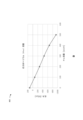
図4A~図4Bは、本明細書に記載されているスパッタリングプロセス(例えば、マグネトロンスパッタリングプロセス)を使用して形成されたAlN層の応力を示す例示的なプロット400の図表である。図4Aに示されるように、AlN層の応力は、Arを含む不活性ガスが120~370標準立方センチメートル/分(sccm)の流量で(例えば、図3に関して本明細書に記載されているスパッタ堆積システムの真空チャンバ310に)供給されるときに、-230~650MPaになるように設定することができる。図4Bに示されるように、AlN層の応力は、Heを含む不活性ガスが0~500sccmの流量で(例えば、図3に関して本明細書に記載されているスパッタ堆積システムの真空チャンバ310に)供給されるときに、-950~175MPaとなるように設定することができる。いくつかの実装形態では、Arを含む不活性ガスも、120~370sccmの流量で(例えば、図3に関して本明細書に記載されているスパッタ堆積システムの真空チャンバ310に)供給される。
4A-4B are diagrams of
上述のように、図4A~図4Bは一例として提示される。他の例は、図4A~図4Bに関して説明したものとは異なる場合がある。 As noted above, FIGS. 4A-4B are presented as an example. Other examples may differ from those described with respect to FIGS. 4A-4B.
図5は、本明細書に記載されているスパッタリングプロセス(例えば、マグネトロンスパッタリングプロセス)を使用して形成されたAlN層のセットの吸光係数(k)及び屈折率(r)の例示的なプロット500である。図5に示されるように、吸光係数は、500~2000nmの波長を有する光に対して0.001未満にすることができる。図5にさらに示されるように、屈折率は、500~2000nmの波長を有する光に対して2.2未満にすることができる。
FIG. 5 is an
上記のように、図5は一例として提示される。他の実施例は、図5に関して説明したものとは異なる場合がある。 As noted above, FIG. 5 is provided as an example. Other embodiments may differ from those described with respect to FIG.
図6は、本明細書に記載されている光学フィルタ(例えば、光学フィルタ200)の透過性能を示す例示的なプロット600の図表である。光学フィルタは、AlN材料を含む層の第1のサブセット(例えば、層の第1のサブセット230)と、Si:H材料を含む層の第2のサブセット(例えば、層の第2のサブセット240)と、を含む層のセット(例えば、層のセット220)を備える。図6に示されるように、光学フィルタは、920~960nmの波長を有する光のうち約85%超(ピークが約92%である)を透過させることができる。これに対し、Ta2O5材料を含む層の第1のサブセットと、Si:H材料を含む層の第2のサブセットと、を有する層のセットを備える代替的な光学フィルタは、920~960nmの波長を有する光のうち約60%超(ピークが約67%である)を透過させることができる。したがって、本明細書に記載されている光学フィルタは、920~960nmのスペクトル域における代替の光学フィルタと比較して、改善された透過性能を有する。
FIG. 6 is a diagram of an
上記のように、図6は一例として提示される。他の例は、図6に関して説明したものとは異なる場合がある。 As noted above, FIG. 6 is presented as an example. Other examples may differ from those described with respect to FIG.
図7A~7Cは、本明細書に記載されている例示的な実装形態の光学特性及び物理的特性の図表700/710/720である。 7A-7C are diagrams 700/710/720 of optical and physical properties of exemplary implementations described herein.
図7Aに示されるように、図表700は、光学フィルタ(例えば、本明細書に記載されている光学フィルタ200)の角度シフト性能を示す。光学干渉フィルタの中心波長における角度シフトは、入射角(図7Aにθとして示される)が0度~30度の場合、中心波長の1.0%未満にすることができる。例えば、光学フィルタが中心波長を940ナノメートル(nm)に設定されている場合、光学フィルタは、最大30度の入射角で、例えば9.4nm未満の角度シフトを有し得る。いくつかの実装形態では、光学フィルタが、最大30度の入射角で、7.0nm未満の角度シフトを有し得る。この場合、光学フィルタは、例えば、3.7、4.0、4.5、5.0、及び/又は5.5以上の有効屈折率を達成することができる。いくつかの実装形態において、光学フィルタは、中心波長で、80%超、85%超、90%超、及び/又は95%超などの透過率閾値を超える透過率(例えば、入射角が0~30度のときの光学フィルタのピーク透過率)を達成することができる。さらに、光学フィルタは、+/-10%未満、+/-5%未満、又は+/-1%未満のリップル(ripple)を達成することができ、リップルとは、入射角が0度~30度の場合の通過帯域にわたる透過率の偏位を表す。
As shown in FIG. 7A, a
図7B及び7Cに示されるように、図表710及び720は、光学フィルタの例示的な積層及び層厚の例を示す。この場合、光学フィルタは、AlN材料(例えば、500~5500nmの波長を有する光に対して1.9~2.2の屈折率を有する)を含む層と、Si:H-He材料(例えば、500~5500nmの波長を有する光に対して3.5~3.9の屈折率を有する)を含む層とを交互に重ねることによって製造される。光学フィルタは、閾値厚さ(例えば、1つ又は2つ以上の層の次に最も厚い層よりも200%超で厚い厚さ、かつ例えば、次に最も厚い層よりも500%未満で厚い厚さ)よりも大きい1つ又は2つの「厚い層」を含む。いくつかの実装形態では、光学フィルタが2つの厚い層を含んでもよく、またこれらの厚い層同士が10%~25%ずれていてもよい。例えば、2つの厚い層のうち小さい方の層の厚さは、2つの厚い層のうち大きい方の層の厚さよりも10%~25%小さくてもよい。 As shown in FIGS. 7B and 7C, diagrams 710 and 720 show examples of exemplary stacks and layer thicknesses for optical filters. In this case, the optical filter includes a layer containing AlN material (eg, having a refractive index of 1.9-2.2 for light having a wavelength of 500-5500 nm) and a Si:H—He material (eg, (having a refractive index of 3.5-3.9 for light with a wavelength of 500-5500 nm). The optical filter has a threshold thickness (e.g., one or more layers greater than 200% greater than the next thickest layer, and e.g., less than 500% greater than the next thickest layer). 1 or 2 "thick layers" that are greater than In some implementations, the optical filter may include two thick layers and the thick layers may be offset by 10% to 25%. For example, the thickness of the smaller of the two thick layers may be 10% to 25% less than the thickness of the larger of the two thick layers.
上述のように、図7A~7Cは、単なる一例として提示される。他の例は、図7A~図7Cに関して説明したものとは異なる場合がある。 As noted above, FIGS. 7A-7C are provided as an example only. Other examples may differ from those described with respect to FIGS. 7A-7C.
図8A~8Cは、本明細書に記載されている例示的な実装形態の光学特性及び物理的特性の図表800/810/820である。 8A-8C are diagrams 800/810/820 of optical and physical properties of exemplary implementations described herein.
図8Aに示されるように、図表800は光学フィルタ(例えば、本明細書に記載されている光学フィルタ200)の角度シフト性能を示す。光学干渉フィルタの中心波長における角度シフトは、入射角(図8Aにθとして示される)が0度~30度の場合、中心波長の1.0%未満にすることができる。例えば、光学フィルタが中心波長を940ナノメートル(nm)に設定されている場合、光学フィルタは、最大30度の入射角で、例えば、9.4nm未満の角度シフトを有することができる。いくつかの実装形態では、光学フィルタが、最大30度の入射角で7.0nm未満の角度シフトを有することができる。この場合、光学フィルタは、例えば、3.7、4.0、4.5、5.0、及び/又は5.5以上の有効屈折率を達成することができる。いくつかの実装形態において、光学フィルタは、中心波長で、80%超、85%超、90%超、及び/又は95%超などの透過率閾値を超える透過率(例えば、入射角が0~30度のときの光学フィルタのピーク透過率)を達成することができる。さらに、光学フィルタは、+/-10%未満、+/-5%未満、又は+/-1%未満のリップルを達成することができ、リップルは、入射角が0~30度の場合の通過帯域にわたる透過率の偏位を表す。
As shown in FIG. 8A, a
図8B及び8Cに示されるように、図表810及び820は、光学フィルタの積層例及び層厚の例を示す。この場合、光学フィルタは、AlN材料(例えば、500~5500nmの波長を有する光に対して1.9~2.2の屈折率を有する)を含む層と、Si:H-He材料(例えば、500~5500nmの波長を有する光に対して3.5~3.9の屈折率を有する)を含む層とを交互に重ねることによって製造される。また光学フィルタは、SiO2材料を含む追加の層(例えば、本明細書に記載されているようなキャップ層)を備えることもできる。 As shown in FIGS. 8B and 8C, charts 810 and 820 show example stacks and layer thicknesses for optical filters. In this case, the optical filter includes a layer containing AlN material (eg, having a refractive index of 1.9-2.2 for light having a wavelength of 500-5500 nm) and a Si:H—He material (eg, (having a refractive index of 3.5-3.9 for light with a wavelength of 500-5500 nm). The optical filter may also comprise additional layers (eg, cap layers as described herein) comprising SiO2 material.
上述のように、図8A~8Cは単なる一例として提示される。他の例は、図8A~8Cに関して説明したものと異なってもよい。 As noted above, FIGS. 8A-8C are provided as an example only. Other examples may differ from those described with respect to Figures 8A-8C.
前述の開示は例示及び説明を与えるものだが、網羅的であること、又は実装形態を開示されている厳密な形態に限定することを意図するものではない。修正及び変形は、上記の開示に照らしてなされてもよく、又は実装形態の実施から得られてもよい。 The foregoing disclosure, while exemplary and explanatory, is not intended to be exhaustive or to limit implementations to the precise forms disclosed. Modifications and variations may be made in light of the above disclosure, or may be acquired from practice of the implementations.
本明細書で使用する場合、用語「コンポーネント」は、ハードウェア、ファームウェア、又はハードウェアとソフトウェアの組合せとして広く解釈されるように意図される。本明細書に記載されているシステム及び/又は方法がハードウェア、ファームウェア、及び/又はハードウェアとソフトウェアの組合せの異なる形態で実装されてもよいことは、明らかであろう。これらのシステム及び/又は方法を実施するために使用される実際の専用制御ハードウェア又はソフトウェアコードは、実装形態を限定するものではない。したがって、システム及び/又は方法の動作及び挙動は、特定のソフトウェアコードを参照することなく本明細書に記載され、本明細書の説明に基づいてシステム及び/又は方法を実装するためにソフトウェア及びハードウェアが使用されてもよいことが理解される。 As used herein, the term "component" is intended to be interpreted broadly as hardware, firmware, or a combination of hardware and software. It will be appreciated that the systems and/or methods described herein may be implemented in different forms in hardware, firmware, and/or a combination of hardware and software. The actual specialized control hardware or software code used to implement these systems and/or methods is not limiting of implementations. Accordingly, the operation and behavior of systems and/or methods are described herein without reference to specific software code, and software and hardware implementations to implement the systems and/or methods based on the description herein. It is understood that ware may be used.
本明細書で使用される場合、閾値を満たすとは、文脈に応じて、閾値よりも大きい、閾値以上、閾値よりも小さい、閾値以下、閾値に等しい、閾値に等しくない等の値を指すことがある。 As used herein, meeting a threshold refers to values such as greater than threshold, greater than or equal to threshold, less than threshold, less than or equal to threshold, equal to threshold, and not equal to threshold, depending on the context. There is
特徴の特定の組合せが特許請求の範囲に記載され、かつ/又は本明細書に開示されているが、これらの組合せは、様々な実装形態の開示を限定することを意図するものではない。実際、これらの特徴の多くは、特許請求の範囲に具体的に記載されていない、及び/又は本明細書に開示されていない方法で組み合わせることができる。以下に列挙される各従属クレームは、1つの請求項のみに直接依存するが、様々な実装形態の開示は、請求項のセットにおける他のすべての請求項と組み合わせられた各従属クレームを含む。本明細書で使用する場合、項目のリスト「のうちの少なくとも1つ」を指す語句は、単一要素を含む、それらの項目の任意の組合せを指す。一例として、「a、b、又はcのうちの少なくとも1つ」は、a、b、c、a-b、a-c、b-c、及びa-b-c、ならびに同じ項目の倍数との任意の組合せを包含することが意図される。 Although specific combinations of features are claimed and/or disclosed herein, these combinations are not intended to limit the disclosure of various implementations. Indeed, many of these features can be combined in ways not specifically recited in the claims and/or disclosed herein. Each dependent claim listed below directly depends on only one claim, but the disclosure of various implementations includes each dependent claim in combination with every other claim in the set of claims. As used herein, a phrase referring to “at least one of” a list of items refers to any combination of those items, including single elements. As an example, "at least one of a, b, or c" includes a, b, c, ab, ac, bc, and abc, and multiples of the same item. is intended to encompass any combination of
本明細書で使用される要素、行為、又は命令は、そうであると明示的に記載されない限り、重要又は必須であると解釈されるべきではない。また、本明細書で使用される場合、冠詞「a」及び「an」は1つ以上の項目を含むことが意図され、本明細書で使用される場合、冠詞「the」は冠詞「the」に関連して参照される1つ以上の項目を含むことが意図され、「1つ以上(the one or more)」と互換的に使用され得る。さらに、本明細書で使用される場合、用語「セット(set)」は、1つ以上の項目(例えば、関連する項目、無関係な項目、又は関連する項目と無関係な項目の組合せ)を含むことが意図され、「1つ以上」と互換的に使用され得る。また、本明細書で使用する場合、用語「有する(have, has, having)」などは、オープンエンドの用語であることが意図される。さらに、「~に基づく(based on)」という語句は、特に明記しない限り、「~に少なくとも部分的に基づく(based, at least in part, on)」ように意図される。また、本明細書で使用される場合、用語「又は(or)」は、連続して使用される場合に包括的であることが意図され、明示的に別段の定め(例えば、「いずれか」又は「一方のみ」と組み合わせて使用される場合)がない限り、「及び/又は(and/or)」と互換的に使用され得る。
No element, act, or instruction used herein should be construed as critical or essential unless explicitly stated as such. Also, as used herein, the articles "a" and "an" are intended to include one or more items and, as used herein, the article "the" refers to the article "the". is intended to include one or more items referenced in connection with, and may be used interchangeably with "the one or more." Further, as used herein, the term "set" includes one or more items (e.g., related items, unrelated items, or a combination of related and unrelated items). is intended and may be used interchangeably with "one or more." Also, as used herein, the terms "have, has, having," etc. are intended to be open-ended terms. Further, the phrase "based on" is intended to be "based, at least in part, on," unless otherwise specified. Also, as used herein, the term "or" when used consecutively is intended to be inclusive and expressly specified otherwise (e.g., "either"). or "and/or" may be used interchangeably unless "and/or" is used in combination with "only one").
Claims (20)
前記基板上に配置される層のセットと、
を備える光学干渉フィルタであって、
前記層のセットは、
層の第1のサブセット、及び
層の第2のサブセット、
を有し、
各前記層の第1のサブセットは窒化アルミニウム(AlN)材料を含み、
各前記層の第1のサブセットの応力は-1000~800メガパスカルであり、
前記層の第1のサブセットは、第1の値を有する第1の屈折率を有し、
各前記層の第2のサブセットは少なくとも1つの他の材料を含み、
前記層の第2のサブセットは、前記第1の値と異なる第2の値を有する第2の屈折率を有し、
前記光学干渉フィルタは、前記第1の値及び前記第2の値のうち最高値の95%以上の有効屈折率を有する、光学干渉フィルタ。 a substrate and a set of layers disposed on said substrate;
An optical interference filter comprising:
The set of layers includes:
a first subset of layers; and a second subset of layers;
has
a first subset of each said layer comprising an aluminum nitride (AlN) material;
the stress of a first subset of each said layer is between -1000 and 800 megapascals;
a first subset of the layers having a first refractive index with a first value;
a second subset of each said layer comprising at least one other material;
a second subset of the layers has a second refractive index having a second value different from the first value;
The optical interference filter has an effective refractive index equal to or greater than 95% of the highest value of the first value and the second value.
シリコン(Si)材料、
水素化シリコン(Si:H)材料、
水素化シリコン-ヘリウム(Si:H-He)材料、
シリコン及び水素材料(SiH)材料、
アモルファスシリコン(a-Si)材料、
窒化シリコン(SiN)材料、
ゲルマニウム(Ge)材料、
水素化ゲルマニウム(Ge:H)材料、
シリコンゲルマニウム(SiGe)材料、
水素化シリコンゲルマニウム(SiGe:H)材料、
炭化ケイ素(SiC)材料、
水素化炭化ケイ素(SiC:H)材料、
二酸化ケイ素(SiO2)材料、
五酸化タンタル(Ta2O5)材料、
五酸化ニオブ(Nb2O5)材料、
酸化ニオブチタン(NbTiOx)材料、
五酸化ニオブタンタル(Nb2-xTaxO5)材料、
二酸化チタン(TiO2)材料、
酸化アルミニウム(Al2O3)材料、
酸化ジルコニウム(ZrO2)材料、
酸化イットリウム(Y2O3)材料、又は
酸化ハフニウム(HfO2)材料、
のうち少なくとも1つを含む、光学干渉フィルタ。 2. The optical interference filter of claim 1, wherein said at least one other material comprises
Silicon (Si) material,
Silicon hydride (Si:H) materials,
hydrogenated silicon-helium (Si:H-He) materials,
silicon and hydrogen materials (SiH) materials,
amorphous silicon (a-Si) material,
silicon nitride (SiN) material,
germanium (Ge) material,
germanium hydride (Ge:H) material,
silicon germanium (SiGe) material,
silicon germanium hydride (SiGe:H) material,
silicon carbide (SiC) material,
hydrogenated silicon carbide (SiC:H) materials,
Silicon dioxide ( SiO2 ) materials,
Tantalum pentoxide ( Ta2O5 ) material,
Niobium pentoxide ( Nb2O5 ) material ,
niobium titanium oxide (NbTiO x ) material,
Niobium pentoxide (Nb 2-x Ta x O 5 ) materials,
titanium dioxide ( TiO2 ) material,
Aluminum oxide ( Al2O3 ) material ,
Zirconium oxide ( ZrO2 ) material,
yttrium oxide ( Y2O3 ) material , or hafnium oxide ( HfO2 ) material,
an optical interference filter comprising at least one of
層の第2のサブセット、
を有する層のセットを備える光学干渉フィルタであって、
各前記層の第1のサブセットは、窒化アルミニウム(AlN)材料を含み、
前記層の第1のサブセットは、第1の値を有する第1の屈折率を有し、
各前記層の第2のサブセットは、水素化シリコン-ヘリウム(Si:H-He)材料を含み、
前記層の第2のサブセットは、前記第1の値よりも大きい第2の値を有する第2の屈折率を有し、
前記光学干渉フィルタは、前記第2の値の95%以上の有効屈折率を有する、光学干渉フィルタ。 a first subset of layers; and a second subset of layers;
An optical interference filter comprising a set of layers having
a first subset of each said layer comprising an aluminum nitride (AlN) material;
a first subset of the layers having a first refractive index with a first value;
a second subset of each said layer comprising a hydrogenated silicon-helium (Si:H-He) material;
a second subset of the layers has a second refractive index having a second value greater than the first value;
An optical interference filter, wherein the optical interference filter has an effective refractive index greater than or equal to 95% of the second value.
前記層の第1のサブセット及び前記層の第2のサブセットのうち他方は圧縮材を含む、光学干渉フィルタ。 9. The optical interference filter of claim 8, wherein one of said first subset of layers and said second subset of layers comprises a tensile material, and said first subset of layers and said second subset of layers An optical interference filter, wherein the other of the two subsets comprises compression material.
前記第1の値は、500~5500ナノメートルの波長を有する光に対して、1.9~2.2であり、
前記第2の値は、500~5500ナノメートルの波長を有する光に対して、3.5~3.9である、光学干渉フィルタ。 9. An optical interference filter according to claim 8,
said first value is between 1.9 and 2.2 for light having a wavelength between 500 and 5500 nanometers;
An optical interference filter, wherein said second value is between 3.5 and 3.9 for light having a wavelength between 500 and 5500 nanometers.
前記追加の層は二酸化ケイ素(SiO2)材料を含む、請求項8に記載の光学干渉フィルタ。 9. The optical interference filter of claim 8, wherein additional layers are disposed above the set of layers,
9. The optical interference filter of claim 8, wherein said additional layer comprises silicon dioxide (SiO2) material.
チャンバへ窒素ガス(N2)を供給するステップと、並びに
前記不活性ガス及び前記N2ガスを供給することに基づいて、アルミニウム(Al)ターゲットをスパッタリングさせて、基板上に窒化アルミニウム(AlN)を含む層の第1のセットを形成するステップと、
を含む方法であって、
前記層の第1のセットを、層の第2のセットと交互になるように前記基板上に形成することにより、層の配列を形成し、
前記層の第2のセットは、水素化シリコン-ヘリウム(Si:H-He)を含み、
前記層の配列は、3.7以上の有効屈折率を有する、方法。 supplying an inert gas to the chamber, the inert gas comprising at least one of argon (Ar) or helium (He);
supplying nitrogen gas ( N2 ) to the chamber, and sputtering an aluminum (Al) target to form aluminum nitride (AlN) on the substrate based on supplying the inert gas and the N2 gas; forming a first set of layers comprising
a method comprising
forming an array of layers by forming the first set of layers on the substrate in an alternating fashion with the second set of layers;
the second set of layers comprises silicon-helium hydride (Si:H-He);
The method of claim 1, wherein the arrangement of layers has an effective refractive index of 3.7 or greater.
前記不活性ガスはHeを含み、
前記層の第1のセットの応力が、-1000~150メガパスカルであり、
前記層の第1のセットの屈折率が、500~5500ナノメートルの波長を有する光に対して、1.9~2.2である、方法。 19. The method of claim 18, wherein
the inert gas contains He;
the stress of the first set of layers is between -1000 and 150 megapascals;
The method, wherein the refractive index of the first set of layers is between 1.9 and 2.2 for light having wavelengths between 500 and 5500 nanometers.
前記方法はさらに、
前記チャンバに水素(H2)ガスを供給するステップと、
前記不活性ガス及び前記H2ガスを供給することに基づいて、前記シリコン(Si)ターゲットをスパッタリングさせて、Si:H-Heを有する前記層の第2のセットを形成するステップと、
を含む、方法。
19. The method of claim 18, wherein the inert gas comprises helium (He),
The method further comprises:
supplying hydrogen (H 2 ) gas to the chamber;
sputtering the silicon (Si) target to form a second set of layers comprising Si:H—He based on supplying the inert gas and the H 2 gas;
A method, including
Applications Claiming Priority (2)
| Application Number | Priority Date | Filing Date | Title |
|---|---|---|---|
| US17/457,123 US20230168418A1 (en) | 2021-12-01 | 2021-12-01 | Optical interference filter |
| US17/457,123 | 2021-12-01 |
Publications (1)
| Publication Number | Publication Date |
|---|---|
| JP2023081852A true JP2023081852A (en) | 2023-06-13 |
Family
ID=84367298
Family Applications (1)
| Application Number | Title | Priority Date | Filing Date |
|---|---|---|---|
| JP2022188210A Pending JP2023081852A (en) | 2021-12-01 | 2022-11-25 | optical interference filter |
Country Status (5)
| Country | Link |
|---|---|
| US (1) | US20230168418A1 (en) |
| EP (1) | EP4191294A1 (en) |
| JP (1) | JP2023081852A (en) |
| KR (1) | KR20230082581A (en) |
| CN (1) | CN116203665A (en) |
Family Cites Families (9)
| Publication number | Priority date | Publication date | Assignee | Title |
|---|---|---|---|---|
| DE3404736A1 (en) * | 1983-04-18 | 1984-10-18 | Balzers Hochvakuum Gmbh, 6200 Wiesbaden | THICK LAYER ARRANGEMENT |
| JP4300245B2 (en) * | 2006-08-25 | 2009-07-22 | キヤノン株式会社 | Optical element equipped with multilayer reflector, surface emitting laser |
| TWI684031B (en) * | 2012-07-16 | 2020-02-01 | 美商唯亞威方案公司 | Optical filter and sensor system |
| US11131018B2 (en) * | 2018-08-14 | 2021-09-28 | Viavi Solutions Inc. | Coating material sputtered in presence of argon-helium based coating |
| US11650361B2 (en) * | 2018-12-27 | 2023-05-16 | Viavi Solutions Inc. | Optical filter |
| WO2020204194A1 (en) * | 2019-04-03 | 2020-10-08 | Agc株式会社 | Optical member |
| KR102055579B1 (en) * | 2019-06-27 | 2019-12-13 | 주식회사 옵트론텍 | Optical filter |
| DE112020006040T5 (en) * | 2019-12-11 | 2022-12-29 | Nippon Electric Glass Co., Ltd. | OPTICAL FILTER AND METHOD OF MAKING THE SAME |
| US20230012033A1 (en) * | 2021-07-07 | 2023-01-12 | Viavi Solutions Inc. | Multi-bandpass optical interference filter |
-
2021
- 2021-12-01 US US17/457,123 patent/US20230168418A1/en active Pending
-
2022
- 2022-11-25 JP JP2022188210A patent/JP2023081852A/en active Pending
- 2022-11-29 CN CN202211514210.3A patent/CN116203665A/en active Pending
- 2022-11-29 KR KR1020220163450A patent/KR20230082581A/en unknown
- 2022-11-30 EP EP22210677.5A patent/EP4191294A1/en active Pending
Also Published As
| Publication number | Publication date |
|---|---|
| US20230168418A1 (en) | 2023-06-01 |
| EP4191294A1 (en) | 2023-06-07 |
| KR20230082581A (en) | 2023-06-08 |
| CN116203665A (en) | 2023-06-02 |
Similar Documents
| Publication | Publication Date | Title |
|---|---|---|
| JP7404367B2 (en) | optical filter | |
| CN108121026B (en) | Silicon germanium based optical filter | |
| US11733442B2 (en) | Optical filter | |
| KR20230104573A (en) | Argon-helium based coating | |
| EP4155786A1 (en) | Optical interference filter | |
| TW202341450A (en) | Optical interference filter | |
| JP2023081852A (en) | optical interference filter | |
| US11867935B2 (en) | Optical interference filter | |
| EP4328637A1 (en) | Optical interference filter | |
| US20230288620A1 (en) | Optical interference filter | |
| EP4336230A1 (en) | Optical interference filter | |
| TWI834789B (en) | Optical filter |