JP2022166330A - Improved charged particle detector - Google Patents
Improved charged particle detector Download PDFInfo
- Publication number
- JP2022166330A JP2022166330A JP2022135958A JP2022135958A JP2022166330A JP 2022166330 A JP2022166330 A JP 2022166330A JP 2022135958 A JP2022135958 A JP 2022135958A JP 2022135958 A JP2022135958 A JP 2022135958A JP 2022166330 A JP2022166330 A JP 2022166330A
- Authority
- JP
- Japan
- Prior art keywords
- section
- dynode
- electron multiplier
- conversion dynode
- relatively
- Prior art date
- Legal status (The legal status is an assumption and is not a legal conclusion. Google has not performed a legal analysis and makes no representation as to the accuracy of the status listed.)
- Granted
Links
Images


Classifications
-
- H—ELECTRICITY
- H01—ELECTRIC ELEMENTS
- H01J—ELECTRIC DISCHARGE TUBES OR DISCHARGE LAMPS
- H01J49/00—Particle spectrometers or separator tubes
- H01J49/02—Details
- H01J49/025—Detectors specially adapted to particle spectrometers
-
- H—ELECTRICITY
- H01—ELECTRIC ELEMENTS
- H01J—ELECTRIC DISCHARGE TUBES OR DISCHARGE LAMPS
- H01J43/00—Secondary-emission tubes; Electron-multiplier tubes
- H01J43/04—Electron multipliers
- H01J43/30—Circuit arrangements not adapted to a particular application of the tube and not otherwise provided for
-
- H—ELECTRICITY
- H01—ELECTRIC ELEMENTS
- H01J—ELECTRIC DISCHARGE TUBES OR DISCHARGE LAMPS
- H01J49/00—Particle spectrometers or separator tubes
- H01J49/0027—Methods for using particle spectrometers
- H01J49/0031—Step by step routines describing the use of the apparatus
-
- H—ELECTRICITY
- H01—ELECTRIC ELEMENTS
- H01J—ELECTRIC DISCHARGE TUBES OR DISCHARGE LAMPS
- H01J49/00—Particle spectrometers or separator tubes
- H01J49/26—Mass spectrometers or separator tubes
- H01J49/34—Dynamic spectrometers
- H01J49/42—Stability-of-path spectrometers, e.g. monopole, quadrupole, multipole, farvitrons
- H01J49/4205—Device types
- H01J49/4255—Device types with particular constructional features
Landscapes
- Chemical & Material Sciences (AREA)
- Analytical Chemistry (AREA)
- Electron Tubes For Measurement (AREA)
- Other Investigation Or Analysis Of Materials By Electrical Means (AREA)
Abstract
Description
本発明は、概して、科学分析機器の構成要素、および分析機器の完備品に関する。より具体的には、排他的ではないが、本発明は、質量分析用途でイオンを検出するために有用な装置および方法に関する。 The present invention relates generally to components of scientific analytical instruments and to complete analytical instruments. More particularly, but not exclusively, the present invention relates to apparatus and methods useful for detecting ions in mass spectrometry applications.
多くの科学用途では、電子信号を増幅する必要がある。例えば、質量分析計では、分析対象物がイオン化されて、様々な荷電粒子(イオン)が形成される。結果物であるイオンは、次いで、通常、加速および電界または磁界への露出によって、質量対電荷比に従って分離される。分離された信号イオンは、イオン検出器表面に衝突して、1つ以上の二次電子を生成する。結果は、質量対電荷比の関数として、検出されたイオンの相対存在量のスペクトルとして表示される。 Many scientific applications require amplification of electronic signals. For example, in a mass spectrometer, an analyte is ionized to form various charged particles (ions). The resulting ions are then separated according to their mass-to-charge ratio, usually by acceleration and exposure to an electric or magnetic field. The separated signal ions strike an ion detector surface to produce one or more secondary electrons. Results are displayed as a spectrum of relative abundance of detected ions as a function of mass-to-charge ratio.
他の用途では、検出される粒子は、イオンでなくてもよく、中性原子、中性分子、電子、または光子であってもよい。いずれにせよ、粒子が衝突する検出器表面が依然として提供される。 In other applications, the particles to be detected may not be ions, but may be neutral atoms, neutral molecules, electrons, or photons. In any event, a detector surface is still provided on which the particles impinge.
検出器の衝突表面に対する入力粒子の衝突から結果として生じる二次電子は、通常、電子増倍器によって増幅される。電子増倍器は、概して、二次電子放出によって動作し、それによって、増倍器衝突表面に対する単一または複数の粒子の衝突が、衝突表面の原子に関連付けられた単一または(好ましくは)複数の電子を放出させる。 Secondary electrons resulting from the impact of the input particles against the impact surface of the detector are typically amplified by an electron multiplier. Electron multipliers generally operate by secondary electron emission whereby the impact of single or multiple particles on the multiplier impact surface produces single or (preferably) particles associated with the atoms of the impact surface. Emit multiple electrons.
いくつかの用途では、他の種の中でも単一イオンの検出を可能にするために、非常に高い感度レベルを有する粒子検出器が必要とされる。例えば、誘導結合プラズマ質量分析(ICP-MS)は、分析中の原子をイオンに変換する(ICP源で)。そのように形成されたイオンは、次いで、分離され、質量分析計によって検出される。ICP-MSは、通常、出力の非常に広いダイナミックレンジを処理するために、専用の電子増倍器の使用を必要とする。先行技術では、単一イオンの衝突から生じる非常に低い信号を依然として検出することができる一方で、複数のイオンから結果として生じる非常に高いレベルの信号に対処し得る様々な増倍器が公知である。 Some applications require particle detectors with very high sensitivity levels to allow detection of single ions among other species. For example, inductively coupled plasma-mass spectrometry (ICP-MS) converts the atoms under analysis into ions (at the ICP source). The ions so formed are then separated and detected by a mass spectrometer. ICP-MS usually requires the use of dedicated electron multipliers to handle the very wide dynamic range of the output. In the prior art, various multipliers are known that are capable of coping with the very high level of signals resulting from multiple ions while still being able to detect very low signals resulting from single ion collisions. be.
感度レベルに関係なく、ダイナミックレンジのさらなる改善が、それでもなお当技術分野で望まれている。出願人の知る限り、1990年代に導入されて以来、これらの器具のダイナミックレンジに実質的な改善はなかった。 Further improvements in dynamic range, regardless of sensitivity level, are still desired in the art. To the applicant's knowledge, there has been no substantial improvement in the dynamic range of these instruments since their introduction in the 1990's.
検出効率、応答の線形性、ゲインの安定性、差動ドリフトおよび耐用年数の領域の改善もまた、概して、当技術分野で望まれている。 Improvements in the areas of detection efficiency, response linearity, gain stability, differential drift and service life are also generally desired in the art.
さらに、当技術分野では、質量分析計器具の構造を単純化し、任意の変換表面および/または電子放出表面の保守および交換を容易にすることも望まれている。 Additionally, there is a desire in the art to simplify the construction of mass spectrometer instrumentation and facilitate maintenance and replacement of any conversion and/or electron emitting surfaces.
文書、作用、材料、デバイス、物品などの議論は、本発明の文脈を提供する目的のためだけに本明細書に含まれる。これらの事項のいずれかまたは全てが、先行技術の基礎の一部を形成したこと、または本出願の各請求項の優先日以前に存在したものとして、本発明に関連する分野において共通の一般知識であったことは、示唆または表明されていない。 Discussion of documents, acts, materials, devices, articles, etc. is included herein only for the purpose of providing a context for the invention. Any or all of these matters form part of the prior art basis or existed prior to the priority date of each claim of the present application, common general knowledge in the fields relevant to the present invention. It is not implied or stated that
第1の態様では、必ずしも本発明の広範な態様ではないが、荷電粒子を検出するための装置が提供され、装置は、粒子による衝突の際に1つ以上の二次電子またはイオンを放出するように構成された変換ダイノードと、変換ダイノードによって放出された1つ以上の二次電子またはイオンから増幅された電子信号出力を形成するように構成された電子増倍器と、を備える。 In a first aspect, although not necessarily a broader aspect of the invention, there is provided an apparatus for detecting charged particles, the apparatus emitting one or more secondary electrons or ions upon collision with the particles. and an electron multiplier configured to form an amplified electronic signal output from one or more secondary electrons or ions emitted by the conversion dynode.
第1の態様の一実施形態では、電子増倍器が、相対的低感度区分および相対的高感度区分を有する。 In one embodiment of the first aspect, the electron multiplier has a relatively low sensitivity section and a relatively high sensitivity section.
第1の態様の一実施形態では、変換ダイノードが、電子増倍器とは別々に電力供給される。 In one embodiment of the first aspect, the conversion dynode is powered separately from the electron multiplier.
第1の態様の一実施形態では、変換ダイノードが、高エネルギー変換ダイノードである。 In one embodiment of the first aspect, the conversion dynode is a high energy conversion dynode.
第1の態様の一実施形態では、変換ダイノードが、電子増倍器内またはその周りに物理的に組み込まれている。 In one embodiment of the first aspect, the conversion dynode is physically embedded within or around the electron multiplier.
第2の態様では、本発明は、荷電粒子を検出するための装置を提供し、装置は、粒子による衝突の際に1つ以上の二次電子またはイオンを放出するように構成された変換ダイノードと、変換ダイノードによって放出された1つ以上の二次電子またはイオンから増幅された電子信号出力を形成するように構成された電子増倍器と、を備え、変換ダイノードが、電子増倍器内またはその周りに物理的に組み込まれている。 In a second aspect, the invention provides an apparatus for detecting charged particles, the apparatus being a conversion dynode configured to emit one or more secondary electrons or ions upon impact with the particles. and an electron multiplier configured to form an amplified electronic signal output from one or more secondary electrons or ions emitted by the conversion dynode, wherein the conversion dynode is within the electron multiplier. or physically built around it.
第2の態様の一実施形態では、変換ダイノードが、電子増倍器とは別々に電力供給されていて、および/または電子増倍器のダイノードに電気的に連結されていない。 In one embodiment of the second aspect, the conversion dynode is powered separately from the electron multiplier and/or is not electrically coupled to the dynode of the electron multiplier.
第2の態様の一実施形態では、電子増倍器が、相対的低感度区分および相対的高感度区分を有する。 In one embodiment of the second aspect, the electron multiplier has a relatively low sensitivity section and a relatively high sensitivity section.
第2の態様の一実施形態では、変換ダイノードが、電子増倍器とは別々に電力供給されていて、および/または電子増倍器のダイノードに電気的に連結されていない。 In one embodiment of the second aspect, the conversion dynode is powered separately from the electron multiplier and/or is not electrically coupled to the dynode of the electron multiplier.
第2の態様の一実施形態では、変換ダイノードは、高エネルギー変換ダイノードである。 In one embodiment of the second aspect, the conversion dynode is a high energy conversion dynode.
第3の態様では、本発明は、荷電粒子を検出するための装置を提供し、装置は、粒子による衝突の際に1つ以上の二次電子またはイオンを放出するように構成された変換ダイノードと、変換ダイノードによって放出された1つ以上の二次電子またはイオンから増幅された電子信号出力を形成するように構成された電子増倍器と、を備え、変換ダイノードが、電子増倍器とは別々に電力供給されていて、および/または電子増倍器のダイノードに電気的に連結されていない。 In a third aspect, the present invention provides an apparatus for detecting charged particles, the apparatus configured to emit one or more secondary electrons or ions upon collision with the particles. and an electron multiplier configured to form an amplified electronic signal output from one or more secondary electrons or ions emitted by the conversion dynode, the conversion dynode comprising the electron multiplier and are separately powered and/or not electrically coupled to the dynodes of the electron multiplier.
第3の態様の一実施形態では、変換ダイノードが、高エネルギー変換ダイノードである。 In one embodiment of the third aspect, the conversion dynode is a high energy conversion dynode.
第3の態様の一実施形態では、変換ダイノードが、電子増倍器内またはその周りに物理的に組み込まれている。 In one embodiment of the third aspect, the conversion dynode is physically embedded within or around the electron multiplier.
第3の態様の一実施形態では、電子増倍器が、相対的低感度区分および相対的高感度区分を有する。 In one embodiment of the third aspect, the electron multiplier has a relatively low sensitivity section and a relatively high sensitivity section.
第1の態様または第2の態様または第3の態様の一実施形態では、相対的高感度区分の電子信号出力が、相対的低感度区分の電子信号出力と比較して、相対的に高ゲインの電子信号出力である。 In one embodiment of the first aspect or the second aspect or the third aspect, the electronic signal output of the relatively high sensitivity section has a relatively high gain compared to the electronic signal output of the relatively low sensitivity section. is the electronic signal output of
第1の態様または第2の態様または第3の態様の一実施形態では、相対的低感度区分が、アナログ区分であり、相対的高感度区分が、様々なパルス高を出力するように構成されたデジタル区分である。 In one embodiment of the first or second or third aspect, the relatively insensitive section is an analog section and the relatively sensitive section is configured to output different pulse heights. digital segmentation.
第1の態様または第2の態様または第3の態様の一実施形態では、デジタル区分出力が、電子計数回路の入力として使用可能であるように構成される。 In one embodiment of the first or second or third aspect, the digital segmented output is configured to be usable as an input of an electronic counting circuit.
第1の態様または第2の態様または第3の態様の一実施形態では、相対的高感度区分および相対的低感度区分が、1つ以上の別個のダイノードを各々備え、電子増倍器は、相対的低感度区分が、相対的に低ゲインの電子信号出力を提供し、相対的高感度区分が、相対的に高ゲインの電子信号出力を提供するように、構成されている。 In one embodiment of the first or second or third aspect, the relatively sensitive section and the relatively insensitive section each comprise one or more separate dynodes, the electron multiplier comprising: The relatively low sensitivity section is configured to provide a relatively low gain electronic signal output and the relatively high sensitivity section is configured to provide a relatively high gain electronic signal output.
第1の態様または第2の態様または第3の態様の一実施形態では、相対的高感度区分および/または相対的低感度区分(複数可)が、少なくとも約5、10、15、20、25、30、35、40、45、50、75または100μAの出力電流で動作するように構成されている。 In one embodiment of the first or second or third aspect, the relatively sensitive segment(s) and/or the relatively insensitive segment(s) are at least about 5, 10, 15, 20, 25 , 30, 35, 40, 45, 50, 75 or 100 μA of output current.
第1の態様または第2の態様または第3の態様の一実施形態では、変換ダイノードが、約+1、+2、+3、+4、+5、+6、+7、+8、+9、+10kV、+15kVもしくは+20kVを超えるか、または約-1、-2、-3、-4、-5、-6、-7、-8、-9、-10、-15もしくは-20kV未満の印加電圧を有する。 In one embodiment of the first or second or third aspect, the conversion dynode is greater than about +1, +2, +3, +4, +5, +6, +7, +8, +9, +10 kV, +15 kV or +20 kV or having an applied voltage less than about -1, -2, -3, -4, -5, -6, -7, -8, -9, -10, -15 or -20 kV.
第1の態様または第2の態様または第3の態様の一実施形態では、変換ダイノードに印加される電圧が、電子増倍器の相対的低感度区分に印加される電圧から分離される。 In one embodiment of the first or second or third aspect, the voltage applied to the conversion dynode is isolated from the voltage applied to the relatively insensitive section of the electron multiplier.
第1の態様または第2の態様または第3の態様の一実施形態では、相対的低感度区分が、少なくとも約6、7、8、9、10、11、12、13、14、15または16個の別個のダイノードを含む。 In one embodiment of the first or second or third aspect, the relative insensitivity segment is at least about 6, 7, 8, 9, 10, 11, 12, 13, 14, 15 or 16 contains separate dynodes.
第1の態様または第2の態様または第3の態様の一実施形態では、相対的高感度区分が、少なくとも約10、11、12、13、14、15、16、17、または18個の別個のダイノードを含む。 In one embodiment of the first or second or third aspect, the relatively sensitive bins are at least about 10, 11, 12, 13, 14, 15, 16, 17, or 18 distinct dynodes.
第1の態様または第2の態様または第3の態様の一実施形態では、変換ダイノードが、電子増倍器の構造と統合されているか、電子増倍器のすぐ隣にあるか、または電子増倍器構造内にある。 In one embodiment of the first or second or third aspect, the conversion dynode is integrated with the structure of the electron multiplier, is immediately adjacent to the electron multiplier, or is Within the doublet structure.
第1の態様または第2の態様または第3の態様の一実施形態では、変換ダイノードに印加される電圧バイアスが、同一装置であるが、変換ダイノードがそれに対して遠位に配設されている場合に印加される電圧バイアスよりも低く、より低い電圧は、変換ダイノードを電子増倍器に近接させることと通常関連付けられるいかなる有害作用も減少または除去されるような電圧である。 In one embodiment of the first or second or third aspect, the voltage bias applied to the conversion dynode is the same device, but the conversion dynode is disposed distal thereto. The lower voltage, which is lower than the voltage bias applied in the case, is such that any detrimental effects normally associated with the proximity of the conversion dynode to the electron multiplier is reduced or eliminated.
第1の態様または第2の態様または第3の態様の一実施形態では、変換ダイノードに印加される電圧バイアスは、約5、4、3、2または1kV未満である。 In one embodiment of the first or second or third aspect, the voltage bias applied to the conversion dynode is less than about 5, 4, 3, 2 or 1 kV.
第4の態様では、本発明は、第1の態様の任意の実施形態の装置を備える質量分析器具を提供する。 In a fourth aspect, the invention provides a mass spectrometry instrument comprising the device of any embodiment of the first aspect.
第4の態様の一実施形態では、質量分析器具が、約1010分の1、1011分の1、1012分の1、1013分の1、1014分の1、または1015分の1未満の濃度で存在する標的粒子を検出するように構成されている。 In one embodiment of the fourth aspect, the mass spectrometry instrument is about 10 10 times, 10 11 times, 10 12 times, 10 13 times, 10 14 times, or 10 15 minutes is configured to detect target particles present at a concentration of less than 1 of .
第4の態様の一実施形態では、質量分析器具が、誘導結合プラズマ質量分析を実施するように構成されている。 In one embodiment of the fourth aspect, the mass spectrometry instrument is configured to perform inductively coupled plasma mass spectrometry.
第5の態様では、本発明は、試料の質量分析を実施する方法を提供し、方法は、第1の態様の任意の実施形態の質量分析器具内に分析用の試料を導入するステップと、1つ以上の電子信号出力(複数可)を提供するように器具を動作させるステップと、を含む。 In a fifth aspect, the invention provides a method of performing mass spectrometric analysis of a sample, the method comprising introducing a sample for analysis into the mass spectrometry instrument of any embodiment of the first aspect; operating the instrument to provide one or more electronic signal output(s).
第5の態様の一実施形態では、質量分析が、約1010分の1、1011分の1、1012分の1、1013分の1、1014分の1、または1015分の1未満の濃度で存在する標的粒子を検出することができる。 In one embodiment of the fifth aspect, the mass spectrometric analysis is about 10 10 times, 10 11 times, 10 12 times, 10 13 times, 10 14 times, or 10 15 times Target particles present at a concentration of less than 1 can be detected.
第5の態様の一実施形態では、質量分析が、誘導結合プラズマ質量分析である。 In one embodiment of the fifth aspect, the mass spectrometry is inductively coupled plasma mass spectrometry.
本説明の検討後、本発明が様々な代替的実施形態および代替的用途にどのように実装されるかが、当業者に明らかとなるであろう。しかしながら、本発明の様々な実施形態が本明細書で説明されることになるが、これらの実施形態は、限定ではなく、単に例として提示されることが理解される。したがって、様々な代替的実施形態の本説明は、本発明の範囲または幅を限定するように解釈されるべきではない。さらに、利点または他の態様の記述は、特定の例示的な実施形態に適用され、必ずしも特許請求の範囲に包含される全ての実施形態に適用されるわけではない。 After reviewing this description, it will become apparent to one skilled in the art how to implement the invention in various alternative embodiments and alternative applications. However, while various embodiments of the present invention will now be described, it is understood that these embodiments are presented by way of example only, and not limitation. Therefore, this description of various alternative embodiments should not be construed to limit the scope or breadth of the invention. Moreover, descriptions of advantages or other aspects apply to particular exemplary embodiments and not necessarily to all embodiments encompassed by the claims.
本明細書の説明および特許請求の範囲全体を通して、「備える(comprise)」という単語、ならびに「備えている(comprising)」および「備える(comprises)」などの単語の変形は、他の付加物、構成要素、整数またはステップを除外することを意図するものではない。 Throughout the description and claims of this specification, the word "comprise" and variations of the word such as "comprising" and "comprises" include other additions, It is not intended to exclude components, integers or steps.
本明細書全体を通して「一実施形態」または「ある実施形態」に対する参照は、その実施形態に関連して説明された特定の特徴、構造または特性が本発明の少なくとも1つの実施形態に含まれることを意味する。したがって、本明細書全体の様々な箇所での「一実施形態では」または「ある実施形態では」という語句の出現は、必ずしも全てが同じ実施形態を参照しているわけではないが、そうであってもよい。 References to "one embodiment" or "an embodiment" throughout this specification indicate that the particular feature, structure or characteristic described in connection with that embodiment is included in at least one embodiment of the invention. means Thus, the appearances of the phrases "in one embodiment" or "in an embodiment" in various places throughout this specification, although they are not necessarily all referring to the same embodiment. may
本明細書に説明される本発明の全ての実施形態が、本明細書に開示される利点の全てを有するわけではないことが理解されるであろう。いくつかの実施形態は、単一の利点を有し得るが、他の実施形態は、全く利点を有しておらず、単に先行技術の有用な代替物である場合がある。 It will be appreciated that not all embodiments of the invention described herein will have all of the advantages disclosed herein. Some embodiments may have a single advantage, while other embodiments may have no advantage at all and simply be a useful alternative to the prior art.
本発明は、少なくとも部分的に出願人の発見に基づいており、この発見は、高感度および低感度区分を有する電子増倍器、または別々に電源供給される変換ダイノード(およびいくつかの実施形態では高エネルギー変換ダイノード)との電子増倍器の組み合わせ、または電子増倍器内もしくはその周りに物理的に組み込まれている変換ダイノードの組み合わせが、先行技術の検出器装置に対して特定の改善を有する検出器装置を提供するというものである。 The present invention is based, at least in part, on Applicants' discovery that an electron multiplier having high and low sensitivity sections, or separately powered conversion dynodes (and in some embodiments, The combination of an electron multiplier with a high energy conversion dynode, or a conversion dynode physically incorporated within or around the electron multiplier, provides certain improvements over prior art detector devices. The object is to provide a detector device having
本明細書で使用される際、「変換ダイノード」という用語は、荷電または非荷電原子、荷電または非荷電分子、中性子、陽子、電子、もしくは光子などの荷電または非荷電亜原子粒子などの、粒子の衝突時に二次電子(またはイオン)を放出することができる任意の仕組みを含むことを意図する。本発明によると、変換ダイノードは、増幅専用のダイノードと比較して相対的に高電位を有するように動作され得る。 As used herein, the term "conversion dynode" refers to particles such as charged or uncharged atoms, charged or uncharged molecules, charged or uncharged subatomic particles such as neutrons, protons, electrons, or photons. It is intended to include any mechanism capable of ejecting secondary electrons (or ions) upon collision of . In accordance with the present invention, conversion dynodes can be operated to have a relatively high potential compared to dynodes dedicated to amplification.
いくつかの実施形態では、ダイノードは「高エネルギー変換ダイノード」である。電位は、必要に応じて、接地または装置の別の構成要素に対して測定され得る。高エネルギー変換ダイノードの定義には、ある程度の相対性が存在し得るが、多くの場合、高エネルギー変換ダイノードおよび電子増倍器の低ゲイン区分の第1のダイノードは、一般的に接地され、高エネルギー変換ダイノードは、電子増倍器の低ゲイン区分の第1のダイノードよりもゼロからさらに離れた電圧でバイアスされている。 In some embodiments, the dynodes are "high energy conversion dynodes." The potential can be measured with respect to ground or another component of the device as desired. Although there may be some relativity in the definition of high energy conversion dynodes, in many cases the first dynode in the low gain section of the high energy conversion dynode and the electron multiplier is commonly grounded and the high The energy conversion dynode is biased at a voltage farther from zero than the first dynode in the low gain section of the electron multiplier.
当業者によって理解されるように、イオンから電子(およびイオンからイオン)への変換効率は、概して、イオンが変換ダイノードの表面に衝突する速度とともに向上する。したがって、変換ダイノードは、通常、実行可能な限り変換効率を最適化するために、入射イオンの速度を上げるように設計される。 As will be appreciated by those skilled in the art, ion-to-electron (and ion-to-ion) conversion efficiency generally increases with the velocity with which the ions collide with the surface of the conversion dynode. Therefore, conversion dynodes are typically designed to increase the velocity of incident ions in order to optimize conversion efficiency wherever possible.
検出器装置における別々に電源供給される別個の変換ダイノードの組み込みは、そのダイノードが、別々に、かつ電子増倍器のダイノード(特に、低ゲイン区分の第1のダイノード)と比較して、より高電圧にバイアスされることを可能にする。本配置の利点は、電子増倍器区分のバイアス電圧を、電子増幅が発生するために必要な電圧よりも高くする必要性を回避することである。ICP-MSに使用される先行技術の検出器では、電子増倍器の初期電圧は、イオンから電子への適切な変換効率を確保するために、約-1600Vまで上げられる。しかしながら、本発明では、変換ダイノードの電圧バイアスは、(所望される変換効率を確保するために)上げられるが、電子増倍器(特に、低ゲイン区分)は、より低電圧でバイアスされ得る。その結果、(より低電圧で動作されている)低ゲイン電子増倍器区分には、より大きな電圧「ヘッドルーム」が提供され、その結果、より長い耐用年数を提供する。 Incorporation of a separate separately powered conversion dynode in the detector apparatus allows the dynode to be separately and more efficient compared to the electron multiplier dynode (particularly the first dynode in the low gain section). Allow it to be biased to a high voltage. An advantage of this arrangement is that it avoids the need to make the bias voltage of the electron multiplier section higher than the voltage required for electron multiplication to occur. In prior art detectors used for ICP-MS, the initial voltage of the electron multiplier is raised to about -1600 V to ensure adequate ion-to-electron conversion efficiency. However, in the present invention, the voltage bias of the conversion dynode is raised (to ensure the desired conversion efficiency) while the electron multiplier (especially the low gain section) can be biased at a lower voltage. As a result, the low gain electron multiplier section (operating at lower voltages) is provided with more voltage "headroom", thus providing a longer useful life.
検出器の耐用年数を延ばすことは、ゲイン変化の速度を遅くする、および/または経時的な差動ドリフトの速度を遅くする、追加の利点を提供し得る。 Extending the useful life of the detector may provide the additional benefit of slowing the rate of gain change and/or slowing the rate of differential drift over time.
高エネルギー変換ダイノードは、通常、装置の電子増倍器区分の電源とは実質的に分離された専用の電源を有する。別々の電源の使用は、高エネルギー変換ダイノードに印加される電圧および/または電流のより良好な独立制御を可能にし得る。別個の電源の使用はまた、電子増倍器区分に印加される電圧および/または電流のより良好な制御を可能にし得る。 High energy conversion dynodes typically have a dedicated power supply that is substantially separate from the power supply of the electron multiplier section of the device. The use of separate power supplies may allow better independent control of the voltage and/or current applied to the high energy conversion dynodes. The use of separate power supplies may also allow better control of the voltage and/or current applied to the electron multiplier section.
装置と関連して使用される電源は、固定電圧タイプであってもよく、または調整可能電圧タイプであってもよい。任意の電源が高エネルギー変換ダイノード、または電子増倍器区分のダイノードチェーン内の任意のダイノードに関連して接続される位置は、装置の線形性またはゲインの要件、または実際には任意の他の要件に従って選択され得る。いくつかの実施形態では、電源は、単一のダイノードのみに、またはダイノードのグループに電圧を印加するように構成され得る。 The power supply used in connection with the device may be of the fixed voltage type or of the adjustable voltage type. The position at which any power supply is connected in relation to the high energy conversion dynode, or any dynode in the dynode chain of the electron multiplier section, depends on the linearity or gain requirements of the device, or indeed any other It can be selected according to requirements. In some embodiments, the power supply may be configured to apply voltage to only a single dynode or to groups of dynodes.
当業者には理解されるように、分圧器チェーンが、電源から一式のダイノードに電圧を分配するために使用され得る。分圧器チェーンは、ダイノード間に配設された一連の抵抗器を含み得る。分圧器チェーンは、抵抗素子のみからなる純粋に受動的なものであってもよく、またはダイオードもしくはトランジスタなどの電圧調整でアクティブな構成要素を含有してもよい。最終ダイノードが関与する場合、抵抗器は、通常、最終ダイノードと接地または基準電圧との間に配設される。代替として、ツェナーダイオードがこの位置で使用されてもよい。 As will be appreciated by those skilled in the art, a voltage divider chain can be used to distribute the voltage from the power supply to a set of dynodes. A voltage divider chain may include a series of resistors disposed between dynodes. The voltage divider chain may be purely passive, consisting only of resistive elements, or may contain components active in voltage regulation, such as diodes or transistors. When a final dynode is involved, the resistor is typically placed between the final dynode and ground or a reference voltage. Alternatively, a Zener diode may be used at this location.
質量分析計の観点から、質量分離器を通過したイオンは、高電圧が印加される変換ダイノード上で加速される。入射イオンによって変換ダイノードから放出された電子(またはイオン)は、次いで、電子増倍器の第1のダイノードに入り、そこで二次電子が二次放出表面から放出される。 From a mass spectrometer point of view, ions passing through a mass separator are accelerated on a conversion dynode to which a high voltage is applied. Electrons (or ions) ejected from the conversion dynode by incident ions then enter the first dynode of the electron multiplier where secondary electrons are emitted from the secondary emitting surface.
当業者は、この文脈における放出表面の材料、物理的および機能的構成に完全に精通しており、例示的なタイプは、ダイノードによって提供されるものである。 Those skilled in the art are thoroughly familiar with the materials, physical and functional configurations of emitting surfaces in this context, an exemplary type being that provided by a dynode.
電子増倍器では従来どおり、入力粒子を受け取り、かつ入力粒子の衝突に応答して1つまたは複数の電子を放出するように構成されている(一連のダイノードの第1のダイノードの)第1の電子放出表面が提供される。複数の電子が放出される場合(通常そうである)、入力信号の増幅が結果として生じる。これも従来どおり、一連の第2および後続の電子放出表面が提供される。これらの放出表面の機能は、第1の放出表面から放出される電子(複数可)を増幅することである。理解されるように、増幅は、通常、一連の放出表面の各後続の放出表面で起こる。通常、最後の放出表面によって放出された二次電子は、アノード表面上に配向され、アノードで形成された電流が、信号増幅器に供給され、続いて、出力デバイスに供給される。 Conventionally in electron multipliers, a first dynode (of a first dynode of a series of dynodes) is configured to receive input particles and emit one or more electrons in response to the impact of the input particles. is provided. If multiple electrons are emitted (which is usually the case), amplification of the input signal results. A series of second and subsequent electron emitting surfaces are provided, also conventionally. The function of these emitting surfaces is to amplify the electron(s) emitted from the first emitting surface. As will be appreciated, amplification typically occurs at each subsequent emitting surface in a series of emitting surfaces. Secondary electrons typically emitted by the last emitting surface are directed onto the anode surface and the current formed at the anode is fed to a signal amplifier and subsequently to an output device.
本発明では、電子増倍器は、相対的に高濃度で存在するイオンを検出するように構成されている低感度区分と、相対的に低濃度で存在するイオンを検出するように構成されている高感度区分とを有し得る。 In the present invention, the electron multiplier has a low sensitivity section configured to detect ions present in relatively high concentrations and a low sensitivity section configured to detect ions present in relatively low concentrations. and a high sensitivity segment.
感度差は、例えば、高感度区分の信号出力が増幅されるが、低感度区分の信号出力が増幅されない、信号増幅器の使用を含む、当業者が適切と考える任意の手段によって提供され得る。代替的に、増倍器が別個のダイノードからなる場合、ダイノードの二次電子放出率のレベルは、低感度区分と比較して高感度区分でより高くなり得る。例えば、高感度区分のダイノードは、低感度区分のダイノードと比較して、より高い放出率であるか、または大きい衝突面積を有する材料から製造され得る。 The sensitivity differential may be provided by any means deemed appropriate by those skilled in the art, including, for example, using a signal amplifier in which the signal output of the high sensitivity section is amplified but the signal output of the low sensitivity section is not. Alternatively, if the multiplier consists of separate dynodes, the level of secondary electron emission rate of the dynodes may be higher in the high sensitivity section compared to the low sensitivity section. For example, dynodes in the high sensitivity section may be made of materials with higher emissivity or larger impingement areas compared to dynodes in the low sensitivity section.
しかしながら、より典型的には、電子増倍器区分の感度差は、高感度区分および低感度区分のゲインの乗算から結果として生じる。高感度区分のより高いゲインは、前の低感度区分のゲインによって乗算されるため、達成される。 More typically, however, the sensitivity difference of the electron multiplier section results from the multiplication of the gains of the high and low sensitivity sections. The higher gain of the high sensitivity section is achieved because it is multiplied by the gain of the previous low sensitivity section.
装置の電子増倍器では、低感度区分は、アナログ区分(低ゲイン区分と見なされ得る)であり得、高感度区分は、パルス計数することができるデジタル区分(高ゲイン区分と見なされ得る)であり得る。デジタル区分からの実効ゲインは、ほぼアナログ区分およびデジタル区分のゲインの積である。したがって、分離して、2つの区分は、同じゲインを有し得るが、デジタル区分は、そのゲインが前のアナログ区分のゲインによって乗算されるため、より高い出力ゲインを有することが理解されるであろう。言い換えると、デジタル区分は、それによって提供される信号が、2つの(アナログおよびデジタル)区分のゲインの積であることにより、アナログ区分によって提供された信号よりも高いゲインであるため、高ゲイン区分と称され得る。デジタル区分によって提供されるゲイン信号は、総ゲインであり、つまり2つの(アナログおよびデジタル)区分のゲインの積である。 In the device's electron multiplier, the low sensitivity section may be an analog section (which may be considered a low gain section) and the high sensitivity section may be a pulse counting digital section (which may be considered a high gain section). can be The effective gain from the digital section is approximately the product of the gains of the analog and digital sections. Thus, in isolation, the two sections may have the same gain, but it should be understood that the digital section has a higher output gain because its gain is multiplied by the gain of the previous analog section. be. In other words, the digital section is a high-gain section because the signal provided by it is of higher gain than the signal provided by the analog section by virtue of being the product of the gains of the two (analog and digital) sections. can be called The gain signal provided by the digital section is the total gain, ie the product of the gains of the two (analog and digital) sections.
いずれにせよ、高感度(デジタル)区分は、少ない数で発生するイオンを検出するように適合される。デジタル区分の出力は、単一イオンから結果として生じるパルスを含み、全てがパルス計数検出電子機器によって検出されるために十分なゲインが提供されている。電子タイマまたはカウンタが、通常、出力パルスを処理するために用いられる。一例として、所定の時間窓と関連付けられたカウンタは、信号がその時間窓内で生成される度に増分され得る。 In any case, the high sensitivity (digital) section is adapted to detect ions occurring in low numbers. The output of the digital section contains the resulting pulse from a single ion, all provided with sufficient gain to be detected by the pulse counting detection electronics. Electronic timers or counters are commonly used to process the output pulses. As an example, a counter associated with a given time window may be incremented each time a signal is generated within that time window.
動作中、パルス計数区分は、非常に高いイオンフラックスが飽和を引き起こすと考えると、限定された範囲を有し、この場合、増倍器のアナログ区分は、有用な出力信号を提供する。本装置では、2つの区分は、中間の「分割」ダイノード、接地ダイノード、および保護(ゲート)ダイノードを有する、直列の2つのダイノードセット配置によって同時に動作可能であり得る。アナログ区分の出力信号は、「分割」ダイノードを介してアナログコレクタ上に抽出される。分割ダイノードの孔を通過する信号の部分がアナログ出力である。孔を通過しない信号の部分は、さらなるゲイン増幅のために電子増倍器のデジタル(パルス)区分に送られる。 In operation, the pulse counting section has a limited range given that very high ion fluxes cause saturation, in which case the analog section of the multiplier provides a useful output signal. In this arrangement, the two sections may be operable simultaneously by two dynode set arrangements in series, with an intermediate "split" dynode, a ground dynode, and a guard (gate) dynode. The output signal of the analog section is extracted onto the analog collector via a "split" dynode. The portion of the signal that passes through the split dynode holes is the analog output. The portion of the signal that does not pass through the holes is sent to the digital (pulse) section of the electron multiplier for further gain amplification.
電子増倍器のアナログ区分およびパルス区分は、「分割比」を参照して説明され得る。例えば、第1の電子増倍器は、30%の開口比(すなわち、ダイノード内の全ての孔の総面積)の分割ダイノードを有し得る。分割ダイノードは、この場合、アナログ区分の信号の公称30%の抽出、およびパルス区分への70%の送信を提供する。第2の電子増倍器は、75%の開口比の分割ダイノードを有し得る。分割ダイノードは、この場合、アナログ区分の信号の公称75%の抽出、およびパルス区分への25%の送信を提供することになる。第1および第2の電子増倍器の分割比の差は、図8に示されるように、ゲインの差を結果としてもたらす。 The analog division and pulse division of an electron multiplier may be described with reference to a "division ratio". For example, a first electron multiplier may have a split dynode with a 30% aperture ratio (ie, the total area of all holes in the dynode). The split dynode in this case provides a nominal 30% extraction of the signal in the analog section and 70% transmission to the pulse section. A second electron multiplier may have a split dynode with an aperture ratio of 75%. The split dynode would then provide nominally 75% extraction of the signal in the analog section and 25% transmission in the pulse section. Differences in the division ratios of the first and second electron multipliers result in gain differences, as shown in FIG.
第1のダイノードステージに衝突するイオンは、電子信号を生成し、その一部分は、アナログコレクタで収集されて、アナログ信号出力を結果としてもたらす。保護ダイノードの電圧は、残りの電子が第2のステージを通過して、デジタル(パルス計数)出力信号を生成するようなレベルに、設定される。パルス信号が所定のレベル(相対的に高いイオンフラックスに応答して発生するレベル)まで上昇した場合、上昇したパルス信号は、保護ダイノードに適切な電圧を印加させ、電子が第2のステージに入って検出器を損傷させることを防止する。 Ions striking the first dynode stage generate an electronic signal, a portion of which is collected at an analog collector resulting in an analog signal output. The protection dynode voltage is set to a level such that the remaining electrons pass through the second stage to produce a digital (pulse counting) output signal. When the pulse signal rises to a predetermined level (which occurs in response to a relatively high ion flux), the raised pulse signal causes the appropriate voltage to be applied to the protective dynode, allowing electrons to enter the second stage. to prevent damage to the detector.
低感度区分および高感度区分を有する電子増倍器の使用は、いくつかの実施形態では、検出器のダイナミックレンジの大幅な向上を提供する。出願人は、特に、検出器装置の内部抵抗(電子増倍器の高ゲイン区分および低ゲイン区分の両方を含む)を低下させることが、イオン検出のダイナミックレンジの全体的な向上を提供することを発見した。他の利点が、特定の好ましい実施形態に関連して以下でさらに論じられる際に提供される。 The use of an electron multiplier with a low sensitivity section and a high sensitivity section provides, in some embodiments, a significant improvement in the dynamic range of the detector. Applicants believe, among other things, that lowering the internal resistance of the detector device (including both the high-gain and low-gain sections of the electron multiplier) provides an overall improvement in the dynamic range of ion detection. discovered. Other advantages are provided as discussed further below in connection with certain preferred embodiments.
装置のいくつかの実施形態では、変換ダイノードは、電子増倍器内またはその周りに物理的に配設される。変換ダイノードは、電子増倍器の硬質表面によって画定された境界ボリューム内に(完全に、または部分的に)配設される電子増倍器内で考慮され得る。代替的に、変換ダイノードは、電子増倍器の任意の外部に面する表面の近位にあり得、「近位」という用語は、約1、2、3、4、5、6、7、8、9、10、15、20、25、30、35、40、45、50、55、60、65、70、75、80、85、90、95または100mm未満の任意の距離を含む。 In some embodiments of the device, the conversion dynode is physically disposed within or around the electron multiplier. A conversion dynode may be considered within an electron multiplier disposed (completely or partially) within a bounding volume defined by a hard surface of the electron multiplier. Alternatively, the conversion dynode can be proximal to any externally facing surface of the electron multiplier, the term "proximal" being defined as about 1, 2, 3, 4, 5, 6, 7, Including any distance less than 8, 9, 10, 15, 20, 25, 30, 35, 40, 45, 50, 55, 60, 65, 70, 75, 80, 85, 90, 95 or 100 mm.
この文脈内の「~内またはその周り」という用語は、電子増倍器の第1の電子放出表面と変換ダイノードとの間の距離を参照して画定され得る。この距離は、約1、2、3、4、5、6、7、8、9、10、15、20、25、30、35、40、45、50、55、60、65、70、75、80、85、90、95または100mm未満であり得る。 The term "in or around" in this context may be defined with reference to the distance between the first electron emitting surface of the electron multiplier and the conversion dynode. This distance is approximately 1, 2, 3, 4, 5, 6, 7, 8, 9, 10, 15, 20, 25, 30, 35, 40, 45, 50, 55, 60, 65, 70, 75 , 80, 85, 90, 95 or 100 mm.
いくつかの実施形態では、変換ダイノードは、電子増倍器の第1のダイノードのすぐ隣にある。 In some embodiments, the conversion dynode is immediately adjacent to the first dynode of the electron multiplier.
以下でさらに説明されるように、変換ダイノードが電子増倍器内またはその周りに配設されることを可能にするように、変換ダイノードが電子増倍器から別々に電力供給されるか、または電気的に連結解除されている場合に利点が得られる。 The conversion dynode is powered separately from the electron multiplier to allow the conversion dynode to be disposed within or around the electron multiplier, as further described below, or Advantages are obtained when electrically decoupled.
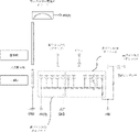
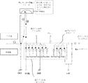
ここで、図1Aおよび図1Bを参照すると、本発明の例示的な装置が非常に図式的な形態で示されている。この実施形態では、陽イオンは、装置の入力開口部を通過するように、四重極によって加速および集束される。イオンは、次いで、二次電子(またはイオン)を放出する高エネルギー変換ダイノードに進む。変換ダイノードの湾曲した放出表面は、二次電子(またはイオン)を電子増倍器内、最初に左端のダイノード(電子増倍器の低ゲイン区分の第1のダイノードと見なされる)に集束させ、次いで、隣接するダイノードに偏向されたさらなる二次電子を放出し、次いで、(右の)隣接するダイノードに偏向されたさらなる二次電子を放出し、以下同様である。 1A and 1B, an exemplary apparatus of the present invention is shown in highly schematic form. In this embodiment, positive ions are accelerated and focused by a quadrupole so that they pass through the input aperture of the device. The ions then travel to a high energy conversion dynode that emits secondary electrons (or ions). The curved emitting surface of the conversion dynode focuses the secondary electrons (or ions) into the electron multiplier, first to the leftmost dynode (considered the first dynode in the low gain section of the electron multiplier); It then emits more secondary electrons deflected to the adjacent dynode, then more secondary electrons deflected to the adjacent (right) dynode, and so on.
引き続き図1Aおよび図1Bの実施形態によると、陽イオン検出のために、高エネルギー変換ダイノードは、高電圧バイアス-HV(B)を有する第1のダイノードの高電圧バイアスと比較して、より高い(または大幅により大きい大きさ、またはゼロからさらに離れた)高電圧バイアス-HV(A)を有することになる。陰イオンの検出のための電圧バイアスは、図2Bおよび図2Dに示されている。 Continuing with the embodiment of FIGS. 1A and 1B, for positive ion detection, the high energy conversion dynode has a higher voltage bias compared to the first dynode with a high voltage bias −HV(B). (or a significantly greater magnitude, or further away from zero) will have a high voltage bias -HV(A). Voltage biases for negative ion detection are shown in FIGS. 2B and 2D.
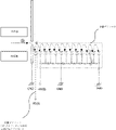
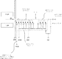
荷電粒子が本装置を通過する経路は、図2A、図2B、図2Cおよび図2Dに明確に示されている。 The paths taken by charged particles through the device are clearly shown in Figures 2A, 2B, 2C and 2D.
図2Aおよび図2Bの実施形態では、(左の低ゲイン区分の第1のダイノードから数えて)最初の5個のダイノードは、電子増倍器の低ゲイン部分を構成する。最初の3個のダイノードによって放出および増幅された電子から結果として生じる出力信号は、アナログである。 In the embodiment of Figures 2A and 2B, the first five dynodes (counting from the first dynode in the low gain section on the left) constitute the low gain portion of the electron multiplier. The output signal resulting from electrons emitted and amplified by the first three dynodes is analog.
第6および後続のダイノードは、電子増倍器の高ゲイン部分を構成する。第6および後続のダイノードによって放出および増幅された電子から結果として生じる出力信号は、(図示されないさらなる電子によって)計数出力を提供するために使用され得るパルス出力(デジタル)信号である。以下で論じられるように、装置の好ましい形態は、低ゲイン区分で12個のダイノード、高ゲイン区分で17個のダイノードなど、より多くのダイノード数を有する。 The sixth and subsequent dynodes constitute the high gain portion of the electron multiplier. The output signal resulting from electrons emitted and amplified by the sixth and subsequent dynodes is a pulsed output (digital) signal that can be used (by additional electrons not shown) to provide a counting output. As discussed below, the preferred form of the device has a higher dynode count, such as 12 dynodes in the low gain section and 17 dynodes in the high gain section.
図1Aおよび図1Bの好ましい実施形態では、変換ダイノードが、非常に大きい負電圧(-10kVなど)でバイアスされ、これが、入射イオンが正に帯電されている場合に必要とされることが留意されるであろう。当業者には理解されるように、入射イオンが負に帯電している場合、変換ダイノードは、非常に大きい正電圧(+10kVなど)でバイアスされる。高エネルギー変換ダイノードによって放出される粒子が負である場合(すなわち、電子)、電子増倍器の低ゲイン区分の第1のダイノードは、負(-2kVなど)である。入射イオンが負である場合、高エネルギー変換ダイノードは、衝突に対して陽イオンを放出し、第1のダイノードも負である(-2kVなど)。 Note that in the preferred embodiment of FIGS. 1A and 1B, the conversion dynode is biased with a very large negative voltage (such as −10 kV), which is required when the incident ions are positively charged. would be As will be appreciated by those skilled in the art, if the incident ions are negatively charged, the conversion dynode will be biased with a very large positive voltage (such as +10 kV). If the particles emitted by the high energy conversion dynodes are negative (ie electrons), the first dynode in the low gain section of the electron multiplier is negative (eg -2 kV). If the incident ions are negative, the high energy conversion dynode will emit positive ions upon collision and the first dynode will also be negative (eg -2 kV).
本発明によると、高エネルギー変換ダイノードが負電圧でバイアスされる場合、電子増倍器の低ゲイン区分の第1のダイノードは、より低い負電圧(すなわち、ゼロにより近い)でバイアスされる。高エネルギー変換ダイノードが正電圧でバイアスされる場合、電子増倍器の低ゲイン区分の第1のダイノードは、通常、負電圧でバイアスされる。 According to the present invention, when the high energy conversion dynode is biased with a negative voltage, the first dynode of the low gain section of the electron multiplier is biased with a lower negative voltage (ie closer to zero). If the high energy conversion dynode is biased with a positive voltage, the first dynode of the low gain section of the electron multiplier is normally biased with a negative voltage.
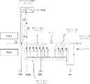
図1B、図2Cおよび図2Dから理解されるように、図1A、図2A、および図2Bに示される高エネルギー変換ダイノードの機能は、電子増倍器内またはその周りに物理的に位置付けられている変換ダイノードによって置き換えられ得る。これは、構築の容易さ、空間の節約という利点を提供し、さらに、組み合わせられた変換器/増倍器が使用され得、それによって部品交換のいかなる困難さも最小限に抑えることを提供する。電子増倍器内またはその周りに物理的に位置付けられた変換ダイノードを有する実施形態に関して、変換ダイノードには、相対的に中程度の電圧バイアス(約5、4、3、2、または1kV未満など)が印加されてもよい。一般に、約3kV未満の変換ダイノード電圧バイアスは、増倍器機能にいかなる実質的な悪影響も与えずに、変換ダイノードを電子増倍器に物理的に近接させることを可能にする。 As will be appreciated from FIGS. 1B, 2C and 2D, the function of the high energy conversion dynodes shown in FIGS. can be replaced by a conversion dynode with This provides the advantages of ease of construction, space savings, and further provides that a combined converter/multiplier can be used, thereby minimizing any difficulty in part replacement. For embodiments having conversion dynodes physically located within or around the electron multiplier, the conversion dynodes are subject to relatively moderate voltage biases (such as less than about 5, 4, 3, 2, or 1 kV). ) may be applied. Generally, a conversion dynode voltage bias of less than about 3 kV allows physical proximity of the conversion dynode to the electron multiplier without any substantial adverse effect on the multiplier function.
図1Cから理解されるように、装置のいくつかの実施形態の電子増倍器区分は、単一のゲイン増倍器である。そのような状況では、電子増倍器の全てのダイノードは、本明細書に開示された他の実施形態の高ゲイン区分および低ゲイン区分とは異なる、単一のゲイン区分を形成する。図1Cの実施形態では、利点は、(i)電子増倍器内に物理的に配設され、かつ(ii)電子増倍器から別個に電力供給されるか、または電気的に連結解除されている、変換ダイノードによって得られる。 As can be seen from FIG. 1C, the electron multiplier section of some embodiments of the device is a single gain multiplier. In such a situation, all dynodes of the electron multiplier form a single gain section as distinct from the high and low gain sections of other embodiments disclosed herein. In the embodiment of FIG. 1C, the advantage is (i) physically located within the electron multiplier and (ii) separately powered or electrically decoupled from the electron multiplier. , obtained by a transformation dynode.
一態様では、本発明は、変換ダイノードおよび増倍器ダイノードのチェーンの両方を備える粒子検出装置(質量分析計など)での使用のための交換部品または交換可能部品をさらに提供し、交換部品または交換可能部品は、変換ダイノードが増倍器ダイノードのチェーンとは別々に電力供給されることを可能にするように構成される。 In one aspect, the invention further provides a replacement or replaceable part for use in a particle detection device (such as a mass spectrometer) comprising both a conversion dynode and a chain of multiplier dynodes, The replaceable part is configured to allow the conversion dynodes to be powered separately from the chain of multiplier dynodes.
電子増倍器の電気抵抗(すなわち、高感度区分および低感度区分の組み合わせ)は、先行技術の電子検出器で知られている電気抵抗より低いレベル、かつ電子増倍器のダイナミックレンジが向上されるように、設定される。 The electrical resistance of the electron multiplier (i.e., the combination of the high sensitivity section and the low sensitivity section) is at a level lower than that known in prior art electron detectors, and the dynamic range of the electron multiplier is improved. is set as follows.
内部抵抗の低下に追加的もしくは代替的に、または内部抵抗の低下の自然な結果として、装置は、電子増倍器の高感度区分および低感度区分が少なくとも約50、75または100μAの線形出力電流で動作可能であるように構成される。電子増倍器の高感度区分および低感度区分の両方に関して、これは、先行技術の装置で利用される電流に対して約10倍の増加を表す。 Additionally or alternatively, or as a natural result of the reduction in internal resistance, the device provides a linear output current of at least about 50, 75 or 100 μA in the sensitive and insensitive sections of the electron multiplier. configured to be operable with For both the high-sensitivity and low-sensitivity sections of the electron multiplier, this represents an approximately ten-fold increase over the current utilized in prior art devices.
様々なダイノードを流れる差動電流が必要とされる場合、選択したダイノードに異なる大きさのバイアス電圧を印加するように構成された別々の電源の使用が、差動電流を達成する1つの手段であることに留意されたい。 If differential current through the various dynodes is required, the use of separate power supplies configured to apply bias voltages of different magnitudes to selected dynodes is one means of achieving the differential current. Note one thing.
理論によって限定されることを決して望むものではないが、検出器のダイナミックレンジが、低ゲイン区分および高ゲイン区分のダイナミックレンジの積であるため、検出器のダイナミックレンジの全体的な増加は、いくつかの実施形態では、典型的な市販の検出器よりも少なくとも1桁または2桁大きい場合がある。 While not wishing in any way to be bound by theory, since the dynamic range of a detector is the product of the dynamic ranges of the low-gain section and the high-gain section, the overall increase in detector dynamic range is In some embodiments, it may be at least one or two orders of magnitude greater than typical commercial detectors.
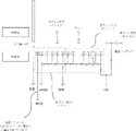
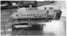
ここで、図1Aのスキームに従って広範に構成された本発明のプロトタイプ装置を示す、図3を参照する。高エネルギー変換ダイノードは、100で示され、電子増倍器は、110で示されている。電子増倍器110は、約120の低ゲイン部分および約130の高ゲイン部分を有する。
Reference is now made to FIG. 3, which shows a prototype device of the present invention broadly configured according to the scheme of FIG. 1A. A high energy conversion dynode is indicated at 100 and an electron multiplier is indicated at 110 . The
ここで図4を参照すると、本発明の装置の特定の動作パラメータがモデリングを介して推定されている。 Referring now to FIG. 4, certain operating parameters of the device of the present invention have been estimated via modeling.
理論によって限定されることを決して望むものではないが、ダイナミックレンジが、検出器の内部抵抗を低下させることによって向上され得ることが提案される。パルス計数区分(すなわち、高感度区分)およびアナログ区分(すなわち、低感度区分)は、両方とも少なくとも50uAの線形出力電流で動作するように設計される。各区分に関して、これは、市販されている典型的な先行技術の検出器よりも、およそ1桁大きい。 While not wishing in any way to be bound by theory, it is proposed that the dynamic range can be improved by lowering the internal resistance of the detector. Both the pulse counting section (ie, high sensitivity section) and the analog section (ie, low sensitivity section) are designed to operate with a linear output current of at least 50uA. For each segment, this is approximately an order of magnitude greater than typical prior art detectors on the market.
検出器のダイナミックレンジが、アナログ区分およびパルス計数区分のダイナミックレンジの積であるため、新しい検出器のダイナミックレンジの全体的な増加は、原理的には、典型的な市販の検出器よりも2桁大きい。 Since the dynamic range of the detector is the product of the dynamic ranges of the analog section and the pulse counting section, the overall increase in dynamic range of the new detector can in principle be 2x over typical commercial detectors. orders of magnitude larger.
装置の耐用年数、ゲイン安定性、差の比率の低下を向上させるために、ダイノード数が、各区分で増加しており、12個のダイノードがアナログ(すなわち、低感度)区分で使用され、17個のダイノードがパルス計数(すなわち、高感度)区分で使用された。 The number of dynodes was increased in each section to improve device lifetime, gain stability, and decrease in difference ratio, with 12 dynodes being used in the analog (i.e., low sensitivity) section and 17 dynodes were used in the pulse counting (ie high sensitivity) section.
別々に電源供給される変換ダイノードを使用する利点は、検出器の余分の耐用年数が提供されることであると期待されている。上述のように、誘導結合質量分析などの用途に使用される先行技術の検出器では、アナログ区分の開始電圧(-HV)は、通常、イオンから電子への適切な変換効率を確保するために、約-1600Vまで上げられる。高エネルギー変換ダイノードの導入によって、変換ダイノード電圧は、アナログゲインを提供するために必要とされる電圧から分離され得る。その結果、増倍器のアナログ区分は、はるかに低い初期-HV電圧で動作され得、それによってより長い耐用年数のために余分な電圧オーバーヘッドを提供する。 An advantage of using separately powered conversion dynodes is expected to be that extra detector life is provided. As noted above, in prior art detectors used for applications such as inductively coupled mass spectrometry, the starting voltage (−HV) of the analog section is usually set to , up to about -1600V. With the introduction of high energy conversion dynodes, the conversion dynode voltage can be separated from the voltage required to provide analog gain. As a result, the analog section of the multiplier can be operated at a much lower initial -HV voltage, thereby providing extra voltage overhead for longer service life.
入射イオンの検出効率に関しては、高速イオンが表面に入射するとき、二次電子がポアソン分布に従って放出され、イオンの質量およびエネルギー、ならびに放出表面の材料にも依存する平均を有する。二次イオン収率は、放出されたイオンの数のポアソン分布の平均に対応する。図5Aの傾向および値は、ステンレス鋼およびマグネシウム/銀変換ダイノードから予期され得るものの典型である。 Regarding incident ion detection efficiency, when a fast ion strikes a surface, secondary electrons are emitted according to a Poisson distribution, with an average that also depends on the mass and energy of the ion and the material of the emitting surface. The secondary ion yield corresponds to the mean of the Poisson distribution of the number of ions emitted. The trends and values in FIG. 5A are typical of what can be expected from stainless steel and magnesium/silver conversion dynodes.
イオン電子変換プロセスから放出された電子のポアソン分布は、電子増倍器からのパルス波高分布(PHD)の形状の決定要因であり、検出効率にも基本的な制限を課す。 The Poisson distribution of electrons emitted from the ion-to-electron conversion process determines the shape of the pulse height distribution (PHD) from the electron multiplier and also imposes fundamental limits on detection efficiency.
低平均値を有する二次電子放出分布に関して、イオンが変換表面に入射したときに、ゼロ電子が放出される確率が高い。 For a secondary electron emission distribution with a low average value, there is a high probability that zero electrons are emitted when an ion impinges on the conversion surface.
平均=0.8の分布に関して、~0.45の確率でゼロの二次電子が放出され(図5Bを参照)、すなわち、平均二次電子収率=0.8を有する種の最大可能な検出効率は、約55%である。収率=2を有する種に関して、ゼロの二次電子の確率は、約0.14まで低下し、最大可能な検出効率を約86%まで向上させる。 For a mean=0.8 distribution, zero secondary electrons are emitted with a probability of ˜0.45 (see FIG. 5B), i.e. the maximum possible Detection efficiency is about 55%. For species with yield=2, the zero secondary electron probability drops to about 0.14, improving the maximum possible detection efficiency to about 86%.
収率が4まで増加したとき、98%の検出効率が結果として得られる場合があり、そのような効率は、特に、低濃度の標的イオンが試料中に存在する場合に非常に望ましい。4の収率は、高エネルギー変換ダイノードの組み込みによって達成可能である。これは、電子増倍器の低ゲイン領域の第1のダイノードの前に高エネルギー変換ダイノードが配設されていない比較検出器で達成可能な検出効率における利点を提供する。 When the yield increases to 4, a detection efficiency of 98% may result, which is highly desirable, especially when low concentrations of target ions are present in the sample. Yields of 4 are achievable through the incorporation of high energy conversion dynodes. This provides an advantage in detection efficiency achievable with a comparison detector in which no high energy conversion dynode is placed before the first dynode in the low gain region of the electron multiplier.
所与の衝突エネルギーに対して、質量による二次電子収率の変動は、スペクトル内の質量バイアスにつながる。図5Aに示されるデータは、2keVの衝突エネルギーについて、二次電子収率が最大約2から最小約0.8まで変動することを示す。つまり、最大収率(5amuにおける)は、最小収率(140amuにおける)より約2.5倍高い。10keVの衝突エネルギーに関して、二次電子収率は、最大約5.1から最小約4.2まで変動する。この場合、最大収率は、最小収率より約1.2倍高いに過ぎない。 For a given collision energy, variations in secondary electron yield with mass lead to mass biases in the spectrum. The data shown in FIG. 5A show that the secondary electron yield varies from a maximum of about 2 to a minimum of about 0.8 for a collision energy of 2 keV. Thus, the maximum yield (at 5 amu) is approximately 2.5 times higher than the minimum yield (at 140 amu). For a collision energy of 10 keV, the secondary electron yield varies from a maximum of about 5.1 to a minimum of about 4.2. In this case the maximum yield is only about 1.2 times higher than the minimum yield.
140amuイオンの約4.2の二次電子収率を有する増倍器から同じまたは同様のレベルの信号を得るためには、140amuイオンの約0.8の収率を有する増倍器は、その検出器よりも約5.2倍(=4.2/0.8)高いゲインで動作する必要がある。より高いゲインで動作する必要性は、検出器の耐用年数を短縮させる場合があり、これは、本装置と比較したときの先行技術の検出器の欠点である。 To obtain the same or similar level of signal from a multiplier with a secondary electron yield of about 4.2 for 140 amu ions, a multiplier with a yield of about 0.8 for 140 amu ions would have It needs to operate at a gain about 5.2 times (=4.2/0.8) higher than the detector. The need to operate at higher gains may shorten the useful life of the detector, which is a drawback of prior art detectors when compared to the present device.
プロトタイプの線形性レベルが測定され得る。3e3のゲインで50uAのアナログ出力電流を得るために、約16nAを超える入力イオン電流が必要とされる。この大きさのイオン電流は、例えば、質量分析器具から取得可能である。 The linearity level of the prototype can be measured. To obtain an analog output current of 50uA with a gain of 3e3, an input ion current of more than about 16nA is required. An ion current of this magnitude is obtainable, for example, from a mass spectrometry instrument.
ゲイン曲線は、図3に示されるプロトタイプ検出器の低ゲイン(アナログ)区分(図6A参照)および高ゲイン(パルス計数)区分(図6B参照)に関して生成されている。約3e3のアナログゲインを得るために、約1100Vの開始電圧が必要とされる。これは、ICP-MS検出器のアナログ区分に通常印加される開始電圧よりも約500V低い。 Gain curves are generated for the low gain (analog) section (see FIG. 6A) and the high gain (pulse counting) section (see FIG. 6B) of the prototype detector shown in FIG. To obtain an analog gain of about 3e3, a starting voltage of about 1100V is required. This is about 500V lower than the starting voltage normally applied to the analog section of the ICP-MS detector.
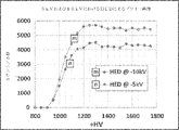
有利なことに、図3に示されるプロトタイプ検出器は、-5kVまたは-10kVが高エネルギー変換ダイノードに印加された状態で、高品質プラトー曲線を生成することが実証されている(図5参照)。これは、変換ダイノードからの増加した二次電子収率に起因して改善されたパルス波高分布を表している。高品質プラトー曲線は、パルス計数動作電圧の信頼性のある設定を可能にする。 Advantageously, the prototype detector shown in FIG. 3 has been demonstrated to produce high quality plateau curves with −5 kV or −10 kV applied to the high energy conversion dynodes (see FIG. 5). . This represents an improved pulse height distribution due to increased secondary electron yield from the conversion dynode. A high quality plateau curve allows reliable setting of the pulse counting operating voltage.
動作における任意の機能の改善とはまったく別に、別個の高エネルギー変換ダイノードの組み込みは、検出器の機械設計に柔軟性を提供する。いくつかの実施形態では、電子増倍器は、変換ダイノード上の任意の方向に回転され得、それによって四重極に対する軸方向または半径方向の配向を可能にする。高感度区分および低感度区分を有する別個のダイノード電子増倍器110と動作可能に接続されている高エネルギー変換ダイノード100を有するプロトタイプ検出器を示す、図3を参照する。
Quite apart from any functional improvements in operation, the incorporation of separate high energy conversion dynodes provides flexibility in the mechanical design of the detector. In some embodiments, the electron multiplier can be rotated in any direction on the conversion dynode, thereby allowing axial or radial orientation with respect to the quadrupole. Reference is made to FIG. 3, which shows a prototype detector having a high
本装置は、非常に低含量のイオンが検出されることを必要とする用途で使用される器具を含む、質量分析器具の検出器構成要素として特に有用である。そのような用途としては、誘導結合質量分析が挙げられる。したがって、一態様では、本発明は、本明細書に説明されるように、誘導結合質量分析器具および装置の組み合わせを提供する。 The device is particularly useful as a detector component of mass spectrometry instruments, including instruments used in applications requiring very low abundance ions to be detected. Such applications include inductively coupled mass spectrometry. Accordingly, in one aspect, the invention provides a combination of inductively coupled mass spectrometry instruments and devices as described herein.
器具は、誘導結合プラズマによって試料をイオン化する手段を備え得る。 The instrument may comprise means for ionizing the sample by means of an inductively coupled plasma.
誘導結合プラズマは、電磁コイルでガスを加熱することによって一般に生成されるプラズマであり、ガスは、それを導電性にするために十分な濃度のイオンおよび電子を含有している。プラズマは、3つの同心円管(通常は石英)からなる器具のトーチで一般に維持され、トーチの端は、誘導コイルの内側に配設されている。器具は、通常、トーチの最も外側の2つの管の間にアルゴンを導入する手段を備え、電気火花が断続的に印加されて、自由電子をガス流内に導入する。電子は、加速され、アルゴン原子と衝突して、次に加速される電子の放出を引き起こし得る。プロセスは、衝突における新しい電子の放出速度が、アルゴンイオン(電子を失った原子)との電子の再結合の速度と平衡されるまで続く。プラズマの温度は、約10,000Kである。 An inductively coupled plasma is a plasma generally produced by heating a gas with an electromagnetic coil, the gas containing sufficient concentrations of ions and electrons to make it conductive. The plasma is generally maintained in an instrument torch consisting of three concentric tubes (usually quartz) with the ends of the torch positioned inside an induction coil. The instrument usually comprises means for introducing argon between the two outermost tubes of the torch and an electrical spark is applied intermittently to introduce free electrons into the gas stream. Electrons can be accelerated and collide with argon atoms, causing the emission of in turn accelerated electrons. The process continues until the rate of emission of new electrons in collisions is balanced with the rate of recombination of electrons with argon ions (atoms that have lost electrons). The temperature of the plasma is approximately 10,000K.
本装置は、既存の市販されているICP-MS器具動作可能となるように物理的および/または構造的に構成され得る。単に例として、本装置は、モデル7800、7900、8900Triple Quadrupole、8800Triple Quadrupole、7700e、7700x、および7700sなどのAgilent(商標)、またはモデルNexION2000、N8150045、N8150044、N8150046、およびN8150047などのPerkinElmer(商標)、またはThermoFisher ScientificのモデルiCAP RQ、iCAP TQ、およびElement Seriesなど、またはShimadzuのモデルICPMS-2030などによって提供されるICP-MS器具のいずれかで電子増倍器として動作可能であるように構成され得る。 The device may be physically and/or structurally configured to be operable with existing commercially available ICP-MS instruments. By way of example only, the instrument may be used with Agilent™ models such as Models 7800, 7900, 8900 Triple Quadrupole, 8800 Triple Quadrupole, 7700e, 7700x, and 7700s, or Models NexION2000, N8150045, N8150044, N8150150, N8150150, N8150150, N8150150, and N8150150. , or ICP-MS instruments such as those provided by ThermoFisher Scientific models iCAP RQ, iCAP TQ, and Element Series, or Shimadzu model ICPMS-2030. obtain.
本装置の電子増倍器構成要素は、線形の別個のダイノード増倍器によって例示されてきた。本明細書の利点を考慮すると、当業者は、本発明との適合性について他のタイプの増倍器タイプを常習的に試験することが可能である。例えば、連続(チャネル)ダイノードが、別個のダイノード電子増倍器の代わりに使用され得る。その場合、装置は、連続ダイノードと組み合わせて高エネルギー変換ダイノードを備え得る。 The electron multiplier component of the device has been exemplified by a linear discrete dynode multiplier. Given the benefit of this specification, those skilled in the art can routinely test other types of multiplier types for compatibility with the present invention. For example, continuous (channel) dynodes can be used instead of separate dynode electron multipliers. In that case, the apparatus may comprise high energy conversion dynodes in combination with continuous dynodes.
さらに、本装置は、ICP-MS器具およびその構成要素に関して特に有利であるが、本出願の範囲がそのように制限されることを意図するものではない。本発明の少なくともいくつかの特徴は、非ICP-MS器具およびその構成要素に適用され得ることが企図される。例えば、電子増倍器での高ゲイン区分および低ゲイン区分のダイノードの使用は、それにもかかわらず、電子増倍器の構造内への別々に電力供給される変換ダイノードの統合と同様に、利点を提供し得る。当業者は、常習的方法を使用して、様々な既存の質量分析器具およびその構成要素に関して、さらには質量分析に関係ない用途についても、本発明の有用性を試験することができる。 Moreover, although the device is particularly advantageous with respect to ICP-MS instruments and components thereof, the scope of the present application is not intended to be so limited. It is contemplated that at least some features of the invention may be applied to non-ICP-MS instruments and components thereof. For example, the use of high-gain section and low-gain section dynodes in an electron multiplier nevertheless has advantages, as does the integration of separately powered conversion dynodes within the structure of the electron multiplier. can provide One skilled in the art can use routine methods to test the utility of the present invention with respect to a variety of existing mass spectrometry instruments and their components, as well as for applications not related to mass spectrometry.
本発明の例示的な実施形態の説明では、本発明の様々な特徴は、開示を合理化し、様々な発明の態様のうちの1つ以上の理解を助ける目的で、単一の実施形態、図、またはその説明にまとめられている場合があることが理解されるであろう。しかしながら、この開示方法は、特許請求の範囲の発明が各請求項に明示的に列挙されているよりも多くの特徴を必要とするという意図を反映するものとして解釈されるべきではない。むしろ、以下の特許請求の範囲が反映するように、発明の態様は、単一の上述の開示された実施形態の全ての特徴であるとはいえない。 In describing illustrative embodiments of the invention, various features of the invention are presented in the context of a single embodiment, diagrammatic representation, for the purpose of streamlining the disclosure and aiding in understanding one or more of the various inventive aspects. , or summarized in the description thereof. This method of disclosure, however, is not to be interpreted as reflecting an intention that the claimed invention requires more features than are expressly recited in each claim. Rather, as the following claims reflect, inventive aspects lie in less than all features of a single foregoing disclosed embodiment.
さらに、本明細書に説明されるいくつかの実施形態は、他の実施形態に含まれる特徴のいくつかを含むが、他の特徴を含まず、さらに、当業者によって理解されるように、異なる実施形態の特徴の組み合わせは、本発明の範囲内にあり、異なる実施形態を形成することを意味する。例えば、以下の特許請求の範囲では、特許請求の範囲の実施形態のいずれも、任意の組み合わせで使用することができる。 Moreover, some embodiments described herein may include some of the features contained in other embodiments, but not others, and may also include different features, as will be appreciated by those skilled in the art. Combinations of features of the embodiments are meant to form different embodiments within the scope of the invention. For example, in the following claims, any of the claim embodiments can be used in any combination.
本明細書で提供される説明では、多数の特定の詳細が示されている。しかしながら、本発明の実施形態は、これらの特定の詳細なしで実施され得ることが理解される。他の事例では、周知の方法、構造および技術は、本説明の理解を不明瞭にしないために、詳細に示されていない。 Numerous specific details are given in the description provided herein. However, it is understood that embodiments of the invention may be practiced without these specific details. In other instances, well-known methods, structures and techniques have not been shown in detail so as not to obscure the understanding of this description.
したがって、本発明の好ましい実施形態であると考えられるものを説明してきたが、当業者は、他のおよびさらなる修正が、本発明の主旨から逸脱せずに、それらになされ得ることを認識することになり、全てのそのような変更および修正が本発明の範囲内に収まるように主張することが意図される。機能が図に追加または削除されてもよく、動作が、機能ブロック間で交換されてもよい。ステップが、本発明の範囲内で説明される方法に追加または削除されてもよい。 Thus, having described what are believed to be the preferred embodiments of the invention, those skilled in the art will recognize that other and further modifications can be made thereto without departing from the spirit of the invention. and all such changes and modifications are intended to be claimed as coming within the scope of the present invention. Functionality may be added or deleted from the diagrams and operations may be interchanged between functional blocks. Steps may be added or deleted from methods described within the scope of the present invention.
本発明が特定の例を参照して説明されたが、本発明が多くの他の形態で実施され得ることが当業者によって理解されるであろう。 Although the invention has been described with reference to specific examples, it will be appreciated by those skilled in the art that the invention may be embodied in many other forms.
Claims (18)
粒子による衝突時に1つ以上の二次電子またはイオンを放出するように構成された変換ダイノードと、
前記変換ダイノードによって放出される前記1つ以上の二次電子またはイオンから増幅された電子信号出力を形成するように構成された電子増倍器と、を備えており、
前記電子増倍器が、相対的低感度区分および相対的高感度区分を有しており、前記変換ダイノードは、前記相対的低感度区分とは電気的に連結解除されている、装置。 A device for detecting charged particles, comprising:
a conversion dynode configured to emit one or more secondary electrons or ions upon impact with a particle;
an electron multiplier configured to form an amplified electronic signal output from the one or more secondary electrons or ions emitted by the conversion dynode;
The apparatus of claim 1, wherein the electron multiplier has a relatively low sensitivity section and a relatively high sensitivity section, the conversion dynode being electrically decoupled from the relatively low sensitivity section.
Applications Claiming Priority (4)
| Application Number | Priority Date | Filing Date | Title |
|---|---|---|---|
| US201762514029P | 2017-06-02 | 2017-06-02 | |
| US62/514,029 | 2017-06-02 | ||
| JP2019561270A JP2020522087A (en) | 2017-06-02 | 2018-06-01 | Improved charged particle detector |
| PCT/AU2018/050545 WO2018218308A1 (en) | 2017-06-02 | 2018-06-01 | Improved charged particle detector |
Related Parent Applications (1)
| Application Number | Title | Priority Date | Filing Date |
|---|---|---|---|
| JP2019561270A Division JP2020522087A (en) | 2017-06-02 | 2018-06-01 | Improved charged particle detector |
Publications (2)
| Publication Number | Publication Date |
|---|---|
| JP2022166330A true JP2022166330A (en) | 2022-11-01 |
| JP7433390B2 JP7433390B2 (en) | 2024-02-19 |
Family
ID=64454261
Family Applications (2)
| Application Number | Title | Priority Date | Filing Date |
|---|---|---|---|
| JP2019561270A Pending JP2020522087A (en) | 2017-06-02 | 2018-06-01 | Improved charged particle detector |
| JP2022135958A Active JP7433390B2 (en) | 2017-06-02 | 2022-08-29 | Improved charged particle detector |
Family Applications Before (1)
| Application Number | Title | Priority Date | Filing Date |
|---|---|---|---|
| JP2019561270A Pending JP2020522087A (en) | 2017-06-02 | 2018-06-01 | Improved charged particle detector |
Country Status (8)
| Country | Link |
|---|---|
| US (1) | US12224170B2 (en) |
| EP (1) | EP3631841A4 (en) |
| JP (2) | JP2020522087A (en) |
| KR (1) | KR20200014804A (en) |
| CN (1) | CN110832615B (en) |
| AU (1) | AU2018276071A1 (en) |
| CA (1) | CA3065324A1 (en) |
| WO (1) | WO2018218308A1 (en) |
Families Citing this family (7)
| Publication number | Priority date | Publication date | Assignee | Title |
|---|---|---|---|---|
| US10784095B2 (en) | 2018-12-18 | 2020-09-22 | Thermo Finnigan Llc | Multidimensional dynode detector |
| JP7168542B2 (en) * | 2019-10-18 | 2022-11-09 | 株式会社日立ハイテク | Power module and mass spectrometer |
| US11469091B1 (en) | 2021-04-30 | 2022-10-11 | Perkinelmer Health Sciences Canada, Inc. | Mass spectrometer apparatus including ion detection to minimize differential drift |
| US20240258089A1 (en) * | 2021-05-31 | 2024-08-01 | Adaptas Solutions Pty Ltd | Electron Multiplier Having Improved Voltage Stabilisation |
| CN115938907A (en) * | 2021-10-06 | 2023-04-07 | 萨默费尼根有限公司 | High-speed polarity-switching double-conversion dynode ion detector for mass spectrometers |
| CN114758943B (en) * | 2022-04-15 | 2025-05-23 | 国科新智(天津)科技发展有限公司 | Signal detection circuit of electron multiplier |
| JP7786296B2 (en) | 2022-04-26 | 2025-12-16 | 株式会社島津製作所 | mass spectrometer |
Citations (4)
| Publication number | Priority date | Publication date | Assignee | Title |
|---|---|---|---|---|
| JPS6316233A (en) * | 1986-07-09 | 1988-01-23 | Rigaku Keisoku Kk | Driving device for secondary electron multiplier |
| US5463219A (en) * | 1994-12-07 | 1995-10-31 | Mds Health Group Limited | Mass spectrometer system and method using simultaneous mode detector and signal region flags |
| US20110001043A1 (en) * | 2008-01-04 | 2011-01-06 | Covalx Ag | Detector device for high mass ion detection, a method for analyzing ions of high mass and a device for selection between ion detectors |
| US20150162174A1 (en) * | 2013-11-26 | 2015-06-11 | Perkinelmer Health Sciences, Inc. | Detectors and methods of using them |
Family Cites Families (12)
| Publication number | Priority date | Publication date | Assignee | Title |
|---|---|---|---|---|
| US3898456A (en) * | 1974-07-25 | 1975-08-05 | Us Energy | Electron multiplier-ion detector system |
| JPH083987B2 (en) * | 1989-01-09 | 1996-01-17 | 株式会社日立製作所 | Post-stage acceleration detector for mass spectrometer |
| US5374827A (en) * | 1993-11-15 | 1994-12-20 | Detector Technology, Inc. | Bias for a conversion dynode in an electron multiplier |
| AUPR455801A0 (en) | 2001-04-24 | 2001-05-24 | Varian Australia Pty Ltd | Voltage divider circuit for an electron multiplier |
| US7109463B2 (en) * | 2002-07-29 | 2006-09-19 | Applied Materials, Inc. | Amplifier circuit with a switching device to provide a wide dynamic output range |
| US6707034B1 (en) | 2002-08-29 | 2004-03-16 | Hamamatsu Photonics K.K. | Mass spectrometer and ion detector used therein |
| US8735818B2 (en) | 2010-03-31 | 2014-05-27 | Thermo Finnigan Llc | Discrete dynode detector with dynamic gain control |
| US8530829B2 (en) * | 2010-09-23 | 2013-09-10 | Agilent Technologies, Inc. | Inductively coupled plasma mass spectroscopy apparatus and measured data processing method in the inductively coupled plasma mass spectroscopy apparatus |
| GB2486484B (en) * | 2010-12-17 | 2013-02-20 | Thermo Fisher Scient Bremen | Ion detection system and method |
| CN104011829A (en) * | 2011-12-27 | 2014-08-27 | Dh科技发展私人贸易有限公司 | Ultrafast transimpedance amplifier interfacing electron multipliers for pulse counting applications |
| WO2014045360A1 (en) | 2012-09-20 | 2014-03-27 | 株式会社島津製作所 | Mass spectrometer |
| JP6272028B2 (en) | 2013-12-27 | 2018-01-31 | アジレント・テクノロジーズ・インクAgilent Technologies, Inc. | Secondary electron multiplier for mass spectrometer |
-
2018
- 2018-06-01 WO PCT/AU2018/050545 patent/WO2018218308A1/en not_active Ceased
- 2018-06-01 KR KR1020197038057A patent/KR20200014804A/en not_active Withdrawn
- 2018-06-01 EP EP18809917.0A patent/EP3631841A4/en active Pending
- 2018-06-01 US US16/617,963 patent/US12224170B2/en active Active
- 2018-06-01 CA CA3065324A patent/CA3065324A1/en active Pending
- 2018-06-01 AU AU2018276071A patent/AU2018276071A1/en not_active Abandoned
- 2018-06-01 JP JP2019561270A patent/JP2020522087A/en active Pending
- 2018-06-01 CN CN201880035699.1A patent/CN110832615B/en active Active
-
2022
- 2022-08-29 JP JP2022135958A patent/JP7433390B2/en active Active
Patent Citations (4)
| Publication number | Priority date | Publication date | Assignee | Title |
|---|---|---|---|---|
| JPS6316233A (en) * | 1986-07-09 | 1988-01-23 | Rigaku Keisoku Kk | Driving device for secondary electron multiplier |
| US5463219A (en) * | 1994-12-07 | 1995-10-31 | Mds Health Group Limited | Mass spectrometer system and method using simultaneous mode detector and signal region flags |
| US20110001043A1 (en) * | 2008-01-04 | 2011-01-06 | Covalx Ag | Detector device for high mass ion detection, a method for analyzing ions of high mass and a device for selection between ion detectors |
| US20150162174A1 (en) * | 2013-11-26 | 2015-06-11 | Perkinelmer Health Sciences, Inc. | Detectors and methods of using them |
Also Published As
| Publication number | Publication date |
|---|---|
| CN110832615B (en) | 2023-05-23 |
| JP2020522087A (en) | 2020-07-27 |
| US20200194246A1 (en) | 2020-06-18 |
| AU2018276071A1 (en) | 2019-10-31 |
| EP3631841A1 (en) | 2020-04-08 |
| CA3065324A1 (en) | 2018-12-06 |
| WO2018218308A1 (en) | 2018-12-06 |
| JP7433390B2 (en) | 2024-02-19 |
| US12224170B2 (en) | 2025-02-11 |
| KR20200014804A (en) | 2020-02-11 |
| EP3631841A4 (en) | 2021-03-03 |
| CN110832615A (en) | 2020-02-21 |
Similar Documents
| Publication | Publication Date | Title |
|---|---|---|
| JP7433390B2 (en) | Improved charged particle detector | |
| Aumayr et al. | On the measurement of statistics for particle-induced electron emission from a clean metal surface | |
| US10615019B2 (en) | Electron multiplier for mass spectrometer | |
| US7847268B2 (en) | Three modes particle detector | |
| US7728292B2 (en) | Method and apparatus for detecting positively charged and negatively charged ionized particles | |
| JP2015503824A (en) | Ultrafast transimpedance amplifier interacting with electron multiplier for pulse counting applications | |
| US7791020B2 (en) | Multistage gas cascade amplifier | |
| US6982428B2 (en) | Particle detection by electron multiplication | |
| JP2022103330A (en) | Improvements in photomultiplier tubes | |
| Stockli et al. | Analog gain of microchannel plates for 1.5–154 keV/q Ar q+ (3⩽ q⩽ 16) | |
| JP5175388B2 (en) | Ion detection device for mass spectrometry, ion detection method, and method of manufacturing ion detection device | |
| HK40016398A (en) | Improved charged particle detector | |
| JPH07192687A (en) | Ion detection method, mass spectrometry method, ion detection apparatus, and mass spectrometry apparatus | |
| JP5215569B2 (en) | Channel type electron multiplier | |
| US20230015584A1 (en) | Instruments including an electron multiplier | |
| AU2017203761A1 (en) | Improved charged particle detector | |
| Almen et al. | Fast rise time, high sensitivity MCP ion detector for low-energy ion spectroscopy | |
| US3413479A (en) | Radiation detector and amplifier having an input axial slot | |
| TWI441230B (en) | Particle detection system and electron beam | |
| Zhang et al. | A new method of measuring electron emission induced by low energy ions from solids | |
| WO2010125671A1 (en) | Secondary electron multiplier, ion detection device, and ion detection method | |
| HK40001500A (en) | Improvements in electron multipliers |
Legal Events
| Date | Code | Title | Description |
|---|---|---|---|
| A621 | Written request for application examination |
Free format text: JAPANESE INTERMEDIATE CODE: A621 Effective date: 20220829 |
|
| A977 | Report on retrieval |
Free format text: JAPANESE INTERMEDIATE CODE: A971007 Effective date: 20230511 |
|
| A131 | Notification of reasons for refusal |
Free format text: JAPANESE INTERMEDIATE CODE: A131 Effective date: 20230523 |
|
| A521 | Request for written amendment filed |
Free format text: JAPANESE INTERMEDIATE CODE: A523 Effective date: 20230818 |
|
| A131 | Notification of reasons for refusal |
Free format text: JAPANESE INTERMEDIATE CODE: A131 Effective date: 20230829 |
|
| A601 | Written request for extension of time |
Free format text: JAPANESE INTERMEDIATE CODE: A601 Effective date: 20231128 |
|
| A521 | Request for written amendment filed |
Free format text: JAPANESE INTERMEDIATE CODE: A523 Effective date: 20231222 |
|
| TRDD | Decision of grant or rejection written | ||
| A01 | Written decision to grant a patent or to grant a registration (utility model) |
Free format text: JAPANESE INTERMEDIATE CODE: A01 Effective date: 20240116 |
|
| A61 | First payment of annual fees (during grant procedure) |
Free format text: JAPANESE INTERMEDIATE CODE: A61 Effective date: 20240206 |
|
| R150 | Certificate of patent or registration of utility model |
Ref document number: 7433390 Country of ref document: JP Free format text: JAPANESE INTERMEDIATE CODE: R150 |