JP2022151587A - Self-aligned gate endcap (sage) architectures with reduced cap - Google Patents
Self-aligned gate endcap (sage) architectures with reduced cap Download PDFInfo
- Publication number
- JP2022151587A JP2022151587A JP2022004048A JP2022004048A JP2022151587A JP 2022151587 A JP2022151587 A JP 2022151587A JP 2022004048 A JP2022004048 A JP 2022004048A JP 2022004048 A JP2022004048 A JP 2022004048A JP 2022151587 A JP2022151587 A JP 2022151587A
- Authority
- JP
- Japan
- Prior art keywords
- gate
- dielectric
- gate electrode
- integrated circuit
- trench contact
- Prior art date
- Legal status (The legal status is an assumption and is not a legal conclusion. Google has not performed a legal analysis and makes no representation as to the accuracy of the status listed.)
- Pending
Links
- 235000002020 sage Nutrition 0.000 title 1
- 238000002955 isolation Methods 0.000 claims abstract description 123
- 239000004065 semiconductor Substances 0.000 claims abstract description 87
- 238000004891 communication Methods 0.000 claims description 20
- 230000015654 memory Effects 0.000 claims description 15
- 238000000034 method Methods 0.000 abstract description 95
- 238000004519 manufacturing process Methods 0.000 abstract description 31
- 239000010410 layer Substances 0.000 description 160
- 230000008569 process Effects 0.000 description 76
- 239000000463 material Substances 0.000 description 61
- 239000000758 substrate Substances 0.000 description 50
- 229910052751 metal Inorganic materials 0.000 description 47
- 239000002184 metal Substances 0.000 description 47
- VYPSYNLAJGMNEJ-UHFFFAOYSA-N Silicium dioxide Chemical compound O=[Si]=O VYPSYNLAJGMNEJ-UHFFFAOYSA-N 0.000 description 21
- 238000013459 approach Methods 0.000 description 20
- 125000006850 spacer group Chemical group 0.000 description 18
- 229910052581 Si3N4 Inorganic materials 0.000 description 16
- HQVNEWCFYHHQES-UHFFFAOYSA-N silicon nitride Chemical compound N12[Si]34N5[Si]62N3[Si]51N64 HQVNEWCFYHHQES-UHFFFAOYSA-N 0.000 description 16
- XUIMIQQOPSSXEZ-UHFFFAOYSA-N Silicon Chemical compound [Si] XUIMIQQOPSSXEZ-UHFFFAOYSA-N 0.000 description 15
- 239000003989 dielectric material Substances 0.000 description 15
- 229910052710 silicon Inorganic materials 0.000 description 14
- 239000010703 silicon Substances 0.000 description 14
- 238000009792 diffusion process Methods 0.000 description 12
- 238000000059 patterning Methods 0.000 description 12
- 238000005516 engineering process Methods 0.000 description 9
- 238000001459 lithography Methods 0.000 description 9
- 150000002739 metals Chemical class 0.000 description 8
- 235000012239 silicon dioxide Nutrition 0.000 description 8
- 239000000377 silicon dioxide Substances 0.000 description 8
- 229910052814 silicon oxide Inorganic materials 0.000 description 8
- 229910000449 hafnium oxide Inorganic materials 0.000 description 7
- WIHZLLGSGQNAGK-UHFFFAOYSA-N hafnium(4+);oxygen(2-) Chemical compound [O-2].[O-2].[Hf+4] WIHZLLGSGQNAGK-UHFFFAOYSA-N 0.000 description 7
- 230000009467 reduction Effects 0.000 description 7
- 229910045601 alloy Inorganic materials 0.000 description 6
- 239000000956 alloy Substances 0.000 description 6
- 238000000151 deposition Methods 0.000 description 6
- PXHVJJICTQNCMI-UHFFFAOYSA-N Nickel Chemical compound [Ni] PXHVJJICTQNCMI-UHFFFAOYSA-N 0.000 description 5
- 230000008901 benefit Effects 0.000 description 5
- 238000005229 chemical vapour deposition Methods 0.000 description 5
- RYGMFSIKBFXOCR-UHFFFAOYSA-N Copper Chemical group [Cu] RYGMFSIKBFXOCR-UHFFFAOYSA-N 0.000 description 4
- 239000006117 anti-reflective coating Substances 0.000 description 4
- 230000004888 barrier function Effects 0.000 description 4
- 230000015572 biosynthetic process Effects 0.000 description 4
- -1 but not limited to Substances 0.000 description 4
- 239000003990 capacitor Substances 0.000 description 4
- 229910052802 copper Inorganic materials 0.000 description 4
- 239000010949 copper Substances 0.000 description 4
- 238000005137 deposition process Methods 0.000 description 4
- 230000009977 dual effect Effects 0.000 description 4
- 229910052732 germanium Inorganic materials 0.000 description 4
- GNPVGFCGXDBREM-UHFFFAOYSA-N germanium atom Chemical compound [Ge] GNPVGFCGXDBREM-UHFFFAOYSA-N 0.000 description 4
- 229910052735 hafnium Inorganic materials 0.000 description 4
- 229910044991 metal oxide Inorganic materials 0.000 description 4
- 150000004706 metal oxides Chemical class 0.000 description 4
- 239000000203 mixture Substances 0.000 description 4
- 239000002070 nanowire Substances 0.000 description 4
- 238000005240 physical vapour deposition Methods 0.000 description 4
- LIVNPJMFVYWSIS-UHFFFAOYSA-N silicon monoxide Chemical class [Si-]#[O+] LIVNPJMFVYWSIS-UHFFFAOYSA-N 0.000 description 4
- KDLHZDBZIXYQEI-UHFFFAOYSA-N Palladium Chemical compound [Pd] KDLHZDBZIXYQEI-UHFFFAOYSA-N 0.000 description 3
- 229910000577 Silicon-germanium Inorganic materials 0.000 description 3
- 238000005520 cutting process Methods 0.000 description 3
- 230000008021 deposition Effects 0.000 description 3
- VBJZVLUMGGDVMO-UHFFFAOYSA-N hafnium atom Chemical group [Hf] VBJZVLUMGGDVMO-UHFFFAOYSA-N 0.000 description 3
- 238000004377 microelectronic Methods 0.000 description 3
- 229910052759 nickel Inorganic materials 0.000 description 3
- BASFCYQUMIYNBI-UHFFFAOYSA-N platinum Chemical compound [Pt] BASFCYQUMIYNBI-UHFFFAOYSA-N 0.000 description 3
- 229910021420 polycrystalline silicon Inorganic materials 0.000 description 3
- 229920005591 polysilicon Polymers 0.000 description 3
- 239000010936 titanium Substances 0.000 description 3
- OKTJSMMVPCPJKN-UHFFFAOYSA-N Carbon Chemical compound [C] OKTJSMMVPCPJKN-UHFFFAOYSA-N 0.000 description 2
- 229910005540 GaP Inorganic materials 0.000 description 2
- NBIIXXVUZAFLBC-UHFFFAOYSA-N Phosphoric acid Chemical compound OP(O)(O)=O NBIIXXVUZAFLBC-UHFFFAOYSA-N 0.000 description 2
- 229910052782 aluminium Inorganic materials 0.000 description 2
- 229910021417 amorphous silicon Inorganic materials 0.000 description 2
- 238000000137 annealing Methods 0.000 description 2
- 229910052799 carbon Inorganic materials 0.000 description 2
- 239000002800 charge carrier Substances 0.000 description 2
- 229910017052 cobalt Inorganic materials 0.000 description 2
- 239000010941 cobalt Substances 0.000 description 2
- GUTLYIVDDKVIGB-UHFFFAOYSA-N cobalt atom Chemical compound [Co] GUTLYIVDDKVIGB-UHFFFAOYSA-N 0.000 description 2
- 239000004020 conductor Substances 0.000 description 2
- 238000013461 design Methods 0.000 description 2
- 238000001312 dry etching Methods 0.000 description 2
- 239000003822 epoxy resin Substances 0.000 description 2
- 238000005530 etching Methods 0.000 description 2
- HZXMRANICFIONG-UHFFFAOYSA-N gallium phosphide Chemical compound [Ga]#P HZXMRANICFIONG-UHFFFAOYSA-N 0.000 description 2
- 230000006872 improvement Effects 0.000 description 2
- MRELNEQAGSRDBK-UHFFFAOYSA-N lanthanum(3+);oxygen(2-) Chemical compound [O-2].[O-2].[O-2].[La+3].[La+3] MRELNEQAGSRDBK-UHFFFAOYSA-N 0.000 description 2
- 230000000873 masking effect Effects 0.000 description 2
- 150000004767 nitrides Chemical class 0.000 description 2
- TWNQGVIAIRXVLR-UHFFFAOYSA-N oxo(oxoalumanyloxy)alumane Chemical compound O=[Al]O[Al]=O TWNQGVIAIRXVLR-UHFFFAOYSA-N 0.000 description 2
- RVTZCBVAJQQJTK-UHFFFAOYSA-N oxygen(2-);zirconium(4+) Chemical compound [O-2].[O-2].[Zr+4] RVTZCBVAJQQJTK-UHFFFAOYSA-N 0.000 description 2
- 229910052763 palladium Inorganic materials 0.000 description 2
- 229920002120 photoresistant polymer Polymers 0.000 description 2
- 229910052697 platinum Inorganic materials 0.000 description 2
- 229920000647 polyepoxide Polymers 0.000 description 2
- 238000012545 processing Methods 0.000 description 2
- 229910052707 ruthenium Inorganic materials 0.000 description 2
- 229910021332 silicide Inorganic materials 0.000 description 2
- WGTYBPLFGIVFAS-UHFFFAOYSA-M tetramethylammonium hydroxide Chemical compound [OH-].C[N+](C)(C)C WGTYBPLFGIVFAS-UHFFFAOYSA-M 0.000 description 2
- 229910052719 titanium Inorganic materials 0.000 description 2
- 229910052721 tungsten Inorganic materials 0.000 description 2
- 238000001039 wet etching Methods 0.000 description 2
- 229910052726 zirconium Inorganic materials 0.000 description 2
- 229910001928 zirconium oxide Inorganic materials 0.000 description 2
- 229910000951 Aluminide Inorganic materials 0.000 description 1
- VHUUQVKOLVNVRT-UHFFFAOYSA-N Ammonium hydroxide Chemical compound [NH4+].[OH-] VHUUQVKOLVNVRT-UHFFFAOYSA-N 0.000 description 1
- JBRZTFJDHDCESZ-UHFFFAOYSA-N AsGa Chemical compound [As]#[Ga] JBRZTFJDHDCESZ-UHFFFAOYSA-N 0.000 description 1
- 229910000952 Be alloy Inorganic materials 0.000 description 1
- ZOXJGFHDIHLPTG-UHFFFAOYSA-N Boron Chemical compound [B] ZOXJGFHDIHLPTG-UHFFFAOYSA-N 0.000 description 1
- 108700028490 CAP protocol 2 Proteins 0.000 description 1
- 229910002601 GaN Inorganic materials 0.000 description 1
- 229910001218 Gallium arsenide Inorganic materials 0.000 description 1
- 229910000530 Gallium indium arsenide Inorganic materials 0.000 description 1
- JMASRVWKEDWRBT-UHFFFAOYSA-N Gallium nitride Chemical compound [Ga]#N JMASRVWKEDWRBT-UHFFFAOYSA-N 0.000 description 1
- GPXJNWSHGFTCBW-UHFFFAOYSA-N Indium phosphide Chemical compound [In]#P GPXJNWSHGFTCBW-UHFFFAOYSA-N 0.000 description 1
- BPQQTUXANYXVAA-UHFFFAOYSA-N Orthosilicate Chemical compound [O-][Si]([O-])([O-])[O-] BPQQTUXANYXVAA-UHFFFAOYSA-N 0.000 description 1
- OAICVXFJPJFONN-UHFFFAOYSA-N Phosphorus Chemical compound [P] OAICVXFJPJFONN-UHFFFAOYSA-N 0.000 description 1
- 239000004642 Polyimide Substances 0.000 description 1
- KJTLSVCANCCWHF-UHFFFAOYSA-N Ruthenium Chemical compound [Ru] KJTLSVCANCCWHF-UHFFFAOYSA-N 0.000 description 1
- BUGBHKTXTAQXES-UHFFFAOYSA-N Selenium Chemical compound [Se] BUGBHKTXTAQXES-UHFFFAOYSA-N 0.000 description 1
- NINIDFKCEFEMDL-UHFFFAOYSA-N Sulfur Chemical compound [S] NINIDFKCEFEMDL-UHFFFAOYSA-N 0.000 description 1
- ATJFFYVFTNAWJD-UHFFFAOYSA-N Tin Chemical compound [Sn] ATJFFYVFTNAWJD-UHFFFAOYSA-N 0.000 description 1
- RTAQQCXQSZGOHL-UHFFFAOYSA-N Titanium Chemical compound [Ti] RTAQQCXQSZGOHL-UHFFFAOYSA-N 0.000 description 1
- QCWXUUIWCKQGHC-UHFFFAOYSA-N Zirconium Chemical compound [Zr] QCWXUUIWCKQGHC-UHFFFAOYSA-N 0.000 description 1
- KXNLCSXBJCPWGL-UHFFFAOYSA-N [Ga].[As].[In] Chemical compound [Ga].[As].[In] KXNLCSXBJCPWGL-UHFFFAOYSA-N 0.000 description 1
- XWCMFHPRATWWFO-UHFFFAOYSA-N [O-2].[Ta+5].[Sc+3].[O-2].[O-2].[O-2] Chemical compound [O-2].[Ta+5].[Sc+3].[O-2].[O-2].[O-2] XWCMFHPRATWWFO-UHFFFAOYSA-N 0.000 description 1
- FTWRSWRBSVXQPI-UHFFFAOYSA-N alumanylidynearsane;gallanylidynearsane Chemical compound [As]#[Al].[As]#[Ga] FTWRSWRBSVXQPI-UHFFFAOYSA-N 0.000 description 1
- XAGFODPZIPBFFR-UHFFFAOYSA-N aluminium Chemical compound [Al] XAGFODPZIPBFFR-UHFFFAOYSA-N 0.000 description 1
- 229910000147 aluminium phosphate Inorganic materials 0.000 description 1
- MJGARAGQACZIPN-UHFFFAOYSA-N aluminum hafnium(4+) oxygen(2-) Chemical compound [O--].[O--].[Al+3].[Hf+4] MJGARAGQACZIPN-UHFFFAOYSA-N 0.000 description 1
- 235000011114 ammonium hydroxide Nutrition 0.000 description 1
- 238000003491 array Methods 0.000 description 1
- 229910052785 arsenic Inorganic materials 0.000 description 1
- RQNWIZPPADIBDY-UHFFFAOYSA-N arsenic atom Chemical compound [As] RQNWIZPPADIBDY-UHFFFAOYSA-N 0.000 description 1
- QVGXLLKOCUKJST-UHFFFAOYSA-N atomic oxygen Chemical compound [O] QVGXLLKOCUKJST-UHFFFAOYSA-N 0.000 description 1
- 229910052454 barium strontium titanate Inorganic materials 0.000 description 1
- 229910002113 barium titanate Inorganic materials 0.000 description 1
- JRPBQTZRNDNNOP-UHFFFAOYSA-N barium titanate Chemical compound [Ba+2].[Ba+2].[O-][Ti]([O-])([O-])[O-] JRPBQTZRNDNNOP-UHFFFAOYSA-N 0.000 description 1
- 229910052796 boron Inorganic materials 0.000 description 1
- 239000003575 carbonaceous material Substances 0.000 description 1
- 229910010293 ceramic material Inorganic materials 0.000 description 1
- 229910052681 coesite Inorganic materials 0.000 description 1
- 238000007796 conventional method Methods 0.000 description 1
- 229910052906 cristobalite Inorganic materials 0.000 description 1
- 239000013078 crystal Substances 0.000 description 1
- 229910021419 crystalline silicon Inorganic materials 0.000 description 1
- 239000002019 doping agent Substances 0.000 description 1
- 239000007772 electrode material Substances 0.000 description 1
- 230000005670 electromagnetic radiation Effects 0.000 description 1
- 238000000609 electron-beam lithography Methods 0.000 description 1
- 238000009713 electroplating Methods 0.000 description 1
- 230000008030 elimination Effects 0.000 description 1
- 238000003379 elimination reaction Methods 0.000 description 1
- 239000011152 fibreglass Substances 0.000 description 1
- 239000000945 filler Substances 0.000 description 1
- 230000006870 function Effects 0.000 description 1
- 229910052737 gold Inorganic materials 0.000 description 1
- KQHQLIAOAVMAOW-UHFFFAOYSA-N hafnium(4+) oxygen(2-) zirconium(4+) Chemical compound [O--].[O--].[O--].[O--].[Zr+4].[Hf+4] KQHQLIAOAVMAOW-UHFFFAOYSA-N 0.000 description 1
- CJNBYAVZURUTKZ-UHFFFAOYSA-N hafnium(iv) oxide Chemical compound O=[Hf]=O CJNBYAVZURUTKZ-UHFFFAOYSA-N 0.000 description 1
- 238000007654 immersion Methods 0.000 description 1
- 230000008676 import Effects 0.000 description 1
- 239000012535 impurity Substances 0.000 description 1
- 229910052738 indium Inorganic materials 0.000 description 1
- WPYVAWXEWQSOGY-UHFFFAOYSA-N indium antimonide Chemical compound [Sb]#[In] WPYVAWXEWQSOGY-UHFFFAOYSA-N 0.000 description 1
- APFVFJFRJDLVQX-UHFFFAOYSA-N indium atom Chemical compound [In] APFVFJFRJDLVQX-UHFFFAOYSA-N 0.000 description 1
- 239000011810 insulating material Substances 0.000 description 1
- 239000012212 insulator Substances 0.000 description 1
- 230000010354 integration Effects 0.000 description 1
- 239000001995 intermetallic alloy Substances 0.000 description 1
- JQJCSZOEVBFDKO-UHFFFAOYSA-N lead zinc Chemical compound [Zn].[Pb] JQJCSZOEVBFDKO-UHFFFAOYSA-N 0.000 description 1
- 230000007774 longterm Effects 0.000 description 1
- 150000001247 metal acetylides Chemical class 0.000 description 1
- 238000001465 metallisation Methods 0.000 description 1
- 238000012986 modification Methods 0.000 description 1
- 230000004048 modification Effects 0.000 description 1
- 229910052750 molybdenum Inorganic materials 0.000 description 1
- 229910021421 monocrystalline silicon Inorganic materials 0.000 description 1
- 239000002074 nanoribbon Substances 0.000 description 1
- 229910052760 oxygen Inorganic materials 0.000 description 1
- 239000001301 oxygen Substances 0.000 description 1
- BPUBBGLMJRNUCC-UHFFFAOYSA-N oxygen(2-);tantalum(5+) Chemical compound [O-2].[O-2].[O-2].[O-2].[O-2].[Ta+5].[Ta+5] BPUBBGLMJRNUCC-UHFFFAOYSA-N 0.000 description 1
- 229910052698 phosphorus Inorganic materials 0.000 description 1
- 239000011574 phosphorus Substances 0.000 description 1
- 229920001721 polyimide Polymers 0.000 description 1
- 229910052711 selenium Inorganic materials 0.000 description 1
- 239000011669 selenium Substances 0.000 description 1
- FVBUAEGBCNSCDD-UHFFFAOYSA-N silicide(4-) Chemical compound [Si-4] FVBUAEGBCNSCDD-UHFFFAOYSA-N 0.000 description 1
- 229910052709 silver Inorganic materials 0.000 description 1
- 239000002356 single layer Substances 0.000 description 1
- 239000007787 solid Substances 0.000 description 1
- 229910052682 stishovite Inorganic materials 0.000 description 1
- VEALVRVVWBQVSL-UHFFFAOYSA-N strontium titanate Chemical compound [Sr+2].[O-][Ti]([O-])=O VEALVRVVWBQVSL-UHFFFAOYSA-N 0.000 description 1
- 229910052717 sulfur Inorganic materials 0.000 description 1
- 239000011593 sulfur Substances 0.000 description 1
- 229910052715 tantalum Inorganic materials 0.000 description 1
- GUVRBAGPIYLISA-UHFFFAOYSA-N tantalum atom Chemical compound [Ta] GUVRBAGPIYLISA-UHFFFAOYSA-N 0.000 description 1
- 229910001936 tantalum oxide Inorganic materials 0.000 description 1
- 229910052714 tellurium Inorganic materials 0.000 description 1
- PORWMNRCUJJQNO-UHFFFAOYSA-N tellurium atom Chemical compound [Te] PORWMNRCUJJQNO-UHFFFAOYSA-N 0.000 description 1
- 238000012546 transfer Methods 0.000 description 1
- 229910052905 tridymite Inorganic materials 0.000 description 1
- WFKWXMTUELFFGS-UHFFFAOYSA-N tungsten Chemical compound [W] WFKWXMTUELFFGS-UHFFFAOYSA-N 0.000 description 1
- 239000010937 tungsten Substances 0.000 description 1
- 229910052720 vanadium Inorganic materials 0.000 description 1
- 229910052727 yttrium Inorganic materials 0.000 description 1
- VWQVUPCCIRVNHF-UHFFFAOYSA-N yttrium atom Chemical compound [Y] VWQVUPCCIRVNHF-UHFFFAOYSA-N 0.000 description 1
- GFQYVLUOOAAOGM-UHFFFAOYSA-N zirconium(iv) silicate Chemical compound [Zr+4].[O-][Si]([O-])([O-])[O-] GFQYVLUOOAAOGM-UHFFFAOYSA-N 0.000 description 1
Images


Classifications
-
- H—ELECTRICITY
- H01—ELECTRIC ELEMENTS
- H01L—SEMICONDUCTOR DEVICES NOT COVERED BY CLASS H10
- H01L29/00—Semiconductor devices adapted for rectifying, amplifying, oscillating or switching, or capacitors or resistors with at least one potential-jump barrier or surface barrier, e.g. PN junction depletion layer or carrier concentration layer; Details of semiconductor bodies or of electrodes thereof ; Multistep manufacturing processes therefor
- H01L29/66—Types of semiconductor device ; Multistep manufacturing processes therefor
- H01L29/66007—Multistep manufacturing processes
- H01L29/66075—Multistep manufacturing processes of devices having semiconductor bodies comprising group 14 or group 13/15 materials
- H01L29/66227—Multistep manufacturing processes of devices having semiconductor bodies comprising group 14 or group 13/15 materials the devices being controllable only by the electric current supplied or the electric potential applied, to an electrode which does not carry the current to be rectified, amplified or switched, e.g. three-terminal devices
- H01L29/66409—Unipolar field-effect transistors
- H01L29/66477—Unipolar field-effect transistors with an insulated gate, i.e. MISFET
- H01L29/66545—Unipolar field-effect transistors with an insulated gate, i.e. MISFET using a dummy, i.e. replacement gate in a process wherein at least a part of the final gate is self aligned to the dummy gate
-
- H—ELECTRICITY
- H01—ELECTRIC ELEMENTS
- H01L—SEMICONDUCTOR DEVICES NOT COVERED BY CLASS H10
- H01L29/00—Semiconductor devices adapted for rectifying, amplifying, oscillating or switching, or capacitors or resistors with at least one potential-jump barrier or surface barrier, e.g. PN junction depletion layer or carrier concentration layer; Details of semiconductor bodies or of electrodes thereof ; Multistep manufacturing processes therefor
- H01L29/40—Electrodes ; Multistep manufacturing processes therefor
- H01L29/43—Electrodes ; Multistep manufacturing processes therefor characterised by the materials of which they are formed
- H01L29/49—Metal-insulator-semiconductor electrodes, e.g. gates of MOSFET
- H01L29/4983—Metal-insulator-semiconductor electrodes, e.g. gates of MOSFET with a lateral structure, e.g. a Polysilicon gate with a lateral doping variation or with a lateral composition variation or characterised by the sidewalls being composed of conductive, resistive or dielectric material
-
- H—ELECTRICITY
- H01—ELECTRIC ELEMENTS
- H01L—SEMICONDUCTOR DEVICES NOT COVERED BY CLASS H10
- H01L21/00—Processes or apparatus adapted for the manufacture or treatment of semiconductor or solid state devices or of parts thereof
- H01L21/02—Manufacture or treatment of semiconductor devices or of parts thereof
- H01L21/04—Manufacture or treatment of semiconductor devices or of parts thereof the devices having at least one potential-jump barrier or surface barrier, e.g. PN junction, depletion layer or carrier concentration layer
- H01L21/18—Manufacture or treatment of semiconductor devices or of parts thereof the devices having at least one potential-jump barrier or surface barrier, e.g. PN junction, depletion layer or carrier concentration layer the devices having semiconductor bodies comprising elements of Group IV of the Periodic System or AIIIBV compounds with or without impurities, e.g. doping materials
- H01L21/28—Manufacture of electrodes on semiconductor bodies using processes or apparatus not provided for in groups H01L21/20 - H01L21/268
- H01L21/28008—Making conductor-insulator-semiconductor electrodes
- H01L21/28017—Making conductor-insulator-semiconductor electrodes the insulator being formed after the semiconductor body, the semiconductor being silicon
- H01L21/28026—Making conductor-insulator-semiconductor electrodes the insulator being formed after the semiconductor body, the semiconductor being silicon characterised by the conductor
- H01L21/28123—Lithography-related aspects, e.g. sub-lithography lengths; Isolation-related aspects, e.g. to solve problems arising at the crossing with the side of the device isolation; Planarisation aspects
-
- H—ELECTRICITY
- H01—ELECTRIC ELEMENTS
- H01L—SEMICONDUCTOR DEVICES NOT COVERED BY CLASS H10
- H01L21/00—Processes or apparatus adapted for the manufacture or treatment of semiconductor or solid state devices or of parts thereof
- H01L21/70—Manufacture or treatment of devices consisting of a plurality of solid state components formed in or on a common substrate or of parts thereof; Manufacture of integrated circuit devices or of parts thereof
- H01L21/71—Manufacture of specific parts of devices defined in group H01L21/70
- H01L21/768—Applying interconnections to be used for carrying current between separate components within a device comprising conductors and dielectrics
- H01L21/76838—Applying interconnections to be used for carrying current between separate components within a device comprising conductors and dielectrics characterised by the formation and the after-treatment of the conductors
- H01L21/76895—Local interconnects; Local pads, as exemplified by patent document EP0896365
-
- H—ELECTRICITY
- H01—ELECTRIC ELEMENTS
- H01L—SEMICONDUCTOR DEVICES NOT COVERED BY CLASS H10
- H01L21/00—Processes or apparatus adapted for the manufacture or treatment of semiconductor or solid state devices or of parts thereof
- H01L21/70—Manufacture or treatment of devices consisting of a plurality of solid state components formed in or on a common substrate or of parts thereof; Manufacture of integrated circuit devices or of parts thereof
- H01L21/71—Manufacture of specific parts of devices defined in group H01L21/70
- H01L21/768—Applying interconnections to be used for carrying current between separate components within a device comprising conductors and dielectrics
- H01L21/76897—Formation of self-aligned vias or contact plugs, i.e. involving a lithographically uncritical step
-
- H—ELECTRICITY
- H01—ELECTRIC ELEMENTS
- H01L—SEMICONDUCTOR DEVICES NOT COVERED BY CLASS H10
- H01L21/00—Processes or apparatus adapted for the manufacture or treatment of semiconductor or solid state devices or of parts thereof
- H01L21/70—Manufacture or treatment of devices consisting of a plurality of solid state components formed in or on a common substrate or of parts thereof; Manufacture of integrated circuit devices or of parts thereof
- H01L21/77—Manufacture or treatment of devices consisting of a plurality of solid state components or integrated circuits formed in, or on, a common substrate
- H01L21/78—Manufacture or treatment of devices consisting of a plurality of solid state components or integrated circuits formed in, or on, a common substrate with subsequent division of the substrate into plural individual devices
- H01L21/82—Manufacture or treatment of devices consisting of a plurality of solid state components or integrated circuits formed in, or on, a common substrate with subsequent division of the substrate into plural individual devices to produce devices, e.g. integrated circuits, each consisting of a plurality of components
- H01L21/822—Manufacture or treatment of devices consisting of a plurality of solid state components or integrated circuits formed in, or on, a common substrate with subsequent division of the substrate into plural individual devices to produce devices, e.g. integrated circuits, each consisting of a plurality of components the substrate being a semiconductor, using silicon technology
- H01L21/8232—Field-effect technology
- H01L21/8234—MIS technology, i.e. integration processes of field effect transistors of the conductor-insulator-semiconductor type
- H01L21/823431—MIS technology, i.e. integration processes of field effect transistors of the conductor-insulator-semiconductor type with a particular manufacturing method of transistors with a horizontal current flow in a vertical sidewall of a semiconductor body, e.g. FinFET, MuGFET
-
- H—ELECTRICITY
- H01—ELECTRIC ELEMENTS
- H01L—SEMICONDUCTOR DEVICES NOT COVERED BY CLASS H10
- H01L21/00—Processes or apparatus adapted for the manufacture or treatment of semiconductor or solid state devices or of parts thereof
- H01L21/70—Manufacture or treatment of devices consisting of a plurality of solid state components formed in or on a common substrate or of parts thereof; Manufacture of integrated circuit devices or of parts thereof
- H01L21/77—Manufacture or treatment of devices consisting of a plurality of solid state components or integrated circuits formed in, or on, a common substrate
- H01L21/78—Manufacture or treatment of devices consisting of a plurality of solid state components or integrated circuits formed in, or on, a common substrate with subsequent division of the substrate into plural individual devices
- H01L21/82—Manufacture or treatment of devices consisting of a plurality of solid state components or integrated circuits formed in, or on, a common substrate with subsequent division of the substrate into plural individual devices to produce devices, e.g. integrated circuits, each consisting of a plurality of components
- H01L21/822—Manufacture or treatment of devices consisting of a plurality of solid state components or integrated circuits formed in, or on, a common substrate with subsequent division of the substrate into plural individual devices to produce devices, e.g. integrated circuits, each consisting of a plurality of components the substrate being a semiconductor, using silicon technology
- H01L21/8232—Field-effect technology
- H01L21/8234—MIS technology, i.e. integration processes of field effect transistors of the conductor-insulator-semiconductor type
- H01L21/823475—MIS technology, i.e. integration processes of field effect transistors of the conductor-insulator-semiconductor type interconnection or wiring or contact manufacturing related aspects
-
- H—ELECTRICITY
- H01—ELECTRIC ELEMENTS
- H01L—SEMICONDUCTOR DEVICES NOT COVERED BY CLASS H10
- H01L21/00—Processes or apparatus adapted for the manufacture or treatment of semiconductor or solid state devices or of parts thereof
- H01L21/70—Manufacture or treatment of devices consisting of a plurality of solid state components formed in or on a common substrate or of parts thereof; Manufacture of integrated circuit devices or of parts thereof
- H01L21/77—Manufacture or treatment of devices consisting of a plurality of solid state components or integrated circuits formed in, or on, a common substrate
- H01L21/78—Manufacture or treatment of devices consisting of a plurality of solid state components or integrated circuits formed in, or on, a common substrate with subsequent division of the substrate into plural individual devices
- H01L21/82—Manufacture or treatment of devices consisting of a plurality of solid state components or integrated circuits formed in, or on, a common substrate with subsequent division of the substrate into plural individual devices to produce devices, e.g. integrated circuits, each consisting of a plurality of components
- H01L21/822—Manufacture or treatment of devices consisting of a plurality of solid state components or integrated circuits formed in, or on, a common substrate with subsequent division of the substrate into plural individual devices to produce devices, e.g. integrated circuits, each consisting of a plurality of components the substrate being a semiconductor, using silicon technology
- H01L21/8232—Field-effect technology
- H01L21/8234—MIS technology, i.e. integration processes of field effect transistors of the conductor-insulator-semiconductor type
- H01L21/8238—Complementary field-effect transistors, e.g. CMOS
- H01L21/823821—Complementary field-effect transistors, e.g. CMOS with a particular manufacturing method of transistors with a horizontal current flow in a vertical sidewall of a semiconductor body, e.g. FinFET, MuGFET
-
- H—ELECTRICITY
- H01—ELECTRIC ELEMENTS
- H01L—SEMICONDUCTOR DEVICES NOT COVERED BY CLASS H10
- H01L21/00—Processes or apparatus adapted for the manufacture or treatment of semiconductor or solid state devices or of parts thereof
- H01L21/70—Manufacture or treatment of devices consisting of a plurality of solid state components formed in or on a common substrate or of parts thereof; Manufacture of integrated circuit devices or of parts thereof
- H01L21/77—Manufacture or treatment of devices consisting of a plurality of solid state components or integrated circuits formed in, or on, a common substrate
- H01L21/78—Manufacture or treatment of devices consisting of a plurality of solid state components or integrated circuits formed in, or on, a common substrate with subsequent division of the substrate into plural individual devices
- H01L21/82—Manufacture or treatment of devices consisting of a plurality of solid state components or integrated circuits formed in, or on, a common substrate with subsequent division of the substrate into plural individual devices to produce devices, e.g. integrated circuits, each consisting of a plurality of components
- H01L21/822—Manufacture or treatment of devices consisting of a plurality of solid state components or integrated circuits formed in, or on, a common substrate with subsequent division of the substrate into plural individual devices to produce devices, e.g. integrated circuits, each consisting of a plurality of components the substrate being a semiconductor, using silicon technology
- H01L21/8232—Field-effect technology
- H01L21/8234—MIS technology, i.e. integration processes of field effect transistors of the conductor-insulator-semiconductor type
- H01L21/8238—Complementary field-effect transistors, e.g. CMOS
- H01L21/823871—Complementary field-effect transistors, e.g. CMOS interconnection or wiring or contact manufacturing related aspects
-
- H—ELECTRICITY
- H01—ELECTRIC ELEMENTS
- H01L—SEMICONDUCTOR DEVICES NOT COVERED BY CLASS H10
- H01L21/00—Processes or apparatus adapted for the manufacture or treatment of semiconductor or solid state devices or of parts thereof
- H01L21/70—Manufacture or treatment of devices consisting of a plurality of solid state components formed in or on a common substrate or of parts thereof; Manufacture of integrated circuit devices or of parts thereof
- H01L21/77—Manufacture or treatment of devices consisting of a plurality of solid state components or integrated circuits formed in, or on, a common substrate
- H01L21/78—Manufacture or treatment of devices consisting of a plurality of solid state components or integrated circuits formed in, or on, a common substrate with subsequent division of the substrate into plural individual devices
- H01L21/82—Manufacture or treatment of devices consisting of a plurality of solid state components or integrated circuits formed in, or on, a common substrate with subsequent division of the substrate into plural individual devices to produce devices, e.g. integrated circuits, each consisting of a plurality of components
- H01L21/822—Manufacture or treatment of devices consisting of a plurality of solid state components or integrated circuits formed in, or on, a common substrate with subsequent division of the substrate into plural individual devices to produce devices, e.g. integrated circuits, each consisting of a plurality of components the substrate being a semiconductor, using silicon technology
- H01L21/8232—Field-effect technology
- H01L21/8234—MIS technology, i.e. integration processes of field effect transistors of the conductor-insulator-semiconductor type
- H01L21/8238—Complementary field-effect transistors, e.g. CMOS
- H01L21/823878—Complementary field-effect transistors, e.g. CMOS isolation region manufacturing related aspects, e.g. to avoid interaction of isolation region with adjacent structure
-
- H—ELECTRICITY
- H01—ELECTRIC ELEMENTS
- H01L—SEMICONDUCTOR DEVICES NOT COVERED BY CLASS H10
- H01L23/00—Details of semiconductor or other solid state devices
- H01L23/52—Arrangements for conducting electric current within the device in operation from one component to another, i.e. interconnections, e.g. wires, lead frames
- H01L23/535—Arrangements for conducting electric current within the device in operation from one component to another, i.e. interconnections, e.g. wires, lead frames including internal interconnections, e.g. cross-under constructions
-
- H—ELECTRICITY
- H01—ELECTRIC ELEMENTS
- H01L—SEMICONDUCTOR DEVICES NOT COVERED BY CLASS H10
- H01L27/00—Devices consisting of a plurality of semiconductor or other solid-state components formed in or on a common substrate
- H01L27/02—Devices consisting of a plurality of semiconductor or other solid-state components formed in or on a common substrate including semiconductor components specially adapted for rectifying, oscillating, amplifying or switching and having at least one potential-jump barrier or surface barrier; including integrated passive circuit elements with at least one potential-jump barrier or surface barrier
- H01L27/04—Devices consisting of a plurality of semiconductor or other solid-state components formed in or on a common substrate including semiconductor components specially adapted for rectifying, oscillating, amplifying or switching and having at least one potential-jump barrier or surface barrier; including integrated passive circuit elements with at least one potential-jump barrier or surface barrier the substrate being a semiconductor body
- H01L27/08—Devices consisting of a plurality of semiconductor or other solid-state components formed in or on a common substrate including semiconductor components specially adapted for rectifying, oscillating, amplifying or switching and having at least one potential-jump barrier or surface barrier; including integrated passive circuit elements with at least one potential-jump barrier or surface barrier the substrate being a semiconductor body including only semiconductor components of a single kind
- H01L27/085—Devices consisting of a plurality of semiconductor or other solid-state components formed in or on a common substrate including semiconductor components specially adapted for rectifying, oscillating, amplifying or switching and having at least one potential-jump barrier or surface barrier; including integrated passive circuit elements with at least one potential-jump barrier or surface barrier the substrate being a semiconductor body including only semiconductor components of a single kind including field-effect components only
- H01L27/088—Devices consisting of a plurality of semiconductor or other solid-state components formed in or on a common substrate including semiconductor components specially adapted for rectifying, oscillating, amplifying or switching and having at least one potential-jump barrier or surface barrier; including integrated passive circuit elements with at least one potential-jump barrier or surface barrier the substrate being a semiconductor body including only semiconductor components of a single kind including field-effect components only the components being field-effect transistors with insulated gate
- H01L27/0886—Devices consisting of a plurality of semiconductor or other solid-state components formed in or on a common substrate including semiconductor components specially adapted for rectifying, oscillating, amplifying or switching and having at least one potential-jump barrier or surface barrier; including integrated passive circuit elements with at least one potential-jump barrier or surface barrier the substrate being a semiconductor body including only semiconductor components of a single kind including field-effect components only the components being field-effect transistors with insulated gate including transistors with a horizontal current flow in a vertical sidewall of a semiconductor body, e.g. FinFET, MuGFET
-
- H—ELECTRICITY
- H01—ELECTRIC ELEMENTS
- H01L—SEMICONDUCTOR DEVICES NOT COVERED BY CLASS H10
- H01L27/00—Devices consisting of a plurality of semiconductor or other solid-state components formed in or on a common substrate
- H01L27/02—Devices consisting of a plurality of semiconductor or other solid-state components formed in or on a common substrate including semiconductor components specially adapted for rectifying, oscillating, amplifying or switching and having at least one potential-jump barrier or surface barrier; including integrated passive circuit elements with at least one potential-jump barrier or surface barrier
- H01L27/04—Devices consisting of a plurality of semiconductor or other solid-state components formed in or on a common substrate including semiconductor components specially adapted for rectifying, oscillating, amplifying or switching and having at least one potential-jump barrier or surface barrier; including integrated passive circuit elements with at least one potential-jump barrier or surface barrier the substrate being a semiconductor body
- H01L27/08—Devices consisting of a plurality of semiconductor or other solid-state components formed in or on a common substrate including semiconductor components specially adapted for rectifying, oscillating, amplifying or switching and having at least one potential-jump barrier or surface barrier; including integrated passive circuit elements with at least one potential-jump barrier or surface barrier the substrate being a semiconductor body including only semiconductor components of a single kind
- H01L27/085—Devices consisting of a plurality of semiconductor or other solid-state components formed in or on a common substrate including semiconductor components specially adapted for rectifying, oscillating, amplifying or switching and having at least one potential-jump barrier or surface barrier; including integrated passive circuit elements with at least one potential-jump barrier or surface barrier the substrate being a semiconductor body including only semiconductor components of a single kind including field-effect components only
- H01L27/088—Devices consisting of a plurality of semiconductor or other solid-state components formed in or on a common substrate including semiconductor components specially adapted for rectifying, oscillating, amplifying or switching and having at least one potential-jump barrier or surface barrier; including integrated passive circuit elements with at least one potential-jump barrier or surface barrier the substrate being a semiconductor body including only semiconductor components of a single kind including field-effect components only the components being field-effect transistors with insulated gate
- H01L27/092—Devices consisting of a plurality of semiconductor or other solid-state components formed in or on a common substrate including semiconductor components specially adapted for rectifying, oscillating, amplifying or switching and having at least one potential-jump barrier or surface barrier; including integrated passive circuit elements with at least one potential-jump barrier or surface barrier the substrate being a semiconductor body including only semiconductor components of a single kind including field-effect components only the components being field-effect transistors with insulated gate complementary MIS field-effect transistors
- H01L27/0924—Devices consisting of a plurality of semiconductor or other solid-state components formed in or on a common substrate including semiconductor components specially adapted for rectifying, oscillating, amplifying or switching and having at least one potential-jump barrier or surface barrier; including integrated passive circuit elements with at least one potential-jump barrier or surface barrier the substrate being a semiconductor body including only semiconductor components of a single kind including field-effect components only the components being field-effect transistors with insulated gate complementary MIS field-effect transistors including transistors with a horizontal current flow in a vertical sidewall of a semiconductor body, e.g. FinFET, MuGFET
-
- H—ELECTRICITY
- H01—ELECTRIC ELEMENTS
- H01L—SEMICONDUCTOR DEVICES NOT COVERED BY CLASS H10
- H01L21/00—Processes or apparatus adapted for the manufacture or treatment of semiconductor or solid state devices or of parts thereof
- H01L21/70—Manufacture or treatment of devices consisting of a plurality of solid state components formed in or on a common substrate or of parts thereof; Manufacture of integrated circuit devices or of parts thereof
- H01L21/77—Manufacture or treatment of devices consisting of a plurality of solid state components or integrated circuits formed in, or on, a common substrate
- H01L21/78—Manufacture or treatment of devices consisting of a plurality of solid state components or integrated circuits formed in, or on, a common substrate with subsequent division of the substrate into plural individual devices
- H01L21/82—Manufacture or treatment of devices consisting of a plurality of solid state components or integrated circuits formed in, or on, a common substrate with subsequent division of the substrate into plural individual devices to produce devices, e.g. integrated circuits, each consisting of a plurality of components
- H01L21/822—Manufacture or treatment of devices consisting of a plurality of solid state components or integrated circuits formed in, or on, a common substrate with subsequent division of the substrate into plural individual devices to produce devices, e.g. integrated circuits, each consisting of a plurality of components the substrate being a semiconductor, using silicon technology
- H01L21/8232—Field-effect technology
- H01L21/8234—MIS technology, i.e. integration processes of field effect transistors of the conductor-insulator-semiconductor type
- H01L21/823437—MIS technology, i.e. integration processes of field effect transistors of the conductor-insulator-semiconductor type with a particular manufacturing method of the gate conductors, e.g. particular materials, shapes
-
- H—ELECTRICITY
- H01—ELECTRIC ELEMENTS
- H01L—SEMICONDUCTOR DEVICES NOT COVERED BY CLASS H10
- H01L21/00—Processes or apparatus adapted for the manufacture or treatment of semiconductor or solid state devices or of parts thereof
- H01L21/70—Manufacture or treatment of devices consisting of a plurality of solid state components formed in or on a common substrate or of parts thereof; Manufacture of integrated circuit devices or of parts thereof
- H01L21/77—Manufacture or treatment of devices consisting of a plurality of solid state components or integrated circuits formed in, or on, a common substrate
- H01L21/78—Manufacture or treatment of devices consisting of a plurality of solid state components or integrated circuits formed in, or on, a common substrate with subsequent division of the substrate into plural individual devices
- H01L21/82—Manufacture or treatment of devices consisting of a plurality of solid state components or integrated circuits formed in, or on, a common substrate with subsequent division of the substrate into plural individual devices to produce devices, e.g. integrated circuits, each consisting of a plurality of components
- H01L21/822—Manufacture or treatment of devices consisting of a plurality of solid state components or integrated circuits formed in, or on, a common substrate with subsequent division of the substrate into plural individual devices to produce devices, e.g. integrated circuits, each consisting of a plurality of components the substrate being a semiconductor, using silicon technology
- H01L21/8232—Field-effect technology
- H01L21/8234—MIS technology, i.e. integration processes of field effect transistors of the conductor-insulator-semiconductor type
- H01L21/823481—MIS technology, i.e. integration processes of field effect transistors of the conductor-insulator-semiconductor type isolation region manufacturing related aspects, e.g. to avoid interaction of isolation region with adjacent structure
Abstract
Description
本開示の実施形態は、半導体デバイスおよびプロセス分野のものであり、特に、キャップが低減または除去された自己整合ゲートエンドキャップ(SAGE)アーキテクチャ、およびキャップが低減または除去された自己整合ゲートエンドキャップ(SAGE)アーキテクチャの製造方法である。 Embodiments of the present disclosure are in the field of semiconductor devices and processes, and more particularly, self-aligned gate endcap with reduced or eliminated cap (SAGE) architecture and self-aligned gate endcap with reduced or eliminated cap ( SAGE) architecture manufacturing method.
過去数十年にわたり、集積回路におけるフィーチャのスケーリングは、成長を続ける半導体産業を後押しする原動力であった。より一層小さなフィーチャへとスケーリングすることにより、半導体チップの限られた面積において機能ユニットの密度を増大させることが可能になる。例えば、トランジスタ寸法を縮小することで、より多くのメモリまたはロジックデバイスをチップ上に組み込むことが可能になり、製造される製品の容量が増大する。しかしながら、これまで以上の容量を目指すのに、問題がないわけではない。各デバイスの性能を最適化する必要性がますます大きくなっている。 Over the past few decades, scaling of features in integrated circuits has been the driving force behind the ever-growing semiconductor industry. Scaling to smaller and smaller features allows for increased density of functional units in the limited area of a semiconductor chip. For example, shrinking transistor dimensions allow more memory or logic devices to be included on a chip, increasing the capacity of manufactured products. However, the goal of ever-increasing capacity is not without its problems. There is a growing need to optimize the performance of each device.
集積回路デバイスの製造において、デバイス寸法が縮小を続けるにつれて、トライゲートトランジスタなどのマルチゲートトランジスタがより普及した。従来のプロセスでは、トライゲートトランジスタは一般に、バルクシリコン基板またはシリコン・オン・インシュレータ基板のいずれかの上に製造される。いくつかの例において、より低コストであること、かつ、より複雑性の低いトライゲート製造プロセスを可能にすることに起因して、バルクシリコン基板が好ましい。 In the manufacture of integrated circuit devices, multi-gate transistors, such as tri-gate transistors, have become more prevalent as device dimensions continue to shrink. In conventional processes, tri-gate transistors are typically fabricated on either bulk silicon substrates or silicon-on-insulator substrates. In some instances, bulk silicon substrates are preferred due to their lower cost and enabling a less complex tri-gate fabrication process.
しかしながら、影響を生じさせることなくマルチゲートトランジスタをスケーリングするには至っていない。超小型電子回路のこれらの基本構成単位の寸法が低減するにつれて、かつ、所与の領域において製造される非常に多くの基本構成単位の数が増加するにつれて、これらの構成単位をパターニングするために使用されるリソグラフィプロセスに対する制約が甚大になってきている。特に、半導体スタックにおいてパターニングされたフィーチャの最小寸法(クリティカル寸法)と、そのようなフィーチャの間の間隔との間には、トレードオフの関係が存在することがある。 However, we have not been able to scale multi-gate transistors without impact. For patterning these building blocks of microelectronic circuits as their dimensions decrease and as the number of very large numbers of building blocks manufactured in a given area increases. The constraints on the lithographic processes used have become severe. In particular, a trade-off may exist between the minimum dimension (critical dimension) of patterned features in a semiconductor stack and the spacing between such features.
キャップが低減または除去された自己整合ゲートエンドキャップ(SAGE)アーキテクチャ、およびキャップが低減または除去された自己整合ゲートエンドキャップ(SAGE)アーキテクチャの製造方法が説明される。以下の説明において、本開示の実施形態についての十分な理解を提供すべく、具体的な統合および材料の形態など、多くの具体的な詳細が記載される。本開示の実施形態がこれらの具体的な詳細なしに実施され得ることが当業者には明らかであろう。他の例において、本開示の実施形態を不必要に不明瞭にしないようにすべく、集積回路の設計レイアウトなどの周知の特徴は、詳細には説明されない。さらに、図示される様々な実施形態は、例示的な表現であって、必ずしも原寸で描かれていないことが理解されるべきである。 Self-aligned gate endcap (SAGE) architectures with reduced or eliminated caps and methods of manufacturing self-aligned gate endcap (SAGE) architectures with reduced or eliminated caps are described. In the following description, numerous specific details are set forth, such as specific integration and material forms, in order to provide a thorough understanding of the embodiments of the present disclosure. It will be apparent to those skilled in the art that embodiments of the present disclosure may be practiced without these specific details. In other instances, well known features such as integrated circuit design layouts have not been described in detail so as not to unnecessarily obscure the embodiments of the present disclosure. Additionally, it should be understood that the various illustrated embodiments are exemplary representations and are not necessarily drawn to scale.
ある特定の用語は、以下の説明において参照目的のみで使用される場合もあり、従って、限定的であることを意図するものではない。例えば、「上部の」、「下部の」、「上方の」、および「下方の」などの用語は、参照される図面における方向を指す。「前部」、「後部」、「背面」、および「側面」などの用語は、整合しつつも任意の参照の枠内で、コンポーネントの部分の向きおよび/または位置を説明する。これは、説明されているコンポーネントを説明する文言および関連図面の参照によって明確となる。そのような用語は、具体的に上述した単語、それらの派生語、および類似の意味の単語を含んでよい。 Certain terms may be used in the following description for reference purposes only and are therefore not intended to be limiting. For example, terms such as "upper," "lower," "upper," and "lower" refer to directions in the drawings to which reference is made. Terms such as "front", "rear", "back", and "side" describe the orientation and/or position of portions of a component, consistent but within any frame of reference. This will be made clear by reference to the language describing the components being described and the associated drawings. Such terminology may include the words specifically mentioned above, derivatives thereof, and words of similar import.
本明細書で説明される実施形態は、基板工程(FEOL)の半導体プロセスおよび構造に関連し得る。FEOLは、個々のデバイス(例えば、トランジスタ、コンデンサ、抵抗器等)が半導体基板または層にパターニングされる、集積回路(IC)製造の第1部分である。FEOLは、一般に、金属インターコネクト層の成膜までのすべて(ただし、成膜を含まない)を包含する。最後のFEOL工程の後、典型的には、分離された(例えば、いかなるワイヤも無い)トランジスタを有するウェハが結果として生じる。 Embodiments described herein may relate to semiconductor processes and structures at the substrate end of line (FEOL). FEOL is the first part of integrated circuit (IC) fabrication in which individual devices (eg, transistors, capacitors, resistors, etc.) are patterned into a semiconductor substrate or layer. FEOL generally includes everything up to, but not including, the deposition of the metal interconnect layers. After the final FEOL step, a wafer with isolated (eg, without any wires) transistors typically results.
本明細書で説明される実施形態は、配線工程(BEOL)の半導体プロセスおよび構造に関連し得る。BEOLは、個々のデバイス(例えば、トランジスタ、コンデンサ、抵抗器等)がウェハ上の配線、例えば、1または複数のメタライゼーション層と相互接続される、IC製造の第2部分である。BEOLは、コンタクト、絶縁層(誘電体)、金属レベル、および、チップ-パッケージ接続のためのボンディング部位を含む。製造段階のBEOL部分においては、コンタクト(パッド)、インターコネクトワイヤ、ビア、および誘電体構造が形成される。現代のICプロセスにおいて、10より多くの金属層がBEOLにおいて追加され得る。 Embodiments described herein may relate to semiconductor processes and structures at the end of line (BEOL). BEOL is the second part of IC manufacturing in which individual devices (eg, transistors, capacitors, resistors, etc.) are interconnected with wiring, eg, one or more metallization layers, on the wafer. BEOL includes contacts, insulating layers (dielectrics), metal levels, and bonding sites for chip-package connections. In the BEOL portion of the manufacturing stage, contacts (pads), interconnect wires, vias, and dielectric structures are formed. In modern IC processes, more than 10 metal layers can be added at the BEOL.
後述される実施形態は、FEOLプロセスおよび構造、BEOLプロセスおよび構造、またはFEOLおよびBEOLプロセスおよび構造の両方に適用され得る。特に、例示的な処理スキームが、FEOLプロセスシナリオを使用して示され得るが、そのようなアプローチは、BEOLプロセスにも適用され得る。同様に、例示的な処理スキームは、BEOLプロセスシナリオ使用して示され得るが、そのようなアプローチは、FEOLプロセスにも適用され得る。 Embodiments described below may apply to FEOL processes and structures, BEOL processes and structures, or both FEOL and BEOL processes and structures. In particular, exemplary processing schemes may be presented using FEOL process scenarios, but such approaches may also be applied to BEOL processes. Similarly, although exemplary processing schemes may be illustrated using BEOL process scenarios, such approaches may also be applied to FEOL processes.
本開示の1または複数の実施形態は、1または複数のゲートエンドキャップ構造を有する半導体構造またはデバイスに関する。更に、自己整合手法でゲートエンドキャップ分離構造を製造する方法も説明される。1または複数の実施形態において、自己整合ゲートエンドキャップ(SAGE)キャップの低減が、高い選択性を有する高k誘電体材料(HiK)エッチングプロセスを使用して実行される。本明細書で説明される実施形態は、ウルトラスケーリングプロセス技術において、拡散のエンドツーエンド間隔をスケーリングすることに関連する問題に対処し得る。 One or more embodiments of the present disclosure relate to semiconductor structures or devices having one or more gate endcap structures. Additionally, a method for fabricating gate endcap isolation structures in a self-aligned manner is also described. In one or more embodiments, self-aligned gate end cap (SAGE) cap reduction is performed using a high-selectivity high-k dielectric material (HiK) etch process. Embodiments described herein may address problems associated with scaling the end-to-end spacing of diffusion in ultra-scaling process technology.
広い文脈を提供すると、最新技術のアプローチは、最小技術ゲートの拡散オーバーラップを画定するために、ゲートのエンドツーエンド(ポリ切断)のリソグラフィスケーリングに依存している。最小技術ゲートの拡散オーバーラップは、拡散のエンドツーエンドスペースにおいて鍵となる要素である。関連するゲートライン(ポリ切断)プロセスは、典型的には、リソグラフィ、位置合わせ、およびエッチングバイアスを考慮することによって限定されており、最終的に、最小拡散エンドツーエンド距離を設定する。コンタクト・オーバー・アクティブゲート(COAG)アーキテクチャなどの他のアプローチが、そのような拡散間隔の特性を改善するために機能している。しかしながら、この技術分野には改善の余地が大いに残されている。 To provide a broader context, state-of-the-art approaches rely on end-to-end (poly-cut) lithographic scaling of gates to define minimum technology gate diffusion overlap. Diffusion overlap of minimum technology gates is a key factor in the end-to-end space of diffusion. The associated gate line (poly cut) process is typically limited by lithography, alignment, and etch bias considerations, which ultimately set the minimum diffusion end-to-end distance. Other approaches, such as contact-over-active-gate (COAG) architecture, have worked to improve such diffusion spacing characteristics. However, there is still much room for improvement in this area of technology.
本開示の実施形態の利点を強調する基礎を提供するために、まず、非SAGEアプローチに対する自己整合ゲートエンドキャップ(SAGE)アーキテクチャの利点が、より高いレイアウト密度の実現、特に、拡散間隔への拡散スケーリングを含み得ることを理解されたい。例として、図1は、比較的広い間隔を有する従来のアーキテクチャの隣接する集積回路構造(左側(a))と、本開示の実施形態に係る比較的狭い間隔を有するSAGEアーキテクチャの隣接する集積回路構造(右側(b))とを対比させた平面図を示す。 To provide a basis for emphasizing the advantages of the embodiments of the present disclosure, firstly, the advantages of the self-aligned gate end cap (SAGE) architecture over the non-SAGE approach are the realization of higher layout densities, especially diffusion into the diffusion spacing. It should be appreciated that scaling may be included. By way of example, FIG. 1 illustrates adjacent integrated circuit structures of a conventional architecture with relatively wide spacing (left side (a)) and adjacent integrated circuits of a SAGE architecture with relatively narrow spacing according to embodiments of the present disclosure. Fig. 2 shows a plan view contrasting the structure (right side (b)).
図1の左側(a)を参照すると、レイアウト100は、第1集積回路構造102および第2集積回路構造104を含み、これらはそれぞれ、半導体フィン106および108をベースとしている。各デバイス102および104は、それぞれ、ゲート電極110または112を有する。更に、各デバイス102および104は、それぞれ、フィン106および108のソースおよびドレイン領域に、それぞれ、トレンチコンタクト(TCN)114または116を有する。ゲートビア118および120ならびにトレンチコンタクトビア119および121も示されている。
1,
図1の左側(a)を再び参照すると、ゲート電極110および112は、それぞれ、対応するフィン106および108から離れて位置する比較的広いエンドキャップ領域122を有する。TCN114および116は、各々、比較的大きいエンドツーエンド間隔124を有し、これも、それぞれ、対応するフィン106および108から離れて位置している。
Referring again to left side (a) of FIG. 1,
一方、図1の右側(b)を参照すると、レイアウト150は、第1集積回路構造152および第2集積回路構造154を含み、これらはそれぞれ、半導体フィン156および158をベースとしている。各デバイス152および154は、それぞれ、ゲート電極160または162を有する。更に、各デバイス152および154は、それぞれ、フィン156および158のソースおよびドレイン領域に、それぞれ、トレンチコンタクト(TCN)164または166を有する。ゲートビア168および170ならびにトレンチコンタクトビア169および171も示されている。
On the other hand, referring to the right side (b) of FIG. 1,
図1の右側(b)を再び参照すると、ゲート電極160および162は、比較的狭いエンドキャップ領域を有し、これはそれぞれ、対応するフィン156および158から離れて位置している。各TCN164および166は、比較的狭いエンドツーエンド間隔174を有し、これも、それぞれ、対応するフィン156および158から離れて位置している。
Referring again to the right side (b) of FIG. 1,
さらなる文脈を提供すると、ゲートエンドキャップおよびトレンチコンタクト(TCN)エンドキャップ領域のスケーリングは、トランジスタレイアウトの面積および密度の改善に対して重要な寄与因子である。ゲートおよびTCNエンドキャップ領域は、半導体デバイスの拡散領域/フィンのゲートおよびTCNのオーバーラップを指す。例として、図2は、エンドツーエンド間隔を含むフィンベースの半導体デバイスを含む従来のレイアウト200の平面図を示す。 To provide further context, scaling of gate endcap and trench contact (TCN) endcap regions is an important contributor to transistor layout area and density improvements. Gate and TCN endcap regions refer to the overlap of the gate and TCN of the diffusion regions/fins of the semiconductor device. As an example, FIG. 2 shows a plan view of a conventional layout 200 including fin-based semiconductor devices with end-to-end spacing.
図2を参照すると、第1半導体デバイス202および第2半導体デバイス204は、それぞれ、半導体フィン206および208をベースとしている。各デバイス202および204は、それぞれ、ゲート電極210または212を有する。更に、各デバイス202および204は、それぞれ、フィン206および208のソースおよびドレイン領域に、それぞれ、トレンチコンタクト(TCN)214または216を有する。ゲート電極210および212ならびにTCN214および216は、各々、エンドキャップ領域を有し、これは、それぞれ、対応するフィン206および208から離れて位置している。
Referring to FIG. 2,
図2を再び参照すると、典型的には、ゲートおよびTCNエンドキャップの寸法は、最悪な場合のマスクの位置合わせずれに対しロバストなトランジスタ動作を保証すべく、マスクの位置合わせ誤差分の余裕を含まなくてはならず、エンドツーエンド間隔218を残す。従って、トランジスタレイアウト密度を改善するためにクリティカルな別の重要な設計ルールは、互いに対向する2つの隣接するエンドキャップ間の間隔である。しかしながら、「2*エンドキャップ+エンドツーエンド間隔」というパラメータは、リソグラフィパターニングを使用してスケーリングし、新しい技術のスケーリング要件を満たすことがますます難しくなっている。特に、マスクの位置合わせ誤差を考慮するために必要な追加のエンドキャップ長さも、TCNとゲート電極との間のオーバーラップ長さがより長くなることに起因してゲート容量値を増大させ、それによって、製品の動的電力消費が増大し、性能が低下する。従来の解決手段は、エンドキャップの寸法およびエンドキャップツーエンドキャップ間隔の両方の縮小を可能とするために、位置合わせ余裕度およびパターニングの改善または解像度の改善が焦点であった。
Referring again to FIG. 2, the dimensions of the gate and TCN end caps are typically made to allow for mask misalignment errors to ensure robust transistor operation against worst case mask misalignment. must be included, leaving end-to-
本開示の実施形態に従って、マスクの位置合わせを何ら考慮する必要なく、半導体フィンの自己整合ゲートエンドキャップ(SAGE)およびTCNのオーバーラップのために提供するアプローチが説明される。そのような一実施形態において、半導体フィン側壁にディスポーザブルスペーサが製造され、これがゲートエンドキャップおよびコンタクトのオーバーラップ寸法を決定する。スペーサで画定されたエンドキャッププロセスは、ゲートおよびTCNエンドキャップ領域が、半導体フィンに対して自己整合されることを可能とし、従って、マスクの位置合わせずれを考慮した余分なエンドキャップ長を必要としない。さらに、本明細書で説明されるアプローチは、ゲートおよびTCNエンドキャップ/オーバーラップ寸法が固定されたままなので、必ずしも以前に必要とされた段階においてリソグラフィパターニングを必要とせず、電気的パラメータのデバイス間ばらつきの改善(すなわち、低減)をもたらす。 According to embodiments of the present disclosure, an approach is described that provides for self-aligned gate endcap (SAGE) and TCN overlap of semiconductor fins without any mask alignment considerations. In one such embodiment, disposable spacers are fabricated on the semiconductor fin sidewalls, which determine the overlap dimension of the gate end cap and contact. The spacer-defined endcap process allows the gate and TCN endcap regions to be self-aligned to the semiconductor fin, thus requiring extra endcap length to account for mask misalignment. do not do. Furthermore, the approach described herein does not necessarily require lithographic patterning in the previously required steps, as the gate and TCN endcap/overlap dimensions remain fixed, and the device-to-device electrical parameter Resulting in improved (ie reduced) variability.
本開示の1または複数の実施形態によれば、SAGE壁を構築することによって、拡散に対するゲートエンドキャップオーバーラップの低減により、スケーリングが実現される。例として、図3は、従来のアーキテクチャ(左側(a))と本開示の実施形態に係る自己整合ゲートエンドキャップ(SAGE)アーキテクチャ(右側(b))とを対比させたフィンを通る断面図を示す。 According to one or more embodiments of the present disclosure, scaling is achieved by reducing gate endcap overlap to diffusion by building SAGE walls. As an example, FIG. 3 shows a cross-sectional view through a fin contrasting a conventional architecture (left side (a)) and a Self-Aligned Gate End Cap (SAGE) architecture according to an embodiment of the present disclosure (right side (b)). show.
図3の左側(a)を参照すると、集積回路構造300は、そこから突出するフィン304を有する基板302を含む。フィン304の活性部分の高さ(HSi)306は、フィン304の下部を側方に囲む分離構造308によって設定される。ゲート構造は、デバイス製造のために集積回路構造300上方に形成されることがある。しかしながら、そのようなゲート構造における分断は、フィン304間の間隔を増大させることによって対処される。
Referring to left side (a) of FIG. 3, an
一方、図3の右側(b)を参照すると、集積回路構造350は、そこから突出するフィン354を有する基板352を含む。フィン354の活性部分の高さ(HSi)356は、フィン354の下部を側方に囲む分離構造358によって設定される。分離SAGE壁360(図示されるように、その上にハードマスクを含んでよい)は、分離構造358内で、隣接するフィン354間に含まれる。分離SAGE壁360と直近のフィン354との間の距離は、ゲートエンドキャップ間隔362を画定する。ゲート構造は、デバイスを製造するために、集積回路構造350の上方に、分離SAGE壁360間に形成されてよい。そのようなゲート構造の分断は、分離SAGE壁360によって課される。分離SAGE壁360は自己整合されるので、従来のアプローチからの制約を最小化することができ、拡散間隔へのより積極的な拡散を可能にする。さらに、ゲート構造は全ての位置における分断を含むので、個々のゲート構造部分は、分離SAGE壁360の上方に形成されたローカルインターコネクトによって接続される層であってよい。
On the other hand, referring to the right side (b) of FIG. 3, an
対照比較を提供すべく、図4A-4Dは、従来のFinFETまたはトライゲートプロセス製造スキームにおける重要なプロセス工程の断面図を示し、図5A-5Dは、本開示の実施形態に係るFinFETまたはトライゲートデバイスの自己整合ゲートエンドキャッププロセス製造スキームにおける重要なプロセス工程の断面図を示す。 To provide a side-by-side comparison, FIGS. 4A-4D show cross-sectional views of key process steps in a conventional FinFET or Tri-Gate process fabrication scheme, and FIGS. 5A-5D show FinFET or Tri-Gate according to embodiments of the present disclosure. FIG. 4 shows a cross-sectional view of key process steps in a device self-aligned gate end cap process fabrication scheme.
図4Aおよび5Aを参照すると、バルク単結晶シリコン基板などのバルク半導体基板400または500が提供され、これらはそれぞれが、その中にエッチングされたフィン402または502を有する。実施形態において、フィンは、バルク基板400または500に直接形成され、そのためバルク基板400または500と連続的に形成されている。基板400または500内で、シャロートレンチ分離構造がフィンの間に形成され得ることが理解されるべきである。図5Aを参照すると、窒化シリコンのハードマスク層などのハードマスク層504と、二酸化シリコン層などのパッド酸化物層506とが、フィン502を形成するパターニングの後に、フィン502の上に残っている。一方、図4Aを参照すると、そのようなハードマスク層およびパッド酸化物層は除去されている。
4A and 5A, a
図4Bを参照すると、半導体フィン402の露出面上にダミーまたは恒久的なゲート誘電体層410が形成され、結果として得られる構造の上方にダミーゲート層412が形成されている。一方、図5Bを参照すると、半導体フィン502の露出面上にダミーまたは恒久的なゲート誘電体層510が形成され、結果として得られる構造に隣接してダミースペーサ512が形成されている。
Referring to FIG. 4B, a dummy or permanent
図4Cを参照すると、ゲートエンドキャップを切断するパターニングが実行され、結果として得られるパターニングされたダミーゲート端部416に分離領域414が形成される。従来のプロセススキームでは、矢印のついた領域418によって図示されるように、ゲートマスクの位置合わせずれを考慮すべく、より大きいゲートエンドキャップが製造されなければならない。一方、図5Cを参照すると、図5Bの構造の上方に分離層を提供することによって、例えば、成膜および平坦化によって、自己整合分離領域514が形成される。そのような一実施形態において、自己整合ゲートエンドキャッププロセスは、図4Cおよび5Cにおいて比較されるように、マスクの位置合わせ用の余分なスペースを必要としない。
Referring to FIG. 4C, patterning is performed to cut through the gate endcaps and
図4Dを参照すると、図4Cのダミーゲート電極412は、恒久的なゲート電極に置換される。ダミーゲート誘電体層を使用する場合には、そのようなダミーゲート誘電体層も、このプロセスにおいて恒久的なゲート誘電体層によって置換され得る。示された具体例において、第1半導体フィン402Aの上方にN型ゲート電極420を提供し、第2半導体フィン402Bの上方にP型ゲート電極422を提供すべく、デュアルメタルゲートリプレースメントプロセスが実行される。N型ゲート電極420およびP型ゲート電極422は、分離領域414の間に形成されるが、これらが接触するところにP/N接合424を形成する。P/N接合424の正確な位置は、矢印のついた領域426によって図示されるように、位置合わせずれに応じて変わり得る。
Referring to FIG. 4D, the
一方、図5Dを参照すると、ハードマスク層504およびパッド酸化物層506が除去され、図5Cのダミースペーサ514が恒久的なゲート電極に置換される。ダミーゲート誘電体層を使用する場合には、そのようなダミーゲート誘電体層も、このプロセスにおいて恒久的なゲート誘電体層によって置換され得る。示された具体例において、第1半導体フィン502Aの上方にN型ゲート電極520を提供し、第2半導体フィン502Bの上方にP型ゲート電極522を提供すべく、デュアルメタルゲートリプレースメントプロセスが実行される。N型ゲート電極520およびP型ゲート電極522は、ゲートエンドキャップ分離構造514の間に形成され、またそれらによって分離されてもいる。
Meanwhile, referring to FIG. 5D, the
図4Dを再び参照すると、N型ゲート電極420とP型ゲート電極422とを接触させて、P/N接合424の周囲に導電性経路を提供すべく、ローカルインターコネクト440が製造され得る。同様に、図5Dを参照すると、N型ゲート電極520とP型ゲート電極522とを接触させて、そこの間に介在する分離構造514の上方に導電性経路を提供すべく、ローカルインターコネクト540が製造され得る。図4Dおよび5Dの両方を参照すると、ハードマスク442または542が、それぞれローカルインターコネクト440または540上に形成され得る。特に図5Dを参照すると、実施形態において、ローカルインターコネクト540の導通は、ゲートラインに沿った電気接点での分断が必要とされる場合に、誘電体プラグ550によって中断される。
Referring again to FIG. 4D , a
本開示の1または複数の実施形態によれば、自己整合ゲートエンドキャップ(SAGE)プロセススキームは、マスクの位置合わせずれを考慮するための余分な長さを必要とせずにフィンに自己整合するゲート/トレンチコンタクトエンドキャップの形成を含む。従って、実施形態は、トランジスタレイアウトの面積縮小を可能とするように実装されてよい。本明細書で説明される実施形態は、ゲート壁、分離ゲート壁またはSAGE壁とも称され得るゲートエンドキャップ分離構造の製造を含んでよい。 According to one or more embodiments of the present disclosure, a self-aligned gate endcap (SAGE) process scheme provides gates that are self-aligned to fins without requiring extra length to account for mask misalignment. / including formation of trench contact endcaps. Accordingly, embodiments may be implemented to enable area reduction of transistor layouts. Embodiments described herein may include fabrication of gate end cap isolation structures, which may also be referred to as gate walls, isolation gate walls or SAGE walls.
別の態様では、高kキャップエッチングなどのSAGEキャップ低減が、SAGE壁キャップを低減または除去するために実行される。 In another aspect, a SAGE cap reduction such as a high-k cap etch is performed to reduce or remove the SAGE wall caps.
文脈を提供すべく、上述の自己整合ゲートエッジ(SAGE)アーキテクチャは、リソグラフィプロセスのエッジ配置エラーにおける制限を克服しつつ、連続的なセル高さのスケーリングのために実装可能である。例として、図6は、本開示の実施形態に係るSAGE壁を有する6T SRAMセルエリアのレイアウトを示す。 To provide context, the self-aligned gate edge (SAGE) architecture described above can be implemented for continuous cell height scaling while overcoming the limitations in edge placement error of the lithography process. As an example, FIG. 6 shows the layout of a 6T SRAM cell area with SAGE walls according to an embodiment of the present disclosure.
図6を参照すると、6T SRAMレイアウト600は、SAGE壁612内に、セル高さ602およびセル長さ604を有するセルエリアを有する。フィン(またはナノワイヤスタック)606の対は、セルエリア内にある。アクティブゲート608および非アクティブゲート610は、フィン(またはナノワイヤスタック)606の対の上方にある。
Referring to FIG. 6, a
6T SRAMレイアウト600のSAGE壁612の恩恵として、アーキテクチャは、下方の壁に起因するゲートエッジ不整合のために余分な10nmの余裕度を取り除くように実装可能である。しかしながら、SAGE壁612は、多くの異なるプロセスシーケンスに耐えることを必要とすることがある。変動を最小化すべく、非常に耐久性の高い材料が、少なくともSAGE壁のキャップとして必要とされることがある。一実施形態において、そのようなキャップは、酸化ハフニウム(HfO2)、酸化ジルコニウム(ZrO2)、酸化ハフニウム-ジルコニウム、HfNO、ZrNO、またはHfZrNOなどの高k材料からなる。そのような材料が、プロセスの制御性のために不可欠となることがある。しかしながら、高k材料および関連する高さのあるゲート金属層は、有効電力に紐づく容量の余裕度において莫大なコストを追加する可能性がある。チャネルおよびゲートを囲むあらゆる高k材料が、総静電容量に寄与することになり得る。従って、SAGE壁において可能な程度に、高kコンポーネントを低減することが重要であり、これはバランスをとるのが課題となり得る。
As a benefit of the
従前のアプローチでは、SAGE壁の下部は低k材料に置換される。しかしながら、上部の高kキャップが、デバイス付近の容量に寄与する重要な部分のままである。本開示の1または複数の実施形態によれば、ゲートおよびトレンチコンタクト(TCN)金属が形成された後で、SAGE構造の不要な高k部分が低減または除去される。高k(HiK)部分は、Si、SiGe、酸化物、窒化物および金属に対して選択的なHiKエッチングプロセスを使用して低減または除去可能である。 In previous approaches, the lower portion of the SAGE wall is replaced with a low-k material. However, the top high-k cap remains an important part of the capacitance contribution near the device. According to one or more embodiments of the present disclosure, unwanted high-k portions of the SAGE structure are reduced or eliminated after the gate and trench contact (TCN) metal are formed. High-k (HiK) portions can be reduced or removed using a HiK etch process selective to Si, SiGe, oxides, nitrides and metals.
本明細書で説明される1または複数の実施形態を実装する利点は、SAGEを使用したセル高さのスケーリングという利点を保持しつつ容量を低減し、最適なPPA(電力、性能および面積)を可能とすることを含んでよい。SAGEポストメタルゲート(MG)プロセスまたはトレンチコンタクト(TCN)プロセスにおいてエッチングされたHiKは、XSEMおよび/またはTEMによって検出可能であることが理解されるべきである。実施形態において、チャネル位置で、メタルゲートプロセスが終了した後で、SAGE構造のHiK部分のエッチアウトまたは低減もしくは除去が実行される。同様に、ソースまたはドレイン位置で、TCN金属プロセスの後で、SAGE構造のHiK部分のエッチアウトまたは低減もしくは除去が実行される。エッチングプロセスは、メタルゲート部分および/またはトレンチコンタクト部分に対して選択的であってよい。 An advantage of implementing one or more of the embodiments described herein is that it retains the advantages of cell height scaling using SAGE while reducing capacity and providing optimal PPA (power, performance and area). may include enabling It should be understood that etched HiK in SAGE post metal gate (MG) or trench contact (TCN) processes can be detected by XSEM and/or TEM. In embodiments, an etch-out or reduction or removal of the HiK portion of the SAGE structure is performed after the metal gate process is completed at the channel location. Similarly, at the source or drain locations, an etch-out or reduction or removal of the HiK portion of the SAGE structure is performed after the TCN metal process. The etching process may be selective to metal gate portions and/or trench contact portions.
第1例において、図7Aは、本開示の実施形態に係るエッチングされたSAGE壁キャップを有さない集積回路構造(左側)および部分的にエッチングされたSAGE壁キャップを有する集積回路構造(右側)のチャネル領域の断面図を示す。 In a first example, FIG. 7A shows an integrated circuit structure without etched SAGE wall caps (left) and with partially etched SAGE wall caps (right) according to embodiments of the present disclosure. 2 shows a cross-sectional view of the channel region of FIG.
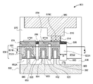
図7Aの左側を参照すると、エッチングされたSAGE壁キャップを有さない集積回路構造700は、フィン704をその上またはその上方に有する基板702を含む。フィン704の下部はシャロートレンチ分離構造706によって囲まれ、フィン704の上部はシャロートレンチ分離構造706の上方に突出する。ゲートスタック708は、それぞれ、1または複数のフィン704の上方、例えば、フィン704の対のそれぞれの上方にある。それぞれのゲートスタック708は、高kゲート誘電体などのゲート誘電体と、露出した上面を有するメタルゲート電極とを含んでよい。SAGE壁710は、ゲートスタック708の側面上かつこれらの間にある。それぞれのSAGE壁710は、低k誘電体壁712上に高k誘電体キャップ層714を有する。高k誘電体キャップ層714は、最上面715および最下面713を有する。ローカル導電性インターコネクト716は、隣接するゲートスタック708のメタルゲート電極の露出した上面を電気的に結合し、介在するSAGE壁(中間部710)の上方に延伸する。ローカル導電性インターコネクト716は、最上面719および最下面717を有する。ローカル導電性インターコネクト716の最下面717は、SAGE壁710の高k誘電体キャップ層714の最上面715の下方にある。
Referring to the left side of FIG. 7A, an
図7Aの右側を参照すると、部分的にエッチングされたSAGE壁キャップを有する集積回路構造720は、フィン704をその上またはその上方に有する基板702を含む。フィン704の下部はシャロートレンチ分離構造706によって囲まれ、フィン704の上部はシャロートレンチ分離構造706の上方に突出する。ゲートスタック708は、それぞれ、1または複数のフィン704の上方、例えば、フィン704の対のそれぞれの上方にある。それぞれのゲートスタック708は、高kゲート誘電体などのゲート誘電体と、露出した上面を有するメタルゲート電極とを含んでよい。SAGE壁722は、ゲートスタック708の側面上かつこれらの間にある。それぞれのSAGE壁722は、低k誘電体壁712上に高k誘電体キャップ層724を有する。高k誘電体キャップ層724は、最上面725を有する。
Referring to the right side of FIG. 7A, an
図7Aの右側を再び参照すると、本開示の実施形態によれば、集積回路構造720は、第1半導体フィン(左側のフィン704の対の1つ)上方に第1ゲート電極(左側の708)を含む。第2ゲート電極(右側の708)は、第2半導体フィン(右側のフィン704の対の1つ)の上方にある。ゲートエンドキャップ分離構造(中間部722)は、第1ゲート電極(左側の708)と第2ゲート電極(右側の708)との間にある。ゲートエンドキャップ分離構造722は、低k誘電体壁712上に高k誘電体キャップ層724を有する。ローカルインターコネクト726は、第1ゲート電極(左側の708)上、高k誘電体キャップ層(中間部724)上、かつ第2ゲート電極(右側の708)上にある。ローカルインターコネクト726は、高k誘電体キャップ層(中間部724)の最上面725の上方に最下面727を有する。
Referring again to the right side of FIG. 7A, according to embodiments of the present disclosure, an
一実施形態において、第1ゲート電極(左側の708)および第2ゲート電極(右側の708)は、それぞれ、ゲートエンドキャップ分離構造(中間部722)の高k誘電体キャップ層(中間部724)の最上面725と同一平面の最上面を有する。一実施形態において、ローカルインターコネクト726は、第1ゲート電極(左側の708)および第2ゲート電極(右側の708)を電気的に接続する。一実施形態において、ゲートエンドキャップ分離構造(中間部722)は、例えば、図9Cに関連して後述するように、低k誘電体壁712内の中心に鉛直シームを含む。
In one embodiment, the first gate electrode (708 on the left) and the second gate electrode (708 on the right) are each a high-k dielectric cap layer (middle portion 724) of the gate end cap isolation structure (middle portion 722). has a top surface coplanar with the
第2例において、図7Bは、本開示の実施形態に係るエッチングされたSAGE壁キャップを有さない集積回路構造(左側)および完全にエッチングされたSAGE壁キャップを有する集積回路構造(右側)のチャネル領域の断面図を示す。 In a second example, FIG. 7B shows an integrated circuit structure without etched SAGE wall caps (left) and with fully etched SAGE wall caps (right) according to embodiments of the present disclosure. FIG. 4 shows a cross-sectional view of a channel region;
図7Bの左側を参照すると、エッチングされたSAGE壁キャップを有さない集積回路構造700は、図7Aに関連して上述されたとおりである。図7Bの右側を参照すると、完全にエッチング/除去されたSAGE壁キャップを有する集積回路構造730は、フィン704をその上またはその上方に有する基板702を含む。フィン704の下部はシャロートレンチ分離構造706によって囲まれ、フィン704の上部はシャロートレンチ分離構造706の上方に突出する。ゲートスタック708は、それぞれ、1または複数のフィン704の上方、例えば、フィン704の対のそれぞれの上方にある。それぞれのゲートスタック708は、高kゲート誘電体などのゲート誘電体と、露出した上面を有するメタルゲート電極とを含んでよい。SAGE壁732は、ゲートスタック708の側面上かつこれらの間にある。それぞれのSAGE壁732は、低k誘電体壁734のみを含む。ローカル導電性インターコネクト736は、隣接するゲートスタック708のメタルゲート電極の露出した上面を電気的に結合し、介在するSAGE壁(中間部732)の上方に延伸する。一実施形態において、ローカル導電性インターコネクトの最下面は、図示されるように、ローカル導電性インターコネクト736の全体でプレーナ型である。
Referring to the left side of FIG. 7B, the
第3例において、図7Cは、本開示の実施形態に係るエッチングされたSAGE壁キャップを有さない集積回路構造(左側)、および部分的にエッチングされたSAGE壁キャップおよび完全にエッチングされたSAGE壁キャップの組み合わせを有する集積回路構造(右側)のチャネル領域の断面図を示す。 In a third example, FIG. 7C shows an integrated circuit structure without etched SAGE wall caps (left), and partially etched SAGE wall caps and fully etched SAGE according to embodiments of the present disclosure. FIG. 4 shows a cross-sectional view of a channel region of an integrated circuit structure (right side) with a wall cap combination.
図7Cの左側を参照すると、エッチングされたSAGE壁キャップを有さない集積回路構造700は、図7Aに関連して上述されたとおりである。図7Cの右側を参照すると、部分的にエッチングされたSAGE壁キャップおよび完全にエッチングされたSAGE壁キャップの両方を有する集積回路構造740は、フィン704をその上またはその上方に有する基板702を含む。フィン704の下部はシャロートレンチ分離構造706によって囲まれ、フィン704の上部はシャロートレンチ分離構造706の上方に突出する。ゲートスタック708は、それぞれ、1または複数のフィン704の上方、例えば、フィン704の対のそれぞれの上方にある。それぞれのゲートスタック708は、高kゲート誘電体などのゲート誘電体と、露出した上面を有するメタルゲート電極とを含んでよい。SAGE壁742Aは、ゲートスタック708の側面上にあり、SAGE壁742Bは、ゲートスタック708の間にある。それぞれのSAGE壁742Aは、低k誘電体壁上に高k誘電体キャップ層744を有する。高k誘電体キャップ層744は、最上面745および最下面743を有する。SAGE壁742Bは、低k誘電体壁746のみを有する。ローカル導電性インターコネクト748は、隣接するゲートスタック708のメタルゲート電極の露出した上面を電気的に結合し、介在するSAGE壁742Bの上方に延伸する。ローカル導電性インターコネクト748は、最下面742および最上面749を有する。ローカル導電性インターコネクト748の最下面742は、高k誘電体キャップ層744の最下面743と同一平面である。ローカル導電性インターコネクト748の最上面749は、SAGE壁742Aの高k誘電体キャップ層744の最上面745の上方にある。一実施形態において、ローカル導電性インターコネクト748の最下面742は、図示されるように、ローカル導電性インターコネクト748の全体でプレーナ型である。
Referring to the left side of FIG. 7C, the
図7Dは、本開示の実施形態に係るエッチングされたSAGE壁キャップを有さない集積回路構造(左側)および部分的にエッチングされたSAGE壁キャップを有する集積回路構造(右側)のソースまたはドレイン領域を通る断面図を示す。 FIG. 7D shows source or drain regions of integrated circuit structures without etched SAGE wall caps (left) and with partially etched SAGE wall caps (right) according to embodiments of the present disclosure. shows a cross-sectional view through the .
図7Dの左側を参照すると、エッチングされたSAGE壁キャップを有さない集積回路構造750は、フィン704をその上またはその上方に有する基板702を含む。フィン704の下部はシャロートレンチ分離構造706によって囲まれ、フィン704の上部はシャロートレンチ分離構造706の上方に突出する。導電性トレンチコンタクト756は、1または複数のフィン704のそれぞれの上方、例えば、フィン704の対のそれぞれの上方にあるエピタキシャルソースまたはドレイン構造752/754の上方にある。エピタキシャルソースまたはドレイン構造752および754は、反対の導電性を有してよい。SAGE壁710は、導電性トレンチコンタクト756の側面上かつこれらの間にある。それぞれのSAGE壁710は、低k誘電体壁712上に高k誘電体キャップ層714を有する。ローカル導電性インターコネクト758は、隣接する導電性トレンチコンタクト756の露出した上面を電気的に結合し、介在するSAGE壁(中間部710)の上方に延伸する。ローカル導電性インターコネクト716は、SAGE壁710の高k誘電体キャップ層714の最上面の下方に最下面を有する。
Referring to the left side of FIG. 7D, an
図7Dの右側を参照すると、部分的にエッチングされたSAGE壁キャップを有する集積回路構造760は、フィン704をその上またはその上方に有する基板702を含む。フィン704の下部はシャロートレンチ分離構造706によって囲まれ、フィン704の上部はシャロートレンチ分離構造706の上方に突出する。導電性トレンチコンタクト756(誘電体757に含まれてよい)は、1または複数のフィン704のそれぞれの上方、例えば、フィン704の対のそれぞれの上方にあるエピタキシャルソースまたはドレイン構造752/754の上方にある。エピタキシャルソースまたはドレイン構造752および754は、反対の導電性を有してよい。SAGE壁722は、導電性トレンチコンタクト756の側面上かつこれらの間にある。それぞれのSAGE壁722は、低k誘電体壁712上に高k誘電体キャップ層724を有する。高k誘電体キャップ層724は、最上面725を有する。ローカル導電性インターコネクト762は、隣接する導電性トレンチコンタクト756の露出した上面を電気的に結合し、介在するSAGE壁(中間部722)の上方に延伸する。ローカル導電性インターコネクト762は、最下面761および最上面763を有する。ローカル導電性インターコネクト762の最下面761は、SAGE壁722の高k誘電体キャップ層724の最上面725の上方にある。一実施形態において、ローカル導電性インターコネクト762の最下面761は、図示されるように、ローカル導電性インターコネクト762の全体でプレーナ型である。
Referring to the right side of FIG. 7D, integrated
図7Dの右側を再び参照すると、本開示の実施形態によれば、集積回路構造760は、第1半導体フィン(左側のフィンの対のフィン704の1つ)の上方の第1エピタキシャル構造752の上方に、第1トレンチコンタクト(左側の756)を含む。第2トレンチコンタクト(右側の756)は、第2半導体フィン(右側のフィンの対のフィン704の1つ)の上方の第2エピタキシャル構造754の上方にある。ゲートエンドキャップ分離構造(中間部722)は、第1トレンチコンタクト(左側の756)と第2トレンチコンタクト(右側の756)との間にある。ゲートエンドキャップ分離構造(中間部722)は、低k誘電体壁712上に高k誘電体キャップ層724を有する。ローカルインターコネクト756は、第1トレンチコンタクト(左側の756)上、高k誘電体キャップ層724上、かつ第2トレンチコンタクト(右側の756)上にある。ローカルインターコネクト762は、高k誘電体キャップ層724の最上面725の上方に最下面761を有する。
Referring again to the right side of FIG. 7D, according to an embodiment of the present disclosure, integrated
一実施形態において、第1トレンチコンタクト(左側の756)および第2トレンチコンタクト(右側の756)は、それぞれ、ゲートエンドキャップ分離構造(中間部722)の高k誘電体キャップ層724の最上面725と同一平面の最上面を有する。一実施形態において、ローカルインターコネクト762は、第1トレンチコンタクト(左側の756)および第2トレンチコンタクト(右側の756)を電気的に接続する。一実施形態において、ゲートエンドキャップ分離構造(中間部722)は、例えば、図9Cに関連して後述するように、低k誘電体壁712内の中心に鉛直シームを含む。
In one embodiment, the first trench contact (756 on the left) and the second trench contact (756 on the right) are each the
別の態様では、SAGE壁は、異なるデバイスについては、幅、位置、および機能が変化してよい。例示的な実装において、システムオンチップ(SoC)プロセス技術は、典型的には、標準的なロジック(例えば、低電圧、薄い酸化物)およびI/O(例えば、高電圧、厚い酸化物)トランジスタのサポートを必要とする。標準的なロジックと高電圧(HVI/O)デバイスとの間の区別は、マルチ酸化物プロセスシーケンスによって達成されてよく、ここで、ロジックトランジスタは、薄い高性能酸化物を受け、I/Oデバイスは、より高い電圧に耐え得る厚い酸化物を受ける。プロセス技術のスケーリングに伴い、ロジックデバイスは、寸法において積極的にスケーリングし、デュアル酸化物の形成に伴う製造上の課題を生み出す。本開示の1または複数の実施形態によれば、高電圧エンドキャッププロセスは、ウルトラスケーリングFinFETトランジスタアーキテクチャと組み合わせられ、SAGE構造の(全てではない場合には)少なくともいくつかがフィンエンドキャップなしで製造されるマルチ自己整合エンドキャッププロセスを提供する。 Alternatively, the SAGE walls may vary in width, position, and function for different devices. In exemplary implementations, system-on-chip (SoC) process technologies typically use standard logic (e.g., low voltage, thin oxide) and I/O (e.g., high voltage, thick oxide) transistors. need the support of The distinction between standard logic and high voltage (HVI/O) devices may be achieved by a multi-oxide process sequence, where logic transistors receive a thin high performance oxide and I/O devices receive thicker oxides that can withstand higher voltages. As process technology scales, logic devices scale aggressively in dimensions creating manufacturing challenges with dual oxide formation. According to one or more embodiments of the present disclosure, the high voltage endcap process is combined with an ultra-scaling FinFET transistor architecture such that at least some, if not all, of the SAGE structures are fabricated without fin endcaps. provides a multi-self aligned end capping process.
文脈を提供すべく、テクノロジーノードがより小さくスケーリングするのに伴い、狭いエンドキャップのロジックデバイスにおいて、高電圧トランジスタ製造で必要とされ得る無欠陥デュアル酸化物プロセスに適応する幾何学的空間の欠如が増加している。現在のアプローチは、単一のロジック酸化物プロセスに適応するために、単一のスケーリングされないエンドキャップスペースに依存している。しかしながら、エンドキャップスペースは両方の酸化物(ゲート誘電体)に適応するには不十分なことがあるので、そのようなプロセスは、デュアル酸化物高電圧SoC技術をサポートする、大きくスケーリングされた形状に適合しないことがある。 To provide context, as technology nodes scale smaller and smaller, there is a lack of geometric space in narrow end-cap logic devices to accommodate defect-free dual-oxide processes that may be required in high-voltage transistor fabrication. It has increased. Current approaches rely on a single unscaled end cap space to accommodate a single logic oxide process. However, the endcap space may be insufficient to accommodate both oxides (gate dielectrics), so such a process may be used in large scale geometries to support dual oxide high voltage SoC technology. may not be suitable for
本開示の実施形態によれば、高電圧酸化物およびロジック酸化物の両方で高電圧ゲートを充填する要件によって課されるスケーリングの制限が対処される。特に、ロジックの寸法が減少すると、高電圧(HV)デバイスにおけるエンドキャップスペースは、両方の酸化物を充填するには不十分な狭さになる。実施形態において、ロジックトランジスタと高電圧トランジスタとの間の異なるエンドキャップスペースは、それぞれ、SAGEアーキテクチャで製造される。ロジックトランジスタのエンドキャップは、自己整合エンドキャップアーキテクチャを使用することによってウルトラスケーリングされ、高電圧トランジスタは、より厚いゲート誘電体に適応するより広いエンドキャップを有する。一方または両方のタイプのエンドキャップが、本明細書で説明される実施形態によれば、フィンエンドキャップなしで製造可能である。 Embodiments of the present disclosure address scaling limitations imposed by the requirement to fill high voltage gates with both high voltage oxide and logic oxide. In particular, as logic dimensions decrease, the end cap space in high voltage (HV) devices becomes insufficiently narrow to fill both oxides. In an embodiment, different end cap spaces between the logic transistors and the high voltage transistors are each fabricated with a SAGE architecture. Logic transistor endcaps are ultrascaled by using a self-aligned endcap architecture, and high voltage transistors have wider endcaps to accommodate thicker gate dielectrics. One or both types of end caps can be manufactured without fin end caps according to embodiments described herein.
本明細書で説明される1または複数の実施形態は、ウルトラスケーリングロジックエンドキャップのための多方向-単方向エンドキャッププロセスフローに関し、またはこのように称されることがある。文脈を提供すべく、典型的なSAGEフローにおいて、単一のエンドキャップスペーサが成膜されて、フィンをSAGE壁から分離する自己整合エンドキャップを形成する。本明細書で説明される実施形態は、ロジックとHVゲートとの間で異なる犠牲スペーサ厚さの形成を含んでよい。その後、自己整合エンドキャップ壁が形成される。異なるスペーサ幅は、高電圧エリアにおいてより厚くなるように選択され、標準厚さは、ロジックエリアで使用される。異なるスペーサ幅は、ロジックエリアにおける密度を犠牲にすることなく、高電圧酸化物が成功裏に成膜することを可能にしてよい。実施形態において、異なるスペーサの厚さは、意図されるHV酸化物の厚さに従う。 One or more embodiments described herein relate to, or may be referred to as, a multidirectional-unidirectional endcap process flow for ultrascaling logic endcap. To provide context, in a typical SAGE flow, a single endcap spacer is deposited to form a self-aligned endcap that separates the fin from the SAGE wall. Embodiments described herein may include forming different sacrificial spacer thicknesses between logic and HV gates. Self-aligned end cap walls are then formed. Different spacer widths are chosen to be thicker in the high voltage areas and standard thickness is used in the logic areas. Different spacer widths may allow high voltage oxide to be successfully deposited without sacrificing density in the logic area. In embodiments, the different spacer thicknesses follow the intended HV oxide thickness.
完成したデバイスの例として、図8Aは、本開示の実施形態に係るマルチ自己整合ゲートエンドキャップ分離構造アーキテクチャを有する非プレーナ型半導体デバイスの断面図を示す。図8Bは、本開示の実施形態に係る図8Aの構造のa‐a'軸に沿った平面図を示す。 As an example of a completed device, FIG. 8A shows a cross-sectional view of a non-planar semiconductor device with multiple self-aligned gate end cap isolation structure architecture according to embodiments of the present disclosure. FIG. 8B shows a plan view along the aa′ axis of the structure of FIG. 8A according to an embodiment of the present disclosure.
図8Aを参照すると、半導体構造800は、基板802から、トレンチ分離層806内に形成された非プレーナ型活性領域(例えば、それぞれが突出したフィン部分804およびサブフィン領域805を含むフィン構造)を含む。実施形態において、フィン構造は、タイトピッチ格子構造などの格子構造を形成する複数のフィンラインである。そのような一実施形態において、タイトピッチは、従来のリソグラフィによっては直接実現可能ではない。例えば、従来のリソグラフィに基づくパターンがまず形成されてよいが、当技術分野において知られているように、スペーサマスクパターニングを使用してピッチが2分割されてよい。またさらに、元のピッチは、2回目のスペーサマスクパターニングによって4分割され得る。したがって、格子状フィンパターンは、一定のピッチで離隔され一定の幅を有するラインを有してよい。パターンは、ピッチ2分割もしくはピッチ4分割によって、または、他のピッチ分割のアプローチによって製造され得る。図示される個々のフィン804のそれぞれは、対応する個々のフィンを表してよく、または、特定の位置の複数のフィンを表してよい。
Referring to FIG. 8A, a
ゲート構造808は、非プレーナ型活性領域の突出部分804の上方かつトレンチ分離層806の部分の上方にある。示されるように、ゲート構造808は、ゲート電極850およびゲート誘電体層852を含む。一実施形態において、示されないが、ゲート構造808は、誘電体キャップ層を含んでもよい。
A
ゲート構造808は、狭い自己整合ゲートエンドキャップ(SAGE)分離構造または壁820、821Aまたは821Bによって分離される。SAGE壁820は、それぞれ幅を有する。実施形態において、SAGE壁821Aは、SAGE壁820のそれぞれの幅より大きい幅を有し、SAGE壁821Bは、SAGE壁820のそれぞれの幅より小さい幅を有する。異なる幅のSAGE壁は、本明細書で例示的な実施形態において説明されるように、異なるデバイスタイプに関連付けられてよい。SAGE壁の幅の変化は再構成可能であることが理解されるべきである。また、他の実施形態において、幅は全て同じである。SAGE壁820、821Aまたは821Bのそれぞれは、その上に形成されるローカルインターコネクト854または誘電体プラグ899の1または複数を含んでよい。実施形態において、SAGE壁820、821Aまたは821Bのそれぞれは、図8Aに図示されるように、トレンチ分離層806の最上面897の下方に窪んでいる。
本開示の実施形態によれば、SAGE壁821Aは、切断されたフィンの位置に形成される。特定の実施形態において、SAGE壁821Aは、図示されるように、フィンの切断部分869の上方に形成される。実施形態において、SAGE壁820、821Aおよび821Bは、フィン切断プロセスの後で製造される。
According to embodiments of the present disclosure,
例示的な実施形態において、半導体構造800は、基板802上方にあり、トレンチ分離層806の最上面897を通って突出する第1の複数の半導体フィン(領域870Aのフィンまたは複数のフィン804)と、第1の複数の半導体フィンの上方にある第1ゲート構造(領域870Aのゲート構造808)とを含む。第2の複数の半導体フィン(領域870Bのフィンまたは複数のフィン804)は、基板802の上方にあり、トレンチ分離層806の最上面897を通って突出し、第2ゲート構造(領域870Bのゲート構造808)は、第2の複数の半導体フィンの上方にある。ゲートエンドキャップ分離構造(SAGE壁820の左手)は、第1ゲート構造と第2ゲート構造との間にあり、これらと接触している。(領域870Aから)ゲートエンドキャップ分離構造に最も近い第1の複数の半導体フィンの半導体フィンは、(領域870Bから)ゲートエンドキャップ分離構造に最も近い第2の複数の半導体フィンの半導体フィンよりも、ゲートエンドキャップ分離構造からより離隔している。
In an exemplary embodiment,
実施形態において、領域870AはI/O領域であり、領域870Bはロジック領域である。図示されるように、そのような一実施形態において、第2ロジック領域870Cはロジック領域870Bに隣接し、ローカルインターコネクト854によってロジック領域870Bと電気的に接続されている。別の領域870Dは、追加のロジックまたはI/O領域が配置され得る位置であってよい。本明細書で説明される実施形態は、SAGE壁から異なる間隔(例えば、SAGE壁821Bおよび領域870Aの左手820からより広い間隔)を含んでよい、または、異なる幅のSAGE壁(例えば、より狭い821B対820対より広い821A)、もしくはSAGE壁からの異なる間隔および異なる幅のSAGE壁の両方を含んでよい。実施形態において、I/O領域は、SAGE壁の間にロジック領域より大きい間隔を有する。実施形態において、より広いSAGE壁は、隣接するI/O領域の間よりも、隣接するロジック領域の間にある。
In an embodiment,
ゲートコンタクト814およびその上に位置するゲートコンタクトビア816は、上に位置する金属インターコネクト860と共にこの透視図からも見られ、これら全ては層間絶縁膜スタックまたは層870にある。図8Aの透視図からも見られるように、一実施形態において、ゲートコンタクト814は非プレーナ型活性領域の上方にある。これも図8Aに示されるように、突出したフィン部分804とサブフィン領域805との間のドーピングプロファイルに境界880が存在するが、他の実施形態は、これらの領域の間のドーピングプロファイルにそのような境界を含まない。
図8Bを参照すると、ゲート構造808が、突出したフィン部分804の上方にあり、自己整合ゲートエンドキャップ分離構造820によって分離されるように示されている。実施形態において、ゲート構造808は、タイトピッチ格子構造などの格子構造を形成する複数の平行なゲートラインのうち1つのラインを形成する。そのような一実施形態において、タイトピッチは、従来のリソグラフィによっては直接実現可能ではない。例えば、従来のリソグラフィに基づくパターンがまず形成されてよいが、当技術分野において知られているように、スペーサマスクパターニングを使用してピッチが2分割されてよい。またさらに、元のピッチは、2回目のスペーサマスクパターニングによって4分割され得る。したがって、格子状ゲートパターンは、一定のピッチで離隔され一定の幅を有するラインを有してよい。パターンは、ピッチ2分割もしくはピッチ4分割によって、または、他のピッチ分割のアプローチによって製造され得る。
Referring to FIG. 8B,
図8Bを再び参照すると、突出したフィン部分804のソースおよびドレイン領域804Aおよび804Bがこの透視図に示されるが、これらの領域はトレンチコンタクト構造とオーバーラップしていることが理解されるべきである。一実施形態において、ソースおよびドレイン領域804Aおよび804Bは、突出したフィン部分804の原材のドーピングされた部分である。別の実施形態において、突出したフィン部分804の材料は除去され、例えばエピタキシャル成長によって、別の半導体材料に置換される。いずれの場合でも、ソースおよびドレイン領域804Aおよび804Bは、トレンチ分離層806の高さより下方に、すなわちサブフィン領域805内に延伸し得る。
Referring again to FIG. 8B, the source and
実施形態において、半導体構造800は、限定されないが、FinFETまたはトライゲートデバイスなどの非プレーナ型デバイスを含む。そのような実施形態において、対応する半導体チャネル領域は、3次元物体からなるか、または3次元物体に形成される。そのような一実施形態において、ゲート構造808は、3次元物体の少なくとも上面および側壁対を囲む。
In embodiments,
基板802は、製造プロセスに耐え得る、かつ電荷が移動し得る半導体材料からなるものであってよい。実施形態において、基板802は、活性領域804を形成すべく、限定されないが、リン、ヒ素、ホウ素、またはこれらの組み合わせなどの電荷キャリアでドーピングされた結晶シリコン、シリコン/ゲルマニウム、またはゲルマニウム層からなるバルク基板である。一実施形態において、バルク基板802のシリコン原子の濃度は、97%より大きい。別の実施形態において、バルク基板802は、別個の結晶基板上に成長するエピタキシャル層、例えば、ホウ素をドーピングされたバルクシリコン単結晶基板上に成長したシリコンエピタキシャル層からなる。あるいは、バルク基板802は、III‐V族材料からなるものであってよい。実施形態において、バルク基板802は、これに限定されないが、窒化ガリウム、リン化ガリウム、ヒ化ガリウム、リン化インジウム、アンチモン化インジウム、ヒ化ガリウムインジウム、ヒ化アルミニウムガリウム、リン化インジウムガリウム、またはこれらの組み合わせなどのIII‐V族材料からなる。一実施形態において、バルク基板802はIII‐V族材料からなり、電荷キャリアドーパント不純物原子は、これに限定されないが、炭素、ケイ素、ゲルマニウム、酸素、硫黄、セレンまたはテルルなどである。
トレンチ分離層806は、最終的には、下にあるバルク基板から恒久的なゲート構造の部分を電気的に分離するか、またはこれらの分離に寄与する、またはフィンの活性領域を分離するなど、下にあるバルク基板内に形成された活性領域を分離する好適な材料からなるものであってよい。例えば、一実施形態において、トレンチ分離層806は、限定されないが、二酸化シリコン、酸窒化シリコン、窒化シリコン、または炭素ドープ窒化シリコンなどの誘電体材料からなる。
The
自己整合ゲートエンドキャップ分離構造820、821Aおよび821Bは、最終的には恒久的なゲート構造の部分を互いから電気的に分離するか、またはこれらの分離に寄与する好適な材料または複数の材料からなるものであってよい。例示的な材料または材料の組み合わせは、二酸化シリコン、酸窒化シリコン、窒化シリコン、または炭素ドープ窒化シリコンなどの単一の材料構造を含む。他の例示的な材料または材料の組み合わせは、下部の二酸化シリコン、酸窒化シリコン、窒化シリコン、または炭素ドープ窒化シリコンと、酸化ハフニウムなどの高誘電体定数材料の上部とを有する多層スタックを含む。追加の例は、図9A-9Cに関連して後述される。
The self-aligned gate end
ゲート構造808は、ゲート誘電体層852およびゲート電極層850を含むゲート電極スタックからなるものであってよい。実施形態において、ゲート電極スタックのゲート電極はメタルゲートからなり、ゲート誘電体層は高k材料を含む。
例示的な実施形態において、領域870Aのゲート構造808は、第1の複数の半導体フィンにコンフォーマルであり、ゲートエンドキャップ分離構造の第1側面(左手820)の側方に隣接し、かつこれと接触している第1ゲート誘電体852を含む。領域870Bの第2ゲートスタックは、第2の複数の半導体フィンにコンフォーマルであり、ゲートエンドキャップ分離構造の第1側面と反対側のゲートエンドキャップ分離構造の第2側面の側方に隣接し、かつこれと接触している第2ゲート誘電体852を含む。一実施形態において、第1ゲート誘電体は、図8Aに図示されるように、第2ゲート誘電体より厚い。一実施形態において、第1ゲート誘電体は、第2ゲート誘電体(例えば、層852のみ)より多くの誘電体層(例えば、層852Aおよび852B)を有する。実施形態において、領域870Aのゲート誘電体はI/Oゲート誘電体であり、領域870Bのゲート誘電体はロジックゲート誘電体である。
In the exemplary embodiment,
実施形態において、領域870Bのゲート誘電体は、酸化ハフニウム、酸窒化ハフニウム、ケイ酸ハフニウム、酸化ランタン、酸化ジルコニウム、ケイ酸ジルコニウム、酸化タンタル、チタン酸バリウムストロンチウム、チタン酸バリウム、チタン酸ストロンチウム、酸化イットリウム、酸化アルミニウム、酸化タンタルスカンジウム鉛、亜鉛ニオブ酸鉛またはこれらの組み合わせなどの材料からなるが、これに限定されない。さらに、ゲート誘電体層の一部は、基板802のいくつかの上層から形成された自然酸化物の層を含んでよい。実施形態において、ゲート誘電体層は、上部高k部分と、半導体材料の酸化物からなる下部とからなる。一実施形態において、ゲート誘電体層は、酸化ハフニウムの上部と、二酸化シリコンまたは酸窒化シリコンの下部とからなる。実施形態において、上部高k部分は、基板の表面に実質的に平行な下部と、基板の上面に実質的に垂直な2つの側壁部分とを含む「U」字形構造からなる。実施形態において、領域870Aのゲート誘電体は、高k材料の層に加えて非ネイティブ酸化シリコンの層を含む。非ネイティブ酸化シリコンの層は、CVDプロセスを使用して形成されてよく、高k材料の層の下方または上方に形成されてよい。例示的な実施形態において、非ネイティブ酸化シリコンの層(例えば、層852A)は、高k材料の層(例えば、層852B)の下方に形成される。
In embodiments, the gate dielectric in
一実施形態において、ゲート電極は、限定されないが、金属窒化物、金属炭化物、金属ケイ化物、金属アルミニウム化物、ハフニウム、ジルコニウム、チタン、タンタル、アルミニウム、ルテニウム、パラジウム、プラチナ、コバルト、ニッケル、または導電性金属酸化物などの金属層からなる。具体的な実施形態において、ゲート電極は、金属の仕事関数設定層の上方に形成された非仕事関数設定充填材料からなる。いくつかの実装において、ゲート電極は、基板の表面に実質的に平行な下部と、基板の上面に実質的に垂直な2つの側壁部分とを含む「U」字形構造からなるものであってよい。別の実装において、ゲート電極を形成する金属層のうちの少なくとも1つは、基板の上面に対して実質的に平行であり、基板の上面に対して実質的に垂直な側壁部分を含まない単に平坦な層であり得る。本開示のさらなる実装において、ゲート電極は、U字形構造およびプレーナ型の、非U字形構造の組み合わせからなるものであってよい。例えば、ゲート電極は、1または複数のプレーナ型の非U字形層の上に形成される1または複数のU字形金属層からなるものであってよい。 In one embodiment, the gate electrode comprises, but is not limited to, metal nitrides, metal carbides, metal silicides, metal aluminides, hafnium, zirconium, titanium, tantalum, aluminum, ruthenium, palladium, platinum, cobalt, nickel, or conductive It consists of a metal layer, such as a reactive metal oxide. In a specific embodiment, the gate electrode consists of a non-workfunction setting fill material formed over a metal workfunction setting layer. In some implementations, the gate electrode may consist of a "U"-shaped structure including a bottom portion substantially parallel to the surface of the substrate and two sidewall portions substantially perpendicular to the top surface of the substrate. . In another implementation, at least one of the metal layers forming the gate electrode is substantially parallel to the top surface of the substrate and does not include sidewall portions that are substantially perpendicular to the top surface of the substrate. It can be a flat layer. In further implementations of the present disclosure, the gate electrode may consist of a combination of U-shaped structures and planar, non-U-shaped structures. For example, the gate electrode may consist of one or more U-shaped metal layers formed over one or more planar non-U-shaped layers.
ゲート電極スタックと関連したスペーサは、最終的には、自己整合コンタクトなどの隣接する導電性コンタクトから恒久的なゲート構造を電気的に分離するか、またはこの分離に寄与する好適な材料からなるものであってよい。例えば、一実施形態において、スペーサは、限定されないが、二酸化シリコン、酸窒化シリコン、窒化シリコン、または炭素ドープ窒化シリコンなどの誘電体材料からなる。 The spacers associated with the gate electrode stack are of a suitable material that ultimately electrically isolates or contributes to this isolation of the permanent gate structure from adjacent conductive contacts, such as self-aligned contacts. can be For example, in one embodiment, the spacer is made of a dielectric material such as, but not limited to, silicon dioxide, silicon oxynitride, silicon nitride, or carbon-doped silicon nitride.
ローカルインターコネクト854、ゲートコンタクト814、上に位置するゲートコンタクトビア816、および上に位置する金属インターコネクト860は、導電性材料からなるものであってよい。実施形態において、コンタクトまたはビアの1または複数は、金属種からなる。金属種は、タングステン、ニッケル、またはコバルトなどの純金属であってよく、または、金属間合金または金属-半導体合金(例えばシリサイド材料など)などの合金であってよい。一般的な例は、銅とこれを囲むILD材料との間にバリア層(TaまたはTaN層など)を含んでも含まなくてもよい銅構造の使用である。本明細書で使用されるように、金属という用語は、合金、スタック、および複数の金属の他の組み合わせを含む。例えば、金属インターコネクト線は、バリア層、異なる金属または合金のスタック等を含んでよい。
実施形態において(示されないが)、構造800を提供することは、既存のゲートパターンと実質的に完全に整合するコンタクトパターンの形成を含むが、非常にタイトな位置合わせ余裕度を伴うリソグラフィ工程の使用を取り除く。そのような一実施形態において、このアプローチにより、コンタクト開口を生成するために、(例えば従来実装されていたドライまたはプラズマエッチングに対して)本来的に選択性の高いウェットエッチングを使用することが可能となる。実施形態において、コンタクトパターンは、コンタクトプラグのリソグラフィ工程と組み合わせて、既存のゲートパターンを利用することにより形成される。そのような一実施形態において、本アプローチは、従来のアプローチに使用されるような、コンタクトパターンを生成するための別のクリティカルなリソグラフィ工程の必要性の除去を可能にする。実施形態において、トレンチコンタクトグリッドは、別個にパターニングされるのではなく、むしろポリ(ゲート)ラインの間に形成される。例えば、そのような一実施形態において、トレンチコンタクトグリッドは、ゲート格子パターニング後に、ゲート格子切断に先立って形成される。
In an embodiment (not shown), providing
さらに、ゲート構造808は、リプレースメントゲートプロセスによって製造されてよい。そのようなスキームでは、ポリシリコンまたは窒化シリコンピラー材料などのダミーゲート材料は除去され、恒久的なゲート電極材料に置換されてよい。そのような一実施形態において、恒久的なゲート誘電体層は、前のプロセスから持ち越されるのではなく、このプロセスにおいても形成される。実施形態において、ダミーゲートはドライまたはウェットエッチングプロセスによって除去される。一実施形態において、ダミーゲートは、多結晶シリコンまたはアモルファスシリコンからなり、SF6の使用を含むドライエッチングプロセスによって除去される。別の実施形態において、ダミーゲートは、多結晶シリコンまたはアモルファスシリコンからなり、NH4OH水溶液または水酸化テトラメチルアンモニウムの使用を含むウェットエッチングプロセスによって除去される。一実施形態において、ダミーゲートは窒化シリコンからなり、リン酸水溶液を含むウェットエッチングによって除去される。
Additionally,
実施形態において、本明細書で説明される1または複数のアプローチは、構造800に到達すべく、ダミーおよびリプレースメントコンタクトプロセスと組み合わせて、ダミーおよびリプレースメントゲートプロセスを実質的に意図している。そのような一実施形態において、リプレースメントコンタクトプロセスは、リプレースメントゲートプロセスの後で実行され、恒久的なゲートスタックの少なくとも一部の高温アニールを可能にする。例えば、そのような具体的実施形態では、恒久的なゲート構造の少なくとも一部のアニールは、例えば、ゲート誘電体層が形成された後で、摂氏約600度より高温で実行される。アニールは、恒久的なコンタクトの形成に先立って実行される。
In embodiments, one or more of the approaches described herein substantially contemplate dummy and replacement gate processes in combination with dummy and replacement contact processes to arrive at
図8Aを再び参照すると、実施形態において、半導体デバイスは、活性領域の上方に形成されたゲート電極の部分に接触するコンタクト構造を有する。一般的に、ゲートの活性部分の上方、かつトレンチコンタクトビアと同一の層に、ゲートコンタクト構造(ビアなど)を形成するのに先立って(例えば、それに加えて)、本開示の1または複数の実施形態は、ゲート整合トレンチコンタクトプロセスをまず使用することを含む。そのようなプロセスは、半導体構造の製造、例えば、集積回路の製造のためのトレンチコンタクト構造を形成するために実装されてよい。実施形態において、トレンチコンタクトパターンは、既存のゲートパターンに整合するように形成される。一方、従来のアプローチは、典型的には、選択性コンタクトエッチングと組み合わせた、既存のゲートパターンに対するリソグラフィコンタクトパターンの厳しい位置合わせを伴った追加のリソグラフィプロセスを含む。例えば、従来のプロセスは、コンタクトフィーチャの別個のパターニングと共に、ポリ(ゲート)グリッドのパターニングを含み得る。 Referring again to FIG. 8A, in an embodiment, the semiconductor device has a contact structure contacting a portion of the gate electrode formed over the active area. Generally, prior to (e.g., in addition to) forming a gate contact structure (such as a via) above the active portion of the gate and on the same layer as the trench contact via, one or more of the disclosed Embodiments include first using a gate aligned trench contact process. Such processes may be implemented in semiconductor structure fabrication, for example, to form trench contact structures for integrated circuit fabrication. In embodiments, the trench contact pattern is formed to match an existing gate pattern. Conventional approaches, on the other hand, typically involve additional lithographic processes with stringent alignment of the lithographic contact pattern to the existing gate pattern in combination with selective contact etching. For example, conventional processes may include patterning a poly (gate) grid along with separate patterning of contact features.
図8Aおよび8Bにおいて例示するように、幅の変化するSAGE壁が製造されてよいことが理解されるべきである。ゲートエンドキャップ分離構造の製造がゲートエンドキャップ分離構造内のシーム形成につながり得ることも理解されるべきである。誘電体層のスタックがSAGE壁を形成するために使用されてよいことも理解されるべきである。ゲートエンドキャップ分離構造は、隣接するフィンの間隔に応じて組成が異なってよいことも理解されるべきである。そのような態様を全て包含する例として、図9A-9Cは、本開示の実施形態に係るFinFETまたはトライゲートデバイスの別の自己整合ゲートエンドキャッププロセス製造スキームにおける重要なプロセス工程の断面図を示す。 It should be understood that SAGE walls of varying widths may be manufactured as illustrated in FIGS. 8A and 8B. It should also be appreciated that fabrication of the gate endcap isolation structure can lead to seam formation within the gate endcap isolation structure. It should also be understood that a stack of dielectric layers may be used to form the SAGE walls. It should also be appreciated that the gate endcap isolation structures may vary in composition depending on the spacing of adjacent fins. As an example encompassing all such aspects, FIGS. 9A-9C show cross-sectional views of key process steps in another self-aligned gate endcap process fabrication scheme for FinFET or Tri-Gate devices according to embodiments of the present disclosure. .
図9Aを参照すると、フィン900のグループは、間隔906を有する。フィン900のグループは、より大きい間隔904でフィン902に隣接している。犠牲スペーサ916は、複数の半導体フィン900および902のそれぞれの上部の側壁に隣接して形成されている。
Referring to FIG. 9A, groups of
図9Bを参照すると、複数のゲートエンドキャップ分離構造926および950が、犠牲スペーサ916の間に形成されている。本説明の目的のために、図示されるSAGE壁の少なくともいくつかは、フィン切断プロセスの後で製造される。実施形態において、図示されるように、間隔906の間に形成される複数のゲートエンドキャップ分離構造926のそれぞれは、下部誘電体部分928と、下部誘電体部分928上の誘電体キャップ930とを含む。実施形態において、複数のゲートエンドキャップ分離構造926は、成膜し、次に、窒化シリコン層などの第1誘電体材料に凹部を形成することによって形成され、下部誘電体部分928を提供する。成膜プロセスは、一実施形態において、下部誘電体部分928内にシーム932を提供するコンフォーマルプロセスであってよい。従って、実施形態において、複数のゲートエンドキャップ分離構造926のそれぞれは、ゲートエンドキャップ分離構造926内の中心に鉛直シーム932を含む。金属酸化物材料(例えば、酸化ハフニウム)などの誘電体キャップ材料は、次に、下部誘電体部分928上方の窪んだ領域に形成される。誘電体キャップ材料は、誘電体キャップ930を形成するために平坦化されてよく、または、誘電体キャップ930を直接提供するために、上方へ成長してよい。
Referring to FIG. 9B, a plurality of gate end
図9Bを再び参照すると、実施形態において、ゲートエンドキャップ分離構造926は、間隔906を有する半導体フィンの間にあり、ゲートエンドキャップ分離構造950は、間隔904を有する半導体フィンの間にある。ゲートエンドキャップ分離構造926は、ゲートエンドキャップ分離構造950の対応する幅より狭い幅を有する。一実施形態において、ゲートエンドキャップ分離構造926は、ゲートエンドキャップ分離構造950の全組成と異なる全組成を有する。そのような一実施形態において、ゲートエンドキャップ分離構造950は、下部誘電体部分952の下部上かつその側壁内に、酸化シリコン層などの第3の誘電体層956をさらに含む。さらに、誘電体キャップ954が、第3の誘電体層956上にある。実施形態において、図9Bに図示されるように、下部誘電体部分952の側壁は、第3の誘電体層956の最上面とほぼ同一平面にある最上面を有し、誘電体キャップ954は、実質的にプレーナ型の最下面を有する。別の実施形態において、下部誘電体部分952の側壁は、第3の誘電体層956の最上面の下方に最上面を有し、誘電体キャップ954は、側壁の位置の上方でさらに下方へ延伸する。さらに別の実施形態において、下部誘電体部分952の側壁は、第3の誘電体層956の最上面の上方に最上面を有し、誘電体キャップ954は、第3の誘電体層956の上方でさらに下方へ延伸する。
Referring again to FIG. 9B, in an embodiment, gate endcap
実施形態において、第3の誘電体層956の成膜プロセスは、一実施形態において、第3の誘電体層956内に鉛直シーム958を提供するコンフォーマルプロセスである。しかしながら、別の実施形態において、シーム958は、より広い構造では形成されないが、より狭い構造で形成される(例えば、上述したシーム932)。下部誘電体部分928および952は、窒化シリコンなどの同一の材料からなるものであってよく、互いに同時に形成されてよいことが理解されるべきである。誘電体キャップ930および954は、酸化ハフニウムなどの同一の材料からなるものであってよく、互いに同時に形成されてよいことも理解されるべきである。構造926からは省略されているが、構造950の第3の誘電体層956は、構造全体にわたってコンフォーマル成膜によって形成されてよいが、下部誘電体部分928は、間隔904を完全には充填しない第1成膜プロセスにおいて間隔906を実質的に充填するので、構造926から除外されている。
In an embodiment, the deposition process of the third
図9Cを参照すると、犠牲スペーサ916が除去されている。実施形態において、犠牲スペーサ916は、ウェットエッチングまたはドライエッチングプロセスによって除去される。実施形態において、フィン上方のスタック層のパターニングも除去され、フィン900'および902'を提供する。
Referring to FIG. 9C, the
図9Cを再び参照すると、実施形態において、ゲートエンドキャップ分離構造926または950は、トレンチ分離層の最上面の下方にある、対応する凹部にある。実施形態において、ゲートエンドキャップ分離構造926または950は、下部誘電体部分と、下部誘電体部分上の誘電体キャップとを含む。実施形態において、ゲートエンドキャップ分離構造926または950は、第2ゲートエンドキャップ分離構造内の中心に鉛直シームを含む。実施形態において、第1ゲートエンドキャップ分離構造926は、例えば、追加の充填誘電体材料を含むことによって、第2ゲートエンドキャップ分離構造950の全組成とは全組成が異なる。
Referring again to FIG. 9C, in an embodiment, the gate
ゲートエンドキャップ分離構造926または950が下部誘電体部分と下部誘電体部分上の誘電体キャップとを含む実施形態において、ゲートエンドキャップ分離構造926または950は、まず成膜し、次に、SiN層、SiCN層、SiOCN層、SiOC層、またはSiC層などの第1誘電体材料に凹部を形成することによって形成されてよく、これにより下部誘電体部分を提供する。一実施形態において、第1誘電体材料は窒化シリコン層である。金属酸化物材料(例えば、酸化ハフニウム、酸化ハフニウム-アルミニウム、または酸化アルミニウム)などの誘電体キャップ材料は、次に、下部誘電体部分上方の窪んだ領域に形成される。一実施形態において、金属酸化物材料は酸化ハフニウムである。別の実施形態において、誘電体キャップ材料は低k誘電体材料である。誘電体キャップ材料は、誘電体キャップを形成するために平坦化されてよく、または、誘電体キャップを直接提供するために、上方へ成長してよい。
In embodiments where the gate endcap
上述された1または複数の実施形態は、FinFETデバイスのSAGE壁のためのキャップ低減または除去に関する。他の実施形態は、2つの類似しない半導体材料(例えば、SiおよびSiGe、またはSiGeおよびGe)の交互の層からなるフィンにそのようなアプローチを適用することを含み得ることが理解されるべきである。類似しない半導体材料の対の1つは、次に、ゲート領域において除去可能であり、これによりゲートオールアラウンドデバイスにナノワイヤ/ナノリボンチャネルを提供する。実施形態において、ゲートオールアラウンドデバイスへのアプローチは、ゲート領域におけるナノワイヤ/リボンのリリース工程を追加することにより、FinFETへの上述のアプローチと類似する。 One or more embodiments described above relate to cap reduction or removal for SAGE walls in FinFET devices. It should be appreciated that other embodiments may include applying such an approach to fins composed of alternating layers of two dissimilar semiconductor materials (eg, Si and SiGe, or SiGe and Ge). be. One of the pair of dissimilar semiconductor materials can then be removed in the gate region, thereby providing a nanowire/nanoribbon channel for the gate-all-around device. In embodiments, the approach to gate-all-around devices is similar to that described above for FinFETs by adding a nanowire/ribbon release step in the gate region.
実施形態において、本明細書全体で使用されるように、層間誘電体(ILD)材料は、誘電体もしくは絶縁材料の層からなる、またはこれを含む。好適な誘電体材料の例は、限定されないが、シリコン酸化物(例えば二酸化シリコン(SiO2))、ドーピングシリコン酸化物、フッ化シリコン酸化物、炭素ドーピングシリコン酸化物、当技術分野において知られている様々な低k誘電体材料、およびこれらの組み合わせを含む。ILD材料は、例えば化学気相成長(CVD)、物理気相成長(PVD)などの従来技術によって、または他の成膜方法によって形成され得る。 In embodiments, as used throughout this specification, an interlevel dielectric (ILD) material consists of or includes a layer of dielectric or insulating material. Examples of suitable dielectric materials include, but are not limited to, silicon oxides (e.g., silicon dioxide ( SiO2 )), doped silicon oxides, fluorinated silicon oxides, carbon-doped silicon oxides, known in the art. various low-k dielectric materials, and combinations thereof. ILD materials may be formed by conventional techniques such as chemical vapor deposition (CVD), physical vapor deposition (PVD), or by other deposition methods.
実施形態において、本明細書全体にわたっても使用されるように、金属線またはインターコネクト線材料(およびビア材料)は、1または複数の金属または他の導電性構造からなる。一般的な例は、銅とこれを囲むILD材料との間にバリア層を含んでも含まなくてもよい銅線および構造の使用である。本明細書で使用されるように、金属という用語は、合金、スタック、および複数の金属の他の組み合わせを含む。例えば、金属インターコネクト線は、バリア層(例えば、Ta、TaN、Ti、またはTiNのうちの1または複数を含む層)、異なる金属または合金のスタック等を含み得る。従って、インターコネクト線は、単一材料層であり得るか、または、導電性ライナ層および充填層を含む複数の層から形成され得る。電気めっき、化学気相成長または物理気相成長など、任意の好適な成膜プロセスが、インターコネクト線を形成するために使用され得る。実施形態において、インターコネクト線は、これらに限定されないが、Cu、Al、Ti、Zr、Hf、V、Ru、Co、Ni、Pd、Pt、W、Mo、Ag、Au、またはそれらの合金などの導電性材料からなる。インターコネクト線は、場合により、当技術分野において、トレース、ワイヤ、ライン、金属、または単にインターコネクトと称されることもある。 In embodiments, and as also used throughout this specification, a metal line or interconnect line material (and via material) consists of one or more metals or other conductive structures. A common example is the use of copper lines and structures that may or may not include a barrier layer between the copper and the surrounding ILD material. As used herein, the term metal includes alloys, stacks, and other combinations of metals. For example, metal interconnect lines may include barrier layers (eg, layers including one or more of Ta, TaN, Ti, or TiN), stacks of different metals or alloys, and the like. Thus, the interconnect line can be a single layer of material or can be formed from multiple layers including a conductive liner layer and a filler layer. Any suitable deposition process may be used to form the interconnect lines, such as electroplating, chemical vapor deposition or physical vapor deposition. In embodiments, the interconnect lines are made of metal such as, but not limited to, Cu, Al, Ti, Zr, Hf, V, Ru, Co, Ni, Pd, Pt, W, Mo, Ag, Au, or alloys thereof. Made of conductive material. Interconnect lines are sometimes referred to in the art as traces, wires, lines, metals, or simply interconnects.
実施形態において、これも本明細書の全体にわたって使用されるように、ハードマスク材料、キャップ層、またはプラグは、層間誘電体材料とは異なる誘電体材料からなる。一実施形態において、異なる成長またはエッチング選択性を互いにまた下層の誘電体および金属層に提供するよう、異なる領域に異なるハードマスク、キャップまたはプラグ材料が使用されてよい。いくつかの実施形態において、ハードマスク層、キャップまたはプラグ層は、シリコン窒化物(例えば窒化シリコン)の層もしくはシリコン酸化物の層、もしくはその両方、またはそれらの組み合わせを含む。他の好適な材料は、炭素ベース材料を含み得る。具体的な実装に応じて、当技術分野において知られている他のハードマスク、キャップまたはプラグ層が使用されてよい。ハードマスク、キャップまたはプラグ層は、CVD、PVD、または他の成膜方法によって形成されてよい。 In embodiments, as also used throughout this specification, the hard mask material, cap layer, or plug consists of a dielectric material different from the interlevel dielectric material. In one embodiment, different hardmask, cap or plug materials may be used in different regions to provide different growth or etch selectivities to each other and to underlying dielectric and metal layers. In some embodiments, the hardmask layer, cap or plug layer comprises a layer of silicon nitride (eg, silicon nitride) or a layer of silicon oxide, or both, or a combination thereof. Other suitable materials may include carbon-based materials. Other hardmask, cap or plug layers known in the art may be used depending on the specific implementation. A hardmask, cap or plug layer may be formed by CVD, PVD, or other deposition methods.
実施形態において、これも本明細書の全体にわたって使用されるように、リソグラフィ工程は、193nm浸漬リソ(i193)、EUVおよび/またはEBDWリソグラフィ等を使用して実行される。ポジ型またはネガ型のレジストが使用されてよい。一実施形態において、リソグラフィマスクは、トポグラフィマスキング部分、反射防止コーティング(ARC)層、およびフォトレジスト層からなる3層マスクである。特定のそのような実施形態において、トポグラフィマスキング部分は、炭素ハードマスク(CHM)層であり、反射防止コーティング層はシリコンARC層である。 In embodiments, as also used throughout this specification, lithographic steps are performed using 193 nm immersion litho (i193), EUV and/or EBDW lithography, and the like. A positive or negative resist may be used. In one embodiment, the lithographic mask is a three-layer mask consisting of a topographic masking portion, an antireflective coating (ARC) layer, and a photoresist layer. In certain such embodiments, the topographic masking portion is a carbon hardmask (CHM) layer and the antireflective coating layer is a silicon ARC layer.
本明細書に開示される実施形態は、多種多様な異なるタイプの集積回路および/またはマイクロエレクトロニクスデバイスを製造するために使用されてよい。そのような集積回路の例は、限定されないが、プロセッサ、チップセットコンポーネント、グラフィックプロセッサ、デジタル信号プロセッサ、マイクロコントローラ等を含む。他の実施形態において、半導体メモリが製造されてよい。さらに、集積回路または他のマイクロエレクトロニクスデバイスは、当技術分野において知られている多種多様な電子デバイスにおいて使用され得る。例えば、コンピュータシステム(例えば、デスクトップ、ラップトップ、サーバ)、携帯電話、パーソナル電子機器等において使用され得る。集積回路は、バスおよびシステム内の他のコンポーネントと結合されてよい。例えば、プロセッサは、1または複数のバスによって、メモリ、チップセット等と結合されてよい。プロセッサ、メモリ、およびチップセットのそれぞれは、潜在的に、本明細書に開示されるアプローチを使用して製造されてよい。 The embodiments disclosed herein may be used to manufacture a wide variety of different types of integrated circuits and/or microelectronic devices. Examples of such integrated circuits include, but are not limited to, processors, chipset components, graphics processors, digital signal processors, microcontrollers, and the like. In other embodiments, semiconductor memory may be manufactured. Additionally, integrated circuits or other microelectronic devices may be used in a wide variety of electronic devices known in the art. For example, it can be used in computer systems (eg, desktops, laptops, servers), mobile phones, personal electronics, and the like. The integrated circuit may be combined with buses and other components in the system. For example, a processor may be coupled to memory, chipsets, etc. by one or more buses. Each of the processors, memories, and chipsets may potentially be manufactured using the approaches disclosed herein.
図10は、本開示の実施形態の一実装に係るコンピューティングデバイス1000を示す。コンピューティングデバイス1000は、ボード1002を収容する。ボード1002は、限定されないが、プロセッサ1004および少なくとも1つの通信チップ1006を含む多数のコンポーネントを含み得る。プロセッサ1004は、ボード1002と物理的かつ電気的に結合されている。いくつかの実装において、少なくとも1つの通信チップ1006も、ボード1002と物理的かつ電気的に結合されている。さらなる実装において、通信チップ1006は、プロセッサ1004の一部である。
FIG. 10 illustrates a computing device 1000 according to one implementation of embodiments of the disclosure. Computing device 1000 houses board 1002 . Board 1002 may include numerous components including, but not limited to,
その適用に応じて、コンピューティングデバイス1000は、ボード1002と物理的かつ電気的に結合されていてもいなくてもよい他のコンポーネントを含み得る。これらの他のコンポーネントは、限定されないが、揮発性メモリ(例えば、DRAM)、不揮発性メモリ(例えば、ROM)、フラッシュメモリ、グラフィックプロセッサ、デジタル信号プロセッサ、暗号プロセッサ、チップセット、アンテナ、ディスプレイ、タッチスクリーンディスプレイ、タッチスクリーンコントローラ、バッテリ、オーディオコーデック、ビデオコーデック、パワーアンプ、全地球測位システム(GPS)デバイス、コンパス、加速度計、ジャイロスコープ、スピーカ、カメラ、および(例えば、ハードディスクドライブ、コンパクトディスク(CD)、デジタル多用途ディスク(DVD)等の)大容量記憶装置を含む。 Depending on its application, computing device 1000 may include other components that may or may not be physically and electrically coupled to board 1002 . These other components include, but are not limited to, volatile memory (eg, DRAM), non-volatile memory (eg, ROM), flash memory, graphics processors, digital signal processors, cryptographic processors, chipsets, antennas, displays, touch screen displays, touch screen controllers, batteries, audio codecs, video codecs, power amplifiers, global positioning system (GPS) devices, compasses, accelerometers, gyroscopes, speakers, cameras, and (e.g., hard disk drives, compact discs (CD ), Digital Versatile Disc (DVD), etc.).
通信チップ1006は、コンピューティングデバイス1000との間でのデータの転送のための無線通信を可能にする。「無線」という用語およびその派生語は、非固体媒体を介した変調電磁放射の使用を介してデータを通信し得る回路、デバイス、システム、方法、技術、通信チャネル等を説明するために使用されてよい。この用語は、関連デバイスが有線を一切含まないことを示唆するものではないが、いくつかの実施形態においては含まないことがある。通信チップ1006は、Wi-Fi(登録商標)(IEEE802.11ファミリ)、WiMAX(登録商標)(IEEE802.16ファミリ)、IEEE802.20、ロングタームエボリューション(LTE)、Ev-DO、HSPA+、HSDPA+、HSUPA+、EDGE、GSM(登録商標)、GPRS、CDMA、TDMA、DECT、Bluetooth(登録商標)、それらの派生物、ならびに3G、4G、5Gおよびそれ以降のものとして指定される任意の他の無線プロトコルを含むがこれらに限定されない多数の無線規格またはプロトコルのいずれかを実装してよい。コンピューティングデバイス1000は、複数の通信チップ1006を含み得る。例えば、第1通信チップ1006は、Wi-FiおよびBluetooth(登録商標)などの短距離無線通信の専用であってよく、第2通信チップ1006は、例えばGPS、EDGE、GPRS、CDMA、WiMAX、LTE、およびEv-DOなどの長距離無線通信の専用であってよい。
コンピューティングデバイス1000のプロセッサ1004は、プロセッサ1004内にパッケージされた集積回路ダイを含む。プロセッサ1004の集積回路ダイは、本開示の実施形態の実装に従って構築された自己整合ゲートエンドキャップ(SAGE)構造などの1または複数の構造を含み得る。「プロセッサ」という用語は、レジスタおよび/またはメモリからの電子データを処理して、当該電子データをレジスタおよび/またはメモリに格納され得る他の電子データに変換する任意のデバイスまたはデバイスの部分を指してよい。
通信チップ1006は、通信チップ1006内にパッケージされた集積回路ダイも含む。通信チップ1006の集積回路ダイは、本開示の実施形態の実装に従って構築された自己整合ゲートエンドキャップ(SAGE)構造などの1または複数の構造を含み得る。
さらなる実装において、コンピューティングデバイス1000内に収容される別のコンポーネントは、本開示の実施形態の実装に従って構築される自己整合ゲートエンドキャップ(SAGE)構造などの構造を1または複数含む集積回路ダイを含んでよい。 In further implementations, another component housed within computing device 1000 is an integrated circuit die that includes one or more structures such as self-aligned gate end cap (SAGE) structures constructed according to implementations of embodiments of the present disclosure. may contain.
様々な実装において、コンピューティングデバイス1000は、ラップトップ、ネットブック、ノートブック、ウルトラブック、スマートフォン、タブレット、パーソナルデジタルアシスタント(PDA)、ウルトラモバイルPC、携帯電話、デスクトップコンピュータ、サーバ、プリンタ、スキャナ、モニタ、セットトップボックス、エンターテイメントコントロールユニット、デジタルカメラ、携帯音楽プレーヤまたはデジタルビデオレコーダであってよい。さらなる実装において、コンピューティングデバイス1000は、データを処理する任意の他の電子デバイスであってよい。 In various implementations, the computing device 1000 can be a laptop, netbook, notebook, ultrabook, smartphone, tablet, personal digital assistant (PDA), ultra-mobile PC, cell phone, desktop computer, server, printer, scanner, It may be a monitor, set-top box, entertainment control unit, digital camera, portable music player or digital video recorder. In further implementations, computing device 1000 may be any other electronic device that processes data.
図11は、本開示の1または複数の実施形態を含むインターポーザ1100を示す。インターポーザ1100は、第1基板1102と第2基板1104とのブリッジになるために使用される介在基板である。第1基板1102は、例えば、集積回路ダイであってよい。第2基板1104は、例えば、メモリモジュール、コンピュータマザーボード、または別の集積回路ダイであってよい。一般に、インターポーザ1100の目的は、接続部をより広いピッチに広げること、または接続部を異なる接続部にリルートすることである。例えば、インターポーザ1100は、後で第2基板1104に結合され得るボールグリッドアレイ(BGA)1106に、集積回路ダイを結合してよい。いくつかの実施形態において、第1基板および第2基板1102/1104は、インターポーザ1100の反対側に取り付けられる。他の実施形態において、第1基板および第2基板1102/1104は、インターポーザ1100の同じ側に取り付けられる。そして、さらなる実施形態において、3またはそれより多くの基板が、インターポーザ1100によって相互接続される。
FIG. 11 shows an
インターポーザ1100は、エポキシ樹脂、ガラス繊維強化エポキシ樹脂、セラミック材料、またはポリイミドなどのポリマー材料で形成されてよい。さらなる実装において、インターポーザ1100は、シリコン、ゲルマニウム、並びに他のIII‐V族およびIV族材料などの、半導体基板に使用される上述された材料と同一の材料を含み得る、交互に重なる剛性または可撓性材料で形成され得る。
インターポーザ1100は、金属インターコネクト1108と、限定されないが、スルーシリコンビア(TSV)1112を含むビア1110とを含み得る。インターポーザ1100は、受動および能動デバイスの両方を含む埋め込みデバイス1114をさらに含んでよい。そのようなデバイスは、限定されないが、コンデンサ、デカップリングコンデンサ、抵抗器、インダクタ、ヒューズ、ダイオード、変圧器、センサ、および静電気放電(ESD)デバイスを含む。無線周波数(RF)デバイス、パワーアンプ、電力管理デバイス、アンテナ、アレイ、センサ、およびMEMSデバイスなどのより複雑なデバイスも、インターポーザ1100上に形成されてよい。本開示の実施形態によれば、本明細書で開示される装置またはプロセスは、インターポーザ1100の製造またはインターポーザ1100に含まれるコンポーネントの製造において使用されてよい。
従って、本開示の実施形態は、キャップが低減または除去された自己整合ゲートエンドキャップ(SAGE)アーキテクチャ、およびキャップが低減または除去された自己整合ゲートエンドキャップ(SAGE)アーキテクチャの製造方法を含む。 Accordingly, embodiments of the present disclosure include self-aligned gate endcap (SAGE) architectures with reduced or eliminated caps and methods of manufacturing self-aligned gate endcap (SAGE) architectures with reduced or eliminated caps.
本開示の実施形態の例示された実装の上述した説明は、要約で説明されるものを含み、網羅的であること、または開示された正確な形態に開示を限定することは意図されない。本開示の具体的な実装および例は、例示目的のために本明細書で説明されるが、当業者であれば理解するであろうように、様々な均等な変形が、本開示の範囲内で可能である。 The above description of example implementations of embodiments of the disclosure, including what is set forth in the Abstract, is not intended to be exhaustive or to limit the disclosure to the precise forms disclosed. Although specific implementations and examples of the disclosure are described herein for purposes of illustration, various equivalent modifications are within the scope of the disclosure, as will be appreciated by those skilled in the art. is possible.
これらの変形は、詳細に上述した説明に鑑みれば、開示に加えることができる。以下の特許請求の範囲において使用される用語は、本明細書および特許請求の範囲において開示される具体的な実装例に、本開示を限定するものと解釈されるべきではない。むしろ、本開示の範囲は、以下の特許請求の範囲によってのみ決定されるべきであり、特許請求の範囲は、特許請求の範囲の解釈の確立された原則に従って解釈されるべきである。 These variations can be added to the disclosure in light of the detailed above description. The terms used in the following claims should not be construed to limit the disclosure to the specific implementations disclosed in the specification and claims. Rather, the scope of the disclosure is to be determined solely by the following claims, which are to be construed in accordance with established doctrines of claim interpretation.
例示的実施形態1:集積回路構造は、第1半導体フィンの上方に第1ゲート電極を含む。第2ゲート電極は、第2半導体フィンの上方にある。ゲートエンドキャップ分離構造は、第1ゲート電極と第2ゲート電極との間にあり、ゲートエンドキャップ分離構造は、低k誘電体壁上に高k誘電体キャップ層を有する。ローカルインターコネクトは、第1ゲート電極上、高k誘電体キャップ層上、かつ第2ゲート電極上にあり、ローカルインターコネクトは、高k誘電体キャップ層の最上面の上方に最下面を有する。 Exemplary embodiment 1: An integrated circuit structure includes a first gate electrode over a first semiconductor fin. A second gate electrode overlies the second semiconductor fin. A gate endcap isolation structure is between the first gate electrode and the second gate electrode, the gate endcap isolation structure having a high k dielectric capping layer on the low k dielectric wall. A local interconnect overlies the first gate electrode, the high-k dielectric capping layer, and the second gate electrode, the local interconnect having a bottom surface above the top surface of the high-k dielectric capping layer.
例示的実施形態2:第1ゲート電極および第2ゲート電極は、それぞれ、ゲートエンドキャップ分離構造の高k誘電体キャップ層の最上面と同一平面の最上面を有する、例示的実施形態1に記載の集積回路構造。 Exemplary embodiment 2: As described in exemplary embodiment 1, wherein the first gate electrode and the second gate electrode each have a top surface coplanar with a top surface of the high-k dielectric cap layer of the gate endcap isolation structure. integrated circuit structure.
例示的実施形態3:ローカルインターコネクトは、第1ゲート電極および第2ゲート電極を電気的に接続する、例示的実施形態1または2に記載の集積回路構造。 Exemplary embodiment 3: The integrated circuit structure of exemplary embodiment 1 or 2, wherein the local interconnect electrically connects the first gate electrode and the second gate electrode.
例示的実施形態4:ゲートエンドキャップ分離構造は、低k誘電体壁内の中心に鉛直シームを含む、例示的実施形態1、2または3に記載の集積回路構造。 Exemplary Embodiment 4: The integrated circuit structure of Exemplary Embodiment 1, 2 or 3, wherein the gate endcap isolation structure comprises a vertical seam centrally within the low-k dielectric wall.
例示的実施形態5:集積回路構造は、第1半導体フィンの上方の第1エピタキシャル構造の上方に第1トレンチコンタクトを含む。第2トレンチコンタクトは、第2半導体フィンの上方の第2エピタキシャル構造の上方にある。ゲートエンドキャップ分離構造は、第1トレンチコンタクトと第2トレンチコンタクトとの間にあり、ゲートエンドキャップ分離構造は、低k誘電体壁上に高k誘電体キャップ層を有する。ローカルインターコネクトは、第1トレンチコンタクト上、高k誘電体キャップ層上、かつ第2トレンチコンタクト上にあり、ローカルインターコネクトは、高k誘電体キャップ層の最上面の上方に最下面を有する。 Exemplary embodiment 5: An integrated circuit structure includes a first trench contact over a first epitaxial structure over a first semiconductor fin. A second trench contact is over the second epitaxial structure over the second semiconductor fin. A gate endcap isolation structure is between the first trench contact and the second trench contact, the gate endcap isolation structure having a high k dielectric capping layer on the low k dielectric wall. A local interconnect is on the first trench contact, on the high-k dielectric capping layer, and on the second trench contact, the local interconnect having a bottom surface above the top surface of the high-k dielectric capping layer.
例示的実施形態6:第1トレンチコンタクトおよび第2トレンチコンタクトは、それぞれ、ゲートエンドキャップ分離構造の高k誘電体キャップ層の最上面と同一平面の最上面を有する、例示的実施形態5に記載の集積回路構造。 Exemplary embodiment 6: The method of exemplary embodiment 5 wherein the first trench contact and the second trench contact each have a top surface coplanar with a top surface of the high-k dielectric cap layer of the gate endcap isolation structure. integrated circuit structure.
例示的実施形態7:ローカルインターコネクトは、第1トレンチコンタクトおよび第2トレンチコンタクトを電気的に接続する、請例示的実施形態5または6に記載の集積回路構造。 Exemplary embodiment 7: The integrated circuit structure of exemplary embodiment 5 or 6, wherein the local interconnect electrically connects the first trench contact and the second trench contact.
例示的実施形態8:ゲートエンドキャップ分離構造は、低k誘電体壁内の中心に鉛直シームを含む、例示的実施形態5、6または7に記載の集積回路構造。 Exemplary Embodiment 8: The integrated circuit structure of Exemplary Embodiment 5, 6 or 7, wherein the gate endcap isolation structure comprises a vertical seam centrally within the low-k dielectric wall.
例示的実施形態9:コンピューティングデバイスは、ボードと、ボードに結合されたコンポーネントとを含む。コンポーネントは、集積回路構造を含む。集積回路構造は、第1半導体フィンの上方に第1ゲート電極を含む。第2ゲート電極は、第2半導体フィンの上方にある。ゲートエンドキャップ分離構造は、第1ゲート電極と第2ゲート電極との間にあり、ゲートエンドキャップ分離構造は、低k誘電体壁上に高k誘電体キャップ層を有する。ローカルインターコネクトは、第1ゲート電極上、高k誘電体キャップ層上、かつ第2ゲート電極上にあり、ローカルインターコネクトは、高k誘電体キャップ層の最上面の上方に最下面を有する。 Exemplary embodiment 9: A computing device includes a board and components coupled to the board. Components include integrated circuit structures. The integrated circuit structure includes a first gate electrode overlying the first semiconductor fin. A second gate electrode overlies the second semiconductor fin. A gate endcap isolation structure is between the first gate electrode and the second gate electrode, the gate endcap isolation structure having a high k dielectric capping layer on the low k dielectric wall. A local interconnect overlies the first gate electrode, the high-k dielectric capping layer, and the second gate electrode, the local interconnect having a bottom surface above the top surface of the high-k dielectric capping layer.
例示的実施形態10:ボードに結合されたメモリをさらに含む、例示的実施形態9に記載のコンピューティングデバイス。 Exemplary embodiment 10: The computing device of exemplary embodiment 9, further comprising memory coupled to the board.
例示的実施形態11:ボードに結合された通信チップをさらに含む、例示的実施形態9または10に記載のコンピューティングデバイス。 Exemplary embodiment 11: The computing device of exemplary embodiment 9 or 10, further comprising a communications chip coupled to the board.
例示的実施形態12:ボードに結合されたカメラをさらに含む、例示的実施形態9、10または11に記載のコンピューティングデバイス。 Exemplary embodiment 12: The computing device of exemplary embodiment 9, 10, or 11, further comprising a camera coupled to the board.
例示的実施形態13:コンポーネントはパッケージされた集積回路ダイである、例示的実施形態9、10、11または12に記載のコンピューティングデバイス。 Exemplary embodiment 13: The computing device of exemplary embodiment 9, 10, 11, or 12, wherein the component is a packaged integrated circuit die.
例示的実施形態14:コンピューティングデバイスは、携帯電話、ラップトップ、デスクトップコンピュータ、サーバ、およびセットトップボックスからなる群から選択される、例示的実施形態9、10、11、12または13に記載のコンピューティングデバイス。 Exemplary Embodiment 14: According to Exemplary Embodiment 9, 10, 11, 12, or 13, the computing device is selected from the group consisting of mobile phones, laptops, desktop computers, servers, and set-top boxes. computing device.
例示的実施形態15:コンピューティングデバイスは、ボードと、ボードに結合されたコンポーネントとを含む。コンポーネントは、集積回路構造を含む。集積回路構造は、第1半導体フィンの上方の第1エピタキシャル構造の上方に第1トレンチコンタクトを含む。第2トレンチコンタクトは、第2半導体フィンの上方の第2エピタキシャル構造の上方にある。ゲートエンドキャップ分離構造は、第1トレンチコンタクトと第2トレンチコンタクトとの間にあり、ゲートエンドキャップ分離構造は、低k誘電体壁上に高k誘電体キャップ層を有する。ローカルインターコネクトは、第1トレンチコンタクト上、高k誘電体キャップ層上、かつ第2トレンチコンタクト上にあり、ローカルインターコネクトは、高k誘電体キャップ層の最上面の上方に最下面を有する。 Exemplary embodiment 15: A computing device includes a board and components coupled to the board. Components include integrated circuit structures. The integrated circuit structure includes a first trench contact over the first epitaxial structure over the first semiconductor fin. A second trench contact is over the second epitaxial structure over the second semiconductor fin. A gate endcap isolation structure is between the first trench contact and the second trench contact, the gate endcap isolation structure having a high k dielectric capping layer on the low k dielectric wall. A local interconnect is on the first trench contact, on the high-k dielectric capping layer, and on the second trench contact, the local interconnect having a bottom surface above the top surface of the high-k dielectric capping layer.
例示的実施形態16:ボードに結合されたメモリをさらに含む、例示的実施形態15に記載のコンピューティングデバイス。 Exemplary embodiment 16: The computing device of exemplary embodiment 15, further comprising memory coupled to the board.
例示的実施形態17:ボードに結合された通信チップをさらに含む、例示的実施形態15または16に記載のコンピューティングデバイス。 Exemplary embodiment 17: The computing device of exemplary embodiment 15 or 16, further comprising a communications chip coupled to the board.
例示的実施形態18:ボードに結合されたカメラをさらに含む、例示的実施形態15、16または17に記載のコンピューティングデバイス。 Exemplary embodiment 18: The computing device of exemplary embodiment 15, 16, or 17, further comprising a camera coupled to the board.
例示的実施形態19:コンポーネントはパッケージされた集積回路ダイである、例示的実施形態15、16、17または18に記載のコンピューティングデバイス。 Exemplary embodiment 19: The computing device of exemplary embodiment 15, 16, 17, or 18, wherein the component is a packaged integrated circuit die.
例示的実施形態20:コンピューティングデバイスは、携帯電話、ラップトップ、デスクトップコンピュータ、サーバ、およびセットトップボックスからなる群から選択される、例示的実施形態15、16、17、18または19に記載のコンピューティングデバイス。
他の可能な態様
[項目1]
第1半導体フィン上方の第1ゲート電極と、
第2半導体フィン上方の第2ゲート電極と、
前記第1ゲート電極と前記第2ゲート電極との間のゲートエンドキャップ分離構造であって、低k誘電体壁上に高k誘電体キャップ層を有するゲートエンドキャップ分離構造と、
前記第1ゲート電極上、前記高k誘電体キャップ層上、かつ前記第2ゲート電極上のローカルインターコネクトであって、前記高k誘電体キャップ層の最上面の上方に最下面を有するローカルインターコネクトと
を備える集積回路構造。
[項目2]
第1ゲート電極および前記第2ゲート電極は、それぞれ、前記ゲートエンドキャップ分離構造の前記高k誘電体キャップ層の前記最上面と同一平面の最上面を有する、項目1に記載の集積回路構造。
[項目3]
前記ローカルインターコネクトは、前記第1ゲート電極および前記第2ゲート電極を電気的に接続する、項目1に記載の集積回路構造。
[項目4]
前記ゲートエンドキャップ分離構造は、前記低k誘電体壁内の中心に鉛直シームを有する、項目1に記載の集積回路構造。
[項目5]
第1半導体フィン上方の第1エピタキシャル構造上方の第1トレンチコンタクトと、
第2半導体フィン上方の第2エピタキシャル構造上方の第2トレンチコンタクトと、
前記第1トレンチコンタクトと前記第2トレンチコンタクトとの間のゲートエンドキャップ分離構造であって、低k誘電体壁上に高k誘電体キャップ層を有するゲートエンドキャップ分離構造と、
前記第1トレンチコンタクト上、前記高k誘電体キャップ層上、かつ前記第2トレンチコンタクト上のローカルインターコネクトであって、前記高k誘電体キャップ層の最上面の上方に最下面を有するローカルインターコネクトと
を備える集積回路構造。
[項目6]
前記第1トレンチコンタクトおよび前記第2トレンチコンタクトは、それぞれ、前記ゲートエンドキャップ分離構造の前記高k誘電体キャップ層の前記最上面と同一平面の最上面を有する、項目5に記載の集積回路構造。
[項目7]
前記ローカルインターコネクトは、前記第1トレンチコンタクトおよび前記第2トレンチコンタクトを電気的に接続する、項目5に記載の集積回路構造。
[項目8]
前記ゲートエンドキャップ分離構造は、前記低k誘電体壁内の中心に鉛直シームを有する、項目5に記載の集積回路構造。
[項目9]
ボードと、
前記ボードに結合されたコンポーネントであって、集積回路構造を含むコンポーネントと
を備えるコンピューティングデバイスであって、
前記集積回路構造は、
第1半導体フィン上方の第1ゲート電極と、
第2半導体フィン上方の第2ゲート電極と、
前記第1ゲート電極と前記第2ゲート電極との間のゲートエンドキャップ分離構造であって、低k誘電体壁上に高k誘電体キャップ層を有するゲートエンドキャップ分離構造と、
前記第1ゲート電極上、前記高k誘電体キャップ層上、かつ前記第2ゲート電極上のローカルインターコネクトであって、前記高k誘電体キャップ層の最上面の上方に最下面を有するローカルインターコネクトと
を有する、コンピューティングデバイス。
[項目10]
前記ボードに結合されたメモリをさらに備える項目9に記載のコンピューティングデバイス。
[項目11]
前記ボードに結合された通信チップをさらに備える項目9に記載のコンピューティングデバイス。
[項目12]
前記ボードに結合されたカメラをさらに備える項目9に記載のコンピューティングデバイス。
[項目13]
前記コンポーネントはパッケージされた集積回路ダイである、項目9に記載のコンピューティングデバイス。
[項目14]
前記コンピューティングデバイスは、携帯電話、ラップトップ、デスクトップコンピュータ、サーバ、およびセットトップボックスからなる群から選択される、項目9に記載のコンピューティングデバイス。
[項目15]
ボードと、
前記ボードに結合されたコンポーネントであって、集積回路構造を含むコンポーネントと
を備えるコンピューティングデバイスであって、
前記集積回路構造は、
第1半導体フィン上方の第1エピタキシャル構造上方の第1トレンチコンタクトと、
第2半導体フィン上方の第2エピタキシャル構造上方の第2トレンチコンタクトと、
前記第1トレンチコンタクトと前記第2トレンチコンタクトとの間のゲートエンドキャップ分離構造であって、低k誘電体壁上に高k誘電体キャップ層を有するゲートエンドキャップ分離構造と、
前記第1トレンチコンタクト上、前記高k誘電体キャップ層上、かつ前記第2トレンチコンタクト上のローカルインターコネクトであって、前記高k誘電体キャップ層の最上面の上方に最下面を有するローカルインターコネクトと
を有する、コンピューティングデバイス。
[項目16]
前記ボードに結合されたメモリをさらに備える項目15に記載のコンピューティングデバイス。
[項目17]
前記ボードに結合された通信チップをさらに備える項目15に記載のコンピューティングデバイス。
[項目18]
前記ボードに結合されたカメラをさらに備える項目15に記載のコンピューティングデバイス。
[項目19]
前記コンポーネントはパッケージされた集積回路ダイである、項目15に記載のコンピューティングデバイス。
[項目20]
前記コンピューティングデバイスは、携帯電話、ラップトップ、デスクトップコンピュータ、サーバ、およびセットトップボックスからなる群から選択される、項目15に記載のコンピューティングデバイス。
Exemplary embodiment 20: according to exemplary embodiment 15, 16, 17, 18 or 19, wherein the computing device is selected from the group consisting of a mobile phone, a laptop, a desktop computer, a server, and a set top box computing device.
Other possible modes [Item 1]
a first gate electrode above the first semiconductor fin;
a second gate electrode above the second semiconductor fin;
a gate end cap isolation structure between the first gate electrode and the second gate electrode, the gate end cap isolation structure having a high k dielectric cap layer on a low k dielectric wall;
a local interconnect over the first gate electrode, the high-k dielectric capping layer, and the second gate electrode, the local interconnect having a bottom surface above a top surface of the high-k dielectric capping layer; An integrated circuit structure comprising:
[Item 2]
2. The integrated circuit structure of item 1, wherein the first gate electrode and the second gate electrode each have a top surface coplanar with the top surface of the high-k dielectric capping layer of the gate endcap isolation structure.
[Item 3]
2. The integrated circuit structure of item 1, wherein the local interconnect electrically connects the first gate electrode and the second gate electrode.
[Item 4]
2. The integrated circuit structure of claim 1, wherein the gate endcap isolation structure has a vertical seam centered within the low-k dielectric wall.
[Item 5]
a first trench contact above the first epitaxial structure above the first semiconductor fin;
a second trench contact above the second epitaxial structure above the second semiconductor fin;
a gate end cap isolation structure between the first trench contact and the second trench contact, the gate end cap isolation structure having a high k dielectric cap layer on a low k dielectric wall;
a local interconnect over the first trench contact, the high-k dielectric capping layer, and the second trench contact, the local interconnect having a bottom surface above a top surface of the high-k dielectric capping layer; An integrated circuit structure comprising:
[Item 6]
6. The integrated circuit structure of item 5, wherein the first trench contact and the second trench contact each have a top surface coplanar with the top surface of the high-k dielectric cap layer of the gate endcap isolation structure. .
[Item 7]
6. The integrated circuit structure of item 5, wherein the local interconnect electrically connects the first trench contact and the second trench contact.
[Item 8]
6. The integrated circuit structure of item 5, wherein the gate endcap isolation structure has a vertical seam centrally within the low-k dielectric wall.
[Item 9]
a board;
a component coupled to the board, the component comprising an integrated circuit structure,
The integrated circuit structure comprises:
a first gate electrode above the first semiconductor fin;
a second gate electrode above the second semiconductor fin;
a gate end cap isolation structure between the first gate electrode and the second gate electrode, the gate end cap isolation structure having a high k dielectric cap layer on a low k dielectric wall;
a local interconnect over the first gate electrode, the high-k dielectric capping layer, and the second gate electrode, the local interconnect having a bottom surface above a top surface of the high-k dielectric capping layer; A computing device having a
[Item 10]
10. The computing device of item 9, further comprising a memory coupled to said board.
[Item 11]
10. A computing device according to item 9, further comprising a communication chip coupled to said board.
[Item 12]
10. The computing device of item 9, further comprising a camera coupled to said board.
[Item 13]
10. The computing device of item 9, wherein the component is a packaged integrated circuit die.
[Item 14]
10. The computing device of item 9, wherein the computing device is selected from the group consisting of mobile phones, laptops, desktop computers, servers, and set-top boxes.
[Item 15]
a board;
a component coupled to the board, the component comprising an integrated circuit structure, the computing device comprising:
The integrated circuit structure comprises:
a first trench contact above the first epitaxial structure above the first semiconductor fin;
a second trench contact above the second epitaxial structure above the second semiconductor fin;
a gate end cap isolation structure between the first trench contact and the second trench contact, the gate end cap isolation structure having a high k dielectric cap layer on a low k dielectric wall;
a local interconnect over the first trench contact, the high-k dielectric capping layer, and the second trench contact, the local interconnect having a bottom surface above a top surface of the high-k dielectric capping layer; A computing device having a
[Item 16]
16. A computing device as recited in item 15, further comprising a memory coupled to said board.
[Item 17]
16. A computing device according to item 15, further comprising a communication chip coupled to said board.
[Item 18]
16. A computing device according to item 15, further comprising a camera coupled to said board.
[Item 19]
16. A computing device according to item 15, wherein the component is a packaged integrated circuit die.
[Item 20]
16. The computing device of item 15, wherein the computing device is selected from the group consisting of mobile phones, laptops, desktop computers, servers, and set-top boxes.
Claims (20)
第2半導体フィン上方の第2ゲート電極と、
前記第1ゲート電極と前記第2ゲート電極との間のゲートエンドキャップ分離構造であって、低k誘電体壁上に高k誘電体キャップ層を有するゲートエンドキャップ分離構造と、
前記第1ゲート電極上、前記高k誘電体キャップ層上、かつ前記第2ゲート電極上のローカルインターコネクトであって、前記高k誘電体キャップ層の最上面の上方に最下面を有するローカルインターコネクトと
を備える集積回路構造。 a first gate electrode above the first semiconductor fin;
a second gate electrode above the second semiconductor fin;
a gate end cap isolation structure between the first gate electrode and the second gate electrode, the gate end cap isolation structure having a high k dielectric cap layer on a low k dielectric wall;
a local interconnect over the first gate electrode, the high-k dielectric capping layer, and the second gate electrode, the local interconnect having a bottom surface above a top surface of the high-k dielectric capping layer; An integrated circuit structure comprising:
第2半導体フィン上方の第2エピタキシャル構造上方の第2トレンチコンタクトと、
前記第1トレンチコンタクトと前記第2トレンチコンタクトとの間のゲートエンドキャップ分離構造であって、低k誘電体壁上に高k誘電体キャップ層を有するゲートエンドキャップ分離構造と、
前記第1トレンチコンタクト上、前記高k誘電体キャップ層上、かつ前記第2トレンチコンタクト上のローカルインターコネクトであって、前記高k誘電体キャップ層の最上面の上方に最下面を有するローカルインターコネクトと
を備える集積回路構造。 a first trench contact above the first epitaxial structure above the first semiconductor fin;
a second trench contact above the second epitaxial structure above the second semiconductor fin;
a gate end cap isolation structure between the first trench contact and the second trench contact, the gate end cap isolation structure having a high k dielectric cap layer on a low k dielectric wall;
a local interconnect over the first trench contact, the high-k dielectric capping layer, and the second trench contact, the local interconnect having a bottom surface above a top surface of the high-k dielectric capping layer; An integrated circuit structure comprising:
前記ボードに結合されたコンポーネントであって、集積回路構造を含むコンポーネントと
を備えるコンピューティングデバイスであって、
前記集積回路構造は、
第1半導体フィン上方の第1ゲート電極と、
第2半導体フィン上方の第2ゲート電極と、
前記第1ゲート電極と前記第2ゲート電極との間のゲートエンドキャップ分離構造であって、低k誘電体壁上に高k誘電体キャップ層を有するゲートエンドキャップ分離構造と、
前記第1ゲート電極上、前記高k誘電体キャップ層上、かつ前記第2ゲート電極上のローカルインターコネクトであって、前記高k誘電体キャップ層の最上面の上方に最下面を有するローカルインターコネクトと
を有する、コンピューティングデバイス。 a board;
a component coupled to the board, the component comprising an integrated circuit structure,
The integrated circuit structure comprises:
a first gate electrode above the first semiconductor fin;
a second gate electrode above the second semiconductor fin;
a gate end cap isolation structure between the first gate electrode and the second gate electrode, the gate end cap isolation structure having a high k dielectric cap layer on a low k dielectric wall;
a local interconnect over the first gate electrode, the high-k dielectric capping layer, and the second gate electrode, the local interconnect having a bottom surface above a top surface of the high-k dielectric capping layer; A computing device having a
前記ボードに結合されたコンポーネントであって、集積回路構造を含むコンポーネントと
を備えるコンピューティングデバイスであって、
前記集積回路構造は、
第1半導体フィン上方の第1エピタキシャル構造上方の第1トレンチコンタクトと、
第2半導体フィン上方の第2エピタキシャル構造上方の第2トレンチコンタクトと、
前記第1トレンチコンタクトと前記第2トレンチコンタクトとの間のゲートエンドキャップ分離構造であって、低k誘電体壁上に高k誘電体キャップ層を有するゲートエンドキャップ分離構造と、
前記第1トレンチコンタクト上、前記高k誘電体キャップ層上、かつ前記第2トレンチコンタクト上のローカルインターコネクトであって、前記高k誘電体キャップ層の最上面の上方に最下面を有するローカルインターコネクトと
を有する、コンピューティングデバイス。 a board;
a component coupled to the board, the component comprising an integrated circuit structure,
The integrated circuit structure comprises:
a first trench contact above the first epitaxial structure above the first semiconductor fin;
a second trench contact above the second epitaxial structure above the second semiconductor fin;
a gate end cap isolation structure between the first trench contact and the second trench contact, the gate end cap isolation structure having a high k dielectric cap layer on a low k dielectric wall;
a local interconnect over the first trench contact, the high-k dielectric capping layer, and the second trench contact, the local interconnect having a bottom surface above a top surface of the high-k dielectric capping layer; A computing device having a
Applications Claiming Priority (2)
| Application Number | Priority Date | Filing Date | Title |
|---|---|---|---|
| US17/211,751 US20220310818A1 (en) | 2021-03-24 | 2021-03-24 | Self-aligned gate endcap (sage) architectures with reduced cap |
| US17/211,751 | 2021-03-24 |
Publications (1)
| Publication Number | Publication Date |
|---|---|
| JP2022151587A true JP2022151587A (en) | 2022-10-07 |
Family
ID=83365082
Family Applications (1)
| Application Number | Title | Priority Date | Filing Date |
|---|---|---|---|
| JP2022004048A Pending JP2022151587A (en) | 2021-03-24 | 2022-01-14 | Self-aligned gate endcap (sage) architectures with reduced cap |
Country Status (2)
| Country | Link |
|---|---|
| US (1) | US20220310818A1 (en) |
| JP (1) | JP2022151587A (en) |
-
2021
- 2021-03-24 US US17/211,751 patent/US20220310818A1/en active Pending
-
2022
- 2022-01-14 JP JP2022004048A patent/JP2022151587A/en active Pending
Also Published As
| Publication number | Publication date |
|---|---|
| US20220310818A1 (en) | 2022-09-29 |
Similar Documents
| Publication | Publication Date | Title |
|---|---|---|
| US11276691B2 (en) | Gate-all-around integrated circuit structures having self-aligned source or drain undercut for varied widths | |
| US11855223B2 (en) | Self-aligned gate endcap (SAGE) architectures with gate-all-around devices | |
| US10950606B2 (en) | Dual fin endcap for self-aligned gate edge (SAGE) architectures | |
| US11715775B2 (en) | Self-aligned gate endcap (SAGE) architectures with gate-all-around devices having epitaxial source or drain structures | |
| US11329138B2 (en) | Self-aligned gate endcap (SAGE) architecture having endcap plugs | |
| US11605632B2 (en) | Unidirectional self-aligned gate endcap (SAGE) architectures with gate-orthogonal walls | |
| US20200066712A1 (en) | Metal resistor and self-aligned gate edge (sage) architecture having a metal resistor | |
| US11688792B2 (en) | Dual self-aligned gate endcap (SAGE) architectures | |
| US20240088143A1 (en) | Self-aligned gate endcap (sage) architectures without fin end gap | |
| US11749733B2 (en) | FIN shaping using templates and integrated circuit structures resulting therefrom | |
| US11563000B2 (en) | Gate endcap architectures having relatively short vertical stack | |
| EP3678189A1 (en) | Self-aligned gate endcap (sage) architectures with gate-all-around devices above insulator substrates | |
| JP2022151587A (en) | Self-aligned gate endcap (sage) architectures with reduced cap | |
| US20220093590A1 (en) | Selective growth self-aligned gate endcap (sage) architectures without fin end gap | |
| US20210351300A1 (en) | Self-aligned gate endcap (sage) architectures with vertical sidewalls |