JP2022106295A - Photoresist resolution capabilities by copper electroplating anisotropically - Google Patents
Photoresist resolution capabilities by copper electroplating anisotropically Download PDFInfo
- Publication number
- JP2022106295A JP2022106295A JP2022000874A JP2022000874A JP2022106295A JP 2022106295 A JP2022106295 A JP 2022106295A JP 2022000874 A JP2022000874 A JP 2022000874A JP 2022000874 A JP2022000874 A JP 2022000874A JP 2022106295 A JP2022106295 A JP 2022106295A
- Authority
- JP
- Japan
- Prior art keywords
- copper
- plating
- seed layer
- mol
- substrate
- Prior art date
- Legal status (The legal status is an assumption and is not a legal conclusion. Google has not performed a legal analysis and makes no representation as to the accuracy of the status listed.)
- Granted
Links
Images

Classifications
-
- C—CHEMISTRY; METALLURGY
- C25—ELECTROLYTIC OR ELECTROPHORETIC PROCESSES; APPARATUS THEREFOR
- C25D—PROCESSES FOR THE ELECTROLYTIC OR ELECTROPHORETIC PRODUCTION OF COATINGS; ELECTROFORMING; APPARATUS THEREFOR
- C25D5/00—Electroplating characterised by the process; Pretreatment or after-treatment of workpieces
- C25D5/60—Electroplating characterised by the structure or texture of the layers
- C25D5/615—Microstructure of the layers, e.g. mixed structure
- C25D5/617—Crystalline layers
-
- C—CHEMISTRY; METALLURGY
- C25—ELECTROLYTIC OR ELECTROPHORETIC PROCESSES; APPARATUS THEREFOR
- C25D—PROCESSES FOR THE ELECTROLYTIC OR ELECTROPHORETIC PRODUCTION OF COATINGS; ELECTROFORMING; APPARATUS THEREFOR
- C25D5/00—Electroplating characterised by the process; Pretreatment or after-treatment of workpieces
- C25D5/60—Electroplating characterised by the structure or texture of the layers
- C25D5/605—Surface topography of the layers, e.g. rough, dendritic or nodular layers
-
- C—CHEMISTRY; METALLURGY
- C25—ELECTROLYTIC OR ELECTROPHORETIC PROCESSES; APPARATUS THEREFOR
- C25D—PROCESSES FOR THE ELECTROLYTIC OR ELECTROPHORETIC PRODUCTION OF COATINGS; ELECTROFORMING; APPARATUS THEREFOR
- C25D3/00—Electroplating: Baths therefor
- C25D3/02—Electroplating: Baths therefor from solutions
- C25D3/38—Electroplating: Baths therefor from solutions of copper
-
- C—CHEMISTRY; METALLURGY
- C25—ELECTROLYTIC OR ELECTROPHORETIC PROCESSES; APPARATUS THEREFOR
- C25D—PROCESSES FOR THE ELECTROLYTIC OR ELECTROPHORETIC PRODUCTION OF COATINGS; ELECTROFORMING; APPARATUS THEREFOR
- C25D21/00—Processes for servicing or operating cells for electrolytic coating
- C25D21/12—Process control or regulation
- C25D21/14—Controlled addition of electrolyte components
-
- C—CHEMISTRY; METALLURGY
- C25—ELECTROLYTIC OR ELECTROPHORETIC PROCESSES; APPARATUS THEREFOR
- C25D—PROCESSES FOR THE ELECTROLYTIC OR ELECTROPHORETIC PRODUCTION OF COATINGS; ELECTROFORMING; APPARATUS THEREFOR
- C25D5/00—Electroplating characterised by the process; Pretreatment or after-treatment of workpieces
- C25D5/02—Electroplating of selected surface areas
- C25D5/022—Electroplating of selected surface areas using masking means
-
- C—CHEMISTRY; METALLURGY
- C25—ELECTROLYTIC OR ELECTROPHORETIC PROCESSES; APPARATUS THEREFOR
- C25D—PROCESSES FOR THE ELECTROLYTIC OR ELECTROPHORETIC PRODUCTION OF COATINGS; ELECTROFORMING; APPARATUS THEREFOR
- C25D7/00—Electroplating characterised by the article coated
-
- C—CHEMISTRY; METALLURGY
- C25—ELECTROLYTIC OR ELECTROPHORETIC PROCESSES; APPARATUS THEREFOR
- C25D—PROCESSES FOR THE ELECTROLYTIC OR ELECTROPHORETIC PRODUCTION OF COATINGS; ELECTROFORMING; APPARATUS THEREFOR
- C25D7/00—Electroplating characterised by the article coated
- C25D7/12—Semiconductors
- C25D7/123—Semiconductors first coated with a seed layer or a conductive layer
-
- G—PHYSICS
- G03—PHOTOGRAPHY; CINEMATOGRAPHY; ANALOGOUS TECHNIQUES USING WAVES OTHER THAN OPTICAL WAVES; ELECTROGRAPHY; HOLOGRAPHY
- G03F—PHOTOMECHANICAL PRODUCTION OF TEXTURED OR PATTERNED SURFACES, e.g. FOR PRINTING, FOR PROCESSING OF SEMICONDUCTOR DEVICES; MATERIALS THEREFOR; ORIGINALS THEREFOR; APPARATUS SPECIALLY ADAPTED THEREFOR
- G03F7/00—Photomechanical, e.g. photolithographic, production of textured or patterned surfaces, e.g. printing surfaces; Materials therefor, e.g. comprising photoresists; Apparatus specially adapted therefor
- G03F7/20—Exposure; Apparatus therefor
-
- H—ELECTRICITY
- H05—ELECTRIC TECHNIQUES NOT OTHERWISE PROVIDED FOR
- H05K—PRINTED CIRCUITS; CASINGS OR CONSTRUCTIONAL DETAILS OF ELECTRIC APPARATUS; MANUFACTURE OF ASSEMBLAGES OF ELECTRICAL COMPONENTS
- H05K3/00—Apparatus or processes for manufacturing printed circuits
- H05K3/10—Apparatus or processes for manufacturing printed circuits in which conductive material is applied to the insulating support in such a manner as to form the desired conductive pattern
- H05K3/107—Apparatus or processes for manufacturing printed circuits in which conductive material is applied to the insulating support in such a manner as to form the desired conductive pattern by filling grooves in the support with conductive material
-
- H—ELECTRICITY
- H05—ELECTRIC TECHNIQUES NOT OTHERWISE PROVIDED FOR
- H05K—PRINTED CIRCUITS; CASINGS OR CONSTRUCTIONAL DETAILS OF ELECTRIC APPARATUS; MANUFACTURE OF ASSEMBLAGES OF ELECTRICAL COMPONENTS
- H05K3/00—Apparatus or processes for manufacturing printed circuits
- H05K3/22—Secondary treatment of printed circuits
- H05K3/24—Reinforcing of the conductive pattern
- H05K3/241—Reinforcing of the conductive pattern characterised by the electroplating method; means therefor, e.g. baths or apparatus
-
- G—PHYSICS
- G03—PHOTOGRAPHY; CINEMATOGRAPHY; ANALOGOUS TECHNIQUES USING WAVES OTHER THAN OPTICAL WAVES; ELECTROGRAPHY; HOLOGRAPHY
- G03F—PHOTOMECHANICAL PRODUCTION OF TEXTURED OR PATTERNED SURFACES, e.g. FOR PRINTING, FOR PROCESSING OF SEMICONDUCTOR DEVICES; MATERIALS THEREFOR; ORIGINALS THEREFOR; APPARATUS SPECIALLY ADAPTED THEREFOR
- G03F7/00—Photomechanical, e.g. photolithographic, production of textured or patterned surfaces, e.g. printing surfaces; Materials therefor, e.g. comprising photoresists; Apparatus specially adapted therefor
- G03F7/26—Processing photosensitive materials; Apparatus therefor
- G03F7/40—Treatment after imagewise removal, e.g. baking
Landscapes
- Chemical & Material Sciences (AREA)
- Engineering & Computer Science (AREA)
- Chemical Kinetics & Catalysis (AREA)
- Electrochemistry (AREA)
- Materials Engineering (AREA)
- Metallurgy (AREA)
- Organic Chemistry (AREA)
- Manufacturing & Machinery (AREA)
- Microelectronics & Electronic Packaging (AREA)
- Crystallography & Structural Chemistry (AREA)
- Automation & Control Theory (AREA)
- General Physics & Mathematics (AREA)
- Physics & Mathematics (AREA)
- Electroplating And Plating Baths Therefor (AREA)
- Electroplating Methods And Accessories (AREA)
- Internal Circuitry In Semiconductor Integrated Circuit Devices (AREA)
Abstract

【課題】非等方的に銅電気めっきすることによるフォトレジスト解像能力の改善を提供する。
【解決手段】基材の特徴は、選択的に堆積させられたシード層又はフォトレジスト画定特徴のシード層を、異方性めっきを可能にする選ばれたサプレッサー化合物及び選ばれたレベラー化合物を含有する銅電気めっき組成物で銅電気めっきすることを含む方法によって銅電気めっきされる。任意選択的に、シード層は、銅電気めっきの前に硫黄含有促進剤の水溶液で処理することができる。
【選択図】図1
PROBLEM TO BE SOLVED: To provide improvement of photoresist resolution ability by anisotropic copper electroplating.
A feature of the substrate comprises a selected suppressor compound and a selected leveler compound that allow anisotropic plating of selectively deposited seed layers or seed layers of photoresist demarcating features. Copper electroplating is performed by a method comprising copper electroplating with a copper electroplating composition. Optionally, the seed layer can be treated with an aqueous solution of a sulfur-containing accelerator prior to copper electroplating.
[Selection diagram] Fig. 1
Description
本発明は、フォトレジスト画定(photoresist defined)特徴の非等方的銅電気めっきによるフォトレジスト解像能の改善方法を指向する。より具体的には、本発明は、非等方的に銅電気めっきすることを可能にする選ばれたサプレッサー及び選ばれたレベラー化合物を含有する水性銅電気めっき組成物で基材のフォトレジスト画定特徴のシード層を非等方的に銅電気めっきすることによるフォトレジスト画定特徴の非等方的銅電気めっきによってフォトレジスト解像能力を改善する方法であって、フォトレジスト画定特徴のシード層を、シード層の非等方的銅電気めっきの前に硫黄含有加速剤化合物の溶液で任意選択的に処理することができる方法を指向する。 The present invention directs a method of improving photoresist resolution by non-isotropic copper electroplating, which is characterized by photoresist defined. More specifically, the present invention defines a photoresist of a substrate in an aqueous copper electroplating composition containing a selected suppressor and selected leveler compounds that allow non-isotropic copper electroplating. Photoresist demarcation by isotropic copper electroplating of the feature seed layer A method of improving the photoresist resolution capability by isotropic copper electroplating of the feature, the seed layer of the photoresist demarcation feature. Aims at a method that can be optionally treated with a solution of a sulfur-containing accelerator compound prior to isotropic copper electroplating of the seed layer.
電子部品のパッケージング及び相互接続は、回路パターンを誘電体マトリックス内に生み出す能力及び当該パターンを、銅などの、電気信号を伝送する金属で満たす能力に依存する。伝統的に、これらの回路は、フォトレジストパターンを通して構築され、ここで、パターン化マスクを通しての露光のプロセス、及び露光された材料のその後の除去は、導電性シード一面に凹んだ、空の特徴のネットワークの形成をもたらす。これらの特徴は、フォトレジストの除去及びシードのエッチバック後に、導体パターンが得られるようにシード一面に電気めっきすることによって銅で満たすことができる。これらの回路における特徴には、典型的には、様々な寸法の線、パッド、ビア、ピラー、及びスルーホールが含まれる。 The packaging and interconnection of electronic components depends on the ability to generate a circuit pattern in a dielectric matrix and the ability to fill the pattern with a metal that carries an electrical signal, such as copper. Traditionally, these circuits were constructed through a photoresist pattern, where the process of exposure through a patterned mask, and the subsequent removal of the exposed material, is a feature of the sky, recessed all over the conductive seed. Brings the formation of a network of. These features can be filled with copper by electroplating the entire surface of the seed so that a conductor pattern is obtained after the photoresist is removed and the seed is etched back. Features in these circuits typically include lines, pads, vias, pillars, and through holes of various dimensions.
充填一様性及び堆積物品質の制御は、典型的には、電気めっきされる堆積物と、それが成長するにつれて相互作用するめっき槽添加剤を使用して達成される。添加剤は堆積物の微細構造特性の多くを調整するが、めっきされる特徴の形状は、それ自体、フォトレジストによってもっぱら制御される。言い換えれば、フォトレジストは、銅堆積物を、それが成長しているときに包含しており、堆積物が回路パターンの形状以外の任意の形状を取るのを防ぐ。堆積物がフォトレジストの高さの上方に成長することになる場合、形状は、忠実に保持されないであろうことが予期される。ほとんどの場合に、銅は、全ての方向に、等方性めっき成長と言われる挙動でフォトレジスト一面をめっきし続けるであろう。この多方向拡大は、例えば、隣接特徴を接合すること及び回路短絡を生み出すことによって回路の完全性を損ない、それは、全体アーキテクチャを使い物にならなくする。結果として、ほとんどの工業的めっきプロセスにおいて、フォトレジスト又はパターン形成層は、少なくともターゲットめっき堆積物高さと同じ厚さであることを必要とされる。 Control of filling uniformity and sediment quality is typically achieved using an electroplated deposit and a plating tank additive that interacts as it grows. The additive adjusts many of the microstructural properties of the deposit, but the shape of the feature to be plated is itself controlled solely by the photoresist. In other words, the photoresist embraces the copper deposit as it grows, preventing the deposit from taking any shape other than the shape of the circuit pattern. It is expected that the shape will not be faithfully retained if the deposits will grow above the height of the photoresist. In most cases, copper will continue to plate one side of the photoresist in all directions with a behavior known as isotropic plating growth. This multi-directional expansion impairs circuit integrity by, for example, joining adjacent features and creating circuit shorts, which makes the overall architecture useless. As a result, in most industrial plating processes, the photoresist or cambium is required to be at least as thick as the target plating deposit height.
実際の問題として、回路をパッケージするために使用されるフォトレジストは、非常に異なる特徴高さにわたってめっきを同じレベルにすることが試みられるので、回路ブリッジングという問題を回避するために特徴それ自体よりもさらに背が高い必要がある。近代的な回路は、レベリング添加剤に対して異なる拡散抑制を有する小さい及び大きい開口部の両方をフォトレジストにおいて含んでいるので、lサイズ向けターゲット高さの到達は、かなり背が高い他のサイズをめっきする必要があることを意味し得ることが分かった。これは、特に、データ伝送のためのより細かい線が、増加量の電力をより稠密な構成部品に提供するより大きい特徴で統合されている、高周波数及び高電力用途向けに真実である。このように、現在の及び将来の用途は、比較的より厚いフォトレジスト層においてより細かい特徴を画像形成する必要性を増加させる必要性を増幅し続けるであろう。 As a practical matter, the photoresist used to package the circuit attempts to bring the plating to the same level over very different feature heights, so the feature itself to avoid the problem of circuit bridging. Need to be even taller than. Reaching the target height for l size is a fairly tall other size, as modern circuits include both small and large openings in the photoresist with different diffusion suppression for leveling additives. It turns out that it can mean that it needs to be plated. This is especially true for high frequency and high power applications where finer lines for data transmission are integrated with larger features that provide increased power to denser components. Thus, current and future applications will continue to amplify the need to increase the need to image finer features in relatively thicker photoresist layers.
めっき技術の自然の限界から生じる、これらのトレンドは、回路の製造に劇的な技術的及び経済的限界をもたらしている。具体的には、めっきされた特徴を完全に含有する及びレベリング問題を釈明する必要性は、フォトレジストの解像限界、光画像形成可能材料、及び画像形成ツールを強要するであろう。2μmの線及び空間(L/S)次元に関して、従来のフォトレジスト材料は、工業的規模で6μmより深い溝を形成することができない。化学増幅フォトレジストは、溝深さを10μmまで推し進めることができるが、これは、画像形成可能材料のコストの2桁超ほどの増大という犠牲で生じる。 These trends, which arise from the natural limits of plating technology, have brought dramatic technical and economic limits to the manufacture of circuits. Specifically, the need to fully contain the plated features and to explain the leveling problem will impose the resolution limits of photoresists, photoimaging materials, and image forming tools. With respect to 2 μm line and space (L / S) dimensions, conventional photoresist materials are unable to form grooves deeper than 6 μm on an industrial scale. Chemically amplified photoresists can push groove depths to 10 μm, at the expense of more than an order of magnitude higher in the cost of image-forming materials.
したがって、意図される特徴高さよりも薄いフォトレジストを使って動作することを可能にするが、それにもかかわらず特徴高さの全体にわたってパターン形状を持続することができる新しい回路めっきプロトコルを開発することが有利であろう。そうすることは、解像度を増加させる又はより大きい回路設計柔軟性を可能にするのみならず、それはまた、このプロセスに関与するフォトレジストの容積を簡単に低減することによってパターン化層のための材料コストを削減するであろう。 Therefore, to develop a new circuit plating protocol that allows it to operate with photoresists that are thinner than the intended feature height, but nevertheless can sustain the pattern shape over the feature height. Would be advantageous. Doing so not only allows for increased resolution or greater circuit design flexibility, but it also allows for a material for the patterned layer by easily reducing the volume of photoresist involved in this process. Will reduce costs.
そのようなプロセスを可能にするために、金属めっき技術は、めっきされる膜成長が基材に垂直な方向に非等方的に起こるように再設計される必要がある。これは、現在のプロセスとは異なっており、そこでは、パターン化層によって制約されない任意の堆積物が、自然の電界分布のために同時に幾つかの方向に成長する。 To enable such a process, metal plating techniques need to be redesigned so that the film growth to be plated occurs anisotropically in the direction perpendicular to the substrate. This is different from the current process, where any deposit unconstrained by the patterned layer grows in several directions at the same time due to the natural electric field distribution.
したがって、フォトレジスト画定特徴を形成するための銅を非等方的に電気メッキする方法が必要とされる。 Therefore, there is a need for a method of isotropically electroplating copper to form the photoresist delimiters.
本発明は、
a)シード層を含む基材を提供する工程と;
b)任意選択的に、硫黄含有促進剤を含む水性処理液をシード層に選択的に適用する工程であって、水性処理液のpHが3以下、又は9以上である工程と;
c)銅イオンの供給源、促進剤、酸、塩化物の供給源、作用電極上の銅電気めっき組成物のボルタンモグラムのカソード波におけるα-ピーク曲線を発生させるサプレッサー、及びレベラーを含む銅電気めっき組成物を提供する工程であって、レベラーがイミダゾール及びブチルジグリシジルエーテルの反応生成物のコポリマー又はイミダゾール及びフェニルイミダゾールの反応生成物のコポリマーである工程と;
d)シード層を含む基材を銅電気めっき組成物と接触させる工程と;
e)基材のシード層上に銅を非等方的に電気めっきする工程と
を含む方法を指向する。
The present invention
a) A step of providing a substrate containing a seed layer;
b) Optionally, a step of selectively applying the aqueous treatment liquid containing a sulfur-containing accelerator to the seed layer, wherein the pH of the aqueous treatment liquid is 3 or less, or 9 or more;
c) Copper electroplating including copper ion source, accelerator, acid, chloride source, suppressor to generate α-peak curve in cathode wave of voltanmogram of copper electroplating composition on working electrode, and leveler In the step of providing the composition, the leveler is a copolymer of a reaction product of imidazole and butyl diglycidyl ether or a copolymer of a reaction product of imidazole and phenyl imidazole;
d) A step of contacting the substrate containing the seed layer with the copper electroplating composition;
e) A method including the step of anisotropic electroplating copper on the seed layer of the base material is aimed at.
本発明はさらに、
a)シード層を含む基材を提供する工程と;
b)シード層をフォトレジストでコートする工程と;
c)フォトレジストを画像形成して基材上にパターンを形成し、シード層を選択的に露出させる工程と;
d)任意選択的に、硫黄含有促進剤を含む水性処理液を露出シード層に適用する工程であって、水性処理液が3以下、又は9以上のpHを有する工程と;
e)銅イオンの供給源、促進剤、酸、塩化物の供給源、作用電極上の銅電気めっき組成物のボルタンモグラムのカソード波におけるα-ピーク曲線を発生させるサプレッサー、及びレベラーを含む銅電気めっき組成物を提供する工程であって、レベラーがイミダゾール及びブチルジグリシジルエーテルの反応生成物のコポリマー又はイミダゾール及びフェニルイミダゾールの反応生成物のコポリマーである工程と;
f)シード層を含む基材を銅電気めっき組成物と接触させる工程と;
g)基材のシード層上に異方性銅を非等方的に電気めっきする工程と
を含む方法をさらに指向する。
The present invention further
a) A step of providing a substrate containing a seed layer;
b) The process of coating the seed layer with photoresist;
c) A step of forming an image of a photoresist, forming a pattern on a substrate, and selectively exposing the seed layer;
d) Optionally, a step of applying an aqueous treatment solution containing a sulfur-containing accelerator to the exposed seed layer, wherein the aqueous treatment solution has a pH of 3 or less or 9 or more;
e) Copper ion sources, accelerators, acids, chloride sources, copper electroplating containing a suppressor to generate an α-peak curve in the cathode wave of the voltanmogram of the copper electroplating composition on the working electrode, and a leveler. In the step of providing the composition, the leveler is a copolymer of a reaction product of imidazole and butyl diglycidyl ether or a copolymer of a reaction product of imidazole and phenyl imidazole;
f) With the step of contacting the base material containing the seed layer with the copper electroplating composition;
g) Further directing the method including the step of isotropically electroplating anisotropic copper on the seed layer of the substrate.
本発明は、また、特徴広がりをもたらすことなく、周囲のフォトレジストの高さの少なくとも2μm上方にめっきされている、及び基材の平面に対して80~90°で配向した非整合境界を含み、且つ、基材の平面に対して40~50°で配向した並行の双晶境界を含む銅堆積を含む物品を指向する。 The invention also includes non-matching boundaries that are plated at least 2 μm above the height of the surrounding photoresist without causing feature spread and oriented at 80-90 ° with respect to the plane of the substrate. It also directs articles containing copper deposits containing parallel bicrystal boundaries oriented at 40-50 ° with respect to the plane of the substrate.
本発明の方法は、電気めっきされた層厚さがフォトレジストの厚さよりも実質的に高い場合でさえも維持される、異なる形状及びサイズを有する特徴の非等方的銅電気めっきを可能にする。本発明の方法は、異なるアスペクト比及び形状が単一の層又はめっきステップにおいて組み合わせられる場合でさえも高さを維持することができる同じレベルにされた特徴の形成を可能にする。本発明の追加の利点は、本明細書における開示及び実施例を読めば当業者には明らかである。 The method of the present invention allows for isotropic copper electroplating of features with different shapes and sizes, which is maintained even when the electroplated layer thickness is substantially higher than the thickness of the photoresist. do. The methods of the invention allow the formation of features at the same level that can maintain height even when different aspect ratios and shapes are combined in a single layer or plating step. Additional advantages of the present invention will be apparent to those of skill in the art upon reading the disclosures and examples herein.
本明細書の全体にわたって用いるところでは、以下の略語は、文脈が別の意味を明確に示さない限り、以下の意味を有するものとする:A=アンペア;A/dm2=1平方デシメートル当たりのアンペア;ASD=A/dm2;V=電圧=電位;℃=摂氏度;g=グラム;mg=ミリグラム;L=リットル;mL=ミリリットル;ppm=百万分率;ppb=十億分率;M=モル/リットル;mol=モル;nm=ナノメートル;μm=ミクロン=マイクロメートル;mm=ミリメートル;cm=センチメートル;EBSD=電子後方散乱分光法;SEM=走査電子顕微鏡写真;DI=脱イオン;Mw=重量平均分子量;MES=2-メルカプト-エタンスルホン酸;NaOH=水酸化ナトリウム;PEG=ポリエチレングリコール;EO=エチレンオキシド;PO=プロピレンオキシド;PR=フォトレジスト;H2SO4=硫酸;Cu=銅;Ti=チタン;Pt=白金;及びPCB=プリント回路基板。 As used throughout this specification, the following abbreviations shall have the following meanings, unless the context explicitly indicates another meaning: A = amperes; A / dm 2 = per square decimeter. Ampere; ASD = A / dm 2 ; V = voltage = potential; ° C = degrees Celsius; g = grams; mg = milligrams; L = liters; mL = milliliters; ppm = millions; ppb = billions M = mol / liter; mol = mol; nm = nanometer; μm = micron = micrometer; mm = millimeter; cm = centimeter; EBSD = electron backscattering spectroscopy; SEM = scanning electron micrograph; DI = dedecitre Ions; Mw = weight average molecular weight; MES = 2-mercapto-ethanesulfonic acid; NaOH = sodium hydroxide; PEG = polyethylene glycol; EO = ethylene oxide; PO = propylene oxide; PR = photoresist; H 2 SO 4 = sulfuric acid; Cu = copper; Ti = titanium; Pt = platinum; and PCB = printed circuit board.
本明細書の全体にわたって用いるところでは、用語「槽」及び「組成物」は同じ意味で用いられる。「めっき」及び「電気めっき」は、本明細書の全体にわたって同じ意味で用いられる。表現「(hkl)」は、ミラー指数であり、格子中の特定の結晶面を定義する。用語「ミラー指数:(hkl)」は、面(又は任意の平行平面)が固体の主結晶軸(すなわち、基準座標-結晶内で画定されるようなx、y、及びz軸、ここで、x=h、y=k及びz=lである)と交わるやり方を考えることによって画定される結晶面の表面の配向を意味し、ここで、一組の数(hkl)が、インターセプトを定量化し、面を同定するために用いられる。用語「面」は、面内の任意の2点を接合する直線が全体的に存在するであろう(長さ及び幅を有する)二次元表面を意味する。用語「結晶面(111)配向富化化合物」は、金属が化合物と接触している領域に結晶面(111)配向を有する、銅金属粒などの、金属粒の露出を増加させる化合物を意味する。用語「アスペクト比」は、上にめっきされる特徴の高さ対特徴の表面の幅の比を意味する。本明細書において用いられるような用語「ppm」は、mg/Lに等しい。用語「水性」又は「水系」は、溶媒が水であることを意味する。「サプレッサー」は、電気めっき中に金属のめっき速度を抑制する有機添加剤を指す。用語「促進剤」は、金属のめっき速度を高める有機化合物を意味し、そのような化合物は、しばしば、ブライトナーと称される。用語「レベラー」は、一様な金属堆積を可能にし、且つ、電気めっき槽の均一電着性を改善することができる有機化合物を意味する。用語「異方性」は、本発明の範囲内では、指向的に又は局部的に依存性を意味する-銅堆積物が水平方向と比べて垂直方向に主に成長するように材料の異なる方向又は部分で異なる特性を意味する。用語「等方性」は、本発明の範囲内では、銅成長が垂直及び水平方向に実質的に同じに起こる、材料の異なる方向又は部分で一様な無方向性の又は同じ特性を意味する。用語「モルフォロジ」は、高さ、長さ及び幅などの、物理的寸法、並びに特徴の外観を意味する。用語「組成物」、「溶液」及び「エッチ活性化剤」は、本明細書の全体にわたって同じ意味で用いられる。用語「アパーチャー」は開口部を意味し、ビア、スルーホール、溝及びシリコン貫通ビアを含むが、それらに限定されない。冠詞「1つの(a)」及び「1つの(an)」は、単数及び複数を指す。特に指摘しない限り、パーセント単位の全ての量は、重量による。全ての数値の範囲は、そのような数値の範囲が合計100%となるように制約されることが明らかである場合を除いて、包含的であり、且つ、任意の順で組み合わせ可能である。 As used throughout the specification, the terms "tank" and "composition" are used interchangeably. "Plating" and "electroplating" are used interchangeably throughout this specification. The expression "(hkl)" is the Miller index and defines a particular crystal plane in the lattice. The term "Miller index: (hkl)" is used here to refer to the x, y, and z axes such that the plane (or any parallel plane) is defined within the solid main crystal axis (ie, reference coordinates-inside the crystal). It means the orientation of the surface of the crystal plane defined by thinking of how it intersects (x = h, y = k and z = l), where a set of numbers (hkl) quantifies the intercept. , Used to identify faces. The term "plane" means a two-dimensional surface (having length and width) in which a straight line joining any two points in the plane will be present overall. The term "crystal plane (111) orientation enriched compound" means a compound that increases the exposure of metal grains, such as copper metal grains, which has a crystal plane (111) orientation in the region where the metal is in contact with the compound. .. The term "aspect ratio" means the ratio of the height of the feature plated on top to the width of the surface of the feature. The term "ppm" as used herein is equivalent to mg / L. The term "aqueous" or "aqueous" means that the solvent is water. "Suppressor" refers to an organic additive that suppresses the rate of metal plating during electroplating. The term "accelerator" means an organic compound that increases the rate of plating a metal, and such compounds are often referred to as brighteners. The term "leveler" means an organic compound capable of allowing uniform metal deposition and improving the uniform electrodeposition of the electroplating tank. The term "anisotropic" means, within the scope of the invention, directional or locally dependent-different directions of material such that copper deposits grow predominantly in the vertical direction compared to the horizontal direction. Or it means different characteristics in parts. The term "isotropic" means, within the scope of the invention, uniform non-directional or the same properties in different directions or parts of the material, where copper growth occurs substantially the same in the vertical and horizontal directions. .. The term "morphology" means physical dimensions such as height, length and width, as well as the appearance of features. The terms "composition", "solution" and "etch activator" are used interchangeably throughout this specification. The term "aperture" means an opening and includes, but is not limited to, vias, through holes, grooves and silicon penetrating vias. The articles "one (a)" and "one (an)" refer to the singular and plural. Unless otherwise noted, all quantities in percent are by weight. All numerical ranges are inclusive and can be combined in any order, unless it is clear that such numerical ranges are constrained to be 100% total.
本発明は、特徴の異方性銅電気めっきが、基材に対して実質的に垂直である、つまり90°である非整合銅粒子境界(0°~15°、好ましくは0°超から、しかし15°未満の隣接粒子間の誤配向の粒子境界)及び基材に対して、65°などの、斜角で選択的に成長する、双晶銅粒子境界(境界における原子が両隣接粒子の格子によって共有されている粒子境界)を形成して異方性銅堆積物を形成できるようにする。対照的に、等方性電気めっき成長を示す典型的な銅堆積物は、基材に対して80°未満で配向している非整合境界、又は選択的配向を全く示さない非整合境界を示す。異方性性能は、電気めっきされた銅堆積物内の非整合境界のこの選択的配向から生じるので、性能は、形状及び間隔にそれほど依存しない。言い換えれば、異方性めっきは、銅の内部構造によって導かれるので、いったん始まると、それは、めっき添加剤との継続する表面相互作用にそれほど依存しない。したがって、等方性めっき槽において典型的に観察される、異なるサイズの特徴間のめっき添加剤活性の差は、異方性めっき槽においては顕著ではない。このような理由で、本発明の方法は、異なるサイズ(すなわち、1~100μmの、1~10μmの好ましいサイズ範囲の線幅)、間隔(すなわち、1~100μmの、1~10μmの好ましい間隔範囲の間隔)及びアスペクト比(すなわち、0.1~5の、1~5の好ましいスペースのアスペクト比)の特徴における同時異方性成長を可能にする。 In the present invention, the characteristic anisotropic copper electroplating is substantially perpendicular to the substrate, i.e. from 90 ° unmatched copper particle boundaries (0 ° to 15 °, preferably above 0 °). However, a twin-crystal copper particle boundary (atoms at the boundary of both adjacent particles that grow selectively at an oblique angle, such as 65 °, with respect to the misaligned particle boundary between adjacent particles less than 15 °) and the substrate. Particle boundaries shared by the lattice) are formed to allow the formation of anisotropic copper deposits. In contrast, typical copper deposits showing isotropic electroplating growth show unmatched boundaries oriented below 80 ° to the substrate, or unmatched boundaries showing no selective orientation. .. Anisotropy performance results from this selective orientation of unmatched boundaries within electroplated copper deposits, so performance is less dependent on shape and spacing. In other words, anisotropic plating is guided by the internal structure of copper, so once started, it is less dependent on the ongoing surface interaction with the plating additives. Therefore, the difference in plating additive activity between features of different sizes, typically observed in isotropic plating tanks, is not significant in anisotropic plating tanks. For this reason, the methods of the invention have different sizes (ie, line widths of 1-100 μm, preferred size range of 1-10 μm), spacing (ie, 1-100 μm, preferred spacing range of 1-10 μm). Spacing) and aspect ratios (ie, aspect ratios of 0.1-5, preferably 1-5 spaces) allow for simultaneous anisotropic growth.
本発明の方法及び組成物は、誘電体ウェハーの電気伝導性を可能にする、銅シード層などの、シード層を持ったプリント回路基板及び誘電体又は半導体ウェハーなどの、しかしそれらに限定されない多くの基材の異方性銅電気めっきに用いることができる。そのような誘電体ウェハーには、単結晶、多結晶及び非晶質シリコンなどのシリコンウェハー、味の素ビルドアップフィルム(ABF)、アクリロニトリルブタジエンスチレン(ABS)、エポキシド、ポリイミン、ポリエチレンテレフタレート(PET)、シリカ又はアルミナ充填樹脂などのプラスチックが含まれるが、それらに限定されない。 The methods and compositions of the present invention include, but are not limited to, printed circuit boards with seed layers such as copper seed layers and dielectric or semiconductor wafers that allow electrical conductivity of dielectric wafers. It can be used for anisotropic copper electroplating of the substrate of. Such dielectric wafers include silicon wafers such as single crystal, polycrystalline and amorphous silicon, Ajinomoto build-up film (ABF), acrylonitrile butadiene styrene (ABS), epoxide, polyimine, polyethylene terephthalate (PET), silica. Alternatively, it includes, but is not limited to, plastics such as alumina-filled resins.
本発明の方法及び組成物は、異方性銅層又は、電気回路、ピラー、ボンドパッド及び行間特徴などの、異方性銅特徴を電気めっきすることができる。本発明の組成物及び方法はまた、スルーホール、ビア、溝及びTSVにおいて銅を非等方的に電気めっきするために用いることができる。 The methods and compositions of the present invention can be electroplated with anisotropic copper layers or anisotropic copper features such as electrical circuits, pillars, bond pads and line spacing features. The compositions and methods of the invention can also be used for isotropically electroplating copper in through holes, vias, grooves and TSVs.
PCB及び誘電体ウェハーの電気回路、ピラー、ボンドパッド、ビア及び線特徴並びに他の隆起特徴などの銅特徴は、パターン化マスク、画像ツール又は画像形成フォトレジストを使用して又は使用せずにめっきして特徴を画定することができる。一般に、画像形成は、基材上に特徴を画定するためにフォトレジストを使って行われる。ポジ型及びネガ型の両方の従来のフォトレジストを、基材を画像形成するために使用することができる。本発明の銅電気めっき方法及び組成物は、隆起特徴などの、異方性銅堆積物が、画像形成フォトレジスト層の高さの12倍超までめっきされること、及び最小限のからゼロの等方性めっきでそれらのモルフォロジを依然として保持することを可能にする。 Copper features such as electrical circuits, pillars, bond pads, vias and line features as well as other raised features on PCBs and dielectric wafers are plated with or without patterning masks, imaging tools or image forming photoresists. The features can be defined. Generally, image formation is performed using a photoresist to define features on the substrate. Both positive and negative photoresists can be used to image the substrate. The copper electroplating methods and compositions of the present invention allow anisotropic copper deposits, such as raised features, to be plated to more than 12 times the height of the image-forming photoresist layer, and from minimal to zero. It makes it possible to still retain those morphologies with isotropic plating.
本発明の銅電気めっき組成物で電気めっきされる基材の領域又は区画には、基材の選択された領域又は区画を銅電気めっきのために導電性にするための、銅シード層などの、シード層が含まれる。好ましくは、シード層は、めっき槽に曝露される表面上に(111)結晶面配向を主に有する。シード層を形成するための当技術分野において周知の従来プロセスを用いることができる。用いることができるそのような従来法には、化学蒸着、物理蒸着及び無電解金属めっきが含まれるが、それらに限定されない。好ましくは、シード層は、銅金属から成る。 Areas or compartments of the substrate electroplated with the copper electroplating composition of the present invention may include, for example, a copper seed layer to make selected regions or compartments of the substrate conductive for copper electroplating. , Includes a seed layer. Preferably, the seed layer has (111) crystal plane orientation predominantly on the surface exposed to the plating tank. Conventional processes well known in the art for forming the seed layer can be used. Such conventional methods that can be used include, but are not limited to, chemical vapor deposition, physical vapor deposition and electroless metal plating. Preferably, the seed layer is made of copper metal.
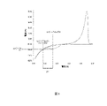
本発明の銅電気めっき組成物は、図1に示されるように、作用電極、好ましくは、Pt作用電極に関して収集されためっき槽のボルタンモグラムのカソード波における特有のα-ピーク曲線を示す。α-ピーク曲線のα-ピークが顕著であればあるほど、銅堆積物は一層異方性である。図1に示されるようなα-ピーク又はα-Peak I最大は、α-ピーク曲線の頂点にある。異方性成長をもたらす傾向は、図1に示されるように、ΔVを計算することによって定量化される。ΔV=α-Peak ImaxについてのV2-α-Peak ImaxのVである、ここで、α-Peak ImaxについてのV2は、図1の第2垂直点線によって示されるようなα-ピーク曲線の頂点での電圧又は電位であり、α-Peak ImaxのVは、α-ピーク曲線の頂点からの水平点線が、第1垂直点線によって図1にまた図示されるようなカソード波と交差する電圧である。 The copper electroplating composition of the present invention shows a unique α-peak curve in the cathode wave of the voltanmogram of the plating tank collected for the working electrode, preferably the Pt working electrode, as shown in FIG. The more prominent the α-peak of the α-peak curve, the more anisotropic the copper deposit. The α-peak or α-Peek I maximum as shown in FIG. 1 is at the apex of the α-peak curve. The tendency to result in anisotropic growth is quantified by calculating ΔV, as shown in FIG. ΔV = V 2 -α-Peak I max for α-Peak I max , where V 2 for α-Peak I max is α- as indicated by the second vertical dotted line in FIG. The voltage or potential at the apex of the peak curve, where the V of α-Peak I max is the horizontal dotted line from the apex of the α-peak curve with the cathode wave as also illustrated in FIG. 1 by the first vertical dotted line. The intersecting voltages.
異方性銅堆積物のめっきを可能にするための銅電気めっき組成物用のサプレッサーを選択するために、上に記載されたようなボルタンモグラムのカソード波におけるα-ピーク曲線が好ましくは用いられる。それらのサプレッサー活性について公知の様々な化合物をテストして異方性銅堆積物を可能にするそれらの能力を測定することができる。サプレッサーを含有する銅電気めっき組成物が、カソード波におけるα-ピーク曲線を持ったボルタンモグラフ曲線を提供する場合、そのサプレッサーは、異方性銅堆積物を電気めっきするために使用することができる。ΔVが大きければ大きいほど、特定のサプレッサーを使った銅電気めっき組成物からめっきされる銅堆積物は一層異方性である。 The α-peak curve in the cathode wave of the voltanmogram as described above is preferably used to select a suppressor for the copper electroplating composition to allow plating of anisotropic copper deposits. Various known compounds can be tested for their suppressor activity to measure their ability to enable anisotropic copper deposits. If the copper electroplating composition containing the suppressor provides a voltanmographic curve with an α-peak curve in the cathode wave, the suppressor can be used to electroplat the anisotropic copper deposits. The greater ΔV, the more anisotropic the copper deposits plated from the copper electroplating composition with a particular suppressor.
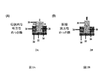
図2A及び2Bは、従来の銅電気めっき槽の等方性堆積銅線対本発明の異方性銅電気めっき槽から電気めっきされた銅線を図示し、比較している。図2Aは、銅シード層22でコートされた、シリコンウェハーなどの、誘電体基材20を図示する。画像形成フォトレジスト24がシード層22をコートしている。異方性銅線26は、画像形成フォトレジストにおける凹部28内に堆積して示されている。3つの矢印は、銅ピラーの成長及びその等方性キャラクターを示しており、ここで、線の区画は画像形成フォトレジスト24と重なっており、水平方向の銅堆積を示している。垂直矢印は、水平成長と同時に垂直方向の銅成長を示している。対照的に、図2Bは、銅シード層32でコートされた、シリコンウェハーなどの、誘電体基材30を図示する。画像形成フォトレジスト34がシード層32をコートしている。異方性銅ピラー36は、画像形成フォトレジストにおける凹部38内に堆積して示されている。垂直矢印は、いったん銅成長が画像形成フォトレジストの高さを越えると、銅堆積が水平方向にのみ起こっている銅ピラー36の異方性キャラクターを示している。画像形成フォトレジスト34一面の水平銅成長は、全くない。
2A and 2B illustrate and compare isotropically deposited copper wire in a conventional copper electroplating tank vs. copper wire electroplated from the anisotropic copper electroplating tank of the present invention. FIG. 2A illustrates a
本発明の異方性銅電気めっき組成物は、水性系であり、銅イオンの供給源を含む。銅イオン供給源は銅塩であり、硫酸銅;塩化銅などの銅ハロゲン化物;酢酸銅;硝酸銅;フルオロホウ酸銅;銅アルキルスルホネート;銅アリールスルホネート;スルファミン酸銅;及びグルコン酸銅が含まれるが、それらに限定されない。例示的な銅アルキルスルホネートには、銅(C1~C6)アルキルスルホネート及び銅(C1~C3)アルキルスルホネートが含まれる。好ましくは、銅アルキルスルホネートは、銅メタンスルホネート、銅エタンスルホネート及び銅プロパンスルホネートである。例示的な銅アリールスルホネートには、銅フェニルスルホネート、銅フェノールスルホネート及び銅p-トルエンスルホネートが含まれるが、それらに限定されない。銅イオン供給源の混合物を使用することができる。 The anisotropic copper electroplating composition of the present invention is an aqueous system and contains a source of copper ions. Copper ion sources are copper salts, including copper sulfate; copper halides such as copper chloride; copper acetate; copper nitrate; copper fluoroborate; copper alkyl sulfonates; copper aryl sulfonates; copper sulfamate; and copper gluconate. However, it is not limited to them. Exemplary copper alkyl sulfonates include copper (C 1 to C 6 ) alkyl sulfonates and copper (C 1 to C 3 ) alkyl sulfonates. Preferably, the copper alkyl sulfonates are copper methane sulfonate, copper ethane sulfonate and copper propane sulfonate. Exemplary copper aryl sulfonates include, but are not limited to, copper phenyl sulfonate, copper phenol sulfonate and copper p-toluene sulfonate. A mixture of copper ion sources can be used.
銅塩は、基材上に銅を電気めっきするための十分な銅イオン濃度を提供する量で、水性の異方性銅電気めっき槽に使用することができる。好ましくは、銅塩は、10g/L~180g/Lめっき液、より好ましくは、20g/L~100g/Lの銅イオンの量を提供するのに十分な量で存在する。 The copper salt can be used in an aqueous anisotropic copper electroplating tank in an amount that provides sufficient copper ion concentration for electroplating copper on a substrate. Preferably, the copper salt is present in an amount sufficient to provide an amount of 10 g / L to 180 g / L plating solution, more preferably 20 g / L to 100 g / L of copper ions.
酸を異方性銅電気めっき槽中に含めることができる。酸には、硫酸、フルオロホウ酸、アルカンスルホン酸、例えばメタンスルホン酸、エタンスルホン酸、プロパンスルホン酸及びトリフルオロメタンスルホン酸、アリールスルホン酸、例えばフェニルスルホン酸、フェノールスルホン酸及びトルエンスルホン酸、スルファミン酸、塩酸、並びにリン酸が含まれるが、それらに限定されない。酸の混合物を銅電気めっき槽に使用することができる。好ましくは、酸には、硫酸、メタンスルホン酸、エタンスルホン酸、プロパンスルホン酸、及びそれらの混合物が含まれる。 The acid can be included in the anisotropic copper electroplating tank. Acids include sulfuric acid, fluoroboric acid, alkane sulfonic acid, such as methane sulfonic acid, ethane sulfonic acid, propane sulfonic acid and trifluoromethane sulfonic acid, aryl sulfonic acid, such as phenyl sulfonic acid, phenol sulfonic acid and toluene sulfonic acid, sulfamic acid. , Hydrochloride, as well as phosphoric acid, but not limited to them. A mixture of acids can be used in copper electroplating tanks. Preferably, the acid includes sulfuric acid, methanesulfonic acid, ethanesulfonic acid, propanesulfonic acid, and mixtures thereof.
酸は、好ましくは、1g/L~300g/L、より好ましくは、5g/L~250g/L、さらに好ましくは、10~150g/Lの量で存在する。酸は、一般に、様々な供給元から市販されており、さらなる精製なしに使用することができる。 The acid is preferably present in an amount of 1 g / L to 300 g / L, more preferably 5 g / L to 250 g / L, still more preferably 10 to 150 g / L. Acids are generally commercially available from various sources and can be used without further purification.
ハロゲン化物イオンの供給源を異方性銅電気めっき槽中に含めることができる。ハロゲン化物イオンは、好ましくは塩化物イオンである。塩化物イオンの好ましい供給源は、塩化水素である。塩化物イオン濃度は、1ppm~100ppm、より好ましくは、10~100ppm、さらに好ましくは、20~75ppmの量にある。 The source of the halide ion can be included in the anisotropic copper electroplating tank. The halide ion is preferably a chloride ion. A preferred source of chloride ions is hydrogen chloride. The chloride ion concentration is in an amount of 1 ppm to 100 ppm, more preferably 10 to 100 ppm, still more preferably 20 to 75 ppm.
促進剤には、3-メルカプト-プロピルスルホン酸及びそのナトリウム塩、2-メルカプト-エタンスルホン酸及びそのナトリウム塩、及びビススルホプロピルジスルフィド及びそのナトリウム塩、3-(ベンゾチアゾリル-2-チオ)-プロピルスルホン酸ナトリウム塩、3-メルカプトプロパン-1-スルホン酸ナトリウム塩、エチレンジチオジプロピルスルホン酸ナトリウム塩、ビス-(p-スルホフェニル)-ジスルフィド二ナトリウム塩、ビス-(ω-スルホブチル)-ジスルフィド二ナトリウム塩、ビス-(ω-スルホヒドロキシプロピル)-ジスルフィド二ナトリウム塩、ビス-(ω-スルホプロピル)-ジスルフィド二ナトリウム塩、ビス-(ω-スルホプロピル)-スルフィド二ナトリウム塩、メチル-(ω-スルホプロピル)-ジスルフィドナトリウム塩、メチル-(ω-スルホプロピル)-トリスルフィド二ナトリウム塩、O-エチル-ジチオ炭酸-S-(ω-スルホプロピル)-エステル、カリウム塩チオグリコール酸、チオリン酸-O-エチル-ビス-(ω-スルホプロピル)-エステル二ナトリウム塩、チオリン酸-トリス(ω-スルホプロピル)-エステル三ナトリウム塩、N,N-ジメチルジチオカルバミン酸(3-スルホプロピル)エステル、ナトリウム塩、(O-エチルジチオカルボナト)-S-(3-スルホプロピル)-エステル、カリウム塩、3-[(アミノ-イミノメチル)-チオ]-1-プロパンスルホン酸並びに3-(2-ベンゾチアゾリルチオ)-1-プロパンスルホン酸、ナトリウム塩が含まれるが、それらに限定されない。好ましくは、促進剤は、ビススルホプロピルジスルフィド又はそのナトリウム塩である。好ましくは、促進剤は、1ppb~500ppm、より好ましくは50ppb~50ppm、最も好ましくは、5ppmから40ppmの量で銅電気めっき槽中に含まれる。 Accelerators include 3-mercapto-propyl sulfonic acid and its sodium salt, 2-mercapto-ethane sulfonic acid and its sodium salt, and bissulfopropyl disulfide and its sodium salt, 3- (benzothiazolyl-2-thio) -propyl. Sulfonic acid sodium salt, 3-mercaptopropane-1-sulfonic acid sodium salt, ethylenedithiodipropylsulfonic acid sodium salt, bis- (p-sulfophenyl) -disulfide disodium salt, bis- (ω-sulfobutyl) -disulfidedi Sodium salt, bis- (ω-sulfohydroxypropyl) -disulfide disodium salt, bis- (ω-sulfopropyl) -disulfide disodium salt, bis- (ω-sulfopropyl) -sulfide disodium salt, methyl- (ω) -Sulfonic acid) -disulfide sodium salt, methyl- (ω-sulfopropyl) -trisulfide disodium salt, O-ethyl-dithiocarbonate-S- (ω-sulfopropyl) -ester, potassium salt thioglycolic acid, thiophosphate -O-ethyl-bis- (ω-sulfopropyl) -ester disodium salt, thiophosphate-tris (ω-sulfopropyl) -ester trisodium salt, N, N-dimethyldithiocarbamic acid (3-sulfopropyl) ester, Sodium salt, (O-ethyldithiocarbonato) -S- (3-sulfopropyl) -ester, potassium salt, 3-[(amino-iminomethyl) -thio] -1-propanesulfonic acid and 3- (2-benzo Thiazolylthio) -1-propanesulfonic acid, including but not limited to sodium salts. Preferably, the accelerator is bissulfopropyl disulfide or a sodium salt thereof. Preferably, the accelerator is contained in the copper electroplating tank in an amount of 1 ppb to 500 ppm, more preferably 50 ppb to 50 ppm, most preferably 5 ppm to 40 ppm.
好ましくは、サプレッサーには、1000~6000g/モルの重量平均分子量を有するポリエチレングリコールポリマー、1000~5000g/モルの重量平均分子量を有するランダム及びブロックエチレンオキシド-プロピレンオキシド(「EO/PO」)コポリマーが含まれるが、それらに限定されない。 Preferably, the suppressor comprises a polyethylene glycol polymer having a weight average molecular weight of 1000-6000 g / mol, a random and blocked ethylene oxide-propylene oxide (“EO / PO”) copolymer having a weight average molecular weight of 1000-5000 g / mol. However, it is not limited to them.
より好ましくは、サプレッサーは、式中、変数x、x’、x’’、x’’’、y、y’、y’’及びy’’’が、コポリマーの重量平均分子量が1000~10,000g/モルの範囲であるような1以上の整数である、一般式:


を、好ましくは有する、ジアミンコア-EO/PO界面活性剤である。
More preferably, the suppressor has variables x, x', x'', x''', y, y', y'' and y''' in the formula, and the weight average molecular weight of the copolymer is 1000 to 10. An integer greater than or equal to 1 such as in the range of 000 g / mol, general formula:
Is preferably a diamine core-EO / PO surfactant.
1~4つのスルホン酸基末端のジアミン-コアポリマーが最も好ましい。最も好ましい例は、一般式:

を有するジアミン-コアポリマーである。
Most preferred are diamine-core polymers with 1 to 4 sulfonic acid groups. The most preferable example is the general formula:
It is a diamine-core polymer having.
サプレッサーは、好ましくは、0.5g/L~20g/L、より好ましくは、1g/L~10g/L、さらに好ましくは、1g/L~5g/Lの量で銅電気めっき槽中に含まれる。 The suppressor is preferably contained in the copper electroplating tank in an amount of 0.5 g / L to 20 g / L, more preferably 1 g / L to 10 g / L, still more preferably 1 g / L to 5 g / L. ..
好ましくは、レベラーには、イミダゾール及びブチルジグリシジルエーテル又はイミダゾール及びフェニルイミダゾールの反応生成物のコポリマーが含まれる。好ましくは、そのようなレベリング剤は、1000g/モル~50,000g/モルの重量平均分子量を有する。そのようなレベラーは、文献に開示されている方法によって又は当業者に公知の方法によって調製することができる。 Preferably, the leveler comprises a copolymer of imidazole and butyl diglycidyl ether or reaction product of imidazole and phenylimidazole. Preferably, such leveling agents have a weight average molecular weight of 1000 g / mol to 50,000 g / mol. Such levelers can be prepared by the methods disclosed in the literature or by methods known to those of skill in the art.
レベラーは、好ましくは、0.01ppm~100ppm、より好ましくは、0.01ppm~10ppm、さらに好ましくは、0.01ppm~1ppmの量で銅電気めっき槽中に含まれる。 The leveler is preferably contained in the copper electroplating tank in an amount of 0.01 ppm to 100 ppm, more preferably 0.01 ppm to 10 ppm, still more preferably 0.01 ppm to 1 ppm.
任意選択的に、所望のpHを維持するためにpH調整剤を組成物中に含めることができる。組成物のpHを調整するために1種以上の無機酸及び有機酸を含めることができる。無機酸には、硫酸、塩酸、硝酸及びリン酸が含まれるが、それらに限定されない。有機酸には、クエン酸、酢酸、アルカンスルホン酸、例えばメタンスルホン酸が含まれるが、それらに限定されない。組成物中に含めることができる塩基には、水酸化ナトリウム、水酸化カリウム、水酸化アンモニウム及びそれらの混合物が含まれるが、それらに限定されない。 Optionally, a pH regulator can be included in the composition to maintain the desired pH. One or more inorganic and organic acids can be included to adjust the pH of the composition. Inorganic acids include, but are not limited to, sulfuric acid, hydrochloric acid, nitric acid and phosphoric acid. Organic acids include, but are not limited to, citric acid, acetic acid, alcan sulfonic acid, such as methane sulfonic acid. Bases that can be included in the composition include, but are not limited to, sodium hydroxide, potassium hydroxide, ammonium hydroxide and mixtures thereof.
銅電気めっき組成物のpHは、0~14、好ましくは、0~6、より好ましくは、0~4の範囲である。 The pH of the copper electroplating composition is in the range of 0 to 14, preferably 0 to 6, and more preferably 0 to 4.
銅電気めっき用の導電性基材を提供するために、本発明の基材は、基材を導電性にするために、選択的に堆積させられたシード層、例えば銅シード層を含む。選択的に堆積させられたシード層は、次いで、選択的シード層上に異方性銅堆積物を提供するために銅めっきされる。いったんシード層が銅コートされると、継続的な銅めっきは、水平銅堆積が最小限~なしで垂直の銅成長をもたらす。或いは、基材の全表面は、シード層コーティングを含む。フォトレジスト材料がシード層一面に適用され、フォトレジストは、基材上にパターン又は特徴を形成するために当技術分野において公知の従来法を用いて画像形成される。フォトレジストは、当業者に公知の多くの従来型フォトレジストの1つであることができる。フォトレジストは、ネガ型又はポジ型フォトレジストであることができる。本発明の銅電気めっき組成物の異方性キャラクターのために、基材の表面に適用される任意のフォトレジストの厚さは、電気めっきされた銅層の厚さよりも薄いことができる。 To provide a conductive substrate for copper electroplating, the substrate of the present invention includes a seed layer selectively deposited, such as a copper seed layer, to make the substrate conductive. The selectively deposited seed layer is then copper plated to provide anisotropic copper deposits on the selective seed layer. Once the seed layer is copper coated, continuous copper plating results in vertical copper growth with minimal to no horizontal copper deposition. Alternatively, the entire surface of the substrate comprises a seed layer coating. A photoresist material is applied over one surface of the seed layer, and the photoresist is imaged using conventional methods known in the art to form patterns or features on the substrate. The photoresist can be one of many conventional photoresists known to those of skill in the art. The photoresist can be a negative or positive photoresist. Due to the anisotropic character of the copper electroplating composition of the present invention, the thickness of any photoresist applied to the surface of the substrate can be thinner than the thickness of the electroplated copper layer.
基材は、基材をめっき組成物と接触させることによって銅で電気めっきすることができる。基材は、カソードとして機能する。アノードは、可溶性又は不溶性アノードであることができる。十分な電流密度が適用され、めっきは、所望の厚さ及びモルフォロジを有する銅を基材上に堆積させるための時間の間行われる。電流密度は、0.5ASD~30ASD、好ましくは0.5ASD~20ASD、より好ましくは1ASD~10ASD、さらに好ましくは1ASD~5ASDの範囲であることができる。 The substrate can be electroplated with copper by contacting the substrate with the plating composition. The substrate functions as a cathode. The anode can be a soluble or insoluble anode. Sufficient current densities are applied and plating is carried out for a period of time for depositing copper with the desired thickness and morphology on the substrate. The current density can be in the range of 0.5 ASD to 30 ASD, preferably 0.5 ASD to 20 ASD, more preferably 1 ASD to 10 ASD, and even more preferably 1 ASD to 5 ASD.
電気めっき中の銅電気めっき槽の温度は、好ましくは、室温~65℃、より好ましくは、室温~35℃、さらに好ましくは、室温~30℃の範囲である。 The temperature of the copper electroplating tank during electroplating is preferably in the range of room temperature to 65 ° C, more preferably room temperature to 35 ° C, and even more preferably room temperature to 30 ° C.
本発明の銅電気めっき組成物及び方法は、幅が1~100μm、又は1~50μmなどの、又は1~5μmなどの及び高さが40μm以下の非等方的に細かい線を銅電気めっきすることができる。 The copper electroplating composition and method of the present invention copper electroplats asymmetrically fine wires having a width of 1 to 100 μm, a width of 1 to 50 μm, or a height of 1 to 5 μm and a height of 40 μm or less. be able to.
任意選択的に、しかし好ましくは、銅電気めっき前に、1種以上の硫黄含有促進剤化合物を含有する水性処理液でシード層を処理することができる。プレ銅電気めっき処理液は、さらに、異方性銅電気めっきを可能にする。処理液は、選択的に堆積させられたシード層に適用され、これに、異方性銅電気めっきが続く。水性処理液は、0~3未満などの、3未満のpH、又は9超~14などの、9超のpHを有する。 Optionally, but preferably, the seed layer can be treated with an aqueous treatment solution containing one or more sulfur-containing accelerator compounds prior to copper electroplating. The pre-copper electroplating treatment liquid further enables anisotropic copper electroplating. The treatment liquid is applied to the selectively deposited seed layer, followed by anisotropic copper electroplating. The aqueous treatment liquid has a pH of less than 3 such as 0 to less than 3, or a pH of more than 9 such as more than 9 to 14.
或いは、基材の全表面にシード層コーティングを含有する基材は、フォトレジストでコートし、画像形成してパターンを形成することができ、処理液がフォトレジストの画像形成区画の底部での露出シードと接触するように処理液を適用することができる。残存フォトレジストを、次いで、従来のフォトレジスト剥離剤で基材から剥離することができる。処理された銅シード層は、次いで、本発明の銅めっき組成物で銅めっきされる。非等方的銅電気めっきは、未処理のシード層ではなく、処理液で処理されたシード層上で起こる。任意選択的に、銅電気めっきは、処理液の適用後に、しかし、基材から画像形成フォトレジストを剥離する前に行うことができる。銅電気めっき後に、フォトレジストは、基材から剥離することができる。 Alternatively, the substrate containing the seed layer coating on the entire surface of the substrate can be coated with a photoresist to form an image to form a pattern, and the treatment liquid is exposed at the bottom of the image forming section of the photoresist. The treatment solution can be applied in contact with the seed. The residual photoresist can then be stripped from the substrate with a conventional photoresist stripper. The treated copper seed layer is then copper plated with the copper plating composition of the present invention. Anisotropy copper electroplating occurs on the seed layer treated with the treatment liquid, not on the untreated seed layer. Optionally, copper electroplating can be performed after application of the treatment solution, but before stripping the image-forming photoresist from the substrate. After copper electroplating, the photoresist can be stripped from the substrate.
硫黄含有促進剤には、本発明の銅電気めっき組成物に含まれる促進剤の多くが含まれる。促進剤には、3-メルカプト-プロピルスルホン酸及びそのナトリウム塩、2-メルカプト-エタンスルホン酸及びそのナトリウム塩、及びビススルホプロピルジスルフィド及びそのナトリウム塩、3-(ベンゾチアゾイル-2-チオ)-プロピルスルホン酸ナトリウム塩、3-メルカプトプロパン-1-スルホン酸ナトリウム塩、エチレンジチオジプロピルスルホン酸ナトリウム塩、ビス-(p-スルホフェニル)-ジスルフィド二ナトリウム塩、ビス-(ω-スルホブチル)-ジスルフィド二ナトリウム塩、ビス-(ω-スルホヒドロキシプロピル)-ジスルフィド二ナトリウム塩、ビス-(ω-スルホプロピル)-ジスルフィド二ナトリウム塩、ビス-(ω-スルホプロピル)-スルフィド二ナトリウム塩、メチル-(ω-スルホプロピル)-ジスルフィドナトリウム塩、メチル-(ω-スルホプロピル)-トリスルフィド二ナトリウム塩、O-エチル-ジチオ炭酸-S-(ω-スルホプロピル)-エステル、カリウム塩チオグリコール酸、チオリン酸-O-エチル-ビス-(ω-スルホプロピル)-エステル二ナトリウム塩、チオリン酸-トリス(ω-スルホプロピル)-エステル三ナトリウム塩、N,N-ジメチルジチオカルバミン酸(3-スルホプロピル)エステル、ナトリウム塩、(O-エチルジチオカルボナト)-S-(3-スルホプロピル)-エステル、カリウム塩、3-[(アミノ-イミノメチル)-チオ]-1-プロパンスルホン酸並びに3-(2-ベンゾチアゾリルチオ)-1-プロパンスルホン酸、ナトリウム塩が含まれるが、それらに限定されない。好ましくは、促進剤は、2-メルカプト-エタンスルホン酸及びそのナトリウム塩である。好ましくは、促進剤は、1ppb~500ppm、より好ましくは50ppb~50ppm、最も好ましくは、5ppm~40ppmの量で銅電気めっき槽中に含まれる。 The sulfur-containing accelerator contains many of the accelerators contained in the copper electroplating composition of the present invention. Accelerators include 3-mercapto-propyl sulfonic acid and its sodium salt, 2-mercapto-ethane sulfonic acid and its sodium salt, and bissulfopropyl disulfide and its sodium salt, 3- (benzothiazoyl-2-thio). -Sodium propylsulfonic acid salt, 3-mercaptopropane-1-sodium sulfonic acid salt, sodium ethylenedithiodipropylsulfonic acid salt, bis- (p-sulfophenyl) -dissulfide disodium salt, bis- (ω-sulfobutyl)- Disulfide disodium salt, bis- (ω-sulfohydroxypropyl) -disulfide disodium salt, bis- (ω-sulfopropyl) -disulfide disodium salt, bis- (ω-sulfopropyl) -sulfide disodium salt, methyl- (Ω-sulfopropyl) -disulfide sodium salt, methyl- (ω-sulfopropyl) -trisulfide disodium salt, O-ethyl-dithiocarbonate-S- (ω-sulfopropyl) -ester, potassium salt thioglycolic acid, Thiophosphate-O-ethyl-bis- (ω-sulfopropyl) -ester disodium salt, thiophosphate-tris (ω-sulfopropyl) -ester trisodium salt, N, N-dimethyldithiocarbamic acid (3-sulfopropyl) Estel, sodium salt, (O-ethyldithiocarbonato) -S- (3-sulfopropyl) -ester, potassium salt, 3-[(amino-iminomethyl) -thio] -1-propanesulfonic acid and 3- (2) -Benzothiazolylthio) -1-Propane sulfonic acid, including but not limited to sodium salts. Preferably, the accelerator is 2-mercapto-ethanesulfonic acid and a sodium salt thereof. Preferably, the accelerator is contained in the copper electroplating tank in an amount of 1 ppb to 500 ppm, more preferably 50 ppb to 50 ppm, and most preferably 5 ppm to 40 ppm.
任意選択的に、1種以上の界面活性剤を本発明の処理液中に含めることができる。そのような界面活性剤には、非イオン界面活性剤、カチオン界面活性剤、アニオン界面活性剤及び両性界面活性剤が含まれる。例えば、非イオン界面活性剤には、ポリエステル、ポリエチレンオキシド、ポリプロピレンオキシド、アルコール、エトキシレート、シリコン化合物、ポリエーテル、グリコシド及びそれらの誘導体が含まれることができ;アニオン界面活性剤には、アニオン性カルボン酸塩又は有機硫酸塩、例えばラウリルエーテル硫酸ナトリウム(SLES)が含まれることができる。 Optionally, one or more surfactants can be included in the treatment liquid of the present invention. Such surfactants include nonionic surfactants, cationic surfactants, anionic surfactants and amphoteric surfactants. For example, nonionic surfactants can include polyesters, polyethylene oxides, polypropylene oxides, alcohols, ethoxylates, silicon compounds, polyethers, sulfates and derivatives thereof; anionic surfactants are anionic. Carboxylates or organic sulfates, such as sodium lauryl ether sulfate (SLES), can be included.
界面活性剤は、従来の量で含まれることができる。好ましくは、界面活性剤が本発明の処理液中に含まれるとき、それらは、0.1g/L~10g/Lの量で含まれる。 The surfactant can be included in conventional amounts. Preferably, when the surfactants are included in the treatment liquid of the present invention, they are included in an amount of 0.1 g / L to 10 g / L.
本発明の処理液は、室温~60℃、好ましくは、室温~30℃の温度で適用することができ、より好ましくは、組成物は室温で銅に適用される。 The treatment liquid of the present invention can be applied at a temperature of room temperature to 60 ° C., preferably room temperature to 30 ° C., and more preferably the composition is applied to copper at room temperature.
本発明の処理液は、シード層を持った基材を溶液中に浸漬することによって、溶液を基材上に噴霧することによって、又は溶液を基材に適用するための他の従来の方法によって適用することができる。本発明の処理液は、また、銅に選択的に適用することができる。選択的な適用は、溶液を基材に選択的に適用するための任意の従来法によって行うことができる。そのような選択的な適用には、インクジェット適用、ライティングペン、アイドロッパー、パターン化表面を有するポリマースタンプ、画像形成フォトレジストによるなどのマスク又はスクリーン印刷が含まれるが、それらに限定されない。 The treatment liquid of the present invention is obtained by immersing a substrate having a seed layer in the solution, by spraying the solution onto the substrate, or by another conventional method for applying the solution to the substrate. Can be applied. The treatment liquid of the present invention can also be selectively applied to copper. Selective application can be performed by any conventional method for selectively applying the solution to the substrate. Such selective applications include, but are not limited to, inkjet applications, writing pens, eye droppers, polymer stamps with patterned surfaces, masks or screen printing such as with image forming photoresists.
図3は、処理液の適用を伴った本発明の方法及び本発明の方法に従って堆積させられた異方性銅線を図示する。基材40は、銅シード層42でコートされ、銅シード層は、開口部46を持った3μmの高さを有する画像形成フォトレジスト44でコートされている。開口部46の底部での露出シード層48の区画は、処理シード層50を提供するためにMESを含有する処理液で処理される。フォトレジストは、次いで、剥離されて処理シード層50を残す。処理シード層は、次いで、本発明の異方性銅電気めっき槽でめっきされ、ここで、銅線成長は、処理液で処理されたシード層上でのみ垂直に起こり、そのとき残りの銅成長は等方性であり、銅線52を形成する。
FIG. 3 illustrates the method of the invention with the application of the treatment solution and the anisotropic copper wire deposited according to the method of the invention. The
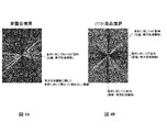
図4A及び4Bは、異方性銅か等方性銅かかのどちらかで電気めっきされた線特徴の横断面の粒界解析の分析による非等方的にめっきされた銅の構造を図示する。図4Aは、非等方的に成長した線特徴(白線)マイナス等方的に成長した線特徴(黒線)の差フーリエ変換マップであり、基材に対する非コヒレント粒子境界の配向を示す。白い水平線は、非等方的に成長した線のこれらの境界が、基材に対して90°で優先的に配向していることを示し、それは、それらがめっきされた銅の沿面成長を削減し、こうして異方性めっき成長を確実にしていることを示唆している。図4Bは、非等方的に成長した線特徴マイナス等方的に成長した線特徴の類似の差フーリエ変換マップであり、基材に対する(111)-双晶粒子境界の配向を示す。2つの白い対角線は、非等方的に成長した線の双晶境界が、基材に対して約45°で配向していることを示し、それは、非整合境界の領域内の粒子成長が(111)-双晶平面一面への堆積によって起こることを示唆している。 4A and 4B illustrate the structure of isotropically plated copper by analysis of grain boundary analysis of cross-sections of wire features electroplated with either anisotropic copper or isotropic copper. do. FIG. 4A is a differential Fourier transform map of non-isotropically grown line features (white lines) minus isotropically grown line features (black lines), showing the orientation of non-coherent particle boundaries with respect to the substrate. The white horizon indicates that these boundaries of the anisotropically grown line are preferentially oriented at 90 ° with respect to the substrate, which reduces the creepage growth of the copper on which they are plated. Thus, it is suggested that the anisotropic plating growth is ensured. FIG. 4B is a similar difference Fourier transform map of non-isotropically grown line features minus isotropically grown line features showing the orientation of the (111) -twinned particle boundary with respect to the substrate. The two white diagonals indicate that the twinned boundaries of the non-isotropically grown lines are oriented at about 45 ° with respect to the substrate, which means that the particle growth within the region of the unmatched boundaries is ( 111) -It is suggested that it is caused by the deposition on one surface of the twin plane.
本発明の物品は、特徴広がりをもたらすことなく、周囲のフォトレジストの高さの少なくとも2μm上方にめっきされている、及び基材の平面に対して80~90°で配向した非整合境界を含み、且つ、基材の平面に対して40~50°で配向した並行の双晶境界を含む銅堆積物を含む。 Articles of the invention include non-matching boundaries that are plated at least 2 μm above the height of the surrounding photoresist without causing feature spread and oriented at 80-90 ° with respect to the plane of the substrate. It also contains copper deposits containing parallel bicrystal boundaries oriented at 40-50 ° with respect to the plane of the substrate.
以下の実施例は、本発明をさらに例示するために含まれるが、その範囲を限定することを意図しない。 The following examples are included to further illustrate the invention, but are not intended to limit its scope.
実施例1~2
活性化なし等方性槽1に対して高異方性槽3での3-メルカプト-プロピルスルホン酸ナトリウム塩活性化1~100μm細線パターンに関するめっき高さレベリング
以下の2つの銅電気めっき槽を調製した:
めっき槽1(等方性槽):
50g/LのCu(II)イオン
100g/LのH2SO4
50ppmの塩化物イオン
5ppmのビス-ナトリウム-スルホプロピル-ジスルフィド
2g/Lの平均MW 1,100及びヒドロキシル末端基のEO-POランダムコポリマー
5ppmのエピクロロヒドリン及びイミダゾールの反応生成物
めっき槽2(異方性槽):
50g/LのCu(II)イオン
100g/LのH2SO4
50ppmの塩化物イオン
40ppmのビス-ナトリウム-スルホプロビル-ジスルフィド
2g/Lの平均MW 1,100及びヒドロキシル末端基のEO-POランダムコポリマー
1ppmのブチルジグリシジルエーテル、イミダゾール及びフェニルイミダゾールの反応生成物
めっき槽3(異方性槽):
50g/LのCu(II)イオン
100g/LのH2SO4
50ppmの塩化物イオン
20ppmのビス-ナトリウム-スルホプロビル-ジスルフィド
2g/Lの及び7,000の平均MWのEO-POブロックコポリマー
0.1ppmのブチルジグリシジルエーテル、イミダゾール及びフェニルイミダゾールの反応生成物
Examples 1-2
Plating height leveling for 3-mercapto-propylsulfonic acid sodium salt activation 1-100 μm fine wire pattern in highly anisotropic tank 3 with respect to
Plating tank 1 (isotropic tank):
50 g / L Cu (II) ion 100 g / L H 2 SO 4
50 ppm chloride ion 5 ppm bis-sodium-sulfopropyl-disulfide 2 g / L average MW 1,100 and hydroxyl end group EO-PO random copolymer 5 ppm epichlorohydrin and imidazole reaction product Plating tank 2 ( Anisotropic tank):
50 g / L Cu (II) ion 100 g / L H 2 SO 4
50
50 g / L Cu (II) ion 100 g / L H 2 SO 4
50
20nmのTi接着層及び200nmの導電性Cuシードでコートされたシリコンウェハーを、3μmの厚さのポジ型Shipley BPRTM 100 PR層と積層した。幅が6~100μmの範囲の一連の溝を含有するために細線パターンをPR層上に構築した。これらの溝を、次いで、めっき槽1かめっき槽3かのどちらかを使用して4.5μmのターゲット高さまでめっきした。めっき槽1でめっきされるサンプルは、めっき前にDI水で濡らした。めっき槽3でめっきされるサンプルは、めっき前に、先ず、水中の4g/LのMESのpH 0.7の溶液中に浸漬し、次いでDI水でリンスした。両方の場合に、電気めっきを、50rpmのカソード回転速度で、2ASDで実施した。めっき後に、80℃で10分間Shipley BPRTM Stripperを使用してPRを除去して細線のパターンをもたらした。次いで、84mL/Lの85%リン酸及び8mL/Lの45.5%過酸化水素を含有するエッチ液にサンプルを曝露して、PRによって保護されていた残存導電性シードを除去した。Keyence Corporation製のレーザー表面形状測定装置を用いて孤立Cu細線の高さを測定した。表1にまとめられた、結果は、特徴サイズの変化にもかかわらず、めっき高さが一様である、高度に同じレベルにされた堆積物を両めっき槽が生成することを示した。これらの結果は、異方性めっきが、めっき槽1によって典型的に提供されるような、広範囲の線サイズにわたって高度に同じレベルにされた堆積物を依然として達成しながら可能であることを示した。
A silicon wafer coated with a 20 nm Ti adhesive layer and a 200 nm conductive Cu seed was laminated with a 3 μm thick positive Shipley BPR TM 100 PR layer. A fine line pattern was constructed on the PR layer to contain a series of grooves with a width in the range of 6-100 μm. These grooves were then plated using either

実施例3~6.
活性化なし非界面反応性槽1に対して、高界面反応性槽2でのMES活性化1~100μm細線パターンに関する線広がり
20nmのTi接着層及び200nmの導電性Cuシードでコートされたシリコンウェハーを、3μmの厚さのPR層と積層した。幅が1~100μmの範囲の一連の溝を含有するために細線パターンをPR層上に構築した。これらの溝を、次いで、めっき槽1かめっき槽2かのどちらかを使用して4.5μmのターゲット高さまでめっきした。各場合に、サンプルを、めっき前にDI水で濡らすか、それともそれらを先ず、めっき前に水中の4g/LのMESのpH 0.7の溶液中に浸漬し、次いでDI水でリンスした。全ての場合に、電気めっきを、50rpmのカソード回転速度で、2ASDで実施した。めっき後に、PRを、PR剥離剤浴中で除去して細線のパターンをもたらした。サンプルを、次いで、シードエッチ液に曝露して、PRによって保護されていた残存導電性シードを除去した。レーザー表面形状測定装置を用いて孤立Cu細線の幅を測定した。表2にまとめられた、結果は、ターゲットめっき高さがPR層の高さのかなり上方であるけれども、めっき槽3が著しい線広がりを防ぐことを示した。その一方で、めっき槽1で調製されたサンプルは、いかなる前処理にもかかわらず、著しい線広がりを示した。線ピッチが小さいサンプルのエリアにおいて、この広がりは、隣接Cu線の融合をもたらした。
Examples 3-6.
A silicon wafer coated with a 20 nm Ti adhesive layer and a 200 nm conductive Cu seed for a non-interfacial

実施例7~10
活性化なし非界面反応性槽1に対して、高界面反応性槽3でのMES活性化1~100μm細線パターンに関する線広がり
20nmのTi接着層及び200nmの導電性Cuシードでコートされたシリコンウェハーを、3μmの厚さのPR層と積層した。一連の100μ幅の溝を包含するために細線パターンをPR層上に構築した。基材を、次いで、めっき槽1かめっき槽3かのどちらかを使用して36μmのターゲット高さまでめっきした。めっき槽1でめっきされるサンプルは、めっき前にDI水で濡らした。めっき槽3でめっきされるサンプルは、先ず、めっき前に水中の4g/LのMESのpH 0.7の溶液中に浸漬し、次いでDI水でリンスした。両方の場合に、電気めっきを、50rpmのカソード回転速度で、2ASDで実施した。めっき後に、PRを、PR剥離剤浴中で除去して細線のパターンをもたらした。サンプルを次いでSEMによって画像化した。表3は、めっき槽1でめっきされたサンプルが完全な線融合をもたらし、一方、めっき槽3でめっきされたサンプルが、いかなる有意の線広がりをも示さず、めっきされた堆積物がより薄いPRパターンの形状に従って非等方的に成長していることを示す。
Examples 7-10
A silicon wafer coated with a 20 nm Ti adhesive layer and a 200 nm conductive Cu seed for a non-interfacial
細線パターンを、次いで、1~5μmの範囲の幅の一連の溝を含有するために類似の基材の3μmのPR層上に構築した。この基材を、次いで、ただ一つの違いが6μmのより低いめっきターゲットである状態で、上記と同じプロセスフローを用いて同様にめっきした。表3は、めっき槽1でめっきされたサンプルが完全な線融合をもたらし、一方、めっき槽3でめっきされたサンプルが、いかなる有意の線広がりをも示さず、めっきされた堆積物がより薄いPRパターンの形状に従って非等方的に成長したことを示す。
A fine line pattern was then constructed on a 3 μm PR layer of a similar substrate to contain a series of grooves with a width in the range of 1-5 μm. This substrate was then similarly plated using the same process flow as above, with the only difference being the lower plating target of 6 μm. In Table 3, the samples plated in the

実施例11~18.
100μm幅の線に対する異なるめっき槽での界面活性化対無界面活性化の影響
20nmのTi接着層及び200nmの導電性Cuシードでコートされたシリコンウェハーを、3μmの厚さのPR層と積層した。一連の100μ幅の溝を含有するために細線パターンをPR層上に構築した。基材を、次いで、4つの異なるめっき槽調合物を使用して6μmのターゲット高さまでめっきした。各場合に、サンプルを、めっき前にDI水で濡らすか、それともそれらを先ず、めっき前に水中の4g/LのMESのpH 0.7の溶液中に浸漬し、次いでDI水でリンスした。全ての場合に、電気めっきを、50rpmのカソード回転速度で、10ASDで実施した。めっき後に、PRを、PR剥離剤浴中で除去して細線のパターンをもたらした。サンプルを、次いで、樹脂成形し、アルゴンプラズマを使用して横断面切断した。これに、線形状及び一様性に対するめっき調合物の影響を観察するためのSEM撮像が続いた。結果のまとめは下記である。
Examples 11-18.
Effect of Surfactant vs. Non-surfactant in Different Plating Tanks on 100 μm Wide Lines A 20 nm Ti Adhesive Layer and a 200 nm Conductive Cu Seed Coated Silicon Wafer were laminated with a 3 μm thick PR layer. .. A fine line pattern was constructed on the PR layer to contain a series of 100 μ wide grooves. The substrate was then plated to a target height of 6 μm using four different plating tank formulations. In each case, the samples were either wetted with DI water prior to plating or they were first immersed in a solution of 4 g / L MES pH 0.7 in water prior to plating and then rinsed with DI water. In all cases, electroplating was performed at a cathode speed of 50 rpm and 10 ASD. After plating, PR was removed in a PR stripping agent bath to give a fine line pattern. The sample was then resin molded and cross-sectionally cut using argon plasma. This was followed by SEM imaging to observe the effect of the plating formulation on linear shape and uniformity. The summary of the results is as follows.
実施例11及び12は、めっき槽3でめっきした。実施例11は、MES溶液で前処理し、一方、実施例12は、DI水でプレ湿潤したのみであった。実施例11は、均一な線形状及び線のエッジに沿った異方性成長を示した。実施例12は、ひどく不均一な線形状及び線のエッジに沿った異方性成長をもたらす。 Examples 11 and 12 were plated in the plating tank 3. Example 11 was pretreated with MES solution, while Example 12 was only pre-wet with DI water. Example 11 showed a uniform line shape and anisotropic growth along the edges of the line. Example 12 results in a severely non-uniform line shape and anisotropic growth along the edges of the line.
実施例13及び14は、めっき槽2でめっきした。実施例13は、MES溶液で前処理し、一方、実施例14は、DI水でプレ湿潤したのみであった。実施例13は、均一な線形状及び線のエッジに沿った穏やかに異方性の成長を示した。本明細書において、穏やかに異方性の槽は、めっき槽1よりも少ない線広がりを生み出す、及びPRの高さの上方にめっきする場合に基材に対して75~89°のめっき堆積物成長方向をもたらす調合物である。実施例14は、不均一な線形状及び線のエッジに沿った穏やかに異方性の成長を示した。
Examples 13 and 14 were plated in the plating tank 2. Example 13 was pretreated with MES solution, while Example 14 was only pre-wet with DI water. Example 13 showed a uniform line shape and gently anisotropic growth along the edges of the line. As used herein, a mildly anisotropic tank produces less line spread than plating
実施例15及び16は、
50g/LのCu(II)イオン
100g/LのH2SO4
50ppmの塩化物イオン
40ppmのビス-ナトリウム-スルホプロピル-ジスルフィド
2g/Lの、平均MW 1,100及びヒドロキシル末端基のEO-POブロックコポリマー
1ppmの、ブチルジグリシジルエーテル、イミダゾール及びフェニルイミダゾールの反応生成物
を含有する、めっき槽4でめっきした。
Examples 15 and 16 are
50 g / L Cu (II) ion 100 g / L H 2 SO 4
50
実施例15は、MES溶液で前処理し、一方、実施例16は、DI水でプレ湿潤したのみであった。実施例15は、均一な線形状及び線のエッジに沿って穏やかに等方性の成長を示した。穏やかに等方性の槽は、めっき槽1よりも少ない線広がりを生み出す、及びPRの高さの上方にめっきする場合に基材に対して40~74°のめっき堆積物成長方向をもたらす調合物である。実施例14は、不均一線形状及び線のエッジに沿った等方性の成長を示した。
Example 15 was pretreated with MES solution, while Example 16 was only pre-wet with DI water. Example 15 showed a uniform line shape and gently isotropic growth along the edges of the line. The mildly isotropic tank produces less line spread than the
実施例17及び18は、めっき槽1でめっきした。実施例17は、MES溶液で前処理したが、一方。実施例18は、DI水でプレ湿潤したのみであった。実施例17は、均一な線形状及び線のエッジに沿った強く等方性の成長を示した。実施例18は、均一な線形状及び線のエッジに沿った強く等方性の成長を示した。
Examples 17 and 18 were plated in the
実施例11~18を、横断面切断し、次いでEBSDによって分析して、増加した異方性めっき挙動と一緒にもたらされる微細構造の差を測定した。この目的に向かって、各横断面における全ての境界の長さを分析し、相当する横断面表面積で割って境界密度を得た。こうして、めっき槽調合物の異方性成長挙動が目立てば目立つほど、双晶境界密度は、MES溶液でのシード活性化時に一層増加することが分かった。このトレンドを表4に示す。加えて、全てのサンプルがめっきの直後に小さい粒子のCu堆積物を含有するが、Cu粒子サイズが、めっき調合物に依存して室温において異なる速度で増加することが観察される。サンプルが横断面切断され、分析される時までに、高等方性成長実施例17~18の粒子サイズは、高異方性実施例11~12の粒子サイズよりも大きい。粒子成長は、双晶境界などの、安定した粒子境界が形成されるまで続き得る。これは、実施例17~18における比較的高い双晶密度が、高い双晶境界密度を生成するめっき槽1の固有の性向よりもむしろ、その後の粒子成長の結果として生じ得ることを示唆している。したがって、データは、めっき中に双晶境界を形成するより高い性向が、異方性成長に同伴することを示唆している。
Examples 11-18 were cross-sectionally cut and then analyzed by EBSD to measure the microstructure differences resulting with increased anisotropic plating behavior. To this end, the lengths of all boundaries in each cross section were analyzed and divided by the corresponding cross section surface area to obtain boundary densities. Thus, it was found that the more prominent the anisotropic growth behavior of the plating tank formulation, the more the twin boundary density increased during seed activation in the MES solution. This trend is shown in Table 4. In addition, although all samples contain small particles of Cu deposits immediately after plating, it is observed that the Cu particle size increases at different rates at room temperature depending on the plating formulation. By the time the sample is cross-sectionally cut and analyzed, the particle size of Highly Anisotropy Growth Examples 17-18 is larger than the particle size of Highly Anisotropy Examples 11-12. Particle growth can continue until a stable particle boundary, such as a twin boundary, is formed. This suggests that the relatively high twin densities in Examples 17-18 can occur as a result of subsequent particle growth rather than the inherent tendency of the

EBSDデータをフーリエ解析によってさらに処理して異方性成長に、基材に対する境界配向の変化が同伴するかどうかについて研究した。実施例11についてのフーリエ変換マップを、(111)-双晶境界に対して全ての非整合境界のいずれかに関して実施例18について4のマップで差し引いた。結果として生じる差マップを、図4A及び4Bに示す。水平線がめっき中の基材に垂直の境界配列を示すのに対して、垂直線は、平行の境界配列を示す。白線は、異方性成長実施例11における優先的配列に相当し、黒線は、等方性成長実施例18における優先的配列に相当する。データは、異方性成長に、基材に垂直の非整合境界の優先的配列が同伴し、一方、異方性成長が、不十分に画定された優先傾向と関連していることを示した。(111)-双晶境界の場合に、等方性成長サンプルは、垂直及び平行配向を示したのに対して、異方性サンプルは、基材に対して約45°で(111)-双晶境界の配向のほどほどの優先傾向を示した。 EBSD data were further processed by Fourier analysis to study whether anisotropic growth was accompanied by changes in boundary orientation with respect to the substrate. The Fourier transform map for Example 11 was subtracted from the map for Example 18 for any of all inconsistent boundaries with respect to the (111) -twin boundary. The resulting difference maps are shown in FIGS. 4A and 4B. The horizontal line shows the boundary arrangement perpendicular to the substrate being plated, while the vertical line shows the parallel boundary arrangement. The white line corresponds to the preferred sequence in anisotropic growth Example 11, and the black line corresponds to the preferred sequence in isotropic growth Example 18. The data showed that anisotropic growth was accompanied by a preferred sequence of unmatched boundaries perpendicular to the substrate, while anisotropic growth was associated with poorly defined priority trends. .. In the case of the (111) -twin boundary, the isotropic growth sample showed vertical and parallel orientation, whereas the anisotropic sample showed (111) -twin at about 45 ° to the substrate. The orientation of the crystal boundaries showed a moderate priority.
総合すれば、双晶境界密度及びフーリエ解析データは、異方性成長が、堆積を受ける又は双晶境界一面に新しい粒子の核となる優先傾向に由来することを示唆する。非整合境界一面への成長のより低い優先傾向は、これらの境界が堆積物を堆積物の厚さに沿って固定する傾向をもたらし、それが外側に伸びるのを防ぎ、こうして異方性成長をもたらす。その一方で、等方性サンプルにおける堆積物の厚さに沿って横方向に伸びる全ての境界の能力は、Cuが優先的な方向なしに成長する経路を提供する。 Taken together, twin boundary densities and Fourier analysis data suggest that anisotropic growth derives from the preferential tendency to undergo deposition or to nucleate new particles across the twin boundary. The lower priority tendency of growth to one side of the unconformity boundary results in the tendency of these boundaries to fix the sediment along the thickness of the deposit, preventing it from extending outwards and thus anisotropic growth. Bring. On the other hand, the ability of all boundaries extending laterally along the thickness of the deposit in the isotropic sample provides a pathway for Cu to grow without a preferred direction.
実施例19~25
界面活性化に応答する及びめっき成長角を高めるめっき槽の設計
めっき堆積物の成長角は、めっき組成物を変えることによって調整することができる。調合物における一つの重要な変数は、サプレッサー添加剤の選択である。したがって、線広がりに対するサプレッサーの影響を研究するために、
50g/LのCu(II)イオン
100g/LのH2SO4
50ppmの塩化物イオン
40ppmのビス-ナトリウム-スルホプロピル-ジスルフィド
0.1ppmのブチルジグリシジルエーテル、イミダゾール及びフェニルイミダゾールの反応生成物
2g/Lのサプレッサー添加剤
を含有する槽中へ異なるサプレッサー
実施例19:PEG MW 1,000
実施例20:ブロックEO-PO MW 1,100
実施例21:ブロックEO-PO MW 1,950
実施例22:ランダムEO/PO MW 1,100
実施例23:リバースTetronic MW 3,750
実施例24:リバースTetronic MW 5,300
実施例25:スルホン化末端基のリバースTetronic、MW 4,800
を組み入れた。
Pt回転作用電極(10rpm、10mV/sスキャン速度、25℃)、Cu電気めっき槽用の一般的な分析ツールを使用して図1に示されるような、サイクリック・ボルタンメトリーによって調合物を分析した。所与の調合物によって生成する異方性成長が目立てば目立つほど、CVSのカソード波におけるα-ピーク特徴が一層目立ったものになるであろうことが観察された。このようにして、異方性成長をもたらす傾向を、図1に示されるように、ΔVを計算することによって定量化した。実施例19からのめっき槽は、0.003VのΔVをもたらし;実施例20は、0.049VのΔVをもたらし;実施例21は、0.076VのΔVをもたらし;実施例22は、0.093VのΔVをもたらし;実施例23は、0.094VのΔVをもたらし;実施例24は、0.095VのΔVをもたらし;実施例25は、0.101VのΔVをもたらした。
Examples 19-25
Design of the plating tank that responds to surface activation and enhances the plating growth angle The growth angle of the plating deposit can be adjusted by changing the plating composition. One important variable in the formulation is the choice of suppressor additive. Therefore, to study the effect of suppressors on line spread,
50 g / L Cu (II) ion 100 g / L H 2 SO 4
50
Example 20: Block EO-PO MW 1,100
Example 21: Block EO-PO MW 1,950
Example 22: Random EO / PO MW 1,100
Example 23: Reverse Tetronic MW 3,750
Example 24: Reverse Tetronic MW 5,300
Example 25: Reverse Tetronic, MW 4,800 of sulfonated end groups
Was incorporated.
The formulations were analyzed by cyclic voltammetry as shown in FIG. 1 using a Pt rotating working electrode (10 rpm, 10 mV / s scan rate, 25 ° C.), a common analytical tool for Cu electroplating tanks. .. It was observed that the more prominent the anisotropic growth produced by a given formulation, the more prominent the α-peak characteristics in the cathode wave of CVS. In this way, the tendency to result in anisotropic growth was quantified by calculating ΔV, as shown in FIG. The plating tank from Example 19 yields a ΔV of 0.003V; Example 20 yields a ΔV of 0.049V; Example 21 yields a ΔV of 0.076V; Example 22 yields 0. Example 23 yielded a ΔV of 093V; Example 23 yielded a ΔV of 0.094V; Example 24 yielded a ΔV of 0.095V; Example 25 yielded a ΔV of 0.101V.
実施例26~35
異なるサプレッサー添加剤での1~60μm幅特徴パターンにおける特徴広がりの制御
20nmのTi接着層及び200nmの導電性Cuシードでコートされたシリコンウェハーを、3μmの厚さのPR層と積層した。幅が1~60μmの範囲の一連の溝を含有するために細線パターンをPR層上に構築した。これらの溝を、次いで、サプレッサー添加剤のアイデンティティが異なる10個の異なるめっき槽調合物を使用して6μmのターゲット高さまでめっきした:
50g/LのCu(II)イオン
100g/LのH2SO4
50ppmの塩化物イオン
40ppmのビス-ナトリウム-スルホプロピル-ジスルフィド
0.1ppmのブチルジグリシジルエーテル、イミダゾール及びフェニルイミダゾールの反応生成物
2g/Lのサプレッサー添加剤
実施例26:ブロックEO-PO MW 1,100
実施例27:ブロックEO-PO MW 1,950
実施例28:ブロックEO-PO MW 4,950
実施例29:ランダムEO/PO MW 1,100
実施例30:PEG MW 1,000
実施例31:PEG MW 6,000
実施例32:リバースTetronic MW 3,750
実施例33:リバースTetronic MW 5,300
実施例34:リバースTetronic MW 7,250
実施例35:スルホン化末端基のリバースTetronic、MW 4,800
各サンプルを、めっき前にDI水でリンスした。全ての場合に、電気めっきを、50rpmのカソード回転速度で、2ASDで実施した。めっき後に、PRを、PR剥離剤浴中で除去して細線のパターンをもたらした。サンプルを、次いで、Cu及びTiエッチ液に曝露して、PRによって保護されていた残存導電性シードを除去した。最後に、レーザー表面形状測定装置によってめっき線の幅を測定した。
Examples 26-35
Controlling Feature Spread in 1-60 μm Width Feature Patterns with Different Suppressor Additives A 20 nm Ti adhesive layer and a silicon wafer coated with 200 nm conductive Cu seeds were laminated with a 3 μm thick PR layer. A fine line pattern was constructed on the PR layer to contain a series of grooves with a width in the range of 1-60 μm. These grooves were then plated to a target height of 6 μm using 10 different plating tank formulations with different suppressor additive identities:
50 g / L Cu (II) ion 100 g / L H 2 SO 4
50
Example 27: Block EO-PO MW 1,950
Example 28: Block EO-PO MW 4,950
Example 29: Random EO / PO MW 1,100
Example 30: PEG MW 1,000
Example 31: PEG MW 6,000
Example 32: Reverse Tetronic MW 3,750
Example 33: Reverse Tetronic MW 5,300
Example 34: Reverse Tetronic MW 7,250
Example 35: Reverse Tetronic, MW 4,800 of sulfonated end groups
Each sample was rinsed with DI water prior to plating. In all cases, electroplating was performed at 2 ASD at a cathode speed of 50 rpm. After plating, PR was removed in a PR stripping agent bath to give a fine line pattern. The sample was then exposed to Cu and Ti etchant to remove residual conductive seeds protected by PR. Finally, the width of the plated wire was measured by a laser surface shape measuring device.
結果を表6に要約する。結果は、リバースドTetronic-型サプレッサーが線広がりを最小限にするのに最も有効である;一方、Tetronic末端基のスルホン化が、PRの上方にめっきする場合に最も目立った異方性めっき及びほとんどなしの線広がりをもたらすことを示した。 The results are summarized in Table 6. The results show that reversed Tetronic-type suppressors are most effective in minimizing line spread; while Tetronic end group sulfonates are the most prominent anisotropic plating and most when plating above PR. It was shown to bring about a line spread without.

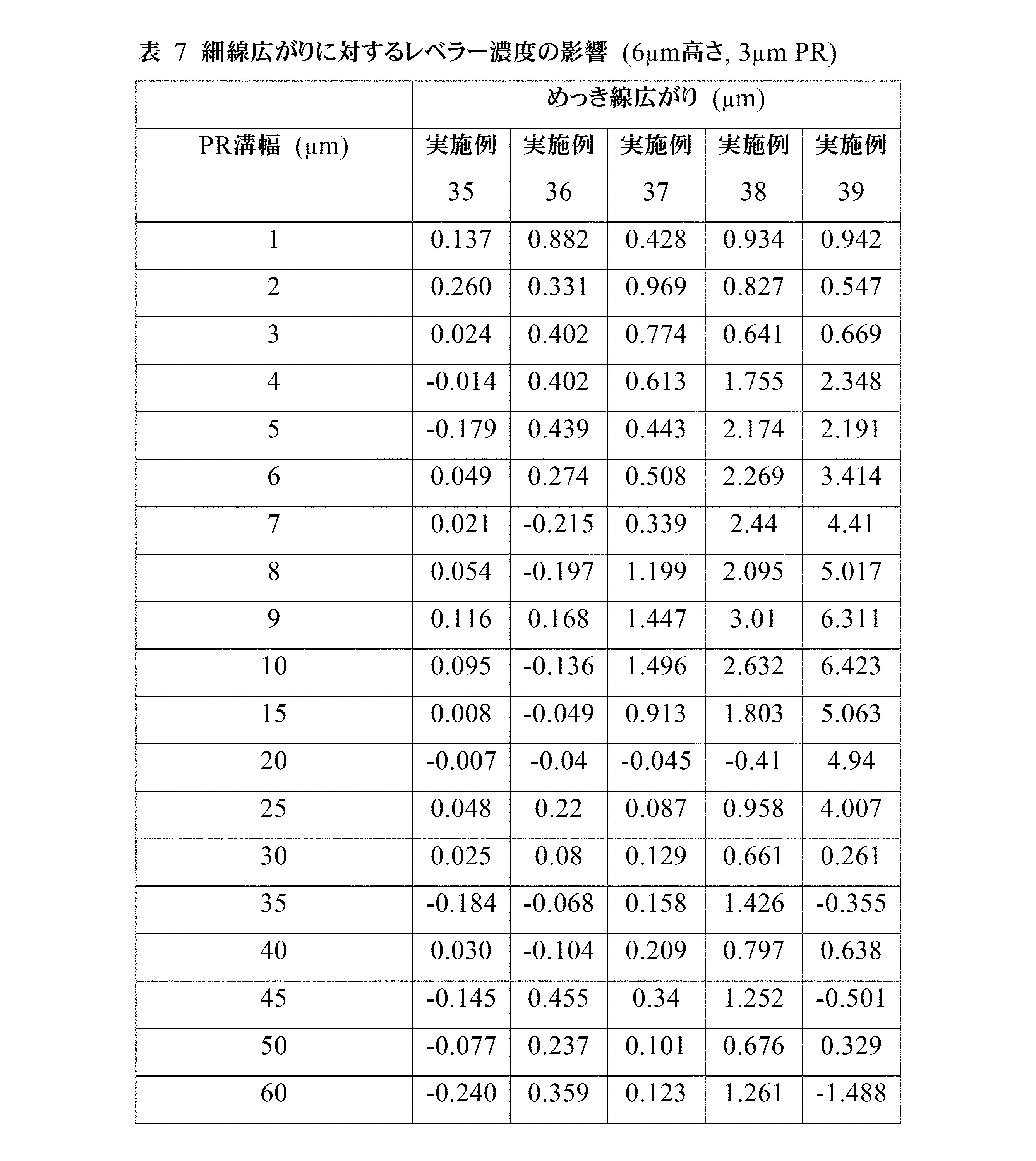
実施例35~39
異なるレベラー濃度での1~60μm幅特徴パターンにおける特徴広がりの制御
20nmのTi接着層及び200nmの導電性Cuシードでコートされたシリコンウェハーを、3μmの厚さのPR層と積層した。幅が1~60μmの範囲の一連の溝を含有するために細線パターンをPR層上に構築した。これらの溝を、次いで、レベラー添加剤の濃度が異なる5つの異なるめっき槽調合物を使用して6μmのターゲット高さまでめっきした:
50g/LのCu(II)イオン
100g/LのH2SO4
50ppmの塩化物イオン
40ppmのビス-ナトリウム-スルホプロピル-ジスルフィド
2g/Lのスルホン化末端基のリバースTetronic、MW 4,800
実施例35:0.1ppmのブチルジグリシジルエーテル、イミダゾール及びフェニルイミダゾールの反応生成物
実施例36:1ppmのブチルジグリシジルエーテル、イミダゾール及びフェニルイミダゾールの反応生成物
実施例37:2ppmのブチルジグリシジルエーテル、イミダゾール及びフェニルイミダゾールの反応生成物
実施例38:5ppmのブチルジグリシジルエーテル、イミダゾール及びフェニルイミダゾールの反応生成物
実施例39:10ppmのブチルジグリシジルエーテル、イミダゾール及びフェニルイミダゾールの反応生成物
各サンプルを、めっき前にDI水でリンスした。全ての場合に、定電流めっきを、50rpmのカソード回転速度で、2ASDで実施した。めっき後に、PRを、PR剥離剤浴中で除去して細線のパターンをもたらした。サンプルを、次いで、シードエッチ液に曝露して、PRによって保護されていた残存導電性シードを除去した。最後に、レーザー表面形状測定装置によってめっき線の幅を測定した。
Examples 35-39
Controlling Feature Spread in 1-60 μm Width Feature Patterns at Different Leveler Concentrations A 20 nm Ti adhesive layer and a silicon wafer coated with a 200 nm conductive Cu seed were laminated with a 3 μm thick PR layer. A fine line pattern was constructed on the PR layer to contain a series of grooves with a width in the range of 1-60 μm. These grooves were then plated to a target height of 6 μm using 5 different plating tank formulations with different levels of leveler additives:
50 g / L Cu (II) ion 100 g / L H 2 SO 4
50
Example 35: Reaction product of 0.1 ppm butyl diglycidyl ether, imidazole and phenyl imidazole Example 36: Reaction product of butyl diglycidyl ether, imidazole and phenyl imidazole at 1 ppm Example 37: 2 ppm butyl diglycidyl ether , Reaction product of imidazole and phenyl imidazole Example 38: Reaction product of butyl diglycidyl ether, imidazole and phenyl imidazole at 5 ppm Example 39: Reaction product of butyl diglycidyl ether, imidazole and phenyl imidazole at 10 ppm Each sample , Rinse with DI water before plating. In all cases, constant current plating was performed at 2 ASD at a cathode speed of 50 rpm. After plating, PR was removed in a PR stripping agent bath to give a fine line pattern. The sample was then exposed to a seed etchant to remove residual conductive seeds protected by PR. Finally, the width of the plated wire was measured by a laser surface shape measuring device.
レベラー添加剤の濃度が低下したときに異方性めっきが最も目立ったことを示す結果を表7に開示する。めっき線広がりを最小限にするという観点からの最良の結果は、レベラー濃度が1ppm以下である場合に得られた。 Table 7 discloses the results showing that the anisotropic plating was most noticeable when the concentration of the leveler additive decreased. The best results from the viewpoint of minimizing the spread of the plated wire were obtained when the leveler concentration was 1 ppm or less.
実施例40~実施例45.界面前処理及び異なるサプレッサー添加剤での1~60μm幅特徴パターンにおける特徴広がりの制御
20nmのTi接着層及び200nmの導電性Cuシードでコートされたシリコンウェハーを、3μmの厚さのPR層と積層した。幅が1~100μmの範囲の一連の溝を包含するために細線パターンをPR層上に構築した。これらの溝を、次いで、サプレッサー添加剤が異なる6つの異なるめっき槽調合物を使用して4.5μmのターゲット高さまでめっきした。
50g/LのCu(II)イオン
100g/LのH2SO4
50ppmの塩化物イオン
2g/Lのサプレッサー添加剤
実施例40:ブロックEO-PO MW 1,100
実施例41:ブロックEO-PO MW 1,950
実施例42:リバースTetronic MW 5,300
実施例43:スルホン化末端基のリバースTetronic、MW 4,800
実施例44:ランダムEO/PO MW 1,100
実施例45:リバースTetronic MW 7,250
各サンプルを、めっき前に先ずpH 0.7かpH 5.5かのどちらかの水中の4g/LのMESの溶液に浸漬し、次いでDI水でリンスした。全ての場合に、電気めっきを、50rpmのカソード回転速度で、2ASDで実施した。めっき後に、PRを、PR剥離剤浴中で除去して細線のパターンをもたらした。サンプルを、次いで、Cu及びTiエッチ液に曝露して、PRによって保護されていた残存導電性シードを除去した。最後に、レーザー表面形状測定装置によってめっき線の幅を測定した。
Examples 40 to 45. Control of feature spread in 1-60 μm wide feature patterns with interfacial pretreatment and different suppressor additives A 20 nm Ti adhesive layer and a 200 nm conductive Cu seed coated silicon wafer are laminated with a 3 μm thick PR layer. did. A fine line pattern was constructed on the PR layer to include a series of grooves with a width in the range of 1-100 μm. These grooves were then plated to a target height of 4.5 μm using 6 different plating tank formulations with different suppressor additives.
50 g / L Cu (II) ion 100 g / L H 2 SO 4
50 ppm Chloride Ion 2 g / L Suppressor Additive Example 40: Block EO-PO MW 1,100
Example 41: Block EO-PO MW 1,950
Example 42: Reverse Tetronic MW 5,300
Example 43: Reverse Tetronic, MW 4,800 of sulfonated end groups
Example 44: Random EO / PO MW 1,100
Example 45: Reverse Tetronic MW 7,250
Each sample was first immersed in a solution of 4 g / L MES in either pH 0.7 or pH 5.5 water prior to plating and then rinsed with DI water. In all cases, electroplating was performed at 2 ASD at a cathode speed of 50 rpm. After plating, PR was removed in a PR stripping agent bath to give a fine line pattern. The sample was then exposed to Cu and Ti etchant to remove residual conductive seeds protected by PR. Finally, the width of the plated wire was measured by a laser surface shape measuring device.
各サンプルを、めっき前に先ずpH 0.7かpH 5.5かのどちらかの水中の4g/LのMESの溶液に浸漬し、次いでDI水でリンスした。全ての場合に、電気めっきを、50rpmのカソード回転速度で、2ASDで実施した。めっき後に、PRを、PR剥離剤浴中で除去して細線のパターンをもたらした。サンプルを、次いで、Cu及びTiエッチ液に曝露して、PRによって保護されていた残存導電性シードを除去した。最後に、レーザー表面形状測定装置によってめっき線の幅を測定した。 Each sample was first immersed in a solution of 4 g / L MES in either pH 0.7 or pH 5.5 water prior to plating and then rinsed with DI water. In all cases, electroplating was performed at 2 ASD at a cathode speed of 50 rpm. After plating, PR was removed in a PR stripping agent bath to give a fine line pattern. The sample was then exposed to Cu and Ti etchant to remove residual conductive seeds protected by PR. Finally, the width of the plated wire was measured by a laser surface shape measuring device.
結果を、全てのサプレッサーの異方性めっきキャラクターをシード活性化が改善したことを示す表8~9に概要を示す。しかしながら、同じパターンは、シード活性化を含まない、実施例35~39において見いだされた。リバースTetronic型サプレッサーが線広がりを最小限にするのに最も有効であり、且つ、リバースTetronic末端鎖のスルホン化が最も目立った異方性めっき挙動をもたらした。 The results are outlined in Tables 8-9 showing that seed activation improved the anisotropic plating character of all suppressors. However, the same pattern was found in Examples 35-39, which did not include seed activation. The reverse Tetronic suppressor was most effective in minimizing line spread, and the sulfonation of the reverse Tetronic end chain resulted in the most noticeable anisotropic plating behavior.
各サンプルを、めっき前に先ずpH 0.7かpH 5.5かのどちらかの水中の4g/LのMESの溶液に浸漬し、次いでDI水でリンスした。全ての場合に、電気めっきを、50rpmのカソード回転速度で、2ASDで実施した。めっき後に、PRを、PR剥離剤浴中で除去して細線のパターンをもたらした。サンプルを、次いで、Cu及びTiエッチ液に曝露して、PRによって保護されていた残存導電性シードを除去した。最後に、レーザー表面形状測定装置によってめっき線の幅を測定した。 Each sample was first immersed in a solution of 4 g / L MES in either pH 0.7 or pH 5.5 water prior to plating and then rinsed with DI water. In all cases, electroplating was performed at 2 ASD at a cathode speed of 50 rpm. After plating, PR was removed in a PR stripping agent bath to give a fine line pattern. The sample was then exposed to Cu and Ti etchant to remove residual conductive seeds protected by PR. Finally, the width of the plated wire was measured by a laser surface shape measuring device.
結果を、全てのサプレッサーの異方性めっきキャラクターをシード活性化が改善することを示す表8~9に示す。しかしながら、シード活性化を含まない、実施例35~39において見いだされた同じパターンが、ここでもまた見いだされた。すなわち、リバースTetronic型サプレッサーが線広がりを最小限にするのに最も有効であり、且つ、リバースTetronic末端鎖のスルホン化が最も目立った異方性めっき挙動をもたらした。 The results are shown in Tables 8-9 showing that seed activation improves the anisotropic plating character of all suppressors. However, the same pattern found in Examples 35-39, without seed activation, was also found here. That is, the reverse Tetronic suppressor was most effective in minimizing line spread, and the sulfonation of the reverse Tetronic end chain resulted in the most noticeable anisotropic plating behavior.
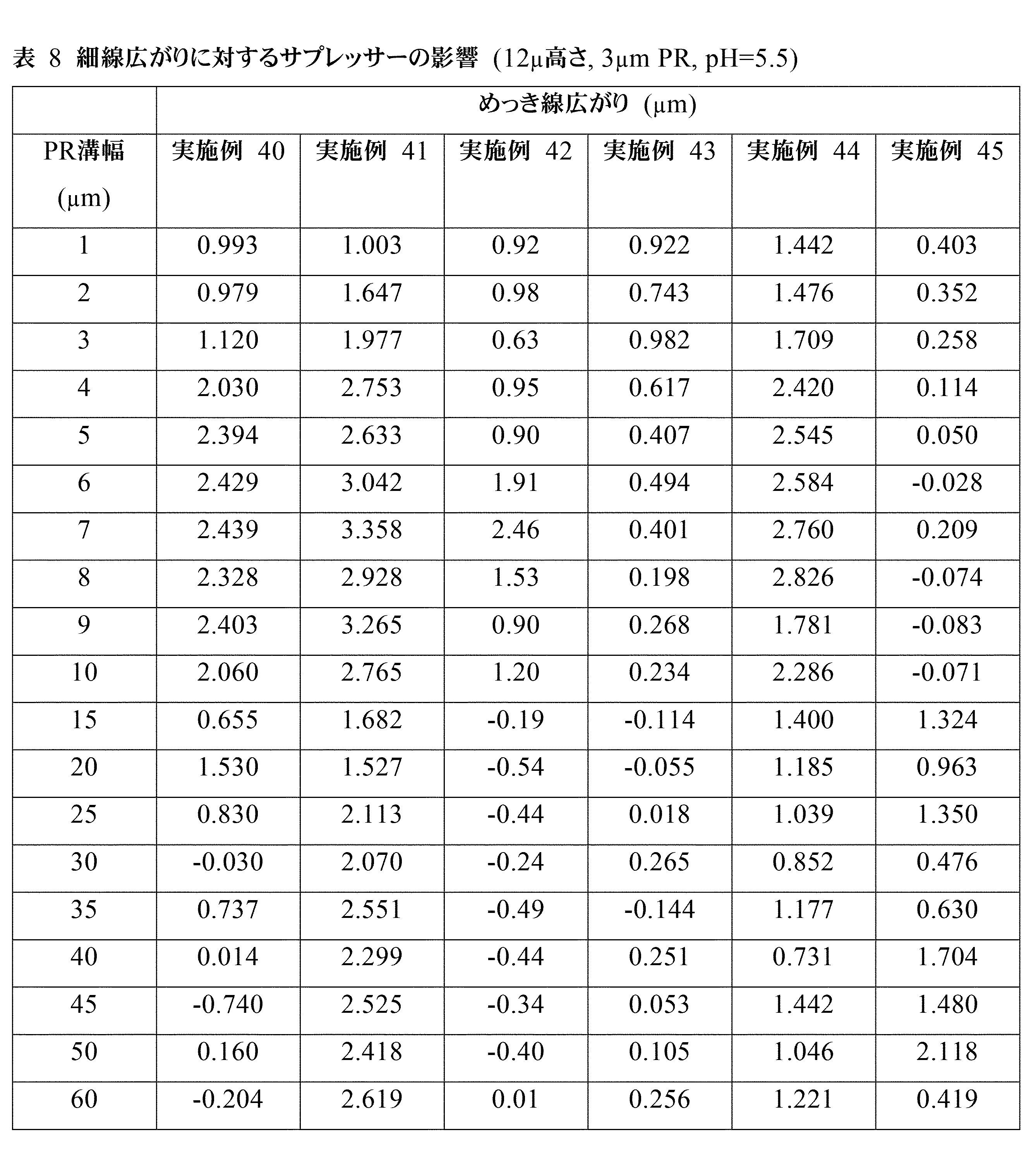
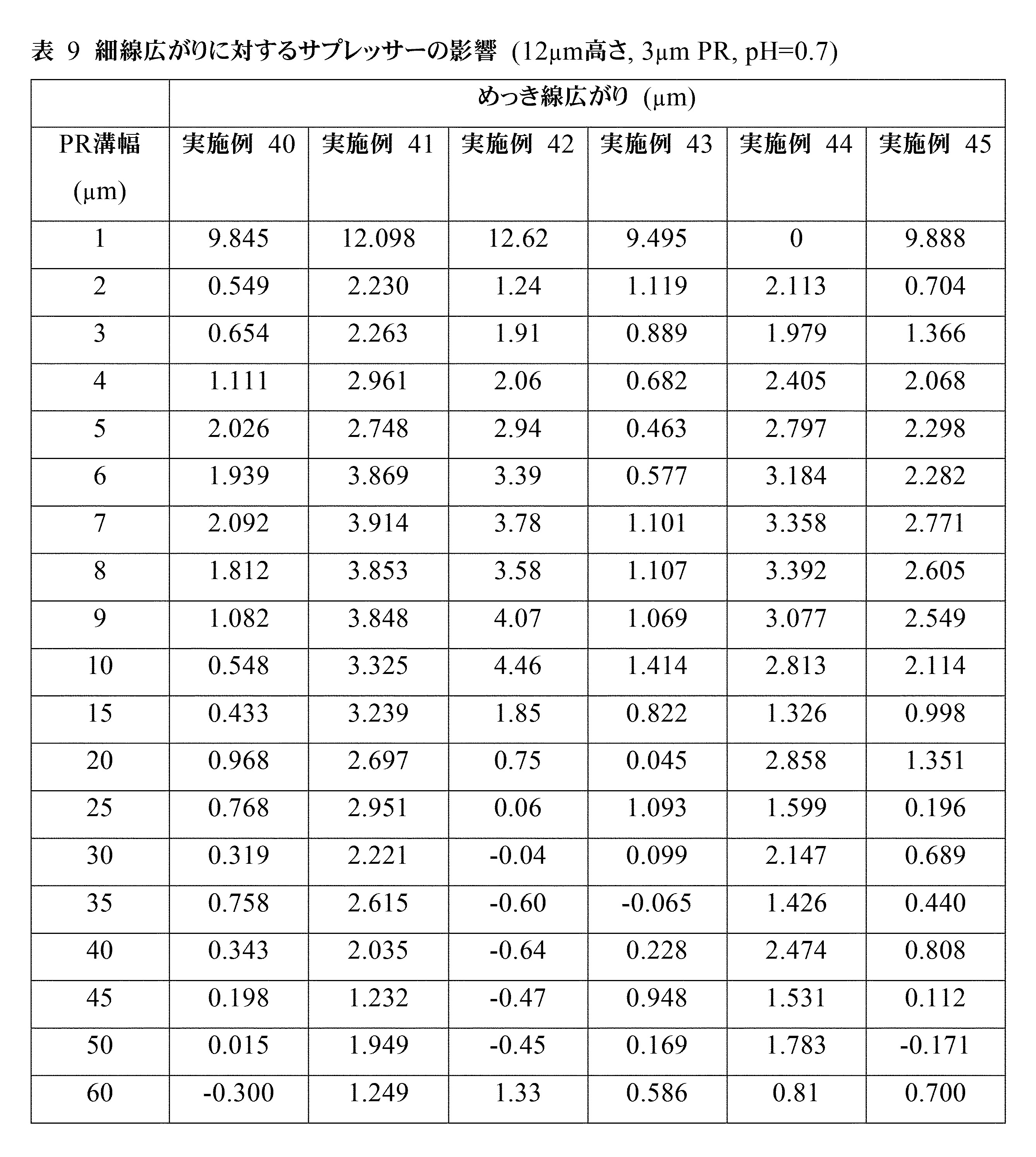
実施例46~48
促進剤及び湿潤剤を含んだシード活性化溶液
同じレベルにされた異方性めっき成長を促進するために湿潤剤を活性化溶液中に含める影響を、線幅が変わる3つの異なる細線パターンに関してテストした。20nmのTi接着層及び200nmの導電性Cuシードでコートされたシリコンウェハーを、3μmの厚さのPR層と積層した。幅が7、20又は100μmの溝を包含するために細線パターンをPR層上に構築した。各パターン中の溝を、次いで、めっき槽1、めっき槽2又はめっき槽3を使用して銅電気めっきによって満たした。サンプルを、めっき前に先ず、水中の4g/LのMES及び1g/LのTN-747湿潤剤のpH 0.7の溶液中に浸漬し、次いでDI水でリンスした。7μmの細線パターンを、9μm(3×PR高さ)の線高さまでめっきし;20μmの細線パターンを、9μm(3×PR高さ)の線高さまでめっきし;100μmの細線パターンを、36μm(12×PR高さ)の線高さまでめっきした。電気めっきを、50rpmのカソード回転速度で、2ASDで実施した。めっき後に、PRを、PR剥離剤浴中で除去して細線のパターンをもたらした。サンプルを、次いで、Cu及びTiエッチ液に曝露して、PRによって保護されていた残存導電性シードを除去した。レーザー表面形状測定装置を用いて孤立Cu細線の幅を測定した。表10にまとめられた、結果は、より短いPR溝の幅を越えて線厚さが増加するのを異方性めっき槽3が防ぐことを示した。等方性めっき槽1は、PR溝の高さの上方にめっきされる場合にめっき線が融合するのを防止せず、したがって細線パターンを破壊した。中間の異方性挙動を有する、めっき槽2は、細線幅の小さい増加を示した。線融合が起こった。前処理液中の湿潤剤は、露出シードの全ての部分が促進剤成分と相互作用するのを可能にすることによって同じレベルにされためっきを確実にした。全体として、データは、めっき異方性の程度を制御するためにめっき槽調合物を調整できることを示した。
Examples 46-48
Seed activation solution containing accelerator and wetting agent The effect of including the wetting agent in the activation solution to promote anisotropic plating growth at the same level was tested for three different fine line patterns with varying line widths. did. A silicon wafer coated with a 20 nm Ti adhesive layer and a 200 nm conductive Cu seed was laminated with a 3 μm thick PR layer. A fine line pattern was constructed on the PR layer to include grooves with a width of 7, 20 or 100 μm. The grooves in each pattern were then filled by copper electroplating using
実施例49~56.
めっき特徴形状に対する活性化剤pHの影響
細線フィル形状の制御を、前処理液のpHを調整することによって研究した。上記の実施例1~2において使用された同じ細線パターンを、電気めっき前に0.7、3、4、5.5、8、9、13又は14のpHの4g/LのMES水溶液で処理し、DI水でリンスした。サンプルを、次いで、5μm(1.66×PR高さ)のターゲット高さまでめっき槽3で電気めっきした。全ての場合に、電気めっきを、50rpmのカソード回転速度で、2ASDで実施した。めっき後に、PRを、PR剥離剤浴中で除去して細線のパターンをもたらした。サンプルを、次いで、Cu及びTiエッチ液に曝露して、PRによって保護されていた残存導電性シードを除去した。レーザー表面形状測定装置を用いて孤立Cu細線の幅を測定した。表11にまとめられた、結果は、前処理液のpHにかかわらず同じレベルにされためっきが可能であることを示した。しかしながら、細線のフィル形状は、著しく変化する;すなわち、高いpHは、皿形めっき形状を促進し、一方、低いpHは、ややドーム形形状を促進した。より中間のpH(pH=4~8)は、一層目立ったドーム形形状をもたらす。下記のデータが示すように、中間pH範囲は、異方性めっき槽調合物で所望のフィル形状にアクセスするために有利ではない。代わりに、中間範囲外のpH範囲を維持することによって、異方性めっきは、ドーミングプロファイルを減らす又は皿形プロファイルを誘導するためにさらに調整することができる。
Examples 49-56.
Effect of activator pH on plating feature shape Control of fine wire fill shape was studied by adjusting the pH of the pretreatment solution. The same fine wire pattern used in Examples 1 and 2 above is treated with a 4 g / L MES aqueous solution at a pH of 0.7, 3, 4, 5.5, 8, 9, 13 or 14 prior to electroplating. Then rinsed with DI water. The sample was then electroplated in the plating tank 3 to a target height of 5 μm (1.66 × PR height). In all cases, electroplating was performed at 2 ASD at a cathode speed of 50 rpm. After plating, PR was removed in a PR stripping agent bath to give a fine line pattern. The sample was then exposed to Cu and Ti etchant to remove residual conductive seeds protected by PR. The width of the isolated Cu thin wire was measured using a laser surface shape measuring device. The results summarized in Table 11 show that plating at the same level is possible regardless of the pH of the pretreatment solution. However, the fill shape of the fine wire varies significantly; that is, high pH promotes the dish-shaped plating shape, while low pH promotes the slightly dome-shaped shape. A more intermediate pH (pH = 4-8) results in a more prominent dome shape. As the data below show, the intermediate pH range is not advantageous for accessing the desired fill shape in the anisotropic plating tank formulation. Alternatively, by maintaining a pH range outside the midrange, anisotropic plating can be further adjusted to reduce the doming profile or induce a dish profile.
実施例57~59
活性化後に及び電解めっき前にPR層を除去する場合の異方性めっき
めっき中にパターン化層の不在下でさえも特徴解像度を持続する本明細書で記載される異方性めっき方法論の能力を研究した。そうするために、PR層なしの対照等方性ランに対してPR層あり及びなしのめっき異方性性能をテストし比較するための3つのめっきシナリオを検討した。実施例3~6からの同じパターン化基材を使用した。実施例57サンプルは、4g/LのMES水溶液で前処理し、DI水でリンスし、めっき前に1:1のジメチルスルホキシド-γ-ブチロラクトン混合物を使用してPR層を除去した。実施例58サンプルは、4g/LのMES水溶液で前処理し、DI水でリンスするのみであった。実施例59サンプルは、DI水で前処理したのみであった。実施例57~58サンプルをめっき槽3でめっきし、実施例59サンプルをめっき槽1でめっきした。全ての3つのサンプルを、50rpmのカソード回転速度及び5μmのめっきターゲット高さで、2ASDでめっきした。めっき後に、PRを、Shipley BPRTM PR剥離剤浴中で除去して細線のパターンをもたらした。サンプルを、次いで、シードエッチ液に曝露して、PRによって保護されていた残存導電性シードを除去した。レーザー表面形状測定装置を用いて孤立Cu細線の幅及び高さを測定した。表12にまとめられた、結果は、実施例57~58サンプルでは著しい線融合が防がれ、ここで、めっき中にパターン化PR層の不在下でさえも異方性めっきが起こることを示した。その一方で、実施例59サンプルは、全ての細線幅で著しい線融合を示した。表13に示されるように全てのサンプルは、特徴幅範囲にわたってめっき高さの良好なレベリングを示した。
Examples 57-59
Anisotropic plating when removing the PR layer after activation and before electroplating The ability of the anisotropic plating methodologies described herein to sustain feature resolution even in the absence of patterned layers during plating. Was studied. To do so, three plating scenarios were considered to test and compare the plating anisotropic performance with and without the PR layer for control isotropic runs without the PR layer. The same patterned substrate from Examples 3-6 was used. The 57 samples of Example 57 were pretreated with 4 g / L aqueous MES solution, rinsed with DI water, and the PR layer was removed using a 1: 1 dimethyl sulfoxide-γ-butyrolactone mixture prior to plating. The 58 samples of Example 58 were only pretreated with a 4 g / L MES aqueous solution and rinsed with DI water. Example 59 samples were only pretreated with DI water. Examples 57 to 58 samples were plated in the plating tank 3, and Examples 59 samples were plated in the
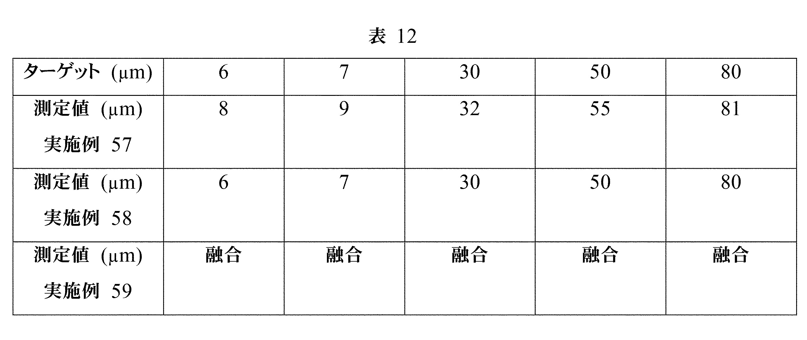
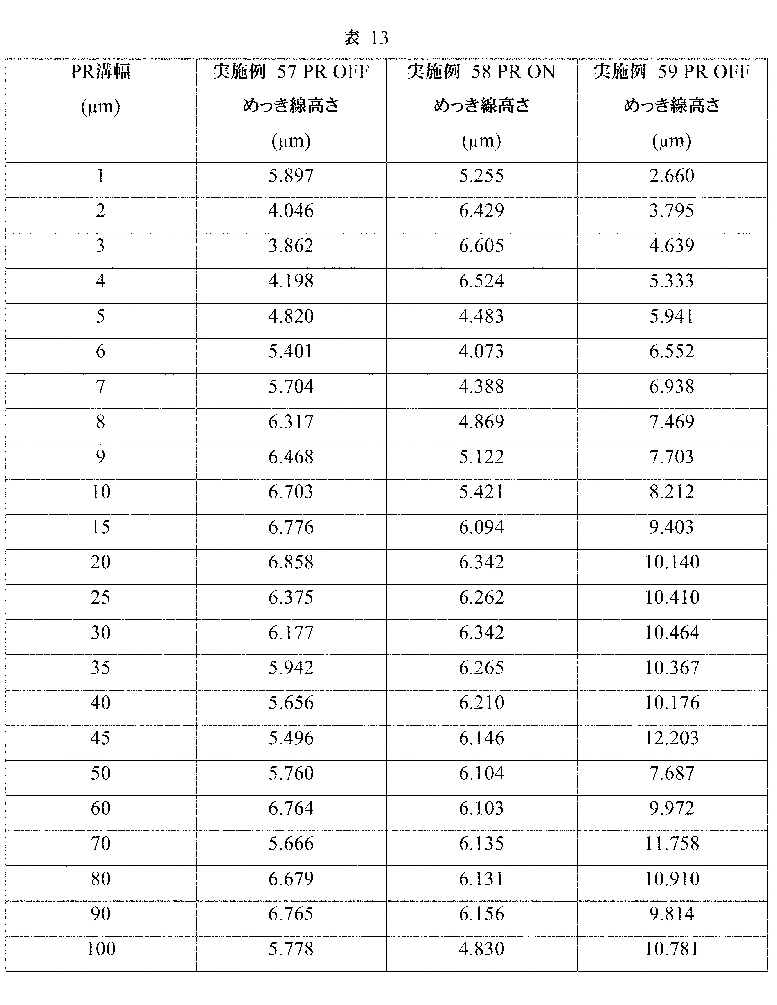
20 誘電体基材
22 銅シード層
24 画像形成フォトレジスト
26 等方性銅線
28 凹部
30 誘電体基材
32 銅シード層
34 画像形成フォトレジスト
36 異方性銅ピラー
38 凹部
40 基材
42 銅シード層
44 画像形成フォトレジスト
46 開口部
48 露出シード層
50 処理シード層
52 銅線
20
Claims (10)
b)任意選択的に、硫黄含有促進剤を含む水性処理液を前記シード層に選択的に適用する工程であって、前記水性処理液のpHが3未満、又は9超である工程と;
c)銅イオンの供給源、促進剤、酸、塩化物の供給源、作用電極上の銅電気めっき組成物のボルタンモグラムのカソード波におけるα-ピーク曲線を発生させるサプレッサー、及びレベラーを含む銅電気めっき組成物を提供する工程であって、前記レベラーがイミダゾール及びブチルジグリシジルエーテルの反応生成物のコポリマー又はイミダゾール及びフェニルイミダゾールの反応生成物のコポリマーである工程と;
d)前記シード層を含む前記基材を前記銅電気めっき組成物と接触させる工程と;
e)前記基材の前記シード層上に銅を非等方的に電気めっきする工程と
を含む方法。 a) A step of providing a substrate containing a seed layer;
b) Optionally, a step of selectively applying an aqueous treatment liquid containing a sulfur-containing accelerator to the seed layer, wherein the pH of the aqueous treatment liquid is less than 3 or more than 9.
c) Copper ion sources, accelerators, acids, chloride sources, copper electroplating containing a suppressor to generate an α-peak curve in the cathode wave of the voltanmogram of the copper electroplating composition on the working electrode, and a leveler. The step of providing the composition, wherein the leveler is a copolymer of a reaction product of imidazole and butyl diglycidyl ether or a copolymer of a reaction product of imidazole and phenyl imidazole;
d) A step of bringing the base material containing the seed layer into contact with the copper electroplating composition;
e) A method comprising a step of isotropically electroplating copper on the seed layer of the substrate.
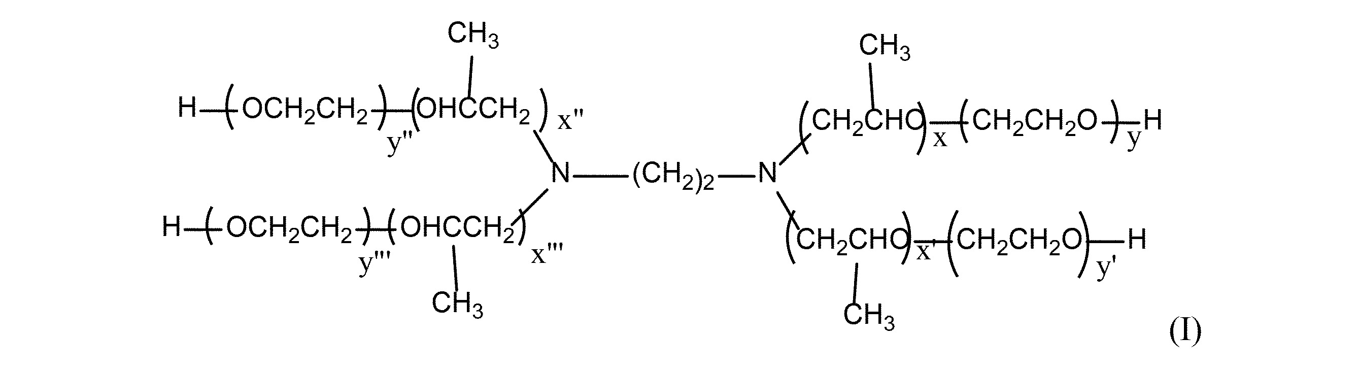
を有する、請求項5に記載の方法。 The diamine core EO / PO block copolymer has the formula:
5. The method of claim 5.
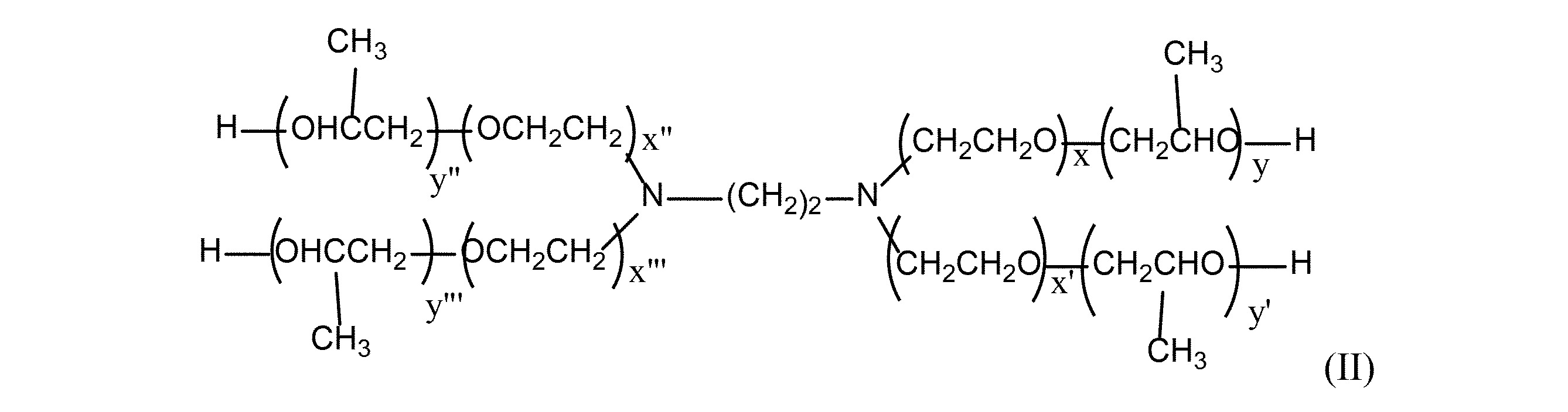
を有する、請求項5に記載の方法。 The diamine core EO / PO block copolymer has the formula:
5. The method of claim 5.

を有する、請求項5に記載の方法。 The diamine core EO / PO block copolymer has the formula:
5. The method of claim 5.
b)前記シード層をフォトレジストでコートする工程と;
c)前記フォトレジストを画像形成して前記基材上にパターンを形成し、シード層を選択的に露出させる工程と;
d)任意選択的に、硫黄含有促進剤を含む水性処理液を前記露出シード層に適用する工程であって、前記水性処理液が3未満のpH、又は9超のpHを有する工程と;
e)銅イオンの供給源、促進剤、酸、塩化物の供給源、作用電極上の銅電気めっき組成物のボルタンモグラムのカソード波におけるα-ピーク曲線を発生させるサプレッサー、及びレベラーを含む銅電気めっき組成物を提供する工程であって、前記レベラーがイミダゾール及びブチルジグリシジルエーテルの反応生成物のコポリマー又はイミダゾール及びフェニルイミダゾールの反応生成物のコポリマーである工程と;
f)前記シード層を含む前記基材を異方性銅電気めっき組成物と接触させる工程と;
g)前記基材の前記シード層上に異方性銅を電気めっきする工程と
を含む方法。 a) A step of providing a substrate containing a seed layer;
b) The step of coating the seed layer with a photoresist;
c) A step of forming an image of the photoresist, forming a pattern on the substrate, and selectively exposing the seed layer;
d) Optionally, a step of applying an aqueous treatment solution containing a sulfur-containing accelerator to the exposed seed layer, wherein the aqueous treatment solution has a pH of less than 3 or a pH of more than 9.
e) Copper ion sources, accelerators, acids, chloride sources, copper electroplating containing a suppressor to generate an α-peak curve in the cathode wave of the voltanmogram of the copper electroplating composition on the working electrode, and a leveler. The step of providing the composition, wherein the leveler is a copolymer of a reaction product of imidazole and butyl diglycidyl ether or a copolymer of a reaction product of imidazole and phenyl imidazole;
f) A step of contacting the base material containing the seed layer with the anisotropic copper electroplating composition;
g) A method comprising a step of electroplating anisotropic copper on the seed layer of the substrate.
It contains copper deposits at least 2 μm above the height of the surrounding photoresist, contains unmatched boundaries oriented at 80-90 ° with respect to the plane of the substrate, and 40-to 40-with respect to the plane of said substrate. Articles containing parallel bicrystal boundaries oriented at 50 °.
Applications Claiming Priority (2)
| Application Number | Priority Date | Filing Date | Title |
|---|---|---|---|
| US202163134348P | 2021-01-06 | 2021-01-06 | |
| US63/134,348 | 2021-01-06 |
Publications (2)
| Publication Number | Publication Date |
|---|---|
| JP2022106295A true JP2022106295A (en) | 2022-07-19 |
| JP7300530B2 JP7300530B2 (en) | 2023-06-29 |
Family
ID=82218556
Family Applications (1)
| Application Number | Title | Priority Date | Filing Date |
|---|---|---|---|
| JP2022000874A Active JP7300530B2 (en) | 2021-01-06 | 2022-01-06 | Improving photoresist resolution capability by anisotropically copper electroplating |
Country Status (4)
| Country | Link |
|---|---|
| US (1) | US20220213610A1 (en) |
| JP (1) | JP7300530B2 (en) |
| KR (1) | KR102667535B1 (en) |
| CN (1) | CN114717615B (en) |
Families Citing this family (1)
| Publication number | Priority date | Publication date | Assignee | Title |
|---|---|---|---|---|
| US12557666B2 (en) * | 2022-11-28 | 2026-02-17 | Taiwan Semiconductor Manufacturing Company, Ltd. | Method of manufacturing conductive structure, method of manufacturing redistribution circuit structure and method of manufacturing semiconductor package |
Citations (7)
| Publication number | Priority date | Publication date | Assignee | Title |
|---|---|---|---|---|
| JP2008519908A (en) * | 2004-11-12 | 2008-06-12 | エントン インコーポレイテッド | Copper electrical deposition method in microelectronics |
| JP2012127003A (en) * | 2010-12-15 | 2012-07-05 | Rohm & Haas Electronic Materials Llc | Method of electroplating uniform copper layer |
| JP2013044035A (en) * | 2011-08-25 | 2013-03-04 | Ishihara Chem Co Ltd | Method of filling copper, and electronic component using the same |
| JP2014177704A (en) * | 2013-03-14 | 2014-09-25 | Rohm & Haas Electronic Materials Llc | Through hole filling method |
| JP2019085645A (en) * | 2017-11-08 | 2019-06-06 | ローム アンド ハース エレクトロニック マテリアルズ エルエルシーRohm and Haas Electronic Materials LLC | Copper electroplating compositions and methods of electroplating substrates with copper |
| JP2019085647A (en) * | 2017-11-08 | 2019-06-06 | ローム アンド ハース エレクトロニック マテリアルズ エルエルシーRohm and Haas Electronic Materials LLC | Electroplated copper |
| JP2020513475A (en) * | 2016-11-18 | 2020-05-14 | ハッチンソン テクノロジー インコーポレイテッドHutchinson Technology Incorporated | High aspect ratio electroplating structure and anisotropic electroplating process |
Family Cites Families (7)
| Publication number | Priority date | Publication date | Assignee | Title |
|---|---|---|---|---|
| JP4862508B2 (en) * | 2006-06-12 | 2012-01-25 | 日立電線株式会社 | Conductor pattern forming method |
| US8962085B2 (en) * | 2009-06-17 | 2015-02-24 | Novellus Systems, Inc. | Wetting pretreatment for enhanced damascene metal filling |
| WO2016098680A1 (en) * | 2014-12-17 | 2016-06-23 | Dic株式会社 | Primer composition for plating, base to be plated, composite body of insulating base and metal layer, method for producing base to be plated, and method for producing composite body of insulating base and metal layer |
| US10988852B2 (en) * | 2015-10-27 | 2021-04-27 | Rohm And Haas Electronic Materials Llc | Method of electroplating copper into a via on a substrate from an acid copper electroplating bath |
| US10512174B2 (en) * | 2016-02-15 | 2019-12-17 | Rohm And Haas Electronic Materials Llc | Method of filling through-holes to reduce voids and other defects |
| CN109996785B (en) * | 2016-09-22 | 2021-12-28 | 麦克德米德乐思公司 | Copper deposition in wafer level packaging of integrated circuits |
| CN106521573B (en) * | 2016-11-23 | 2019-10-01 | 苏州昕皓新材料科技有限公司 | Prepare the method and its application with the copper electroplating layer of preferred orientation growth structure |
-
2021
- 2021-12-29 US US17/564,810 patent/US20220213610A1/en not_active Abandoned
-
2022
- 2022-01-06 JP JP2022000874A patent/JP7300530B2/en active Active
- 2022-01-06 KR KR1020220001951A patent/KR102667535B1/en active Active
- 2022-01-06 CN CN202210014611.6A patent/CN114717615B/en active Active
Patent Citations (7)
| Publication number | Priority date | Publication date | Assignee | Title |
|---|---|---|---|---|
| JP2008519908A (en) * | 2004-11-12 | 2008-06-12 | エントン インコーポレイテッド | Copper electrical deposition method in microelectronics |
| JP2012127003A (en) * | 2010-12-15 | 2012-07-05 | Rohm & Haas Electronic Materials Llc | Method of electroplating uniform copper layer |
| JP2013044035A (en) * | 2011-08-25 | 2013-03-04 | Ishihara Chem Co Ltd | Method of filling copper, and electronic component using the same |
| JP2014177704A (en) * | 2013-03-14 | 2014-09-25 | Rohm & Haas Electronic Materials Llc | Through hole filling method |
| JP2020513475A (en) * | 2016-11-18 | 2020-05-14 | ハッチンソン テクノロジー インコーポレイテッドHutchinson Technology Incorporated | High aspect ratio electroplating structure and anisotropic electroplating process |
| JP2019085645A (en) * | 2017-11-08 | 2019-06-06 | ローム アンド ハース エレクトロニック マテリアルズ エルエルシーRohm and Haas Electronic Materials LLC | Copper electroplating compositions and methods of electroplating substrates with copper |
| JP2019085647A (en) * | 2017-11-08 | 2019-06-06 | ローム アンド ハース エレクトロニック マテリアルズ エルエルシーRohm and Haas Electronic Materials LLC | Electroplated copper |
Also Published As
| Publication number | Publication date |
|---|---|
| CN114717615A (en) | 2022-07-08 |
| KR102667535B1 (en) | 2024-05-22 |
| US20220213610A1 (en) | 2022-07-07 |
| KR20220099505A (en) | 2022-07-13 |
| JP7300530B2 (en) | 2023-06-29 |
| TW202231932A (en) | 2022-08-16 |
| CN114717615B (en) | 2025-06-24 |
Similar Documents
| Publication | Publication Date | Title |
|---|---|---|
| JP4472157B2 (en) | Via filling method | |
| US6607654B2 (en) | Copper-plating elecrolyte containing polyvinylpyrrolidone and method for forming a copper interconnect | |
| US20080264798A1 (en) | Copper Plating Bath and Plating Method | |
| KR102468093B1 (en) | Method of enhancing copper electroplating | |
| EP3128041B1 (en) | Method of electroplating photoresist defined features from copper electroplating baths containing reaction products of pyridyl alkylamines and bisepoxides | |
| US20080087549A1 (en) | Additive For Copper Plating And Process For Producing Electronic Circiut Substrate Therewith | |
| JP2010242151A (en) | Copper filling method | |
| JP7138108B2 (en) | Copper Electrodeposition Solution and Process for High Aspect Ratio Patterns | |
| EP3128042A1 (en) | Method of electroplating photoresist defined features from copper electroplating baths containing reaction products of imidazole and bisepoxide compounds | |
| CN111058066A (en) | Application of sodium polydithio-ethane sulfonate as accelerator and electroplating solution containing sodium polydithio-ethane sulfonate | |
| JP7300530B2 (en) | Improving photoresist resolution capability by anisotropically copper electroplating | |
| WO2019179897A1 (en) | Process for electrodeposition of cobalt | |
| US10508349B2 (en) | Method of electroplating photoresist defined features from copper electroplating baths containing reaction products of pyrazole compounds and bisepoxides | |
| US11384445B2 (en) | Process for electrodeposition of cobalt | |
| US10329681B2 (en) | Copper-silver dual-component metal electroplating solution and electroplating method for semiconductor wire | |
| KR102913509B1 (en) | Electrolyte containing an accelerator for bottom-up copper electroplating | |
| US20250215598A1 (en) | Leveling agent, composition, and application thereof | |
| HK40122506A (en) | Electrolyte comprising an accelerator agent for bottom-up copper electroplating | |
| HK40122506B (en) | Electrolyte comprising an accelerator agent for bottom-up copper electroplating | |
| TW201910559A (en) | Copper-silver two-component metal plating liquid for semiconductor wires and plating method comprising copper methanesulfonate, silver methanesulfonate, methanesulfonic acid, chloride ions and water |
Legal Events
| Date | Code | Title | Description |
|---|---|---|---|
| A621 | Written request for application examination |
Free format text: JAPANESE INTERMEDIATE CODE: A621 Effective date: 20220207 |
|
| RD02 | Notification of acceptance of power of attorney |
Free format text: JAPANESE INTERMEDIATE CODE: A7422 Effective date: 20220208 |
|
| RD04 | Notification of resignation of power of attorney |
Free format text: JAPANESE INTERMEDIATE CODE: A7424 Effective date: 20220506 |
|
| A977 | Report on retrieval |
Free format text: JAPANESE INTERMEDIATE CODE: A971007 Effective date: 20230117 |
|
| A131 | Notification of reasons for refusal |
Free format text: JAPANESE INTERMEDIATE CODE: A131 Effective date: 20230203 |
|
| A521 | Request for written amendment filed |
Free format text: JAPANESE INTERMEDIATE CODE: A523 Effective date: 20230502 |
|
| TRDD | Decision of grant or rejection written | ||
| A01 | Written decision to grant a patent or to grant a registration (utility model) |
Free format text: JAPANESE INTERMEDIATE CODE: A01 Effective date: 20230526 |
|
| A61 | First payment of annual fees (during grant procedure) |
Free format text: JAPANESE INTERMEDIATE CODE: A61 Effective date: 20230619 |
|
| R150 | Certificate of patent or registration of utility model |
Ref document number: 7300530 Country of ref document: JP Free format text: JAPANESE INTERMEDIATE CODE: R150 |
|
| S533 | Written request for registration of change of name |
Free format text: JAPANESE INTERMEDIATE CODE: R313533 |
|
| R350 | Written notification of registration of transfer |
Free format text: JAPANESE INTERMEDIATE CODE: R350 |