JP2022104835A - Organic semiconductor device, organic el device, photodiode sensor, display device, light emitting device, electronic device, and lighting device - Google Patents
Organic semiconductor device, organic el device, photodiode sensor, display device, light emitting device, electronic device, and lighting device Download PDFInfo
- Publication number
- JP2022104835A JP2022104835A JP2021215428A JP2021215428A JP2022104835A JP 2022104835 A JP2022104835 A JP 2022104835A JP 2021215428 A JP2021215428 A JP 2021215428A JP 2021215428 A JP2021215428 A JP 2021215428A JP 2022104835 A JP2022104835 A JP 2022104835A
- Authority
- JP
- Japan
- Prior art keywords
- layer
- organic
- hole transport
- abbreviation
- light emitting
- Prior art date
- Legal status (The legal status is an assumption and is not a legal conclusion. Google has not performed a legal analysis and makes no representation as to the accuracy of the status listed.)
- Pending
Links
- 239000004065 semiconductor Substances 0.000 title claims abstract description 73
- 230000005525 hole transport Effects 0.000 claims abstract description 254
- 150000002894 organic compounds Chemical class 0.000 claims abstract description 180
- 239000000758 substrate Substances 0.000 claims description 91
- 230000008021 deposition Effects 0.000 claims description 12
- 238000007740 vapor deposition Methods 0.000 abstract description 45
- 239000010410 layer Substances 0.000 description 682
- 238000005401 electroluminescence Methods 0.000 description 231
- 239000010408 film Substances 0.000 description 182
- 239000000463 material Substances 0.000 description 167
- 101100449748 Crithidia fasciculata GSP gene Proteins 0.000 description 98
- 102100032611 Guanine nucleotide-binding protein G(s) subunit alpha isoforms short Human genes 0.000 description 98
- 101100162404 Homo sapiens GNAS gene Proteins 0.000 description 98
- -1 aromatic amine compound Chemical class 0.000 description 87
- 238000000034 method Methods 0.000 description 86
- 239000000126 substance Substances 0.000 description 84
- YXFVVABEGXRONW-UHFFFAOYSA-N Toluene Chemical compound CC1=CC=CC=C1 YXFVVABEGXRONW-UHFFFAOYSA-N 0.000 description 81
- 238000002347 injection Methods 0.000 description 68
- 239000007924 injection Substances 0.000 description 68
- 229910052757 nitrogen Inorganic materials 0.000 description 66
- 238000010586 diagram Methods 0.000 description 59
- 230000000052 comparative effect Effects 0.000 description 46
- 125000001997 phenyl group Chemical group [H]C1=C([H])C([H])=C(*)C([H])=C1[H] 0.000 description 41
- LFQSCWFLJHTTHZ-UHFFFAOYSA-N Ethanol Chemical compound CCO LFQSCWFLJHTTHZ-UHFFFAOYSA-N 0.000 description 38
- 230000015572 biosynthetic process Effects 0.000 description 38
- 238000003786 synthesis reaction Methods 0.000 description 37
- 150000001875 compounds Chemical class 0.000 description 36
- 239000000243 solution Substances 0.000 description 35
- 239000007787 solid Substances 0.000 description 34
- 239000010409 thin film Substances 0.000 description 30
- ODHXBMXNKOYIBV-UHFFFAOYSA-N triphenylamine Chemical compound C1=CC=CC=C1N(C=1C=CC=CC=1)C1=CC=CC=C1 ODHXBMXNKOYIBV-UHFFFAOYSA-N 0.000 description 29
- 238000004770 highest occupied molecular orbital Methods 0.000 description 27
- 229910052751 metal Inorganic materials 0.000 description 26
- 239000002184 metal Substances 0.000 description 26
- 238000000295 emission spectrum Methods 0.000 description 25
- 238000007789 sealing Methods 0.000 description 25
- 238000004519 manufacturing process Methods 0.000 description 24
- IJGRMHOSHXDMSA-UHFFFAOYSA-N Atomic nitrogen Chemical compound N#N IJGRMHOSHXDMSA-UHFFFAOYSA-N 0.000 description 23
- 238000005192 partition Methods 0.000 description 23
- 239000003566 sealing material Substances 0.000 description 21
- 239000002131 composite material Substances 0.000 description 20
- 239000000203 mixture Substances 0.000 description 20
- 230000005284 excitation Effects 0.000 description 19
- 239000011521 glass Substances 0.000 description 19
- MILUBEOXRNEUHS-UHFFFAOYSA-N iridium(3+) Chemical compound [Ir+3] MILUBEOXRNEUHS-UHFFFAOYSA-N 0.000 description 19
- QJGQUHMNIGDVPM-UHFFFAOYSA-N nitrogen group Chemical group [N] QJGQUHMNIGDVPM-UHFFFAOYSA-N 0.000 description 19
- XLYOFNOQVPJJNP-UHFFFAOYSA-N water Substances O XLYOFNOQVPJJNP-UHFFFAOYSA-N 0.000 description 19
- 239000011159 matrix material Substances 0.000 description 18
- 230000010287 polarization Effects 0.000 description 17
- 229910052782 aluminium Inorganic materials 0.000 description 16
- 125000001072 heteroaryl group Chemical group 0.000 description 16
- XLOMVQKBTHCTTD-UHFFFAOYSA-N Zinc monoxide Chemical compound [Zn]=O XLOMVQKBTHCTTD-UHFFFAOYSA-N 0.000 description 15
- 238000010438 heat treatment Methods 0.000 description 15
- 238000001259 photo etching Methods 0.000 description 15
- VYPSYNLAJGMNEJ-UHFFFAOYSA-N Silicium dioxide Chemical compound O=[Si]=O VYPSYNLAJGMNEJ-UHFFFAOYSA-N 0.000 description 13
- 239000007983 Tris buffer Substances 0.000 description 13
- CUJRVFIICFDLGR-UHFFFAOYSA-N acetylacetonate Chemical compound CC(=O)[CH-]C(C)=O CUJRVFIICFDLGR-UHFFFAOYSA-N 0.000 description 13
- XAGFODPZIPBFFR-UHFFFAOYSA-N aluminium Chemical compound [Al] XAGFODPZIPBFFR-UHFFFAOYSA-N 0.000 description 13
- CSNNHWWHGAXBCP-UHFFFAOYSA-L Magnesium sulfate Chemical compound [Mg+2].[O-][S+2]([O-])([O-])[O-] CSNNHWWHGAXBCP-UHFFFAOYSA-L 0.000 description 12
- 150000004982 aromatic amines Chemical class 0.000 description 12
- 125000003118 aryl group Chemical group 0.000 description 12
- 125000000319 biphenyl-4-yl group Chemical group [H]C1=C([H])C([H])=C([H])C([H])=C1C1=C([H])C([H])=C([*])C([H])=C1[H] 0.000 description 12
- 238000000151 deposition Methods 0.000 description 12
- 229910052741 iridium Inorganic materials 0.000 description 12
- GKOZUEZYRPOHIO-UHFFFAOYSA-N iridium atom Chemical compound [Ir] GKOZUEZYRPOHIO-UHFFFAOYSA-N 0.000 description 12
- VLKZOEOYAKHREP-UHFFFAOYSA-N n-Hexane Chemical compound CCCCCC VLKZOEOYAKHREP-UHFFFAOYSA-N 0.000 description 12
- 230000001681 protective effect Effects 0.000 description 12
- 238000010898 silica gel chromatography Methods 0.000 description 12
- MFRIHAYPQRLWNB-UHFFFAOYSA-N sodium tert-butoxide Chemical compound [Na+].CC(C)(C)[O-] MFRIHAYPQRLWNB-UHFFFAOYSA-N 0.000 description 12
- 230000001052 transient effect Effects 0.000 description 12
- 238000005160 1H NMR spectroscopy Methods 0.000 description 11
- JUJWROOIHBZHMG-UHFFFAOYSA-N Pyridine Chemical group C1=CC=NC=C1 JUJWROOIHBZHMG-UHFFFAOYSA-N 0.000 description 11
- 150000001412 amines Chemical class 0.000 description 11
- 125000000609 carbazolyl group Chemical group C1(=CC=CC=2C3=CC=CC=C3NC12)* 0.000 description 11
- 238000004140 cleaning Methods 0.000 description 11
- AMGQUBHHOARCQH-UHFFFAOYSA-N indium;oxotin Chemical compound [In].[Sn]=O AMGQUBHHOARCQH-UHFFFAOYSA-N 0.000 description 11
- 229910052814 silicon oxide Inorganic materials 0.000 description 11
- UJOBWOGCFQCDNV-UHFFFAOYSA-N 9H-carbazole Chemical compound C1=CC=C2C3=CC=CC=C3NC2=C1 UJOBWOGCFQCDNV-UHFFFAOYSA-N 0.000 description 10
- 150000001340 alkali metals Chemical class 0.000 description 10
- GQVWHWAWLPCBHB-UHFFFAOYSA-L beryllium;benzo[h]quinolin-10-olate Chemical compound [Be+2].C1=CC=NC2=C3C([O-])=CC=CC3=CC=C21.C1=CC=NC2=C3C([O-])=CC=CC3=CC=C21 GQVWHWAWLPCBHB-UHFFFAOYSA-L 0.000 description 10
- 229910052799 carbon Inorganic materials 0.000 description 10
- 239000000969 carrier Substances 0.000 description 10
- 230000002950 deficient Effects 0.000 description 10
- 238000007872 degassing Methods 0.000 description 10
- 229910052744 lithium Inorganic materials 0.000 description 10
- BWHMMNNQKKPAPP-UHFFFAOYSA-L potassium carbonate Chemical compound [K+].[K+].[O-]C([O-])=O BWHMMNNQKKPAPP-UHFFFAOYSA-L 0.000 description 10
- 238000004544 sputter deposition Methods 0.000 description 10
- RIOQSEWOXXDEQQ-UHFFFAOYSA-N triphenylphosphine Chemical compound C1=CC=CC=C1P(C=1C=CC=CC=1)C1=CC=CC=C1 RIOQSEWOXXDEQQ-UHFFFAOYSA-N 0.000 description 10
- 125000001637 1-naphthyl group Chemical group [H]C1=C([H])C([H])=C2C(*)=C([H])C([H])=C([H])C2=C1[H] 0.000 description 9
- UHOVQNZJYSORNB-UHFFFAOYSA-N Benzene Chemical compound C1=CC=CC=C1 UHOVQNZJYSORNB-UHFFFAOYSA-N 0.000 description 9
- 125000005595 acetylacetonate group Chemical group 0.000 description 9
- 229910052783 alkali metal Inorganic materials 0.000 description 9
- 239000002585 base Substances 0.000 description 9
- TXCDCPKCNAJMEE-UHFFFAOYSA-N dibenzofuran Chemical group C1=CC=C2C3=CC=CC=C3OC2=C1 TXCDCPKCNAJMEE-UHFFFAOYSA-N 0.000 description 9
- 230000000694 effects Effects 0.000 description 9
- 238000000605 extraction Methods 0.000 description 9
- 125000003983 fluorenyl group Chemical group C1(=CC=CC=2C3=CC=CC=C3CC12)* 0.000 description 9
- 150000002391 heterocyclic compounds Chemical class 0.000 description 9
- 239000011229 interlayer Substances 0.000 description 9
- BASFCYQUMIYNBI-UHFFFAOYSA-N platinum Chemical compound [Pt] BASFCYQUMIYNBI-UHFFFAOYSA-N 0.000 description 9
- 229910052784 alkaline earth metal Inorganic materials 0.000 description 8
- 150000001342 alkaline earth metals Chemical class 0.000 description 8
- MWPLVEDNUUSJAV-UHFFFAOYSA-N anthracene Chemical compound C1=CC=CC2=CC3=CC=CC=C3C=C21 MWPLVEDNUUSJAV-UHFFFAOYSA-N 0.000 description 8
- 239000003086 colorant Substances 0.000 description 8
- 229910052710 silicon Inorganic materials 0.000 description 8
- 239000010703 silicon Substances 0.000 description 8
- 125000000391 vinyl group Chemical group [H]C([*])=C([H])[H] 0.000 description 8
- 238000005481 NMR spectroscopy Methods 0.000 description 7
- 125000005577 anthracene group Chemical group 0.000 description 7
- 238000000231 atomic layer deposition Methods 0.000 description 7
- 239000000872 buffer Substances 0.000 description 7
- 229910052731 fluorine Inorganic materials 0.000 description 7
- 229910003437 indium oxide Inorganic materials 0.000 description 7
- PJXISJQVUVHSOJ-UHFFFAOYSA-N indium(iii) oxide Chemical compound [O-2].[O-2].[O-2].[In+3].[In+3] PJXISJQVUVHSOJ-UHFFFAOYSA-N 0.000 description 7
- 239000002346 layers by function Substances 0.000 description 7
- 238000004768 lowest unoccupied molecular orbital Methods 0.000 description 7
- 239000012044 organic layer Substances 0.000 description 7
- 238000005424 photoluminescence Methods 0.000 description 7
- 238000005215 recombination Methods 0.000 description 7
- 230000006798 recombination Effects 0.000 description 7
- 239000000725 suspension Substances 0.000 description 7
- LENZDBCJOHFCAS-UHFFFAOYSA-N tris Chemical compound OCC(N)(CO)CO LENZDBCJOHFCAS-UHFFFAOYSA-N 0.000 description 7
- 239000011701 zinc Substances 0.000 description 7
- 239000011787 zinc oxide Substances 0.000 description 7
- VFUDMQLBKNMONU-UHFFFAOYSA-N 9-[4-(4-carbazol-9-ylphenyl)phenyl]carbazole Chemical group C12=CC=CC=C2C2=CC=CC=C2N1C1=CC=C(C=2C=CC(=CC=2)N2C3=CC=CC=C3C3=CC=CC=C32)C=C1 VFUDMQLBKNMONU-UHFFFAOYSA-N 0.000 description 6
- GKMKVCYGQJOWNX-UHFFFAOYSA-N CC1(C)C2=C(C=CC=C2)C2=C1C=C(C=C2)N(C1=CC=C(C=C1)C1CCCCC1)C1=CC=C(C=C1)C1CCCCC1 Chemical compound CC1(C)C2=C(C=CC=C2)C2=C1C=C(C=C2)N(C1=CC=C(C=C1)C1CCCCC1)C1=CC=C(C=C1)C1CCCCC1 GKMKVCYGQJOWNX-UHFFFAOYSA-N 0.000 description 6
- PXGOKWXKJXAPGV-UHFFFAOYSA-N Fluorine Chemical compound FF PXGOKWXKJXAPGV-UHFFFAOYSA-N 0.000 description 6
- KDLHZDBZIXYQEI-UHFFFAOYSA-N Palladium Chemical compound [Pd] KDLHZDBZIXYQEI-UHFFFAOYSA-N 0.000 description 6
- 229910008449 SnF 2 Inorganic materials 0.000 description 6
- NRTOMJZYCJJWKI-UHFFFAOYSA-N Titanium nitride Chemical compound [Ti]#N NRTOMJZYCJJWKI-UHFFFAOYSA-N 0.000 description 6
- 125000000217 alkyl group Chemical group 0.000 description 6
- 239000000956 alloy Substances 0.000 description 6
- 229910045601 alloy Inorganic materials 0.000 description 6
- 238000004458 analytical method Methods 0.000 description 6
- 150000004649 carbonic acid derivatives Chemical class 0.000 description 6
- 239000012141 concentrate Substances 0.000 description 6
- ZUOUZKKEUPVFJK-UHFFFAOYSA-N diphenyl Chemical group C1=CC=CC=C1C1=CC=CC=C1 ZUOUZKKEUPVFJK-UHFFFAOYSA-N 0.000 description 6
- 239000000706 filtrate Substances 0.000 description 6
- 239000011737 fluorine Substances 0.000 description 6
- 150000004820 halides Chemical class 0.000 description 6
- 238000009413 insulation Methods 0.000 description 6
- 229910052943 magnesium sulfate Inorganic materials 0.000 description 6
- 235000019341 magnesium sulphate Nutrition 0.000 description 6
- 239000012528 membrane Substances 0.000 description 6
- 150000004767 nitrides Chemical class 0.000 description 6
- 239000002244 precipitate Substances 0.000 description 6
- 238000012545 processing Methods 0.000 description 6
- 150000003613 toluenes Chemical class 0.000 description 6
- 238000012546 transfer Methods 0.000 description 6
- SYEBOHJWLICUNW-UHFFFAOYSA-N 1-bromo-3-tert-butyl-5-(3,5-ditert-butylphenyl)benzene Chemical group BrC=1C=C(C=C(C=1)C(C)(C)C)C1=CC(=CC(=C1)C(C)(C)C)C(C)(C)C SYEBOHJWLICUNW-UHFFFAOYSA-N 0.000 description 5
- 229920000178 Acrylic resin Polymers 0.000 description 5
- 239000004925 Acrylic resin Substances 0.000 description 5
- CBENFWSGALASAD-UHFFFAOYSA-N Ozone Chemical compound [O-][O+]=O CBENFWSGALASAD-UHFFFAOYSA-N 0.000 description 5
- YNPNZTXNASCQKK-UHFFFAOYSA-N Phenanthrene Natural products C1=CC=C2C3=CC=CC=C3C=CC2=C1 YNPNZTXNASCQKK-UHFFFAOYSA-N 0.000 description 5
- 101100457453 Saccharomyces cerevisiae (strain ATCC 204508 / S288c) MNL1 gene Proteins 0.000 description 5
- 229910052581 Si3N4 Inorganic materials 0.000 description 5
- 239000012298 atmosphere Substances 0.000 description 5
- JFDZBHWFFUWGJE-UHFFFAOYSA-N benzonitrile Chemical compound N#CC1=CC=CC=C1 JFDZBHWFFUWGJE-UHFFFAOYSA-N 0.000 description 5
- IYYZUPMFVPLQIF-UHFFFAOYSA-N dibenzothiophene Chemical compound C1=CC=C2C3=CC=CC=C3SC2=C1 IYYZUPMFVPLQIF-UHFFFAOYSA-N 0.000 description 5
- 238000009826 distribution Methods 0.000 description 5
- 230000005684 electric field Effects 0.000 description 5
- 125000006575 electron-withdrawing group Chemical group 0.000 description 5
- 125000000623 heterocyclic group Chemical group 0.000 description 5
- 239000011777 magnesium Substances 0.000 description 5
- 239000012299 nitrogen atmosphere Substances 0.000 description 5
- 230000003287 optical effect Effects 0.000 description 5
- YJVFFLUZDVXJQI-UHFFFAOYSA-L palladium(ii) acetate Chemical compound [Pd+2].CC([O-])=O.CC([O-])=O YJVFFLUZDVXJQI-UHFFFAOYSA-L 0.000 description 5
- 229920000642 polymer Polymers 0.000 description 5
- 229910000027 potassium carbonate Inorganic materials 0.000 description 5
- 125000003373 pyrazinyl group Chemical group 0.000 description 5
- 125000000714 pyrimidinyl group Chemical group 0.000 description 5
- HQVNEWCFYHHQES-UHFFFAOYSA-N silicon nitride Chemical compound N12[Si]34N5[Si]62N3[Si]51N64 HQVNEWCFYHHQES-UHFFFAOYSA-N 0.000 description 5
- 230000003595 spectral effect Effects 0.000 description 5
- 239000008399 tap water Substances 0.000 description 5
- 235000020679 tap water Nutrition 0.000 description 5
- UKSZBOKPHAQOMP-SVLSSHOZSA-N (1e,4e)-1,5-diphenylpenta-1,4-dien-3-one;palladium Chemical compound [Pd].C=1C=CC=CC=1\C=C\C(=O)\C=C\C1=CC=CC=C1.C=1C=CC=CC=1\C=C\C(=O)\C=C\C1=CC=CC=C1 UKSZBOKPHAQOMP-SVLSSHOZSA-N 0.000 description 4
- JYEUMXHLPRZUAT-UHFFFAOYSA-N 1,2,3-triazine Chemical compound C1=CN=NN=C1 JYEUMXHLPRZUAT-UHFFFAOYSA-N 0.000 description 4
- SPDPTFAJSFKAMT-UHFFFAOYSA-N 1-n-[4-[4-(n-[4-(3-methyl-n-(3-methylphenyl)anilino)phenyl]anilino)phenyl]phenyl]-4-n,4-n-bis(3-methylphenyl)-1-n-phenylbenzene-1,4-diamine Chemical compound CC1=CC=CC(N(C=2C=CC(=CC=2)N(C=2C=CC=CC=2)C=2C=CC(=CC=2)C=2C=CC(=CC=2)N(C=2C=CC=CC=2)C=2C=CC(=CC=2)N(C=2C=C(C)C=CC=2)C=2C=C(C)C=CC=2)C=2C=C(C)C=CC=2)=C1 SPDPTFAJSFKAMT-UHFFFAOYSA-N 0.000 description 4
- 125000001622 2-naphthyl group Chemical group [H]C1=C([H])C([H])=C2C([H])=C(*)C([H])=C([H])C2=C1[H] 0.000 description 4
- CINYXYWQPZSTOT-UHFFFAOYSA-N 3-[3-[3,5-bis(3-pyridin-3-ylphenyl)phenyl]phenyl]pyridine Chemical compound C1=CN=CC(C=2C=C(C=CC=2)C=2C=C(C=C(C=2)C=2C=C(C=CC=2)C=2C=NC=CC=2)C=2C=C(C=CC=2)C=2C=NC=CC=2)=C1 CINYXYWQPZSTOT-UHFFFAOYSA-N 0.000 description 4
- FCNCGHJSNVOIKE-UHFFFAOYSA-N 9,10-diphenylanthracene Chemical compound C1=CC=CC=C1C(C1=CC=CC=C11)=C(C=CC=C2)C2=C1C1=CC=CC=C1 FCNCGHJSNVOIKE-UHFFFAOYSA-N 0.000 description 4
- VIJYEGDOKCKUOL-UHFFFAOYSA-N 9-phenylcarbazole Chemical compound C1=CC=CC=C1N1C2=CC=CC=C2C2=CC=CC=C21 VIJYEGDOKCKUOL-UHFFFAOYSA-N 0.000 description 4
- XKRFYHLGVUSROY-UHFFFAOYSA-N Argon Chemical compound [Ar] XKRFYHLGVUSROY-UHFFFAOYSA-N 0.000 description 4
- 229920002430 Fibre-reinforced plastic Polymers 0.000 description 4
- YLQBMQCUIZJEEH-UHFFFAOYSA-N Furan Chemical group C=1C=COC=1 YLQBMQCUIZJEEH-UHFFFAOYSA-N 0.000 description 4
- YTPLMLYBLZKORZ-UHFFFAOYSA-N Thiophene Chemical group C=1C=CSC=1 YTPLMLYBLZKORZ-UHFFFAOYSA-N 0.000 description 4
- HCHKCACWOHOZIP-UHFFFAOYSA-N Zinc Chemical compound [Zn] HCHKCACWOHOZIP-UHFFFAOYSA-N 0.000 description 4
- XJHCXCQVJFPJIK-UHFFFAOYSA-M caesium fluoride Chemical compound [F-].[Cs+] XJHCXCQVJFPJIK-UHFFFAOYSA-M 0.000 description 4
- 239000011575 calcium Substances 0.000 description 4
- 239000013078 crystal Substances 0.000 description 4
- 125000004093 cyano group Chemical group *C#N 0.000 description 4
- IYYZUPMFVPLQIF-ALWQSETLSA-N dibenzothiophene Chemical group C1=CC=CC=2[34S]C3=C(C=21)C=CC=C3 IYYZUPMFVPLQIF-ALWQSETLSA-N 0.000 description 4
- QMLPJDVGNRHGJQ-UHFFFAOYSA-N ditert-butyl-(1-methyl-2,2-diphenylcyclopropyl)phosphane Chemical compound CC(C)(C)P(C(C)(C)C)C1(C)CC1(C=1C=CC=CC=1)C1=CC=CC=C1 QMLPJDVGNRHGJQ-UHFFFAOYSA-N 0.000 description 4
- 239000000428 dust Substances 0.000 description 4
- 238000005530 etching Methods 0.000 description 4
- 239000011151 fibre-reinforced plastic Substances 0.000 description 4
- 239000012535 impurity Substances 0.000 description 4
- 229910052738 indium Inorganic materials 0.000 description 4
- APFVFJFRJDLVQX-UHFFFAOYSA-N indium atom Chemical compound [In] APFVFJFRJDLVQX-UHFFFAOYSA-N 0.000 description 4
- 239000012212 insulator Substances 0.000 description 4
- QGLKJKCYBOYXKC-UHFFFAOYSA-N nonaoxidotritungsten Chemical compound O=[W]1(=O)O[W](=O)(=O)O[W](=O)(=O)O1 QGLKJKCYBOYXKC-UHFFFAOYSA-N 0.000 description 4
- 230000002093 peripheral effect Effects 0.000 description 4
- 239000000047 product Substances 0.000 description 4
- 229910052761 rare earth metal Inorganic materials 0.000 description 4
- 150000002910 rare earth metals Chemical class 0.000 description 4
- 230000009467 reduction Effects 0.000 description 4
- 239000011347 resin Substances 0.000 description 4
- 229920005989 resin Polymers 0.000 description 4
- BWHDROKFUHTORW-UHFFFAOYSA-N tritert-butylphosphane Chemical compound CC(C)(C)P(C(C)(C)C)C(C)(C)C BWHDROKFUHTORW-UHFFFAOYSA-N 0.000 description 4
- 229910001930 tungsten oxide Inorganic materials 0.000 description 4
- 229910052725 zinc Inorganic materials 0.000 description 4
- YJTKZCDBKVTVBY-UHFFFAOYSA-N 1,3-Diphenylbenzene Chemical group C1=CC=CC=C1C1=CC=CC(C=2C=CC=CC=2)=C1 YJTKZCDBKVTVBY-UHFFFAOYSA-N 0.000 description 3
- SSPNOMJZVHXOII-UHFFFAOYSA-N 1,3-dibromo-5-tert-butylbenzene Chemical compound CC(C)(C)C1=CC(Br)=CC(Br)=C1 SSPNOMJZVHXOII-UHFFFAOYSA-N 0.000 description 3
- AZFHXIBNMPIGOD-UHFFFAOYSA-N 4-hydroxypent-3-en-2-one iridium Chemical compound [Ir].CC(O)=CC(C)=O.CC(O)=CC(C)=O.CC(O)=CC(C)=O AZFHXIBNMPIGOD-UHFFFAOYSA-N 0.000 description 3
- GUTJITRKAMCHSD-UHFFFAOYSA-N 9,9-dimethylfluoren-2-amine Chemical compound C1=C(N)C=C2C(C)(C)C3=CC=CC=C3C2=C1 GUTJITRKAMCHSD-UHFFFAOYSA-N 0.000 description 3
- XEKOWRVHYACXOJ-UHFFFAOYSA-N Ethyl acetate Chemical compound CCOC(C)=O XEKOWRVHYACXOJ-UHFFFAOYSA-N 0.000 description 3
- ZMXDDKWLCZADIW-UHFFFAOYSA-N N,N-Dimethylformamide Chemical compound CN(C)C=O ZMXDDKWLCZADIW-UHFFFAOYSA-N 0.000 description 3
- PXHVJJICTQNCMI-UHFFFAOYSA-N Nickel Chemical compound [Ni] PXHVJJICTQNCMI-UHFFFAOYSA-N 0.000 description 3
- CTQNGGLPUBDAKN-UHFFFAOYSA-N O-Xylene Chemical compound CC1=CC=CC=C1C CTQNGGLPUBDAKN-UHFFFAOYSA-N 0.000 description 3
- XUIMIQQOPSSXEZ-UHFFFAOYSA-N Silicon Chemical compound [Si] XUIMIQQOPSSXEZ-UHFFFAOYSA-N 0.000 description 3
- DGEZNRSVGBDHLK-UHFFFAOYSA-N [1,10]phenanthroline Chemical compound C1=CN=C2C3=NC=CC=C3C=CC2=C1 DGEZNRSVGBDHLK-UHFFFAOYSA-N 0.000 description 3
- 230000001133 acceleration Effects 0.000 description 3
- 150000004945 aromatic hydrocarbons Chemical class 0.000 description 3
- 235000010290 biphenyl Nutrition 0.000 description 3
- 229910052791 calcium Inorganic materials 0.000 description 3
- 125000004432 carbon atom Chemical group C* 0.000 description 3
- 238000005229 chemical vapour deposition Methods 0.000 description 3
- 239000011651 chromium Substances 0.000 description 3
- 238000004891 communication Methods 0.000 description 3
- 239000000470 constituent Substances 0.000 description 3
- 230000007547 defect Effects 0.000 description 3
- 230000003111 delayed effect Effects 0.000 description 3
- 239000000412 dendrimer Substances 0.000 description 3
- 229920000736 dendritic polymer Polymers 0.000 description 3
- 125000005331 diazinyl group Chemical group N1=NC(=CC=C1)* 0.000 description 3
- 238000009792 diffusion process Methods 0.000 description 3
- 238000005538 encapsulation Methods 0.000 description 3
- 239000000284 extract Substances 0.000 description 3
- 229910052733 gallium Inorganic materials 0.000 description 3
- 229910052735 hafnium Inorganic materials 0.000 description 3
- 125000002883 imidazolyl group Chemical group 0.000 description 3
- 229910010272 inorganic material Inorganic materials 0.000 description 3
- 229910052749 magnesium Inorganic materials 0.000 description 3
- CUONGYYJJVDODC-UHFFFAOYSA-N malononitrile Chemical compound N#CCC#N CUONGYYJJVDODC-UHFFFAOYSA-N 0.000 description 3
- 238000005259 measurement Methods 0.000 description 3
- 230000007246 mechanism Effects 0.000 description 3
- 229910044991 metal oxide Inorganic materials 0.000 description 3
- 150000004706 metal oxides Chemical class 0.000 description 3
- 230000003647 oxidation Effects 0.000 description 3
- 238000007254 oxidation reaction Methods 0.000 description 3
- 125000002080 perylenyl group Chemical group C1(=CC=C2C=CC=C3C4=CC=CC5=CC=CC(C1=C23)=C45)* 0.000 description 3
- IEQIEDJGQAUEQZ-UHFFFAOYSA-N phthalocyanine Chemical compound N1C(N=C2C3=CC=CC=C3C(N=C3C4=CC=CC=C4C(=N4)N3)=N2)=C(C=CC=C2)C2=C1N=C1C2=CC=CC=C2C4=N1 IEQIEDJGQAUEQZ-UHFFFAOYSA-N 0.000 description 3
- 229910052697 platinum Inorganic materials 0.000 description 3
- 125000006239 protecting group Chemical group 0.000 description 3
- UMJSCPRVCHMLSP-UHFFFAOYSA-N pyridine Natural products COC1=CC=CN=C1 UMJSCPRVCHMLSP-UHFFFAOYSA-N 0.000 description 3
- 230000004044 response Effects 0.000 description 3
- 238000004528 spin coating Methods 0.000 description 3
- 230000002269 spontaneous effect Effects 0.000 description 3
- 238000003860 storage Methods 0.000 description 3
- 125000001424 substituent group Chemical group 0.000 description 3
- 230000002194 synthesizing effect Effects 0.000 description 3
- 229910052719 titanium Inorganic materials 0.000 description 3
- 239000010936 titanium Substances 0.000 description 3
- 239000003981 vehicle Substances 0.000 description 3
- 239000008096 xylene Substances 0.000 description 3
- RPCBIEHUQSGPNA-UHFFFAOYSA-N (3,5-ditert-butylphenyl)boronic acid Chemical compound CC(C)(C)C1=CC(B(O)O)=CC(C(C)(C)C)=C1 RPCBIEHUQSGPNA-UHFFFAOYSA-N 0.000 description 2
- UHXOHPVVEHBKKT-UHFFFAOYSA-N 1-(2,2-diphenylethenyl)-4-[4-(2,2-diphenylethenyl)phenyl]benzene Chemical group C=1C=C(C=2C=CC(C=C(C=3C=CC=CC=3)C=3C=CC=CC=3)=CC=2)C=CC=1C=C(C=1C=CC=CC=1)C1=CC=CC=C1 UHXOHPVVEHBKKT-UHFFFAOYSA-N 0.000 description 2
- UCCUXODGPMAHRL-UHFFFAOYSA-N 1-bromo-4-iodobenzene Chemical compound BrC1=CC=C(I)C=C1 UCCUXODGPMAHRL-UHFFFAOYSA-N 0.000 description 2
- RMSGQZDGSZOJMU-UHFFFAOYSA-N 1-butyl-2-phenylbenzene Chemical group CCCCC1=CC=CC=C1C1=CC=CC=C1 RMSGQZDGSZOJMU-UHFFFAOYSA-N 0.000 description 2
- XOYZGLGJSAZOAG-UHFFFAOYSA-N 1-n,1-n,4-n-triphenyl-4-n-[4-[4-(n-[4-(n-phenylanilino)phenyl]anilino)phenyl]phenyl]benzene-1,4-diamine Chemical group C1=CC=CC=C1N(C=1C=CC(=CC=1)N(C=1C=CC=CC=1)C=1C=CC(=CC=1)C=1C=CC(=CC=1)N(C=1C=CC=CC=1)C=1C=CC(=CC=1)N(C=1C=CC=CC=1)C=1C=CC=CC=1)C1=CC=CC=C1 XOYZGLGJSAZOAG-UHFFFAOYSA-N 0.000 description 2
- ZABORCXHTNWZRV-UHFFFAOYSA-N 10-[4-(4,6-diphenyl-1,3,5-triazin-2-yl)phenyl]phenoxazine Chemical compound O1C2=CC=CC=C2N(C2=CC=C(C=C2)C2=NC(=NC(=N2)C2=CC=CC=C2)C2=CC=CC=C2)C2=C1C=CC=C2 ZABORCXHTNWZRV-UHFFFAOYSA-N 0.000 description 2
- ASXSTQHYXCIZRV-UHFFFAOYSA-N 10-phenylspiro[acridine-9,10'-anthracene]-9'-one Chemical group C12=CC=CC=C2C(=O)C2=CC=CC=C2C1(C1=CC=CC=C11)C2=CC=CC=C2N1C1=CC=CC=C1 ASXSTQHYXCIZRV-UHFFFAOYSA-N 0.000 description 2
- MYKQKWIPLZEVOW-UHFFFAOYSA-N 11h-benzo[a]carbazole Chemical group C1=CC2=CC=CC=C2C2=C1C1=CC=CC=C1N2 MYKQKWIPLZEVOW-UHFFFAOYSA-N 0.000 description 2
- BFTIPCRZWILUIY-UHFFFAOYSA-N 2,5,8,11-tetratert-butylperylene Chemical group CC(C)(C)C1=CC(C2=CC(C(C)(C)C)=CC=3C2=C2C=C(C=3)C(C)(C)C)=C3C2=CC(C(C)(C)C)=CC3=C1 BFTIPCRZWILUIY-UHFFFAOYSA-N 0.000 description 2
- CNSRBJWFPJMRFB-UHFFFAOYSA-N 2,8-diphenyl-4-[4-(9-phenylfluoren-9-yl)phenyl]dibenzothiophene Chemical compound C1=CC=CC=C1C1=CC=C(SC=2C3=CC(=CC=2C=2C=CC(=CC=2)C2(C4=CC=CC=C4C4=CC=CC=C42)C=2C=CC=CC=2)C=2C=CC=CC=2)C3=C1 CNSRBJWFPJMRFB-UHFFFAOYSA-N 0.000 description 2
- GEQBRULPNIVQPP-UHFFFAOYSA-N 2-[3,5-bis(1-phenylbenzimidazol-2-yl)phenyl]-1-phenylbenzimidazole Chemical compound C1=CC=CC=C1N1C2=CC=CC=C2N=C1C1=CC(C=2N(C3=CC=CC=C3N=2)C=2C=CC=CC=2)=CC(C=2N(C3=CC=CC=C3N=2)C=2C=CC=CC=2)=C1 GEQBRULPNIVQPP-UHFFFAOYSA-N 0.000 description 2
- IXHWGNYCZPISET-UHFFFAOYSA-N 2-[4-(dicyanomethylidene)-2,3,5,6-tetrafluorocyclohexa-2,5-dien-1-ylidene]propanedinitrile Chemical compound FC1=C(F)C(=C(C#N)C#N)C(F)=C(F)C1=C(C#N)C#N IXHWGNYCZPISET-UHFFFAOYSA-N 0.000 description 2
- GWHSOUPRKHXZPK-UHFFFAOYSA-N 3,6-bis(3,5-diphenylphenyl)-9-phenylcarbazole Chemical compound C1=CC=CC=C1C1=CC(C=2C=CC=CC=2)=CC(C=2C=C3C4=CC(=CC=C4N(C=4C=CC=CC=4)C3=CC=2)C=2C=C(C=C(C=2)C=2C=CC=CC=2)C=2C=CC=CC=2)=C1 GWHSOUPRKHXZPK-UHFFFAOYSA-N 0.000 description 2
- ZVFQEOPUXVPSLB-UHFFFAOYSA-N 3-(4-tert-butylphenyl)-4-phenyl-5-(4-phenylphenyl)-1,2,4-triazole Chemical compound C1=CC(C(C)(C)C)=CC=C1C(N1C=2C=CC=CC=2)=NN=C1C1=CC=C(C=2C=CC=CC=2)C=C1 ZVFQEOPUXVPSLB-UHFFFAOYSA-N 0.000 description 2
- BGEVROQFKHXUQA-UHFFFAOYSA-N 71012-25-4 Chemical group C12=CC=CC=C2C2=CC=CC=C2C2=C1C1=CC=CC=C1N2 BGEVROQFKHXUQA-UHFFFAOYSA-N 0.000 description 2
- DIZZUFMWPOTGRU-UHFFFAOYSA-N 9,9-dimethyl-n-phenyl-n-(4-phenylphenyl)fluoren-2-amine Chemical compound C1=C2C(C)(C)C3=CC=CC=C3C2=CC=C1N(C=1C=CC(=CC=1)C=1C=CC=CC=1)C1=CC=CC=C1 DIZZUFMWPOTGRU-UHFFFAOYSA-N 0.000 description 2
- QUSBGJQBCNEPES-UHFFFAOYSA-N 9,9-dimethyl-n-phenyl-n-[4-(9-phenylcarbazol-3-yl)phenyl]fluoren-2-amine Chemical compound C1=C2C(C)(C)C3=CC=CC=C3C2=CC=C1N(C=1C=CC(=CC=1)C=1C=C2C3=CC=CC=C3N(C=3C=CC=CC=3)C2=CC=1)C1=CC=CC=C1 QUSBGJQBCNEPES-UHFFFAOYSA-N 0.000 description 2
- MZYDBGLUVPLRKR-UHFFFAOYSA-N 9-(3-carbazol-9-ylphenyl)carbazole Chemical compound C12=CC=CC=C2C2=CC=CC=C2N1C1=CC(N2C3=CC=CC=C3C3=CC=CC=C32)=CC=C1 MZYDBGLUVPLRKR-UHFFFAOYSA-N 0.000 description 2
- 229910017073 AlLi Inorganic materials 0.000 description 2
- OYPRJOBELJOOCE-UHFFFAOYSA-N Calcium Chemical compound [Ca] OYPRJOBELJOOCE-UHFFFAOYSA-N 0.000 description 2
- 229910052684 Cerium Inorganic materials 0.000 description 2
- VYZAMTAEIAYCRO-UHFFFAOYSA-N Chromium Chemical compound [Cr] VYZAMTAEIAYCRO-UHFFFAOYSA-N 0.000 description 2
- 229910002601 GaN Inorganic materials 0.000 description 2
- GYHNNYVSQQEPJS-UHFFFAOYSA-N Gallium Chemical compound [Ga] GYHNNYVSQQEPJS-UHFFFAOYSA-N 0.000 description 2
- JMASRVWKEDWRBT-UHFFFAOYSA-N Gallium nitride Chemical compound [Ga]#N JMASRVWKEDWRBT-UHFFFAOYSA-N 0.000 description 2
- WHXSMMKQMYFTQS-UHFFFAOYSA-N Lithium Chemical compound [Li] WHXSMMKQMYFTQS-UHFFFAOYSA-N 0.000 description 2
- FYYHWMGAXLPEAU-UHFFFAOYSA-N Magnesium Chemical compound [Mg] FYYHWMGAXLPEAU-UHFFFAOYSA-N 0.000 description 2
- VUMVABVDHWICAZ-UHFFFAOYSA-N N-phenyl-N-[4-[4-[N-(9,9'-spirobi[fluorene]-2-yl)anilino]phenyl]phenyl]-9,9'-spirobi[fluorene]-2-amine Chemical group C1=CC=CC=C1N(C=1C=C2C3(C4=CC=CC=C4C4=CC=CC=C43)C3=CC=CC=C3C2=CC=1)C1=CC=C(C=2C=CC(=CC=2)N(C=2C=CC=CC=2)C=2C=C3C4(C5=CC=CC=C5C5=CC=CC=C54)C4=CC=CC=C4C3=CC=2)C=C1 VUMVABVDHWICAZ-UHFFFAOYSA-N 0.000 description 2
- 229920001609 Poly(3,4-ethylenedioxythiophene) Polymers 0.000 description 2
- KYQCOXFCLRTKLS-UHFFFAOYSA-N Pyrazine Chemical compound C1=CN=CC=N1 KYQCOXFCLRTKLS-UHFFFAOYSA-N 0.000 description 2
- CZPWVGJYEJSRLH-UHFFFAOYSA-N Pyrimidine Chemical compound C1=CN=CN=C1 CZPWVGJYEJSRLH-UHFFFAOYSA-N 0.000 description 2
- UCKMPCXJQFINFW-UHFFFAOYSA-N Sulphide Chemical compound [S-2] UCKMPCXJQFINFW-UHFFFAOYSA-N 0.000 description 2
- RTAQQCXQSZGOHL-UHFFFAOYSA-N Titanium Chemical compound [Ti] RTAQQCXQSZGOHL-UHFFFAOYSA-N 0.000 description 2
- XHCLAFWTIXFWPH-UHFFFAOYSA-N [O-2].[O-2].[O-2].[O-2].[O-2].[V+5].[V+5] Chemical compound [O-2].[O-2].[O-2].[O-2].[O-2].[V+5].[V+5] XHCLAFWTIXFWPH-UHFFFAOYSA-N 0.000 description 2
- 238000010521 absorption reaction Methods 0.000 description 2
- DZBUGLKDJFMEHC-UHFFFAOYSA-N acridine Chemical compound C1=CC=CC2=CC3=CC=CC=C3N=C21 DZBUGLKDJFMEHC-UHFFFAOYSA-N 0.000 description 2
- 150000001339 alkali metal compounds Chemical class 0.000 description 2
- 150000001341 alkaline earth metal compounds Chemical class 0.000 description 2
- TWKVUTXHANJYGH-UHFFFAOYSA-L allyl palladium chloride Chemical class Cl[Pd]CC=C.Cl[Pd]CC=C TWKVUTXHANJYGH-UHFFFAOYSA-L 0.000 description 2
- 229910052786 argon Inorganic materials 0.000 description 2
- 238000005452 bending Methods 0.000 description 2
- 230000008901 benefit Effects 0.000 description 2
- 125000005605 benzo group Chemical group 0.000 description 2
- YPZSGSCKNSSHJN-UHFFFAOYSA-N benzo[e][1]benzofuran-8-amine Chemical compound C1=COC2=C1C1=CC(=CC=C1C=C2)N YPZSGSCKNSSHJN-UHFFFAOYSA-N 0.000 description 2
- FJDQFPXHSGXQBY-UHFFFAOYSA-L caesium carbonate Chemical compound [Cs+].[Cs+].[O-]C([O-])=O FJDQFPXHSGXQBY-UHFFFAOYSA-L 0.000 description 2
- 229910000024 caesium carbonate Inorganic materials 0.000 description 2
- 150000001716 carbazoles Chemical class 0.000 description 2
- 230000008859 change Effects 0.000 description 2
- 238000006243 chemical reaction Methods 0.000 description 2
- 229910052804 chromium Inorganic materials 0.000 description 2
- 238000000576 coating method Methods 0.000 description 2
- 239000012230 colorless oil Substances 0.000 description 2
- 239000004020 conductor Substances 0.000 description 2
- 239000010949 copper Substances 0.000 description 2
- VPUGDVKSAQVFFS-UHFFFAOYSA-N coronene Chemical compound C1=C(C2=C34)C=CC3=CC=C(C=C3)C4=C4C3=CC=C(C=C3)C4=C2C3=C1 VPUGDVKSAQVFFS-UHFFFAOYSA-N 0.000 description 2
- NXQGGXCHGDYOHB-UHFFFAOYSA-L cyclopenta-1,4-dien-1-yl(diphenyl)phosphane;dichloropalladium;iron(2+) Chemical compound [Fe+2].Cl[Pd]Cl.[CH-]1C=CC(P(C=2C=CC=CC=2)C=2C=CC=CC=2)=C1.[CH-]1C=CC(P(C=2C=CC=CC=2)C=2C=CC=CC=2)=C1 NXQGGXCHGDYOHB-UHFFFAOYSA-L 0.000 description 2
- 239000002274 desiccant Substances 0.000 description 2
- 230000006866 deterioration Effects 0.000 description 2
- 125000002147 dimethylamino group Chemical group [H]C([H])([H])N(*)C([H])([H])[H] 0.000 description 2
- DKHNGUNXLDCATP-UHFFFAOYSA-N dipyrazino[2,3-f:2',3'-h]quinoxaline-2,3,6,7,10,11-hexacarbonitrile Chemical compound C12=NC(C#N)=C(C#N)N=C2C2=NC(C#N)=C(C#N)N=C2C2=C1N=C(C#N)C(C#N)=N2 DKHNGUNXLDCATP-UHFFFAOYSA-N 0.000 description 2
- VQCBHWLJZDBHOS-UHFFFAOYSA-N erbium(iii) oxide Chemical compound O=[Er]O[Er]=O VQCBHWLJZDBHOS-UHFFFAOYSA-N 0.000 description 2
- ADHNFLCTOCFIFV-UHFFFAOYSA-N europium(3+) 1,10-phenanthroline Chemical compound [Eu+3].c1cnc2c(c1)ccc1cccnc21 ADHNFLCTOCFIFV-UHFFFAOYSA-N 0.000 description 2
- 230000005281 excited state Effects 0.000 description 2
- 230000001747 exhibiting effect Effects 0.000 description 2
- NIHNNTQXNPWCJQ-UHFFFAOYSA-N fluorene Chemical compound C1=CC=C2CC3=CC=CC=C3C2=C1 NIHNNTQXNPWCJQ-UHFFFAOYSA-N 0.000 description 2
- 150000002220 fluorenes Chemical class 0.000 description 2
- 125000001153 fluoro group Chemical group F* 0.000 description 2
- 229910052732 germanium Inorganic materials 0.000 description 2
- 239000010931 gold Substances 0.000 description 2
- 238000007646 gravure printing Methods 0.000 description 2
- VBJZVLUMGGDVMO-UHFFFAOYSA-N hafnium atom Chemical compound [Hf] VBJZVLUMGGDVMO-UHFFFAOYSA-N 0.000 description 2
- 229910000449 hafnium oxide Inorganic materials 0.000 description 2
- WIHZLLGSGQNAGK-UHFFFAOYSA-N hafnium(4+);oxygen(2-) Chemical compound [O-2].[O-2].[Hf+4] WIHZLLGSGQNAGK-UHFFFAOYSA-N 0.000 description 2
- 125000005843 halogen group Chemical group 0.000 description 2
- AMWRITDGCCNYAT-UHFFFAOYSA-L hydroxy(oxo)manganese;manganese Chemical compound [Mn].O[Mn]=O.O[Mn]=O AMWRITDGCCNYAT-UHFFFAOYSA-L 0.000 description 2
- 239000011147 inorganic material Substances 0.000 description 2
- KMGCVGZFTMILPV-UHFFFAOYSA-N iridium(3+);pentane-2,4-dione Chemical compound [Ir+3].CC(=O)CC(C)=O KMGCVGZFTMILPV-UHFFFAOYSA-N 0.000 description 2
- 239000002648 laminated material Substances 0.000 description 2
- MRELNEQAGSRDBK-UHFFFAOYSA-N lanthanum(3+);oxygen(2-) Chemical compound [O-2].[O-2].[O-2].[La+3].[La+3] MRELNEQAGSRDBK-UHFFFAOYSA-N 0.000 description 2
- 239000003446 ligand Substances 0.000 description 2
- 239000004973 liquid crystal related substance Substances 0.000 description 2
- XGZVUEUWXADBQD-UHFFFAOYSA-L lithium carbonate Chemical compound [Li+].[Li+].[O-]C([O-])=O XGZVUEUWXADBQD-UHFFFAOYSA-L 0.000 description 2
- 229910052808 lithium carbonate Inorganic materials 0.000 description 2
- FUJCRWPEOMXPAD-UHFFFAOYSA-N lithium oxide Chemical compound [Li+].[Li+].[O-2] FUJCRWPEOMXPAD-UHFFFAOYSA-N 0.000 description 2
- 229910001947 lithium oxide Inorganic materials 0.000 description 2
- 125000000040 m-tolyl group Chemical group [H]C1=C([H])C(*)=C([H])C(=C1[H])C([H])([H])[H] 0.000 description 2
- 239000007769 metal material Substances 0.000 description 2
- VNWKTOKETHGBQD-UHFFFAOYSA-N methane Chemical compound C VNWKTOKETHGBQD-UHFFFAOYSA-N 0.000 description 2
- 238000002156 mixing Methods 0.000 description 2
- IBHBKWKFFTZAHE-UHFFFAOYSA-N n-[4-[4-(n-naphthalen-1-ylanilino)phenyl]phenyl]-n-phenylnaphthalen-1-amine Chemical group C1=CC=CC=C1N(C=1C2=CC=CC=C2C=CC=1)C1=CC=C(C=2C=CC(=CC=2)N(C=2C=CC=CC=2)C=2C3=CC=CC=C3C=CC=2)C=C1 IBHBKWKFFTZAHE-UHFFFAOYSA-N 0.000 description 2
- MSCLVLGBAGCXEC-UHFFFAOYSA-N n-phenyl-n-[4-(9-phenylcarbazol-3-yl)phenyl]-9,9'-spirobi[fluorene]-2-amine Chemical compound C1=CC=CC=C1N(C=1C=C2C3(C4=CC=CC=C4C4=CC=CC=C43)C3=CC=CC=C3C2=CC=1)C1=CC=C(C=2C=C3C4=CC=CC=C4N(C=4C=CC=CC=4)C3=CC=2)C=C1 MSCLVLGBAGCXEC-UHFFFAOYSA-N 0.000 description 2
- 125000001624 naphthyl group Chemical group 0.000 description 2
- 239000011368 organic material Substances 0.000 description 2
- 125000002524 organometallic group Chemical group 0.000 description 2
- AHLBNYSZXLDEJQ-FWEHEUNISA-N orlistat Chemical compound CCCCCCCCCCC[C@H](OC(=O)[C@H](CC(C)C)NC=O)C[C@@H]1OC(=O)[C@H]1CCCCCC AHLBNYSZXLDEJQ-FWEHEUNISA-N 0.000 description 2
- TWNQGVIAIRXVLR-UHFFFAOYSA-N oxo(oxoalumanyloxy)alumane Chemical compound O=[Al]O[Al]=O TWNQGVIAIRXVLR-UHFFFAOYSA-N 0.000 description 2
- 239000001301 oxygen Substances 0.000 description 2
- 229910052760 oxygen Inorganic materials 0.000 description 2
- 229910052763 palladium Inorganic materials 0.000 description 2
- 239000012466 permeate Substances 0.000 description 2
- CSHWQDPOILHKBI-UHFFFAOYSA-N peryrene Natural products C1=CC(C2=CC=CC=3C2=C2C=CC=3)=C3C2=CC=CC3=C1 CSHWQDPOILHKBI-UHFFFAOYSA-N 0.000 description 2
- 125000001484 phenothiazinyl group Chemical group C1(=CC=CC=2SC3=CC=CC=C3NC12)* 0.000 description 2
- 125000001644 phenoxazinyl group Chemical group C1(=CC=CC=2OC3=CC=CC=C3NC12)* 0.000 description 2
- 238000001296 phosphorescence spectrum Methods 0.000 description 2
- 238000000206 photolithography Methods 0.000 description 2
- 229920003023 plastic Polymers 0.000 description 2
- 239000004033 plastic Substances 0.000 description 2
- 229920003227 poly(N-vinyl carbazole) Polymers 0.000 description 2
- 229920000728 polyester Polymers 0.000 description 2
- 150000004032 porphyrins Chemical class 0.000 description 2
- SCVFZCLFOSHCOH-UHFFFAOYSA-M potassium acetate Chemical compound [K+].CC([O-])=O SCVFZCLFOSHCOH-UHFFFAOYSA-M 0.000 description 2
- PBMFSQRYOILNGV-UHFFFAOYSA-N pyridazine Chemical group C1=CC=NN=C1 PBMFSQRYOILNGV-UHFFFAOYSA-N 0.000 description 2
- 125000000168 pyrrolyl group Chemical group 0.000 description 2
- 239000010453 quartz Substances 0.000 description 2
- 150000002909 rare earth metal compounds Chemical class 0.000 description 2
- YYMBJDOZVAITBP-UHFFFAOYSA-N rubrene Chemical compound C1=CC=CC=C1C(C1=C(C=2C=CC=CC=2)C2=CC=CC=C2C(C=2C=CC=CC=2)=C11)=C(C=CC=C2)C2=C1C1=CC=CC=C1 YYMBJDOZVAITBP-UHFFFAOYSA-N 0.000 description 2
- 150000003384 small molecules Chemical class 0.000 description 2
- 238000003980 solgel method Methods 0.000 description 2
- VNFWTIYUKDMAOP-UHFFFAOYSA-N sphos Chemical group COC1=CC=CC(OC)=C1C1=CC=CC=C1P(C1CCCCC1)C1CCCCC1 VNFWTIYUKDMAOP-UHFFFAOYSA-N 0.000 description 2
- 229910052712 strontium Inorganic materials 0.000 description 2
- CIOAGBVUUVVLOB-UHFFFAOYSA-N strontium atom Chemical compound [Sr] CIOAGBVUUVVLOB-UHFFFAOYSA-N 0.000 description 2
- 150000003457 sulfones Chemical class 0.000 description 2
- JBQYATWDVHIOAR-UHFFFAOYSA-N tellanylidenegermanium Chemical compound [Te]=[Ge] JBQYATWDVHIOAR-UHFFFAOYSA-N 0.000 description 2
- 238000000427 thin-film deposition Methods 0.000 description 2
- 229910052718 tin Inorganic materials 0.000 description 2
- 150000003852 triazoles Chemical group 0.000 description 2
- 125000002023 trifluoromethyl group Chemical group FC(F)(F)* 0.000 description 2
- WFKWXMTUELFFGS-UHFFFAOYSA-N tungsten Chemical compound [W] WFKWXMTUELFFGS-UHFFFAOYSA-N 0.000 description 2
- 229910052721 tungsten Inorganic materials 0.000 description 2
- 239000010937 tungsten Substances 0.000 description 2
- 229910001935 vanadium oxide Inorganic materials 0.000 description 2
- 210000003462 vein Anatomy 0.000 description 2
- 229910052727 yttrium Inorganic materials 0.000 description 2
- 229910052726 zirconium Inorganic materials 0.000 description 2
- IWZZBBJTIUYDPZ-DVACKJPTSA-N (z)-4-hydroxypent-3-en-2-one;iridium;2-phenylpyridine Chemical compound [Ir].C\C(O)=C\C(C)=O.[C-]1=CC=CC=C1C1=CC=CC=N1.[C-]1=CC=CC=C1C1=CC=CC=N1 IWZZBBJTIUYDPZ-DVACKJPTSA-N 0.000 description 1
- XGCDBGRZEKYHNV-UHFFFAOYSA-N 1,1-bis(diphenylphosphino)methane Chemical compound C=1C=CC=CC=1P(C=1C=CC=CC=1)CP(C=1C=CC=CC=1)C1=CC=CC=C1 XGCDBGRZEKYHNV-UHFFFAOYSA-N 0.000 description 1
- WJWOFBKLBKILJV-UHFFFAOYSA-N 1,2,3,4-benzotetrathiine Chemical compound S1SSSC2=CC=CC=C21 WJWOFBKLBKILJV-UHFFFAOYSA-N 0.000 description 1
- FIDRAVVQGKNYQK-UHFFFAOYSA-N 1,2,3,4-tetrahydrotriazine Chemical compound C1NNNC=C1 FIDRAVVQGKNYQK-UHFFFAOYSA-N 0.000 description 1
- UPWZWQGQRNPKTE-UHFFFAOYSA-N 1,2,3-trimethylidenecyclopropane Chemical class C=C1C(=C)C1=C UPWZWQGQRNPKTE-UHFFFAOYSA-N 0.000 description 1
- RTSZQXSYCGBHMO-UHFFFAOYSA-N 1,2,4-trichloro-3-prop-1-ynoxybenzene Chemical compound CC#COC1=C(Cl)C=CC(Cl)=C1Cl RTSZQXSYCGBHMO-UHFFFAOYSA-N 0.000 description 1
- XFDYBCQHRPMIGD-UHFFFAOYSA-N 1-N,6-N-bis(3-methylphenyl)-1-N,6-N-bis[3-(9-phenylfluoren-9-yl)phenyl]pyrene-1,6-diamine Chemical compound CC1=CC=CC(N(C=2C=C(C=CC=2)C2(C3=CC=CC=C3C3=CC=CC=C32)C=2C=CC=CC=2)C=2C3=CC=C4C=CC(=C5C=CC(C3=C54)=CC=2)N(C=2C=C(C)C=CC=2)C=2C=C(C=CC=2)C2(C3=CC=CC=C3C3=CC=CC=C32)C=2C=CC=CC=2)=C1 XFDYBCQHRPMIGD-UHFFFAOYSA-N 0.000 description 1
- IPNLBJDLLBQZDZ-UHFFFAOYSA-N 1-N,6-N-diphenyl-1-N,6-N-bis[4-(9-phenylfluoren-9-yl)phenyl]pyrene-1,6-diamine Chemical compound C1=CC=CC=C1N(C=1C2=CC=C3C=CC(=C4C=CC(C2=C43)=CC=1)N(C=1C=CC=CC=1)C=1C=CC(=CC=1)C1(C2=CC=CC=C2C2=CC=CC=C21)C=1C=CC=CC=1)C1=CC=C(C2(C3=CC=CC=C3C3=CC=CC=C32)C=2C=CC=CC=2)C=C1 IPNLBJDLLBQZDZ-UHFFFAOYSA-N 0.000 description 1
- LVIJLEREXMVRAN-UHFFFAOYSA-N 1-bromo-4-cyclohexylbenzene Chemical compound C1=CC(Br)=CC=C1C1CCCCC1 LVIJLEREXMVRAN-UHFFFAOYSA-N 0.000 description 1
- FQNVFRPAQRVHKO-UHFFFAOYSA-N 1-n,4-n-bis(4-methylphenyl)-1-n,4-n-diphenylbenzene-1,4-diamine Chemical compound C1=CC(C)=CC=C1N(C=1C=CC(=CC=1)N(C=1C=CC=CC=1)C=1C=CC(C)=CC=1)C1=CC=CC=C1 FQNVFRPAQRVHKO-UHFFFAOYSA-N 0.000 description 1
- FBTOLQFRGURPJH-UHFFFAOYSA-N 1-phenyl-9h-carbazole Chemical compound C1=CC=CC=C1C1=CC=CC2=C1NC1=CC=CC=C12 FBTOLQFRGURPJH-UHFFFAOYSA-N 0.000 description 1
- CYPVTICNYNXTQP-UHFFFAOYSA-N 10-[4-[4-(9,9-dimethylacridin-10-yl)phenyl]sulfonylphenyl]-9,9-dimethylacridine Chemical compound C12=CC=CC=C2C(C)(C)C2=CC=CC=C2N1C1=CC=C(S(=O)(=O)C=2C=CC(=CC=2)N2C3=CC=CC=C3C(C)(C)C3=CC=CC=C32)C=C1 CYPVTICNYNXTQP-UHFFFAOYSA-N 0.000 description 1
- QWENRTYMTSOGBR-UHFFFAOYSA-N 1H-1,2,3-Triazole Chemical group C=1C=NNN=1 QWENRTYMTSOGBR-UHFFFAOYSA-N 0.000 description 1
- OOWLPGTVRWFLCX-UHFFFAOYSA-N 2,3,6,7-tetramethyl-9,10-dinaphthalen-1-ylanthracene Chemical compound C1=CC=C2C(C=3C4=CC(C)=C(C)C=C4C(C=4C5=CC=CC=C5C=CC=4)=C4C=C(C(=CC4=3)C)C)=CC=CC2=C1 OOWLPGTVRWFLCX-UHFFFAOYSA-N 0.000 description 1
- JEBPFDQAOYARIB-UHFFFAOYSA-N 2,3,6,7-tetramethyl-9,10-dinaphthalen-2-ylanthracene Chemical compound C1=CC=CC2=CC(C=3C4=CC(C)=C(C)C=C4C(C=4C=C5C=CC=CC5=CC=4)=C4C=C(C(=CC4=3)C)C)=CC=C21 JEBPFDQAOYARIB-UHFFFAOYSA-N 0.000 description 1
- XESMNQMWRSEIET-UHFFFAOYSA-N 2,9-dinaphthalen-2-yl-4,7-diphenyl-1,10-phenanthroline Chemical compound C1=CC=CC=C1C1=CC(C=2C=C3C=CC=CC3=CC=2)=NC2=C1C=CC1=C(C=3C=CC=CC=3)C=C(C=3C=C4C=CC=CC4=CC=3)N=C21 XESMNQMWRSEIET-UHFFFAOYSA-N 0.000 description 1
- UOCMXZLNHQBBOS-UHFFFAOYSA-N 2-(1,3-benzoxazol-2-yl)phenol zinc Chemical compound [Zn].Oc1ccccc1-c1nc2ccccc2o1.Oc1ccccc1-c1nc2ccccc2o1 UOCMXZLNHQBBOS-UHFFFAOYSA-N 0.000 description 1
- GJLCPQHEVZERAU-UHFFFAOYSA-N 2-(3-dibenzothiophen-4-ylphenyl)-1-phenylbenzimidazole Chemical compound C1=CC=CC=C1N1C2=CC=CC=C2N=C1C1=CC=CC(C=2C=3SC4=CC=CC=C4C=3C=CC=2)=C1 GJLCPQHEVZERAU-UHFFFAOYSA-N 0.000 description 1
- FQJQNLKWTRGIEB-UHFFFAOYSA-N 2-(4-tert-butylphenyl)-5-[3-[5-(4-tert-butylphenyl)-1,3,4-oxadiazol-2-yl]phenyl]-1,3,4-oxadiazole Chemical compound C1=CC(C(C)(C)C)=CC=C1C1=NN=C(C=2C=C(C=CC=2)C=2OC(=NN=2)C=2C=CC(=CC=2)C(C)(C)C)O1 FQJQNLKWTRGIEB-UHFFFAOYSA-N 0.000 description 1
- YLYPIBBGWLKELC-RMKNXTFCSA-N 2-[2-[(e)-2-[4-(dimethylamino)phenyl]ethenyl]-6-methylpyran-4-ylidene]propanedinitrile Chemical compound C1=CC(N(C)C)=CC=C1\C=C\C1=CC(=C(C#N)C#N)C=C(C)O1 YLYPIBBGWLKELC-RMKNXTFCSA-N 0.000 description 1
- YIHLSMFTIQUSPE-UHFFFAOYSA-N 2-[3-(3-naphtho[2,1-b][1]benzofuran-8-ylphenyl)phenyl]-4,6-diphenyl-1,3,5-triazine Chemical compound C1=CC=CC=2C=CC3=C(C4=C(O3)C(=CC=C4)C=3C=C(C=CC=3)C=3C=C(C=CC=3)C3=NC(=NC(=N3)C3=CC=CC=C3)C3=CC=CC=C3)C1=2 YIHLSMFTIQUSPE-UHFFFAOYSA-N 0.000 description 1
- CUDDLYMAQMEZDS-UHFFFAOYSA-N 2-[3-[3-(9,9-dimethylfluoren-2-yl)phenyl]phenyl]-4,6-diphenyl-1,3,5-triazine Chemical compound CC1(C)C2=CC=CC=C2C2=C1C=C(C=C2)C1=CC=CC(=C1)C1=CC(=CC=C1)C1=NC(=NC(=N1)C1=CC=CC=C1)C1=CC=CC=C1 CUDDLYMAQMEZDS-UHFFFAOYSA-N 0.000 description 1
- MAPWCBIPDFZEEV-UHFFFAOYSA-N 2-naphthalen-1-yl-N,N-diphenylaniline Chemical compound C1(=CC=CC2=CC=CC=C12)C1=C(C=CC=C1)N(C1=CC=CC=C1)C1=CC=CC=C1 MAPWCBIPDFZEEV-UHFFFAOYSA-N 0.000 description 1
- VQGHOUODWALEFC-UHFFFAOYSA-N 2-phenylpyridine Chemical compound C1=CC=CC=C1C1=CC=CC=N1 VQGHOUODWALEFC-UHFFFAOYSA-N 0.000 description 1
- 125000003903 2-propenyl group Chemical group [H]C([*])([H])C([H])=C([H])[H] 0.000 description 1
- IBHNCJLKIQIKFU-UHFFFAOYSA-N 2-tert-butyl-9,10-bis(2-naphthalen-1-ylphenyl)anthracene Chemical compound C1=CC=C2C(C3=CC=CC=C3C3=C4C=CC=CC4=C(C=4C(=CC=CC=4)C=4C5=CC=CC=C5C=CC=4)C4=CC=C(C=C43)C(C)(C)C)=CC=CC2=C1 IBHNCJLKIQIKFU-UHFFFAOYSA-N 0.000 description 1
- MNHPNCZSKTUPMB-UHFFFAOYSA-N 2-tert-butyl-9,10-bis(4-phenylphenyl)anthracene Chemical compound C=12C=CC=CC2=C(C=2C=CC(=CC=2)C=2C=CC=CC=2)C2=CC(C(C)(C)C)=CC=C2C=1C(C=C1)=CC=C1C1=CC=CC=C1 MNHPNCZSKTUPMB-UHFFFAOYSA-N 0.000 description 1
- OBAJPWYDYFEBTF-UHFFFAOYSA-N 2-tert-butyl-9,10-dinaphthalen-2-ylanthracene Chemical compound C1=CC=CC2=CC(C3=C4C=CC=CC4=C(C=4C=C5C=CC=CC5=CC=4)C4=CC=C(C=C43)C(C)(C)C)=CC=C21 OBAJPWYDYFEBTF-UHFFFAOYSA-N 0.000 description 1
- WBPXZSIKOVBSAS-UHFFFAOYSA-N 2-tert-butylanthracene Chemical compound C1=CC=CC2=CC3=CC(C(C)(C)C)=CC=C3C=C21 WBPXZSIKOVBSAS-UHFFFAOYSA-N 0.000 description 1
- FTZXDZQJFKXEGW-UHFFFAOYSA-N 3-(9,9-dimethylacridin-10-yl)xanthen-9-one Chemical compound C12=CC=CC=C2C(C)(C)C2=CC=CC=C2N1C1=CC=C2C(=O)C3=CC=CC=C3OC2=C1 FTZXDZQJFKXEGW-UHFFFAOYSA-N 0.000 description 1
- GKTLHQFSIDFAJH-UHFFFAOYSA-N 3-(9h-carbazol-3-yl)-9-phenylcarbazole Chemical group C1=CC=CC=C1N1C2=CC=C(C=3C=C4C5=CC=CC=C5NC4=CC=3)C=C2C2=CC=CC=C21 GKTLHQFSIDFAJH-UHFFFAOYSA-N 0.000 description 1
- LLDZJTIZVZFNCM-UHFFFAOYSA-J 3-[18-(2-carboxyethyl)-8,13-diethyl-3,7,12,17-tetramethylporphyrin-21,24-diid-2-yl]propanoic acid;dichlorotin(2+) Chemical compound [H+].[H+].[Cl-].[Cl-].[Sn+4].[N-]1C(C=C2C(=C(C)C(=CC=3C(=C(C)C(=C4)N=3)CC)[N-]2)CCC([O-])=O)=C(CCC([O-])=O)C(C)=C1C=C1C(C)=C(CC)C4=N1 LLDZJTIZVZFNCM-UHFFFAOYSA-J 0.000 description 1
- PCUTZMWETFJZDZ-UHFFFAOYSA-N 3-[3-(3-carbazol-9-ylphenyl)phenyl]phenanthro[9,10-b]pyrazine Chemical compound C12=CC=CC=C2C2=CC=CC=C2N1C1=CC(C=2C=CC=C(C=2)C=2N=C3C4=CC=CC=C4C4=CC=CC=C4C3=NC=2)=CC=C1 PCUTZMWETFJZDZ-UHFFFAOYSA-N 0.000 description 1
- MFWOWURWNZHYLA-UHFFFAOYSA-N 3-[3-(3-dibenzothiophen-4-ylphenyl)phenyl]phenanthro[9,10-b]pyrazine Chemical compound C1=CC=C2C3=NC(C=4C=CC=C(C=4)C=4C=CC=C(C=4)C4=C5SC=6C(C5=CC=C4)=CC=CC=6)=CN=C3C3=CC=CC=C3C2=C1 MFWOWURWNZHYLA-UHFFFAOYSA-N 0.000 description 1
- KYYFFLQBMZRHNB-UHFFFAOYSA-N 3-[9-(4,6-diphenyl-1,3,5-triazin-2-yl)carbazol-3-yl]-9-phenylcarbazole Chemical compound C1=CC=CC=C1C1=NC(C=2C=CC=CC=2)=NC(N2C3=CC=C(C=C3C3=CC=CC=C32)C=2C=C3C4=CC=CC=C4N(C=4C=CC=CC=4)C3=CC=2)=N1 KYYFFLQBMZRHNB-UHFFFAOYSA-N 0.000 description 1
- QVSJCRDHNCCXFC-UHFFFAOYSA-N 3-[9-[4-(4,6-diphenyl-1,3,5-triazin-2-yl)phenyl]carbazol-3-yl]-9-phenylcarbazole Chemical compound C1=CC=CC=C1C1=NC(C=2C=CC=CC=2)=NC(C=2C=CC(=CC=2)N2C3=CC=C(C=C3C3=CC=CC=C32)C=2C=C3C4=CC=CC=C4N(C=4C=CC=CC=4)C3=CC=2)=N1 QVSJCRDHNCCXFC-UHFFFAOYSA-N 0.000 description 1
- OGGKVJMNFFSDEV-UHFFFAOYSA-N 3-methyl-n-[4-[4-(n-(3-methylphenyl)anilino)phenyl]phenyl]-n-phenylaniline Chemical compound CC1=CC=CC(N(C=2C=CC=CC=2)C=2C=CC(=CC=2)C=2C=CC(=CC=2)N(C=2C=CC=CC=2)C=2C=C(C)C=CC=2)=C1 OGGKVJMNFFSDEV-UHFFFAOYSA-N 0.000 description 1
- ALEAISKRDWWJRK-UHFFFAOYSA-N 4,6-bis(3-dibenzothiophen-4-ylphenyl)pyrimidine Chemical compound C12=CC=CC=C2SC2=C1C=CC=C2C1=CC(C=2C=C(N=CN=2)C=2C=CC=C(C=2)C2=C3SC=4C(C3=CC=C2)=CC=CC=4)=CC=C1 ALEAISKRDWWJRK-UHFFFAOYSA-N 0.000 description 1
- HXWWMGJBPGRWRS-CMDGGOBGSA-N 4- -2-tert-butyl-6- -4h-pyran Chemical compound O1C(C(C)(C)C)=CC(=C(C#N)C#N)C=C1\C=C\C1=CC(C(CCN2CCC3(C)C)(C)C)=C2C3=C1 HXWWMGJBPGRWRS-CMDGGOBGSA-N 0.000 description 1
- ZNJRONVKWRHYBF-VOTSOKGWSA-N 4-(dicyanomethylene)-2-methyl-6-julolidyl-9-enyl-4h-pyran Chemical compound O1C(C)=CC(=C(C#N)C#N)C=C1\C=C\C1=CC(CCCN2CCC3)=C2C3=C1 ZNJRONVKWRHYBF-VOTSOKGWSA-N 0.000 description 1
- RVTNHUBWDWSZKX-UHFFFAOYSA-N 4-[3-[3-(9-phenylfluoren-9-yl)phenyl]phenyl]dibenzofuran Chemical compound C1=CC=CC=C1C1(C=2C=C(C=CC=2)C=2C=C(C=CC=2)C=2C=3OC4=CC=CC=C4C=3C=CC=2)C2=CC=CC=C2C2=CC=CC=C21 RVTNHUBWDWSZKX-UHFFFAOYSA-N 0.000 description 1
- LGDCSNDMFFFSHY-UHFFFAOYSA-N 4-butyl-n,n-diphenylaniline Polymers C1=CC(CCCC)=CC=C1N(C=1C=CC=CC=1)C1=CC=CC=C1 LGDCSNDMFFFSHY-UHFFFAOYSA-N 0.000 description 1
- 125000001255 4-fluorophenyl group Chemical group [H]C1=C([H])C(*)=C([H])C([H])=C1F 0.000 description 1
- IJVFZXJHZBXCJC-UHFFFAOYSA-N 4-n-[4-(9,10-diphenylanthracen-2-yl)phenyl]-1-n,1-n,4-n-triphenylbenzene-1,4-diamine Chemical compound C1=CC=CC=C1N(C=1C=CC(=CC=1)N(C=1C=CC=CC=1)C=1C=CC(=CC=1)C=1C=C2C(C=3C=CC=CC=3)=C3C=CC=CC3=C(C=3C=CC=CC=3)C2=CC=1)C1=CC=CC=C1 IJVFZXJHZBXCJC-UHFFFAOYSA-N 0.000 description 1
- JQIHNXZEJUGOSG-UHFFFAOYSA-N 4-phenyldibenzofuran Chemical compound C1=CC=CC=C1C1=CC=CC2=C1OC1=CC=CC=C12 JQIHNXZEJUGOSG-UHFFFAOYSA-N 0.000 description 1
- KIYZNTXHGDXHQH-UHFFFAOYSA-N 5,12-diphenyl-6,11-bis(4-phenylphenyl)tetracene Chemical compound C1=CC=CC=C1C1=CC=C(C=2C3=C(C=4C=CC=CC=4)C4=CC=CC=C4C(C=4C=CC=CC=4)=C3C(C=3C=CC(=CC=3)C=3C=CC=CC=3)=C3C=CC=CC3=2)C=C1 KIYZNTXHGDXHQH-UHFFFAOYSA-N 0.000 description 1
- TYGSHIPXFUQBJO-UHFFFAOYSA-N 5-n,5-n,11-n,11-n-tetrakis(4-methylphenyl)tetracene-5,11-diamine Chemical compound C1=CC(C)=CC=C1N(C=1C2=CC3=CC=CC=C3C(N(C=3C=CC(C)=CC=3)C=3C=CC(C)=CC=3)=C2C=C2C=CC=CC2=1)C1=CC=C(C)C=C1 TYGSHIPXFUQBJO-UHFFFAOYSA-N 0.000 description 1
- UKIUNGIXDFIMST-UHFFFAOYSA-N 6-phenylnaphtho[2,1-b][1]benzofuran Chemical compound C1=CC=CC=C1C1=CC2=CC=CC=C2C2=C1OC1=CC=CC=C12 UKIUNGIXDFIMST-UHFFFAOYSA-N 0.000 description 1
- UOOBIWAELCOCHK-BQYQJAHWSA-N 870075-87-9 Chemical compound O1C(C(C)C)=CC(=C(C#N)C#N)C=C1\C=C\C1=CC(C(CCN2CCC3(C)C)(C)C)=C2C3=C1 UOOBIWAELCOCHK-BQYQJAHWSA-N 0.000 description 1
- RZVHIXYEVGDQDX-UHFFFAOYSA-N 9,10-anthraquinone Chemical group C1=CC=C2C(=O)C3=CC=CC=C3C(=O)C2=C1 RZVHIXYEVGDQDX-UHFFFAOYSA-N 0.000 description 1
- NKEZXXDRXPPROK-UHFFFAOYSA-N 9,10-bis(2-naphthalen-1-ylphenyl)anthracene Chemical compound C12=CC=CC=C2C(C2=CC=CC=C2C=2C3=CC=CC=C3C=CC=2)=C(C=CC=C2)C2=C1C1=CC=CC=C1C1=CC=CC2=CC=CC=C12 NKEZXXDRXPPROK-UHFFFAOYSA-N 0.000 description 1
- USIXUMGAHVBSHQ-UHFFFAOYSA-N 9,10-bis(3,5-diphenylphenyl)anthracene Chemical compound C1=CC=CC=C1C1=CC(C=2C=CC=CC=2)=CC(C=2C3=CC=CC=C3C(C=3C=C(C=C(C=3)C=3C=CC=CC=3)C=3C=CC=CC=3)=C3C=CC=CC3=2)=C1 USIXUMGAHVBSHQ-UHFFFAOYSA-N 0.000 description 1
- VIZUPBYFLORCRA-UHFFFAOYSA-N 9,10-dinaphthalen-2-ylanthracene Chemical compound C12=CC=CC=C2C(C2=CC3=CC=CC=C3C=C2)=C(C=CC=C2)C2=C1C1=CC=C(C=CC=C2)C2=C1 VIZUPBYFLORCRA-UHFFFAOYSA-N 0.000 description 1
- SNFCXVRWFNAHQX-UHFFFAOYSA-N 9,9'-spirobi[fluorene] Chemical compound C12=CC=CC=C2C2=CC=CC=C2C21C1=CC=CC=C1C1=CC=CC=C21 SNFCXVRWFNAHQX-UHFFFAOYSA-N 0.000 description 1
- UCFDALUXSMNRHK-UHFFFAOYSA-N 9,9'-spirobi[fluorene]-2-amine Chemical compound C12=CC=CC=C2C2=CC=CC=C2C21C1=CC=CC=C1C1=CC=C(N)C=C12 UCFDALUXSMNRHK-UHFFFAOYSA-N 0.000 description 1
- JSEQNGYLWKBMJI-UHFFFAOYSA-N 9,9-dimethyl-10h-acridine Chemical compound C1=CC=C2C(C)(C)C3=CC=CC=C3NC2=C1 JSEQNGYLWKBMJI-UHFFFAOYSA-N 0.000 description 1
- OBARUOOPPWHZRQ-UHFFFAOYSA-N 9,9-dimethyl-n-(2-phenylphenyl)fluoren-2-amine Chemical compound C1=C2C(C)(C)C3=CC=CC=C3C2=CC=C1NC1=CC=CC=C1C1=CC=CC=C1 OBARUOOPPWHZRQ-UHFFFAOYSA-N 0.000 description 1
- GJWBRYKOJMOBHH-UHFFFAOYSA-N 9,9-dimethyl-n-[4-(9-phenylcarbazol-3-yl)phenyl]-n-(4-phenylphenyl)fluoren-2-amine Chemical compound C1=C2C(C)(C)C3=CC=CC=C3C2=CC=C1N(C=1C=CC(=CC=1)C=1C=C2C3=CC=CC=C3N(C=3C=CC=CC=3)C2=CC=1)C(C=C1)=CC=C1C1=CC=CC=C1 GJWBRYKOJMOBHH-UHFFFAOYSA-N 0.000 description 1
- OEYLQYLOSLLBTR-UHFFFAOYSA-N 9-(2-phenylphenyl)-10-[10-(2-phenylphenyl)anthracen-9-yl]anthracene Chemical compound C1=CC=CC=C1C1=CC=CC=C1C(C1=CC=CC=C11)=C(C=CC=C2)C2=C1C(C1=CC=CC=C11)=C(C=CC=C2)C2=C1C1=CC=CC=C1C1=CC=CC=C1 OEYLQYLOSLLBTR-UHFFFAOYSA-N 0.000 description 1
- DQMMBEPJQZXXGK-UHFFFAOYSA-N 9-(4-phenylphenyl)carbazole Chemical compound C1=CC=CC=C1C1=CC=C(N2C3=CC=CC=C3C3=CC=CC=C32)C=C1 DQMMBEPJQZXXGK-UHFFFAOYSA-N 0.000 description 1
- VDHOGVHFPFGPIP-UHFFFAOYSA-N 9-[3-[5-(3-carbazol-9-ylphenyl)pyridin-3-yl]phenyl]carbazole Chemical compound C12=CC=CC=C2C2=CC=CC=C2N1C1=CC(C=2C=NC=C(C=2)C=2C=CC=C(C=2)N2C3=CC=CC=C3C3=CC=CC=C32)=CC=C1 VDHOGVHFPFGPIP-UHFFFAOYSA-N 0.000 description 1
- UQVFZEYHQJJGPD-UHFFFAOYSA-N 9-[4-(10-phenylanthracen-9-yl)phenyl]carbazole Chemical compound C1=CC=CC=C1C(C1=CC=CC=C11)=C(C=CC=C2)C2=C1C1=CC=C(N2C3=CC=CC=C3C3=CC=CC=C32)C=C1 UQVFZEYHQJJGPD-UHFFFAOYSA-N 0.000 description 1
- XCICDYGIJBPNPC-UHFFFAOYSA-N 9-[4-[3,5-bis(4-carbazol-9-ylphenyl)phenyl]phenyl]carbazole Chemical compound C12=CC=CC=C2C2=CC=CC=C2N1C1=CC=C(C=2C=C(C=C(C=2)C=2C=CC(=CC=2)N2C3=CC=CC=C3C3=CC=CC=C32)C=2C=CC(=CC=2)N2C3=CC=CC=C3C3=CC=CC=C32)C=C1 XCICDYGIJBPNPC-UHFFFAOYSA-N 0.000 description 1
- ZWSVEGKGLOHGIQ-UHFFFAOYSA-N 9-[4-[4-(4-carbazol-9-ylphenyl)-2,3,5,6-tetraphenylphenyl]phenyl]carbazole Chemical compound C1=CC=CC=C1C(C(=C(C=1C=CC=CC=1)C(C=1C=CC=CC=1)=C1C=2C=CC(=CC=2)N2C3=CC=CC=C3C3=CC=CC=C32)C=2C=CC(=CC=2)N2C3=CC=CC=C3C3=CC=CC=C32)=C1C1=CC=CC=C1 ZWSVEGKGLOHGIQ-UHFFFAOYSA-N 0.000 description 1
- SXGIRTCIFPJUEQ-UHFFFAOYSA-N 9-anthracen-9-ylanthracene Chemical compound C1=CC=CC2=CC3=CC=CC=C3C(C=3C4=CC=CC=C4C=C4C=CC=CC4=3)=C21 SXGIRTCIFPJUEQ-UHFFFAOYSA-N 0.000 description 1
- NBYGJKGEGNTQBK-UHFFFAOYSA-N 9-phenyl-10-(10-phenylanthracen-9-yl)anthracene Chemical compound C1=CC=CC=C1C(C1=CC=CC=C11)=C(C=CC=C2)C2=C1C(C1=CC=CC=C11)=C(C=CC=C2)C2=C1C1=CC=CC=C1 NBYGJKGEGNTQBK-UHFFFAOYSA-N 0.000 description 1
- BHMSJRYEKYBHTN-UHFFFAOYSA-N 9-phenyl-10-[4-[4-(9-phenylfluoren-9-yl)phenyl]phenyl]anthracene Chemical compound C1=CC=CC=C1C(C1=CC=CC=C11)=C(C=CC=C2)C2=C1C1=CC=C(C=2C=CC(=CC=2)C2(C3=CC=CC=C3C3=CC=CC=C32)C=2C=CC=CC=2)C=C1 BHMSJRYEKYBHTN-UHFFFAOYSA-N 0.000 description 1
- DDCOSPFEMPUOFY-UHFFFAOYSA-N 9-phenyl-3-[4-(10-phenylanthracen-9-yl)phenyl]carbazole Chemical compound C1=CC=CC=C1C(C1=CC=CC=C11)=C(C=CC=C2)C2=C1C1=CC=C(C=2C=C3C4=CC=CC=C4N(C=4C=CC=CC=4)C3=CC=2)C=C1 DDCOSPFEMPUOFY-UHFFFAOYSA-N 0.000 description 1
- PQJUJGAVDBINPI-UHFFFAOYSA-N 9H-thioxanthene Chemical compound C1=CC=C2CC3=CC=CC=C3SC2=C1 PQJUJGAVDBINPI-UHFFFAOYSA-N 0.000 description 1
- 102100025982 BMP/retinoic acid-inducible neural-specific protein 1 Human genes 0.000 description 1
- HKMTVMBEALTRRR-UHFFFAOYSA-N Benzo[a]fluorene Chemical group C1=CC=CC2=C3CC4=CC=CC=C4C3=CC=C21 HKMTVMBEALTRRR-UHFFFAOYSA-N 0.000 description 1
- ROFVEXUMMXZLPA-UHFFFAOYSA-N Bipyridyl Chemical group N1=CC=CC=C1C1=CC=CC=N1 ROFVEXUMMXZLPA-UHFFFAOYSA-N 0.000 description 1
- ZOXJGFHDIHLPTG-UHFFFAOYSA-N Boron Chemical compound [B] ZOXJGFHDIHLPTG-UHFFFAOYSA-N 0.000 description 1
- BROJECSVCMVAME-UHFFFAOYSA-N C(C)(C)(C)C=1C=C(C=C(C=1)C(C)(C)C)C1=CC=C(C=C1)Cl Chemical group C(C)(C)(C)C=1C=C(C=C(C=1)C(C)(C)C)C1=CC=C(C=C1)Cl BROJECSVCMVAME-UHFFFAOYSA-N 0.000 description 1
- DOXLHZLTVRXYCA-UHFFFAOYSA-N C1(=CC=CC2=CC=CC=C12)C1=CC=CC2=C(C3=CC=CC=C3C=C12)C1=CC=C(C=C1)C1=CC2=CC=CC=C2C=C1 Chemical compound C1(=CC=CC2=CC=CC=C12)C1=CC=CC2=C(C3=CC=CC=C3C=C12)C1=CC=C(C=C1)C1=CC2=CC=CC=C2C=C1 DOXLHZLTVRXYCA-UHFFFAOYSA-N 0.000 description 1
- QOWJUAZEWHLLSD-UHFFFAOYSA-N C1(CCCCC1)C1=CC=C(C=C1)C1=CC=C(C=C1)N(C1=CC=2C3(C4=CC=CC=C4C=2C=C1)CCCCC3)C1=CC=C(C=C1)C1CCCCC1 Chemical compound C1(CCCCC1)C1=CC=C(C=C1)C1=CC=C(C=C1)N(C1=CC=2C3(C4=CC=CC=C4C=2C=C1)CCCCC3)C1=CC=C(C=C1)C1CCCCC1 QOWJUAZEWHLLSD-UHFFFAOYSA-N 0.000 description 1
- FEYYAECFNUCXCT-UHFFFAOYSA-N C1(CCCCC1)C1=CC=C(C=C1)N(C1=CC=2C(C3=CC=CC=C3C=2C=C1)(CCC)CCC)C1=CC=C(C=C1)C1CCCCC1 Chemical compound C1(CCCCC1)C1=CC=C(C=C1)N(C1=CC=2C(C3=CC=CC=C3C=2C=C1)(CCC)CCC)C1=CC=C(C=C1)C1CCCCC1 FEYYAECFNUCXCT-UHFFFAOYSA-N 0.000 description 1
- ZYNFGMXIAPFYDQ-UHFFFAOYSA-N C1=CC=C(C=C1)N1C(=NN=C1C1=CC=C(C=C1)N1C2=CC=CC=C2N(C2=CC=CC=C2)C2=CC=CC=C12)C1=CC=CC=C1 Chemical compound C1=CC=C(C=C1)N1C(=NN=C1C1=CC=C(C=C1)N1C2=CC=CC=C2N(C2=CC=CC=C2)C2=CC=CC=C12)C1=CC=CC=C1 ZYNFGMXIAPFYDQ-UHFFFAOYSA-N 0.000 description 1
- WGXBVAMMNYFGSZ-UHFFFAOYSA-N C1=CC=CC=C1N(C1=CC=C(C2=C3SC4=C(C3=CC=C2)C=CC=C4)C=C1)C1=CC=C(C=C1)C1=CC=CC=C1 Chemical compound C1=CC=CC=C1N(C1=CC=C(C2=C3SC4=C(C3=CC=C2)C=CC=C4)C=C1)C1=CC=C(C=C1)C1=CC=CC=C1 WGXBVAMMNYFGSZ-UHFFFAOYSA-N 0.000 description 1
- ZKHISQHQYQCSJE-UHFFFAOYSA-N C1=CC=CC=C1N(C=1C=CC(=CC=1)N(C=1C=CC=CC=1)C=1C=C(C=C(C=1)N(C=1C=CC=CC=1)C=1C=CC(=CC=1)N(C=1C=CC=CC=1)C=1C=CC=CC=1)N(C=1C=CC=CC=1)C=1C=CC(=CC=1)N(C=1C=CC=CC=1)C=1C=CC=CC=1)C1=CC=CC=C1 Chemical compound C1=CC=CC=C1N(C=1C=CC(=CC=1)N(C=1C=CC=CC=1)C=1C=C(C=C(C=1)N(C=1C=CC=CC=1)C=1C=CC(=CC=1)N(C=1C=CC=CC=1)C=1C=CC=CC=1)N(C=1C=CC=CC=1)C=1C=CC(=CC=1)N(C=1C=CC=CC=1)C=1C=CC=CC=1)C1=CC=CC=C1 ZKHISQHQYQCSJE-UHFFFAOYSA-N 0.000 description 1
- MSDMPJCOOXURQD-UHFFFAOYSA-N C545T Chemical compound C1=CC=C2SC(C3=CC=4C=C5C6=C(C=4OC3=O)C(C)(C)CCN6CCC5(C)C)=NC2=C1 MSDMPJCOOXURQD-UHFFFAOYSA-N 0.000 description 1
- XMWRBQBLMFGWIX-UHFFFAOYSA-N C60 fullerene Chemical compound C12=C3C(C4=C56)=C7C8=C5C5=C9C%10=C6C6=C4C1=C1C4=C6C6=C%10C%10=C9C9=C%11C5=C8C5=C8C7=C3C3=C7C2=C1C1=C2C4=C6C4=C%10C6=C9C9=C%11C5=C5C8=C3C3=C7C1=C1C2=C4C6=C2C9=C5C3=C12 XMWRBQBLMFGWIX-UHFFFAOYSA-N 0.000 description 1
- TTZOWCLZWNNKEV-UHFFFAOYSA-N CC(C)(C)C1=CC(=CC(=C1)C1=CC(=CC(=C1)C(C)(C)C)C(C)(C)C)N(C1=CC2=C(C=C1)C1=C(C=CC=C1)C2(C)C)C1=C(C=CC=C1)C1=CC=CC=C1 Chemical compound CC(C)(C)C1=CC(=CC(=C1)C1=CC(=CC(=C1)C(C)(C)C)C(C)(C)C)N(C1=CC2=C(C=C1)C1=C(C=CC=C1)C2(C)C)C1=C(C=CC=C1)C1=CC=CC=C1 TTZOWCLZWNNKEV-UHFFFAOYSA-N 0.000 description 1
- UJKPHYRXOLRVJJ-MLSVHJFASA-N CC(O)C1=C(C)/C2=C/C3=N/C(=C\C4=C(CCC(O)=O)C(C)=C(N4)/C=C4\N=C(\C=C\1/N\2)C(C)=C4C(C)O)/C(CCC(O)=O)=C3C Chemical compound CC(O)C1=C(C)/C2=C/C3=N/C(=C\C4=C(CCC(O)=O)C(C)=C(N4)/C=C4\N=C(\C=C\1/N\2)C(C)=C4C(C)O)/C(CCC(O)=O)=C3C UJKPHYRXOLRVJJ-MLSVHJFASA-N 0.000 description 1
- YFEXSDWRYUEFOX-UHFFFAOYSA-N CC1(C)C(C(C(C=C2)=CC=C2C2=CC=CC=C2)=C(C=C2)NC(C=CC=C3)=C3C3=CC=CC=C3)=C2C2=CC=CC=C12 Chemical compound CC1(C)C(C(C(C=C2)=CC=C2C2=CC=CC=C2)=C(C=C2)NC(C=CC=C3)=C3C3=CC=CC=C3)=C2C2=CC=CC=C12 YFEXSDWRYUEFOX-UHFFFAOYSA-N 0.000 description 1
- AYOLEAWLPHLSNO-UHFFFAOYSA-N CC1(C)c2ccccc2-c2ccc(N)c(c12)-c1ccccc1-c1ccccc1 Chemical compound CC1(C)c2ccccc2-c2ccc(N)c(c12)-c1ccccc1-c1ccccc1 AYOLEAWLPHLSNO-UHFFFAOYSA-N 0.000 description 1
- OKTJSMMVPCPJKN-UHFFFAOYSA-N Carbon Chemical compound [C] OKTJSMMVPCPJKN-UHFFFAOYSA-N 0.000 description 1
- ZAMOUSCENKQFHK-UHFFFAOYSA-N Chlorine atom Chemical group [Cl] ZAMOUSCENKQFHK-UHFFFAOYSA-N 0.000 description 1
- RYGMFSIKBFXOCR-UHFFFAOYSA-N Copper Chemical compound [Cu] RYGMFSIKBFXOCR-UHFFFAOYSA-N 0.000 description 1
- 229910052691 Erbium Inorganic materials 0.000 description 1
- 229910052693 Europium Inorganic materials 0.000 description 1
- 229910001111 Fine metal Inorganic materials 0.000 description 1
- KRHYYFGTRYWZRS-UHFFFAOYSA-M Fluoride anion Chemical compound [F-] KRHYYFGTRYWZRS-UHFFFAOYSA-M 0.000 description 1
- 101000933342 Homo sapiens BMP/retinoic acid-inducible neural-specific protein 1 Proteins 0.000 description 1
- 101000715194 Homo sapiens Cell cycle and apoptosis regulator protein 2 Proteins 0.000 description 1
- XEEYBQQBJWHFJM-UHFFFAOYSA-N Iron Chemical compound [Fe] XEEYBQQBJWHFJM-UHFFFAOYSA-N 0.000 description 1
- PWHULOQIROXLJO-UHFFFAOYSA-N Manganese Chemical compound [Mn] PWHULOQIROXLJO-UHFFFAOYSA-N 0.000 description 1
- 229910017911 MgIn Inorganic materials 0.000 description 1
- ZOKXTWBITQBERF-UHFFFAOYSA-N Molybdenum Chemical compound [Mo] ZOKXTWBITQBERF-UHFFFAOYSA-N 0.000 description 1
- YMTOLUWGNWPBLD-UHFFFAOYSA-N Nc1cc2ccccc2c2c1oc1ccccc21 Chemical compound Nc1cc2ccccc2c2c1oc1ccccc21 YMTOLUWGNWPBLD-UHFFFAOYSA-N 0.000 description 1
- BPQQTUXANYXVAA-UHFFFAOYSA-N Orthosilicate Chemical compound [O-][Si]([O-])([O-])[O-] BPQQTUXANYXVAA-UHFFFAOYSA-N 0.000 description 1
- 101150003085 Pdcl gene Proteins 0.000 description 1
- PCNDJXKNXGMECE-UHFFFAOYSA-N Phenazine Natural products C1=CC=CC2=NC3=CC=CC=C3N=C21 PCNDJXKNXGMECE-UHFFFAOYSA-N 0.000 description 1
- 239000004642 Polyimide Substances 0.000 description 1
- NRCMAYZCPIVABH-UHFFFAOYSA-N Quinacridone Chemical group N1C2=CC=CC=C2C(=O)C2=C1C=C1C(=O)C3=CC=CC=C3NC1=C2 NRCMAYZCPIVABH-UHFFFAOYSA-N 0.000 description 1
- XBDYBAVJXHJMNQ-UHFFFAOYSA-N Tetrahydroanthracene Natural products C1=CC=C2C=C(CCCC3)C3=CC2=C1 XBDYBAVJXHJMNQ-UHFFFAOYSA-N 0.000 description 1
- FZWLAAWBMGSTSO-UHFFFAOYSA-N Thiazole Chemical group C1=CSC=N1 FZWLAAWBMGSTSO-UHFFFAOYSA-N 0.000 description 1
- ATJFFYVFTNAWJD-UHFFFAOYSA-N Tin Chemical compound [Sn] ATJFFYVFTNAWJD-UHFFFAOYSA-N 0.000 description 1
- GWEVSGVZZGPLCZ-UHFFFAOYSA-N Titan oxide Chemical compound O=[Ti]=O GWEVSGVZZGPLCZ-UHFFFAOYSA-N 0.000 description 1
- QCWXUUIWCKQGHC-UHFFFAOYSA-N Zirconium Chemical compound [Zr] QCWXUUIWCKQGHC-UHFFFAOYSA-N 0.000 description 1
- BJHVGSLMZTVDRA-UHFFFAOYSA-N [1]benzothiolo[2,3-b]pyrazine Chemical group C1=CN=C2C3=CC=CC=C3SC2=N1 BJHVGSLMZTVDRA-UHFFFAOYSA-N 0.000 description 1
- OICJTSLHQGDCTQ-UHFFFAOYSA-N [1]benzothiolo[3,2-d]pyrimidine Chemical group N1=CN=C2C3=CC=CC=C3SC2=C1 OICJTSLHQGDCTQ-UHFFFAOYSA-N 0.000 description 1
- SICOBUBRSFNIHU-UHFFFAOYSA-K [Ir+3].C(C)(C)(C)C1=NC(=NC(=C1)C1=CC=CC=C1)C(=O)[O-].C(C)(C)(C)C1=NC(=NC(=C1)C1=CC=CC=C1)C(=O)[O-].C(C)(C)(C)C1=NC(=NC(=C1)C1=CC=CC=C1)C(=O)[O-] Chemical compound [Ir+3].C(C)(C)(C)C1=NC(=NC(=C1)C1=CC=CC=C1)C(=O)[O-].C(C)(C)(C)C1=NC(=NC(=C1)C1=CC=CC=C1)C(=O)[O-].C(C)(C)(C)C1=NC(=NC(=C1)C1=CC=CC=C1)C(=O)[O-] SICOBUBRSFNIHU-UHFFFAOYSA-K 0.000 description 1
- VOMUODVGLFDTHY-UHFFFAOYSA-L [Ir+3].C1(=CC=CC=C1)C1=NC(=NC(=C1)C1=CC=CC=C1)C(=O)[O-].C1(=CC=CC=C1)C1=NC(=NC(=C1)C1=CC=CC=C1)C(=O)[O-] Chemical compound [Ir+3].C1(=CC=CC=C1)C1=NC(=NC(=C1)C1=CC=CC=C1)C(=O)[O-].C1(=CC=CC=C1)C1=NC(=NC(=C1)C1=CC=CC=C1)C(=O)[O-] VOMUODVGLFDTHY-UHFFFAOYSA-L 0.000 description 1
- UQTFIXNHFSUCBI-UHFFFAOYSA-K [Ir+3].CC1(NN(C(=N1)C1=CC=CC=C1)C1=C(C=CC=C1)C)C(=O)[O-].CC1(NN(C(=N1)C1=CC=CC=C1)C1=C(C=CC=C1)C)C(=O)[O-].CC1(NN(C(=N1)C1=CC=CC=C1)C1=C(C=CC=C1)C)C(=O)[O-] Chemical compound [Ir+3].CC1(NN(C(=N1)C1=CC=CC=C1)C1=C(C=CC=C1)C)C(=O)[O-].CC1(NN(C(=N1)C1=CC=CC=C1)C1=C(C=CC=C1)C)C(=O)[O-].CC1(NN(C(=N1)C1=CC=CC=C1)C1=C(C=CC=C1)C)C(=O)[O-] UQTFIXNHFSUCBI-UHFFFAOYSA-K 0.000 description 1
- COCWWKTUVNVNES-UHFFFAOYSA-L [Ir+3].CC1=CC(=NC(=N1)C(=O)[O-])C1=CC=CC=C1.CC1=CC(=NC(=N1)C(=O)[O-])C1=CC=CC=C1 Chemical compound [Ir+3].CC1=CC(=NC(=N1)C(=O)[O-])C1=CC=CC=C1.CC1=CC(=NC(=N1)C(=O)[O-])C1=CC=CC=C1 COCWWKTUVNVNES-UHFFFAOYSA-L 0.000 description 1
- ZVLPHXRYMYVVRV-UHFFFAOYSA-K [Ir+3].CC1=NC(=NC(=C1)C1=CC=CC=C1)C(=O)[O-].CC1=NC(=NC(=C1)C1=CC=CC=C1)C(=O)[O-].CC1=NC(=NC(=C1)C1=CC=CC=C1)C(=O)[O-] Chemical compound [Ir+3].CC1=NC(=NC(=C1)C1=CC=CC=C1)C(=O)[O-].CC1=NC(=NC(=C1)C1=CC=CC=C1)C(=O)[O-].CC1=NC(=NC(=C1)C1=CC=CC=C1)C(=O)[O-] ZVLPHXRYMYVVRV-UHFFFAOYSA-K 0.000 description 1
- HGHSJLJLMGLTTR-UHFFFAOYSA-L [Ir+3].CC=1C(=NC(=NC1C1=C(C=CC=C1)C)C(=O)[O-])C1=CC=CC=C1.CC=1C(=NC(=NC1C1=C(C=CC=C1)C)C(=O)[O-])C1=CC=CC=C1 Chemical compound [Ir+3].CC=1C(=NC(=NC1C1=C(C=CC=C1)C)C(=O)[O-])C1=CC=CC=C1.CC=1C(=NC(=NC1C1=C(C=CC=C1)C)C(=O)[O-])C1=CC=CC=C1 HGHSJLJLMGLTTR-UHFFFAOYSA-L 0.000 description 1
- UUZNAHMBDODUEY-UHFFFAOYSA-K [Ir+3].CC=1N(C(NN1)(C(=O)[O-])C1=CC=CC=C1)C1=CC=CC=C1.CC=1N(C(NN1)(C(=O)[O-])C1=CC=CC=C1)C1=CC=CC=C1.CC=1N(C(NN1)(C(=O)[O-])C1=CC=CC=C1)C1=CC=CC=C1 Chemical compound [Ir+3].CC=1N(C(NN1)(C(=O)[O-])C1=CC=CC=C1)C1=CC=CC=C1.CC=1N(C(NN1)(C(=O)[O-])C1=CC=CC=C1)C1=CC=CC=C1.CC=1N(C(NN1)(C(=O)[O-])C1=CC=CC=C1)C1=CC=CC=C1 UUZNAHMBDODUEY-UHFFFAOYSA-K 0.000 description 1
- SYVIZIUKAOBZPN-UHFFFAOYSA-K [Ir+3].CN1NC(N=C1C1=CC=CC=C1)(C(=O)[O-])CCC.CN1NC(N=C1C1=CC=CC=C1)(C(=O)[O-])CCC.CN1NC(N=C1C1=CC=CC=C1)(C(=O)[O-])CCC Chemical compound [Ir+3].CN1NC(N=C1C1=CC=CC=C1)(C(=O)[O-])CCC.CN1NC(N=C1C1=CC=CC=C1)(C(=O)[O-])CCC.CN1NC(N=C1C1=CC=CC=C1)(C(=O)[O-])CCC SYVIZIUKAOBZPN-UHFFFAOYSA-K 0.000 description 1
- HMERQROICABIOC-UHFFFAOYSA-N [O-2].[Zn+2].[Sn+2]=O.[In+3] Chemical compound [O-2].[Zn+2].[Sn+2]=O.[In+3] HMERQROICABIOC-UHFFFAOYSA-N 0.000 description 1
- GBKYFASVJPZWLI-UHFFFAOYSA-N [Pt+2].N1C(C=C2C(=C(CC)C(C=C3C(=C(CC)C(=C4)N3)CC)=N2)CC)=C(CC)C(CC)=C1C=C1C(CC)=C(CC)C4=N1 Chemical compound [Pt+2].N1C(C=C2C(=C(CC)C(C=C3C(=C(CC)C(=C4)N3)CC)=N2)CC)=C(CC)C(CC)=C1C=C1C(CC)=C(CC)C4=N1 GBKYFASVJPZWLI-UHFFFAOYSA-N 0.000 description 1
- OEEBMHFZRDUQFW-UHFFFAOYSA-L [Pt](Cl)Cl.C(C)C1=C(C=2C=C3C(=C(C(=CC=4C(=C(C(=CC5=C(C(=C(N5)C=C1N2)CC)CC)N4)CC)CC)N3)CC)CC)CC Chemical compound [Pt](Cl)Cl.C(C)C1=C(C=2C=C3C(=C(C(=CC=4C(=C(C(=CC5=C(C(=C(N5)C=C1N2)CC)CC)N4)CC)CC)N3)CC)CC)CC OEEBMHFZRDUQFW-UHFFFAOYSA-L 0.000 description 1
- AZWHFTKIBIQKCA-UHFFFAOYSA-N [Sn+2]=O.[O-2].[In+3] Chemical compound [Sn+2]=O.[O-2].[In+3] AZWHFTKIBIQKCA-UHFFFAOYSA-N 0.000 description 1
- FYNZMQVSXQQRNQ-UHFFFAOYSA-J [Sn](F)(F)(F)F.C(C)C1=C(C=2C=C3C(=C(C(=CC=4C(=C(C(=CC5=C(C(=C(N5)C=C1N2)CC)CC)N4)CC)CC)N3)CC)CC)CC Chemical compound [Sn](F)(F)(F)F.C(C)C1=C(C=2C=C3C(=C(C(=CC=4C(=C(C(=CC5=C(C(=C(N5)C=C1N2)CC)CC)N4)CC)CC)N3)CC)CC)CC FYNZMQVSXQQRNQ-UHFFFAOYSA-J 0.000 description 1
- SUFKFXIFMLKZTD-UHFFFAOYSA-N [Tb+3].N1=CC=CC2=CC=C3C=CC=NC3=C12 Chemical compound [Tb+3].N1=CC=CC2=CC=C3C=CC=NC3=C12 SUFKFXIFMLKZTD-UHFFFAOYSA-N 0.000 description 1
- SORGEQQSQGNZFI-UHFFFAOYSA-N [azido(phenoxy)phosphoryl]oxybenzene Chemical compound C=1C=CC=CC=1OP(=O)(N=[N+]=[N-])OC1=CC=CC=C1 SORGEQQSQGNZFI-UHFFFAOYSA-N 0.000 description 1
- 125000000641 acridinyl group Chemical group C1(=CC=CC2=NC3=CC=CC=C3C=C12)* 0.000 description 1
- FZEYVTFCMJSGMP-UHFFFAOYSA-N acridone Chemical group C1=CC=C2C(=O)C3=CC=CC=C3NC2=C1 FZEYVTFCMJSGMP-UHFFFAOYSA-N 0.000 description 1
- 229910001515 alkali metal fluoride Inorganic materials 0.000 description 1
- 229910001618 alkaline earth metal fluoride Inorganic materials 0.000 description 1
- REDXJYDRNCIFBQ-UHFFFAOYSA-N aluminium(3+) Chemical compound [Al+3] REDXJYDRNCIFBQ-UHFFFAOYSA-N 0.000 description 1
- 125000003277 amino group Chemical group 0.000 description 1
- 125000000732 arylene group Chemical group 0.000 description 1
- 125000004429 atom Chemical group 0.000 description 1
- QVGXLLKOCUKJST-UHFFFAOYSA-N atomic oxygen Chemical compound [O] QVGXLLKOCUKJST-UHFFFAOYSA-N 0.000 description 1
- GPBUGPUPKAGMDK-UHFFFAOYSA-N azanylidynemolybdenum Chemical compound [Mo]#N GPBUGPUPKAGMDK-UHFFFAOYSA-N 0.000 description 1
- CFJRGWXELQQLSA-UHFFFAOYSA-N azanylidyneniobium Chemical compound [Nb]#N CFJRGWXELQQLSA-UHFFFAOYSA-N 0.000 description 1
- RWCCWEUUXYIKHB-UHFFFAOYSA-N benzophenone Chemical compound C=1C=CC=CC=1C(=O)C1=CC=CC=C1 RWCCWEUUXYIKHB-UHFFFAOYSA-N 0.000 description 1
- 239000012965 benzophenone Substances 0.000 description 1
- 125000006268 biphenyl-3-yl group Chemical group [H]C1=C([H])C([H])=C(C([H])=C1[H])C1=C([H])C(*)=C([H])C([H])=C1[H] 0.000 description 1
- UFVXQDWNSAGPHN-UHFFFAOYSA-K bis[(2-methylquinolin-8-yl)oxy]-(4-phenylphenoxy)alumane Chemical compound [Al+3].C1=CC=C([O-])C2=NC(C)=CC=C21.C1=CC=C([O-])C2=NC(C)=CC=C21.C1=CC([O-])=CC=C1C1=CC=CC=C1 UFVXQDWNSAGPHN-UHFFFAOYSA-K 0.000 description 1
- 229910052796 boron Inorganic materials 0.000 description 1
- 125000000484 butyl group Chemical group [H]C([*])([H])C([H])([H])C([H])([H])C([H])([H])[H] 0.000 description 1
- XZCJVWCMJYNSQO-UHFFFAOYSA-N butyl pbd Chemical compound C1=CC(C(C)(C)C)=CC=C1C1=NN=C(C=2C=CC(=CC=2)C=2C=CC=CC=2)O1 XZCJVWCMJYNSQO-UHFFFAOYSA-N 0.000 description 1
- 229910052793 cadmium Inorganic materials 0.000 description 1
- BDOSMKKIYDKNTQ-UHFFFAOYSA-N cadmium atom Chemical compound [Cd] BDOSMKKIYDKNTQ-UHFFFAOYSA-N 0.000 description 1
- 229910052792 caesium Inorganic materials 0.000 description 1
- TVFDJXOCXUVLDH-UHFFFAOYSA-N caesium atom Chemical compound [Cs] TVFDJXOCXUVLDH-UHFFFAOYSA-N 0.000 description 1
- WUKWITHWXAAZEY-UHFFFAOYSA-L calcium difluoride Chemical compound [F-].[F-].[Ca+2] WUKWITHWXAAZEY-UHFFFAOYSA-L 0.000 description 1
- 238000004364 calculation method Methods 0.000 description 1
- 125000002915 carbonyl group Chemical group [*:2]C([*:1])=O 0.000 description 1
- 239000010406 cathode material Substances 0.000 description 1
- ZMIGMASIKSOYAM-UHFFFAOYSA-N cerium Chemical compound [Ce][Ce][Ce][Ce][Ce][Ce][Ce][Ce][Ce][Ce][Ce][Ce][Ce][Ce][Ce][Ce][Ce][Ce][Ce][Ce][Ce][Ce][Ce][Ce][Ce][Ce][Ce][Ce][Ce][Ce][Ce][Ce][Ce][Ce][Ce][Ce][Ce][Ce] ZMIGMASIKSOYAM-UHFFFAOYSA-N 0.000 description 1
- 229910000420 cerium oxide Inorganic materials 0.000 description 1
- 125000005578 chrysene group Chemical group 0.000 description 1
- 229910017052 cobalt Inorganic materials 0.000 description 1
- 239000010941 cobalt Substances 0.000 description 1
- GUTLYIVDDKVIGB-UHFFFAOYSA-N cobalt atom Chemical compound [Co] GUTLYIVDDKVIGB-UHFFFAOYSA-N 0.000 description 1
- 230000000295 complement effect Effects 0.000 description 1
- 238000001816 cooling Methods 0.000 description 1
- 150000004696 coordination complex Chemical class 0.000 description 1
- 229910052802 copper Inorganic materials 0.000 description 1
- PMHQVHHXPFUNSP-UHFFFAOYSA-M copper(1+);methylsulfanylmethane;bromide Chemical compound Br[Cu].CSC PMHQVHHXPFUNSP-UHFFFAOYSA-M 0.000 description 1
- XCJYREBRNVKWGJ-UHFFFAOYSA-N copper(II) phthalocyanine Chemical compound [Cu+2].C12=CC=CC=C2C(N=C2[N-]C(C3=CC=CC=C32)=N2)=NC1=NC([C]1C=CC=CC1=1)=NC=1N=C1[C]3C=CC=CC3=C2[N-]1 XCJYREBRNVKWGJ-UHFFFAOYSA-N 0.000 description 1
- JRUYYVYCSJCVMP-UHFFFAOYSA-N coumarin 30 Chemical compound C1=CC=C2N(C)C(C=3C4=CC=C(C=C4OC(=O)C=3)N(CC)CC)=NC2=C1 JRUYYVYCSJCVMP-UHFFFAOYSA-N 0.000 description 1
- 125000000332 coumarinyl group Chemical group O1C(=O)C(=CC2=CC=CC=C12)* 0.000 description 1
- 238000002484 cyclic voltammetry Methods 0.000 description 1
- 230000007812 deficiency Effects 0.000 description 1
- 238000001514 detection method Methods 0.000 description 1
- XNKVIGSNRYAOQZ-UHFFFAOYSA-N dibenzofluorene Chemical group C12=CC=CC=C2C2=CC=CC=C2C2=C1CC1=CC=CC=C12 XNKVIGSNRYAOQZ-UHFFFAOYSA-N 0.000 description 1
- AJNVQOSZGJRYEI-UHFFFAOYSA-N digallium;oxygen(2-) Chemical compound [O-2].[O-2].[O-2].[Ga+3].[Ga+3] AJNVQOSZGJRYEI-UHFFFAOYSA-N 0.000 description 1
- 238000006073 displacement reaction Methods 0.000 description 1
- 230000005611 electricity Effects 0.000 description 1
- 239000007772 electrode material Substances 0.000 description 1
- 230000007613 environmental effect Effects 0.000 description 1
- YQGOJNYOYNNSMM-UHFFFAOYSA-N eosin Chemical class [Na+].OC(=O)C1=CC=CC=C1C1=C2C=C(Br)C(=O)C(Br)=C2OC2=C(Br)C(O)=C(Br)C=C21 YQGOJNYOYNNSMM-UHFFFAOYSA-N 0.000 description 1
- 239000003822 epoxy resin Substances 0.000 description 1
- UYAHIZSMUZPPFV-UHFFFAOYSA-N erbium Chemical compound [Er] UYAHIZSMUZPPFV-UHFFFAOYSA-N 0.000 description 1
- OGPBJKLSAFTDLK-UHFFFAOYSA-N europium atom Chemical compound [Eu] OGPBJKLSAFTDLK-UHFFFAOYSA-N 0.000 description 1
- 238000013213 extrapolation Methods 0.000 description 1
- 239000000945 filler Substances 0.000 description 1
- 238000002189 fluorescence spectrum Methods 0.000 description 1
- 150000002222 fluorine compounds Chemical class 0.000 description 1
- 229910003472 fullerene Inorganic materials 0.000 description 1
- 229910001195 gallium oxide Inorganic materials 0.000 description 1
- GNPVGFCGXDBREM-UHFFFAOYSA-N germanium atom Chemical compound [Ge] GNPVGFCGXDBREM-UHFFFAOYSA-N 0.000 description 1
- PCHJSUWPFVWCPO-UHFFFAOYSA-N gold Chemical compound [Au] PCHJSUWPFVWCPO-UHFFFAOYSA-N 0.000 description 1
- 229910052737 gold Inorganic materials 0.000 description 1
- 229910021389 graphene Inorganic materials 0.000 description 1
- RBTKNAXYKSUFRK-UHFFFAOYSA-N heliogen blue Chemical compound [Cu].[N-]1C2=C(C=CC=C3)C3=C1N=C([N-]1)C3=CC=CC=C3C1=NC([N-]1)=C(C=CC=C3)C3=C1N=C([N-]1)C3=CC=CC=C3C1=N2 RBTKNAXYKSUFRK-UHFFFAOYSA-N 0.000 description 1
- 229960003569 hematoporphyrin Drugs 0.000 description 1
- 125000005842 heteroatom Chemical group 0.000 description 1
- 238000005286 illumination Methods 0.000 description 1
- 238000010191 image analysis Methods 0.000 description 1
- 230000006872 improvement Effects 0.000 description 1
- 125000001041 indolyl group Chemical group 0.000 description 1
- 239000011261 inert gas Substances 0.000 description 1
- 150000002484 inorganic compounds Chemical class 0.000 description 1
- 229910052809 inorganic oxide Inorganic materials 0.000 description 1
- 239000011810 insulating material Substances 0.000 description 1
- 230000003993 interaction Effects 0.000 description 1
- 150000002503 iridium Chemical class 0.000 description 1
- CECAIMUJVYQLKA-UHFFFAOYSA-N iridium 1-phenylisoquinoline Chemical compound [Ir].C1=CC=CC=C1C1=NC=CC2=CC=CC=C12.C1=CC=CC=C1C1=NC=CC2=CC=CC=C12.C1=CC=CC=C1C1=NC=CC2=CC=CC=C12 CECAIMUJVYQLKA-UHFFFAOYSA-N 0.000 description 1
- AOZVYCYMTUWJHJ-UHFFFAOYSA-K iridium(3+) pyridine-2-carboxylate Chemical compound [Ir+3].[O-]C(=O)C1=CC=CC=N1.[O-]C(=O)C1=CC=CC=N1.[O-]C(=O)C1=CC=CC=N1 AOZVYCYMTUWJHJ-UHFFFAOYSA-K 0.000 description 1
- 125000001449 isopropyl group Chemical group [H]C([H])([H])C([H])(*)C([H])([H])[H] 0.000 description 1
- 238000010030 laminating Methods 0.000 description 1
- 229910052746 lanthanum Inorganic materials 0.000 description 1
- 150000002605 large molecules Chemical class 0.000 description 1
- 239000007788 liquid Substances 0.000 description 1
- PQXKHYXIUOZZFA-UHFFFAOYSA-M lithium fluoride Chemical compound [Li+].[F-] PQXKHYXIUOZZFA-UHFFFAOYSA-M 0.000 description 1
- CPLXHLVBOLITMK-UHFFFAOYSA-N magnesium oxide Inorganic materials [Mg]=O CPLXHLVBOLITMK-UHFFFAOYSA-N 0.000 description 1
- 239000000395 magnesium oxide Substances 0.000 description 1
- AXZKOIWUVFPNLO-UHFFFAOYSA-N magnesium;oxygen(2-) Chemical compound [O-2].[Mg+2] AXZKOIWUVFPNLO-UHFFFAOYSA-N 0.000 description 1
- 230000005389 magnetism Effects 0.000 description 1
- 229910052748 manganese Inorganic materials 0.000 description 1
- 239000011572 manganese Substances 0.000 description 1
- 229910021645 metal ion Inorganic materials 0.000 description 1
- 150000002739 metals Chemical class 0.000 description 1
- FQPSGWSUVKBHSU-UHFFFAOYSA-N methacrylamide Chemical compound CC(=C)C(N)=O FQPSGWSUVKBHSU-UHFFFAOYSA-N 0.000 description 1
- 229910052750 molybdenum Inorganic materials 0.000 description 1
- 239000011733 molybdenum Substances 0.000 description 1
- 229910000476 molybdenum oxide Inorganic materials 0.000 description 1
- WOYDRSOIBHFMGB-UHFFFAOYSA-N n,9-diphenyl-n-(9-phenylcarbazol-3-yl)carbazol-3-amine Chemical compound C1=CC=CC=C1N(C=1C=C2C3=CC=CC=C3N(C=3C=CC=CC=3)C2=CC=1)C1=CC=C(N(C=2C=CC=CC=2)C=2C3=CC=CC=2)C3=C1 WOYDRSOIBHFMGB-UHFFFAOYSA-N 0.000 description 1
- BBNZOXKLBAWRSH-UHFFFAOYSA-N n,9-diphenyl-n-[4-(10-phenylanthracen-9-yl)phenyl]carbazol-3-amine Chemical compound C1=CC=CC=C1N(C=1C=C2C3=CC=CC=C3N(C=3C=CC=CC=3)C2=CC=1)C1=CC=C(C=2C3=CC=CC=C3C(C=3C=CC=CC=3)=C3C=CC=CC3=2)C=C1 BBNZOXKLBAWRSH-UHFFFAOYSA-N 0.000 description 1
- NCCYEOZLSGJEDF-UHFFFAOYSA-N n,n,9-triphenyl-10h-anthracen-9-amine Chemical compound C12=CC=CC=C2CC2=CC=CC=C2C1(C=1C=CC=CC=1)N(C=1C=CC=CC=1)C1=CC=CC=C1 NCCYEOZLSGJEDF-UHFFFAOYSA-N 0.000 description 1
- VTSAYWZCLNPTGP-UHFFFAOYSA-N n,n-bis(4-dibenzofuran-4-ylphenyl)-4-(4-phenylphenyl)aniline Chemical group C1=CC=CC=C1C1=CC=C(C=2C=CC(=CC=2)N(C=2C=CC(=CC=2)C=2C=3OC4=CC=CC=C4C=3C=CC=2)C=2C=CC(=CC=2)C=2C=3OC4=CC=CC=C4C=3C=CC=2)C=C1 VTSAYWZCLNPTGP-UHFFFAOYSA-N 0.000 description 1
- HGKFUGDYVSGRAA-UHFFFAOYSA-N n,n-bis(4-phenylphenyl)-9,9'-spirobi[fluorene]-2-amine Chemical compound C1=CC=CC=C1C1=CC=C(N(C=2C=CC(=CC=2)C=2C=CC=CC=2)C=2C=C3C4(C5=CC=CC=C5C5=CC=CC=C54)C4=CC=CC=C4C3=CC=2)C=C1 HGKFUGDYVSGRAA-UHFFFAOYSA-N 0.000 description 1
- NYRQYDOTDXVFCO-UHFFFAOYSA-N n-(9,9-dimethylfluoren-2-yl)-n-(2-phenylphenyl)-9,9'-spirobi[fluorene]-4-amine Chemical compound C1=C2C(C)(C)C3=CC=CC=C3C2=CC=C1N(C=1C2=C(C3(C4=CC=CC=C4C4=CC=CC=C43)C3=CC=CC=C32)C=CC=1)C1=CC=CC=C1C1=CC=CC=C1 NYRQYDOTDXVFCO-UHFFFAOYSA-N 0.000 description 1
- UMFJAHHVKNCGLG-UHFFFAOYSA-N n-Nitrosodimethylamine Chemical compound CN(C)N=O UMFJAHHVKNCGLG-UHFFFAOYSA-N 0.000 description 1
- RVHDEFQSXAYURV-UHFFFAOYSA-N n-[4-(9,10-diphenylanthracen-2-yl)phenyl]-n,9-diphenylcarbazol-3-amine Chemical compound C1=CC=CC=C1N(C=1C=C2C3=CC=CC=C3N(C=3C=CC=CC=3)C2=CC=1)C1=CC=C(C=2C=C3C(C=4C=CC=CC=4)=C4C=CC=CC4=C(C=4C=CC=CC=4)C3=CC=2)C=C1 RVHDEFQSXAYURV-UHFFFAOYSA-N 0.000 description 1
- KUGSVDXBPQUXKX-UHFFFAOYSA-N n-[9,10-bis(2-phenylphenyl)anthracen-2-yl]-n,9-diphenylcarbazol-3-amine Chemical compound C1=CC=CC=C1N(C=1C=C2C(C=3C(=CC=CC=3)C=3C=CC=CC=3)=C3C=CC=CC3=C(C=3C(=CC=CC=3)C=3C=CC=CC=3)C2=CC=1)C1=CC=C(N(C=2C=CC=CC=2)C=2C3=CC=CC=2)C3=C1 KUGSVDXBPQUXKX-UHFFFAOYSA-N 0.000 description 1
- COVCYOMDZRYBNM-UHFFFAOYSA-N n-naphthalen-1-yl-9-phenyl-n-(9-phenylcarbazol-3-yl)carbazol-3-amine Chemical compound C1=CC=CC=C1N1C2=CC=C(N(C=3C=C4C5=CC=CC=C5N(C=5C=CC=CC=5)C4=CC=3)C=3C4=CC=CC=C4C=CC=3)C=C2C2=CC=CC=C21 COVCYOMDZRYBNM-UHFFFAOYSA-N 0.000 description 1
- CUDNXVFCWNHCGM-UHFFFAOYSA-N naphtho[2,1-b][1]benzofuran-8-amine Chemical compound C1=CC=CC=2C=CC3=C(C=4C(O3)=C(C=CC=4)N)C1=2 CUDNXVFCWNHCGM-UHFFFAOYSA-N 0.000 description 1
- QTWGYLGQVMSYCA-UHFFFAOYSA-N naphtho[2,3-b][1]benzofuran-4-amine Chemical compound C1=CC=C(C=2OC3=C(C21)C=C2C=CC=CC2=C3)N QTWGYLGQVMSYCA-UHFFFAOYSA-N 0.000 description 1
- 229910052759 nickel Inorganic materials 0.000 description 1
- 229910000484 niobium oxide Inorganic materials 0.000 description 1
- URLJKFSTXLNXLG-UHFFFAOYSA-N niobium(5+);oxygen(2-) Chemical compound [O-2].[O-2].[O-2].[O-2].[O-2].[Nb+5].[Nb+5] URLJKFSTXLNXLG-UHFFFAOYSA-N 0.000 description 1
- 150000002825 nitriles Chemical class 0.000 description 1
- 125000002868 norbornyl group Chemical group C12(CCC(CC1)C2)* 0.000 description 1
- 125000003261 o-tolyl group Chemical group [H]C1=C([H])C(*)=C(C([H])=C1[H])C([H])([H])[H] 0.000 description 1
- 238000007645 offset printing Methods 0.000 description 1
- 230000001151 other effect Effects 0.000 description 1
- WCPAKWJPBJAGKN-UHFFFAOYSA-N oxadiazole Chemical group C1=CON=N1 WCPAKWJPBJAGKN-UHFFFAOYSA-N 0.000 description 1
- 125000002971 oxazolyl group Chemical group 0.000 description 1
- MPQXHAGKBWFSNV-UHFFFAOYSA-N oxidophosphanium Chemical group [PH3]=O MPQXHAGKBWFSNV-UHFFFAOYSA-N 0.000 description 1
- BMMGVYCKOGBVEV-UHFFFAOYSA-N oxo(oxoceriooxy)cerium Chemical compound [Ce]=O.O=[Ce]=O BMMGVYCKOGBVEV-UHFFFAOYSA-N 0.000 description 1
- SIWVEOZUMHYXCS-UHFFFAOYSA-N oxo(oxoyttriooxy)yttrium Chemical compound O=[Y]O[Y]=O SIWVEOZUMHYXCS-UHFFFAOYSA-N 0.000 description 1
- PQQKPALAQIIWST-UHFFFAOYSA-N oxomolybdenum Chemical compound [Mo]=O PQQKPALAQIIWST-UHFFFAOYSA-N 0.000 description 1
- BPUBBGLMJRNUCC-UHFFFAOYSA-N oxygen(2-);tantalum(5+) Chemical compound [O-2].[O-2].[O-2].[O-2].[O-2].[Ta+5].[Ta+5] BPUBBGLMJRNUCC-UHFFFAOYSA-N 0.000 description 1
- RVTZCBVAJQQJTK-UHFFFAOYSA-N oxygen(2-);zirconium(4+) Chemical compound [O-2].[O-2].[Zr+4] RVTZCBVAJQQJTK-UHFFFAOYSA-N 0.000 description 1
- 125000001037 p-tolyl group Chemical group [H]C1=C([H])C(=C([H])C([H])=C1*)C([H])([H])[H] 0.000 description 1
- NFHFRUOZVGFOOS-UHFFFAOYSA-N palladium;triphenylphosphane Chemical compound [Pd].C1=CC=CC=C1P(C=1C=CC=CC=1)C1=CC=CC=C1.C1=CC=CC=C1P(C=1C=CC=CC=1)C1=CC=CC=C1.C1=CC=CC=C1P(C=1C=CC=CC=1)C1=CC=CC=C1.C1=CC=CC=C1P(C=1C=CC=CC=1)C1=CC=CC=C1 NFHFRUOZVGFOOS-UHFFFAOYSA-N 0.000 description 1
- SLIUAWYAILUBJU-UHFFFAOYSA-N pentacene Chemical compound C1=CC=CC2=CC3=CC4=CC5=CC=CC=C5C=C4C=C3C=C21 SLIUAWYAILUBJU-UHFFFAOYSA-N 0.000 description 1
- 230000000737 periodic effect Effects 0.000 description 1
- 125000001792 phenanthrenyl group Chemical group C1(=CC=CC=2C3=CC=CC=C3C=CC12)* 0.000 description 1
- 125000001791 phenazinyl group Chemical group C1(=CC=CC2=NC3=CC=CC=C3N=C12)* 0.000 description 1
- BZBAYMUKLAYQEO-UHFFFAOYSA-N phenylborane Chemical compound BC1=CC=CC=C1 BZBAYMUKLAYQEO-UHFFFAOYSA-N 0.000 description 1
- 150000005359 phenylpyridines Chemical class 0.000 description 1
- 238000005268 plasma chemical vapour deposition Methods 0.000 description 1
- 229920000078 poly(4-vinyltriphenylamine) Polymers 0.000 description 1
- 229920000172 poly(styrenesulfonic acid) Polymers 0.000 description 1
- 229920000647 polyepoxide Polymers 0.000 description 1
- 229920001721 polyimide Polymers 0.000 description 1
- 239000002861 polymer material Substances 0.000 description 1
- 229920002620 polyvinyl fluoride Polymers 0.000 description 1
- 235000011056 potassium acetate Nutrition 0.000 description 1
- 230000002265 prevention Effects 0.000 description 1
- 238000007639 printing Methods 0.000 description 1
- 230000008569 process Effects 0.000 description 1
- 230000002250 progressing effect Effects 0.000 description 1
- 238000000746 purification Methods 0.000 description 1
- VLRICFVOGGIMKK-UHFFFAOYSA-N pyrazol-1-yloxyboronic acid Chemical compound OB(O)ON1C=CC=N1 VLRICFVOGGIMKK-UHFFFAOYSA-N 0.000 description 1
- 125000003226 pyrazolyl group Chemical group 0.000 description 1
- 125000005581 pyrene group Chemical group 0.000 description 1
- BUAWIRPPAOOHKD-UHFFFAOYSA-N pyrene-1,2-diamine Chemical class C1=CC=C2C=CC3=C(N)C(N)=CC4=CC=C1C2=C43 BUAWIRPPAOOHKD-UHFFFAOYSA-N 0.000 description 1
- 238000006862 quantum yield reaction Methods 0.000 description 1
- 238000010791 quenching Methods 0.000 description 1
- 230000000171 quenching effect Effects 0.000 description 1
- XSCHRSMBECNVNS-UHFFFAOYSA-N quinoxaline Chemical compound N1=CC=NC2=CC=CC=C21 XSCHRSMBECNVNS-UHFFFAOYSA-N 0.000 description 1
- 230000005855 radiation Effects 0.000 description 1
- 238000011084 recovery Methods 0.000 description 1
- 238000012827 research and development Methods 0.000 description 1
- 230000002441 reversible effect Effects 0.000 description 1
- 230000000630 rising effect Effects 0.000 description 1
- 229910001925 ruthenium oxide Inorganic materials 0.000 description 1
- WOCIAKWEIIZHES-UHFFFAOYSA-N ruthenium(iv) oxide Chemical compound O=[Ru]=O WOCIAKWEIIZHES-UHFFFAOYSA-N 0.000 description 1
- 239000000523 sample Substances 0.000 description 1
- 229920006395 saturated elastomer Polymers 0.000 description 1
- 229930195734 saturated hydrocarbon Natural products 0.000 description 1
- HYXGAEYDKFCVMU-UHFFFAOYSA-N scandium oxide Chemical compound O=[Sc]O[Sc]=O HYXGAEYDKFCVMU-UHFFFAOYSA-N 0.000 description 1
- 238000007650 screen-printing Methods 0.000 description 1
- HBMJWWWQQXIZIP-UHFFFAOYSA-N silicon carbide Chemical compound [Si+]#[C-] HBMJWWWQQXIZIP-UHFFFAOYSA-N 0.000 description 1
- 229910010271 silicon carbide Inorganic materials 0.000 description 1
- 229910052709 silver Inorganic materials 0.000 description 1
- 239000002356 single layer Substances 0.000 description 1
- 229910052708 sodium Inorganic materials 0.000 description 1
- 239000011734 sodium Substances 0.000 description 1
- 230000000087 stabilizing effect Effects 0.000 description 1
- 230000003068 static effect Effects 0.000 description 1
- PJANXHGTPQOBST-UHFFFAOYSA-N stilbene Chemical group C=1C=CC=CC=1C=CC1=CC=CC=C1 PJANXHGTPQOBST-UHFFFAOYSA-N 0.000 description 1
- VEALVRVVWBQVSL-UHFFFAOYSA-N strontium titanate Chemical compound [Sr+2].[O-][Ti]([O-])=O VEALVRVVWBQVSL-UHFFFAOYSA-N 0.000 description 1
- 238000000859 sublimation Methods 0.000 description 1
- 230000008022 sublimation Effects 0.000 description 1
- 238000005092 sublimation method Methods 0.000 description 1
- SEEPANYCNGTZFQ-UHFFFAOYSA-N sulfadiazine Chemical compound C1=CC(N)=CC=C1S(=O)(=O)NC1=NC=CC=N1 SEEPANYCNGTZFQ-UHFFFAOYSA-N 0.000 description 1
- 150000004763 sulfides Chemical class 0.000 description 1
- MZLGASXMSKOWSE-UHFFFAOYSA-N tantalum nitride Chemical compound [Ta]#N MZLGASXMSKOWSE-UHFFFAOYSA-N 0.000 description 1
- 229910001936 tantalum oxide Inorganic materials 0.000 description 1
- IFLREYGFSNHWGE-UHFFFAOYSA-N tetracene Chemical compound C1=CC=CC2=CC3=CC4=CC=CC=C4C=C3C=C21 IFLREYGFSNHWGE-UHFFFAOYSA-N 0.000 description 1
- 125000005579 tetracene group Chemical group 0.000 description 1
- 125000003698 tetramethyl group Chemical group [H]C([H])([H])* 0.000 description 1
- 238000002230 thermal chemical vapour deposition Methods 0.000 description 1
- 238000007736 thin film deposition technique Methods 0.000 description 1
- XOLBLPGZBRYERU-UHFFFAOYSA-N tin dioxide Chemical compound O=[Sn]=O XOLBLPGZBRYERU-UHFFFAOYSA-N 0.000 description 1
- 229910001887 tin oxide Inorganic materials 0.000 description 1
- OGIDPMRJRNCKJF-UHFFFAOYSA-N titanium oxide Inorganic materials [Ti]=O OGIDPMRJRNCKJF-UHFFFAOYSA-N 0.000 description 1
- TVIVIEFSHFOWTE-UHFFFAOYSA-K tri(quinolin-8-yloxy)alumane Chemical compound [Al+3].C1=CN=C2C([O-])=CC=CC2=C1.C1=CN=C2C([O-])=CC=CC2=C1.C1=CN=C2C([O-])=CC=CC2=C1 TVIVIEFSHFOWTE-UHFFFAOYSA-K 0.000 description 1
- 125000004665 trialkylsilyl group Chemical group 0.000 description 1
- 125000005580 triphenylene group Chemical group 0.000 description 1
- 229910052720 vanadium Inorganic materials 0.000 description 1
- 229920002554 vinyl polymer Polymers 0.000 description 1
- 125000001834 xanthenyl group Chemical group C1=CC=CC=2OC3=CC=CC=C3C(C12)* 0.000 description 1
- VWQVUPCCIRVNHF-UHFFFAOYSA-N yttrium atom Chemical compound [Y] VWQVUPCCIRVNHF-UHFFFAOYSA-N 0.000 description 1
- OYQCBJZGELKKPM-UHFFFAOYSA-N zinc indium(3+) oxygen(2-) Chemical compound [O-2].[Zn+2].[O-2].[In+3] OYQCBJZGELKKPM-UHFFFAOYSA-N 0.000 description 1
- CJGUQZGGEUNPFQ-UHFFFAOYSA-L zinc;2-(1,3-benzothiazol-2-yl)phenolate Chemical compound [Zn+2].[O-]C1=CC=CC=C1C1=NC2=CC=CC=C2S1.[O-]C1=CC=CC=C1C1=NC2=CC=CC=C2S1 CJGUQZGGEUNPFQ-UHFFFAOYSA-L 0.000 description 1
- HTPBWAPZAJWXKY-UHFFFAOYSA-L zinc;quinolin-8-olate Chemical compound [Zn+2].C1=CN=C2C([O-])=CC=CC2=C1.C1=CN=C2C([O-])=CC=CC2=C1 HTPBWAPZAJWXKY-UHFFFAOYSA-L 0.000 description 1
- ZVWKZXLXHLZXLS-UHFFFAOYSA-N zirconium nitride Chemical compound [Zr]#N ZVWKZXLXHLZXLS-UHFFFAOYSA-N 0.000 description 1
- 229910001928 zirconium oxide Inorganic materials 0.000 description 1
Images


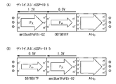


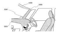


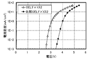


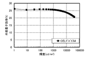


Classifications
-
- H—ELECTRICITY
- H10—SEMICONDUCTOR DEVICES; ELECTRIC SOLID-STATE DEVICES NOT OTHERWISE PROVIDED FOR
- H10K—ORGANIC ELECTRIC SOLID-STATE DEVICES
- H10K50/00—Organic light-emitting devices
- H10K50/10—OLEDs or polymer light-emitting diodes [PLED]
- H10K50/11—OLEDs or polymer light-emitting diodes [PLED] characterised by the electroluminescent [EL] layers
-
- H—ELECTRICITY
- H10—SEMICONDUCTOR DEVICES; ELECTRIC SOLID-STATE DEVICES NOT OTHERWISE PROVIDED FOR
- H10K—ORGANIC ELECTRIC SOLID-STATE DEVICES
- H10K30/00—Organic devices sensitive to infrared radiation, light, electromagnetic radiation of shorter wavelength or corpuscular radiation
- H10K30/20—Organic devices sensitive to infrared radiation, light, electromagnetic radiation of shorter wavelength or corpuscular radiation comprising organic-organic junctions, e.g. donor-acceptor junctions
-
- H—ELECTRICITY
- H10—SEMICONDUCTOR DEVICES; ELECTRIC SOLID-STATE DEVICES NOT OTHERWISE PROVIDED FOR
- H10K—ORGANIC ELECTRIC SOLID-STATE DEVICES
- H10K30/00—Organic devices sensitive to infrared radiation, light, electromagnetic radiation of shorter wavelength or corpuscular radiation
- H10K30/451—Organic devices sensitive to infrared radiation, light, electromagnetic radiation of shorter wavelength or corpuscular radiation comprising a metal-semiconductor-metal [m-s-m] structure
-
- H—ELECTRICITY
- H10—SEMICONDUCTOR DEVICES; ELECTRIC SOLID-STATE DEVICES NOT OTHERWISE PROVIDED FOR
- H10K—ORGANIC ELECTRIC SOLID-STATE DEVICES
- H10K50/00—Organic light-emitting devices
- H10K50/10—OLEDs or polymer light-emitting diodes [PLED]
- H10K50/14—Carrier transporting layers
- H10K50/15—Hole transporting layers
- H10K50/156—Hole transporting layers comprising a multilayered structure
-
- H—ELECTRICITY
- H10—SEMICONDUCTOR DEVICES; ELECTRIC SOLID-STATE DEVICES NOT OTHERWISE PROVIDED FOR
- H10K—ORGANIC ELECTRIC SOLID-STATE DEVICES
- H10K71/00—Manufacture or treatment specially adapted for the organic devices covered by this subclass
- H10K71/10—Deposition of organic active material
- H10K71/16—Deposition of organic active material using physical vapour deposition [PVD], e.g. vacuum deposition or sputtering
- H10K71/164—Deposition of organic active material using physical vapour deposition [PVD], e.g. vacuum deposition or sputtering using vacuum deposition
-
- H—ELECTRICITY
- H10—SEMICONDUCTOR DEVICES; ELECTRIC SOLID-STATE DEVICES NOT OTHERWISE PROVIDED FOR
- H10K—ORGANIC ELECTRIC SOLID-STATE DEVICES
- H10K71/00—Manufacture or treatment specially adapted for the organic devices covered by this subclass
- H10K71/10—Deposition of organic active material
- H10K71/16—Deposition of organic active material using physical vapour deposition [PVD], e.g. vacuum deposition or sputtering
- H10K71/166—Deposition of organic active material using physical vapour deposition [PVD], e.g. vacuum deposition or sputtering using selective deposition, e.g. using a mask
-
- H—ELECTRICITY
- H10—SEMICONDUCTOR DEVICES; ELECTRIC SOLID-STATE DEVICES NOT OTHERWISE PROVIDED FOR
- H10K—ORGANIC ELECTRIC SOLID-STATE DEVICES
- H10K85/00—Organic materials used in the body or electrodes of devices covered by this subclass
- H10K85/60—Organic compounds having low molecular weight
- H10K85/631—Amine compounds having at least two aryl rest on at least one amine-nitrogen atom, e.g. triphenylamine
- H10K85/633—Amine compounds having at least two aryl rest on at least one amine-nitrogen atom, e.g. triphenylamine comprising polycyclic condensed aromatic hydrocarbons as substituents on the nitrogen atom
-
- H—ELECTRICITY
- H10—SEMICONDUCTOR DEVICES; ELECTRIC SOLID-STATE DEVICES NOT OTHERWISE PROVIDED FOR
- H10K—ORGANIC ELECTRIC SOLID-STATE DEVICES
- H10K2101/00—Properties of the organic materials covered by group H10K85/00
- H10K2101/20—Delayed fluorescence emission
-
- H—ELECTRICITY
- H10—SEMICONDUCTOR DEVICES; ELECTRIC SOLID-STATE DEVICES NOT OTHERWISE PROVIDED FOR
- H10K—ORGANIC ELECTRIC SOLID-STATE DEVICES
- H10K2101/00—Properties of the organic materials covered by group H10K85/00
- H10K2101/30—Highest occupied molecular orbital [HOMO], lowest unoccupied molecular orbital [LUMO] or Fermi energy values
-
- H—ELECTRICITY
- H10—SEMICONDUCTOR DEVICES; ELECTRIC SOLID-STATE DEVICES NOT OTHERWISE PROVIDED FOR
- H10K—ORGANIC ELECTRIC SOLID-STATE DEVICES
- H10K2101/00—Properties of the organic materials covered by group H10K85/00
- H10K2101/40—Interrelation of parameters between multiple constituent active layers or sublayers, e.g. HOMO values in adjacent layers
-
- H—ELECTRICITY
- H10—SEMICONDUCTOR DEVICES; ELECTRIC SOLID-STATE DEVICES NOT OTHERWISE PROVIDED FOR
- H10K—ORGANIC ELECTRIC SOLID-STATE DEVICES
- H10K39/00—Integrated devices, or assemblies of multiple devices, comprising at least one organic radiation-sensitive element covered by group H10K30/00
- H10K39/30—Devices controlled by radiation
-
- H—ELECTRICITY
- H10—SEMICONDUCTOR DEVICES; ELECTRIC SOLID-STATE DEVICES NOT OTHERWISE PROVIDED FOR
- H10K—ORGANIC ELECTRIC SOLID-STATE DEVICES
- H10K59/00—Integrated devices, or assemblies of multiple devices, comprising at least one organic light-emitting element covered by group H10K50/00
- H10K59/10—OLED displays
- H10K59/12—Active-matrix OLED [AMOLED] displays
-
- H—ELECTRICITY
- H10—SEMICONDUCTOR DEVICES; ELECTRIC SOLID-STATE DEVICES NOT OTHERWISE PROVIDED FOR
- H10K—ORGANIC ELECTRIC SOLID-STATE DEVICES
- H10K59/00—Integrated devices, or assemblies of multiple devices, comprising at least one organic light-emitting element covered by group H10K50/00
- H10K59/80—Constructional details
- H10K59/87—Passivation; Containers; Encapsulations
Landscapes
- Physics & Mathematics (AREA)
- Optics & Photonics (AREA)
- Engineering & Computer Science (AREA)
- Electromagnetism (AREA)
- Microelectronics & Electronic Packaging (AREA)
- Manufacturing & Machinery (AREA)
- Spectroscopy & Molecular Physics (AREA)
- Chemical & Material Sciences (AREA)
- Materials Engineering (AREA)
- Electroluminescent Light Sources (AREA)
- Devices For Indicating Variable Information By Combining Individual Elements (AREA)
- Light Receiving Elements (AREA)
Abstract
Description
本発明の一態様は、有機化合物、有機半導体デバイス、発光素子、発光デバイス、有機ELデバイス、フォトダイオードセンサ、ディスプレイモジュール、照明モジュール、表示装置、発光装置、電子機器、照明装置および電子デバイスに関する。なお、本発明の一態様は、上記の技術分野に限定されない。本明細書等で開示する発明の一態様の技術分野は、物、方法、または、製造方法に関するものである。または、本発明の一態様は、プロセス、マシン、マニュファクチャ、または、組成物(コンポジション・オブ・マター)に関するものである。そのため、より具体的に本明細書で開示する本発明の一態様の技術分野としては、半導体装置、表示装置、液晶表示装置、発光装置、照明装置、蓄電装置、記憶装置、撮像装置、それらの駆動方法、または、それらの製造方法、を一例として挙げることができる。 One aspect of the present invention relates to an organic compound, an organic semiconductor device, a light emitting element, a light emitting device, an organic EL device, a photodiode sensor, a display module, a lighting module, a display device, a light emitting device, an electronic device, a lighting device and an electronic device. It should be noted that one aspect of the present invention is not limited to the above technical fields. The technical field of one aspect of the invention disclosed in the present specification and the like relates to a product, a method, or a manufacturing method. Alternatively, one aspect of the invention relates to a process, machine, manufacture, or composition (composition of matter). Therefore, more specifically, the technical fields of one aspect of the present invention disclosed in the present specification include semiconductor devices, display devices, liquid crystal display devices, light emitting devices, lighting devices, power storage devices, storage devices, image pickup devices, and the like. The driving method or the manufacturing method thereof can be given as an example.
有機化合物を用いたエレクトロルミネッセンス(EL:Electroluminescence)を利用する発光デバイス(有機ELデバイス)の実用化が進んでいる。これら有機ELデバイスの基本的な構成は、一対の電極間に発光材料を含む有機化合物層(EL層)を挟んだものである。このデバイスに電圧を印加して、キャリアを注入し、当該キャリアの再結合エネルギーを利用することにより、発光材料からの発光を得ることができる。 Practical use of light emitting devices (organic EL devices) that utilize electroluminescence (EL) using organic compounds is progressing. The basic configuration of these organic EL devices is such that an organic compound layer (EL layer) containing a light emitting material is sandwiched between a pair of electrodes. By applying a voltage to this device, injecting carriers, and utilizing the recombination energy of the carriers, light emission from the light emitting material can be obtained.
このような有機ELデバイスは自発光型であるためディスプレイの画素として用いると、液晶に比べ、視認性が高く、バックライトが不要である等の利点があり、フラットパネルディスプレイには特に好適である。また、このような有機ELデバイスを用いたディスプレイは、薄型軽量に作製できることも大きな利点である。さらに非常に応答速度が速いことも特徴の一つである。 Since such an organic EL device is a self-luminous type, when used as a pixel of a display, it has advantages such as higher visibility and no need for a backlight as compared with a liquid crystal display, and is particularly suitable for a flat panel display. .. Further, it is a great advantage that the display using such an organic EL device can be manufactured thin and lightweight. Another feature is that the response speed is extremely fast.
また、これらの有機ELデバイスは発光層を平面状に連続して形成することが可能であるため、面状に発光を得ることができる。これは、白熱電球、LEDに代表される点光源、あるいは蛍光灯に代表される線光源では得難い特色であるため、照明等に応用できる面光源としての利用価値も高い。 Further, since these organic EL devices can continuously form the light emitting layer in a plane, it is possible to obtain light emission in a plane shape. This is a feature that is difficult to obtain with an incandescent light bulb, a point light source represented by an LED, or a line light source represented by a fluorescent lamp, and therefore has high utility value as a surface light source that can be applied to lighting and the like.
このように有機ELデバイスを用いたディスプレイ、照明装置はさまざまな電子機器に好適であるが、より良好な特性を有する有機ELデバイスを求めて研究開発が進められている(例えば非特許文献1参照)。 As described above, displays and lighting devices using organic EL devices are suitable for various electronic devices, but research and development are underway in search of organic EL devices having better characteristics (see, for example, Non-Patent Document 1). ).
本発明の一態様では、駆動電圧の低い有機半導体デバイスを提供することを目的とする。または本発明の一態様では、駆動電圧の低い有機ELデバイスを提供することを目的とする。または、本発明の一態様では、駆動電圧の低いフォトダイオードセンサを提供することを目的とする。または、本発明の一態様では、消費電力の小さい発光装置、電子機器、表示装置、または電子デバイスのいずれかを提供することを目的とする。 One aspect of the present invention is to provide an organic semiconductor device having a low drive voltage. Alternatively, one aspect of the present invention is to provide an organic EL device having a low drive voltage. Alternatively, one aspect of the present invention is to provide a photodiode sensor having a low drive voltage. Alternatively, one aspect of the present invention is to provide any of a light emitting device, an electronic device, a display device, or an electronic device having low power consumption.
本発明は上述の課題のうちいずれか一を解決すればよいものとする。 The present invention shall solve any one of the above-mentioned problems.
本発明の一態様は、陽極と、陰極と、前記陽極と、前記陰極との間に位置する有機化合物を含む層と、を有し、前記有機化合物を含む層は、正孔輸送領域を有し、前記正孔輸送領域は、第1の層と、第2の層と、を有し、前記第1の層は、前記陽極と前記第2の層との間に位置し、蒸着膜の表面電位の電位勾配をGSP(mV/nm)とした場合、前記第1の層を構成する有機化合物のGSPから、前記第2の層を構成する有機化合物のGSPを引いた値が20(mV/nm)以下である有機半導体デバイスである。 One aspect of the present invention includes an anode, a cathode, a layer containing an organic compound located between the anode and the cathode, and the layer containing the organic compound has a hole transport region. However, the hole transport region has a first layer and a second layer, and the first layer is located between the anode and the second layer of the vapor-deposited film. When the potential gradient of the surface potential is GSP (mV / nm), the value obtained by subtracting the GSP of the organic compound constituting the second layer from the GSP of the organic compound constituting the first layer is 20 (mV). / Nm) or less.
または、本発明の他の一態様は、陽極と、陰極と、前記陽極と、前記陰極との間に位置する有機化合物を含む層と、を有し、前記有機化合物を含む層は、正孔輸送領域を有し、前記正孔輸送領域は、第1の層と、第2の層と、を有し、前記第1の層は、前記陽極と前記第2の層との間に位置し、蒸着膜の表面電位の電位勾配をGSP(mV/nm)とした場合、前記第1の層を構成する有機化合物のGSPから、前記第2の層を構成する有機化合物のGSPを引いた値が5(mV/nm)以下である有機半導体デバイスである。 Alternatively, another aspect of the present invention includes an electric potential, a cathode, a layer containing an organic compound located between the electric potential and the cathode, and the layer containing the organic compound is a hole. It has a transport region, the hole transport region has a first layer and a second layer, the first layer located between the anode and the second layer. When the potential gradient of the surface potential of the vapor deposition film is GSP (mV / nm), the value obtained by subtracting the GSP of the organic compound constituting the second layer from the GSP of the organic compound constituting the first layer. Is an organic semiconductor device having a value of 5 (mV / nm) or less.
または、本発明の他の一態様は、陽極と、陰極と、前記陽極と、前記陰極との間に位置する有機化合物を含む層と、を有し、前記有機化合物を含む層は、正孔輸送領域を有し、前記正孔輸送領域は、第1の層と、第2の層と、を有し、前記第1の層は、前記陽極と前記第2の層との間に位置し、蒸着膜の表面電位の電位勾配をGSP(mV/nm)とした場合、前記第1の層を構成する有機化合物のGSPから、前記第2の層を構成する有機化合物のGSPを引いた値が0(mV/nm)以下である有機半導体デバイスである。 Alternatively, another aspect of the present invention includes an electric potential, a cathode, a layer containing an organic compound located between the electric potential and the cathode, and the layer containing the organic compound is a hole. It has a transport region, the hole transport region has a first layer and a second layer, the first layer located between the anode and the second layer. When the potential gradient of the surface potential of the vapor deposition film is GSP (mV / nm), the value obtained by subtracting the GSP of the organic compound constituting the second layer from the GSP of the organic compound constituting the first layer. Is an organic semiconductor device having a value of 0 (mV / nm) or less.
または、本発明の他の一態様は、陽極と、陰極と、前記陽極と、前記陰極との間に位置する有機化合物を含む層と、を有し、前記有機化合物を含む層は、正孔輸送領域と、発光層と、を有し、前記正孔輸送領域は、前記陽極と前記発光層との間に位置し、前記正孔輸送領域は、第1の層と、第2の層と、を有し、前記第1の層は、前記陽極と前記第2の層との間に位置し、蒸着膜の表面電位の電位勾配をGSP(mV/nm)とした場合、前記第1の層を構成する有機化合物のGSPから、前記第2の層を構成する有機化合物のGSPを引いた値が20(mV/nm)以下である有機ELデバイスである。 Alternatively, another aspect of the present invention has an anode, a cathode, a layer containing an organic compound located between the anode and the cathode, and the layer containing the organic compound is a hole. It has a transport region and a light emitting layer, the hole transport region is located between the anode and the light emitting layer, and the hole transport region includes a first layer and a second layer. The first layer is located between the anode and the second layer, and when the potential gradient of the surface potential of the vapor deposition film is GSP (mV / nm), the first layer is described. It is an organic EL device in which the value obtained by subtracting the GSP of the organic compound constituting the second layer from the GSP of the organic compound constituting the layer is 20 (mV / nm) or less.
または、本発明の他の一態様は、陽極と、陰極と、前記陽極と、前記陰極との間に位置する有機化合物を含む層と、を有し、前記有機化合物を含む層は、正孔輸送領域と、発光層と、を有し、前記正孔輸送領域は、前記陽極と前記発光層との間に位置し、前記正孔輸送領域は、第1の層と、第2の層と、を有し、前記第1の層は、前記陽極と前記第2の層との間に位置し、蒸着膜の表面電位の電位勾配をGSP(mV/nm)とした場合、前記第1の層を構成する有機化合物のGSPから、前記第2の層を構成する有機化合物のGSPを引いた値が5(mV/nm)以下である有機ELデバイスである。 Alternatively, another aspect of the present invention has an anode, a cathode, a layer containing an organic compound located between the anode and the cathode, and the layer containing the organic compound is a hole. It has a transport region and a light emitting layer, the hole transport region is located between the anode and the light emitting layer, and the hole transport region includes a first layer and a second layer. The first layer is located between the anode and the second layer, and when the potential gradient of the surface potential of the vapor deposition film is GSP (mV / nm), the first layer is described. It is an organic EL device in which the value obtained by subtracting the GSP of the organic compound constituting the second layer from the GSP of the organic compound constituting the layer is 5 (mV / nm) or less.
または、本発明の他の一態様は、陽極と、陰極と、前記陽極と、前記陰極との間に位置する有機化合物を含む層と、を有し、前記有機化合物を含む層は、正孔輸送領域と、発光層と、を有し、前記正孔輸送領域は、前記陽極と前記発光層との間に位置し、前記正孔輸送領域は、第1の層と、第2の層と、を有し、前記第1の層は、前記陽極と前記第2の層との間に位置し、蒸着膜の表面電位の電位勾配をGSP(mV/nm)とした場合、前記第1の層を構成する有機化合物のGSPから、前記第2の層を構成する有機化合物のGSPを引いた値が0(mV/nm)以下である有機ELデバイスである。 Alternatively, another aspect of the present invention has an anode, a cathode, a layer containing an organic compound located between the anode and the cathode, and the layer containing the organic compound is a hole. It has a transport region and a light emitting layer, the hole transport region is located between the anode and the light emitting layer, and the hole transport region includes a first layer and a second layer. The first layer is located between the anode and the second layer, and when the potential gradient of the surface potential of the vapor deposition film is GSP (mV / nm), the first layer is described. It is an organic EL device in which the value obtained by subtracting the GSP of the organic compound constituting the second layer from the GSP of the organic compound constituting the layer is 0 (mV / nm) or less.
または、本発明の他の一態様は、上記構成において、発光層と第2の層とが接している有機ELデバイスである。 Alternatively, another aspect of the present invention is an organic EL device in which the light emitting layer and the second layer are in contact with each other in the above configuration.
または、本発明の他の一態様は、陽極と、陰極と、前記陽極と、前記陰極との間に位置する有機化合物を含む層と、を有し、前記有機化合物を含む層は、活性層と、正孔輸送領域を有し、前記正孔輸送領域は、前記活性層と前記陰極との間に位置し、前記正孔輸送領域は、第1の層と、第2の層と、を有し、前記第1の層は、前記陽極と前記第2の層との間に位置し、蒸着膜の表面電位の電位勾配をGSP(mV/nm)とした場合、前記第1の層を構成する有機化合物のGSPから、前記第2の層を構成する有機化合物のGSPを引いた値が20(mV/nm)以下であるフォトダイオードセンサである。 Alternatively, another aspect of the present invention has an anode, a cathode, a layer containing an organic compound located between the anode and the cathode, and the layer containing the organic compound is an active layer. The hole transport region is located between the active layer and the cathode, and the hole transport region includes a first layer and a second layer. The first layer is located between the anode and the second layer, and when the potential gradient of the surface potential of the vapor deposition film is GSP (mV / nm), the first layer is used. It is a photodiode sensor in which the value obtained by subtracting the GSP of the organic compound constituting the second layer from the GSP of the constituent organic compound is 20 (mV / nm) or less.
または、本発明の他の一態様は、陽極と、陰極と、前記陽極と、前記陰極との間に位置する有機化合物を含む層と、を有し、前記有機化合物を含む層は、活性層と、正孔輸送領域を有し、前記正孔輸送領域は、前記活性層と前記陰極との間に位置し、前記正孔輸送領域は、第1の層と、第2の層と、を有し、前記第1の層は、前記陽極と前記第2の層との間に位置し、蒸着膜の表面電位の電位勾配をGSP(mV/nm)とした場合、前記第1の層を構成する有機化合物のGSPから、前記第2の層を構成する有機化合物のGSPを引いた値が5(mV/nm)以下であるフォトダイオードセンサである。 Alternatively, another aspect of the present invention has an anode, a cathode, a layer containing an organic compound located between the anode and the cathode, and the layer containing the organic compound is an active layer. The hole transport region is located between the active layer and the cathode, and the hole transport region includes a first layer and a second layer. The first layer is located between the anode and the second layer, and when the potential gradient of the surface potential of the vapor deposition film is GSP (mV / nm), the first layer is used. It is a photodiode sensor in which the value obtained by subtracting the GSP of the organic compound constituting the second layer from the GSP of the constituent organic compound is 5 (mV / nm) or less.
または、本発明の他の一態様は、陽極と、陰極と、前記陽極と、前記陰極との間に位置する有機化合物を含む層と、を有し、前記有機化合物を含む層は、活性層と、正孔輸送領域を有し、前記正孔輸送領域は、前記活性層と前記陰極との間に位置し、前記正孔輸送領域は、第1の層と、第2の層と、を有し、前記第1の層は、前記陽極と前記第2の層との間に位置し、蒸着膜の表面電位の電位勾配をGSP(mV/nm)とした場合、前記第1の層を構成する有機化合物のGSPから、前記第2の層を構成する有機化合物のGSPを引いた値が0(mV/nm)以下であるフォトダイオードセンサである。 Alternatively, another aspect of the present invention has an anode, a cathode, a layer containing an organic compound located between the anode and the cathode, and the layer containing the organic compound is an active layer. The hole transport region is located between the active layer and the cathode, and the hole transport region includes a first layer and a second layer. The first layer is located between the anode and the second layer, and when the potential gradient of the surface potential of the vapor deposition film is GSP (mV / nm), the first layer is used. It is a photodiode sensor in which the value obtained by subtracting the GSP of the organic compound constituting the second layer from the GSP of the constituent organic compound is 0 (mV / nm) or less.
または、本発明の他の一態様は、上記構成において、活性層と第1の層とが接しているフォトダイオードセンサである。 Alternatively, another aspect of the present invention is a photodiode sensor in which the active layer and the first layer are in contact with each other in the above configuration.
または、本発明の他の一態様は、上記構成において、第1の層と第2の層とが接している有機半導体デバイス、有機ELデバイスまたはフォトダイオードセンサである。 Alternatively, another aspect of the present invention is an organic semiconductor device, an organic EL device, or a photodiode sensor in which the first layer and the second layer are in contact with each other in the above configuration.
または、本発明の他の一態様は、上記いずれかに記載の有機半導体デバイス、有機ELデバイスまたはフォトダイオードセンサを備えた照明装置である。 Alternatively, another aspect of the present invention is a lighting device including the organic semiconductor device, the organic EL device, or the photodiode sensor according to any one of the above.
または、本発明の他の一態様は、上記いずれかに記載の有機半導体デバイス、有機ELデバイスまたはフォトダイオードセンサを備えた表示装置である。 Alternatively, another aspect of the present invention is a display device including the organic semiconductor device, the organic EL device, or the photodiode sensor according to any one of the above.
または、本発明の他の一態様は、上記いずれかに記載の有機半導体デバイス、有機ELデバイスまたはフォトダイオードセンサを備えた電子機器である。 Alternatively, another aspect of the present invention is an electronic device provided with the organic semiconductor device, organic EL device or photodiode sensor according to any one of the above.
または、本発明の他の一態様は、上記いずれかに記載の有機ELデバイスにおいて、前記正孔輸送領域と前記発光層の端面が概略同一平面上にある有機ELデバイスである。 Alternatively, another aspect of the present invention is the organic EL device according to any one of the above, wherein the hole transport region and the end face of the light emitting layer are substantially on the same plane.
または、本発明の他の一態様は、上記いずれかに記載の有機ELデバイスと、センサ、操作ボタン、スピーカ、または、マイクと、を有する電子機器である。 Alternatively, another aspect of the present invention is an electronic device having the organic EL device according to any one of the above and a sensor, an operation button, a speaker, or a microphone.
または、本発明の他の一態様は、上記いずれかに記載の有機ELデバイスと、トランジスタ、または、基板と、を有する発光装置である。 Alternatively, another aspect of the present invention is a light emitting device having the organic EL device according to any one of the above, a transistor, or a substrate.
または、本発明の他の一態様は、上記いずれかに記載の有機ELデバイスと、筐体と、を有する照明装置である。 Alternatively, another aspect of the present invention is a lighting device having the organic EL device according to any one of the above and a housing.
なお、本明細書中における発光装置とは、発光デバイスを用いた画像表示デバイスを含む。また、発光デバイスにコネクター、例えば異方導電性フィルム又はTCP(Tape Carrier Package)が取り付けられたモジュール、TCPの先にプリント配線板が設けられたモジュール、又は発光デバイスにCOG(Chip On Glass)方式によりIC(集積回路)が直接実装されたモジュールも発光装置に含む場合がある。さらに、照明器具等は、発光装置を有する場合がある。 The light emitting device in the present specification includes an image display device using a light emitting device. Further, a module in which a connector, for example, an anisotropic conductive film or TCP (Tape Carrier Package) is attached to the light emitting device, a module in which a printed wiring board is provided at the end of TCP, or a COG (Chip On Glass) method in the light emitting device. A module in which an IC (integrated circuit) is directly mounted may also be included in the light emitting device. Further, lighting equipment and the like may have a light emitting device.
本発明の一態様では、駆動電圧の低い有機半導体デバイスを提供することができる。または本発明の一態様では、駆動電圧の低い有機ELデバイスを提供することができる。または、本発明の一態様では、駆動電圧の低いフォトダイオードセンサを提供することができる。または、本発明の一態様では、消費電力の小さい発光装置、電子機器、表示装置、または電子デバイスのいずれかを提供することができる。 In one aspect of the present invention, it is possible to provide an organic semiconductor device having a low drive voltage. Alternatively, in one aspect of the present invention, it is possible to provide an organic EL device having a low drive voltage. Alternatively, in one aspect of the present invention, a photodiode sensor having a low drive voltage can be provided. Alternatively, in one aspect of the present invention, any of a light emitting device, an electronic device, a display device, or an electronic device having low power consumption can be provided.
なお、これらの効果の記載は、他の効果の存在を妨げるものではない。なお、本発明の一態様は、必ずしも、これらの効果の全てを有する必要はない。なお、これら以外の効果は、明細書、図面、請求項などの記載から、自ずと明らかとなるものであり、明細書、図面、請求項などの記載から、これら以外の効果を抽出することが可能である。 The description of these effects does not preclude the existence of other effects. It should be noted that one aspect of the present invention does not necessarily have to have all of these effects. It should be noted that the effects other than these are self-evident from the description of the description, drawings, claims, etc., and it is possible to extract the effects other than these from the description of the description, drawings, claims, etc. Is.
以下、本発明の実施の態様について図面を用いて詳細に説明する。但し、本発明は以下の説明に限定されず、本発明の趣旨及びその範囲から逸脱することなくその形態及び詳細を様々に変更し得ることは当業者であれば容易に理解される。従って、本発明は以下に示す実施の形態の記載内容に限定して解釈されるものではない。 Hereinafter, embodiments of the present invention will be described in detail with reference to the drawings. However, the present invention is not limited to the following description, and it is easily understood by those skilled in the art that the form and details of the present invention can be variously changed without departing from the spirit and scope of the present invention. Therefore, the present invention is not construed as being limited to the description of the embodiments shown below.
なお、本明細書等において、メタルマスク、またはFMM(ファインメタルマスク、高精細なメタルマスク)を用いて作製されるデバイスをMM(メタルマスク)構造のデバイスと呼称する場合がある。また、本明細書等において、メタルマスク、またはFMMを用いることなく作製されるデバイスをMML(メタルマスクレス)構造のデバイスと呼称する場合がある。 In the present specification and the like, a metal mask or a device manufactured by using an FMM (fine metal mask, high-definition metal mask) may be referred to as a device having an MM (metal mask) structure. Further, in the present specification and the like, a device manufactured without using a metal mask or FMM may be referred to as a device having an MML (metal maskless) structure.
(実施の形態1)
有機ELデバイスは、有機薄膜を用いた有機半導体デバイスの一種である。有機半導体デバイスとしては他にフォトダイオードセンサ、有機TFTなどが代表的である。
(Embodiment 1)
The organic EL device is a kind of organic semiconductor device using an organic thin film. Other typical organic semiconductor devices include photodiode sensors and organic TFTs.
このような有機半導体デバイスに用いられる有機薄膜の多くは、蒸着法により形成されている。成膜したい有機化合物に熱などのエネルギーを加えて昇華させる蒸着法により成膜された有機薄膜は、一部の結晶化しやすい材料の膜を除き長らく非晶質のアモルファスであり、ランダム配向であるとされてきた。 Most of the organic thin films used in such organic semiconductor devices are formed by a vapor deposition method. The organic thin film formed by the vapor deposition method in which energy such as heat is applied to the organic compound to be formed into a film is amorphous for a long time except for a film of a material that is easily crystallized, and has a random orientation. Has been said.
しかし近年、多くの分光学的研究により、非晶質の有機薄膜においても緩い分子配向が存在する場合があり、デバイスの特性に影響を与えていることが知られるようになった。例えば、有機ELデバイスにおいて、発光物質の双極子モーメントが発光面に対して水平に配向しやすい物質は発光の取り出しが容易であり発光効率の高い発光素子を提供しやすいこと、配向によるπ軌道の重ね合わせが起こりやすい物質は導電率が高い傾向にあること、などが知られている。 However, in recent years, many spectroscopic studies have revealed that even in amorphous organic thin films, loose molecular orientations may exist, which affects the characteristics of the device. For example, in an organic EL device, a substance in which the bipolar moment of the light emitting substance is easily oriented horizontally with respect to the light emitting surface is easy to take out light emission and is easy to provide a light emitting element having high luminous efficiency. It is known that substances that are prone to superposition tend to have high conductivity.
ところで、有機化合物には極性分子と無極性分子が存在し、極性分子は永久双極子モーメントを有している。極性分子を蒸着した場合、蒸着膜がランダム配向であればこれら極性の偏りは相殺され膜内に分子の極性を由来とする分極は発生しない。しかし、当該蒸着膜が前述のように分子配向を有する場合、分極の偏りに由来する巨大表面電位(Giant Surface Potential)が現れることがある。 By the way, polar molecules and non-polar molecules exist in organic compounds, and polar molecules have a permanent dipole moment. When polar molecules are vapor-deposited, if the vapor-film deposition film is randomly oriented, these polar biases are canceled out and polarization derived from the polarity of the molecule does not occur in the film. However, when the vapor-filmed film has a molecular orientation as described above, a huge surface potential (Giant Surface Potential) derived from the bias of the polarization may appear.
巨大表面電位とは、蒸着膜の表面電位が膜厚に比例して増加する現象である。その大きさを膜厚に依存しない数値として扱うには、蒸着膜の表面電位を膜厚で割った値、すなわち、蒸着膜の表面電位の電位勾配(傾き)を用いればよい。本明細書中では、この蒸着膜の表面電位の電位勾配をGSP(mV/nm)と記載する。 Giant surface potential is a phenomenon in which the surface potential of a thin-film vapor deposition film increases in proportion to the film thickness. In order to treat the size as a numerical value independent of the film thickness, a value obtained by dividing the surface potential of the vapor-film deposition film by the film thickness, that is, the potential gradient (slope) of the surface potential of the vapor-film deposition film may be used. In the present specification, the potential gradient of the surface potential of this thin-film deposition film is referred to as GSP (mV / nm).
巨大表面電位により蒸着膜の表面電位は、飽和することなく膜厚の増加に伴って一定の割合で増加する。例えば、トリス(8-キノリノラト)アルミニウム(略称:Alq3)の蒸着膜は、560nmの膜厚での表面電位が約28Vにも達する。 Due to the huge surface potential, the surface potential of the vapor-film vapor film increases at a constant rate as the film thickness increases without being saturated. For example, a vapor-deposited film of tris (8-quinolinolat) aluminum (abbreviation: Alq 3 ) has a surface potential of about 28 V at a film thickness of 560 nm.
巨大表面電位は、有機化合物の永久双極子モーメントが、膜厚方向にわずかに偏ることによる自発的配向分極現象として説明できる。Alq3は、永久双極子モーメントの配向が、膜厚方向に配向オーダーパラメーター(cosθ:θは膜の法線方向からの永久双極子モーメントの傾き角)で0.05と、わずかに配向した非晶質膜であるが、このわずかな配向が大きな分極を生み出し、GSPが発現する原因となっていると言われている。この配向分極により生じる電界強度は5×10⁵V/cmにも達し、これは一般的な有機薄膜デバイスの駆動中の電界強度と同程度の大きさである。 The giant surface potential can be explained as a spontaneous orientation polarization phenomenon due to the permanent dipole moment of the organic compound being slightly biased in the film thickness direction. In Alq 3 , the orientation of the permanent dipole moment is slightly oriented, with the orientation order parameter in the film thickness direction (cos θ: θ is the inclination angle of the permanent dipole moment from the normal direction of the film), which is 0.05. Although it is a crystalline film, it is said that this slight orientation produces a large polarization and causes the expression of GSP. The electric field strength generated by this orientation polarization reaches as high as 5 × 10⁵ V / cm, which is about the same as the electric field strength during driving of a general organic thin film device.
今回、本発明者らは、有機化合物の薄膜の積層構造を用いた有機半導体デバイス(有機ELデバイス、フォトダイオードセンサなど)において、ホールをキャリアとする層(正孔輸送層)が複数層接して設けられている場合、接して積層された2つの層各々のGSPの差(ΔGSP(mV/nm))がホールの注入能力に関係し、デバイスの駆動電圧に大きな影響を与えることを見出した。 Here, the present inventors have formed a plurality of layers (hole transport layers) having holes as carriers in contact with organic semiconductor devices (organic EL devices, photodiode sensors, etc.) using a laminated structure of thin films of organic compounds. It has been found that, when provided, the difference in GSP (ΔGSP (mV / nm)) between the two layers stacked in contact with each other is related to the hole injection capacity and has a great influence on the drive voltage of the device.
図1に、ホールのみをキャリアとした有機半導体デバイス(デバイス1乃至デバイス3)における、ΔGSPと電流密度-電圧特性との関係を検証した結果を示す。また、デバイス1乃至デバイス3のデバイス構造、用いた材料、各々のGSPおよびΔGSPをまとめた表を以下に示す。
FIG. 1 shows the results of verifying the relationship between ΔGSP and the current density-voltage characteristics in organic semiconductor devices (
なお、デバイス1乃至デバイス3における「接して積層された2つの層」とは、下記表における層2および層3に相当する。
The "two layers in contact with each other" in the


表中、ITSOは酸化珪素を含むインジウム錫酸化物であり、OCHD-003は分子量672でフッ素を含む電子アクセプタ材料、HTM-1は正孔輸送性の有機化合物、Alはアルミニウムである。また、mmtBuBioFBi、mmtBumTPoFBi-02、およびmmtBumBioFBiの分子構造を以下に示す。なお、層1から陰極は陽極側から真空蒸着法により形成した。
In the table, ITSO is an indium tin oxide containing silicon oxide, OCHD-003 is an electron acceptor material having a molecular weight of 672 and containing fluorine, HTM-1 is a hole-transporting organic compound, and Al is aluminum. In addition, the molecular structures of mmtBuBioFBi, mmtBumTPoFBi-02, and mmtBumBioFBi are shown below. The cathode from

図1に示すように、ΔGSPの小さいデバイスほど電流密度-電圧特性が0Vに近い電圧で立ち上がってきており、ホールの注入性が良好であることがわかる。また、本発明者らは同時に、ΔGSPが20(mV/nm)以下であることで、有機半導体デバイスにおいて十分に良好なホール注入性を得られることも見出した。 As shown in FIG. 1, it can be seen that the device having a smaller ΔGSP has a current density-voltage characteristic rising at a voltage closer to 0 V, and the hole injection property is better. At the same time, the present inventors have also found that a sufficiently good hole injection property can be obtained in an organic semiconductor device when ΔGSP is 20 (mV / nm) or less.
すなわち、本発明の一態様は、接して積層された少なくとも2つの層(第1の正孔輸送層、第2の正孔輸送層)を有する有機半導体デバイスにおいて、第1の正孔輸送層側から第2の正孔輸送層側に向かってホールが流れる場合、第1の正孔輸送層を構成する有機化合物のGSP(GSP1)と、第2の正孔輸送層を構成する有機化合物のGSP(GSP2)の差ΔGSP(GSP1-GSP2)が20(mV/nm)以下である有機半導体デバイスである。 That is, one aspect of the present invention is the first hole transport layer side in an organic semiconductor device having at least two layers (first hole transport layer, second hole transport layer) laminated in contact with each other. When holes flow from the hole to the second hole transport layer side, the organic compound GSP (GSP1) constituting the first hole transport layer and the organic compound GSP constituting the second hole transport layer This is an organic semiconductor device in which the difference ΔGSP (GSP1-GSP2) of (GSP2) is 20 (mV / nm) or less.
このような構成を有する有機半導体デバイスは、ホールの注入が容易であり、駆動電圧の低い有機半導体デバイスとすることが可能となる。 An organic semiconductor device having such a configuration can easily inject holes and can be an organic semiconductor device having a low drive voltage.
なお、ΔGSPは、第1の正孔輸送層または第2の正孔輸送層の膜厚が厚い場合、より小さいことが好ましい。具体的には、第1の正孔輸送層が80nm以上160nm以下である場合15(mV/nm)以下であることが好ましく、第2の正孔輸送層が20nm以上140nm以下である場合、10(mV/nm)以下であることが好ましい。 The ΔGSP is preferably smaller when the film thickness of the first hole transport layer or the second hole transport layer is thick. Specifically, when the first hole transport layer is 80 nm or more and 160 nm or less, it is preferably 15 (mV / nm) or less, and when the second hole transport layer is 20 nm or more and 140 nm or less, 10 It is preferably (mV / nm) or less.
また、膜厚に関係なく、ΔGSPは5(mV/nm)以下であることがより好ましく、さらに好ましくは0(mV/nm)以下であり、ΔGSPが負となる構成が最も好ましい。 Further, regardless of the film thickness, the ΔGSP is more preferably 5 (mV / nm) or less, more preferably 0 (mV / nm) or less, and the configuration in which ΔGSP is negative is most preferable.
次に、デバイス4乃至デバイス7の容量-電圧特性を測定した結果(図2)、電流密度-電圧特性を測定した結果(図3)および図4を参照しながら、蒸着膜の分極およびGSPがホールの注入性に与える影響について説明する。
Next, with reference to the results of measuring the capacitance-voltage characteristics of the
デバイス4乃至デバイス7のデバイス構造およびデバイス5およびデバイス6に用いた有機化合物のGSP、ΔGSPを下表に示した。なお、デバイス4乃至デバイス7における「接して積層された2つの層」とは、下記表における層2および層3に相当する。なお、デバイス4とデバイス7は層2と層3が同じ材料で構成されていることから、ΔGSPは0である。
The device structures of the


図2の容量-電圧特性より、デバイス4とデバイス7は各々同一材料で構成される層2及び層3にまずホールが注入し、閾値電圧である2V付近まで層4に電荷が蓄積していることが分かる。デバイス4とデバイス7のホール注入電圧は層2(層3)の自発分極の大きさ(GSP)により決まる。
From the capacitance-voltage characteristics of FIG. 2, in the
デバイス5は閾値電圧を過ぎても容量変化がほとんどなく、ホールが注入しにくいことが容量-電圧特性(図2)から分かる。また電流密度-電圧特性においてもデバイス5は、デバイス4、デバイス6およびデバイス7と比較して電流を流しにくいことが見て取れる(図3)。
It can be seen from the capacitance-voltage characteristics (FIG. 2) that the
一方、デバイス6ではまず層2に、続いて層3に、と二段階でホールが注入し、閾値電圧付近では層4に電荷が蓄積している様子が容量-電圧特性(図2)から分かる。
On the other hand, in the
デバイス5とデバイス6は層2と層3のGSPの大小関係が逆であり、層2を構成する有機化合物と層3を構成する有機化合物のGSPの差(層2-層3)(ΔGSP)が負であるデバイス6の方がホール注入に有利であり、すなわちΔGSPが小さい方がホール注入に優れていると言える(図4)。
In the
このように、有機半導体デバイスでは、接して積層された正孔輸送層を構成する有機化合物のGSPの関係が正孔の注入性に大きな影響を与え、適切な組み合わせを選択することによって、より良好な特性を有する有機半導体デバイスを容易に得ることができるようになる。 As described above, in an organic semiconductor device, the relationship between GSPs of organic compounds constituting the contact-stacked hole transport layers has a great influence on the hole injectability, and it is better by selecting an appropriate combination. It becomes possible to easily obtain an organic semiconductor device having various characteristics.
有機半導体デバイスの正孔輸送領域では、電極とのホール授受を考慮すると、活性層または発光層との間で異なるHOMO準位を有する有機化合物からなる層にホールを順次注入してゆく必要がある。当然、各層間におけるHOMO準位の差が大きすぎると駆動電圧が高くなってしまうため、電極と活性層(発光層)の間にはそれらのHOMO準位の間に位置するようなHOMO準位を有する有機化合物からなる層を配置することでHOMO準位の差を緩和している。しかし、HOMO準位の差がさほど大きくない層同士であっても、用いる有機化合物の組み合わせによっては大きく駆動電圧が上がってしまう場合があった。これまでそれを回避するための指針はなく、材料同士の相性として片づけられて来た。本発明の構成を適用することで、そのようなミスマッチを解消し、容易に特性の良好な有機半導体デバイスを得ることができるようになる。 In the hole transport region of an organic semiconductor device, it is necessary to sequentially inject holes into a layer made of an organic compound having a different HOMO level between the active layer and the light emitting layer in consideration of hole transfer with the electrode. .. Naturally, if the difference between the HOMO levels between the layers is too large, the drive voltage will be high, so the HOMO levels located between the electrodes and the active layer (light emitting layer) are located between the HOMO levels. By arranging a layer made of an organic compound having HOMO, the difference in HOMO level is alleviated. However, even in layers where the difference in HOMO level is not so large, the drive voltage may increase significantly depending on the combination of organic compounds used. So far, there is no guideline to avoid it, and it has been dismissed as compatibility between materials. By applying the configuration of the present invention, such a mismatch can be eliminated and an organic semiconductor device having good characteristics can be easily obtained.
続いて、本発明の一態様の有機半導体デバイスの構成について説明する。図5(A)に、本発明の一態様の有機半導体デバイスの模式図を示した。本発明の一態様の有機半導体デバイスは、陽極10および陰極30の間に、有機化合物を含む層50が設けられており、有機化合物を含む層50は少なくとも第1の正孔輸送層21と第2の正孔輸送層22とを有している。ホールは、第1の正孔輸送層側から第2の正孔輸送層側へと流れる構成となっており、本発明の一態様の有機半導体デバイスは、第1の正孔輸送層21を構成する有機化合物のGSP(GSP1)と第2の正孔輸送層22を構成する有機化合物のGSP(GSP2)との差ΔGSP(GSP1-GSP2)が20(mV/nm)以下の有機半導体デバイスである。ΔGSPが20(mV/nm)以下であることによって、本発明の一態様の有機半導体デバイスはホールの注入性が良好なデバイスとすることが可能となり、駆動電圧の小さい有機半導体デバイスとすることが容易となる。なお、ΔGSPは5(mV/nm)以下であることがより好ましく、0(mV/nm)以下であることがさらに好ましい。
Subsequently, the configuration of the organic semiconductor device according to one aspect of the present invention will be described. FIG. 5A shows a schematic diagram of an organic semiconductor device according to an aspect of the present invention. In the organic semiconductor device of one aspect of the present invention, a
有機半導体デバイスとしては、有機TFT、有機ELデバイス、フォトダイオードセンサなど様々なデバイスが存在するが、本発明の一態様は、正孔輸送層の積層を有するどのような有機半導体デバイスにも適用することが可能である。 As the organic semiconductor device, there are various devices such as an organic TFT, an organic EL device, and a photodiode sensor, and one aspect of the present invention is applied to any organic semiconductor device having a stack of hole transport layers. It is possible.
有機半導体デバイスの例として、図5(B)に有機ELデバイス、図5(C)にフォトダイオードセンサへそれぞれ本発明を適用した図を示す。 As an example of the organic semiconductor device, FIG. 5B shows an organic EL device, and FIG. 5C shows a diagram in which the present invention is applied to a photodiode sensor.
図5(B)に示した本発明の一態様の有機ELデバイスでは、陽極10および陰極30との間に、EL層51(有機化合物を含む層50に相当)が設けられており、EL層51は、少なくとも正孔輸送層(第1の正孔輸送層21、第2の正孔輸送層22)および発光層40を有している。第1の正孔輸送層21は第2の正孔輸送層22よりも陽極10側に設けられており、第1の正孔輸送層21と第2の正孔輸送層22とは接して重なっている。また、発光層40は第2の正孔輸送層22と陰極30との間に位置しており、発光層40と第2の正孔輸送層22は接していることが好ましい。
In the organic EL device of one aspect of the present invention shown in FIG. 5B, an EL layer 51 (corresponding to a
図5(B)に示した有機ELデバイスでは、陽極10と発光層40との間が、キャリアをホールとする正孔輸送領域であり、陽極10側に第1の正孔輸送層21、発光層40側に第2の正孔輸送層22が位置しているため、キャリアであるホールは第1の正孔輸送層21から第2の正孔輸送層22に向かう方向に流れる。なお、第1の正孔輸送層21と陽極10との間には、陽極10からのホールの注入を容易とするために正孔注入層(図示せず)が設けられていても良い。
In the organic EL device shown in FIG. 5B, the space between the
発光層40と陰極30との間は、電子をキャリアとした電子輸送領域である。電子輸送領域の構成には特に限定はなく、電子をキャリアとして流すことができる層を形成すればよい。発光層40では、電子とホールが再結合することによって発生する再結合エネルギーにより発光物質が励起され発光が得られる。
The space between the light emitting
本発明の一態様の有機ELデバイスは、ΔGSP(第1の正孔輸送層21を構成する有機化合物のGSP(GSP1)-第2の正孔輸送層22を構成する有機化合物のGSP(GSP2))が20(mV/nm)以下であることによって、ホールの注入性が良好となり、駆動電圧の小さい良好な特性を有する発光デバイスとすることができる。
The organic EL device of one aspect of the present invention is ΔGSP (GSP (GSP1) of the organic compound constituting the first hole transport layer 21-GSP (GSP2) of the organic compound constituting the second
なお、ΔGSPは、第1の正孔輸送層21または第2の正孔輸送層22の膜厚が厚い場合、より小さいことが好ましい。すなわちΔGSPは、第1の正孔輸送層が80nm以上160nm以下である場合、15(mV/nm)以下であることが好ましく、第2の正孔輸送層が20nm以上140nm以下である場合、10(mV/nm)以下であることが好ましい。
The ΔGSP is preferably smaller when the film thickness of the first
なお、正孔輸送層20の膜厚に関係なく、ΔGSPは5(mV/nm)以下であることがより好ましく、さらに好ましくは0(mV/nm)以下である。
The ΔGSP is more preferably 5 (mV / nm) or less, still more preferably 0 (mV / nm) or less, regardless of the film thickness of the
また、図5(B)で表される本発明の一態様の有機ELデバイスにおいては、第1の正孔輸送層21を構成する有機化合物は、アルキル基を有する芳香族アミンであることが第1の正孔輸送層21の屈折率を低下させることができ、光の取り出し効率を向上させることができるため好ましい。これにより、当該有機ELデバイスは発光効率の良好な有機ELデバイスとすることが可能である。
Further, in the organic EL device of one aspect of the present invention represented by FIG. 5B, the organic compound constituting the first
また、第1の正孔輸送層21を構成する有機化合物は、フルオレン骨格、またはスピロフルオレン骨格を有する有機化合物であることが好ましい。なお、フルオレニルアミンはHOMO準位を上昇させる効果があるため、第1の正孔輸送層21を構成する有機化合物がフルオレン骨格を有する芳香族アミンである場合、当該アミンの窒素に3つのフルオレンが結合すると、HOMO準位が大きく上昇する可能性がある。この場合、周辺材料のHOMO準位との差が大きくなり、駆動電圧や信頼性等に影響を及ぼす可能性がある。したがって、第1の正孔輸送層21を構成する有機化合物がフルオレン骨格を有する芳香族アミンである場合、当該アミンの窒素に結合するフルオレン骨格は一または二であることがさらに好ましい。
Further, the organic compound constituting the first
また、第1の正孔輸送層21を構成する有機化合物は、カルバゾール骨格を有する有機化合物であることが好ましい。
Further, the organic compound constituting the first
また、第1の正孔輸送層21を構成する有機化合物は、HOMO準位が-5.45eVから-5.20eVの範囲の有機化合物であることが、正孔注入層や陽極10からのホール注入性が良好となるため好ましい。これにより当該有機ELデバイスは低電圧で駆動することが可能である。
Further, the organic compound constituting the first
また、第2の正孔輸送層22を構成する有機化合物は、アルキル基を有する芳香族アミンであることが第2の正孔輸送層22の屈折率を低下させることができ、光の取り出し効率を向上させることができるため好ましい。これにより、当該有機ELデバイスは発光効率の良好な有機ELデバイスとすることが可能である。
Further, when the organic compound constituting the second
また、第2の正孔輸送層22を構成する有機化合物は、ジベンゾフラン骨格、またはジベンゾチオフェン骨格を有する有機化合物であることが好ましい。
Further, the organic compound constituting the second
また、有機半導体デバイスは、第1の正孔輸送層21のHOMO準位(HOMO1)と第2の正孔輸送層22のHOMO準位(HOMO2)との差ΔHOMO(HOMO1-HOMO2)が-0.3eV以上0.3eV以下、より好ましくは-0.2eV以上0.2eV以下となる事が、第1の正孔輸送層21から第2の正孔輸送層22への正孔注入性が良好となるため好ましい。これにより当該有機ELデバイスは低電圧で駆動することが可能である。
Further, in the organic semiconductor device, the difference ΔHOMO (HOMO1-HOMO2) between the HOMO level (HOMO1) of the first
また、有機半導体デバイスにおけるΔGSPおよびΔHOMOは、いずれも第1の正孔輸送層21と第2の正孔輸送層22への正孔注入性を良好にするパラメーターであることから、ΔGSPが低い際にはΔHOMOの範囲がより広い領域においても低い駆動電圧を示し、ΔHOMOの範囲が狭い場合は、ΔGSPの値がより高い値においても、低い駆動電圧を示す。したがって、ΔGSPが0以下の構成において、ΔHOMOは-0.6eV以上、0.6eV以下が好ましい。ΔHOMOの範囲が、-0.2eV以上、0.2eV以下の構成においては、ΔGSPは20以下が好ましい。
Further, since ΔGSP and ΔHOMO in the organic semiconductor device are both parameters that improve the hole injection property into the first
図5(C)に示した本発明の一態様のフォトダイオードセンサでは、陽極10および陰極30との間に、光電変換層52(有機化合物を含む層50に相当)が設けられており、有機化合物を含む層は、少なくとも第1の正孔輸送層21、第2の正孔輸送層22および活性層41を有している。第1の正孔輸送層21は第2の正孔輸送層22よりも陽極10側に設けられており、第1の正孔輸送層21と第2の正孔輸送層22とは接して重なっている。また、活性層41は第1の正孔輸送層21と陽極10との間に位置している。
In the photodiode sensor of one aspect of the present invention shown in FIG. 5C, a photoelectric conversion layer 52 (corresponding to a
図5(C)に示したフォトダイオードセンサでは、陰極30と活性層41との間が、キャリアをホールとする正孔輸送領域であり、前述のように少なくとも第1の正孔輸送層21と第2の正孔輸送層22とを有する。第1の正孔輸送層21と第2の正孔輸送層22は接して積層されており、また、活性層41側に第1の正孔輸送層21、陰極30側に第2の正孔輸送層22が位置する。これにより、活性層41で発生したホールは第1の正孔輸送層21から第2の正孔輸送層22に向かう方向に流れる。
In the photodiode sensor shown in FIG. 5C, the space between the
活性層41と陽極10との間は、電子をキャリアとした電子輸送領域である。電子輸送領域の構成には特に限定はなく、電子をキャリアとして流すことができる層を形成すればよい。
The area between the
活性層41では、光が照射されることによって電子とホールが発生し、発生した電子とホールは、電圧の向きに従って電子が陽極10側、ホールが陰極30側に向かって流れる。
In the
本発明の一態様のフォトダイオードセンサは、ΔGSP(第1の正孔輸送層21を構成する有機化合物のGSP(GSP1)-第2の正孔輸送層22を構成する有機化合物のGSP(GSP2))が20(mV/nm)以下であることによって、ホールの注入性が良好となり、損失の小さい良好な特性を有するフォトダイオードセンサとすることができる。
The photodiode sensor of one aspect of the present invention is ΔGSP (GSP (GSP1) of the organic compound constituting the first hole transport layer 21-GSP (GSP2) of the organic compound constituting the second
なお、ΔGSPは、第1の正孔輸送層21または第2の正孔輸送層22の膜厚が厚い場合、より小さいことが好ましい。すなわちΔGSPは、第1の正孔輸送層が80nm以上160nm以下である場合、15(mV/nm)以下であることが好ましく、第2の正孔輸送層が20nm以上140nm以下である場合、10(mV/nm)以下であることが好ましい。
The ΔGSP is preferably smaller when the film thickness of the first
なお、正孔輸送層20の膜厚に関係なく、ΔGSPは5(mV/nm)以下であることがより好ましく、さらに好ましくは0(mV/nm)以下である。
The ΔGSP is more preferably 5 (mV / nm) or less, still more preferably 0 (mV / nm) or less, regardless of the film thickness of the
ここで、有機化合物のGSPを求める方法について説明する。 Here, a method for obtaining the GSP of an organic compound will be described.
蒸着膜の表面電位が膜厚に比例して増加する現象は、前述のように巨大表面電位と呼ばれる。一般にはケルビンプローブ測定による蒸着膜の表面電位を膜厚方向にプロットしたときの傾きが、巨大表面電位の大きさ、すなわち、GSP(mV/nm)として議論されているが、2つの異なる層が積層されている場合、その界面に蓄積する分極電荷密度(mC/m2)がGSPと関連して変化することを利用してGSPを見積もることができる。 The phenomenon in which the surface potential of the vapor-filmed film increases in proportion to the film thickness is called a giant surface potential as described above. Generally, the inclination when the surface potential of the vapor-deposited film measured by the Kelvin probe measurement is plotted in the film thickness direction is discussed as the magnitude of the huge surface potential, that is, GSP (mV / nm), but two different layers are discussed. When stacked, the GSP can be estimated by utilizing the fact that the polarization charge density (mC / m 2 ) accumulated at the interface changes in relation to the GSP.
非特許文献1には、異なる自発分極を持つ有機薄膜(薄膜1および薄膜2。ただし薄膜1が陽極側、薄膜2が陰極側に位置する。)を積層させ電流を流した場合、下記の式が成り立つことが示されている。
In


式(1)においてσifは分極電荷密度、Viはホール注入電圧、Vbiは閾値電圧、d2は薄膜2の膜厚、ε2は薄膜2の誘電率である。Vi、Vbiはデバイスの容量-電圧特性から見積もることができる。また、誘電率は常光屈折率no(633nm)の二乗を用いることができる。このように、容量-電圧特性から見積もったVi、Vbiと、屈折率より算出した薄膜2の誘電率ε2、および薄膜2の膜厚d2より、式(1)を用いて分極電荷密度σifを求めることができる。
In equation (1), σ if is the polarization charge density, Vi is the hole injection voltage, V bi is the threshold voltage, d 2 is the film thickness of the
続いて、式(2)において、σifは分極電荷密度、Pnは薄膜nのGSP、εnは薄膜nの誘電率である。ここで、上記式(1)より分極電荷密度σifを求めることができるため、薄膜2としてGSPが既知の物質を用いることで、薄膜1のGSPを見積もることができる。
Subsequently, in the equation (2), σ if is the polarization charge density, P n is the GSP of the thin film n, and ε n is the dielectric constant of the thin film n. Here, since the polarization charge density σ if can be obtained from the above equation (1), the GSP of the
そこで、薄膜2としてGSPが(48(mV/nm))と既知であるAlq3を用い、測定用のデバイスとしてデバイス8とデバイス9を作製し、デバイス8ではmmtBumTPoFBi-02、デバイス9ではNPBのGSPを求めた例を以下に示す。
Therefore, using Alq 3 whose GSP is known to be (48 (mV / nm)) as the
デバイス8およびデバイス9のデバイス構造は下表のとおりである。なお、デバイス8およびデバイス9の層1_1から陰極は、陽極側から真空蒸着法により、基板温度は室温、成膜レートは0.2nm/secから0.4nm/secの条件で形成した。なお、一つの層を形成する間は蒸着を止めることなく成膜を行った。デバイス8およびデバイス9においては、層2_1が薄膜1、層3_1が薄膜2に相当する。
The device structures of the
また、デバイス8およびデバイス9の容量-電圧特性を図6に示す。
Further, the capacitance-voltage characteristics of the

表6に、図6および式(1)、式(2)を用いて求めた、デバイス8(mmtBumTPoFBi-02)およびデバイス9(NPB)のホール注入電圧Vi、閾値電圧Vbi、分極電荷密度σif、GSPと、計算に用いた各材料の屈折率noを示す。なお、屈折率の測定は分光エリプソメーター(ジェー・エー・ウーラム・ジャパン社製M-2000U)を用いて行った。 In Table 6, the hole injection voltage Vi, the threshold voltage V bi , and the polarization charge density of the device 8 ( mmtBumTPoFBi -02) and the device 9 (NPB) obtained by using FIG. 6 and the formulas (1) and (2) are shown. σ if , GSP , and the refractive index no of each material used in the calculation are shown. The refractive index was measured using a spectroscopic ellipsometer (M-2000U manufactured by JA Woolam Japan Co., Ltd.).

なお、デバイス8、デバイス9とほぼ同じ構成を有し、Alq3の膜厚のみ80nmであるデバイス10、デバイス11を作製し、各々ホール注入電圧がデバイス8、デバイス9よりも低電圧シフトすることを確認している。つまり、このようなデバイスにおいては、ホールが先に注入し、Alq3との界面に分極電荷が蓄積していることが示唆される。また、デバイス10、デバイス11を用いて、デバイス8、デバイス9と同様にGSPの見積もりを行い、同じ結果になることを確認した。
It should be noted that the
このように、GSPが既知であるAlq3と、GSPを求めたい有機化合物を積層したデバイスを作製し、容量-電圧特性を測定することで、GSPを見積もることができる。 In this way, the GSP can be estimated by manufacturing a device in which Alq 3 whose GSP is known and an organic compound for which GSP is desired are laminated and measuring the capacitance-voltage characteristics.
なお、薄膜1または薄膜2に複数の有機化合物が含まれる場合、主として含まれる(例えば最も多く含まれる)有機化合物のGSPを「層を構成する有機化合物のGSP」とみなすことができる。あるいは、薄膜1または薄膜2に複数の有機化合物が含まれる場合、各々の有機化合物のGSPと含有率を算出し、その加重平均(GSP_ave)を「層を構成する有機化合物のGSP」と定義しても良い。
When the
(実施の形態2)
本実施の形態では、本発明の一態様の有機ELデバイスについて詳しく説明する。図7(A)に、本発明の一態様の有機ELデバイスを表す図を示す。本発明の一態様の有機ELデバイスは、陽極101、陰極102の間にEL層103を有している。EL層103は、発光層113と、少なくとも第1の正孔輸送層112-1と第2の正孔輸送層112-2とを含む正孔輸送層112を有している。発光層113と陽極101との間の領域は、ホールをキャリアとする正孔輸送領域、発光層113と陰極102との間の領域は電子をキャリアとする電子輸送領域である。
(Embodiment 2)
In this embodiment, the organic EL device of one aspect of the present invention will be described in detail. FIG. 7A shows a diagram showing an organic EL device according to an aspect of the present invention. The organic EL device of one aspect of the present invention has an
第1の正孔輸送層112-1と第2の正孔輸送層112-2は、陽極101側からこの順に接して形成されている。また、第2の正孔輸送層112-2は発光層113と接していることが好ましい。この場合第2の正孔輸送層112-2は電子ブロック層としても機能する場合がある。正孔輸送層112は第1の正孔輸送層112-1、第2の正孔輸送層112-2の他に第3、第4の正孔輸送層を含んでいても良い。
The first hole transport layer 112-1 and the second hole transport layer 112-2 are formed in contact with each other in this order from the
正孔輸送層112と陽極101との間には正孔注入層111を設けても良い。なお、図7(A)にはこれらに加えて電子輸送層114、電子注入層115が図示されているが、有機ELデバイスの構成はこれらに限られることはなく、キャリアブロック層、励起子ブロック層、電荷発生層等のその他の機能層を有していてもよい。
A
続いて、上述の有機ELデバイスの詳細な構造および材料の例について説明する。 Subsequently, an example of the detailed structure and material of the above-mentioned organic EL device will be described.
陽極101は、仕事関数の大きい(具体的には4.0eV以上)金属、合金、導電性化合物、およびこれらの混合物などを用いて形成することが好ましい。具体的には、例えば、酸化インジウム-酸化スズ(ITO:Indium Tin Oxide)、ケイ素若しくは酸化ケイ素を含有した酸化インジウム-酸化スズ、酸化インジウム-酸化亜鉛、酸化タングステン及び酸化亜鉛を含有した酸化インジウム(IWZO)等が挙げられる。これらの導電性金属酸化物膜は、通常スパッタリング法により成膜されるが、ゾル-ゲル法などを応用して作製しても構わない。作製方法の例としては、酸化インジウム-酸化亜鉛は、酸化インジウムに対し1~20wt%の酸化亜鉛を加えたターゲットを用いてスパッタリング法により形成する方法などがある。また、酸化タングステン及び酸化亜鉛を含有した酸化インジウム(IWZO)は、酸化インジウムに対し酸化タングステンを0.5~5wt%、酸化亜鉛を0.1~1wt%含有したターゲットを用いてスパッタリング法により形成することもできる。この他、金(Au)、白金(Pt)、ニッケル(Ni)、タングステン(W)、クロム(Cr)、モリブデン(Mo)、鉄(Fe)、コバルト(Co)、銅(Cu)、パラジウム(Pd)、または金属材料の窒化物(例えば、窒化チタン)等が挙げられる。グラフェンも用いることができる。なお、後述する複合材料をEL層103における陽極101と接する層に用いることで、仕事関数に関わらず、電極材料を選択することができるようになる。
The
正孔注入層111は、アクセプタ性を有する物質を含む層である。アクセプタ性を有する物質としては、有機化合物と無機化合物のいずれも用いることが可能である。
The
アクセプタ性を有する物質としては、電子吸引基(ハロゲン基、シアノ基など)を有する化合物を用いることができ、7,7,8,8-テトラシアノ-2,3,5,6-テトラフルオロキノジメタン(略称:F4-TCNQ)、クロラニル、2,3,6,7,10,11-ヘキサシアノ-1,4,5,8,9,12-ヘキサアザトリフェニレン(略称:HAT-CN)、1,3,4,5,7,8-ヘキサフルオロテトラシアノ-ナフトキノジメタン(略称:F6-TCNNQ)、2-(7-ジシアノメチレン-1,3,4,5,6,8,9,10-オクタフルオロ-7H-ピレン-2-イリデン)マロノニトリル等を挙げることができる。特に、HAT-CNのように複素原子を複数有する縮合芳香環に電子吸引基が結合している化合物が、熱的に安定であり好ましい。また、電子吸引基(特にフルオロ基のようなハロゲン基、シアノ基など)を有する[3]ラジアレン誘導体は、電子受容性が非常に高いため好ましく、具体的にはα,α’,α’’-1,2,3-シクロプロパントリイリデントリス[4-シアノ-2,3,5,6-テトラフルオロベンゼンアセトニトリル]、α,α’,α’’-1,2,3-シクロプロパントリイリデントリス[2,6-ジクロロ-3,5-ジフルオロ-4-(トリフルオロメチル)ベンゼンアセトニトリル]、α,α’,α’’-1,2,3-シクロプロパントリイリデントリス[2,3,4,5,6-ペンタフルオロベンゼンアセトニトリル]などが挙げられる。アクセプタ性を有する物質としては以上で述べた有機化合物以外にも、モリブデン酸化物、バナジウム酸化物、ルテニウム酸化物、タングステン酸化物、マンガン酸化物等を用いることができる。この他、フタロシアニン(略称:H2Pc)、銅フタロシアニン(CuPc)等のフタロシアニン系の錯体化合物、4,4’-ビス[N-(4-ジフェニルアミノフェニル)-N-フェニルアミノ]ビフェニル(略称:DPAB)、N,N’-ビス{4-[ビス(3-メチルフェニル)アミノ]フェニル}-N,N’-ジフェニル-(1,1’-ビフェニル)-4,4’-ジアミン(略称:DNTPD)等の芳香族アミン化合物、或いはポリ(3,4-エチレンジオキシチオフェン)/ポリ(スチレンスルホン酸)(PEDOT/PSS)等の高分子等によっても正孔注入層111を形成することができる。アクセプタ性を有する物質は、隣接する正孔輸送層(あるいは正孔輸送材料)から、電界の印加により電子を引き抜くことができる。
As the substance having acceptability, a compound having an electron-withdrawing group (halogen group, cyano group, etc.) can be used, and 7,7,8,8-tetracyano-2,3,5,6-tetrafluoroquinodimethane can be used. Methane (abbreviation: F4-TCNQ), chloranyl, 2,3,6,7,10,11 - hexaciano-1,4,5,8,9,12-hexazatriphenylene (abbreviation: HAT-CN), 1 , 3,4,5,7,8-Hexafluorotetracyano-naphthoquinodimethane (abbreviation: F6-TCNNQ), 2- (7-dicyanomethylene-1,3,4,5,6,8,9, 10-Octafluoro-7H-pyrene-2-iriden) malononitrile and the like can be mentioned. In particular, a compound such as HAT-CN in which an electron-withdrawing group is bonded to a condensed aromatic ring having a plurality of complex atoms is thermally stable and preferable. Further, the [3] radialene derivative having an electron-withdrawing group (particularly a halogen group such as a fluoro group, a cyano group, etc.) is preferable because it has very high electron acceptability, and specifically, α, α', α''. -1,2,3-Cyclopropanetriylidenes [4-cyano-2,3,5,6-tetrafluorobenzenenitrile], α, α', α''-1,2,3-cyclopropanetriylidene Tris [2,6-dichloro-3,5-difluoro-4- (trifluoromethyl) benzenenitrile], α, α', α''-1,2,3-cyclopropanetriylidentris [2,3 4,5,6-pentafluorobenzene acetonitrile] and the like. As the substance having acceptability, molybdenum oxide, vanadium oxide, ruthenium oxide, tungsten oxide, manganese oxide and the like can be used in addition to the organic compounds described above. In addition, phthalocyanine-based complex compounds such as phthalocyanine (abbreviation: H 2 Pc) and copper phthalocyanine (CuPc), 4,4'-bis [N- (4-diphenylaminophenyl) -N-phenylamino] biphenyl (abbreviation). : DPAB), N, N'-bis {4- [bis (3-methylphenyl) amino] phenyl} -N, N'-diphenyl- (1,1'-biphenyl) -4,4'-diamine (abbreviation) : The
また、正孔注入層111として、正孔輸送性を有する材料に上記アクセプタ性物質を含有させた複合材料を用いることもできる。なお、正孔輸送性を有する材料にアクセプタ性物質を含有させた複合材料を用いることにより、仕事関数に依らず電極を形成する材料を選ぶことができる。つまり、陽極101として仕事関数の大きい材料だけでなく、仕事関数の小さい材料も用いることができるようになる。
Further, as the
複合材料に用いる正孔輸送性を有する材料としては、芳香族アミン化合物、カルバゾール誘導体、芳香族炭化水素、高分子化合物(オリゴマー、デンドリマー、ポリマー等)など、種々の有機化合物を用いることができる。なお、複合材料に用いる正孔輸送性を有する材料としては、1×10⁻⁶cm2/Vs以上の正孔移動度を有する物質であることが好ましい。以下では、複合材料における正孔輸送性を有する材料として用いることのできる有機化合物を具体的に列挙する。 As the material having a hole transport property used for the composite material, various organic compounds such as an aromatic amine compound, a carbazole derivative, an aromatic hydrocarbon, and a polymer compound (oligomer, dendrimer, polymer, etc.) can be used. The hole-transporting material used for the composite material is preferably a substance having a hole mobility of 1 × 10⁻⁶ cm 2 / Vs or more. In the following, organic compounds that can be used as materials having hole transport properties in composite materials are specifically listed.
複合材料に用いることのできる芳香族アミン化合物としては、N,N’-ジ(p-トリル)-N,N’-ジフェニル-p-フェニレンジアミン(略称:DTDPPA)、4,4’-ビス[N-(4-ジフェニルアミノフェニル)-N-フェニルアミノ]ビフェニル(略称:DPAB)、N,N’-ビス{4-[ビス(3-メチルフェニル)アミノ]フェニル}-N,N’-ジフェニル-(1,1’-ビフェニル)-4,4’-ジアミン(略称:DNTPD)、1,3,5-トリス[N-(4-ジフェニルアミノフェニル)-N-フェニルアミノ]ベンゼン(略称:DPA3B)等を挙げることができる。カルバゾール誘導体としては、具体的には、3-[N-(9-フェニルカルバゾール-3-イル)-N-フェニルアミノ]-9-フェニルカルバゾール(略称:PCzPCA1)、3,6-ビス[N-(9-フェニルカルバゾール-3-イル)-N-フェニルアミノ]-9-フェニルカルバゾール(略称:PCzPCA2)、3-[N-(1-ナフチル)-N-(9-フェニルカルバゾール-3-イル)アミノ]-9-フェニルカルバゾール(略称:PCzPCN1)、4,4’-ジ(N-カルバゾリル)ビフェニル(略称:CBP)、1,3,5-トリス[4-(N-カルバゾリル)フェニル]ベンゼン(略称:TCPB)、9-[4-(10-フェニルアントラセン-9-イル)フェニル]-9H-カルバゾール(略称:CzPA)、1,4-ビス[4-(N-カルバゾリル)フェニル]-2,3,5,6-テトラフェニルベンゼン等を用いることができる。芳香族炭化水素としては、例えば、2-tert-ブチル-9,10-ジ(2-ナフチル)アントラセン(略称:t-BuDNA)、2-tert-ブチル-9,10-ジ(1-ナフチル)アントラセン、9,10-ビス(3,5-ジフェニルフェニル)アントラセン(略称:DPPA)、2-tert-ブチル-9,10-ビス(4-フェニルフェニル)アントラセン(略称:t-BuDBA)、9,10-ジ(2-ナフチル)アントラセン(略称:DNA)、9,10-ジフェニルアントラセン(略称:DPAnth)、2-tert-ブチルアントラセン(略称:t-BuAnth)、9,10-ビス(4-メチル-1-ナフチル)アントラセン(略称:DMNA)、2-tert-ブチル-9,10-ビス[2-(1-ナフチル)フェニル]アントラセン、9,10-ビス[2-(1-ナフチル)フェニル]アントラセン、2,3,6,7-テトラメチル-9,10-ジ(1-ナフチル)アントラセン、2,3,6,7-テトラメチル-9,10-ジ(2-ナフチル)アントラセン、9,9’-ビアントリル、10,10’-ジフェニル-9,9’-ビアントリル、10,10’-ビス(2-フェニルフェニル)-9,9’-ビアントリル、10,10’-ビス[(2,3,4,5,6-ペンタフェニル)フェニル]-9,9’-ビアントリル、アントラセン、テトラセン、ルブレン、ペリレン、2,5,8,11-テトラ(tert-ブチル)ペリレン等が挙げられる。また、この他、ペンタセン、コロネン等も用いることができる。ビニル骨格を有していてもよい。ビニル基を有している芳香族炭化水素としては、例えば、4,4’-ビス(2,2-ジフェニルビニル)ビフェニル(略称:DPVBi)、9,10-ビス[4-(2,2-ジフェニルビニル)フェニル]アントラセン(略称:DPVPA)等が挙げられる。 Examples of the aromatic amine compound that can be used in the composite material include N, N'-di (p-tolyl) -N, N'-diphenyl-p-phenylenediamine (abbreviation: DTDPPA), 4,4'-bis [ N- (4-diphenylaminophenyl) -N-phenylamino] biphenyl (abbreviation: DPAB), N, N'-bis {4- [bis (3-methylphenyl) amino] phenyl} -N, N'-diphenyl -(1,1'-biphenyl) -4,4'-diamine (abbreviation: DNTPD), 1,3,5-tris [N- (4-diphenylaminophenyl) -N-phenylamino] benzene (abbreviation: DPA3B) ) Etc. can be mentioned. Specific examples of the carbazole derivative include 3- [N- (9-phenylcarbazole-3-yl) -N-phenylamino] -9-phenylcarbazole (abbreviation: PCzPCA1) and 3,6-bis [N-. (9-phenylcarbazole-3-yl) -9-phenylamino] -9-phenylcarbazole (abbreviation: PCzPCA2), 3- [N- (1-naphthyl) -N- (9-phenylcarbazole-3-yl) Amino] -9-phenylcarbazole (abbreviation: PCzPCN1), 4,4'-di (N-carbazolyl) biphenyl (abbreviation: CBP), 1,3,5-tris [4- (N-carbazolyl) phenyl] benzene ( Abbreviation: TCPB), 9- [4- (10-phenylanthracene-9-yl) phenyl] -9H-carbazole (abbreviation: CzPA), 1,4-bis [4- (N-carbazolyl) phenyl] -2, 3,5,6-tetraphenylbenzene and the like can be used. Examples of the aromatic hydrocarbon include 2-tert-butyl-9,10-di (2-naphthyl) anthracene (abbreviation: t-BuDNA) and 2-tert-butyl-9,10-di (1-naphthyl). Anthracene, 9,10-bis (3,5-diphenylphenyl) anthracene (abbreviation: DPPA), 2-tert-butyl-9,10-bis (4-phenylphenyl) anthracene (abbreviation: t-BuDBA), 9, 10-di (2-naphthyl) anthracene (abbreviation: DNA), 9,10-diphenylanthracene (abbreviation: DPAnth), 2-tert-butylanthracene (abbreviation: t-BuAnth), 9,10-bis (4-methyl) -1-naphthyl) anthracene (abbreviation: DMNA), 2-tert-butyl-9,10-bis [2- (1-naphthyl) phenyl] anthracene, 9,10-bis [2- (1-naphthyl) phenyl] Anthracene, 2,3,6,7-tetramethyl-9,10-di (1-naphthyl) anthracene, 2,3,6,7-tetramethyl-9,10-di (2-naphthyl) anthracene, 9, 9'-Bianthracene, 10,10'-Diphenyl-9,9'-Bianthracene, 10,10'-Bis (2-phenylphenyl) -9,9'-Bianthracene, 10,10'-Bis [(2,3) , 4,5,6-pentaphenyl) phenyl] -9,9'-bianthracene, anthracene, tetracene, rubrene, perylene, 2,5,8,11-tetra (tert-butyl) perylene and the like. In addition, pentacene, coronene and the like can also be used. It may have a vinyl skeleton. Examples of aromatic hydrocarbons having a vinyl group include 4,4'-bis (2,2-diphenylvinyl) biphenyl (abbreviation: DPVBi) and 9,10-bis [4- (2,2-). Diphenylvinyl) phenyl] anthracene (abbreviation: DPVPA) and the like.
また、ポリ(N-ビニルカルバゾール)(略称:PVK)、ポリ(4-ビニルトリフェニルアミン)(略称:PVTPA)、ポリ[N-(4-{N’-[4-(4-ジフェニルアミノ)フェニル]フェニル-N’-フェニルアミノ}フェニル)メタクリルアミド](略称:PTPDMA)、ポリ[N,N’-ビス(4-ブチルフェニル)-N,N’-ビス(フェニル)ベンジジン](略称:Poly-TPD)等の高分子化合物を用いることもできる。 In addition, poly (N-vinylcarbazole) (abbreviation: PVK), poly (4-vinyltriphenylamine) (abbreviation: PVTPA), poly [N- (4- {N'- [4- (4-diphenylamino)) Phenyl] phenyl-N'-phenylamino} phenyl) methacrylicamide] (abbreviation: PTPDMA), poly [N, N'-bis (4-butylphenyl) -N, N'-bis (phenyl) benzidine] (abbreviation: A polymer compound such as Poly-TPD) can also be used.
複合材料に用いられる正孔輸送性を有する材料としては、カルバゾール骨格、ジベンゾフラン骨格、ジベンゾチオフェン骨格およびアントラセン骨格のいずれかを有していることがより好ましい。特に、ジベンゾフラン環またはジベンゾチオフェン環を含む置換基を有する芳香族アミン、ナフタレン環を有する芳香族モノアミン、または9-フルオレニル基がアリーレン基を介してアミンの窒素に結合する芳香族モノアミンであっても良い。なお、これら正孔輸送性を有する材料が、N,N-ビス(4-ビフェニル)アミノ基を有する物質であると、寿命の良好な有機ELデバイスを作製することができるため好ましい。以上のような正孔輸送性を有する材料としては、具体的には、N-(4-ビフェニル)-6,N-ジフェニルベンゾ[b]ナフト[1,2-d]フラン-8-アミン(略称:BnfABP)、N,N-ビス(4-ビフェニル)-6-フェニルベンゾ[b]ナフト[1,2-d]フラン-8-アミン(略称:BBABnf)、4,4’-ビス(6-フェニルベンゾ[b]ナフト[1,2-d]フラン-8-イル)-4’’-フェニルトリフェニルアミン(略称:BnfBB1BP)、N,N-ビス(4-ビフェニル)ベンゾ[b]ナフト[1,2-d]フラン-6-アミン(略称:BBABnf(6))、N,N-ビス(4-ビフェニル)ベンゾ[b]ナフト[1,2-d]フラン-8-アミン(略称:BBABnf(8))、N,N-ビス(4-ビフェニル)ベンゾ[b]ナフト[2,3-d]フラン-4-アミン(略称:BBABnf(II)(4))、N,N-ビス[4-(ジベンゾフラン-4-イル)フェニル]-4-アミノ-p-ターフェニル(略称:DBfBB1TP)、N-[4-(ジベンゾチオフェン-4-イル)フェニル]-N-フェニル-4-ビフェニルアミン(略称:ThBA1BP)、4-(2-ナフチル)-4’,4’’-ジフェニルトリフェニルアミン(略称:BBAβNB)、4-[4-(2-ナフチル)フェニル]-4’,4’’-ジフェニルトリフェニルアミン(略称:BBAβNBi)、4,4’-ジフェニル-4’’-(6;1’-ビナフチル-2-イル)トリフェニルアミン(略称:BBAαNβNB)、4,4’-ジフェニル-4’’-(7;1’-ビナフチル-2-イル)トリフェニルアミン(略称:BBAαNβNB-03)、4,4’-ジフェニル-4’’-(7-フェニル)ナフチル-2-イルトリフェニルアミン(略称:BBAPβNB-03)、4,4’-ジフェニル-4’’-(6;2’-ビナフチル-2-イル)トリフェニルアミン(略称:BBA(βN2)B)、4,4’-ジフェニル-4’’-(7;2’-ビナフチル-2-イル)トリフェニルアミン(略称:BBA(βN2)B-03)、4,4’-ジフェニル-4’’-(4;2’-ビナフチル-1-イル)トリフェニルアミン(略称:BBAβNαNB)、4,4’-ジフェニル-4’’-(5;2’-ビナフチル-1-イル)トリフェニルアミン(略称:BBAβNαNB-02)、4-(4-ビフェニリル)-4’-(2-ナフチル)-4’’-フェニルトリフェニルアミン(略称:TPBiAβNB)、4-(3-ビフェニリル)-4’-[4-(2-ナフチル)フェニル]-4’’-フェニルトリフェニルアミン(略称:mTPBiAβNBi)、4-(4-ビフェニリル)-4’-[4-(2-ナフチル)フェニル]-4’’-フェニルトリフェニルアミン(略称:TPBiAβNBi)、4-フェニル-4’-(1-ナフチル)トリフェニルアミン(略称:αNBA1BP)、4,4’-ビス(1-ナフチル)トリフェニルアミン(略称:αNBB1BP)、4,4’-ジフェニル-4’’-[4’-(カルバゾール-9-イル)ビフェニル-4-イル]トリフェニルアミン(略称:YGTBi1BP)、4’-[4-(3-フェニル-9H-カルバゾール-9-イル)フェニル]トリス(1,1’-ビフェニル-4-イル)アミン(略称:YGTBi1BP-02)、4-ジフェニル-4’-(2-ナフチル)-4’’-{9-(4-ビフェニリル)カルバゾール)}トリフェニルアミン(略称:YGTBiβNB)、N-[4-(9-フェニル-9H-カルバゾール-3-イル)フェニル]-N-[4-(1-ナフチル)フェニル]-9,9’-スピロビ(9H-フルオレン)-2-アミン(略称:PCBNBSF)、N,N-ビス(4-ビフェニリル)-9,9’-スピロビ[9H-フルオレン]-2-アミン(略称:BBASF)、N,N-ビス(1,1’-ビフェニル-4-イル)-9,9’-スピロビ[9H-フルオレン]-4-アミン(略称:BBASF(4))、N-(1,1’-ビフェニル-2-イル)-N-(9,9-ジメチル-9H-フルオレン-2-イル)-9,9’-スピロビ(9H-フルオレン)-4-アミン(略称:oFBiSF)、N-(4-ビフェニル)-N-(ジベンゾフラン-4-イル)-9,9-ジメチル-9H-フルオレン-2-アミン(略称:FrBiF)、N-[4-(1-ナフチル)フェニル]-N-[3-(6-フェニルジベンゾフラン-4-イル)フェニル]-1-ナフチルアミン(略称:mPDBfBNBN)、4-フェニル-4’-(9-フェニルフルオレン-9-イル)トリフェニルアミン(略称:BPAFLP)、4-フェニル-3’-(9-フェニルフルオレン-9-イル)トリフェニルアミン(略称:mBPAFLP)、4-フェニル-4’-[4-(9-フェニルフルオレン-9-イル)フェニル]トリフェニルアミン(略称:BPAFLBi)、4-フェニル-4’-(9-フェニル-9H-カルバゾール-3-イル)トリフェニルアミン(略称:PCBA1BP)、4,4’-ジフェニル-4’’-(9-フェニル-9H-カルバゾール-3-イル)トリフェニルアミン(略称:PCBBi1BP)、4-(1-ナフチル)-4’-(9-フェニル-9H-カルバゾール-3-イル)トリフェニルアミン(略称:PCBANB)、4,4’-ジ(1-ナフチル)-4’’-(9-フェニル-9H-カルバゾール-3-イル)トリフェニルアミン(略称:PCBNBB)、N-フェニル-N-[4-(9-フェニル-9H-カルバゾール-3-イル)フェニル]スピロ-9,9’-ビフルオレン-2-アミン(略称:PCBASF)、N-(1,1’-ビフェニル-4-イル)-N-[4-(9-フェニル-9H-カルバゾール-3-イル)フェニル]-9,9-ジメチル-9H-フルオレン-2-アミン(略称:PCBBiF)、N,N-ビス(9,9-ジメチル-9H-フルオレン-2-イル)-9,9’-スピロビ-9H-フルオレン-4-アミン、N,N-ビス(9,9-ジメチル-9H-フルオレン-2-イル)-9,9’-スピロビ-9H-フルオレン-3-アミン、N,N-ビス(9,9-ジメチル-9H-フルオレン-2-イル)-9,9’-スピロビ-9H-フルオレン-2-アミン、N,N-ビス(9,9-ジメチル-9H-フルオレン-2-イル)-9,9’-スピロビ-9H-フルオレン-1-アミン等を挙げることができる。 As the hole-transporting material used for the composite material, it is more preferable to have any one of a carbazole skeleton, a dibenzofuran skeleton, a dibenzothiophene skeleton and an anthracene skeleton. In particular, even if it is an aromatic amine having a substituent containing a dibenzofuran ring or a dibenzothiophene ring, an aromatic monoamine having a naphthalene ring, or an aromatic monoamine in which a 9-fluorenyl group is bonded to the nitrogen of the amine via an arylene group. good. It is preferable that the material having hole transportability is a substance having an N, N-bis (4-biphenyl) amino group because an organic EL device having a good life can be produced. Specific examples of the material having the hole transport property as described above include N- (4-biphenyl) -6, N-diphenylbenzo [b] naphtho [1,2-d] furan-8-amine ( Abbreviation: BnfABP), N, N-bis (4-biphenyl) -6-phenylbenzo [b] naphtho [1,2-d] furan-8-amine (abbreviation: BBABnf), 4,4'-bis (6) -Phenylbenzo [b] naphtho [1,2-d] furan-8-yl) -4''-phenyltriphenylamine (abbreviation: BnfBB1BP), N, N-bis (4-biphenyl) benzo [b] naphtho [1,2-d] furan-6-amine (abbreviation: BBABnf (6)), N, N-bis (4-biphenyl) benzo [b] naphtho [1,2-d] furan-8-amine (abbreviation) : BBABnf (8)), N, N-bis (4-biphenyl) benzo [b] naphtho [2,3-d] furan-4-amine (abbreviation: BBABnf (II) (4)), N, N- Bis [4- (dibenzofuran-4-yl) phenyl] -4-amino-p-terphenyl (abbreviation: DBfBB1TP), N- [4- (dibenzothiophen-4-yl) phenyl] -N-phenyl-4- Biphenylamine (abbreviation: ThBA1BP), 4- (2-naphthyl) -4', 4''-diphenyltriphenylamine (abbreviation: BBAβNB), 4- [4- (2-naphthyl) phenyl] -4', 4 ''-Diphenyltriphenylamine (abbreviation: BBAβNBi), 4,4'-diphenyl-4''-(6; 1'-binaphthyl-2-yl) triphenylamine (abbreviation: BBAαNβNB), 4,4'- Diphenyl-4''-(7; 1'-binaphthyl-2-yl) triphenylamine (abbreviation: BBAαNβNB-03), 4,4'-diphenyl-4''-(7-phenyl) naphthyl-2-yl Triphenylamine (abbreviation: BBAPβNB-03), 4,4'-diphenyl-4''-(6; 2'-binaphthyl-2-yl) triphenylamine (abbreviation: BBA (βN2) B), 4,4 '-Diphenyl-4''-(7; 2'-binaphthyl-2-yl) triphenylamine (abbreviation: BBA (βN2) B-03), 4,4'-diphenyl-4''-(4; 2) '-Binaphthyl-1-yl) triphenylamine (abbreviation: BBAβNαNB), 4,4'-diphenyl-4''-(5; 2'-binaphthyl-1-yl) triphenylamine (abbreviation: BBAβNαNB-02) , 4- (4-bi Phenylyl) -4'-(2-naphthyl) -4''-phenyltriphenylamine (abbreviation: TPBiAβNB), 4- (3-biphenylyl) -4'-[4- (2-naphthyl) phenyl] -4' '-Phenyltriphenylamine (abbreviation: mTPBiAβNBi), 4- (4-biphenylyl) -4'-[4- (2-naphthyl) phenyl] -4''-phenyltriphenylamine (abbreviation: TPBiAβNBi), 4- Phenyl-4'-(1-naphthyl) triphenylamine (abbreviation: αNBA1BP), 4,4'-bis (1-naphthyl) triphenylamine (abbreviation: αNBB1BP), 4,4'-diphenyl-4''- [4'-(carbazole-9-yl) biphenyl-4-yl] triphenylamine (abbreviation: YGTBi1BP), 4'-[4- (3-phenyl-9H-carbazole-9-yl) phenyl] tris (1) , 1'-biphenyl-4-yl) amine (abbreviation: YGTBi1BP-02), 4-diphenyl-4'-(2-naphthyl) -4''-{9- (4-biphenylyl) carbazole)} triphenylamine (Abbreviation: YGTBiβNB), N- [4- (9-phenyl-9H-carbazole-3-yl) phenyl] -N- [4- (1-naphthyl) phenyl] -9,9'-spirobi (9H-fluorene) ) -2-Amine (abbreviation: PCBNBSF), N, N-bis (4-biphenylyl) -9,9'-spirobi [9H-fluorene] -2-amine (abbreviation: BBASF), N, N-bis (1) , 1'-biphenyl-4-yl) -9,9'-spirobi [9H-fluorene] -4-amine (abbreviation: BBASF (4)), N- (1,1'-biphenyl-2-yl)- N- (9,9-dimethyl-9H-fluoren-2-yl) -9,9'-spirobi (9H-fluorene) -4-amine (abbreviation: oFBiSF), N- (4-biphenyl) -N- ( Dibenzofuran-4-yl) -9,9-dimethyl-9H-fluoren-2-amine (abbreviation: FrBiF), N- [4- (1-naphthyl) phenyl] -N- [3- (6-phenyldibenzofuran-) 4-yl) phenyl] -1-naphthylamine (abbreviation: mPDBfBNBN), 4-phenyl-4'-(9-phenylfluoren-9-yl) triphenylamine (abbreviation: BPAFLP), 4-phenyl-3'-(abbreviation: BPAFLP) 9-Phenylfluorene-9-yl) Triphenylamine (abbreviation: mBPAFLP), 4-phenyl- 4'-[4- (9-phenylfluoren-9-yl) phenyl] triphenylamine (abbreviation: BPAFLBi), 4-phenyl-4'-(9-phenyl-9H-carbazole-3-yl) triphenylamine (Abbreviation: PCBA1BP), 4,4'-diphenyl-4''-(9-phenyl-9H-carbazole-3-yl) triphenylamine (abbreviation: PCBBi1BP), 4- (1-naphthyl) -4'- (9-Phenyl-9H-Carbazole-3-yl) Triphenylamine (abbreviation: PCBANB), 4,4'-di (1-naphthyl) -4''- (9-phenyl-9H-carbazole-3-yl) ) Triphenylamine (abbreviation: PCBNBB), N-phenyl-N- [4- (9-phenyl-9H-carbazole-3-yl) phenyl] Spiro-9,9'-bifluoren-2-amine (abbreviation: PCBASF) ), N- (1,1'-biphenyl-4-yl) -N- [4- (9-phenyl-9H-carbazole-3-yl) phenyl] -9,9-dimethyl-9H-fluoren-2- Amine (abbreviation: PCBBiF), N, N-bis (9,9-dimethyl-9H-fluoren-2-yl) -9,9'-spirobi-9H-fluoren-4-amine, N, N-bis (9) , 9-dimethyl-9H-fluoren-2-yl) -9,9'-spirobi-9H-fluoren-3-amine, N, N-bis (9,9-dimethyl-9H-fluoren-2-yl)- 9,9'-Spirovi-9H-fluoren-2-amine, N, N-bis (9,9-dimethyl-9H-fluoren-2-yl) -9,9'-spirobi-9H-fluoren-1-amine And so on.
なお、複合材料に用いられる正孔輸送性を有する材料はそのHOMO準位が-5.7eV以上-5.4eV以下の比較的深いHOMO準位を有する物質であることがさらに好ましい。複合材料に用いられる正孔輸送性を有する材料が比較的深いHOMO準位を有することによって、正孔輸送層112への正孔の注入が容易となり、また、寿命の良好な有機ELデバイスを得ることが容易となる。
The hole-transporting material used for the composite material is more preferably a substance having a relatively deep HOMO level of −5.7 eV or more and −5.4 eV or less. Since the hole-transporting material used for the composite material has a relatively deep HOMO level, it is easy to inject holes into the hole-transporting
なお、上記複合材料にさらにアルカリ金属又はアルカリ土類金属のフッ化物を混合(好ましくは当該層中のフッ素原子の原子比率が20%以上)することによって、当該層の屈折率を低下させることができる。これによっても、EL層103内部に屈折率の低い層を形成することができ、有機ELデバイスの外部量子効率を向上させることができる。
The refractive index of the layer can be lowered by further mixing the composite material with a fluoride of an alkali metal or an alkaline earth metal (preferably, the atomic ratio of the fluorine atom in the layer is 20% or more). can. Also by this, a layer having a low refractive index can be formed inside the
正孔注入層111を形成することによって、正孔の注入性が良好となり、駆動電圧の小さい有機ELデバイスを得ることができる。また、アクセプタ性を有する有機化合物は蒸着が容易で成膜がしやすいため、用いやすい材料である。
By forming the
正孔輸送層112は、正孔輸送性を有する材料を含んで形成される。正孔輸送性を有する材料としては、1×10⁻⁶cm2/Vs以上の正孔移動度を有していることが好ましい。本発明の一態様の有機ELデバイスでは、少なくとも第1の正孔輸送層112-1と第2の正孔輸送層112-2とが接して積層されている。なお、第1の正孔輸送層112-1が陽極101側に位置している。
The
また、本発明の一態様の有機ELデバイスにおいて、各々の層を構成する材料は、第1の正孔輸送層112-1を構成する有機化合物の蒸着膜のGSP(GSP1)と、第2の正孔輸送層112-2を構成する有機化合物の蒸着膜のGSP(GSP2)との差ΔGSP(GSP1-GSP2)が20(mV/nm)以下となるように選択する。 Further, in the organic EL device of one aspect of the present invention, the materials constituting each layer are GSP (GSP1), which is a vapor-filmed film of an organic compound constituting the first hole transport layer 112-1, and a second. The difference ΔGSP (GSP1-GSP2) from the GSP (GSP2) of the vapor-filmed film of the organic compound constituting the hole transport layer 112-2 is selected to be 20 (mV / nm) or less.
なお、ΔGSPは、第1の正孔輸送層112-1または第2の正孔輸送層112-2の膜厚が厚い場合、より小さいことが好ましく、第1の正孔輸送層が80nm以上160nm以下である場合15(mV/nm)以下であることが好ましく、第2の正孔輸送層が20nm以上140nm以下である場合、10(mV/nm)以下であることが好ましい。 The ΔGSP is preferably smaller when the film thickness of the first hole transport layer 112-1 or the second hole transport layer 112-2 is thick, and the first hole transport layer is 80 nm or more and 160 nm. When it is less than or equal to, it is preferably 15 (mV / nm) or less, and when the second hole transport layer is 20 nm or more and 140 nm or less, it is preferably 10 (mV / nm) or less.
また、膜厚に関係なく、ΔGSPは5(mV/nm)以下であることがより好ましく、さらに好ましくは0(mV/nm)以下である。 Further, regardless of the film thickness, ΔGSP is more preferably 5 (mV / nm) or less, and further preferably 0 (mV / nm) or less.
このような構成を有する有機半導体デバイスは、ホールの注入が容易であり、駆動電圧の低い有機半導体デバイスとすることが可能となる。 An organic semiconductor device having such a configuration can easily inject holes and can be an organic semiconductor device having a low drive voltage.
正孔輸送層112に用いることができる有機化合物としては、4,4’-ビス[N-(1-ナフチル)-N-フェニルアミノ]ビフェニル(略称:NPB)、N,N’-ビス(3-メチルフェニル)-N,N’-ジフェニル-[1,1’-ビフェニル]-4,4’-ジアミン(略称:TPD)、4,4’-ビス[N-(スピロ-9,9’-ビフルオレン-2-イル)-N-フェニルアミノ]ビフェニル(略称:BSPB)、4-フェニル-4’-(9-フェニルフルオレン-9-イル)トリフェニルアミン(略称:BPAFLP)、4-フェニル-3’-(9-フェニルフルオレン-9-イル)トリフェニルアミン(略称:mBPAFLP)、4-フェニル-4’-(9-フェニル-9H-カルバゾール-3-イル)トリフェニルアミン(略称:PCBA1BP)、4,4’-ジフェニル-4’’-(9-フェニル-9H-カルバゾール-3-イル)トリフェニルアミン(略称:PCBBi1BP)、4-(1-ナフチル)-4’-(9-フェニル-9H-カルバゾール-3-イル)トリフェニルアミン(略称:PCBANB)、4,4’-ジ(1-ナフチル)-4’’-(9-フェニル-9H-カルバゾール-3-イル)トリフェニルアミン(略称:PCBNBB)、9,9-ジメチル-N-フェニル-N-[4-(9-フェニル-9H-カルバゾール-3-イル)フェニル]フルオレン-2-アミン(略称:PCBAF)、N-フェニル-N-[4-(9-フェニル-9H-カルバゾール-3-イル)フェニル]スピロ-9,9’-ビフルオレン-2-アミン(略称:PCBASF)などの芳香族アミン骨格を有する化合物、1,3-ビス(N-カルバゾリル)ベンゼン(略称:mCP)、4,4’-ジ(N-カルバゾリル)ビフェニル(略称:CBP)、3,6-ビス(3,5-ジフェニルフェニル)-9-フェニルカルバゾール(略称:CzTP)、3,3’-ビス(9-フェニル-9H-カルバゾール)(略称:PCCP)などのカルバゾール骨格を有する化合物、4,4’,4’’-(ベンゼン-1,3,5-トリイル)トリ(ジベンゾチオフェン)(略称:DBT3P-II)、2,8-ジフェニル-4-[4-(9-フェニル-9H-フルオレン-9-イル)フェニル]ジベンゾチオフェン(略称:DBTFLP-III)、4-[4-(9-フェニル-9H-フルオレン-9-イル)フェニル]-6-フェニルジベンゾチオフェン(略称:DBTFLP-IV)などのチオフェン骨格を有する化合物、4,4’,4’’-(ベンゼン-1,3,5-トリイル)トリ(ジベンゾフラン)(略称:DBF3P-II)、4-{3-[3-(9-フェニル-9H-フルオレン-9-イル)フェニル]フェニル}ジベンゾフラン(略称:mmDBFFLBi-II)などのフラン骨格を有する化合物が挙げられる。上述した中でも、芳香族アミン骨格を有する化合物、カルバゾール骨格を有する化合物は、信頼性が良好であり、また、正孔輸送性が高く、駆動電圧低減にも寄与するため好ましい。なお、正孔注入層111の複合材料に用いることが可能な有機化合物として挙げた物質も正孔輸送層112を構成する材料として好適に用いることができる。
Examples of the organic compound that can be used for the
なお、第1の正孔輸送層112-1および第2の正孔輸送層112-2に用いる有機化合物は、アルキル基を有する芳香族アミンであることが正孔輸送層112の屈折率を低下させることができ、光の取り出し効率を向上させることができるため好ましい。また、当該アルキル基が一分子内に複数ある有機化合物がより好ましい。このような材料としては、例えば、N,N-ビス(4-シクロヘキシルフェニル)-9,9-ジメチル-9H-フルオレン-2-アミン(略称:dchPAF)、N-[(4’-シクロヘキシル)-1,1’-ビフェニル-4イル]-N-(4-シクロヘキシルフェニル)-9,9-ジメチル-9H-フルオレン-2-アミン(略称:chBichPAF)、N,N-ビス(4-シクロヘキシルフェニル)-N-(スピロ[シクロヘキサン-1,9’[9H]フルオレン]-2’イル)アミン(略称:dchPASchF)、N-[(4’-シクロヘキシル)-1,1’-ビフェニル-4イル]-N-(4-シクロヘキシルフェニル)-N-(スピロ[シクロヘキサン-1,9’-[9H]-フルオレン]-2’イル)-アミン(略称:chBichPASchF)、N-(4-シクロヘキシルフェニル)-ビス(スピロ[シクロヘキサン-1,9’-[9H]フルオレン]-2’-イル)アミン(略称:SchFB1chP)、N-[(3’,5’-ジターシャリーブチル)-1,1’-ビフェニル-4-イル]-N-(4-シクロヘキシルフェニル)-9,9-ジメチル-9H-フルオレン-2-アミン(略称:mmtBuBichPAF)、N,N-ビス(3’,5’-ジターシャリーブチル-1,1’-ビフェニル-4-イル)-9,9-ジメチル-9H-フルオレン-2-アミン(略称:dmmtBuBiAF)、N-(3,5-ジターシャリーブチルフェニル)-N-(3’,5’,-ジターシャリーブチル-1,1’-ビフェニル-4-イル)-9,9-ジメチル-9H-フルオレン-2-アミン(略称:mmtBuBimmtBuPAF)、N,N-ビス(4-シクロヘキシルフェニル)-9,9-ジプロピル-9H-フルオレン-2-アミン(略称:dchPAPrF)、N-[(3’,5’-ジシクロヘキシル)-1,1’-ビフェニル-4-イル]-N-(4-シクロヘキシルフェニル)-9,9-ジメチル-9H-フルオレン-2-アミン(略称:mmchBichPAF)、N-(3,3’’,5,5’’-テトラ-t-ブチル-1,1’:3’,1’’-ターフェニル-5’-イル)-N-(4-シクロヘキシルフェニル)-9,9-ジメチル-9H-フルオレン-2-アミン(略称:mmtBumTPchPAF)、N-(4-シクロドデシルフェニル)-N-(4-シクロヘキシルフェニル)-9,9-ジメチル-9H-フルオレン-2-アミン(略称:CdoPchPAF)、N-(3,3’’,5,5’’-テトラ-t-ブチル-1,1’:3’,1’’-ターフェニル-5’-イル)-N-フェニル-9,9-ジメチル-9H-フルオレン-2-アミン(略称:mmtBumTPFA)、N-(1,1’-ビフェニル-4-イル)-N-(3,3’’,5,5’’-テトラ-t-ブチル-1,1’:3’,1’’-ターフェニル-5’-イル)-9,9-ジメチル-9H-フルオレン-2-アミン(略称:mmtBumTPFBi)、N-(1,1’-ビフェニル-2-イル)-N-(3,3’’,5,5’’-テトラ-t-ブチル-1,1’:3’,1’’-ターフェニル-5’-イル)-9,9-ジメチル-9H-フルオレン-2-アミン(略称:mmtBumTPoFBi)、N-[(3,3’,5’-トリ-t-ブチル)-1,1’-ビフェニル-5-イル]-N-(4-シクロヘキシルフェニル)-9,9-ジメチル-9H-フルオレン-2-アミン(略称:mmtBumBichPAF)、N-(1,1’-ビフェニル-2-イル)-N-[(3,3’,5’-トリ-t-ブチル)-1,1’-ビフェニル-5-イル]-9,9-ジメチル-9H-フルオレン-2-アミン(略称:mmtBumBioFBi)、N-(4-tert-ブチルフェニル)-N-(3,3’’,5,5’’-テトラ-t-ブチル-1,1’:3’,1’’-ターフェニル-5’-イル)-9,9-ジメチル-9H-フルオレン-2-アミン(略称:mmtBumTPtBuPAF)、N-(3,3’’,5’,5’’-テトラ-tert-ブチル-1,1’:3’,1’’-ターフェニル-5-イル)-N-フェニル-9,9-ジメチル-9H-フルオレン-2-アミン(略称:mmtBumTPFA-02)、N-(1,1’-ビフェニル-4-イル)-N-(3,3’’,5’,5’’-テトラ-tert-ブチル-1,1’:3’,1’’-ターフェニル-5-イル)-9,9-ジメチル-9H-フルオレン-2-アミン(略称:mmtBumTPFBi-02)、N-(1,1’-ビフェニル-2-イル)-N-(3,3’’,5’,5’’-テトラ-tert-ブチル-1,1’:3’,1’’-ターフェニル-5-イル)-9,9-ジメチル-9H-フルオレン-2-アミン(略称:mmtBumTPoFBi-02)、N-(4-シクロヘキシルフェニル)-N-(3,3’’,5’,5’’-テトラ-tert-ブチル-1,1’:3’,1’’-ターフェニル-5-イル)-9,9-ジメチル-9H-フルオレン-2-アミン(略称:mmtBumTPchPAF-02)、N-(1,1’-ビフェニル-2-イル)-N-(3’’,5’,5’’-トリ-tert-ブチル-1,1’:3’,1’’-ターフェニル-5-イル)-9,9-ジメチル-9H-フルオレン-2-アミン(略称:mmtBumTPoFBi-03)、N-(4-シクロヘキシルフェニル)-N-(3’’,5’,5’’-トリ-tert-ブチル-1,1’:3’,1’’-ターフェニル-5-イル)-9,9-ジメチル-9H-フルオレン-2-アミン(略称:mmtBumTPchPAF-03)、N-(3’’,5’,5’’-トリ-t-ブチル-1,1’:3’,1’’-ターフェニル-4-イル)-N-(1,1’-ビフェニル-2-イル)-9,9-ジメチル-9H-フルオレン-2-アミン(略称:mmtBumTPoFBi-04)、N-(3’’,5’,5’’-トリ-tert-ブチル-1,1’:3’,1’’-ターフェニル-4-イル)-N-(4-シクロヘキシルフェニル)-9,9-ジメチル-9H-フルオレン-2-アミン(略称:mmtBumTPchPAF-04)、N-(1,1’-ビフェニル-2-イル)-N-(3,3’’,5’’-トリ-tert-ブチル-1,1’:4’,1’’-ターフェニル-5-イル)-9,9-ジメチル-9H-フルオレン-2-アミン(略称:mmtBumTPoFBi-05)、N-(4-シクロヘキシルフェニル)-N-(3,3’’,5’’-トリ-tert-ブチル-1,1’:4’,1’’-ターフェニル-5-イル)-9,9-ジメチル-9H-フルオレン-2-アミン(略称:mmtBumTPchPAF-05)、N-(3’,5’-ジターシャリーブチル-1,1’-ビフェニル-4-イル)-N-(1,1’-ビフェニル-2-イル)-9,9-ジメチル-9H-フルオレン-2-アミン(略称:mmtBuBioFBi)などが好ましい。
The organic compound used for the first hole transport layer 112-1 and the second hole transport layer 112-2 is an aromatic amine having an alkyl group, which lowers the refractive index of the
また、第1の正孔輸送層112-1および第2の正孔輸送層112-2に用いる有機化合物は、フルオレン骨格または、スピロフルオレン骨格を有する有機化合物であることが好ましい。なお、フルオレニルアミンはHOMO準位を上昇させる効果があるため、第1の正孔輸送層112-1または第2の正孔輸送層112-2を構成する有機化合物がフルオレン骨格を有する芳香族アミンである場合、当該アミンの窒素に3つのフルオレンが結合すると、HOMO準位が大きく上昇する可能性がある。この場合、周辺材料のHOMO準位との差が大きくなり、駆動電圧や信頼性等に影響を及ぼす可能性がある。したがって、第1の正孔輸送層112-1または第2の正孔輸送層112-2を構成する有機化合物がフルオレン骨格を有する芳香族アミンである場合、当該アミンの窒素に結合するフルオレン骨格は一または二であることがさらに好ましい。 Further, the organic compound used for the first hole transport layer 112-1 and the second hole transport layer 112-2 is preferably an organic compound having a fluorene skeleton or a spirofluorene skeleton. Since fluorenylamine has the effect of raising the HOMO level, the organic compound constituting the first hole transport layer 112-1 or the second hole transport layer 112-2 is an aromatic having a fluorene skeleton. In the case of amines, the binding of three fluorenes to the nitrogen of the amine can significantly increase the HOMO level. In this case, the difference from the HOMO level of the peripheral material becomes large, which may affect the drive voltage, reliability, and the like. Therefore, when the organic compound constituting the first hole transport layer 112-1 or the second hole transport layer 112-2 is an aromatic amine having a fluorene skeleton, the fluorene skeleton bonded to nitrogen of the amine is It is more preferably one or two.
また、第1の正孔輸送層112-1および第2の正孔輸送層112-2に用いる有機化合物は、カルバゾール骨格を有する有機化合物であることが好ましい。 Further, the organic compound used for the first hole transport layer 112-1 and the second hole transport layer 112-2 is preferably an organic compound having a carbazole skeleton.
また、第1の正孔輸送層112-1を構成する有機化合物は、HOMO準位が-5.45eVから-5.20eVの範囲の有機化合物であることが、HILや陽極101からのホール注入性が良好となるため好ましい。これにより当該有機ELデバイスは低電圧で駆動することが可能である。
Further, the organic compound constituting the first hole transport layer 112-1 is an organic compound having a HOMO level in the range of −5.45 eV to −5.20 eV, which is a hole injection from the HIL or the
発光層113は発光物質とホスト材料を有している。なお、発光層113は、その他の材料を同時に含んでいても構わない。また、組成の異なる2層の積層であっても良い。
The
発光物質は蛍光発光物質であっても、りん光発光物質であっても、熱活性化遅延蛍光(TADF)を示す物質であっても、その他の発光物質であっても構わない。 The luminescent substance may be a fluorescent luminescent substance, a phosphorescent luminescent substance, a substance exhibiting thermal activated delayed fluorescence (TADF), or another luminescent substance.
発光層113において、蛍光発光物質として用いることが可能な材料としては、例えば以下のようなものが挙げられる。また、これ以外の蛍光発光物質も用いることができる。
Examples of the material that can be used as the fluorescent light emitting substance in the
5,6-ビス[4-(10-フェニル-9-アントリル)フェニル]-2,2’-ビピリジン(略称:PAP2BPy)、5,6-ビス[4’-(10-フェニル-9-アントリル)ビフェニル-4-イル]-2,2’-ビピリジン(略称:PAPP2BPy)、N,N’-ジフェニル-N,N’-ビス[4-(9-フェニル-9H-フルオレン-9-イル)フェニル]ピレン-1,6-ジアミン(略称:1,6FLPAPrn)、N,N’-ビス(3-メチルフェニル)-N,N’-ビス[3-(9-フェニル-9H-フルオレン-9-イル)フェニル]ピレン-1,6-ジアミン(略称:1,6mMemFLPAPrn)、N,N’-ビス[4-(9H-カルバゾール-9-イル)フェニル]-N,N’-ジフェニルスチルベン-4,4’-ジアミン(略称:YGA2S)、4-(9H-カルバゾール-9-イル)-4’-(10-フェニル-9-アントリル)トリフェニルアミン(略称:YGAPA)、4-(9H-カルバゾール-9-イル)-4’-(9,10-ジフェニル-2-アントリル)トリフェニルアミン(略称:2YGAPPA)、N,9-ジフェニル-N-[4-(10-フェニル-9-アントリル)フェニル]-9H-カルバゾール-3-アミン(略称:PCAPA)、ペリレン、2,5,8,11-テトラ-tert-ブチルペリレン(略称:TBP)、4-(10-フェニル-9-アントリル)-4’-(9-フェニル-9H-カルバゾール-3-イル)トリフェニルアミン(略称:PCBAPA)、N,N’’-(2-tert-ブチルアントラセン-9,10-ジイルジ-4,1-フェニレン)ビス[N,N’,N’-トリフェニル-1,4-フェニレンジアミン](略称:DPABPA)、N,9-ジフェニル-N-[4-(9,10-ジフェニル-2-アントリル)フェニル]-9H-カルバゾール-3-アミン(略称:2PCAPPA)、N-[4-(9,10-ジフェニル-2-アントリル)フェニル]-N,N’,N’-トリフェニル-1,4-フェニレンジアミン(略称:2DPAPPA)、N,N,N’,N’,N’’,N’’,N’’’,N’’’-オクタフェニルジベンゾ[g,p]クリセン-2,7,10,15-テトラアミン(略称:DBC1)、クマリン30、N-(9,10-ジフェニル-2-アントリル)-N,9-ジフェニル-9H-カルバゾール-3-アミン(略称:2PCAPA)、N-[9,10-ビス(1,1’-ビフェニル-2-イル)-2-アントリル]-N,9-ジフェニル-9H-カルバゾール-3-アミン(略称:2PCABPhA)、N-(9,10-ジフェニル-2-アントリル)-N,N’,N’-トリフェニル-1,4-フェニレンジアミン(略称:2DPAPA)、N-[9,10-ビス(1,1’-ビフェニル-2-イル)-2-アントリル]-N,N’,N’-トリフェニル-1,4-フェニレンジアミン(略称:2DPABPhA)、9,10-ビス(1,1’-ビフェニル-2-イル)-N-[4-(9H-カルバゾール-9-イル)フェニル]-N-フェニルアントラセン-2-アミン(略称:2YGABPhA)、N,N,9-トリフェニルアントラセン-9-アミン(略称:DPhAPhA)、クマリン545T、N,N’-ジフェニルキナクリドン(略称:DPQd)、ルブレン、5,12-ビス(1,1’-ビフェニル-4-イル)-6,11-ジフェニルテトラセン(略称:BPT)、2-(2-{2-[4-(ジメチルアミノ)フェニル]エテニル}-6-メチル-4H-ピラン-4-イリデン)プロパンジニトリル(略称:DCM1)、2-{2-メチル-6-[2-(2,3,6,7-テトラヒドロ-1H,5H-ベンゾ[ij]キノリジン-9-イル)エテニル]-4H-ピラン-4-イリデン}プロパンジニトリル(略称:DCM2)、N,N,N’,N’-テトラキス(4-メチルフェニル)テトラセン-5,11-ジアミン(略称:p-mPhTD)、7,14-ジフェニル-N,N,N’,N’-テトラキス(4-メチルフェニル)アセナフト[1,2-a]フルオランテン-3,10-ジアミン(略称:p-mPhAFD)、2-{2-イソプロピル-6-[2-(1,1,7,7-テトラメチル-2,3,6,7-テトラヒドロ-1H,5H-ベンゾ[ij]キノリジン-9-イル)エテニル]-4H-ピラン-4-イリデン}プロパンジニトリル(略称:DCJTI)、2-{2-tert-ブチル-6-[2-(1,1,7,7-テトラメチル-2,3,6,7-テトラヒドロ-1H,5H-ベンゾ[ij]キノリジン-9-イル)エテニル]-4H-ピラン-4-イリデン}プロパンジニトリル(略称:DCJTB)、2-(2,6-ビス{2-[4-(ジメチルアミノ)フェニル]エテニル}-4H-ピラン-4-イリデン)プロパンジニトリル(略称:BisDCM)、2-{2,6-ビス[2-(8-メトキシ-1,1,7,7-テトラメチル-2,3,6,7-テトラヒドロ-1H,5H-ベンゾ[ij]キノリジン-9-イル)エテニル]-4H-ピラン-4-イリデン}プロパンジニトリル(略称:BisDCJTM)、N,N’-ジフェニル-N,N’-(1,6-ピレン-ジイル)ビス[(6-フェニルベンゾ[b]ナフト[1,2-d]フラン)-8-アミン](略称:1,6BnfAPrn-03)、3,10-ビス[N-(9-フェニル-9H-カルバゾール-2-イル)-N-フェニルアミノ]ナフト[2,3-b;6,7-b’]ビスベンゾフラン(略称:3,10PCA2Nbf(IV)-02)、3,10-ビス[N-(ジベンゾフラン-3-イル)-N-フェニルアミノ]ナフト[2,3-b;6,7-b’]ビスベンゾフラン(略称:3,10FrA2Nbf(IV)-02)などが挙げられる。特に、1,6FLPAPrn、1,6mMemFLPAPrn、1,6BnfAPrn-03のようなピレンジアミン化合物に代表される縮合芳香族ジアミン化合物は、ホールトラップ性が高く、発光効率、信頼性に優れているため好ましい。 5,6-bis [4- (10-phenyl-9-anthril) phenyl] -2,2'-bipyridine (abbreviation: PAP2BPy), 5,6-bis [4'-(10-phenyl-9-anthril) Biphenyl-4-yl] -2,2'-bipyridine (abbreviation: PAPP2BPy), N, N'-diphenyl-N, N'-bis [4- (9-phenyl-9H-fluoren-9-yl) phenyl] Pyrene-1,6-diamine (abbreviation: 1,6FLPAPrun), N, N'-bis (3-methylphenyl) -N, N'-bis [3- (9-phenyl-9H-fluoren-9-yl) Phenyl] pyrene-1,6-diamine (abbreviation: 1,6 mMFLPAPrn), N, N'-bis [4- (9H-carbazole-9-yl) phenyl] -N, N'-diphenylstylben-4,4' -Diamine (abbreviation: YGA2S), 4- (9H-carbazole-9-yl) -4'-(10-phenyl-9-anthril) triphenylamine (abbreviation: YGAPA), 4- (9H-carbazole-9-) Il) -4'-(9,10-diphenyl-2-anthril) triphenylamine (abbreviation: 2YGAAPPA), N, 9-diphenyl-N- [4- (10-phenyl-9-anthryl) phenyl] -9H -Carbazole-3-amine (abbreviation: PCAPA), perylene, 2,5,8,11-tetra-tert-butylperylene (abbreviation: TBP), 4- (10-phenyl-9-anthril) -4'-( 9-phenyl-9H-carbazole-3-yl) triphenylamine (abbreviation: PCBAPA), N, N''-(2-tert-butylanthracene-9,10-diyldi-4,1-phenylene) bis [N , N', N'-triphenyl-1,4-phenylenediamine] (abbreviation: DPABPA), N, 9-diphenyl-N- [4- (9,10-diphenyl-2-anthryl) phenyl] -9H- Carbazole-3-amine (abbreviation: 2PCAPPA), N- [4- (9,10-diphenyl-2-anthryl) phenyl] -N, N', N'-triphenyl-1,4-phenylenediamine (abbreviation:) 2DPAPPA), N, N, N', N', N'', N'', N''', N'''-octaphenyldibenzo [g, p] chrysen-2,7,10,15-tetraamine (Abbreviation: DBC1), coumarin 30, N- (9,10-diphenyl-2-anthril) -N, 9-diphenyl-9H-carbazole-3-a Min (abbreviation: 2PCAPA), N- [9,10-bis (1,1'-biphenyl-2-yl) -2-anthryl] -N, 9-diphenyl-9H-carbazole-3-amine (abbreviation: 2PCABPhA) ), N- (9,10-diphenyl-2-anthril) -N, N', N'-triphenyl-1,4-phenylenediamine (abbreviation: 2DPAPA), N- [9,10-bis (1,10-bis) 1'-biphenyl-2-yl) -2-anthryl] -N, N', N'-triphenyl-1,4-phenylenediamine (abbreviation: 2DPABPhA), 9,10-bis (1,1'-biphenyl) -2-yl) -N- [4- (9H-carbazole-9-yl) phenyl] -N-phenylanthracene-2-amine (abbreviation: 2YGABPhA), N, N, 9-triphenylanthracene-9-amine (Abbreviation: DPhAPhA), coumarin 545T, N, N'-diphenylquinacridone (abbreviation: DPQd), rubrene, 5,12-bis (1,1'-biphenyl-4-yl) -6,11-diphenyltetracene (abbreviation) : BPT), 2- (2- {2- [4- (dimethylamino) phenyl] ethenyl} -6-methyl-4H-pyran-4-iriden) propandinitrile (abbreviation: DCM1), 2- {2- Methyl-6- [2- (2,3,6,7-tetrahydro-1H, 5H-benzo [ij] quinolidine-9-yl) ethenyl] -4H-pyran-4-iriden} propandinitrile (abbreviation: DCM2) ), N, N, N', N'-tetrakis (4-methylphenyl) tetracene-5,11-diamine (abbreviation: p-mPhTD), 7,14-diphenyl-N, N, N', N'- Tetrakiss (4-methylphenyl) acenaft [1,2-a] fluoranten-3,10-diamine (abbreviation: p-mPhAFD), 2- {2-isopropyl-6- [2- (1,1,7,7) -Tetramethyl-2,3,6,7-Tetrahydro-1H, 5H-benzo [ij] quinolidine-9-yl) ethenyl] -4H-pyran-4-iriden} propandinitrile (abbreviation: DCJTI), 2- {2-tert-Butyl-6- [2- (1,1,7,7-tetramethyl-2,3,6,7-tetrahydro-1H, 5H-benzo [ij] quinolidine-9-yl) ethenyl] -4H-pyran-4-iriden} propandinitrile (abbreviation: DCJTB), 2- (2,6-bis {2- [4- (dimethylamino) phenyl] ethenyl}- 4H-Pyran-4-iriden) Propanedinitrile (abbreviation: BisDCM), 2- {2,6-bis [2- (8-methoxy-1,1,7,7-tetramethyl-2,3,6) 7-Tetrahydro-1H, 5H-benzo [ij] quinolidine-9-yl) ethenyl] -4H-pyran-4-iriden} propandinitrile (abbreviation: BisDCJTM), N, N'-diphenyl-N, N'- (1,6-Phenyl-diyl) bis [(6-phenylbenzo [b] naphtho [1,2-d] furan) -8-amine] (abbreviation: 1,6BnfAPrn-03), 3,10-bis [ N- (9-Phenyl-9H-Carbazole-2-yl) -N-Phenylamino] Naft [2,3-b; 6,7-b'] Bisbenzofuran (abbreviation: 3,10PCA2Nbf (IV) -02) , 3,10-bis [N- (dibenzofuran-3-yl) -N-phenylamino] naphtho [2,3-b; 6,7-b'] bisbenzofuran (abbreviation: 3,10FrA2Nbf (IV) -02 ) And so on. In particular, condensed aromatic diamine compounds typified by pyrenediamine compounds such as 1,6FLPAPrn, 1,6 mMlemFLPARn, and 1,6BnfAPrn-03 are preferable because they have high hole trapping properties and excellent luminous efficiency and reliability.
発光層113において、発光物質としてりん光発光物質を用いる場合、用いることが可能な材料としては、例えば以下のようなものが挙げられる。
When a phosphorescent luminescent substance is used as the luminescent substance in the
トリス{2-[5-(2-メチルフェニル)-4-(2,6-ジメチルフェニル)-4H-1,2,4-トリアゾール-3-イル-κN2]フェニル-κC}イリジウム(III)(略称:[Ir(mpptz-dmp)3])、トリス(5-メチル-3,4-ジフェニル-4H-1,2,4-トリアゾラト)イリジウム(III)(略称:[Ir(Mptz)3])、トリス[4-(3-ビフェニル)-5-イソプロピル-3-フェニル-4H-1,2,4-トリアゾラト]イリジウム(III)(略称:[Ir(iPrptz-3b)3])のような4H-トリアゾール骨格を有する有機金属イリジウム錯体、トリス[3-メチル-1-(2-メチルフェニル)-5-フェニル-1H-1,2,4-トリアゾラト]イリジウム(III)(略称:[Ir(Mptz1-mp)3])、トリス(1-メチル-5-フェニル-3-プロピル-1H-1,2,4-トリアゾラト)イリジウム(III)(略称:[Ir(Prptz1-Me)3])のような1H-トリアゾール骨格を有する有機金属イリジウム錯体、fac-トリス[(1-2,6-ジイソプロピルフェニル)-2-フェニル-1H-イミダゾール]イリジウム(III)(略称:[Ir(iPrpmi)3])、トリス[3-(2,6-ジメチルフェニル)-7-メチルイミダゾ[1,2-f]フェナントリジナト]イリジウム(III)(略称:[Ir(dmpimpt-Me)3])のようなイミダゾール骨格を有する有機金属イリジウム錯体、ビス[2-(4’,6’-ジフルオロフェニル)ピリジナト-N,C2’]イリジウム(III)テトラキス(1-ピラゾリル)ボラート(略称:FIr6)、ビス[2-(4’,6’-ジフルオロフェニル)ピリジナト-N,C2’]イリジウム(III)ピコリナート(略称:FIrpic)、ビス{2-[3’,5’-ビス(トリフルオロメチル)フェニル]ピリジナト-N,C2’}イリジウム(III)ピコリナート(略称:[Ir(CF3ppy)2(pic)])、ビス[2-(4’,6’-ジフルオロフェニル)ピリジナト-N,C2’]イリジウム(III)アセチルアセトナート(略称:FIracac)のような電子吸引基を有するフェニルピリジン誘導体を配位子とする有機金属イリジウム錯体が挙げられる。これらは青色のりん光発光を示す化合物であり、440nmから520nmに発光のピークを有する化合物である。 Tris {2- [5- (2-methylphenyl) -4- (2,6-dimethylphenyl) -4H-1,2,4-triazole-3-yl-κN2] phenyl-κC} iridium (III) ( Abbreviation: [Ir (mpptz-dmp) 3 ]), Tris (5-methyl-3,4-diphenyl-4H-1,2,4-triazolat) Iridium (III) (abbreviation: [Ir (Mptz) 3 ]) , Tris [4- (3-biphenyl) -5-isopropyl-3-phenyl-4H-1,2,4-triazolate] iridium (III) (abbreviation: [Ir (iPrptz-3b) 3 ]) 4H -Organic metal iridium complex with triazole skeleton, tris [3-methyl-1- (2-methylphenyl) -5-phenyl-1H-1,2,4-triazolat] iridium (III) (abbreviation: [Ir (Mptz1) -Mp) 3 ]), Tris (1-methyl-5-phenyl-3-propyl-1H-1,2,4-triazolat) Iridium (III) (abbreviation: [Ir (Prptz1-Me) 3 ]) Organic metal iridium complex with a 1H-triazole skeleton, fac-tris [(1-2,6-diisopropylphenyl) -2-phenyl-1H-imidazole] iridium (III) (abbreviation: [Ir (iPrpmi) 3 ]) , Tris [3- (2,6-dimethylphenyl) -7-methylimidazole [1,2-f] phenanthridinato] iridium (III) (abbreviation: [Ir (dmimpt-Me) 3 ]) Organic metal iridium complex with imidazole skeleton, bis [2- (4', 6'-difluorophenyl) pyridinato-N, C 2' ] iridium (III) tetrakis (1-pyrazolyl) borate (abbreviation: FIR6), bis [ 2- (4', 6'-difluorophenyl) pyridinato-N, C 2' ] iridium (III) picolinate (abbreviation: Firpic), bis {2- [3', 5'-bis (trifluoromethyl) phenyl] Pyridinato-N, C 2' } Iridium (III) picolinate (abbreviation: [Ir (CF 3 ppy) 2 (pic)]), bis [2- (4', 6'-difluorophenyl) piridinato-N, C 2 ' ] Examples thereof include an organic metal iridium complex having a phenylpyridine derivative having an electron-withdrawing group such as iridium (III) acetylacetonate (abbreviation: FIracac) as a ligand. These are compounds that exhibit blue phosphorescence emission and have emission peaks from 440 nm to 520 nm.
また、トリス(4-メチル-6-フェニルピリミジナト)イリジウム(III)(略称:[Ir(mppm)3])、トリス(4-t-ブチル-6-フェニルピリミジナト)イリジウム(III)(略称:[Ir(tBuppm)3])、(アセチルアセトナト)ビス(6-メチル-4-フェニルピリミジナト)イリジウム(III)(略称:[Ir(mppm)2(acac)])、(アセチルアセトナト)ビス(6-tert-ブチル-4-フェニルピリミジナト)イリジウム(III)(略称:[Ir(tBuppm)2(acac)])、(アセチルアセトナト)ビス[6-(2-ノルボルニル)-4-フェニルピリミジナト]イリジウム(III)(略称:[Ir(nbppm)2(acac)])、(アセチルアセトナト)ビス[5-メチル-6-(2-メチルフェニル)-4-フェニルピリミジナト]イリジウム(III)(略称:[Ir(mpmppm)2(acac)])、(アセチルアセトナト)ビス(4,6-ジフェニルピリミジナト)イリジウム(III)(略称:[Ir(dppm)2(acac)])のようなピリミジン骨格を有する有機金属イリジウム錯体、(アセチルアセトナト)ビス(3,5-ジメチル-2-フェニルピラジナト)イリジウム(III)(略称:[Ir(mppr-Me)2(acac)])、(アセチルアセトナト)ビス(5-イソプロピル-3-メチル-2-フェニルピラジナト)イリジウム(III)(略称:[Ir(mppr-iPr)2(acac)])のようなピラジン骨格を有する有機金属イリジウム錯体、トリス(2-フェニルピリジナト-N,C2’)イリジウム(III)(略称:[Ir(ppy)3])、ビス(2-フェニルピリジナト-N,C2’)イリジウム(III)アセチルアセトナート(略称:[Ir(ppy)2(acac)])、ビス(ベンゾ[h]キノリナト)イリジウム(III)アセチルアセトナート(略称:[Ir(bzq)2(acac)])、トリス(ベンゾ[h]キノリナト)イリジウム(III)(略称:[Ir(bzq)3])、トリス(2-フェニルキノリナト-N,C2’)イリジウム(III)(略称:[Ir(pq)3])、ビス(2-フェニルキノリナト-N,C2’)イリジウム(III)アセチルアセトナート(略称:[Ir(pq)2(acac)])のようなピリジン骨格を有する有機金属イリジウム錯体の他、トリス(アセチルアセトナト)(モノフェナントロリン)テルビウム(III)(略称:[Tb(acac)3(Phen)])のような希土類金属錯体が挙げられる。これらは主に緑色のりん光発光を示す化合物であり、500nmから600nmに発光のピークを有する。なお、ピリミジン骨格を有する有機金属イリジウム錯体は、信頼性、発光効率にも際だって優れるため、特に好ましい。 In addition, Tris (4-methyl-6-phenylpyrimidinat) iridium (III) (abbreviation: [Ir (mppm) 3 ]), Tris (4-t-butyl-6-phenylpyrimidinat) iridium (III). (Abbreviation: [Ir (tBuppm) 3 ]), (Acetylacetonato) Bis (6-methyl-4-phenylpyrimidinat) Iridium (III) (Abbreviation: [Ir (mppm) 2 (acac)]), ( Acetylacetone) Bis (6-tert-butyl-4-phenylpyrimidinat) Iridium (III) (abbreviation: [Ir (tBuppm) 2 (acac)]), (Acetylacetonato) Bis [6- (2-) Norbornyl) -4-phenylpyrimidinat] iridium (III) (abbreviation: [Ir (nbppm) 2 (acac)]), (acetylacetonato) bis [5-methyl-6- (2-methylphenyl) -4 -Phenylpyrimidineat] iridium (III) (abbreviation: [Ir (mpmppm) 2 (acac)]), (acetylacetonato) bis (4,6-diphenylpyrimidinat) iridium (III) (abbreviation: [Ir (Dppm) 2 (acac)]), an organic metal iridium complex having a pyrimidine skeleton, (acetylacetonato) bis (3,5-dimethyl-2-phenylpyrazinato) iridium (III) (abbreviation: [Ir] (Mppr-Me) 2 (acac)]), (Acetylacetonato) Bis (5-isopropyl-3-methyl-2-phenylpyrazinato) Iridium (III) (abbreviation: [Ir (mppr-iPr) 2 ( Organic metal iridium complex having a pyrazine skeleton such as acac)]), tris (2-phenylpyridinato-N, C 2' ) iridium (III) (abbreviation: [Ir (ppy) 3 ]), bis (2). -Phenylpyridinato-N, C 2' ) Iridium (III) Acetylacetone (abbreviation: [Ir (ppy) 2 (acac)]), Bis (benzo [h] quinolinato) Iridium (III) Acetylacetone ( Abbreviation: [Ir (bzq) 2 (acac)]), Tris (benzo [h] quinolinato) Iridium (III) (abbreviation: [Ir (bzq) 3 ]), Tris (2-phenylquinolinato-N, C 2 ) ' ) Iridium (III) (abbreviation: [Ir (pq) 3 ]), bis (2-phenylquinolinato-N, C 2' ) iridium (III) acetylacetonate ( Abbreviation: In addition to an organic metal iridium complex having a pyridine skeleton such as [Ir (pq) 2 (acac)]), tris (acetylacetonato) (monophenanthroline) terbium (III) (abbreviation: [Tb (acac) 3 ) (Phen)]), and examples thereof include rare earth metal complexes. These are compounds that mainly exhibit green phosphorescence and have emission peaks from 500 nm to 600 nm. The organometallic iridium complex having a pyrimidine skeleton is particularly preferable because it is remarkably excellent in reliability and luminous efficiency.
また、(ジイソブチリルメタナト)ビス[4,6-ビス(3-メチルフェニル)ピリミジナト]イリジウム(III)(略称:[Ir(5mdppm)2(dibm)])、ビス[4,6-ビス(3-メチルフェニル)ピリミジナト](ジピバロイルメタナト)イリジウム(III)(略称:[Ir(5mdppm)2(dpm)])、ビス[4,6-ジ(ナフタレン-1-イル)ピリミジナト](ジピバロイルメタナト)イリジウム(III)(略称:[Ir(d1npm)2(dpm)])のようなピリミジン骨格を有する有機金属イリジウム錯体、(アセチルアセトナト)ビス(2,3,5-トリフェニルピラジナト)イリジウム(III)(略称:[Ir(tppr)2(acac)])、ビス(2,3,5-トリフェニルピラジナト)(ジピバロイルメタナト)イリジウム(III)(略称:[Ir(tppr)2(dpm)])、(アセチルアセトナト)ビス[2,3-ビス(4-フルオロフェニル)キノキサリナト]イリジウム(III)(略称:[Ir(Fdpq)2(acac)])のようなピラジン骨格を有する有機金属イリジウム錯体、トリス(1-フェニルイソキノリナト-N,C2’)イリジウム(III)(略称:[Ir(piq)3])、ビス(1-フェニルイソキノリナト-N,C2’)イリジウム(III)アセチルアセトナート(略称:[Ir(piq)2(acac)])のようなピリジン骨格を有する有機金属イリジウム錯体の他、2,3,7,8,12,13,17,18-オクタエチル-21H,23H-ポルフィリン白金(II)(略称:PtOEP)のような白金錯体、トリス(1,3-ジフェニル-1,3-プロパンジオナト)(モノフェナントロリン)ユーロピウム(III)(略称:[Eu(DBM)3(Phen)])、トリス[1-(2-テノイル)-3,3,3-トリフルオロアセトナト](モノフェナントロリン)ユーロピウム(III)(略称:[Eu(TTA)3(Phen)])のような希土類金属錯体が挙げられる。これらは、赤色のりん光発光を示す化合物であり、600nmから700nmに発光のピークを有する。また、ピラジン骨格を有する有機金属イリジウム錯体は、色度の良い赤色発光が得られる。 In addition, (diisobutyrylmethanato) bis [4,6-bis (3-methylphenyl) pyrimidinato] iridium (III) (abbreviation: [Ir (5mdppm) 2 (divm)]), bis [4,6-bis ( 3-Methylphenyl) pyrimidinato] (dipivaloylmethanato) iridium (III) (abbreviation: [Ir (5mdppm) 2 (dpm)]), bis [4,6-di (naphthalen-1-yl) pyrimidinato] ( (Acetylacetonato) bis (2,3,5-tri), an organic metal iridium complex having a pyrimidine skeleton such as dipivaloylmethanato) iridium (III) (abbreviation: [Ir (d1npm) 2 (dpm)]). Iridium (III) (abbreviation: [Ir (tppr) 2 (acac)]), bis (2,3,5-triphenylpyrazinato) (dipivaloylmethanato) iridium (III) ( Abbreviation: [Ir (tppr) 2 (dpm)]), (Acetylacetonato) bis [2,3-bis (4-fluorophenyl) quinoxalinato] Iridium (III) (abbreviation: [Ir (Fdpq) 2 (acac)) ]) Organic metal iridium complex with pyrazine skeleton, tris (1-phenylisoquinolinato-N, C 2' ) iridium (III) (abbreviation: [Ir (piq) 3 ]), bis (1-phenyl) In addition to organic metal iridium complexes having a pyridine skeleton such as isoquinolinato-N, C 2' ) iridium (III) acetylacetonate (abbreviation: [Ir (piq) 2 (acac)]), 2,3,7 , 8,12,13,17,18-octaethyl-21H, 23H-porphyrin platinum (II) (abbreviation: PtOEP) -like platinum complex, tris (1,3-diphenyl-1,3-propanedionat) ( Monophenanthroline) Europium (III) (abbreviation: [Eu (DBM) 3 (Phen)]), Tris [1- (2-tenoyl) -3,3,3-trifluoroacetonato] (monophenanthroline) Europium (III) ) (Abbreviation: [Eu (TTA) 3 (Phen)]). These are compounds that exhibit red phosphorescence emission and have emission peaks from 600 nm to 700 nm. Further, the organometallic iridium complex having a pyrazine skeleton can obtain red light emission with good chromaticity.
また、以上で述べたりん光性化合物の他、公知のりん光性発光物質を選択し、用いてもよい。 Further, in addition to the phosphorescent compounds described above, known phosphorescent luminescent substances may be selected and used.
TADF材料としてはフラーレン及びその誘導体、アクリジン及びその誘導体、エオシン誘導体等を用いることができる。またマグネシウム(Mg)、亜鉛(Zn)、カドミウム(Cd)、スズ(Sn)、白金(Pt)、インジウム(In)、もしくはパラジウム(Pd)等を含む金属含有ポルフィリンが挙げられる。該金属含有ポルフィリンとしては、例えば、以下の構造式に示されるプロトポルフィリン-フッ化スズ錯体(SnF2(Proto IX))、メソポルフィリン-フッ化スズ錯体(SnF2(Meso IX))、ヘマトポルフィリン-フッ化スズ錯体(SnF2(Hemato IX))、コプロポルフィリンテトラメチルエステル-フッ化スズ錯体(SnF2(Copro III-4Me))、オクタエチルポルフィリン-フッ化スズ錯体(SnF2(OEP))、エチオポルフィリン-フッ化スズ錯体(SnF2(Etio I))、オクタエチルポルフィリン-塩化白金錯体(PtCl2OEP)等も挙げられる。 As the TADF material, fullerene and its derivatives, acridine and its derivatives, eosin derivatives and the like can be used. Examples thereof include metal-containing porphyrin containing magnesium (Mg), zinc (Zn), cadmium (Cd), tin (Sn), platinum (Pt), indium (In), palladium (Pd) and the like. Examples of the metal-containing porphyrin include protoporphyrin-tin fluoride complex (SnF 2 (Proto IX)), mesoporphyrin-tin fluoride complex (SnF 2 (Meso IX)) and hematoporphyrin represented by the following structural formulas. -Tin fluoride complex (SnF 2 (Hemato IX)), coproporphyrin tetramethyl ester-tin fluoride complex (SnF 2 (Copro III-4Me)), octaethylporphyrin-tin fluoride complex (SnF 2 (OEP)) , Ethioporphyrin-tin fluoride complex (SnF 2 (Etio I)), octaethylporphyrin-platinum chloride complex (PtCl 2 OEP) and the like.

また、以下の構造式に示される2-(ビフェニル-4-イル)-4,6-ビス(12-フェニルインドロ[2,3-a]カルバゾール-11-イル)-1,3,5-トリアジン(略称:PIC-TRZ)、9-(4,6-ジフェニル-1,3,5-トリアジン-2-イル)-9’-フェニル-9H,9’H-3,3’-ビカルバゾール(略称:PCCzTzn)、9-[4-(4,6-ジフェニル-1,3,5-トリアジン-2-イル)フェニル]-9’-フェニル-9H,9’H-3,3’-ビカルバゾール(略称:PCCzPTzn)、2-[4-(10H-フェノキサジン-10-イル)フェニル]-4,6-ジフェニル-1,3,5-トリアジン(略称:PXZ-TRZ)、3-[4-(5-フェニル-5,10-ジヒドロフェナジン-10-イル)フェニル]-4,5-ジフェニル-1,2,4-トリアゾール(略称:PPZ-3TPT)、3-(9,9-ジメチル-9H-アクリジン-10-イル)-9H-キサンテン-9-オン(略称:ACRXTN)、ビス[4-(9,9-ジメチル-9,10-ジヒドロアクリジン)フェニル]スルホン(略称:DMAC-DPS)、10-フェニル-10H,10’H-スピロ[アクリジン-9,9’-アントラセン]-10’-オン(略称:ACRSA)、等のπ電子過剰型複素芳香環とπ電子不足型複素芳香環の一方または両方を有する複素環化合物も用いることができる。該複素環化合物は、π電子過剰型複素芳香環及びπ電子不足型複素芳香環を有するため、電子輸送性及び正孔輸送性が共に高く、好ましい。中でも、π電子不足型複素芳香環を有する骨格のうち、ピリジン骨格、ジアジン骨格(ピリミジン骨格、ピラジン骨格、ピリダジン骨格)、およびトリアジン骨格は、安定で信頼性が良好なため好ましい。特に、ベンゾフロピリミジン骨格、ベンゾチエノピリミジン骨格、ベンゾフロピラジン骨格、ベンゾチエノピラジン骨格はアクセプター性が高く、信頼性が良好なため好ましい。また、π電子過剰型複素芳香環を有する骨格の中でも、アクリジン骨格、フェノキサジン骨格、フェノチアジン骨格、フラン骨格、チオフェン骨格、及びピロール骨格は、安定で信頼性が良好なため、当該骨格の少なくとも一を有することが好ましい。なお、フラン骨格としてはジベンゾフラン骨格が、チオフェン骨格としてはジベンゾチオフェン骨格が、それぞれ好ましい。また、ピロール骨格としては、インドール骨格、カルバゾール骨格、インドロカルバゾール骨格、ビカルバゾール骨格、3-(9-フェニル-9H-カルバゾール-3-イル)-9H-カルバゾール骨格が特に好ましい。なお、π電子過剰型複素芳香環とπ電子不足型複素芳香環とが直接結合した物質は、π電子過剰型複素芳香環の電子供与性とπ電子不足型複素芳香環の電子受容性が共に強くなり、S1準位とT1準位のエネルギー差が小さくなるため、熱活性化遅延蛍光を効率よく得られることから特に好ましい。なお、π電子不足型複素芳香環の代わりに、シアノ基のような電子吸引基が結合した芳香環を用いても良い。また、π電子過剰型骨格として、芳香族アミン骨格、フェナジン骨格等を用いることができる。また、π電子不足型骨格として、キサンテン骨格、チオキサンテンジオキサイド骨格、オキサジアゾール骨格、トリアゾール骨格、イミダゾール骨格、アントラキノン骨格、フェニルボラン、ボラントレン等の含ホウ素骨格、ベンゾニトリルまたはシアノベンゼン等のニトリル基またはシアノ基を有する芳香環、複素芳香環、ベンゾフェノン等のカルボニル骨格、ホスフィンオキシド骨格、スルホン骨格等を用いることができる。このように、π電子不足型複素芳香環およびπ電子過剰型複素芳香環の少なくとも一方の代わりにπ電子不足型骨格およびπ電子過剰型骨格を用いることができる。 In addition, 2- (biphenyl-4-yl) -4,6-bis (12-phenylindro [2,3-a] carbazole-11-yl) -1,3,5-yl shown in the following structural formula Triazine (abbreviation: PIC-TRZ), 9- (4,6-diphenyl-1,3,5-triazine-2-yl) -9'-phenyl-9H, 9'H-3,3'-bicarbazole ( Abbreviation: PCCzTzn), 9- [4- (4,6-diphenyl-1,3,5-triazine-2-yl) phenyl] -9'-phenyl-9H, 9'H-3,3'-bicarbazole (Abbreviation: PCCzPTzn), 2- [4- (10H-phenoxazine-10-yl) phenyl] -4,6-diphenyl-1,3,5-triazine (abbreviation: PXZ-TRZ), 3- [4- (5-Phenyl-5,10-dihydrophenazine-10-yl) phenyl] -4,5-diphenyl-1,2,4-triazole (abbreviation: PPZ-3TPT), 3- (9,9-dimethyl-9H) -Acridin-10-yl) -9H-xanthene-9-one (abbreviation: ACRXTN), bis [4- (9,9-dimethyl-9,10-dihydroacridin) phenyl] sulfone (abbreviation: DMAC-DPS), Of π-electron-rich heteroaromatic rings and π-electron-deficient heteroaromatic rings such as 10-phenyl-10H, 10'H-spiro [acridin-9,9'-anthracene] -10'-on (abbreviation: ACRSA), etc. Heterocyclic compounds having one or both can also be used. Since the heterocyclic compound has a π-electron excess type heteroaromatic ring and a π-electron deficiency type heteroaromatic ring, both electron transport property and hole transport property are high, which is preferable. Among the skeletons having a π-electron deficient heteroaromatic ring, the pyridine skeleton, the diazine skeleton (pyrimidine skeleton, pyrazine skeleton, pyridazine skeleton), and triazine skeleton are preferable because they are stable and have good reliability. In particular, the benzoflopyrimidine skeleton, the benzothienopyrimidine skeleton, the benzoflopyrazine skeleton, and the benzothienopyrazine skeleton are preferable because they have high acceptability and good reliability. Among the skeletons having a π-electron-rich heteroaromatic ring, the acridine skeleton, the phenoxazine skeleton, the phenothiazine skeleton, the furan skeleton, the thiophene skeleton, and the pyrrole skeleton are stable and have good reliability, and therefore at least one of the skeletons. It is preferable to have. The furan skeleton is preferably a dibenzofuran skeleton, and the thiophene skeleton is preferably a dibenzothiophene skeleton. Further, as the pyrrole skeleton, an indole skeleton, a carbazole skeleton, an indolecarbazole skeleton, a bicarbazole skeleton, and a 3- (9-phenyl-9H-carbazole-3-yl) -9H-carbazole skeleton are particularly preferable. In addition, the substance in which the π-electron-rich heteroaromatic ring and the π-electron-deficient heteroaromatic ring are directly bonded has both the electron donating property of the π-electron-rich heteroaromatic ring and the electron acceptability of the π-electron-deficient heteroaromatic ring. It is particularly preferable because it becomes stronger and the energy difference between the S1 level and the T1 level becomes smaller, so that heat-activated delayed fluorescence can be efficiently obtained. Instead of the π-electron-deficient heteroaromatic ring, an aromatic ring to which an electron-withdrawing group such as a cyano group is bonded may be used. Further, as the π-electron excess type skeleton, an aromatic amine skeleton, a phenazine skeleton, or the like can be used. Further, as the π-electron-deficient skeleton, a xanthene skeleton, a thioxanthene dioxide skeleton, an oxadiazole skeleton, a triazole skeleton, an imidazole skeleton, an anthraquinone skeleton, a boron-containing skeleton such as phenylboran and bolantolen, and a nitrile such as benzonitrile or cyanobenzene. Aromatic rings having a group or a cyano group, a heteroaromatic ring, a carbonyl skeleton such as benzophenone, a phosphine oxide skeleton, a sulfone skeleton and the like can be used. Thus, a π-electron-deficient skeleton and a π-electron-rich skeleton can be used in place of at least one of the π-electron-deficient heteroaromatic ring and the π-electron-rich heteroaromatic ring.

なお、TADF材料とは、S1準位とT1準位との差が小さく、逆項間交差によって三重項励起エネルギーから一重項励起エネルギーへエネルギーを変換することができる機能を有する材料である。そのため、三重項励起エネルギーをわずかな熱エネルギーによって一重項励起エネルギーにアップコンバート(逆項間交差)が可能で、一重項励起状態を効率よく生成することができる。また、三重項励起エネルギーを発光に変換することができる。 The TADF material is a material having a small difference between the S1 level and the T1 level and having a function of converting energy from triplet excitation energy to singlet excitation energy by crossing between inverse terms. Therefore, the triplet excited energy can be up-converted to the singlet excited energy (intersystem crossing) with a small amount of thermal energy, and the singlet excited state can be efficiently generated. In addition, triplet excitation energy can be converted into light emission.
また、2種類の物質で励起状態を形成する励起錯体(エキサイプレックス、エキシプレックスまたはExciplexともいう)は、S1準位とT1準位との差が極めて小さく、三重項励起エネルギーを一重項励起エネルギーに変換することが可能なTADF材料としての機能を有する。 Further, in an excited complex (also referred to as exciplex, exciplex or Exciplex) that forms an excited state with two kinds of substances, the difference between the S1 level and the T1 level is extremely small, and the triplet excitation energy is the singlet excitation energy. It has a function as a TADF material that can be converted into.
なお、T1準位の指標としては、低温(例えば77Kから10K)で観測される燐光スペクトルを用いればよい。TADF材料としては、その蛍光スペクトルの短波長側の裾において接線を引き、その外挿線の波長のエネルギーをS1準位とし、燐光スペクトルの短波長側の裾において接線を引き、その外挿線の波長のエネルギーをT1準位とした際に、そのS1とT1の差が0.3eV以下であることが好ましく、0.2eV以下であることがさらに好ましい。 As an index of the T1 level, a phosphorescence spectrum observed at a low temperature (for example, 77K to 10K) may be used. As the TADF material, a tangent line is drawn at the hem on the short wavelength side of the fluorescence spectrum, the energy of the wavelength of the extrawire is set to the S1 level, and a tangent line is drawn at the hem on the short wavelength side of the phosphorescence spectrum, and the extrapolation line is drawn. When the energy of the wavelength of is set to the T1 level, the difference between S1 and T1 is preferably 0.3 eV or less, and more preferably 0.2 eV or less.
また、TADF材料を発光物質として用いる場合、ホスト材料のS1準位はTADF材料のS1準位より高い方が好ましい。また、ホスト材料のT1準位はTADF材料のT1準位より高いことが好ましい。 When the TADF material is used as a light emitting substance, it is preferable that the S1 level of the host material is higher than the S1 level of the TADF material. Further, it is preferable that the T1 level of the host material is higher than the T1 level of the TADF material.
発光層のホスト材料としては、電子輸送性を有する材料、正孔輸送性を有する材料、上記TADF材料など様々なキャリア輸送材料を用いることができる。 As the host material of the light emitting layer, various carrier transport materials such as a material having an electron transport property, a material having a hole transport property, and the TADF material can be used.
正孔輸送性を有する材料としては、アミン骨格、π電子過剰型複素芳香環骨格を有する有機化合物などが好ましい。例えば、4,4’-ビス[N-(1-ナフチル)-N-フェニルアミノ]ビフェニル(略称:NPB)、N,N’-ビス(3-メチルフェニル)-N,N’-ジフェニル-[1,1’-ビフェニル]-4,4’-ジアミン(略称:TPD)、4,4’-ビス[N-(スピロ-9,9’-ビフルオレン-2-イル)-N-フェニルアミノ]ビフェニル(略称:BSPB)、4-フェニル-4’-(9-フェニルフルオレン-9-イル)トリフェニルアミン(略称:BPAFLP)、4-フェニル-3’-(9-フェニルフルオレン-9-イル)トリフェニルアミン(略称:mBPAFLP)、4-フェニル-4’-(9-フェニル-9H-カルバゾール-3-イル)トリフェニルアミン(略称:PCBA1BP)、4,4’-ジフェニル-4’’-(9-フェニル-9H-カルバゾール-3-イル)トリフェニルアミン(略称:PCBBi1BP)、4-(1-ナフチル)-4’-(9-フェニル-9H-カルバゾール-3-イル)トリフェニルアミン(略称:PCBANB)、4,4’-ジ(1-ナフチル)-4’’-(9-フェニル-9H-カルバゾール-3-イル)トリフェニルアミン(略称:PCBNBB)、9,9-ジメチル-N-フェニル-N-[4-(9-フェニル-9H-カルバゾール-3-イル)フェニル]フルオレン-2-アミン(略称:PCBAF)、N-フェニル-N-[4-(9-フェニル-9H-カルバゾール-3-イル)フェニル]スピロ-9,9’-ビフルオレン-2-アミン(略称:PCBASF)などの芳香族アミン骨格を有する化合物、1,3-ビス(N-カルバゾリル)ベンゼン(略称:mCP)、4,4’-ジ(N-カルバゾリル)ビフェニル(略称:CBP)、3,6-ビス(3,5-ジフェニルフェニル)-9-フェニルカルバゾール(略称:CzTP)、3,3’-ビス(9-フェニル-9H-カルバゾール)(略称:PCCP)などのカルバゾール骨格を有する化合物、4,4’,4’’-(ベンゼン-1,3,5-トリイル)トリ(ジベンゾチオフェン)(略称:DBT3P-II)、2,8-ジフェニル-4-[4-(9-フェニル-9H-フルオレン-9-イル)フェニル]ジベンゾチオフェン(略称:DBTFLP-III)、4-[4-(9-フェニル-9H-フルオレン-9-イル)フェニル]-6-フェニルジベンゾチオフェン(略称:DBTFLP-IV)などのチオフェン骨格を有する化合物、4,4’,4’’-(ベンゼン-1,3,5-トリイル)トリ(ジベンゾフラン)(略称:DBF3P-II)、4-{3-[3-(9-フェニル-9H-フルオレン-9-イル)フェニル]フェニル}ジベンゾフラン(略称:mmDBFFLBi-II)などのフラン骨格を有する化合物が挙げられる。上述した中でも、芳香族アミン骨格を有する化合物、カルバゾール骨格を有する化合物は、信頼性が良好であり、また、正孔輸送性が高く、駆動電圧低減にも寄与するため好ましい。また、複合材料に用いる正孔輸送性を有する材料、正孔輸送層112に用いることができる材料例として挙げた有機化合物も用いることができる。
As the material having hole transportability, an amine skeleton, an organic compound having a π-electron excess type heteroaromatic ring skeleton, and the like are preferable. For example, 4,4'-bis [N- (1-naphthyl) -N-phenylamino] biphenyl (abbreviation: NPB), N, N'-bis (3-methylphenyl) -N, N'-diphenyl- [ 1,1'-biphenyl] -4,4'-diamine (abbreviation: TPD), 4,4'-bis [N- (spiro-9,9'-bifluoren-2-yl) -N-phenylamino] biphenyl (Abbreviation: Benzene), 4-phenyl-4'-(9-phenylfluoren-9-yl) triphenylamine (abbreviation: BPAFLP), 4-phenyl-3'-(9-phenylfluoren-9-yl) tri Phenylamine (abbreviation: mBPAFLP), 4-phenyl-4'-(9-phenyl-9H-carbazole-3-yl) triphenylamine (abbreviation: PCBA1BP), 4,4'-diphenyl-4''-(9) -Phenyl-9H-carbazole-3-yl) triphenylamine (abbreviation: PCBBi1BP), 4- (1-naphthyl) -4'-(9-phenyl-9H-carbazole-3-yl) triphenylamine (abbreviation:: PCBANB), 4,4'-di (1-naphthyl) -4''-(9-phenyl-9H-carbazole-3-yl) triphenylamine (abbreviation: PCBNBB), 9,9-dimethyl-N-phenyl -N- [4- (9-phenyl-9H-carbazole-3-yl) phenyl] fluoren-2-amine (abbreviation: PCBAF), N-phenyl-N- [4- (9-phenyl-9H-carbazole-) 3-Il) phenyl] Spiro-9,9'-bifluoren-2-amine (abbreviation: PCBASF) and other compounds with an aromatic amine skeleton, 1,3-bis (N-carbazolyl) benzene (abbreviation: mCP), 4,4'-di (N-carbazolyl) biphenyl (abbreviation: CBP), 3,6-bis (3,5-diphenylphenyl) -9-phenylcarbazole (abbreviation: CzTP), 3,3'-bis (9) -A compound having a carbazole skeleton such as phenyl-9H-carbazole) (abbreviation: PCCP), 4,4', 4''-(benzene-1,3,5-triyl) tri (dibenzothiophene) (abbreviation: DBT3P- II), 2,8-diphenyl-4- [4- (9-phenyl-9H-fluoren-9-yl) phenyl] dibenzothiophene (abbreviation: DBTFLP-III), 4- [4- (9-phenyl-9H) -Fluoren-9-yl) phenyl] -6-phenyldibenzothiophene (abbreviation: DBTFLP-I) Compounds with a thiophene skeleton such as V), 4,4', 4''-(benzene-1,3,5-triyl) tri (dibenzofuran) (abbreviation: DBF3P-II), 4- {3- [3- [3- Examples thereof include compounds having a furan skeleton such as (9-phenyl-9H-fluorene-9-yl) phenyl] phenyl} dibenzofuran (abbreviation: mmDBFFLBi-II). Among the above-mentioned compounds, the compound having an aromatic amine skeleton and the compound having a carbazole skeleton are preferable because they have good reliability, high hole transportability, and contribute to reduction of driving voltage. Further, a material having a hole transporting property used for a composite material and an organic compound mentioned as an example of a material that can be used for the
電子輸送性を有する材料としては、例えば、ビス(10-ヒドロキシベンゾ[h]キノリナト)ベリリウム(II)(略称:BeBq2)、ビス(2-メチル-8-キノリノラト)(4-フェニルフェノラト)アルミニウム(III)(略称:BAlq)、ビス(8-キノリノラト)亜鉛(II)(略称:Znq)、ビス[2-(2-ベンゾオキサゾリル)フェノラト]亜鉛(II)(略称:ZnPBO)、ビス[2-(2-ベンゾチアゾリル)フェノラト]亜鉛(II)(略称:ZnBTZ)などの金属錯体、π電子不足型複素芳香環骨格を有する有機化合物が好ましい。π電子不足型複素芳香環骨格を有する有機化合物としては、例えば、2-(4-ビフェニリル)-5-(4-tert-ブチルフェニル)-1,3,4-オキサジアゾール(略称:PBD)、3-(4-ビフェニリル)-4-フェニル-5-(4-tert-ブチルフェニル)-1,2,4-トリアゾール(略称:TAZ)、1,3-ビス[5-(p-tert-ブチルフェニル)-1,3,4-オキサジアゾール-2-イル]ベンゼン(略称:OXD-7)、9-[4-(5-フェニル-1,3,4-オキサジアゾール-2-イル)フェニル]-9H-カルバゾール(略称:CO11)、2,2’,2’’-(1,3,5-ベンゼントリイル)トリス(1-フェニル-1H-ベンゾイミダゾール)(略称:TPBI)、2-[3-(ジベンゾチオフェン-4-イル)フェニル]-1-フェニル-1H-ベンゾイミダゾール(略称:mDBTBIm-II)などのポリアゾール骨格を有する複素環化合物、2-[3-(ジベンゾチオフェン-4-イル)フェニル]ジベンゾ[f,h]キノキサリン(略称:2mDBTPDBq-II)、2-[3’-(ジベンゾチオフェン-4-イル)ビフェニル-3-イル]ジベンゾ[f,h]キノキサリン(略称:2mDBTBPDBq-II)、2-[3’-(9H-カルバゾール-9-イル)ビフェニル-3-イル]ジベンゾ[f,h]キノキサリン(略称:2mCzBPDBq)、4,6-ビス[3-(フェナントレン-9-イル)フェニル]ピリミジン(略称:4,6mPnP2Pm)、4,6-ビス〔3-(4-ジベンゾチエニル)フェニル〕ピリミジン(略称:4,6mDBTP2Pm-II)などのジアジン骨格を有する複素環化合物、2-[3’-(9,9-ジメチル-9H-フルオレン-2-イル)-1,1’-ビフェニル-3-イル]-4,6-ジフェニル-1,3,5-トリアジン(略称:mFBPTzn)、2-[(1,1’-ビフェニル)-4-イル]-4-フェニル-6-[9,9’-スピロビ(9H-フルオレン)-2-イル]-1,3,5-トリアジン(略称:BP-SFTzn)、2-{3-[3-(ベンゾ[b]ナフト[1,2-d]フラン-8-イル)フェニル]フェニル}-4,6-ジフェニル-1,3,5-トリアジン(略称:mBnfBPTzn)、2-{3-[3-(ベンゾ[b]ナフト[1,2-d]フラン-6-イル)フェニル]フェニル}-4,6-ジフェニル-1,3,5-トリアジン(略称:mBnfBPTzn-02)、などのトリアジン骨格を有する複素環化合物、3,5-ビス[3-(9H-カルバゾール-9-イル)フェニル]ピリジン(略称:35DCzPPy)、1,3,5-トリ[3-(3-ピリジル)フェニル]ベンゼン(略称:TmPyPB)、1,3,5-トリ[3-(3-ピリジル)フェニル]ベンゼン(略称:TmPyPB)、バソフェナントロリン(略称:Bphen)、バソキュプロイン(略称:BCP)、2,9-ビス(ナフタレン-2-イル)-4,7-ジフェニル-1,10-フェナントロリン(略称:NBphen)、2,2-(1,3-フェニレン)ビス[9-フェニル-1,10-フェナントロリン](略称:mPPhen2P)などのピリジン骨格を有する複素環化合物が挙げられる。上述した中でも、ジアジン骨格を有する複素環化合物、トリアジン骨格を有する複素環化合物、ピリジン骨格を有する複素環化合物は、信頼性が良好であり好ましい。特に、ジアジン(ピリミジン、ピラジンなど)骨格を有する複素環化合物は、電子輸送性が高く、駆動電圧低減にも寄与する。 Examples of the material having electron transportability include bis (10-hydroxybenzo [h] quinolinato) beryllium (II) (abbreviation: BeBq 2 ) and bis (2-methyl-8-quinolinolato) (4-phenylphenolato). Aluminum (III) (abbreviation: BAlq), bis (8-quinolinolato) zinc (II) (abbreviation: Znq), bis [2- (2-benzoxazolyl) phenolato] zinc (II) (abbreviation: ZnPBO), Metal complexes such as bis [2- (2-benzothiazolyl) phenolato] zinc (II) (abbreviation: ZnBTZ) and organic compounds having a π-electron-deficient complex aromatic ring skeleton are preferable. Examples of the organic compound having a π-electron-deficient heterocyclic ring skeleton include 2- (4-biphenylyl) -5- (4-tert-butylphenyl) -1,3,4-oxadiazole (abbreviation: PBD). , 3- (4-Biphenylyl) -4-phenyl-5- (4-tert-butylphenyl) -1,2,4-triazole (abbreviation: TAZ), 1,3-bis [5- (p-tert-) Butylphenyl) -1,3,4-oxadiazole-2-yl] benzene (abbreviation: OXD-7), 9- [4- (5-phenyl-1,3,4-oxadiazole-2-yl) ) Phenyl] -9H-carbazole (abbreviation: CO11), 2,2', 2''-(1,3,5-benzenetriyl) tris (1-phenyl-1H-benzoimidazole) (abbreviation: TPBI), 2- [3- (Dibenzothiophene-), a heterocyclic compound having a polyazole skeleton such as 2- [3- (dibenzothiophen-4-yl) phenyl] -1-phenyl-1H-benzoimidazole (abbreviation: mDBTBIm-II) 4-Il) phenyl] dibenzo [f, h] quinoxalin (abbreviation: 2mDBTPDBq-II), 2- [3'-(dibenzothiophen-4-yl) biphenyl-3-yl] dibenzo [f, h] quinoxalin (abbreviation) : 2mDBTBPDBq-II), 2- [3'-(9H-carbazole-9-yl) biphenyl-3-yl] dibenzo [f, h] quinoxalin (abbreviation: 2mCzBPDBq), 4,6-bis [3- (phenanthrene) -9-Il) phenyl] pyrimidine (abbreviation: 4,6mPnP2Pm), 4,6-bis [3- (4-dibenzothienyl) phenyl] pyrimidin (abbreviation: 4,6mDBTP2Pm-II) and other heterocycles having a diazine skeleton. Compound, 2- [3'-(9,9-dimethyl-9H-fluoren-2-yl) -1,1'-biphenyl-3-yl] -4,6-diphenyl-1,3,5-triazine ( Abbreviation: mFBPTzhn), 2-[(1,1'-biphenyl) -4-yl] -4-phenyl-6- [9,9'-spirobi (9H-fluorene) -2-yl] -1,3 5-Triazine (abbreviation: BP-SFTzn), 2- {3- [3- (benzo [b] naphtho [1,2-d] furan-8-yl) phenyl] phenyl} -4,6-diphenyl-1 , 3,5-Triazine (abbreviation: mBnfBPTzhn), 2- {3- [3- (benzo [b] naphtho [1,2-d] furan-6-yl) phenyl] A heterocyclic compound having a triazine skeleton, such as phenyl} -4,6-diphenyl-1,3,5-triazine (abbreviation: mBnfBPtsn-02), 3,5-bis [3- (9H-carbazole-9-yl). ) Phenyl] pyridine (abbreviation: 35DCzPPy), 1,3,5-tri [3- (3-pyridyl) phenyl] benzene (abbreviation: TmPyPB), 1,3,5-tri [3- (3-pyridyl) phenyl ] Benzene (abbreviation: TmPyPB), vasofenantrolin (abbreviation: Bphenyl), vasocuproin (abbreviation: BCP), 2,9-bis (naphthalen-2-yl) -4,7-diphenyl-1,10-phenanthroline (abbreviation: abbreviation:) NBphenyl), 2,2- (1,3-phenylene) bis [9-phenyl-1,10-phenanthroline] (abbreviation: mPPhen2P) and the like have a heterocyclic compound having a pyridine skeleton. Among the above, the heterocyclic compound having a diazine skeleton, the heterocyclic compound having a triazine skeleton, and the heterocyclic compound having a pyridine skeleton are preferable because they have good reliability. In particular, a heterocyclic compound having a diazine (pyrimidine, pyrazine, etc.) skeleton has high electron transport properties and contributes to a reduction in driving voltage.
ホスト材料として用いることが可能なTADF材料としては、先にTADF材料として挙げたものを同様に用いることができる。TADF材料をホスト材料として用いると、TADF材料で生成した三重項励起エネルギーが、逆項間交差によって一重項励起エネルギーに変換され、さらに発光物質へエネルギー移動することで、有機ELデバイスの発光効率を高めることができる。このとき、TADF材料がエネルギードナーとして機能し、発光物質がエネルギーアクセプターとして機能する。 As the TADF material that can be used as the host material, those listed above as the TADF material can also be used in the same manner. When a TADF material is used as a host material, the triplet excitation energy generated by the TADF material is converted to singlet excitation energy by crossing between inverse terms, and further energy is transferred to the luminescent material, thereby improving the emission efficiency of the organic EL device. Can be enhanced. At this time, the TADF material functions as an energy donor and the luminescent material functions as an energy acceptor.
これは、上記発光物質が蛍光発光物質である場合に、非常に有効である。また、このとき、高い発光効率を得るためには、TADF材料のS1準位は、蛍光発光物質のS1準位より高いことが好ましい。また、TADF材料のT1準位は、蛍光発光物質のS1準位より高いことが好ましい。したがって、TADF材料のT1準位は、蛍光発光物質のT1準位より高いことが好ましい。 This is very effective when the luminescent substance is a fluorescent luminescent substance. Further, at this time, in order to obtain high luminous efficiency, it is preferable that the S1 level of the TADF material is higher than the S1 level of the fluorescent light emitting substance. Further, the T1 level of the TADF material is preferably higher than the S1 level of the fluorescent light emitting substance. Therefore, the T1 level of the TADF material is preferably higher than the T1 level of the fluorescent light emitting substance.
また、蛍光発光物質の最も低エネルギー側の吸収帯の波長と重なるような発光を呈するTADF材料を用いることが好ましい。そうすることで、TADF材料から蛍光発光物質への励起エネルギーの移動がスムーズとなり、効率よく発光が得られるため、好ましい。 Further, it is preferable to use a TADF material that emits light so as to overlap the wavelength of the absorption band on the lowest energy side of the fluorescent light emitting substance. By doing so, the transfer of excitation energy from the TADF material to the fluorescent light emitting substance becomes smooth, and light emission can be efficiently obtained, which is preferable.
また、効率よく三重項励起エネルギーから逆項間交差によって一重項励起エネルギーが生成されるためには、TADF材料でキャリア再結合が生じることが好ましい。また、TADF材料で生成した三重項励起エネルギーが蛍光発光物質の三重項励起エネルギーに移動しないことが好ましい。そのためには、蛍光発光物質は、蛍光発光物質が有する発光団(発光の原因となる骨格)の周囲に保護基を有すると好ましい。該保護基としては、π結合を有さない置換基が好ましく、飽和炭化水素が好ましく、具体的には炭素数3以上10以下のアルキル基、置換もしくは無置換の炭素数3以上10以下のシクロアルキル基、炭素数3以上10以下のトリアルキルシリル基が挙げられ、保護基が複数あるとさらに好ましい。π結合を有さない置換基は、キャリアを輸送する機能に乏しいため、キャリア輸送およびキャリア再結合に影響をほとんど与えずに、TADF材料と蛍光発光物質の発光団との距離を遠ざけることができる。ここで、発光団とは、蛍光発光物質において発光の原因となる原子団(骨格)を指す。発光団は、π結合を有する骨格が好ましく、芳香環を含むことが好ましく、縮合芳香環または縮合複素芳香環を有すると好ましい。縮合芳香環または縮合複素芳香環としては、フェナントレン骨格、スチルベン骨格、アクリドン骨格、フェノキサジン骨格、フェノチアジン骨格等が挙げられる。特にナフタレン骨格、アントラセン骨格、フルオレン骨格、クリセン骨格、トリフェニレン骨格、テトラセン骨格、ピレン骨格、ペリレン骨格、クマリン骨格、キナクリドン骨格、ナフトビスベンゾフラン骨格を有する蛍光発光物質は蛍光量子収率が高いため好ましい。 Further, in order to efficiently generate singlet excitation energy from triplet excitation energy by reverse intersystem crossing, it is preferable that carrier recombination occurs in the TADF material. Further, it is preferable that the triplet excitation energy generated by the TADF material does not transfer to the triplet excitation energy of the fluorescent light emitting substance. For that purpose, it is preferable that the fluorescent light-emitting substance has a protecting group around the light-emitting group (skeleton that causes light emission) of the fluorescent light-emitting substance. As the protective group, a substituent having no π bond is preferable, a saturated hydrocarbon is preferable, specifically, an alkyl group having 3 or more and 10 or less carbon atoms, and a substituted or unsubstituted cyclo having 3 or more and 10 or less carbon atoms. Examples thereof include an alkyl group and a trialkylsilyl group having 3 or more and 10 or less carbon atoms, and it is more preferable that there are a plurality of protective groups. Substituents that do not have π bonds have a poor ability to transport carriers, so they can increase the distance between the TADF material and the fluorescent group of the fluorescent luminescent material with little effect on carrier transport and carrier recombination. .. Here, the chromophore refers to an atomic group (skeleton) that causes light emission in a fluorescent luminescent substance. The chromophore preferably has a skeleton having a π bond, preferably contains an aromatic ring, and preferably has a condensed aromatic ring or a condensed complex aromatic ring. Examples of the fused aromatic ring or the condensed heteroaromatic ring include a phenanthrene skeleton, a stilbene skeleton, an acridone skeleton, a phenoxazine skeleton, and a phenothiazine skeleton. In particular, a fluorescent substance having a naphthalene skeleton, anthracene skeleton, fluorene skeleton, chrysene skeleton, triphenylene skeleton, tetracene skeleton, pyrene skeleton, perylene skeleton, coumarin skeleton, quinacridone skeleton, and naphthobisbenzofuran skeleton is preferable because of its high fluorescence quantum yield.
蛍光発光物質を発光物質として用いる場合、ホスト材料としては、アントラセン骨格を有する材料が好適である。アントラセン骨格を有する物質を蛍光発光物質のホスト材料として用いると、発光効率、耐久性共に良好な発光層を実現することが可能である。ホスト材料として用いるアントラセン骨格を有する物質としては、ジフェニルアントラセン骨格、特に9,10-ジフェニルアントラセン骨格を有する物質が化学的に安定であるため好ましい。また、ホスト材料がカルバゾール骨格を有する場合、正孔の注入・輸送性が高まるため好ましいが、カルバゾールにベンゼン環がさらに縮合したベンゾカルバゾール骨格を含む場合、カルバゾールよりもHOMOが0.1eV程度浅くなり、正孔が入りやすくなるためより好ましい。特に、ホスト材料がジベンゾカルバゾール骨格を含む場合、カルバゾールよりもHOMOが0.1eV程度浅くなり、正孔が入りやすくなる上に、正孔輸送性にも優れ、耐熱性も高くなるため好適である。したがって、さらにホスト材料として好ましいのは、9,10-ジフェニルアントラセン骨格およびカルバゾール骨格(あるいはベンゾカルバゾール骨格、ジベンゾカルバゾール骨格)を同時に有する物質である。なお、上記の正孔注入・輸送性の観点から、カルバゾール骨格に換えて、ベンゾフルオレン骨格またはジベンゾフルオレン骨格を用いてもよい。このような物質の例としては、9-フェニル-3-[4-(10-フェニル-9-アントリル)フェニル]-9H-カルバゾール(略称:PCzPA)、3-[4-(1-ナフチル)-フェニル]-9-フェニル-9H-カルバゾール(略称:PCPN)、9-[4-(10-フェニル-9-アントラセニル)フェニル]-9H-カルバゾール(略称:CzPA)、7-[4-(10-フェニル-9-アントリル)フェニル]-7H-ジベンゾ[c,g]カルバゾール(略称:cgDBCzPA)、6-[3-(9,10-ジフェニル-2-アントリル)フェニル]-ベンゾ[b]ナフト[1,2-d]フラン(略称:2mBnfPPA)、9-フェニル-10-{4-(9-フェニル-9H-フルオレン-9-イル)ビフェニル-4’-イル}アントラセン(略称:FLPPA)、9-(1-ナフチル)-10-[4-(2-ナフチル)フェニル]アントラセン(略称:αN-βNPAnth)等が挙げられる。特に、CzPA、cgDBCzPA、2mBnfPPA、PCzPAは非常に良好な特性を示すため、好ましい選択である。 When a fluorescent luminescent substance is used as the luminescent substance, a material having an anthracene skeleton is suitable as the host material. When a substance having an anthracene skeleton is used as a host material for a fluorescent light emitting substance, it is possible to realize a light emitting layer having good luminous efficiency and durability. As the substance having an anthracene skeleton used as a host material, a diphenylanthracene skeleton, particularly a substance having a 9,10-diphenylanthracene skeleton is preferable because it is chemically stable. Further, when the host material has a carbazole skeleton, it is preferable because the injection / transportability of holes is enhanced, but when the host material contains a benzocarbazole skeleton in which a benzene ring is further condensed with carbazole, the HOMO is about 0.1 eV shallower than that of carbazole. , It is more preferable because holes can easily enter. In particular, when the host material contains a dibenzocarbazole skeleton, HOMO is about 0.1 eV shallower than that of carbazole, holes are easily entered, holes are easily transported, and heat resistance is high, which is preferable. .. Therefore, a substance having a 9,10-diphenylanthracene skeleton and a carbazole skeleton (or a benzocarbazole skeleton or a dibenzocarbazole skeleton) at the same time is further preferable as a host material. From the viewpoint of hole injection / transportability, a benzofluorene skeleton or a dibenzofluorene skeleton may be used instead of the carbazole skeleton. Examples of such substances are 9-phenyl-3- [4- (10-phenyl-9-anthryl) phenyl] -9H-carbazole (abbreviation: PCzPA), 3- [4- (1-naphthyl)-. Phenyl] -9-Phenyl-9H-carbazole (abbreviation: PCPN), 9- [4- (10-phenyl-9-anthrasenyl) phenyl] -9H-carbazole (abbreviation: CzPA), 7- [4- (10-) Phenyl-9-anthryl) phenyl] -7H-dibenzo [c, g] carbazole (abbreviation: cgDBCzPA), 6- [3- (9,10-diphenyl-2-anthryl) phenyl] -benzo [b] naphtho [1 , 2-d] Fran (abbreviation: 2mBnfPPA), 9-Phenyl-10- {4- (9-phenyl-9H-fluoren-9-yl) biphenyl-4'-yl} anthracene (abbreviation: FLPPA), 9- Examples thereof include (1-naphthyl) -10- [4- (2-naphthyl) phenyl] anthracene (abbreviation: αN-βNPAnth). In particular, CzPA, cgDBCzPA, 2mBnfPPA and PCzPA are preferred choices as they exhibit very good properties.
なお、ホスト材料は複数種の物質を混合した材料であっても良く、混合したホスト材料を用いる場合は、電子輸送性を有する材料と、正孔輸送性を有する材料とを混合することが好ましい。電子輸送性を有する材料と、正孔輸送性を有する材料を混合することによって、発光層113の輸送性を容易に調整することができ、再結合領域の制御も簡便に行うことができる。正孔輸送性を有する材料と電子輸送性を有する材料の含有量の重量比は、正孔輸送性を有する材料:電子輸送性を有する材料=1:19~19:1とすればよい。
The host material may be a mixed material of a plurality of kinds of substances, and when the mixed host material is used, it is preferable to mix a material having an electron transporting property and a material having a hole transporting property. .. By mixing the material having electron transportability and the material having hole transportability, the transportability of the
なお、上記混合された材料の一部として、りん光発光物質を用いることができる。りん光発光物質は、発光物質として蛍光発光物質を用いる際に蛍光発光物質へ励起エネルギーを供与するエネルギードナーとして用いることができる。 A phosphorescent light emitting substance can be used as a part of the mixed material. The phosphorescent light-emitting substance can be used as an energy donor that supplies excitation energy to the fluorescent light-emitting substance when the fluorescent light-emitting substance is used as the light-emitting substance.
また、これら混合された材料同士で励起錯体を形成しても良い。当該励起錯体は発光物質の最も低エネルギー側の吸収帯の波長と重なるような発光を呈する励起錯体を形成するような組み合わせを選択することで、エネルギー移動がスムーズとなり、効率よく発光が得られるため好ましい。また、当該構成を用いることで駆動電圧も低下するため好ましい。 Further, an excited complex may be formed between these mixed materials. By selecting a combination of the excitation complexes that forms an excitation complex that emits light that overlaps the wavelength of the absorption band on the lowest energy side of the luminescent substance, energy transfer becomes smooth and light emission can be obtained efficiently. preferable. Further, it is preferable to use this configuration because the drive voltage is also reduced.
なお、励起錯体を形成する材料の少なくとも一方は、りん光発光物質であってもよい。そうすることで、三重項励起エネルギーを逆項間交差によって効率よく一重項励起エネルギーへ変換することができる。 At least one of the materials forming the excitation complex may be a phosphorescent substance. By doing so, the triplet excitation energy can be efficiently converted into the singlet excitation energy by the intersystem crossing.
効率よく励起錯体を形成する材料の組み合わせとしては、正孔輸送性を有する材料のHOMO準位が電子輸送性を有する材料のHOMO準位以上であると好ましい。また、正孔輸送性を有する材料のLUMO準位が電子輸送性を有する材料のLUMO準位以上であると好ましい。なお、材料のLUMO準位およびHOMO準位は、サイクリックボルタンメトリ(CV)測定によって測定される材料の電気化学特性(還元電位および酸化電位)から導出することができる。 As a combination of materials that efficiently form an excited complex, it is preferable that the HOMO level of the material having hole transportability is equal to or higher than the HOMO level of the material having electron transportability. Further, it is preferable that the LUMO level of the material having hole transportability is equal to or higher than the LUMO level of the material having electron transportability. The LUMO level and HOMO level of the material can be derived from the electrochemical properties (reduction potential and oxidation potential) of the material measured by cyclic voltammetry (CV) measurement.
なお、励起錯体の形成は、例えば正孔輸送性を有する材料の発光スペクトル、電子輸送性を有する材料の発光スペクトル、およびこれら材料を混合した混合膜の発光スペクトルを比較し、混合膜の発光スペクトルが、各材料の発光スペクトルよりも長波長シフトする(あるいは長波長側に新たなピークを持つ)現象を観測することにより確認することができる。あるいは、正孔輸送性を有する材料の過渡フォトルミネッセンス(PL)、電子輸送性を有する材料の過渡PL、及びこれら材料を混合した混合膜の過渡PLを比較し、混合膜の過渡PL寿命が、各材料の過渡PL寿命よりも長寿命成分を有する、あるいは遅延成分の割合が大きくなるなどの過渡応答の違いを観測することにより、確認することができる。また、上述の過渡PLは過渡エレクトロルミネッセンス(EL)と読み替えても構わない。すなわち、正孔輸送性を有する材料の過渡EL、電子輸送性を有する材料の過渡EL及びこれらの混合膜の過渡ELを比較し、過渡応答の違いを観測することによっても、励起錯体の形成を確認することができる。 For the formation of the excitation complex, for example, the emission spectrum of the material having hole transport property, the emission spectrum of the material having electron transport property, and the emission spectrum of the mixed film in which these materials are mixed are compared, and the emission spectrum of the mixed film is compared. However, it can be confirmed by observing the phenomenon that the wavelength shifts longer than the emission spectrum of each material (or has a new peak on the long wavelength side). Alternatively, the transient photoluminescence (PL) of the material having hole transportability, the transient PL of the material having electron transportability, and the transient PL of the mixed membrane in which these materials are mixed are compared, and the transient PL lifetime of the mixed membrane is determined. It can be confirmed by observing the difference in transient response such as having a longer life component than the transient PL life of each material or increasing the ratio of the delayed component. Further, the above-mentioned transient PL may be read as transient electroluminescence (EL). That is, the formation of an excited complex can also be formed by comparing the transient EL of the material having hole transportability, the transient EL of the material having electron transportability, and the transient EL of the mixed membrane thereof, and observing the difference in the transient response. You can check.
電子輸送層114は、電子輸送性を有する物質を含む層である。電子輸送性を有する物質としては、上記ホスト材料に用いることが可能な電子輸送性を有する物質として挙げたものを用いることができる。
The
なお、電子輸送層は電子輸送性を有する材料と、アルカリ金属またはアルカリ土類金属の単体、化合物もしくは錯体を含むことが好ましい。また、電子輸送層114は電界強度[V/cm]の平方根が600における電子移動度が1×10-7cm2/Vs以上5×10-5cm2/Vs以下であることが好ましい。電子輸送層114における電子の輸送性を落とすことにより発光層への電子の注入量を制御することができ、発光層が電子過多の状態になることを防ぐことができる。この構成は、特に正孔注入層を複合材料として形成し、当該複合材料における正孔輸送性を有する材料のHOMO準位が-5.7eV以上-5.4eV以下の比較的深いHOMO準位を有する物質である場合に、寿命が良好となるため特に好ましい。なお、この際、電子輸送性を有する材料は、そのHOMO準位が-6.0eV以上であることが好ましい。また、当該電子輸送性を有する材料はアントラセン骨格を有する有機化合物であることが好ましく、アントラセン骨格と複素環骨格の両方を含む有機化合物であることがより好ましい。当該複素環骨格としては、含窒素5員環骨格または含窒素6員環骨格が好ましく、これら複素環骨格としては、ピラゾール環、イミダゾール環、オキサゾール環、チアゾール環、ピラジン環、ピリミジン環、ピリダジン環などのように2つの複素原子を環に含む含窒素5員環骨格または含窒素6員環骨格を有することが特に好ましい。また、アルカリ金属またはアルカリ土類金属の単体、化合物もしくは錯体としては、8-ヒドロキシキノリナト構造を含むことが好ましい。具体的には、例えば8-ヒドロキシキノリナト-リチウム(略称:Liq)、8-ヒドロキシキノリナト-ナトリウム(略称:Naq)などを挙げることができる。特に、一価の金属イオンの錯体、中でもリチウムの錯体が好ましく、Liqがより好ましい。なお、8-ヒドロキシキノリナト構造を含む場合、そのメチル置換体(例えば2-メチル置換体または5-メチル置換体)などを用いることもできる。また、電子輸送層中においてアルカリ金属またはアルカリ土類金属の単体、化合物もしくは錯体は、その厚さ方向において濃度差(0である場合も含む)が存在することが好ましい。
The electron transport layer preferably contains a material having electron transport properties and a simple substance, compound or complex of an alkali metal or an alkaline earth metal. Further, the
電子輸送層114と陰極102との間に、電子注入層115として、フッ化リチウム(LiF)、フッ化セシウム(CsF)、フッ化カルシウム(CaF2)、8-ヒドロキシキノリナト-リチウム(略称:Liq)等のようなアルカリ金属又はアルカリ土類金属又はそれらの化合物を含む層を設けても良い。電子注入層115は、電子輸送性を有する物質からなる層中にアルカリ金属又はアルカリ土類金属又はそれらの化合物を含有させたものまたは、エレクトライドを用いてもよい。エレクトライドとしては、例えば、カルシウムとアルミニウムの混合酸化物に電子を高濃度添加した物質等が挙げられる。
Between the
なお、電子注入層115として、電子輸送性を有する物質(好ましくはビピリジン骨格を有する有機化合物)に上記アルカリ金属又はアルカリ土類金属のフッ化物を微結晶状態となる濃度以上(50wt%以上)含ませた層を用いることも可能である。当該層は、屈折率の低い層であることから、より外部量子効率の良好な有機ELデバイスを提供することが可能となる。
The electron-injected
また、電子注入層115の代わりに電荷発生層116を設けても良い(図7(B))。電荷発生層116は、電位をかけることによって当該層の陰極側に接する層に正孔を、陽極側に接する層に電子を注入することができる層のことである。電荷発生層116には、少なくともP型層117が含まれる。P型層117は、上述の正孔注入層111を構成することができる材料として挙げた複合材料を用いて形成することが好ましい。またP型層117は、複合材料を構成する材料として上述したアクセプタ材料を含む膜と正孔輸送材料を含む膜とを積層して構成しても良い。P型層117に電位をかけることによって、電子輸送層114に電子が、陰極102に正孔が注入され、有機ELデバイスが動作する。また、本発明の一態様の有機化合物は屈折率が低い有機化合物であることから、P型層117に用いることによって、外部量子効率の良好な有機ELデバイスを得ることができる。
Further, a
なお、電荷発生層116はP型層117の他に電子リレー層118及び電子注入バッファ層119のいずれか一又は両方がもうけられていることが好ましい。
It is preferable that the
電子リレー層118は少なくとも電子輸送性を有する物質を含み、電子注入バッファ層119とP型層117との相互作用を防いで電子をスムーズに受け渡す機能を有する。電子リレー層118に含まれる電子輸送性を有する物質のLUMO準位は、P型層117におけるアクセプタ性物質のLUMO準位と、電子輸送層114における電荷発生層116に接する層に含まれる物質のLUMO準位との間であることが好ましい。電子リレー層118に用いられる電子輸送性を有する物質におけるLUMO準位の具体的なエネルギー準位は-5.0eV以上、好ましくは-5.0eV以上-3.0eV以下とするとよい。なお、電子リレー層118に用いられる電子輸送性を有する物質としてはフタロシアニン系の材料又は金属-酸素結合と芳香族配位子を有する金属錯体を用いることが好ましい。
The
電子注入バッファ層119には、アルカリ金属、アルカリ土類金属、希土類金属、およびこれらの化合物(アルカリ金属化合物(酸化リチウム等の酸化物、ハロゲン化物、炭酸リチウム、炭酸セシウム等の炭酸塩を含む)、アルカリ土類金属化合物(酸化物、ハロゲン化物、炭酸塩を含む)、または希土類金属の化合物(酸化物、ハロゲン化物、炭酸塩を含む))等の電子注入性の高い物質を用いることが可能である。
The electron
また、電子注入バッファ層119が、電子輸送性を有する物質とドナー性物質を含んで形成される場合には、ドナー性物質として、アルカリ金属、アルカリ土類金属、希土類金属、およびこれらの化合物(アルカリ金属化合物(酸化リチウム等の酸化物、ハロゲン化物、炭酸リチウム、炭酸セシウム等の炭酸塩を含む)、アルカリ土類金属化合物(酸化物、ハロゲン化物、炭酸塩を含む)、または希土類金属の化合物(酸化物、ハロゲン化物、炭酸塩を含む))の他、テトラチアナフタセン(略称:TTN)、ニッケロセン、デカメチルニッケロセン等の有機化合物を用いることもできる。なお、電子輸送性を有する物質としては、先に説明した電子輸送層114を構成する材料と同様の材料を用いて形成することができる。
When the electron
陰極102を形成する物質としては、仕事関数の小さい(具体的には3.8eV以下)金属、合金、電気伝導性化合物、およびこれらの混合物などを用いることができる。このような陰極材料の具体例としては、リチウム(Li)、セシウム(Cs)等のアルカリ金属、およびマグネシウム(Mg)、カルシウム(Ca)、ストロンチウム(Sr)等の元素周期表の第1族または第2族に属する元素、およびこれらを含む合金(MgAg、AlLi)、ユウロピウム(Eu)、イッテルビウム(Yb)等の希土類金属およびこれらを含む合金等が挙げられる。しかしながら、陰極102と電子輸送層との間に、電子注入層を設けることにより、仕事関数の大小に関わらず、Al、Ag、ITO、ケイ素若しくは酸化ケイ素を含有した酸化インジウム-酸化スズ等様々な導電性材料を陰極102として用いることができる。これら導電性材料は、真空蒸着法、スパッタリング法などの乾式法、インクジェット法、スピンコート法等を用いて成膜することが可能である。また、ゾル-ゲル法を用いて湿式法で形成しても良いし、金属材料のペーストを用いて湿式法で形成してもよい。
As the substance forming the
また、EL層103の形成方法としては、乾式法、湿式法を問わず、種々の方法を用いることができる。例えば、真空蒸着法、グラビア印刷法、オフセット印刷法、スクリーン印刷法、インクジェット法またはスピンコート法などを用いても構わない。
Further, as a method for forming the
また上述した各電極または各層を異なる成膜方法を用いて形成しても構わない。 Further, each electrode or each layer described above may be formed by using a different film forming method.
なお、陽極101と陰極102との間に設けられる層の構成は、上記のものには限定されない。しかし、発光領域と電極またはキャリア注入層に用いられる金属とが近接することによって生じる消光が抑制されるように、陽極101および陰極102から離れた部位に正孔と電子とが再結合する発光領域を設けた構成が好ましい。
The structure of the layer provided between the
また、発光層113に接する正孔輸送層、電子輸送層、特に発光層113における再結合領域に近いキャリア輸送層は、発光層で生成した励起子からのエネルギー移動を抑制するため、そのバンドギャップが発光層を構成する発光材料もしくは、発光層に含まれる発光材料が有するバンドギャップより大きいバンドギャップを有する物質で構成することが好ましい。
Further, the hole transport layer and the electron transport layer in contact with the
続いて、複数の発光ユニットを積層した構成の有機ELデバイス(積層型素子、タンデム型素子ともいう)の態様について、図7(C)を参照して説明する。この有機ELデバイスは、陽極と陰極との間に、複数の発光ユニットを有する有機ELデバイスである。一つの発光ユニットは、図7(A)で示したEL層103とほぼ同様な構成を有する。つまり、図7(C)で示す有機ELデバイスは複数の発光ユニットを有する有機ELデバイスであり、図7(A)又は図7(B)で示した有機ELデバイスは、1つの発光ユニットを有する有機ELデバイスであるということができる。
Subsequently, an embodiment of an organic EL device (also referred to as a laminated element or a tandem element) having a configuration in which a plurality of light emitting units are laminated will be described with reference to FIG. 7 (C). This organic EL device is an organic EL device having a plurality of light emitting units between the anode and the cathode. One light emitting unit has substantially the same configuration as the
図7(C)において、陽極501と陰極502との間には、第1の発光ユニット511と第2の発光ユニット512が積層されており、第1の発光ユニット511と第2の発光ユニット512との間には電荷発生層513が設けられている。陽極501と陰極502はそれぞれ図7(A)における陽極101と陰極102に相当し、図7(A)の説明で述べたものと同じものを適用することができる。また、第1の発光ユニット511と第2の発光ユニット512は同じ構成であっても異なる構成であってもよい。
In FIG. 7C, a first
電荷発生層513は、陽極501と陰極502に電圧を印加したときに、一方の発光ユニットに電子を注入し、他方の発光ユニットに正孔を注入する機能を有する。すなわち、図7(C)において、陽極の電位の方が陰極の電位よりも高くなるように電圧を印加した場合、電荷発生層513は、第1の発光ユニット511に電子を注入し、第2の発光ユニット512に正孔を注入するものであればよい。
The
電荷発生層513は、図7(B)にて説明した電荷発生層116と同様の構成で形成することが好ましい。有機化合物と金属酸化物の複合材料は、キャリア注入性、キャリア輸送性に優れているため、低電圧駆動、低電流駆動を実現することができる。なお、発光ユニットの陽極側の面が電荷発生層513に接している場合は、電荷発生層513が発光ユニットの正孔注入層の役割も担うことができるため、発光ユニットは正孔注入層を設けなくとも良い。
The
また、電荷発生層513に電子注入バッファ層119を設ける場合、当該電子注入バッファ層119が陽極側の発光ユニットにおける電子注入層の役割を担うため、陽極側の発光ユニットには必ずしも電子注入層を形成する必要はない。
Further, when the electron
図7(C)では、2つの発光ユニットを有する有機ELデバイスについて説明したが、3つ以上の発光ユニットを積層した有機ELデバイスについても、同様に適用することが可能である。本実施の形態に係る有機ELデバイスのように、一対の電極間に複数の発光ユニットを電荷発生層513で仕切って配置することで、電流密度を低く保ったまま、高輝度発光を可能とし、さらに長寿命な素子を実現できる。また、低電圧駆動が可能で消費電力が低い発光装置を実現することができる。
In FIG. 7C, an organic EL device having two light emitting units has been described, but the same can be applied to an organic EL device in which three or more light emitting units are laminated. By arranging a plurality of light emitting units partitioned by a
また、それぞれの発光ユニットの発光色を異なるものにすることで、有機ELデバイス全体として、所望の色の発光を得ることができる。例えば、2つの発光ユニットを有する有機ELデバイスにおいて、第1の発光ユニットで赤と緑の発光色、第2の発光ユニットで青の発光色を得ることで、有機ELデバイス全体として白色発光する有機ELデバイスを得ることも可能である。 Further, by making the emission color of each light emitting unit different, it is possible to obtain light emission of a desired color as the whole organic EL device. For example, in an organic EL device having two light emitting units, the organic EL device as a whole emits white light by obtaining red and green light emitting colors in the first light emitting unit and blue light emitting colors in the second light emitting unit. It is also possible to obtain an EL device.
また、上述のEL層103、第1の発光ユニット511、第2の発光ユニット512及び電荷発生層などの各層および電極は、例えば、蒸着法(真空蒸着法を含む)、液滴吐出法(インクジェット法ともいう)、塗布法、グラビア印刷法等の方法を用いて形成することができる。また、それらは低分子材料、中分子材料(オリゴマー、デンドリマーを含む)、または高分子材料を含んでも良い。
Further, each layer and electrode such as the above-mentioned
(実施の形態3)
本実施の形態では、実施の形態1および実施の形態2に記載の有機ELデバイスを用いた発光装置について説明する。
(Embodiment 3)
In this embodiment, the light emitting device using the organic EL device according to the first embodiment and the second embodiment will be described.
本実施の形態では、実施の形態1および実施の形態2に記載の有機ELデバイスを用いて作製された発光装置について図8を用いて説明する。なお、図8(A)は、発光装置を示す上面図、図8(B)は図8(A)をA-BおよびC-Dで切断した断面図である。この発光装置は、有機ELデバイスの発光を制御するものとして、点線で示された駆動回路部(ソース線駆動回路)601、画素部602、駆動回路部(ゲート線駆動回路)603を含んでいる。また、604は封止基板、605はシール材であり、シール材605で囲まれた内側は、空間607になっている。
In the present embodiment, a light emitting device manufactured by using the organic EL device according to the first embodiment and the second embodiment will be described with reference to FIG. 8 (A) is a top view showing a light emitting device, and FIG. 8 (B) is a cross-sectional view of FIG. 8 (A) cut by AB and CD. This light emitting device includes a drive circuit unit (source line drive circuit) 601, a
なお、引き回し配線608はソース線駆動回路601及びゲート線駆動回路603に入力される信号を伝送するための配線であり、外部入力端子となるFPC(フレキシブルプリントサーキット)609からビデオ信号、クロック信号、スタート信号、リセット信号等を受け取る。なお、ここではFPCしか図示されていないが、このFPCにはプリント配線基板(PWB)が取り付けられていても良い。本明細書における発光装置には、発光装置本体だけでなく、それにFPCもしくはPWBが取り付けられた状態をも含むものとする。
The
次に、断面構造について図8(B)を用いて説明する。素子基板610上には駆動回路部及び画素部が形成されているが、ここでは、駆動回路部であるソース線駆動回路601と、画素部602中の一つの画素が示されている。
Next, the cross-sectional structure will be described with reference to FIG. 8 (B). A drive circuit unit and a pixel unit are formed on the
素子基板610はガラス、石英、有機樹脂、金属、合金、半導体などからなる基板の他、FRP(Fiber Reinforced Plastics)、PVF(ポリビニルフロライド)、ポリエステルまたはアクリル樹脂等からなるプラスチック基板を用いて作製すればよい。
The
画素および駆動回路に用いられるトランジスタの構造は特に限定されない。例えば、逆スタガ型のトランジスタとしてもよいし、スタガ型のトランジスタとしてもよい。また、トップゲート型のトランジスタでもボトムゲート型トランジスタでもよい。トランジスタに用いる半導体材料は特に限定されず、例えば、シリコン、ゲルマニウム、炭化シリコン、窒化ガリウム等を用いることができる。または、In-Ga-Zn系金属酸化物などの、インジウム、ガリウム、亜鉛のうち少なくとも一つを含む酸化物半導体を用いてもよい。 The structure of the transistor used for the pixel and the drive circuit is not particularly limited. For example, it may be an inverted stagger type transistor or a stagger type transistor. Further, a top gate type transistor or a bottom gate type transistor may be used. The semiconductor material used for the transistor is not particularly limited, and for example, silicon, germanium, silicon carbide, gallium nitride and the like can be used. Alternatively, an oxide semiconductor containing at least one of indium, gallium, and zinc, such as an In—Ga—Zn-based metal oxide, may be used.
トランジスタに用いる半導体材料の結晶性についても特に限定されず、非晶質半導体、結晶性を有する半導体(微結晶半導体、多結晶半導体、単結晶半導体、又は一部に結晶領域を有する半導体)のいずれを用いてもよい。結晶性を有する半導体を用いると、トランジスタ特性の劣化を抑制できるため好ましい。 The crystallinity of the semiconductor material used for the transistor is not particularly limited, and either an amorphous semiconductor or a semiconductor having crystallinity (a microcrystalline semiconductor, a polycrystalline semiconductor, a single crystal semiconductor, or a semiconductor having a partially crystalline region). May be used. It is preferable to use a semiconductor having crystallinity because deterioration of transistor characteristics can be suppressed.
ここで、上記画素および駆動回路に設けられるトランジスタの他、後述するタッチセンサ等に用いられるトランジスタなどの半導体装置には、酸化物半導体を適用することが好ましい。特にシリコンよりもバンドギャップの広い酸化物半導体を適用することが好ましい。シリコンよりもバンドギャップの広い酸化物半導体を用いることで、トランジスタのオフ状態における電流を低減できる。 Here, in addition to the transistors provided in the pixels and the drive circuit, it is preferable to apply an oxide semiconductor to a semiconductor device such as a transistor used in a touch sensor or the like described later. In particular, it is preferable to apply an oxide semiconductor having a wider bandgap than silicon. By using an oxide semiconductor having a wider bandgap than silicon, the current in the off state of the transistor can be reduced.
上記酸化物半導体は、少なくともインジウム(In)又は亜鉛(Zn)を含むことが好ましい。また、In-M-Zn系酸化物(MはAl、Ti、Ga、Ge、Y、Zr、Sn、La、CeまたはHf等の金属)で表記される酸化物を含む酸化物半導体であることがより好ましい。 The oxide semiconductor preferably contains at least indium (In) or zinc (Zn). Further, the oxide semiconductor contains an oxide represented by an In—M—Zn-based oxide (M is a metal such as Al, Ti, Ga, Ge, Y, Zr, Sn, La, Ce or Hf). Is more preferable.
特に、半導体層として、複数の結晶部を有し、当該結晶部はc軸が半導体層の被形成面、または半導体層の上面に対し垂直に配向し、且つ隣接する結晶部間には粒界を有さない酸化物半導体膜を用いることが好ましい。 In particular, the semiconductor layer has a plurality of crystal portions, and the c-axis of the crystal portion is oriented perpendicular to the surface to be formed of the semiconductor layer or the upper surface of the semiconductor layer, and grain boundaries are formed between adjacent crystal portions. It is preferable to use an oxide semiconductor film that does not have.
半導体層としてこのような材料を用いることで、電気特性の変動が抑制され、信頼性の高いトランジスタを実現できる。 By using such a material as the semiconductor layer, fluctuations in electrical characteristics are suppressed, and a highly reliable transistor can be realized.
また、上述の半導体層を有するトランジスタはその低いオフ電流により、トランジスタを介して容量に蓄積した電荷を長期間に亘って保持することが可能である。このようなトランジスタを画素に適用することで、各表示領域に表示した画像の階調を維持しつつ、駆動回路を停止することも可能となる。その結果、極めて消費電力の低減された電子機器を実現できる。 Further, the transistor having the above-mentioned semiconductor layer can retain the electric charge accumulated in the capacitance through the transistor for a long period of time due to its low off current. By applying such a transistor to a pixel, it is possible to stop the drive circuit while maintaining the gradation of the image displayed in each display area. As a result, it is possible to realize an electronic device with extremely reduced power consumption.
トランジスタの特性安定化等のため、下地膜を設けることが好ましい。下地膜としては、酸化シリコン膜、窒化シリコン膜、酸化窒化シリコン膜、窒化酸化シリコン膜などの無機絶縁膜を用い、単層で又は積層して作製することができる。下地膜はスパッタリング法、CVD(Chemical Vapor Deposition)法(プラズマCVD法、熱CVD法、MOCVD(Metal Organic CVD)法など)、ALD(Atomic Layer Deposition)法、塗布法、印刷法等を用いて形成できる。なお、下地膜は、必要で無ければ設けなくてもよい。 It is preferable to provide an undercoat for stabilizing the characteristics of the transistor. As the base film, an inorganic insulating film such as a silicon oxide film, a silicon nitride film, a silicon oxide film, or a silicon nitride film can be used, and can be produced as a single layer or laminated. The base film is formed by using a sputtering method, a CVD (Chemical Vapor Deposition) method (plasma CVD method, thermal CVD method, MOCVD (Metal Organic CVD) method, etc.), an ALD (Atomic Layer Deposition) method, a coating method, a printing method, or the like. can. The undercoat may not be provided if it is not necessary.
なお、FET623は駆動回路部601に形成されるトランジスタの一つを示すものである。また、駆動回路は、種々のCMOS回路、PMOS回路もしくはNMOS回路で形成すれば良い。また、本実施の形態では、基板上に駆動回路を形成したドライバ一体型を示すが、必ずしもその必要はなく、駆動回路を基板上ではなく外部に形成することもできる。
The FET 623 represents one of the transistors formed in the
また、画素部602はスイッチング用FET611と、電流制御用FET612とそのドレインに電気的に接続された第1の電極613とを含む複数の画素により形成されているが、これに限定されず、3つ以上のFETと、容量素子とを組み合わせた画素部としてもよい。
Further, the
なお、第1の電極613の端部を覆って絶縁物614が形成されている。ここでは、ポジ型の感光性アクリル樹脂膜を用いることにより形成することができる。
An
また、後に形成するEL層等の被覆性を良好なものとするため、絶縁物614の上端部または下端部に曲率を有する曲面が形成されるようにする。例えば、絶縁物614の材料としてポジ型の感光性アクリル樹脂を用いた場合、絶縁物614の上端部のみに曲率半径(0.2μm~3μm)を有する曲面を持たせることが好ましい。また、絶縁物614として、ネガ型の感光性樹脂、或いはポジ型の感光性樹脂のいずれも使用することができる。
Further, in order to improve the covering property of the EL layer or the like to be formed later, a curved surface having a curvature is formed at the upper end portion or the lower end portion of the insulating
第1の電極613上には、EL層616、および第2の電極617がそれぞれ形成されている。ここで、陽極として機能する第1の電極613に用いる材料としては、仕事関数の大きい材料を用いることが望ましい。例えば、ITO膜、またはケイ素を含有したインジウム錫酸化物膜、2~20wt%の酸化亜鉛を含む酸化インジウム膜、窒化チタン膜、クロム膜、タングステン膜、Zn膜、Pt膜などの単層膜の他、窒化チタン膜とアルミニウムを主成分とする膜との積層、窒化チタン膜とアルミニウムを主成分とする膜と窒化チタン膜との3層構造等を用いることができる。なお、積層構造とすると、配線としての抵抗も低く、良好なオーミックコンタクトがとれ、さらに陽極として機能させることができる。
An
また、EL層616は、蒸着マスクを用いた蒸着法、インクジェット法、スピンコート法等の種々の方法によって形成される。EL層616は、実施の形態1および実施の形態2で説明したような構成を含んでいる。EL層616が第1の電極613側から形成される場合、第1の電極613が陽極であれば、第1の正孔輸送層112-1、第2の正孔輸送層112-2はこの順に成膜され、基板側から陽極、第1の正孔輸送層、第2の正孔輸送層、陰極の順となる。また、EL層616を構成する他の材料としては、低分子化合物、または高分子化合物(オリゴマー、デンドリマーを含む)であっても良い。
Further, the
さらに、EL層616上に形成され、陰極として機能する第2の電極617に用いる材料としては、仕事関数の小さい材料(Al、Mg、Li、Ca、またはこれらの合金および化合物(MgAg、MgIn、AlLi等)等)を用いることが好ましい。なお、EL層616で生じた光が第2の電極617を透過させる場合には、第2の電極617として、膜厚を薄くした金属薄膜と、透明導電膜(ITO、2~20wt%の酸化亜鉛を含む酸化インジウム、ケイ素を含有したインジウム錫酸化物、酸化亜鉛(ZnO)等)との積層を用いるのが良い。
Further, as the material used for the
なお、第1の電極613、EL層616、第2の電極617でもって、有機ELデバイスが形成されている。当該有機ELデバイスは実施の形態1および実施の形態2に記載の有機ELデバイスである。なお、画素部は複数の有機ELデバイスが形成されてなっているが、本実施の形態における発光装置では、実施の形態1および実施の形態2に記載の有機ELデバイスと、それ以外の構成を有する有機ELデバイスの両方が混在していても良い。
An organic EL device is formed by the
さらにシール材605で封止基板604を素子基板610と貼り合わせることにより、素子基板610、封止基板604、およびシール材605で囲まれた空間607に有機ELデバイス618が備えられた構造になっている。なお、空間607には、充填材が充填されており、不活性気体(窒素、アルゴン等)が充填される場合の他、シール材で充填される場合もある。封止基板には凹部を形成し、そこに乾燥材を設けることで水分の影響による劣化を抑制することができ、好ましい構成である。
Further, by bonding the sealing
なお、シール材605にはエポキシ系樹脂、ガラスフリットを用いるのが好ましい。また、これらの材料はできるだけ水分および酸素を透過しない材料であることが望ましい。また、封止基板604に用いる材料としてガラス基板、石英基板の他、FRP(Fiber Reinforced Plastics)、PVF(ポリビニルフロライド)、ポリエステルまたはアクリル樹脂等からなるプラスチック基板を用いることができる。
It is preferable to use an epoxy resin or glass frit for the sealing
図8には示されていないが、第2の電極上に保護膜を設けても良い。保護膜は有機樹脂膜、無機絶縁膜で形成すればよい。また、シール材605の露出した部分を覆うように、保護膜が形成されていても良い。また、保護膜は、一対の基板の表面及び側面、封止層、絶縁層、等の露出した側面を覆って設けることができる。
Although not shown in FIG. 8, a protective film may be provided on the second electrode. The protective film may be formed of an organic resin film or an inorganic insulating film. Further, a protective film may be formed so as to cover the exposed portion of the sealing
保護膜には、水などの不純物を透過しにくい材料を用いることができる。したがって、水などの不純物が外部から内部に拡散することを効果的に抑制することができる。 For the protective film, a material that does not easily allow impurities such as water to permeate can be used. Therefore, it is possible to effectively suppress the diffusion of impurities such as water from the outside to the inside.
保護膜を構成する材料としては、酸化物、窒化物、フッ化物、硫化物、三元化合物、金属またはポリマー等を用いることができ、例えば、酸化アルミニウム、酸化ハフニウム、ハフニウムシリケート、酸化ランタン、酸化珪素、チタン酸ストロンチウム、酸化タンタル、酸化チタン、酸化亜鉛、酸化ニオブ、酸化ジルコニウム、酸化スズ、酸化イットリウム、酸化セリウム、酸化スカンジウム、酸化エルビウム、酸化バナジウムまたは酸化インジウム等を含む材料、窒化アルミニウム、窒化ハフニウム、窒化珪素、窒化タンタル、窒化チタン、窒化ニオブ、窒化モリブデン、窒化ジルコニウムまたは窒化ガリウム等を含む材料、チタンおよびアルミニウムを含む窒化物、チタンおよびアルミニウムを含む酸化物、アルミニウムおよび亜鉛を含む酸化物、マンガンおよび亜鉛を含む硫化物、セリウムおよびストロンチウムを含む硫化物、エルビウムおよびアルミニウムを含む酸化物、イットリウムおよびジルコニウムを含む酸化物等を含む材料を用いることができる。 As a material constituting the protective film, oxides, nitrides, fluorides, sulfides, ternary compounds, metals, polymers and the like can be used, and for example, aluminum oxide, hafnium oxide, hafnium silicate, lanthanum oxide and oxidation can be used. Materials containing silicon, strontium titanate, tantalum oxide, titanium oxide, zinc oxide, niobium oxide, zirconium oxide, tin oxide, yttrium oxide, cerium oxide, scandium oxide, erbium oxide, vanadium oxide or indium oxide, aluminum nitride, nitride Materials including hafnium, silicon nitride, tantalum nitride, titanium nitride, niobium nitride, molybdenum nitride, zirconium nitride or gallium nitride, nitrides including titanium and aluminum, oxides containing titanium and aluminum, oxides containing aluminum and zinc , A sulfide containing manganese and zinc, a sulfide containing cerium and strontium, an oxide containing erbium and aluminum, an oxide containing yttrium and zirconium, and the like can be used.
保護膜は、段差被覆性(ステップカバレッジ)の良好な成膜方法を用いて形成することが好ましい。このような手法の一つに、原子層堆積(ALD:Atomic Layer Deposition)法がある。ALD法を用いて形成することができる材料を、保護膜に用いることが好ましい。ALD法を用いることで緻密な、クラック、ピンホールなどの欠陥が低減された、または均一な厚さを備える保護膜を形成することができる。また、保護膜を形成する際に加工部材に与える損傷を、低減することができる。 The protective film is preferably formed by using a film forming method having good step coverage (step coverage). One such method is the atomic layer deposition (ALD) method. It is preferable to use a material that can be formed by the ALD method for the protective film. By using the ALD method, it is possible to form a protective film having a dense, reduced defects such as cracks and pinholes, or a uniform thickness. In addition, damage to the processed member when forming the protective film can be reduced.
例えばALD法を用いて保護膜を形成することで、複雑な凹凸形状を有する表面、タッチパネルの上面、側面及び裏面にまで均一で欠陥の少ない保護膜を形成することができる。 For example, by forming the protective film using the ALD method, it is possible to form a uniform protective film with few defects on the front surface having a complicated uneven shape, the upper surface, the side surface and the back surface of the touch panel.
以上のようにして、実施の形態1および実施の形態2に記載の有機ELデバイスを用いて作製された発光装置を得ることができる。 As described above, a light emitting device manufactured by using the organic EL device according to the first embodiment and the second embodiment can be obtained.
本実施の形態における発光装置は、実施の形態1および実施の形態2に記載の有機ELデバイスを用いているため、良好な特性を備えた発光装置を得ることができる。具体的には、実施の形態1および実施の形態2に記載の有機ELデバイスは駆動電圧が低いため、消費電力の小さい発光装置とすることが可能である。 Since the light emitting device in the present embodiment uses the organic EL device according to the first and second embodiments, it is possible to obtain a light emitting device having good characteristics. Specifically, since the organic EL device according to the first embodiment and the second embodiment has a low drive voltage, it is possible to use a light emitting device having low power consumption.
図9には白色発光を呈する有機ELデバイスを形成し、着色層(カラーフィルタ)等を設けることによってフルカラー化した発光装置の例を示す。図9(A)には基板1001、下地絶縁膜1002、ゲート絶縁膜1003、ゲート電極1006、1007、1008、第1の層間絶縁膜1020、第2の層間絶縁膜1021、周辺部1042、画素部1040、駆動回路部1041、有機ELデバイスの第1の電極1024W、1024R、1024G、1024B、隔壁1025、EL層1028、有機ELデバイスの第2の電極1029、封止基板1031、シール材1032などが図示されている。
FIG. 9 shows an example of a light emitting device in which an organic EL device exhibiting white light emission is formed and a colored layer (color filter) or the like is provided to make it full color. FIG. 9A shows a
また、図9(A)では着色層(赤色の着色層1034R、緑色の着色層1034G、青色の着色層1034B)は透明な基材1033に設けている。また、ブラックマトリクス1035をさらに設けても良い。着色層及びブラックマトリクスが設けられた透明な基材1033は、位置合わせし、基板1001に固定する。なお、着色層、及びブラックマトリクス1035は、オーバーコート層1036で覆われている。また、図9(A)においては、光が着色層を透過せずに外部へと出る発光層と、各色の着色層を透過して外部に光が出る発光層とがあり、着色層を透過しない光は白、着色層を透過する光は赤、緑、青となることから、4色の画素で映像を表現することができる。
Further, in FIG. 9A, the colored layer (red
図9(B)では着色層(赤色の着色層1034R、緑色の着色層1034G、青色の着色層1034B)をゲート絶縁膜1003と第1の層間絶縁膜1020との間に形成する例を示した。このように、着色層は基板1001と封止基板1031の間に設けられていても良い。
FIG. 9B shows an example in which a colored layer (red
また、以上に説明した発光装置では、FETが形成されている基板1001側に光を取り出す構造(ボトムエミッション型)の発光装置としたが、封止基板1031側に発光を取り出す構造(トップエミッション型)の発光装置としても良い。トップエミッション型の発光装置の断面図を図10に示す。この場合、基板1001は光を通さない基板を用いることができる。FETと有機ELデバイスの陽極とを接続する接続電極を作製するまでは、ボトムエミッション型の発光装置と同様に形成する。その後、第3の層間絶縁膜1037を電極1022を覆って形成する。この絶縁膜は平坦化の役割を担っていても良い。第3の層間絶縁膜1037は第2の層間絶縁膜と同様の材料の他、他の公知の材料を用いて形成することができる。
Further, in the light emitting device described above, the light emitting device has a structure that extracts light to the
有機ELデバイスの第1の電極1024W、1024R、1024G、1024Bはここでは陽極とするが、陰極であっても構わない。また、図10のようなトップエミッション型の発光装置である場合、第1の電極を反射電極とすることが好ましい。EL層1028の構成は、実施の形態1および実施の形態2においてEL層103として説明したような構成とし、且つ、白色の発光が得られるような素子構造とする。
The
図10のようなトップエミッションの構造では着色層(赤色の着色層1034R、緑色の着色層1034G、青色の着色層1034B)を設けた封止基板1031で封止を行うことができる。封止基板1031には画素と画素との間に位置するようにブラックマトリクス1035を設けても良い。着色層(赤色の着色層1034R、緑色の着色層1034G、青色の着色層1034B)、ブラックマトリックスはオーバーコート層1036によって覆われていても良い。なお封止基板1031は透光性を有する基板を用いることとする。また、ここでは赤、緑、青、白の4色でフルカラー表示を行う例を示したが特に限定されず、赤、黄、緑、青の4色または赤、緑、青の3色でフルカラー表示を行ってもよい。
In the top emission structure as shown in FIG. 10, sealing can be performed by a sealing
トップエミッション型の発光装置では、マイクロキャビティ構造の適用が好適に行える。マイクロキャビティ構造を有する有機ELデバイスは、第1の電極を反射電極、第2の電極を半透過・半反射電極とすることにより得られる。反射電極と半透過・半反射電極との間には少なくともEL層を有し、少なくとも発光領域となる発光層を有している。 In the top emission type light emitting device, the microcavity structure can be preferably applied. An organic EL device having a microcavity structure can be obtained by using a first electrode as a reflective electrode and a second electrode as a semi-transmissive / semi-reflective electrode. An EL layer is provided between the reflective electrode and the semi-transmissive / semi-reflective electrode, and at least a light emitting layer serving as a light emitting region is provided.
なお、反射電極は、可視光の反射率が40%乃至100%、好ましくは70%乃至100%であり、かつその抵抗率が1×10⁻²Ωcm以下の膜であるとする。また、半透過・半反射電極は、可視光の反射率が20%乃至80%、好ましくは40%乃至70%であり、かつその抵抗率が1×10⁻²Ωcm以下の膜であるとする。 The reflective electrode is a film having a visible light reflectance of 40% to 100%, preferably 70% to 100%, and a resistivity of 1 × 10 −2 Ωcm or less. Further, the semi-transmissive / semi-reflective electrode is a film having a visible light reflectance of 20% to 80%, preferably 40% to 70%, and a resistivity of 1 × 10 −2 Ωcm or less. ..
EL層に含まれる発光層から射出される発光は、反射電極と半透過・半反射電極とによって反射され、共振する。 The light emitted from the light emitting layer included in the EL layer is reflected by the reflecting electrode and the semi-transmissive / semi-reflecting electrode and resonates.
当該有機ELデバイスは、透明導電膜、上述の複合材料、キャリア輸送材料などの厚みを変えることで反射電極と半透過・半反射電極の間の光学的距離を変えることができる。これにより、反射電極と半透過・半反射電極との間において、共振する波長の光を強め、共振しない波長の光を減衰させることができる。 The organic EL device can change the optical distance between the reflective electrode and the transflective / semi-reflective electrode by changing the thickness of the transparent conductive film, the above-mentioned composite material, the carrier transport material, and the like. As a result, it is possible to intensify the light having a wavelength that resonates between the reflecting electrode and the semi-transmissive / semi-reflective electrode, and to attenuate the light having a wavelength that does not resonate.
なお、反射電極によって反射されて戻ってきた光(第1の反射光)は、発光層から半透過・半反射電極に直接入射する光(第1の入射光)と大きな干渉を起こすため、反射電極と発光層の光学的距離を(2n-1)λ/4(ただし、nは1以上の自然数、λは増幅したい発光の波長)に調節することが好ましい。当該光学的距離を調節することにより、第1の反射光と第1の入射光との位相を合わせ発光層からの発光をより増幅させることができる。 The light reflected and returned by the reflecting electrode (first reflected light) causes a large interference with the light directly incident on the semi-transmissive / semi-reflecting electrode from the light emitting layer (first incident light), and is therefore reflected. It is preferable to adjust the optical distance between the electrode and the light emitting layer to (2n-1) λ / 4 (where n is a natural number of 1 or more and λ is the wavelength of light emission to be amplified). By adjusting the optical distance, the phase of the first reflected light and the first incident light can be matched and the light emitted from the light emitting layer can be further amplified.
なお、上記構成においてEL層は、複数の発光層を有する構造であっても、単一の発光層を有する構造であっても良く、例えば、上述のタンデム型有機ELデバイスの構成と組み合わせて、一つの有機ELデバイスに電荷発生層を挟んで複数のEL層を設け、それぞれのEL層に単数もしくは複数の発光層を形成する構成に適用してもよい。 In the above configuration, the EL layer may have a structure having a plurality of light emitting layers or a structure having a single light emitting layer. For example, in combination with the above-mentioned configuration of the tandem type organic EL device, the EL layer may have a structure having a single light emitting layer. It may be applied to the structure in which a plurality of EL layers are provided on one organic EL device with a charge generation layer interposed therebetween, and a single or a plurality of light emitting layers are formed on each EL layer.
マイクロキャビティ構造を有することで、特定波長の正面方向の発光強度を強めることが可能となるため、低消費電力化を図ることができる。なお、赤、黄、緑、青の4色の副画素で映像を表示する発光装置の場合、黄色発光による輝度向上効果のうえ、全副画素において各色の波長に合わせたマイクロキャビティ構造を適用できるため良好な特性の発光装置とすることができる。 By having the microcavity structure, it is possible to enhance the emission intensity in the front direction of a specific wavelength, so that it is possible to reduce power consumption. In the case of a light emitting device that displays an image with sub-pixels of four colors of red, yellow, green, and blue, it is possible to apply a microcavity structure that matches the wavelength of each color to all sub-pixels in addition to the effect of improving brightness by emitting yellow light. It can be a light emitting device with good characteristics.
本実施の形態における発光装置は、実施の形態1および実施の形態2に記載の有機ELデバイスを用いているため、良好な特性を備えた発光装置を得ることができる。具体的には、実施の形態1および実施の形態2に記載の有機ELデバイスは駆動電圧が低いため、消費電力の小さい発光装置とすることが可能である。 Since the light emitting device in the present embodiment uses the organic EL device according to the first and second embodiments, it is possible to obtain a light emitting device having good characteristics. Specifically, since the organic EL device according to the first embodiment and the second embodiment has a low drive voltage, it is possible to use a light emitting device having low power consumption.
ここまでは、アクティブマトリクス型の発光装置について説明したが、以下からはパッシブマトリクス型の発光装置について説明する。図11には本発明を適用して作製したパッシブマトリクス型の発光装置を示す。なお、図11(A)は、発光装置を示す斜視図、図11(B)は図11(A)をX-Yで切断した断面図である。図11において、基板951上には、電極952と電極956との間にはEL層955が設けられている。電極952の端部は絶縁層953で覆われている。そして、絶縁層953上には隔壁層954が設けられている。隔壁層954の側壁は、基板面に近くなるに伴って、一方の側壁と他方の側壁との間隔が狭くなっていくような傾斜を有する。つまり、隔壁層954の短辺方向の断面は、台形状であり、底辺(絶縁層953の面方向と同様の方向を向き、絶縁層953と接する辺)の方が上辺(絶縁層953の面方向と同様の方向を向き、絶縁層953と接しない辺)よりも短い。このように、隔壁層954を設けることで、静電気等に起因した有機ELデバイスの不良を防ぐことが出来る。また、パッシブマトリクス型の発光装置においても、実施の形態1および実施の形態2に記載の有機ELデバイスを用いており、消費電力の小さい発光装置とすることができる。
Up to this point, the active matrix type light emitting device has been described, but from the following, the passive matrix type light emitting device will be described. FIG. 11 shows a passive matrix type light emitting device manufactured by applying the present invention. 11 (A) is a perspective view showing a light emitting device, and FIG. 11 (B) is a cross-sectional view of FIG. 11 (A) cut by XY. In FIG. 11, an
以上、説明した発光装置は、マトリクス状に配置された多数の微小な有機ELデバイスをそれぞれ制御することが可能であるため、画像の表現を行う表示装置として好適に利用できる発光装置である。 Since the light emitting device described above can control a large number of minute organic EL devices arranged in a matrix, it is a light emitting device that can be suitably used as a display device for expressing an image.
また、本実施の形態は他の実施の形態と自由に組み合わせることができる。 Moreover, this embodiment can be freely combined with other embodiments.
(実施の形態4)
本実施の形態では、他の構成を有する発光装置700について、当該構成及びその作製方法について説明する。
(Embodiment 4)
In the present embodiment, the
本実施の形態で説明する発光装置700は、発光デバイス550Bと、発光デバイス550Gと、発光デバイス550Rと、隔壁528と、を有する(図51(A)参照)。
The
発光デバイス550Bと、発光デバイス550Gと、発光デバイス550Rと、隔壁528は、例えば基材510上に設けられた機能層520上に形成される。機能層520はトランジスタなど、発光デバイスを駆動するための素子が設けられていても良い。また、発光デバイス550Bと、発光デバイス550Gと、発光デバイス550Rと、隔壁528は絶縁層705を介して基材770と重なっている。絶縁層705は基材770を固定する役割を有する。
The
発光デバイス550Bは、電極551B、電極552BおよびEL層103Bを備える。なお、電極552Bは電極551Bと重なる。
The
EL層103Bは、電極551Bおよび電極552Bの間に挟まれる領域を備える。EL層103Bは実施の形態2で説明したEL層103またはEL層503と同様の構成を有する。また、EL層103Bは、例えば、青色の光を射出することができる。
The
発光デバイス550Gは、電極551G、電極552GおよびEL層103Gを備える。なお、電極552Gは電極551Gと重なる。
The
EL層103Gは電極551Gおよび電極552Gの間に挟まれる領域を備える。EL層103Gは実施の形態2で説明したEL層103またはEL層503と同様の構成を有する。EL層103Gは例えば、緑色の光を射出することができる。
The
1000ppiを超える高精細な表示パネルにおいて、EL層103BとEL層103Gの間に電気的な導通が認められると、クロストーク現象が発生し、表示パネルの表示可能な色域が狭くなってしまう。1000ppiを超える高精細な表示パネル、好ましくは2000ppiを超える高精細な表示パネル、より好ましくは5000ppiを超える超高精細な表示パネルに間隙104Sを設けることで、鮮やかな色彩を表示可能な表示パネルを提供できる。
In a high-definition display panel exceeding 1000 ppi, if electrical conduction is recognized between the
これにより、正極側から陰極側に向けて正孔を供給することができる。なお、発光デバイス550GのEL層103Gは、発光デバイス550BのEL層103Bから分離されているため、クロストーク現象を抑制することができる。その結果、利便性、有用性または信頼性に優れた新規な表示パネルを提供することができる。
As a result, holes can be supplied from the positive electrode side to the cathode side. Since the
隔壁528は、開口部528R、開口部528Bおよび開口部528Gを備える(図51(B)参照)。開口部528Bは電極551Bと重なり、開口部528Gは電極551Gと重なる。
The
隔壁528は、開口部528Bおよび開口部528Gの間において、間隙105Sと重なる(図51(B)参照)。
The
また、隔壁528は、開口部528Bおよび開口部528Gの間において、間隙104Sと重なる。
Further, the
無機材料、有機材料または無機材料と有機材料の複合材料等を隔壁528に用いることができる。具体的には、無機酸化物膜、無機窒化物膜または無機酸化窒化物膜等またはこれらから選ばれた複数を積層した積層材料を、隔壁528に用いることができる。例えば、酸化珪素膜、アクリル樹脂を含む膜またはポリイミドを含む膜等を隔壁528に用いることができる。
An inorganic material, an organic material, or a composite material of an inorganic material and an organic material can be used for the
発光デバイス550Rは、電極551R、電極552RおよびEL層103Rを備える。
The
EL層103Rは電極552Rおよび電極551Rの間に挟まれる領域を備える。EL層103Rは実施の形態2で説明したEL層103またはEL層503と同様の構成を有し、光を射出する機能を備える。EL層103Rは例えば、赤色の光を射出することができる。
The
例えば、青色の発光材料をEL層103Bに、緑色の発光材料をEL層103Gに、赤色の発光材料をEL層103Rに、用いる構成にすることができる。これにより、それぞれの発光デバイスの発光効率を高めることができる。また、発光デバイスが射出した光を効率よく利用できる。
For example, the blue light emitting material can be used for the
これにより、第1の発光デバイス550Bおよび第2の発光デバイス550Gの間に生じるクロストーク現象を抑制することができる。その結果、利便性、有用性または信頼性に優れた新規な表示パネルを提供することができる。
This makes it possible to suppress the crosstalk phenomenon that occurs between the first
絶縁膜573は、電極551Bとの間に電極552Bを挟み、電極551Gとの間に電極552Gを挟む(図51(A)参照)。
The insulating
例えば、絶縁膜573Aおよび絶縁膜573Bを積層した膜を、絶縁膜573に用いることができる。
For example, a film in which the insulating
例えば、酸化アルミニウム、酸化マグネシウム、酸化ハフニウム、酸化ガリウム、インジウムガリウム亜鉛酸化物、窒化シリコン、または窒化酸化シリコンなどを、絶縁膜573に用いることができる。
For example, aluminum oxide, magnesium oxide, hafnium oxide, gallium oxide, indium gallium zinc oxide, silicon nitride, silicon nitride or the like can be used for the insulating
また、発光デバイス550Bの周囲に存在する不純物の発光デバイス550B内への拡散を抑制することができる。また、発光デバイス550Gの周囲に存在する不純物の発光デバイス550G内への拡散を抑制することができる。その結果、利便性、有用性または信頼性に優れた新規な表示パネルを提供することができる。
Further, it is possible to suppress the diffusion of impurities existing around the
<表示装置の製造方法の例>
本実施の形態において説明した表示装置は、以下のように製造することができる。
<Example of manufacturing method of display device>
The display device described in this embodiment can be manufactured as follows.
まず、電極551B、電極551Gおよび電極551Rを形成する。例えば、基材510上に導電膜を形成し、フォトリソグラフィ法を用いて、所定の形状に加工する(図52(A)参照)。
First, the
続いて、電極551Bおよび電極551Gの間に隔壁528を形成する。例えば、電極551B乃至電極551Rを覆う絶縁膜を形成し、フォトリソグラフィ法を用いて開口部を形成し、電極551B乃至電極551Rの一部を露出させる(図52(B)参照)。
Subsequently, a
電極551Bおよび電極551G上にEL層103Bを形成する。例えば、真空蒸着法を用いて、電極551B、電極551Gおよび電極551R上に、これらを覆うように形成する。
The
次に、EL層103B上に電極552Bを形成する。例えば、真空蒸着法を用いて形成する(図53(A)参照)。
Next, the
その後、EL層103Bおよび電極552Bを所定の形状に加工する(図53(C)参照)。例えば、フォトエッチング法を用いて、電極551G上のEL層103Bおよび電極552Bを取り除いて、紙面と交差する方向に延びる帯状の形状に加工する。これにより、第1の発光デバイス550Bを形成する。
After that, the
具体的には、電極552B上に形成したレジストREGを用いる(図53(B)参照)。また、隔壁528をエッチングストッパーに用いることができる。
Specifically, a resist REG formed on the
このようにフォトエッチング法を用いてEL層103B、および電極552Bを加工することで、高精細な表示装置を作製することができる。また、フォトエッチング法を用いてEL層103Bを加工した発光デバイスでは、EL層103Bの端部が同一面上に位置するような形状となる。すなわち、EL層103Bに含まれる各機能層の端面が概略同一平面上に位置することとなる。特に陽極と発光層との間に位置する正孔輸送領域に含まれる正孔注入層は、導電率が高いことが多いため、クロストークの原因となる場合がある。フォトエッチング法を用いて加工することで、発光デバイス同士を分離することができ、クロストークの発生を抑制することが可能となる。発光層と正孔輸送領域はフォトエッチングにより同時に加工されるため、それらの端面は上述のように概略同一平面上に位置することとなる。
By processing the
次に、電極552Bおよび電極551G上にEL層103Gを形成する。例えば、真空蒸着法を用いて、電極551Gおよび電極551R上に、これらを覆うように形成すればよい。
Next, the
その後、EL層103G上に、電極552Gを形成する。例えば、真空蒸着法を用いて形成する(図54(A)参照)。
After that, the
続いて、EL層103G、および電極552Gを所定の形状に加工する(図54(C)参照)。例えば、フォトエッチング法を用いて、電極552B上のEL層103G、および電極552Gを取り除いて、紙面と交差する方向に延びる帯状の形状に加工し、発光デバイス550Bから分離する。これにより、第2の発光デバイス550Gを形成することができる。
Subsequently, the
具体的には、電極552B上に形成したレジストREGを用いる(図54(B)参照)。また、隔壁528をエッチングストッパーに用いることができる。
Specifically, a resist REG formed on the
このようにフォトエッチング法を用いてEL層103G、および電極552Gを加工することで、高精細な表示装置を作製することができる。また、フォトエッチング法を用いてEL層103Gを加工した発光デバイスでは、EL層103Gの端部が同一面上に位置するような形状となる。すなわち、EL層103Gに含まれる各機能層の端面が概略同一平面上に位置することとなる。特に陽極と発光層との間に位置する正孔輸送領域に含まれる正孔注入層は、導電率が高いことが多いため、クロストークの原因となる場合がある。フォトエッチング法を用いて加工することで、発光デバイス同士を分離することができ、クロストークの発生を抑制することが可能となる。発光層と正孔輸送領域はフォトエッチングにより同時に加工されるため、それらの端面は上述のように概略同一平面上に位置することとなる。
By processing the
次に、EL層103R、および電極552Rを、この順に形成する。例えば、真空蒸着法を用いて、電極551Rを覆うように形成する(図55(A)参照)。
Next, the
その後、EL層103Rおよび電極552Rを所定の形状に加工する(図55(C)参照)。例えば、紙面と交差する方向に延びる帯状の形状に加工する。
After that, the
具体的には、電極552R上に形成したレジストREGおよびエッチング法を用いる(図55(B)参照)。また、電極552B、電極552Gおよび隔壁528をエッチングストッパーに用いることができる。
Specifically, a resist REG formed on the
以上の工程により、発光デバイス550B、発光デバイス550Gおよび発光デバイス550Rを分離して形成することができる。
By the above steps, the
このようにフォトエッチング法を用いてEL層103R、および電極552Rを加工することで、高精細な表示装置を作製することができる。また、フォトエッチング法を用いてEL層103Rを加工した発光デバイスでは、EL層103Rの端部が同一面上に位置するような形状となる。すなわち、EL層103Rに含まれる各機能層の端面が概略同一平面上に位置することとなる。特に陽極と発光層との間に位置する正孔輸送領域に含まれる正孔注入層は、導電率が高いことが多いため、クロストークの原因となる場合がある。フォトエッチング法を用いて加工することで、発光デバイス同士を分離することができ、クロストークの発生を抑制することが可能となる。発光層と正孔輸送領域はフォトエッチングにより同時に加工されるため、それらの端面は上述のように概略同一平面上に位置することとなる。
By processing the
その後、隔壁528に接する絶縁膜573を形成して、発光デバイス550Gおよび発光デバイス550Bを覆う。以上の工程により、発光デバイス550Gおよび発光デバイス550Bを、絶縁膜573を用いて保護することができる(図55(C)参照)。
After that, an insulating
なお、図56のように、EL層103B、EL層103GおよびEL層103Rは、電荷発生層104B、104Gおよび104Rを有するタンデム型の層であっても良い。EL層をタンデム構造とし、白色発光を得ることでEL層103B、EL層103GおよびEL層103Rを同じ構成とすることができ、陽極形成後の発光デバイス作製工程において、フォトエッチングを一回行うことで発光デバイスを形成することが可能となる。発光は白色発光であるので、発光デバイス550Bは青色のカラーフィルタCFB、発光デバイス550Gは緑色のカラーフィルタCFG、発光デバイス550Rは赤色のカラーフィルタCFRを介して発光を取り出すことで、青、緑および赤、各々の色の光を得ることができる。
As shown in FIG. 56, the
また、図55、図56で表される発光装置700および発光装置701は、それぞれ図57、図58で表されるような構成を有する発光装置であっても良い。図57および図58で表される発光装置700および発光装置701は、図55、図56における陰極である電極552R、552Gおよび552Bを形成する前に各々EL層のエッチングを行い、最後に短絡防止層574、電子輸送性を有する有機化合物および電極552を形成する構成である。これにより、図55、図56で示した発光装置700および発光装置701よりも製造工程数を減らすことができる。
Further, the
また、図57、図58で表される発光装置700および発光装置701は、図59、図60で表されるような構成を有する発光装置であっても良い。図59、図60で表される発光装置700は、図57および図58における隔壁528を形成せず、また電極551R、電極551Gおよび電極551BもEL層103と同時にエッチングを行い、整形する構成である。これにより、間隙104Sおよび105Sをより狭くすることができ、超高精細の発光装置の製造がより容易となる。
Further, the
(実施の形態5)
本実施の形態では、実施の形態1および実施の形態2に記載の有機ELデバイスを照明装置として用いる例を図12を参照しながら説明する。図12(B)は照明装置の上面図、図12(A)は図12(B)におけるe-f断面図である。
(Embodiment 5)
In this embodiment, an example of using the organic EL device according to the first embodiment and the second embodiment as a lighting device will be described with reference to FIG. 12 (B) is a top view of the lighting device, and FIG. 12 (A) is a sectional view taken along the line ef in FIG. 12 (B).
本実施の形態における照明装置は、支持体である透光性を有する基板400上に、第1の電極401が形成されている。第1の電極401は実施の形態1における陽極101に相当する。第1の電極401側から発光を取り出す場合、第1の電極401は透光性を有する材料により形成する。
In the lighting device of the present embodiment, the
第2の電極404に電圧を供給するためのパッド412が基板400上に形成される。
A
第1の電極401上にはEL層403が形成されている。EL層403は実施の形態1におけるEL層103の構成、又は発光ユニット511、512及び電荷発生層513を合わせた構成などに相当する。なお、これらの構成については当該記載を参照されたい。
An
EL層403を覆って第2の電極404を形成する。第2の電極404は実施の形態1における陰極102に相当する。発光を第1の電極401側から取り出す場合、第2の電極404は反射率の高い材料によって形成される。第2の電極404はパッド412と接続することによって、電圧が供給される。
A
以上、第1の電極401、EL層403、及び第2の電極404を有する発光デバイスを本実施の形態で示す照明装置は有している。当該発光デバイスは駆動電圧の低い有機ELデバイスであるため、本実施の形態における照明装置は消費電力の小さい照明装置とすることができる。
As described above, the lighting device showing the light emitting device having the
以上の構成を有する有機ELデバイスが形成された基板400と、封止基板407とをシール材405、406を用いて固着し、封止することによって照明装置が完成する。シール材405、406はどちらか一方でもかまわない。また、内側のシール材406(図12(B)では図示せず)には乾燥剤を混ぜることもでき、これにより、水分を吸着することができ、信頼性の向上につながる。
The lighting device is completed by fixing the
また、パッド412と第1の電極401の一部をシール材405、406の外に伸張して設けることによって、外部入力端子とすることができる。また、その上にコンバーターなどを搭載したICチップ420などを設けても良い。
Further, by extending the
以上、本実施の形態に記載の照明装置は、EL素子に実施の形態1および実施の形態2に記載の有機ELデバイスを用いており、消費電力の小さい発光装置とすることができる。 As described above, the lighting device according to the present embodiment uses the organic EL device according to the first and second embodiments for the EL element, and can be a light emitting device having low power consumption.
(実施の形態6)
本実施の形態では、実施の形態1および実施の形態2に記載の有機ELデバイスをその一部に含む電子機器の例について説明する。実施の形態1および実施の形態2に記載の有機ELデバイスは駆動電圧が低く、消費電力の小さい有機ELデバイスである。その結果、本実施の形態に記載の電子機器は、消費電力が小さい発光部を有する電子機器とすることが可能である。
(Embodiment 6)
In this embodiment, an example of an electronic device including the organic EL device according to the first embodiment and the second embodiment as a part thereof will be described. The organic EL device according to the first embodiment and the second embodiment is an organic EL device having a low drive voltage and low power consumption. As a result, the electronic device described in the present embodiment can be an electronic device having a light emitting unit having low power consumption.
上記有機ELデバイスを適用した電子機器として、例えば、テレビジョン装置(テレビ、またはテレビジョン受信機ともいう)、コンピュータ用などのモニタ、デジタルカメラ、デジタルビデオカメラ、デジタルフォトフレーム、携帯電話機(携帯電話、携帯電話装置ともいう)、携帯型ゲーム機、携帯情報端末、音響再生装置、パチンコ機などの大型ゲーム機などが挙げられる。これらの電子機器の具体例を以下に示す。 Examples of electronic devices to which the above organic EL device is applied include television devices (also referred to as televisions or television receivers), monitors for computers, digital cameras, digital video cameras, digital photo frames, and mobile phones (mobile phones). , Also referred to as a mobile phone device), a portable game machine, a mobile information terminal, a sound reproduction device, a large game machine such as a pachinko machine, and the like. Specific examples of these electronic devices are shown below.
図13(A)は、テレビジョン装置の一例を示している。テレビジョン装置は、筐体7101に表示部7103が組み込まれている。また、ここでは、スタンド7105により筐体7101を支持した構成を示している。表示部7103により、映像を表示することが可能であり、表示部7103は、実施の形態1および実施の形態2に記載の有機ELデバイスをマトリクス状に配列して構成されている。
FIG. 13A shows an example of a television device. In the television device, the
テレビジョン装置の操作は、筐体7101が備える操作スイッチ、別体のリモコン操作機7110により行うことができる。リモコン操作機7110が備える操作キー7109により、チャンネル、音量の操作を行うことができ、表示部7103に表示される映像を操作することができる。また、リモコン操作機7110に、当該リモコン操作機7110から出力する情報を表示する表示部7107を設ける構成としてもよい。
The operation of the television device can be performed by an operation switch included in the
なお、テレビジョン装置は、受信機、モデムなどを備えた構成とする。受信機により一般のテレビ放送の受信を行うことができ、さらにモデムを介して有線または無線による通信ネットワークに接続することにより、一方向(送信者から受信者)または双方向(送信者と受信者間、あるいは受信者間同士など)の情報通信を行うことも可能である。 The television device shall be configured to include a receiver, a modem, and the like. The receiver can receive general television broadcasts, and by connecting to a wired or wireless communication network via a modem, one-way (sender to receiver) or two-way (sender and receiver). It is also possible to perform information communication between (or between receivers, etc.).
図13(B1)はコンピュータであり、本体7201、筐体7202、表示部7203、キーボード7204、外部接続ポート7205、ポインティングデバイス7206等を含む。なお、このコンピュータは、実施の形態1および実施の形態2に記載の有機ELデバイスをマトリクス状に配列して表示部7203に用いることにより作製される。図13(B1)のコンピュータは、図13(B2)のような形態であっても良い。図13(B2)のコンピュータは、キーボード7204、ポインティングデバイス7206の代わりに第2の表示部7210が設けられている。第2の表示部7210はタッチパネル式となっており、第2の表示部7210に表示された入力用の表示を指または専用のペンで操作することによって入力を行うことができる。また、第2の表示部7210は入力用表示だけでなく、その他の画像を表示することも可能である。また表示部7203もタッチパネルであっても良い。二つの画面がヒンジで接続されていることによって、収納、運搬をする際に画面を傷つける、破損するなどのトラブルの発生も防止することができる。
FIG. 13B1 is a computer, which includes a
図13(C)は、携帯端末の一例を示している。携帯電話機は、筐体7401に組み込まれた表示部7402の他、操作ボタン7403、外部接続ポート7404、スピーカ7405、マイク7406などを備えている。なお、携帯電話機は、実施の形態1および実施の形態2に記載の有機ELデバイスをマトリクス状に配列して作製された表示部7402を有している。
FIG. 13C shows an example of a mobile terminal. The mobile phone includes an
図13(C)に示す携帯端末は、表示部7402を指などで触れることで、情報を入力することができる構成とすることもできる。この場合、電話を掛ける、或いはメールを作成するなどの操作は、表示部7402を指などで触れることにより行うことができる。
The mobile terminal shown in FIG. 13C can also be configured so that information can be input by touching the
表示部7402の画面は主として3つのモードがある。第1は、画像の表示を主とする表示モードであり、第2は、文字等の情報の入力を主とする入力モードである。第3は表示モードと入力モードの2つのモードが混合した表示+入力モードである。
The screen of the
例えば、電話を掛ける、或いはメールを作成する場合は、表示部7402を文字の入力を主とする文字入力モードとし、画面に表示させた文字の入力操作を行えばよい。この場合、表示部7402の画面のほとんどにキーボードまたは番号ボタンを表示させることが好ましい。
For example, when making a phone call or composing an e-mail, the
また、携帯端末内部に、ジャイロ、加速度センサ等の傾きを検出するセンサを有する検出装置を設けることで、携帯端末の向き(縦か横か)を判断して、表示部7402の画面表示を自動的に切り替えるようにすることができる。
Further, by providing a detection device having a sensor for detecting the inclination of a gyro, an acceleration sensor, etc. inside the mobile terminal, the orientation (vertical or horizontal) of the mobile terminal is determined, and the screen display of the
また、画面モードの切り替えは、表示部7402を触れること、又は筐体7401の操作ボタン7403の操作により行われる。また、表示部7402に表示される画像の種類によって切り替えるようにすることもできる。例えば、表示部に表示する画像信号が動画のデータであれば表示モード、テキストデータであれば入力モードに切り替える。
Further, the screen mode can be switched by touching the
また、入力モードにおいて、表示部7402の光センサで検出される信号を検知し、表示部7402のタッチ操作による入力が一定期間ない場合には、画面のモードを入力モードから表示モードに切り替えるように制御してもよい。
Further, in the input mode, the signal detected by the optical sensor of the
表示部7402は、イメージセンサとして機能させることもできる。例えば、表示部7402に掌または指で触れ、掌紋、指紋等を撮像することで、本人認証を行うことができる。また、表示部に近赤外光を発光するバックライトまたは近赤外光を発光するセンシング用光源を用いれば、指静脈、掌静脈などを撮像することもできる。
The
なお、本実施の形態に示す構成は、実施の形態1乃至実施の形態5に示した構成を適宜組み合わせて用いることができる。 The configurations shown in the present embodiment can be used by appropriately combining the configurations shown in the first to fifth embodiments.
以上の様に実施の形態1および実施の形態2に記載の有機ELデバイスを備えた発光装置の適用範囲は極めて広く、この発光装置をあらゆる分野の電子機器に適用することが可能である。実施の形態1および実施の形態2に記載の有機ELデバイスを用いることにより消費電力の小さい電子機器を得ることができる。 As described above, the range of application of the light emitting device provided with the organic EL device according to the first and second embodiments is extremely wide, and the light emitting device can be applied to electronic devices in all fields. By using the organic EL device according to the first embodiment and the second embodiment, an electronic device having low power consumption can be obtained.
図14(A)は、掃除ロボットの一例を示す模式図である。 FIG. 14A is a schematic diagram showing an example of a cleaning robot.
掃除ロボット5100は、上面に配置されたディスプレイ5101、側面に配置された複数のカメラ5102、ブラシ5103、操作ボタン5104を有する。また図示されていないが、掃除ロボット5100の下面には、タイヤ、吸い込み口等が備えられている。掃除ロボット5100は、その他に赤外線センサ、超音波センサ、加速度センサ、ピエゾセンサ、光センサ、ジャイロセンサなどの各種センサを備えている。また、掃除ロボット5100は、無線による通信手段を備えている。
The
掃除ロボット5100は自走し、ゴミ5120を検知し、下面に設けられた吸い込み口からゴミを吸引することができる。
The
また、掃除ロボット5100はカメラ5102が撮影した画像を解析し、壁、家具または段差などの障害物の有無を判断することができる。また、画像解析により、配線などブラシ5103に絡まりそうな物体を検知した場合は、ブラシ5103の回転を止めることができる。
Further, the
ディスプレイ5101には、バッテリーの残量、吸引したゴミの量などを表示することができる。掃除ロボット5100が走行した経路をディスプレイ5101に表示させてもよい。また、ディスプレイ5101をタッチパネルとし、操作ボタン5104をディスプレイ5101に設けてもよい。
The
掃除ロボット5100は、スマートフォンなどの携帯電子機器5140と通信することができる。カメラ5102が撮影した画像は、携帯電子機器5140に表示させることができる。そのため、掃除ロボット5100の持ち主は、外出先からでも、部屋の様子を知ることができる。また、ディスプレイ5101の表示をスマートフォンなどの携帯電子機器で確認することもできる。
The
本発明の一態様の発光装置はディスプレイ5101に用いることができる。
The light emitting device of one aspect of the present invention can be used for the
図14(B)に示すロボット2100は、演算装置2110、照度センサ2101、マイクロフォン2102、上部カメラ2103、スピーカ2104、ディスプレイ2105、下部カメラ2106および障害物センサ2107、移動機構2108を備える。
The
マイクロフォン2102は、使用者の話し声及び環境音等を検知する機能を有する。また、スピーカ2104は、音声を発する機能を有する。ロボット2100は、マイクロフォン2102およびスピーカ2104を用いて、使用者とコミュニケーションをとることが可能である。
The
ディスプレイ2105は、種々の情報の表示を行う機能を有する。ロボット2100は、使用者の望みの情報をディスプレイ2105に表示することが可能である。ディスプレイ2105は、タッチパネルを搭載していてもよい。また、ディスプレイ2105は取り外しのできる情報端末であっても良く、ロボット2100の定位置に設置することで、充電およびデータの受け渡しを可能とする。
The
上部カメラ2103および下部カメラ2106は、ロボット2100の周囲を撮像する機能を有する。また、障害物センサ2107は、移動機構2108を用いてロボット2100が前進する際の進行方向における障害物の有無を察知することができる。ロボット2100は、上部カメラ2103、下部カメラ2106および障害物センサ2107を用いて、周囲の環境を認識し、安全に移動することが可能である。本発明の一態様の発光装置はディスプレイ2105に用いることができる。
The
図14(C)はゴーグル型ディスプレイの一例を表す図である。ゴーグル型ディスプレイは、例えば、筐体5000、表示部5001、スピーカ5003、LEDランプ5004、操作キー(電源スイッチ、又は操作スイッチを含む)、接続端子5006、センサ5007(力、変位、位置、速度、加速度、角速度、回転数、距離、光、液、磁気、温度、化学物質、音声、時間、硬度、電場、電流、電圧、電力、放射線、流量、湿度、傾度、振動、におい、又は赤外線を測定する機能を含むもの)、マイクロフォン5008、表示部5002、支持部5012、イヤホン5013等を有する。
FIG. 14C is a diagram showing an example of a goggle type display. The goggle type display includes, for example, a
本発明の一態様の発光装置は表示部5001および表示部5002に用いることができる。
The light emitting device of one aspect of the present invention can be used for the
図15は、実施の形態1および実施の形態2に記載の有機ELデバイスを、照明装置である電気スタンドに用いた例である。図15に示す電気スタンドは、筐体2001と、光源2002を有し、光源2002としては、実施の形態3に記載の照明装置を用いても良い。
FIG. 15 is an example in which the organic EL device according to the first embodiment and the second embodiment is used for a desk lamp which is a lighting device. The desk lamp shown in FIG. 15 has a
図16は、実施の形態1および実施の形態2に記載の有機ELデバイスを、室内の照明装置3001として用いた例である。実施の形態1および実施の形態2に記載の有機ELデバイスは駆動電圧の低い有機ELデバイスであるため、消費電力の小さい照明装置とすることができる。また、実施の形態1および実施の形態2に記載の有機ELデバイスは大面積化が可能であるため、大面積の照明装置として用いることができる。また、実施の形態1および実施の形態2に記載の有機ELデバイスは、薄型であるため、薄型化した照明装置として用いることが可能となる。
FIG. 16 is an example in which the organic EL device according to the first embodiment and the second embodiment is used as an
実施の形態1および実施の形態2に記載の有機ELデバイスは、自動車のフロントガラス、ダッシュボードなどにも搭載することができる。図17に実施の形態1および実施の形態2に記載の有機ELデバイスを自動車のフロントガラス、ダッシュボードなどに用いる一態様を示す。表示領域5200乃至表示領域5203は実施の形態1および実施の形態2に記載の有機ELデバイスを用いて設けられた表示領域である。
The organic EL device according to the first embodiment and the second embodiment can also be mounted on a windshield, a dashboard, or the like of an automobile. FIG. 17 shows an embodiment in which the organic EL device according to the first embodiment and the second embodiment is used for a windshield, a dashboard, or the like of an automobile. The
表示領域5200と表示領域5201は自動車のフロントガラスに設けられた実施の形態1および実施の形態2に記載の有機ELデバイスを搭載した表示装置である。実施の形態1および実施の形態2に記載の有機ELデバイスは、第1の電極と第2の電極を透光性を有する電極で作製することによって、反対側が透けて見える、いわゆるシースルー状態の表示装置とすることができる。シースルー状態の表示であれば、自動車のフロントガラスに設置したとしても、視界の妨げになることなく設置することができる。なお、駆動のためのトランジスタなどを設ける場合には、有機半導体材料による有機トランジスタ、酸化物半導体を用いたトランジスタなど、透光性を有するトランジスタを用いると良い。
The
表示領域5202はピラー部分に設けられた実施の形態1および実施の形態2に記載の有機ELデバイスを搭載した表示装置である。表示領域5202には、車体に設けられた撮像手段からの映像を映し出すことによって、ピラーで遮られた視界を補完することができる。また、同様に、ダッシュボード部分に設けられた表示領域5203は車体によって遮られた視界を、自動車の外側に設けられた撮像手段からの映像を映し出すことによって、死角を補い、安全性を高めることができる。見えない部分を補完するように映像を映すことによって、より自然に違和感なく安全確認を行うことができる。
The
表示領域5203はまたナビゲーション情報、速度、回転数、エアコンの設定など、その他様々な情報を提供することができる。表示は使用者の好みに合わせて適宜その表示項目、レイアウトを変更することができる。なお、これら情報は表示領域5200乃至表示領域5202にも設けることができる。また、表示領域5200乃至表示領域5203は照明装置として用いることも可能である。
The
また、図18(A)、(B)に、折りたたみ可能な携帯情報端末5150を示す。折りたたみ可能な携帯情報端末5150は筐体5151、表示領域5152および屈曲部5153を有している。図18(A)に展開した状態の携帯情報端末5150を示す。図18(B)に折りたたんだ状態の携帯情報端末を示す。携帯情報端末5150は、大きな表示領域5152を有するにも関わらず、折りたためばコンパクトで可搬性に優れる。
Further, FIGS. 18A and 18B show a foldable
表示領域5152は屈曲部5153により半分に折りたたむことができる。屈曲部5153は伸縮可能な部材と複数の支持部材とで構成されており、折りたたむ場合は、伸縮可能な部材が伸び、屈曲部5153は2mm以上、好ましくは3mm以上の曲率半径を有して折りたたまれる。
The
なお、表示領域5152は、タッチセンサ(入力装置)を搭載したタッチパネル(入出力装置)であってもよい。本発明の一態様の発光装置を表示領域5152に用いることができる。
The
また、図19(A)~(C)に、折りたたみ可能な携帯情報端末9310を示す。図19(A)に展開した状態の携帯情報端末9310を示す。図19(B)に展開した状態又は折りたたんだ状態の一方から他方に変化する途中の状態の携帯情報端末9310を示す。図19(C)に折りたたんだ状態の携帯情報端末9310を示す。携帯情報端末9310は、折りたたんだ状態では可搬性に優れ、展開した状態では、継ぎ目のない広い表示領域により表示の一覧性に優れる。
Further, FIGS. 19A to 19C show a foldable
表示パネル9311はヒンジ9313によって連結された3つの筐体9315に支持されている。なお、表示パネル9311は、タッチセンサ(入力装置)を搭載したタッチパネル(入出力装置)であってもよい。また、表示パネル9311は、ヒンジ9313を介して2つの筐体9315間を屈曲させることにより、携帯情報端末9310を展開した状態から折りたたんだ状態に可逆的に変形させることができる。本発明の一態様の発光装置を表示パネル9311に用いることができる。
The
本実施例では、本発明の一態様の有機ELデバイス(以下OELデバイスと称する)について詳しく説明する。本実施例で用いた代表的な有機化合物の構造式を以下に示す。 In this embodiment, an organic EL device (hereinafter referred to as an OEL device) according to one aspect of the present invention will be described in detail. The structural formulas of typical organic compounds used in this example are shown below.

(OELデバイス1の作製方法)
まず、ガラス基板上に、酸化珪素を含むインジウム錫酸化物(ITSO)をスパッタリング法にて成膜し、陽極101を形成した。なお、その膜厚は55nmとし、電極面積は2mm×2mmとした。
(Method for manufacturing OEL device 1)
First, indium tin oxide (ITSO) containing silicon oxide was formed on a glass substrate by a sputtering method to form an
次に、基板上にOELデバイスを形成するための前処理として、基板表面を水で洗浄し、200℃で1時間焼成した後、UVオゾン処理を370秒行った。 Next, as a pretreatment for forming an OEL device on the substrate, the surface of the substrate was washed with water, fired at 200 ° C. for 1 hour, and then UV ozone treatment was performed for 370 seconds.
その後、10-4Pa程度まで内部が減圧された真空蒸着装置に基板を導入し、真空蒸着装置内の加熱室において、170℃で30分間の真空焼成を行った後、基板を30分程度放冷した。 After that, the substrate was introduced into a vacuum vapor deposition apparatus whose internal pressure was reduced to about 10 -4 Pa, vacuum fired at 170 ° C. for 30 minutes in a heating chamber inside the vacuum vapor deposition apparatus, and then the substrate was released for about 30 minutes. It was chilled.
次に、陽極101が形成された面が下方となるように、陽極101が形成された基板を真空蒸着装置内に設けられた基板ホルダーに固定し、陽極101上に、抵抗加熱を用いた蒸着法により、上記構造式(i)で表されるN,N-ビス(4-シクロヘキシルフェニル)-9,9-ジメチル-9H-フルオレン-2-アミン(略称:dchPAF)と分子量672でフッ素を含む電子アクセプタ材料(OCHD-003)とを、重量比で1:0.1(=dchPAF:OCHD-003)となるように10nm共蒸着して正孔注入層111を形成した。
Next, the substrate on which the
次に、正孔注入層111上に、dchPAFを膜厚30nmとなるように蒸着して第1の正孔輸送層を成膜し、その後、上記構造式(ii)で表されるN-[4-(9H-カルバゾール-9-イル)フェニル]-N-[4-(4-ジベンゾフラニル)フェニル]-[1,1’:4’,1’’-ターフェニル]-4-アミン(略称:YGTPDBfB)を膜厚25nmとなるように成膜し、正孔輸送層112を形成した。
Next, dcPAF is vapor-deposited on the
また、正孔輸送層112上に、上記構造式(iii)で表される2-(10-フェニル-9-アントラセニル)-ベンゾ[b]ナフト[2,3-d]フラン(略称:Bnf(II)PhA)と上記構造式(iv)で表される3,10-ビス[N-(9-フェニル-9H-カルバゾール-2-イル)-N-フェニルアミノ]ナフト[2,3-b;6,7-b’]ビスベンゾフラン(略称:3,10PCA2Nbf(IV)-02)とを重量比で1:0.015(=Bnf(II)PhA:3,10PCA2Nbf(IV)-02)、膜厚25nmとなるように共蒸着して発光層113を形成した。
Further, on the
続いて、発光層113上に、上記構造式(v)で表される2-[3’-(9,9-ジメチル-9H-フルオレン-2-イル)-1,1’-ビフェニル-3-イル]-4,6-ジフェニル-1,3,5-トリアジン(略称:mFBPTzn)を膜厚10nmとなるように成膜して正孔ブロック層を形成した。
Subsequently, on the
その後、上記構造式(vi)で表される2-[3-(2,6-ジメチル-3-ピリジニル)-5-(9-フェナントレニル)フェニル]-4,6-ジフェニル-1,3,5-トリアジン(略称:mPn-mDMePyPTzn)と、上記構造式(vii)で表される8-キノリノラト-リチウム(略称:Liq)とを重量比で1:1(=mPn-mDMePyPTzn:Liq)、膜厚20nmとなるように共蒸着して電子輸送層114を形成した。
Then, 2- [3- (2,6-dimethyl-3-pyridinyl) -5- (9-phenanthrenyl) phenyl] -4,6-diphenyl-1,3,5 represented by the above structural formula (vi). -Triazine (abbreviation: mPn-mDMePyPTzhn) and 8-quinolinolato-lithium (abbreviation: Liq) represented by the above structural formula (vii) in a weight ratio of 1: 1 (= mPn-mDMePyPTzn: Liq), film thickness. The
電子輸送層114を形成した後、Liqを、1nm蒸着して電子注入層115を形成し、最後にアルミニウムを200nmの膜厚となるように蒸着することで陰極102を形成してOELデバイス1を作製した。
After forming the
上記OELデバイス1の素子構造を以下の表にまとめる。
The element structure of the

上記OELデバイス1を、窒素雰囲気のグローブボックス内において、大気に曝されないようにガラス基板により封止する作業(シール材を素子の周囲に塗布し、封止時にUV処理、80℃にて1時間熱処理)を行った後、初期特性について測定を行った。なお、OELデバイスを作製したガラス基板に、取出し効率向上のための特別な措置は行っていない。
The work of sealing the
OELデバイス1の輝度-電流密度特性を図20に、輝度-電圧特性を図21に、電流効率-輝度特性を図22に、電流密度-電圧特性を図23に、外部量子効率-輝度特性を図24に、発光スペクトルを図25に示す。また、OELデバイス1の1000cd/m2付近における主要な特性を表8に示す。なお、輝度、CIE色度および発光スペクトルの測定には分光放射輝度計(トプコン社製、UR-UL1R)を用い、常温で測定した。また、外部量子効率は、測定した輝度と発光スペクトルを用い、配光特性がランバーシアン型であると仮定し算出した。
The luminance-current density characteristic of the

図20乃至図25および表8より、OELデバイス1は、駆動電圧および発光効率の良い、良好な特性を備えたOELデバイスであることがわかった。
From FIGS. 20 to 25 and Table 8, it was found that the
ここで、OELデバイス1における正孔輸送層に用いた正孔輸送性を有する有機化合物の蒸着膜のGSP(mV/nm)についてまとめた結果を下の表に示す。また、先に形成された正孔輸送層(第1の正孔輸送層)に用いられた正孔輸送性を有する有機化合物(HTM1)のGSP(GSP1)から、後に形成された正孔輸送層(第2の正孔輸送層)に用いられた正孔輸送性を有する有機化合物(HTM2)のGSP(GSP2)を差し引いた値(ΔGSP)も併せて下表に示した。
Here, the table below shows the results summarizing the GSP (mV / nm) of the vapor-filmed film of the organic compound having hole-transporting property used for the hole-transporting layer in the

このように、OELデバイス1は、ΔGSPが13.7(mV/nm)と小さい値を示している。本発明の一態様のOELデバイスは、駆動電圧の小さい良好な特性を有するOELデバイスとなることがわかった。
As described above, the
本実施例では、本発明の一態様のOELデバイスおよび比較例のOELデバイスについて詳しく説明する。本実施例で用いた代表的な有機化合物の構造式を以下に示す。 In this embodiment, the OEL device of one aspect of the present invention and the OEL device of the comparative example will be described in detail. The structural formulas of typical organic compounds used in this example are shown below.

(OELデバイス2の作製方法)
まず、ガラス基板上に、酸化珪素を含むインジウム錫酸化物(ITSO)をスパッタリング法にて成膜し、陽極101を形成した。なお、その膜厚は55nmとし、電極面積は2mm×2mmとした。
(Method for manufacturing OEL device 2)
First, indium tin oxide (ITSO) containing silicon oxide was formed on a glass substrate by a sputtering method to form an
次に、基板上にOELデバイスを形成するための前処理として、基板表面を水で洗浄し、200℃で1時間焼成した後、UVオゾン処理を370秒行った。 Next, as a pretreatment for forming an OEL device on the substrate, the surface of the substrate was washed with water, fired at 200 ° C. for 1 hour, and then UV ozone treatment was performed for 370 seconds.
その後、10-4Pa程度まで内部が減圧された真空蒸着装置に基板を導入し、真空蒸着装置内の加熱室において、170℃で30分間の真空焼成を行った後、基板を30分程度放冷した。 After that, the substrate was introduced into a vacuum vapor deposition apparatus whose internal pressure was reduced to about 10 -4 Pa, vacuum fired at 170 ° C. for 30 minutes in a heating chamber inside the vacuum vapor deposition apparatus, and then the substrate was released for about 30 minutes. It was chilled.
次に、陽極101が形成された面が下方となるように、陽極101が形成された基板を真空蒸着装置内に設けられた基板ホルダーに固定し、陽極101上に、抵抗加熱を用いた蒸着法により、上記構造式(viii)で表されるN-(3’’,5’,5’’-トリ-t-ブチル-1,1’:3’,1’’-ターフェニル-4-イル)-N-(1,1’-ビフェニル-2-イル)-9,9-ジメチル-9H-フルオレン-2-アミン(略称:mmtBumTPoFBi-04)と、分子量672でフッ素を含む電子アクセプタ材料(OCHD-003)とを、重量比で1:0.1(=mmtBumTPoFBi-04:OCHD-003)となるように10nm共蒸着して正孔注入層111を形成した。
Next, the substrate on which the
次に、正孔注入層111上に、mmtBumTPoFBi-04を膜厚100nmとなるように蒸着して第1の正孔輸送層を成膜し、その後、上記構造式(ii)で表されるN-[4-(9H-カルバゾール-9-イル)フェニル]-N-[4-(4-ジベンゾフラニル)フェニル]-[1,1’:4’,1’’-ターフェニル]-4-アミン(略称:YGTPDBfB)を膜厚10nmとなるように成膜し、正孔輸送層112を形成した。
Next, mmtBumTPoFBi-04 is vapor-deposited on the
また、正孔輸送層112上に、上記構造式(iii)で表される2-(10-フェニル-9-アントラセニル)-ベンゾ[b]ナフト[2,3-d]フラン(略称:Bnf(II)PhA)と上記構造式(iv)で表される3,10-ビス[N-(9-フェニル-9H-カルバゾール-2-イル)-N-フェニルアミノ]ナフト[2,3-b;6,7-b’]ビスベンゾフラン(略称:3,10PCA2Nbf(IV)-02)とを重量比で1:0.015(=Bnf(II)PhA:3,10PCA2Nbf(IV)-02)、膜厚25nmとなるように共蒸着して発光層113を形成した。
Further, on the
続いて、発光層113上に、上記構造式(v)で表される2-[3’-(9,9-ジメチル-9H-フルオレン-2-イル)-1,1’-ビフェニル-3-イル]-4,6-ジフェニル-1,3,5-トリアジン(略称:mFBPTzn)を膜厚10nmとなるように成膜して正孔ブロック層を形成した。
Subsequently, on the
その後、上記構造式(vi)で表される2-[3-(2,6-ジメチル-3-ピリジニル)-5-(9-フェナントレニル)フェニル]-4,6-ジフェニル-1,3,5-トリアジン(略称:mPn-mDMePyPTzn)と、上記構造式(vii)で表される8-キノリノラト-リチウム(略称:Liq)とを重量比で1:1(=mPn-mDMePyPTzn:Liq)、膜厚15nmとなるように共蒸着して電子輸送層114を形成した。
Then, 2- [3- (2,6-dimethyl-3-pyridinyl) -5- (9-phenanthrenyl) phenyl] -4,6-diphenyl-1,3,5 represented by the above structural formula (vi). -Triazine (abbreviation: mPn-mDMePyPTzhn) and 8-quinolinolato-lithium (abbreviation: Liq) represented by the above structural formula (vii) in a weight ratio of 1: 1 (= mPn-mDMePyPTzn: Liq), film thickness. The
電子輸送層114を形成した後、Liqを、1nm蒸着して電子注入層115を形成し、最後にアルミニウムを200nmの膜厚となるように蒸着することで陰極102を形成してOELデバイス2を作製した。
After forming the
(比較OELデバイス2の作製方法)
比較OELデバイス2は、OELデバイス2におけるmmtBumTPoFBi-04を、上記構造式(ix)で表されるN-(1,1’-ビフェニル-2-イル)-N-[(3,3’,5’-トリ-t-ブチル)-1,1’-ビフェニル-5-イル]-9,9-ジメチル-9H-フルオレン-2-アミン(略称:mmtBumBioFBi)に変えた他は、OELデバイス2と同様に作製した。
(Method for manufacturing comparative OLED device 2)
The
上記OELデバイス2および比較OELデバイス2の素子構造を下の表にまとめた。
The element structures of the

上記OELデバイス2および比較OELデバイス2を、窒素雰囲気のグローブボックス内において、大気に曝されないようにガラス基板により封止する作業(シール材を素子の周囲に塗布し、封止時にUV処理、80℃にて1時間熱処理)を行った後、これらOELデバイスの初期特性について測定を行った。なお、OELデバイスを作製したガラス基板に、取出し効率向上のための特別な措置は行っていない。
The work of sealing the
OELデバイス2および比較OELデバイス2の輝度-電流密度特性を図26に、輝度-電圧特性を図27に、電流効率-輝度特性を図28に、電流密度-電圧特性を図29に、外部量子効率-輝度特性を図30に、発光スペクトルを図31に示す。また、各OELデバイスの1000cd/m2付近における主要な特性を表11に示す。なお、輝度、CIE色度および発光スペクトルの測定には分光放射輝度計(トプコン社製、UR-UL1R)を用い、常温で測定した。また、外部量子効率は、測定した輝度と発光スペクトルを用い、配光特性がランバーシアン型であると仮定し算出した。
The luminance-current density characteristics of the

図26乃至図31および表11より、OELデバイス2は、比較OELデバイス2と比較して、駆動電圧および発光効率の良い、良好な特性を備えたOELデバイスであることがわかった。
From FIGS. 26 to 31 and Table 11, it was found that the
ここで、各OELデバイスについて、正孔輸送層に用いた正孔輸送性を有する有機化合物の蒸着膜のGSP(mV/nm)についてまとめた結果を下の表に示す。また、先に形成された正孔輸送層(第1の正孔輸送層)に用いられた正孔輸送性を有する有機化合物(HTM1)のGSP(GSP1)から、後に形成された正孔輸送層(第2の正孔輸送層)に用いられた正孔輸送性を有する有機化合物(HTM2)のGSP(GSP2)を差し引いた値(ΔGSP)も併せて下表に示した。 Here, for each OEL device, the results summarizing the GSP (mV / nm) of the vapor-filmed film of the organic compound having the hole transport property used for the hole transport layer are shown in the table below. Further, the hole transport layer formed later from the GSP (GSP1) of the organic compound (HTM1) having a hole transport property used for the hole transport layer (first hole transport layer) formed earlier. The value (ΔGSP) obtained by subtracting the GSP (GSP2) of the organic compound (HTM2) having a hole transport property used in (the second hole transport layer) is also shown in the table below.

このように、比較OELデバイス2はΔGSPが大きいことから第1の正孔輸送層から第2の正孔輸送層へのホールの注入性が悪く、駆動電圧の上昇を招いていると考えられる。一方で、ΔGSPの小さい本発明の一態様のOELデバイスは、駆動電圧の小さい良好な特性を有するOELデバイスとなることがわかった。
As described above, since the
本実施例では、本発明の一態様のOELデバイスおよび比較例のOELデバイスについて詳しく説明する。本実施例で用いた代表的な有機化合物の構造式を以下に示す。 In this embodiment, the OEL device of one aspect of the present invention and the OEL device of the comparative example will be described in detail. The structural formulas of typical organic compounds used in this example are shown below.

(OELデバイス3-1の作製方法)
まず、ガラス基板上に、酸化珪素を含むインジウム錫酸化物(ITSO)をスパッタリング法にて成膜し、陽極101を形成した。なお、その膜厚は110nmとし、電極面積は2mm×2mmとした。
(Method for manufacturing OEL device 3-1)
First, indium tin oxide (ITSO) containing silicon oxide was formed on a glass substrate by a sputtering method to form an
次に、基板上にOELデバイスを形成するための前処理として、基板表面を水で洗浄し、200℃で1時間焼成した後、UVオゾン処理を370秒行った。 Next, as a pretreatment for forming an OEL device on the substrate, the surface of the substrate was washed with water, fired at 200 ° C. for 1 hour, and then UV ozone treatment was performed for 370 seconds.
その後、10-4Pa程度まで内部が減圧された真空蒸着装置に基板を導入し、真空蒸着装置内の加熱室において、170℃で30分間の真空焼成を行った後、基板を30分程度放冷した。 After that, the substrate was introduced into a vacuum vapor deposition apparatus whose internal pressure was reduced to about 10 -4 Pa, vacuum fired at 170 ° C. for 30 minutes in a heating chamber inside the vacuum vapor deposition apparatus, and then the substrate was released for about 30 minutes. It was chilled.
次に、陽極101が形成された面が下方となるように、陽極101が形成された基板を真空蒸着装置内に設けられた基板ホルダーに固定し、陽極101上に、抵抗加熱を用いた蒸着法により、上記構造式(x)で表されるN-(3’’,5’,5’’-トリ-tert-ブチル-1,1’:3’,1’’-ターフェニル-4-イル)-N-(4-シクロヘキシルフェニル)-9,9-ジメチル-9H-フルオレン-2-アミン(略称:mmtBumTPchPAF-04)と、分子量672でフッ素を含む電子アクセプタ材料(OCHD-003)とを、重量比で1:0.1(=mmtBumTPchPAF-04:OCHD-003)となるように10nm共蒸着して正孔注入層111を形成した。
Next, the substrate on which the
次に、正孔注入層111上に、mmtBumTPchPAF-04を膜厚100nmとなるように蒸着して第1の正孔輸送層を形成し、その後、さらにmmtBumTPchPAF-04を膜厚40nmとなるように成膜して第2の正孔輸送層を形成し、正孔輸送層112を形成した。
Next, mmtBumTPchPAF-04 is deposited on the
正孔輸送層112上に、上記構造式(xi)で表される11-(4-[1,1’-ビフェニル]-4-イル-6-フェニル-1,3,5-トリアジン-2-イル)-11,12-ジヒドロ-12-フェニル-インドロ[2,3-a]カルバゾール(略称:BP-Icz(II)Tzn)と、上記構造式(xii)で表される3,3’-ビス(9-フェニル-9H-カルバゾール)(略称:PCCP)と、上記構造式(xiii)で表される[2-d3-メチル-(2-ピリジニル-κN)ベンゾフロ[2,3-b]ピリジン-κC]ビス[2-(2-ピリジニル-κN)フェニル-κC]イリジウム(III)(略称:[Ir(ppy)2(mbfpypy-d3)])と、を重量比で0.5:0.5:0.10(=BP-Icz(II)Tzn:PCCP:[Ir(ppy)2(mbfpypy-d3)])、膜厚40nmとなるように共蒸着して発光層113を形成した。
On the
続いて、発光層113上に、上記構造式(v)で表される2-[3’-(9,9-ジメチル-9H-フルオレン-2-イル)-1,1’-ビフェニル-3-イル]-4,6-ジフェニル-1,3,5-トリアジン(略称:mFBPTzn)を膜厚10nmとなるように成膜して正孔ブロック層を形成した。
Subsequently, on the
その後、上記構造式(vi)で表される2-[3-(2,6-ジメチル-3-ピリジニル)-5-(9-フェナントレニル)フェニル]-4,6-ジフェニル-1,3,5-トリアジン(略称:mPn-mDMePyPTzn)と、上記構造式(vii)で表される8-キノリノラト-リチウム(略称:Liq)とを重量比で1:1(=mPn-mDMePyPTzn:Liq)、膜厚25nmとなるように共蒸着して電子輸送層114を形成した。
Then, 2- [3- (2,6-dimethyl-3-pyridinyl) -5- (9-phenanthrenyl) phenyl] -4,6-diphenyl-1,3,5 represented by the above structural formula (vi). -Triazine (abbreviation: mPn-mDMePyPTzhn) and 8-quinolinolato-lithium (abbreviation: Liq) represented by the above structural formula (vii) in a weight ratio of 1: 1 (= mPn-mDMePyPTzn: Liq), film thickness. The
電子輸送層114を形成した後、Liqを、1nm蒸着して電子注入層115を形成し、最後にアルミニウムを200nmの膜厚となるように蒸着することで陰極102を形成してOELデバイス3-1を作製した。
After forming the
(OELデバイス3-2の作製方法)
OELデバイス3-2は、OELデバイス3-1における第2の正孔輸送層を、mmtBumTPoFBi-04の代わりに上記構造式(xiv)で表されるN-3’,5’-ジターシャリーブチル-1,1’-ビフェニル-4-イル-N-1,1’-ビフェニル-2-イル-9,9-ジメチル-9H-フルオレン-2-アミン(略称:mmtBuBioFBi)を用いて形成した他は、OELデバイス3-1と同様に作製した。
(Method of manufacturing OEL device 3-2)
In the OEL device 3-2, the second hole transport layer in the OEL device 3-1 is replaced with mmtBumTPoFBi-04 by the above structural formula (xiv) in N-3', 5'-ditercious butyl-. Other than those formed using 1,1'-biphenyl-4-yl-N-1,1'-biphenyl-2-yl-9,9-dimethyl-9H-fluorene-2-amine (abbreviation: mmtBuBioFBi), It was manufactured in the same manner as the OEL device 3-1.
(比較OELデバイス3の作製方法)
比較OELデバイス3は、OELデバイス3-1における第2の正孔輸送層を、mmtBumTPoFBi-04の代わりに上記構造式(xv)で表されるN-(1,1’-ビフェニル-2-イル)-N-(9,9-ジメチル-9H-フルオレン-2-イル)-9,9’-スピロ-ビ[9H-フルオレン]-4-アミン(略称:oFBiSF)を用いて形成した他は、OELデバイス3-1と同様に作製した。
(Method for manufacturing comparative OLED device 3)
In the
上記OELデバイス3-1、OELデバイス3-2および比較OELデバイス3の素子構造を下の表にまとめた。
The element structures of the OEL device 3-1 and the OEL device 3-2 and the

上記OELデバイス3-1、OELデバイス3-2および比較OELデバイス3を、窒素雰囲気のグローブボックス内において、大気に曝されないようにガラス基板により封止する作業(シール材を素子の周囲に塗布し、封止時にUV処理、80℃にて1時間熱処理)を行った後、これらOELデバイスの初期特性について測定を行った。なお、OELデバイスを作製したガラス基板に、取出し効率向上のための特別な措置は行っていない。
The work of sealing the OEL device 3-1, the OEL device 3-2 and the
OELデバイス3-1、OELデバイス3-2および比較OELデバイス3の輝度-電流密度特性を図32に、輝度-電圧特性を図33に、電流効率-輝度特性を図34に、電流密度-電圧特性を図35に、外部量子効率-輝度特性を図36に、発光スペクトルを図37に示す。また、各OELデバイスの1000cd/m2付近における主要な特性を表14に示す。なお、輝度、CIE色度および発光スペクトルの測定には分光放射輝度計(トプコン社製、UR-UL1R)を用い、常温で測定した。また、外部量子効率は、測定した輝度と発光スペクトルを用い、配光特性がランバーシアン型であると仮定し算出した。
The luminance-current density characteristics of the OEL device 3-1 and the OEL device 3-2 and the

図32乃至図37および表14より、OELデバイス3-1およびOELデバイス3-2は、比較OELデバイス3と比較して、駆動電圧の非常に小さい、良好な特性を備えたOELデバイスであることがわかった。
From FIGS. 32 to 37 and Table 14, the OEL device 3-1 and the OEL device 3-2 are OEL devices having very small drive voltage and having good characteristics as compared with the
ここで、各OELデバイスについて、正孔輸送層に用いた正孔輸送性を有する有機化合物の蒸着膜のGSP(mV/nm)をまとめた結果を下の表に示す。また、先に形成された正孔輸送層(第1の正孔輸送層)に用いられた正孔輸送性を有する有機化合物(HTM1)のGSP(GSP1)から、後に形成された正孔輸送層(第2の正孔輸送層)に用いられた正孔輸送性を有する有機化合物(HTM2)のGSP(GSP2)を差し引いた値(ΔGSP)も併せて下表に示した。 Here, for each OEL device, the results of summarizing the GSP (mV / nm) of the vapor-filmed film of the organic compound having the hole transport property used for the hole transport layer are shown in the table below. Further, the hole transport layer formed later from the GSP (GSP1) of the organic compound (HTM1) having a hole transport property used for the hole transport layer (first hole transport layer) formed earlier. The value (ΔGSP) obtained by subtracting the GSP (GSP2) of the organic compound (HTM2) having a hole transport property used in (the second hole transport layer) is also shown in the table below.

このように、ΔGSPが大きい比較OELデバイス3は第1の正孔輸送層から第2の正孔輸送層へのホールの注入性が悪く、駆動電圧の上昇を招いていると考えられる。一方で、ΔGSPの小さい本発明の一態様のOELデバイス3-1およびOELデバイス3-2は、駆動電圧の小さい良好な特性を有するOELデバイスとなることがわかった。
As described above, it is considered that the
本実施例では、本発明の一態様のOELデバイスについて詳しく説明する。本実施例で用いた代表的な有機化合物の構造式を以下に示す。 In this embodiment, the OEL device of one aspect of the present invention will be described in detail. The structural formulas of typical organic compounds used in this example are shown below.

(OELデバイス4の作製方法)
まず、ガラス基板上に、酸化珪素を含むインジウム錫酸化物(ITSO)をスパッタリング法にて成膜し、陽極101を形成した。なお、その膜厚は110nmとし、電極面積は2mm×2mmとした。
(Method for manufacturing OEL device 4)
First, indium tin oxide (ITSO) containing silicon oxide was formed on a glass substrate by a sputtering method to form an
次に、基板上にOELデバイスを形成するための前処理として、基板表面を水で洗浄し、200℃で1時間焼成した後、UVオゾン処理を370秒行った。 Next, as a pretreatment for forming an OEL device on the substrate, the surface of the substrate was washed with water, fired at 200 ° C. for 1 hour, and then UV ozone treatment was performed for 370 seconds.
その後、10-4Pa程度まで内部が減圧された真空蒸着装置に基板を導入し、真空蒸着装置内の加熱室において、170℃で30分間の真空焼成を行った後、基板を30分程度放冷した。 After that, the substrate was introduced into a vacuum vapor deposition apparatus whose internal pressure was reduced to about 10 -4 Pa, vacuum fired at 170 ° C. for 30 minutes in a heating chamber inside the vacuum vapor deposition apparatus, and then the substrate was released for about 30 minutes. It was chilled.
次に、陽極101が形成された面が下方となるように、陽極101が形成された基板を真空蒸着装置内に設けられた基板ホルダーに固定し、陽極101上に、抵抗加熱を用いた蒸着法により、上記構造式(i)で表されるN,N-ビス(4-シクロヘキシルフェニル)-9,9-ジメチル-9H-フルオレン-2-アミン(略称:dchPAF)と、分子量672でフッ素を含む電子アクセプタ材料(OCHD-003)とを、重量比で1:0.1(=dchPAF:OCHD-003)となるように10nm共蒸着して正孔注入層111を形成した。
Next, the substrate on which the
次に、正孔注入層111上に、dchPAFを膜厚100nmとなるように蒸着して第1の正孔輸送層を形成し、その後、さらに上記構造式(x)で表されるN-(3’’,5’,5’’-トリ-tert-ブチル-1,1’:3’,1’’-ターフェニル-4-イル)-N-(4-シクロヘキシルフェニル)-9,9-ジメチル-9H-フルオレン-2-アミン(略称:mmtBumTPchPAF-04)を膜厚40nmとなるように成膜して第2の正孔輸送層を形成し、正孔輸送層112を形成した。
Next, dcPAF is vapor-deposited on the
正孔輸送層112上に、上記構造式(xi)で表される11-(4-[1,1’-ビフェニル]-4-イル-6-フェニル-1,3,5-トリアジン-2-イル)-11,12-ジヒドロ-12-フェニル-インドロ[2,3-a]カルバゾール(略称:BP-Icz(II)Tzn)と、上記構造式(xii)で表される3,3’-ビス(9-フェニル-9H-カルバゾール)(略称:PCCP)と、上記構造式(xiii)で表される[2-d3-メチル-(2-ピリジニル-κN)ベンゾフロ[2,3-b]ピリジン-κC]ビス[2-(2-ピリジニル-κN)フェニル-κC]イリジウム(III)(略称:[Ir(ppy)2(mbfpypy-d3)])と、を重量比で0.5:0.5:0.10(=BP-Icz(II)Tzn:PCCP:[Ir(ppy)2(mbfpypy-d3)])、膜厚40nmとなるように共蒸着して発光層113を形成した。
On the
続いて、発光層113上に、上記構造式(v)で表される2-[3’-(9,9-ジメチル-9H-フルオレン-2-イル)-1,1’-ビフェニル-3-イル]-4,6-ジフェニル-1,3,5-トリアジン(略称:mFBPTzn)を膜厚10nmとなるように成膜して正孔ブロック層を形成した。
Subsequently, on the
その後、上記構造式(vi)で表される2-[3-(2,6-ジメチル-3-ピリジニル)-5-(9-フェナントレニル)フェニル]-4,6-ジフェニル-1,3,5-トリアジン(略称:mPn-mDMePyPTzn)と、上記構造式(vii)で表される8-キノリノラト-リチウム(略称:Liq)とを重量比で1:1(=mPn-mDMePyPTzn:Liq)、膜厚25nmとなるように共蒸着して電子輸送層114を形成した。
Then, 2- [3- (2,6-dimethyl-3-pyridinyl) -5- (9-phenanthrenyl) phenyl] -4,6-diphenyl-1,3,5 represented by the above structural formula (vi). -Triazine (abbreviation: mPn-mDMePyPTzhn) and 8-quinolinolato-lithium (abbreviation: Liq) represented by the above structural formula (vii) in a weight ratio of 1: 1 (= mPn-mDMePyPTzn: Liq), film thickness. The
電子輸送層114を形成した後、Liqを、1nm蒸着して電子注入層115を形成し、最後にアルミニウムを200nmの膜厚となるように蒸着することで陰極102を形成してOELデバイス4を作製した。
After forming the
上記OELデバイス4の素子構造を下の表にまとめた。
The element structure of the

上記OELデバイス4を、窒素雰囲気のグローブボックス内において、OELデバイスが大気に曝されないようにガラス基板により封止する作業(シール材を素子の周囲に塗布し、封止時にUV処理、80℃にて1時間熱処理)を行った後、初期特性について測定を行った。なお、OELデバイスを作製したガラス基板に、取出し効率向上のための特別な措置は行っていない。
The work of sealing the
OELデバイス4の輝度-電流密度特性を図38に、輝度-電圧特性を図39に、電流効率-輝度特性を図40に、電流密度-電圧特性を図41に、外部量子効率-輝度特性を図42に、発光スペクトルを図43に示す。また、OELデバイス4の1000cd/m2付近における主要な特性を表17に示す。なお、輝度、CIE色度および発光スペクトルの測定には分光放射輝度計(トプコン社製、UR-UL1R)を用い、常温で測定した。また、外部量子効率は、測定した輝度と発光スペクトルを用い、配光特性がランバーシアン型であると仮定し算出した。
The luminance-current density characteristic of the

図38乃至図43および表17より、OELデバイス4は、駆動電圧の小さい、良好な特性を備えたOELデバイスであることがわかった。
From FIGS. 38 to 43 and Table 17, it was found that the
ここで、OELデバイス4について、正孔輸送層に用いた正孔輸送性を有する有機化合物の蒸着膜の巨大表面電位(GSP(mV/nm))をまとめた結果を下の表に示す。また、先に形成された正孔輸送層(第1の正孔輸送層)に用いられた正孔輸送性を有する有機化合物(HTM1)のGSP(GSP1)から、後に形成された正孔輸送層(第2の正孔輸送層)に用いられた正孔輸送性を有する有機化合物(HTM2)のGSP(GSP2)を差し引いた値(ΔGSP)も併せて下表に示した。
Here, for the

このように、ΔGSPの小さい本発明の一態様のOELデバイス4は、駆動電圧の小さい良好な特性を有するOELデバイスとなることがわかった。
As described above, it was found that the
本実施例では、本発明の一態様のOELデバイスおよび比較例のOELデバイスについて詳しく説明する。本実施例で用いた代表的な有機化合物の構造式を以下に示す。 In this embodiment, the OEL device of one aspect of the present invention and the OEL device of the comparative example will be described in detail. The structural formulas of typical organic compounds used in this example are shown below.

(OELデバイス5-1の作製方法)
まず、ガラス基板上に、酸化珪素を含むインジウム錫酸化物(ITSO)をスパッタリング法にて成膜し、陽極101を形成した。なお、その膜厚は55nmとし、電極面積は2mm×2mmとした。
(Method for manufacturing OEL device 5-1)
First, indium tin oxide (ITSO) containing silicon oxide was formed on a glass substrate by a sputtering method to form an
次に、基板上にOELデバイスを形成するための前処理として、基板表面を水で洗浄し、200℃で1時間焼成した後、UVオゾン処理を370秒行った。 Next, as a pretreatment for forming an OEL device on the substrate, the surface of the substrate was washed with water, fired at 200 ° C. for 1 hour, and then UV ozone treatment was performed for 370 seconds.
その後、10-4Pa程度まで内部が減圧された真空蒸着装置に基板を導入し、真空蒸着装置内の加熱室において、170℃で30分間の真空焼成を行った後、基板を30分程度放冷した。 After that, the substrate was introduced into a vacuum vapor deposition apparatus whose internal pressure was reduced to about 10 -4 Pa, vacuum fired at 170 ° C. for 30 minutes in a heating chamber inside the vacuum vapor deposition apparatus, and then the substrate was released for about 30 minutes. It was chilled.
次に、陽極101が形成された面が下方となるように、陽極101が形成された基板を真空蒸着装置内に設けられた基板ホルダーに固定し、陽極101上に、抵抗加熱を用いた蒸着法により、上記構造式(i)で表されるN,N-ビス(4-シクロヘキシルフェニル)-9,9-ジメチル-9H-フルオレン-2-アミン(略称:dchPAF)と、分子量672でフッ素を含む電子アクセプタ材料(OCHD-003)とを、重量比で1:0.1(=dchPAF:OCHD-003)となるように10nm共蒸着して正孔注入層111を形成した。
Next, the substrate on which the
次に、正孔注入層111上に、dchPAFを膜厚120nmとなるように蒸着して第1の正孔輸送層を成膜し、その後、上記構造式(ii)で表されるN-[4-(9H-カルバゾール-9-イル)フェニル]-N-[4-(4-ジベンゾフラニル)フェニル]-[1,1’:4’,1’’-ターフェニル]-4-アミン(略称:YGTPDBfB)を膜厚10nmとなるように成膜し、正孔輸送層112を形成した。
Next, dcPAF is vapor-deposited on the
また、正孔輸送層112上に、上記構造式(iii)で表される2-(10-フェニル-9-アントラセニル)-ベンゾ[b]ナフト[2,3-d]フラン(略称:Bnf(II)PhA)と上記構造式(iv)で表される3,10-ビス[N-(9-フェニル-9H-カルバゾール-2-イル)-N-フェニルアミノ]ナフト[2,3-b;6,7-b’]ビスベンゾフラン(略称:3,10PCA2Nbf(IV)-02)とを重量比で1:0.015(=Bnf(II)PhA:3,10PCA2Nbf(IV)-02)、膜厚25nmとなるように共蒸着して発光層113を形成した。
Further, on the
続いて、発光層113上に、上記構造式(v)で表される2-[3’-(9,9-ジメチル-9H-フルオレン-2-イル)-1,1’-ビフェニル-3-イル]-4,6-ジフェニル-1,3,5-トリアジン(略称:mFBPTzn)を膜厚10nmとなるように成膜して正孔ブロック層を形成した。
Subsequently, on the
その後、上記構造式(vi)で表される2-[3-(2,6-ジメチル-3-ピリジニル)-5-(9-フェナントレニル)フェニル]-4,6-ジフェニル-1,3,5-トリアジン(略称:mPn-mDMePyPTzn)と、上記構造式(vii)で表される8-キノリノラト-リチウム(略称:Liq)とを重量比で1:1(=mPn-mDMePyPTzn:Liq)、膜厚20nmとなるように共蒸着して電子輸送層114を形成した。
Then, 2- [3- (2,6-dimethyl-3-pyridinyl) -5- (9-phenanthrenyl) phenyl] -4,6-diphenyl-1,3,5 represented by the above structural formula (vi). -Triazine (abbreviation: mPn-mDMePyPTzhn) and 8-quinolinolato-lithium (abbreviation: Liq) represented by the above structural formula (vii) in a weight ratio of 1: 1 (= mPn-mDMePyPTzn: Liq), film thickness. The
電子輸送層114を形成した後、Liqを、1nm蒸着して電子注入層115を形成し、最後にアルミニウムを200nmの膜厚となるように蒸着することで陰極102を形成してOELデバイス5-1を作製した。
After forming the
(OELデバイス5-2の作製方法)
OELデバイス5-2は、OELデバイス5-1におけるdchPAFを上記構造式(xiv)で表されるN-3’,5’-ジターシャリーブチル-1,1’-ビフェニル-4-イル-N-1,1’-ビフェニル-2-イル-9,9-ジメチル-9H-フルオレン-2-アミン(略称:mmtBuBioFBi)に変えた他はOELデバイス5-1と同様に作製した。
(Method of manufacturing OEL device 5-2)
In the OEL device 5-2, the dcPAF in the OEL device 5-1 is represented by the above structural formula (xiv) N-3', 5'-ditercious butyl-1,1'-biphenyl-4-yl-N-. It was prepared in the same manner as the OEL device 5-1 except that it was changed to 1,1'-biphenyl-2-yl-9,9-dimethyl-9H-fluorene-2-amine (abbreviation: mmtBuBioFBi).
(比較OELデバイス5の作製方法)
比較OELデバイス5は、OELデバイス5-1におけるdchPAFを上記構造式(xvi)で表されるN-(1,1’-ビフェニル-2-イル)-N-(3,3’’,5’,5’’-テトラ-t-ブチル-1,1’:3’,1’’-ターフェニル-5-イル)-9,9-ジメチル-9H-フルオレン-2-アミン(略称:mmtBumTPoFBi-02)に変えた他はOELデバイス5-1と同様に作製した。
(Method for manufacturing comparative OLED device 5)
In the
上記OELデバイス5-1、OELデバイス5-2および比較OELデバイス5の素子構造を下の表にまとめた。
The element structures of the OEL device 5-1 and the OEL device 5-2 and the

上記OELデバイス5-1、OELデバイス5-2および比較OELデバイス5を、窒素雰囲気のグローブボックス内において、大気に曝されないようにガラス基板により封止する作業(シール材を素子の周囲に塗布し、封止時にUV処理、80℃にて1時間熱処理)を行った後、初期特性について測定を行った。なお、OELデバイスを作製したガラス基板に、取出し効率向上のための特別な措置は行っていない。
The work of sealing the OEL device 5-1 and the OEL device 5-2 and the
OELデバイス5-1、OELデバイス5-2および比較OELデバイス5の輝度-電流密度特性を図44に、輝度-電圧特性を図45に、電流効率-輝度特性を図46に、電流密度-電圧特性を図47に、外部量子効率-輝度特性を図48に、パワー効率-輝度特性を図49に、発光スペクトルを図50に示す。また、OELデバイス5-1、OELデバイス5-2および比較OELデバイス5の1000cd/m2付近における主要な特性を表20に示す。なお、輝度、CIE色度および発光スペクトルの測定には分光放射輝度計(トプコン社製、UR-UL1R)を用い、常温で測定した。また、外部量子効率は、測定した輝度と発光スペクトルを用い、配光特性がランバーシアン型であると仮定し算出した。
The luminance-current density characteristics of the OEL device 5-1 and the OEL device 5-2 and the

図44乃至図50および表20より、OELデバイス5-1およびOELデバイス5-2は、比較OELデバイス5と比較して、駆動電圧およびパワー効率の良い、良好な特性を備えたOELデバイスであることがわかった。
From FIGS. 44 to 50 and Table 20, the OEL device 5-1 and the OEL device 5-2 are OEL devices having good driving voltage and power efficiency as compared with the
ここで、各OELデバイスについて、正孔輸送層に用いた正孔輸送性を有する有機化合物の蒸着膜のGSP(mV/nm)についてまとめた結果を下の表に示す。また、先に形成された正孔輸送層(第1の正孔輸送層)に用いられた正孔輸送性を有する有機化合物(HTM1)のGSP(GSP1)から、後に形成された正孔輸送層(第2の正孔輸送層)に用いられた正孔輸送性を有する有機化合物(HTM2)のGSP(GSP2)を差し引いた値(ΔGSP)も併せて下表に示した。 Here, for each OEL device, the results summarizing the GSP (mV / nm) of the vapor-filmed film of the organic compound having the hole transport property used for the hole transport layer are shown in the table below. Further, the hole transport layer formed later from the GSP (GSP1) of the organic compound (HTM1) having a hole transport property used for the hole transport layer (first hole transport layer) formed earlier. The value (ΔGSP) obtained by subtracting the GSP (GSP2) of the organic compound (HTM2) having a hole transport property used in (the second hole transport layer) is also shown in the table below.

このように、比較OELデバイス5はΔGSPが大きいことから第1の正孔輸送層から第2の正孔輸送層へのホールの注入性が悪く、駆動電圧の上昇を招いていると考えられる。一方で、ΔGSPの小さい本発明の一態様のOELデバイス5-1およびOELデバイス5-2は、駆動電圧の小さいOELデバイスとなることがわかった。そのため、OELデバイス5-1の電流効率およびOELデバイス5-2の電流効率並びに外部量子効率は、図46、図48からわかるように比較OELデバイス5よりも低いが、図49のようにパワー効率はどちらも比較OELデバイス5よりも良好な値を示すOELデバイスとなっている。
As described above, since the
(参考例1)
≪参考合成例1≫
本参考例では、実施例で使用した、N,N-ビス(4-シクロヘキシルフェニル)-9,9-ジメチル-9H-フルオレン-2-アミン(略称:dchPAF)の合成方法について説明する。dchPAFの構造を以下に示す。
(Reference example 1)
≪Reference synthesis example 1≫
In this reference example, the method for synthesizing N, N-bis (4-cyclohexylphenyl) -9,9-dimethyl-9H-fluorene-2-amine (abbreviation: dcPAF) used in the examples will be described. The structure of dcPAF is shown below.

<ステップ1:N,N-ビス(4-シクロヘキシルフェニル)-9,9-ジメチル-9H-フルオレン-2-アミン(略称:dchPAF)の合成>
三口フラスコに9,9-ジメチル-9H-フルオレン-2-アミン10.6g(51mmol)、4-シクロヘキシル-1-ブロモベンゼン18.2g(76mmol)、ナトリウム-tert-ブトキシド21.9g(228mmol)、キシレン255mLを入れ、減圧下にて脱気処理をした後、フラスコ内を窒素置換した。この混合物を約50℃まで加熱撹拌した。ここで、アリル塩化パラジウム二量体(II)(略称:[(Allyl)PdCl]2)370mg(1.0mmol)、ジ-tert-ブチル(1-メチル-2,2-ジフェニルシクロプロピル)ホスフィン(略称:cBRIDP(登録商標))1660mg(4.0mmol)を加え、この混合物を、120℃にて約5時間加熱した。その後、フラスコの温度を約60℃に戻し、水約4mLを加え、固体を析出させた。析出した固体をろ別した。ろ液を濃縮し、得られた溶液をシリカゲルカラムクロマトグラフィーで精製した。得られた溶液を濃縮し、濃厚なトルエン溶液を得た。このトルエン溶液をエタノールに滴下し、再沈殿した。約10℃にて析出物をろ過し、得られた固体を約80℃で減圧乾燥させ、目的物である白色固体を10.1g、収率40%で得た。ステップ1のdchPAFの合成スキームを下に示す。
<Step 1: Synthesis of N, N-bis (4-cyclohexylphenyl) -9,9-dimethyl-9H-fluorene-2-amine (abbreviation: dcPAF)>
In a three-necked flask, 10.6 g (51 mmol) of 9,9-dimethyl-9H-fluorene-2-amine, 18.2 g (76 mmol) of 4-cyclohexyl-1-bromobenzene, 21.9 g (228 mmol) of sodium-tert-butoxide, After adding 255 mL of xylene and degassing under reduced pressure, the inside of the flask was replaced with nitrogen. The mixture was heated and stirred to about 50 ° C. Here, allyl palladium chloride dimer (II) (abbreviation: [(Allyl) PdCl] 2 ) 370 mg (1.0 mmol), di-tert-butyl (1-methyl-2,2-diphenylcyclopropyl) phosphine ( Abbreviation: cBRIDP®) 1660 mg (4.0 mmol) was added and the mixture was heated at 120 ° C. for about 5 hours. Then, the temperature of the flask was returned to about 60 ° C., and about 4 mL of water was added to precipitate a solid. The precipitated solid was filtered off. The filtrate was concentrated and the resulting solution was purified by silica gel column chromatography. The obtained solution was concentrated to obtain a concentrated toluene solution. This toluene solution was added dropwise to ethanol and reprecipitated. The precipitate was filtered at about 10 ° C., and the obtained solid was dried under reduced pressure at about 80 ° C. to obtain 10.1 g of the desired white solid and a yield of 40%. The synthesis scheme of dcPAF in

なお、上記ステップ1で得られた白色固体の核磁気共鳴分光法(1H-NMR)による分析結果を下に示す。このことから、本合成例において、dchPAFが合成できたことがわかった。
The analysis results of the white solid obtained in
1H-NMR.δ(CDCl3):7.60(d,1H,J=7.5Hz),7.53(d,1H,J=8.0Hz),7.37(d,2H,J=7.5Hz),7.29(td,1H,J=7.5Hz,1.0Hz),7.23(td,1H,J=7.5Hz,1.0Hz),7.19(d,1H,J=1.5Hz),7.06(m,8H),6.97(dd,1H,J=8.0Hz,1.5Hz),2.41-2.51(brm,2H),1.79-1.95(m,8H),1.70-1.77(m,2H),1.33-1.45(brm,14H),1.19-1.30(brm,2H). 1 1 H-NMR. δ (CDCl 3 ): 7.60 (d, 1H, J = 7.5Hz), 7.53 (d, 1H, J = 8.0Hz), 7.37 (d, 2H, J = 7.5Hz) , 7.29 (td, 1H, J = 7.5Hz, 1.0Hz), 7.23 (td, 1H, J = 7.5Hz, 1.0Hz), 7.19 (d, 1H, J = 1) .5Hz), 7.06 (m, 8H), 6.97 (dd, 1H, J = 8.0Hz, 1.5Hz), 2.41-2.51 (brm, 2H), 1.79-1 .95 (m, 8H), 1.70-1.77 (m, 2H), 1.33-1.45 (brm, 14H), 1.19-1.30 (brm, 2H).
(参考例2)
≪参考合成例2≫
本参考例では、実施例で使用した有機化合物、N-(1,1’-ビフェニル-2-イル)-N-[(3,3’,5’-トリ-t-ブチル)-1,1’-ビフェニル-5-イル]-9,9-ジメチル-9H-フルオレン-2-アミン(略称:mmtBumBioFBi)の合成方法について説明する。mmtBumBioFBiの構造を以下に示す。
(Reference example 2)
≪Reference synthesis example 2≫
In this reference example, the organic compound used in the examples, N- (1,1'-biphenyl-2-yl) -N-[(3,3', 5'-tri-t-butyl) -1,1 A method for synthesizing'-biphenyl-5-yl] -9,9-dimethyl-9H-fluorene-2-amine (abbreviation: mmtBumBioFBi) will be described. The structure of mmtBumBioFBi is shown below.

<ステップ1:3-ブロモ-3’,5,5’-トリ-tert-ブチルビフェニルの合成>
三口フラスコに1,3-ジブロモ-5-tert-ブチルベンゼン37.2g(128mmol)、3,5-ジtertブチルフェニルボロン酸20.0g(85mmol)、炭酸カリウム35.0g(255mmol)、トルエン570mL、エタノール170mL、水道水130mLを入れ、減圧下にて脱気処理をした後、フラスコ内を窒素置換し、酢酸パラジウム382mg(1.7mmol)、トリフェニルホスフィン901mg(3.4mmol)を加え、この混合物を、約5時間40℃にて加熱した。その後、室温に戻し有機層と水層を分液した。この溶液に硫酸マグネシウムを加えて水分を乾燥させ濃縮した。得られたヘキサン溶液をシリカゲルカラムクロマトグラフィーで精製し、目的物である無色油状物を21.5g、収率63%で得た。ステップ1の3-ブロモ-3’,5,5’-トリ-tert-ブチルビフェニルの合成スキームを下式に示す。
<Step 1: Synthesis of 3-bromo-3', 5,5'-tri-tert-butylbiphenyl>
37.2 g (128 mmol) of 1,3-dibromo-5-tert-butylbenzene, 20.0 g (85 mmol) of 3,5-ditertbutylphenylboronic acid, 35.0 g (255 mmol) of potassium carbonate, 570 mL of toluene in a three-necked flask. , Ethanol (170 mL) and tap water (130 mL) were added, and after degassing under reduced pressure, the inside of the flask was replaced with nitrogen, and 382 mg (1.7 mmol) of palladium acetate and 901 mg (3.4 mmol) of triphenylphosphine were added. The mixture was heated at 40 ° C. for about 5 hours. Then, the temperature was returned to room temperature and the organic layer and the aqueous layer were separated. Magnesium sulfate was added to this solution to dry and concentrate the water. The obtained hexane solution was purified by silica gel column chromatography to obtain 21.5 g of the desired colorless oil in a yield of 63%. The synthesis scheme of 3-bromo-3', 5,5'-tri-tert-butylbiphenyl in

<ステップ2:N-(1,1’-ビフェニル-2-イル)-N-[(3,3’,5’-トリ-t-ブチル)-1,1’-ビフェニル-5-イル]-9,9-ジメチル-9H-フルオレン-2-アミン(略称:mmtBumBioFBi)の合成>
三口フラスコにステップ1で合成した3-ブロモ-3’,5,5’-トリtertブチルビフェニル3.0g(7.5mmol)、N-(1,1’-ビフェニル-2-イル)-9,9-ジメチル-9H-フルオレン-2-アミン2.7g(7.5mmol)、ナトリウム-tert-ブトキシド2.2g(23mmol)と40mLのキシレンを加え、減圧下にて脱気処理をした後、フラスコ内を窒素置換した。この混合物にビス(ジベンジリデンアセトン)パラジウム(0)86mg(0.15mmol)、2-ジシクロヘキシルホスフィノ-2’,6’-ジメトキシビフェニル(略称:Sphos(登録商標))184mg(0.45mmol)を加え、窒素気流下、120℃で約7時間攪拌した。その後、フラスコの温度を約60℃に戻し、水約1mLを加え、析出した固体をろ別し、トルエンで洗浄した。ろ液を濃縮し、得られたトルエン溶液をシリカゲルカラムクロマトグラフィーで精製した。得られたフラクションを濃縮し、濃厚なトルエン溶液を得た。このトルエン溶液にエタノールを添加し、減圧濃縮してエタノール懸濁液を得た。約20℃にて析出物をろ過し、得られた固体を約80℃で減圧乾燥させ、目的物である白色固体を4.0g、収率78%で得た。ステップ2の合成スキームを下式に示す。
<Step 2: N- (1,1'-biphenyl-2-yl) -N-[(3,3', 5'-tri-t-butyl) -1,1'-biphenyl-5-yl]- Synthesis of 9,9-dimethyl-9H-fluorene-2-amine (abbreviation: mmtBumBioFBi)>
3-Bromo-3', 5,5'-tritertbutylbiphenyl 3.0 g (7.5 mmol), N- (1,1'-biphenyl-2-yl) -9, synthesized in a three-necked flask in

次に、得られた白色固体4.0gをトレインサブリメーション法により、圧力4.0Pa、アルゴン流量15mL/min、245℃の条件で昇華精製した。昇華精製後、白色固体2.8g、回収率70%で得た。 Next, 4.0 g of the obtained white solid was sublimated and purified by a train sublimation method under the conditions of a pressure of 4.0 Pa and an argon flow rate of 15 mL / min at 245 ° C. After sublimation purification, it was obtained with 2.8 g of a white solid and a recovery rate of 70%.
なお、上記ステップ2で得られた白色固体の核磁気共鳴分光法(1H-NMR)による分析結果を下記に示す。このことから、本合成例において、mmtBumBioFBiが合成できたことがわかった。
The analysis results of the white solid obtained in
1H-NMR.δ(CDCl3):7.57(d,1H,J=7.5Hz),7.40-7.47(m,2H),7.32-7.39(m,4H),7.27-7.31(m,2H),7.27-7.24(m,5H),6.94-7.09(m,6H),6.83(brs,2H),1.33(s,18H),1.32(s,6H),1.20(s,9H). 1 1 H-NMR. δ (CDCl 3 ): 7.57 (d, 1H, J = 7.5Hz), 7.40-7.47 (m, 2H), 7.32-7.39 (m, 4H), 7.27 -7.31 (m, 2H), 7.27-7.24 (m, 5H), 6.94-7.09 (m, 6H), 6.83 (brs, 2H), 1.33 (s) , 18H), 1.32 (s, 6H), 1.20 (s, 9H).
(参考例3)
≪参考合成例3≫
本参考例では、実施例で使用した有機化合物、N-(1,1’-ビフェニル-2-イル)-N-(3,3’’,5’,5’’-テトラ-tert-ブチル-1,1’:3’,1’’-ターフェニル-5-イル)-9,9-ジメチル-9H-フルオレン-2-アミン(略称:mmtBumTPoFBi-02)の合成方法について説明する。mmtBumTPoFBi-02の構造式を以下に示す。
(Reference example 3)
≪Reference synthesis example 3≫
In this reference example, the organic compound used in the examples, N- (1,1'-biphenyl-2-yl) -N- (3,3'', 5', 5''-tetra-tert-butyl- A method for synthesizing 1,1': 3', 1''-terphenyl-5-yl) -9,9-dimethyl-9H-fluoren-2-amine (abbreviation: mmtBumTPoFBi-02) will be described. The structural formula of mmtBumTPoFBi-02 is shown below.

<ステップ1:3-ブロモ-3’,5,5’-トリ-tert-ブチルビフェニルの合成>
三口フラスコに1,3-ジブロモ-5-tert-ブチルベンゼン37.2g(128mmol)、3,5-ジ-tert-ブチルフェニルボロン酸20.0g(85mmol)、炭酸カリウム35.0g(255mmol)、トルエン570mL、エタノール170mL、水道水130mLを入れ、減圧下にて脱気処理をした後、フラスコ内を窒素置換し、酢酸パラジウム382mg(1.7mmol)、トリフェニルホスフィン901mg(3.4mmol)を加え、約5時間、40℃にて加熱した。その後、室温に戻し有機層と水層を分液した。この有機層に硫酸マグネシウムを加えて水分を除去し濃縮した。得られた溶液をシリカゲルカラムクロマトグラフィーで精製し、目的物である無色油状物を21.5g、収率63%で得た。ステップ1の合成スキームを下式に示す。
<Step 1: Synthesis of 3-bromo-3', 5,5'-tri-tert-butylbiphenyl>
In a three-necked flask, 37.2 g (128 mmol) of 1,3-dibromo-5-tert-butylbenzene, 20.0 g (85 mmol) of 3,5-di-tert-butylphenylboronic acid, 35.0 g (255 mmol) of potassium carbonate, 570 mL of toluene, 170 mL of ethanol, and 130 mL of tap water were added, and after degassing under reduced pressure, the inside of the flask was replaced with nitrogen, and 382 mg (1.7 mmol) of palladium acetate and 901 mg (3.4 mmol) of triphenylphosphine were added. , Heated at 40 ° C. for about 5 hours. Then, the temperature was returned to room temperature and the organic layer and the aqueous layer were separated. Magnesium sulfate was added to this organic layer to remove water and concentrate. The obtained solution was purified by silica gel column chromatography to obtain 21.5 g of the desired colorless oil in a yield of 63%. The synthesis scheme of

<ステップ2:2-(3’,5,5’-トリ-tert-ブチル[1,1’-ビフェニル]-3-イル)-4,4,5,5-テトラメチル-1,3,2-ジオキサボロランの合成>
三口フラスコにステップ1で得られた3-ブロモ-3’,5,5’-トリ-tert-ブチルビフェニル15.0g(38mmol)、4,4,4’,4’,5,5,5’,5-オクタメチル-2,2’-ビ-1,3,2-ジオキサボロラン10.5g(41mmol)、酢酸カリウム11.0g(113mmol)、N,N-ジメチルホルムアミド125mLを入れ、減圧下で脱気処理をした後、フラスコ内を窒素置換し、[1,1’-ビス(ジフェニルホスフィノ)フェロセン]ジクロロパラジウム(II)1.5g(1.9mmol)を加え、約3時間、100℃にて加熱した。その後、室温に戻し有機層と水層を分液し、酢酸エチルにより抽出した。この抽出溶液に硫酸マグネシウムを加えて水分を除去し濃縮した。得られた混合物のトルエン溶液をシリカゲルカラムクロマトグラフィーで精製し得られた溶液を濃縮し、濃厚なトルエン溶液を得た。このトルエン溶液にエタノールを添加し、減圧濃縮しエタノール懸濁液を得た。約20℃にて析出物をろ過し、得られた固体を約80℃で減圧乾燥させ、目的物である白色固体を13.6g、収率81%で得た。ステップ2合成スキームを下式に示す。
<Step 2: 2- (3', 5,5'-tri-tert-butyl [1,1'-biphenyl] -3-yl) -4,4,5,5-tetramethyl-1,3,2 -Synthesis of dioxaborolan>
3-bromo-3', 5,5'-tri-tert-butylbiphenyl 15.0 g (38 mmol), 4,4,4', 4', 5,5,5' obtained in

<ステップ3:3-ブロモ-3’’,5,5’,5’’-テトラ-tert-ブチル-1,1’:3’,1’’-ターフェニルの合成>
三口フラスコに2-(3’,5,5’-トリ-tert-ブチル[1,1’-ビフェニル]-3-イル)-4,4,5,5-テトラメチル-1,3,2-ジオキサボロラン5.0g(11.1mmol)、1,3-ジブロモ-5-tert-ブチルベンゼン4.8g(16.7mmol)、炭酸カリウム4.6g(33.3mmol)、トルエン56mL、エタノール22mL、水道水17mLを入れ、減圧下にて脱気処理をした後、フラスコ内を窒素置換し、酢酸パラジウム50mg(0.22mmol)、トリフェニルホスフィン116mg(0.44mmol)を加え、約10時間、80℃にて加熱した。その後、室温に戻し有機層と水層を分液した。この溶液に硫酸マグネシウムを加えて水分を除去し濃縮した。得られたヘキサン溶液をシリカゲルカラムクロマトグラフィーで精製し、目的物の白色固体を3.0g、収率51.0%で得た。また、ステップ3の3-ブロモ-3’’,5,5’,5’’-テトラtertブチル-1,1’:3’,1’’-ターフェニルの合成スキームを下式に示す。
<Step 3: 3-bromo-3'', 5,5', 5''-tetra-tert-butyl-1,1': 3', 1''-synthesis of terphenyl>
2- (3', 5,5'-tri-tert-butyl [1,1'-biphenyl] -3-yl) -4,4,5,5-tetramethyl-1,3,2- in a three-mouthed flask 5.0 g (11.1 mmol) of dioxaborolane, 4.8 g (16.7 mmol) of 1,3-dibromo-5-tert-butylbenzene, 4.6 g (33.3 mmol) of potassium carbonate, 56 mL of toluene, 22 mL of ethanol, tap water. After adding 17 mL and degassing under reduced pressure, the inside of the flask was replaced with nitrogen, 50 mg (0.22 mmol) of palladium acetate and 116 mg (0.44 mmol) of triphenylphosphine were added, and the temperature was adjusted to 80 ° C. for about 10 hours. And heated. Then, the temperature was returned to room temperature and the organic layer and the aqueous layer were separated. Magnesium sulfate was added to this solution to remove water and concentrate. The obtained hexane solution was purified by silica gel column chromatography to obtain 3.0 g of the desired white solid in a yield of 51.0%. Further, the synthesis scheme of 3-bromo-3'', 5,5', 5''-tetratertbutyl-1,1': 3', 1''-terphenyl in

<ステップ4:mmtBumTPoFBi-02の合成>
三口フラスコにステップ3で得られた3-ブロモ-3’’,5,5’,5’’-テトラ-tert-ブチル-1,1’:3’,1’’-ターフェニル5.8g(10.9mmol)、N-(1,1’-ビフェニル-4-イル)-N-フェニル-9,9-ジメチル-9H-フルオレン-2-アミン3.9g(10.9mmol)、ナトリウムtertブトキシド3.1g(32.7mmol)、トルエン55mLを入れ、減圧下で脱気処理をした後、フラスコ内を窒素置換し、ビス(ジベンジリデンアセトン)パラジウム(0)64mg(0.11mmol)、トリ-tert-ブチルホスフィン132mg(0.65mmol)を加え、約2時間、80℃にて加熱した。その後、フラスコの温度を約60℃に戻し、水約1mLを加え、析出した固体をろ別し、トルエンで洗浄した。ろ液を濃縮し、得られたトルエン溶液をシリカゲルカラムクロマトグラフィーで精製した。得られた溶液を濃縮し、濃厚なトルエン溶液を得た。このトルエン溶液にエタノールを添加し、減圧濃縮しエタノール懸濁液を得た。約20℃にて析出物をろ過し、得られた固体を約80℃で減圧乾燥させ、目的物である白色固体を8.1g、収率91%で得た。mmtBumTPoFBi-02の合成スキームを下記式に示す。
<Step 4: Synthesis of mmtBumTPoFBi-02>
In a three-necked flask, 5.8 g of 3-bromo-3'', 5,5', 5''-tetra-tert-butyl-1,1': 3', 1''-terphenyl obtained in step 3 ( 10.9 mmol), N- (1,1'-biphenyl-4-yl) -N-phenyl-9,9-dimethyl-9H-fluoren-2-amine 3.9 g (10.9 mmol), sodium tert-

なお、上記より得られた白色固体の核磁気共鳴分光法(1H-NMR)による分析結果を下に示す。このことから本合成例においてmmtBumTPoFBi-02が合成できたことがわかった。 The analysis results of the white solid obtained from the above by nuclear magnetic resonance spectroscopy ( 1 H-NMR) are shown below. From this, it was found that mmtBumTPoFBi-02 could be synthesized in this synthesis example.
1H-NMR.δ(CDCl3):7.56(d,1H,J=7.4Hz),7.50(dd,1H,J=1.7Hz),7.33-7.46(m,11H),7.27-7.29(m,2H),7.22(dd,1H,J=2.3Hz),7.15(d,1H,J=6.9Hz),6.98-7.07(m,7H),6.93(s,1H),6.84(d,1H,J=6.3Hz),1.38(s,9H),1.37(s,18H),1.31(s,6H),1.20(s,9H). 1 1 H-NMR. δ (CDCl 3 ): 7.56 (d, 1H, J = 7.4Hz), 7.50 (dd, 1H, J = 1.7Hz), 7.33-7.46 (m, 11H), 7 .27-7.29 (m, 2H), 7.22 (dd, 1H, J = 2.3Hz), 7.15 (d, 1H, J = 6.9Hz), 6.98-7.07 ( m, 7H), 6.93 (s, 1H), 6.84 (d, 1H, J = 6.3Hz), 1.38 (s, 9H), 1.37 (s, 18H), 1.31 (S, 6H), 1.20 (s, 9H).
(参考例4)
≪参考合成例4≫
本参考例では、実施例で使用した有機化合物、N-(3’’,5’,5’’-トリ-t-ブチル-1,1’:3’,1’’-ターフェニル-4-イル)-N-(1,1’-ビフェニル-2-イル)-9,9-ジメチル-9H-フルオレン-2-アミン(略称:mmtBumTPoFBi-04)の合成方法について説明する。なお、mmtBumTPoFBi-04の構造式を以下に示す。
(Reference example 4)
≪Reference synthesis example 4≫
In this reference example, the organic compound used in the examples, N- (3 ″, 5 ′, 5 ″ -tri-t-butyl-1,1 ′: 3 ′, 1 ″ -terphenyl-4- Il) -N- (1,1'-biphenyl-2-yl) -9,9-dimethyl-9H-fluorene-2-amine (abbreviation: mmtBumTPoFBi-04) will be described. The structural formula of mmtBumTPoFBi-04 is shown below.

<ステップ1:4-ブロモ-3’’,5’,5’’-トリ-tert-ブチル-1,1’:3’,1’’-ターフェニルの合成>
三口フラスコに2-(3’,5,5’-トリ-tert-ブチル[1,1’-ビフェニル]-3-イル)-4,4,5,5-テトラメチル-1,3,2-ジオキサボロラン9.0g(20.1mmol)、1-ブロモ-4-ヨードベンゼン6.8g(24.1mmol)、炭酸カリウム8.3g(60.3mmol)、トルエン100mL、エタノール40mL、水道水30mLを入れ、減圧下にて脱気処理をした後、フラスコ内を窒素置換し、酢酸パラジウム91mg(0.40mmol)、トリフェニルホスフィン211mg(0.80mmol)を加え、この混合物を約4時間80℃にて加熱した。その後、室温に戻し有機層と水層を分液した。この溶液に硫酸マグネシウムを加えて水分を乾燥させ濃縮した。得られたヘキサン溶液をシリカゲルカラムクロマトグラフィーで精製し、目的物である白色固体を6.0g、収率62.5%で得た。また、ステップ1の4-ブロモ-3’’,5’,5’’-トリ-tert-ブチル-1,1’:3’,1’’-ターフェニルの合成スキームを下式に示す。
<Step 1: 4-bromo-3'', 5', 5''-tri-tert-butyl-1,1': 3', 1''-synthesis of terphenyl>
2- (3', 5,5'-tri-tert-butyl [1,1'-biphenyl] -3-yl) -4,4,5,5-tetramethyl-1,3,2- in a three-necked flask Add 9.0 g (20.1 mmol) of dioxaborolane, 6.8 g (24.1 mmol) of 1-bromo-4-iodobenzene, 8.3 g (60.3 mmol) of potassium carbonate, 100 mL of toluene, 40 mL of ethanol, and 30 mL of tap water. After degassing under reduced pressure, the inside of the flask is replaced with nitrogen, 91 mg (0.40 mmol) of palladium acetate and 211 mg (0.80 mmol) of triphenylphosphine are added, and the mixture is heated at 80 ° C. for about 4 hours. did. Then, the temperature was returned to room temperature and the organic layer and the aqueous layer were separated. Magnesium sulfate was added to this solution to dry and concentrate the water. The obtained hexane solution was purified by silica gel column chromatography to obtain 6.0 g of the desired white solid in a yield of 62.5%. Further, the synthesis scheme of 4-bromo-3'', 5', 5''-tri-tert-butyl-1,1': 3', 1''-terphenyl in

<ステップ2:mmtBumTPoFBi-04の合成>
三口フラスコに4-ブロモ-3’’,5’,5’’-トリ-tert-ブチル-1,1’:3’,1’’-ターフェニル3.0g(6.3mmol)、N-(1,1’-ビフェニル-4-イル)-N-フェニル-9,9-ジメチル-9H-フルオレン-2-アミン2.3g(6.3mmol)、ナトリウム-tert-ブトキシド1.8g(18.9mmol)、トルエン32mLを入れ、減圧下にて脱気処理をした後、フラスコ内を窒素置換し、ビス(ジベンジリデンアセトン)パラジウム(0)72mg(0.13mmol)、トリ-tert-ブチルホスフィン76mg(0.38mmol)を加え、この混合物を約8時間120℃にて加熱した。その後、当該混合物の温度を約60℃まで下げ、水約1mLを加え、析出した固体をろ別し、トルエンで洗浄した。ろ液を濃縮し、得られたトルエン溶液をシリカゲルカラムクロマトグラフィーで精製した。得られた溶液を濃縮し、濃厚なトルエン溶液を得た。このトルエン溶液にエタノールを添加し、減圧濃縮しエタノール懸濁液を得た。約20℃にて析出物をろ過し、得られた固体を約80℃で減圧乾燥させ、目的物である白色固体を3.6g、収率75%で得た。また、ステップ2のmmtBumTPoFBi-04の合成スキームを下式に示す。
<Step 2: Synthesis of mmtBumTPoFBi-04>
In a three-necked flask, 4-bromo-3'', 5', 5''-tri-tert-butyl-1,1': 3', 1''-terphenyl 3.0 g (6.3 mmol), N- ( 1,1'-Biphenyl-4-yl) -N-phenyl-9,9-dimethyl-9H-fluorene-2-amine 2.3 g (6.3 mmol), sodium-tert-butoxide 1.8 g (18.9 mmol) ), 32 mL of toluene was added, and after degassing under reduced pressure, the inside of the flask was replaced with nitrogen, and bis (dibenzylideneacetone) palladium (0) 72 mg (0.13 mmol) and tri-tert-butylphosphine 76 mg ( 0.38 mmol) was added and the mixture was heated at 120 ° C. for about 8 hours. Then, the temperature of the mixture was lowered to about 60 ° C., about 1 mL of water was added, the precipitated solid was filtered off, and the mixture was washed with toluene. The filtrate was concentrated and the resulting toluene solution was purified by silica gel column chromatography. The obtained solution was concentrated to obtain a concentrated toluene solution. Ethanol was added to this toluene solution and concentrated under reduced pressure to obtain an ethanol suspension. The precipitate was filtered at about 20 ° C., and the obtained solid was dried under reduced pressure at about 80 ° C. to obtain 3.6 g of the target white solid in a yield of 75%. Further, the synthesis scheme of mmtBumTPoFBi-04 in

なお、上記ステップ2で得られた白色固体の核磁気共鳴分光法(1H-NMR)による分析結果を下に示す。これにより、本合成例においてmmtBumTPoFBi-04が合成できたことがわかった。
The analysis results of the white solid obtained in
1H-NMR.δ(CDCl3):7.54-7.56(m,1H),7.53(dd,1H,J=1.7Hz),7.50(dd,1H,J=1.7Hz),7.27-7.47(m,13H),7.23(dd,1H,J=6.3Hz,1.2Hz),7.18-7.19(m,2H),7.08-7.00(m,5H),6.88(d,1H,J=1.7Hz)6.77(dd,1H,J=8.0Hz,2.3Hz),1.42(s,9H),1.39(s,18H),1.29(s,6H). 1 1 H-NMR. δ (CDCl 3 ): 7.54-7.56 (m, 1H), 7.53 (dd, 1H, J = 1.7Hz), 7.50 (dd, 1H, J = 1.7Hz), 7 .27-7.47 (m, 13H), 7.23 (dd, 1H, J = 6.3Hz, 1.2Hz), 7.18-7.19 (m, 2H), 7.08-7. 00 (m, 5H), 6.88 (d, 1H, J = 1.7Hz) 6.77 (dd, 1H, J = 8.0Hz, 2.3Hz), 1.42 (s, 9H), 1 .39 (s, 18H), 1.29 (s, 6H).
(参考例5)
≪参考合成例5≫
本参考例では、実施例で使用した有機化合物、N-(3’’,5’,5’’-トリ-tert-ブチル-1,1’:3’,1’’-ターフェニル-4-イル)-N-(4-シクロヘキシルフェニル)-9,9-ジメチル-9H-フルオレン-2-アミン(略称:mmtBumTPchPAF-04)の合成方法について説明する。なお、mmtBumTPchPAF-04の構造式を以下に示す。
(Reference example 5)
≪Reference synthesis example 5≫
In this reference example, the organic compound used in the examples, N- (3 ″, 5 ′, 5 ″ -tri-tert-butyl-1,1 ′: 3 ′, 1 ″ -terphenyl-4- Il) -N- (4-cyclohexylphenyl) -9,9-dimethyl-9H-fluorene-2-amine (abbreviation: mmtBumTPchPAF-04) will be described. The structural formula of mmtBumTPchPAF-04 is shown below.

<ステップ1:4-ブロモ-3’’,5’,5’’-トリ-tert-ブチル-1,1’:3’,1’’-ターフェニルの合成>
三口フラスコに2-(3’,5,5’-トリ-tert-ブチル[1,1’-ビフェニル]-3-イル)-4,4,5,5-テトラメチル-1,3,2-ジオキサボロラン9.0g(20.1mmol)、1-ブロモ-4-ヨードベンゼン6.8g(24.1mmol)、炭酸カリウム8.3g(60.3mmol)、トルエン100mL、エタノール40mL、水道水30mLを入れ、減圧下にて脱気処理をした後、フラスコ内を窒素置換し、酢酸パラジウム91mg(0.40mmol)、トリフェニルホスフィン211mg(0.80mmol)を加え、この混合物を約4時間80℃にて加熱した。その後、室温に戻し有機層と水層を分液した。この溶液に硫酸マグネシウムを加えて水分を乾燥させ濃縮した。得られたヘキサン溶液をシリカゲルカラムクロマトグラフィーで精製し、目的物である白色固体を6.0g、収率62.5%で得た。また、ステップ1の4-ブロモ-3’’,5’,5’’-トリ-tert-ブチル-1,1’:3’,1’’-ターフェニルの合成スキームを下式に示す。
<Step 1: 4-bromo-3'', 5', 5''-tri-tert-butyl-1,1': 3', 1''-synthesis of terphenyl>
2- (3', 5,5'-tri-tert-butyl [1,1'-biphenyl] -3-yl) -4,4,5,5-tetramethyl-1,3,2- in a three-necked flask Add 9.0 g (20.1 mmol) of dioxaborolane, 6.8 g (24.1 mmol) of 1-bromo-4-iodobenzene, 8.3 g (60.3 mmol) of potassium carbonate, 100 mL of toluene, 40 mL of ethanol, and 30 mL of tap water. After degassing under reduced pressure, the inside of the flask is replaced with nitrogen, 91 mg (0.40 mmol) of palladium acetate and 211 mg (0.80 mmol) of triphenylphosphine are added, and the mixture is heated at 80 ° C. for about 4 hours. did. Then, the temperature was returned to room temperature and the organic layer and the aqueous layer were separated. Magnesium sulfate was added to this solution to dry and concentrate the water. The obtained hexane solution was purified by silica gel column chromatography to obtain 6.0 g of the desired white solid in a yield of 62.5%. Further, the synthesis scheme of 4-bromo-3'', 5', 5''-tri-tert-butyl-1,1': 3', 1''-terphenyl in

<ステップ2:mmtBumTPchPAF-04の合成>
三口フラスコにステップ1で得られた4-ブロモ-3’’,5’,5’’-トリ-tert-ブチル-1,1’:3’,1’’-ターフェニル3.0g(6.3mmol)、N-(4-シクロヘキシルフェニル)-N-(9,9-ジメチル-9H-フルオレン-2イル)アミン2.3g(6.3mmol)、ナトリウムtertブトキシド1.8g(18.9mmol)、トルエン32mLを入れ、減圧下にて脱気処理をした後、フラスコ内を窒素置換し、ビス(ジベンジリデンアセトン)パラジウム(0)72mg(0.13mmol)、トリ-tert-ブチルホスフィン76mg(0.38mmol)を加え、この混合物を約2時間80℃にて加熱した。その後、フラスコの温度を約60℃に戻し、水約1mLを加え、析出した固体をろ別し、トルエンで洗浄した。ろ液を濃縮し、得られたトルエン溶液をシリカゲルカラムクロマトグラフィーで精製した。得られた溶液を濃縮し、濃厚なトルエン溶液を得た。このトルエン溶液にエタノールを添加し、減圧濃縮しエタノール懸濁液を得た。約20℃にてこのエタノール懸濁液に析出した固体をろ過し、得られた固体を約80℃で減圧乾燥し、目的物である白色固体を4.1g、収率85%で得た。mmtBumTPchPAF-04の合成スキームを下式に示す。
<Step 2: Synthesis of mmtBumTPchPAF-04>
In a three-necked flask, 3.0 g of 4-bromo-3'', 5', 5''-tri-tert-butyl-1,1': 3', 1''-terphenyl obtained in step 1 (6. 3 mmol), N- (4-cyclohexylphenyl) -N- (9,9-dimethyl-9H-fluoren-2yl) amine 2.3 g (6.3 mmol), sodium tert-butoxide 1.8 g (18.9 mmol), After adding 32 mL of toluene and degassing under reduced pressure, the inside of the flask was replaced with nitrogen, and bis (dibenzylideneacetone) palladium (0) 72 mg (0.13 mmol) and tri-tert-butylphosphine 76 mg (0. 38 mmol) was added and the mixture was heated at 80 ° C. for about 2 hours. Then, the temperature of the flask was returned to about 60 ° C., about 1 mL of water was added, the precipitated solid was filtered off, and washed with toluene. The filtrate was concentrated and the resulting toluene solution was purified by silica gel column chromatography. The obtained solution was concentrated to obtain a concentrated toluene solution. Ethanol was added to this toluene solution and concentrated under reduced pressure to obtain an ethanol suspension. The solid precipitated in this ethanol suspension was filtered at about 20 ° C., and the obtained solid was dried under reduced pressure at about 80 ° C. to obtain 4.1 g of the desired white solid in a yield of 85%. The synthesis scheme of mmtBumTPchPAF-04 is shown in the following formula.

なお、上記ステップ2で得られた白色固体の核磁気共鳴分光法(1H-NMR)による分析結果を下に示す。これにより、本合成例において、mmtBumTPchPAF-04が合成できたことがわかった。
The analysis results of the white solid obtained in
1H-NMR.δ(CDCl3):7.63(d,1H,J=7.5Hz),7.52-7.59(m,7H),7.44-7.45(m,4H),7.39(d,1H,J=7.4Hz),7.31(dd,1H,J=7.4Hz),7.19(d,2H,J=6.6Hz),7.12(m,4H),7.07(d,1H,J=9.7Hz),2.48(brm,1H),1.84-1.93(brm,4H),1.74-1.76(brm,1H),1.43(s,18H),1.39(brm,19H),1.24-1.30(brm,1H)。 1 1 H-NMR. δ (CDCl 3 ): 7.63 (d, 1H, J = 7.5Hz), 7.52-7.59 (m, 7H), 7.44-7.45 (m, 4H), 7.39 (D, 1H, J = 7.4Hz), 7.31 (dd, 1H, J = 7.4Hz), 7.19 (d, 2H, J = 6.6Hz), 7.12 (m, 4H) , 7.07 (d, 1H, J = 9.7Hz), 2.48 (brm, 1H), 1.84-1.93 (brm, 4H), 1.74-1.76 (brm, 1H) , 1.43 (s, 18H), 1.39 (brm, 19H), 1.24-1.30 (brm, 1H).
(参考例6)
≪参考合成例6≫
本参考例では、実施例で使用した有機化合物、N-(3’,5’-ジターシャリーブチル-1,1’-ビフェニル-4-イル)-N-(1,1’-ビフェニル-2-イル)-9,9-ジメチル-9H-フルオレン-2-アミン(略称:mmtBuBioFBi)の合成方法について説明する。mmtBuBioFBiの構造式を以下に示す。
(Reference example 6)
≪Reference synthesis example 6≫
In this reference example, the organic compound used in the examples, N- (3', 5'-ditercious butyl-1,1'-biphenyl-4-yl) -N- (1,1'-biphenyl-2- Il) -9,9-dimethyl-9H-fluorene-2-amine (abbreviation: mmtBuBioFBi) will be described. The structural formula of mmtBuBioFBi is shown below.

三口フラスコに4-クロロ-3’,5’-ジ-tert-ブチル-1,1’-ビフェニル2.22g(7.4mmol)、2-(2-ビフェニリル)アミノ-9,9-ジメチルフルオレン2.94g(8.1mmol)、ナトリウム-tert-ブトキシド2.34g(24.4mmol)、キシレン37mLを入れ、減圧下にて脱気処理をした後、フラスコ内を窒素置換した。この混合物にジ-t-ブチル(1-メチル-2,2-ジフェニルシクロプロピル)ホスフィン(略称:cBRIDP(登録商標))107.6mg(0.31mmol)、アリルパラジウムクロリドダイマー28.1mg(0.077mmol)を加えた。この混合物を、100℃にて約4時間加熱した。その後、フラスコの温度を約70℃に戻し、水約4mLを加え、固体を析出させた。析出した固体をろ別した。ろ液を濃縮し、得られた溶液をシリカゲルカラムクロマトグラフィーで精製した。得られた溶液を濃縮し、エタノールを加え再度濃縮することを3回繰り返しエタノール懸濁液として再結晶を行った。約-10℃に冷却してから析出物をろ過し、得られた固体を約130℃で減圧乾燥させ、目的物である白色固体を2.07g、収率45%で得た。本合成例の合成スキームを以下に示す。
4-Chloro-3', 5'-di-tert-butyl-1,1'-biphenyl 2.22 g (7.4 mmol), 2- (2-biphenylyl) amino-9,9-

なお、本合成例で得られた白色固体の核磁気共鳴分光法(1H-NMR)による分析結果を下に示す。このことから、本合成例において、mmtBuBioFBiが合成できたことがわかった。 The analysis results of the white solid obtained in this synthesis example by nuclear magnetic resonance spectroscopy ( 1 H-NMR) are shown below. From this, it was found that mmtBuBioFBi could be synthesized in this synthesis example.
1H NMR(CDCl3,500MHz):δ=1.29(s,6H),1.38(s,18H),6.76(dd,J1=8.0Hz,J2=2.0Hz,1H),6.87(d,J=2.5Hz,1H),7.00-7.08(m,5H),7.18-7.23(m,3H),7.27-7.43(m,12H),7.55(d,J=7.5Hz,1H). 1 1 H NMR (CDCl 3 , 500 MHz): δ = 1.29 (s, 6H), 1.38 (s, 18H), 6.76 (dd, J 1 = 8.0 Hz, J 2 = 2.0 Hz, 1H), 6.87 (d, J = 2.5Hz, 1H), 7.00-7.08 (m, 5H), 7.18-7.23 (m, 3H), 7.27-7. 43 (m, 12H), 7.55 (d, J = 7.5Hz, 1H).
10 陽極
21 第1の正孔輸送層
22 第2の正孔輸送層
30 陰極
40 発光層
41 活性層
50 有機化合物を含む層
51 EL層
52 光電変換層
101 陽極
102 陰極
103 EL層
103R EL層
103G EL層
103B EL層
104S 間隙
104R 電荷発生層
104G 電荷発生層
104B 電荷発生層
105S 間隙
111 正孔注入層
112 正孔輸送層
112-1 第1の正孔輸送層
112-2 第2の正孔輸送層
113 発光層
114 電子輸送層
115 電子注入層
116 電荷発生層
117 P型層
118 電子リレー層
119 電子注入バッファ層
400 基板
401 第1の電極
403 EL層
404 第2の電極
405 シール材
406 シール材
407 封止基板
412 パッド
420 ICチップ
501 陽極
502 陰極
503 EL層
510 基材
511 第1の発光ユニット
512 第2の発光ユニット
513 電荷発生層
520 機能層
528 隔壁
528R 開口部
528B 開口部
528G 開口部
550B 発光デバイス
550G 発光デバイス
550R 発光デバイス
551R 電極
551G 電極
551B 電極
552 電極
552R 電極
552G 電極
552B 電極
573 絶縁膜
573A 絶縁膜
573B 絶縁膜
574 短絡防止層
601 駆動回路部(ソース線駆動回路)
602 画素部
603 駆動回路部(ゲート線駆動回路)
604 封止基板
605 シール材
607 空間
608 配線
609 FPC(フレキシブルプリントサーキット)
610 素子基板
611 スイッチング用FET
612 電流制御用FET
613 第1の電極
614 絶縁物
616 EL層
617 第2の電極
618 有機ELデバイス
700 発光装置
705 絶縁層
770 基材
951 基板
952 電極
953 絶縁層
954 隔壁層
955 EL層
956 電極
1001 基板
1002 下地絶縁膜
1003 ゲート絶縁膜
1006 ゲート電極
1007 ゲート電極
1008 ゲート電極
1020 第1の層間絶縁膜
1021 第2の層間絶縁膜
1022 電極
1024W 第1の電極
1024R 第1の電極
1024G 第1の電極
1024B 第1の電極
1025 隔壁
1028 EL層
1029 第2の電極
1031 封止基板
1032 シール材
1033 透明な基材
1034R 赤色の着色層
1034G 緑色の着色層
1034B 青色の着色層
1035 ブラックマトリクス
1036 オーバーコート層
1037 第3の層間絶縁膜
1040 画素部
1041 駆動回路部
1042 周辺部
2001 筐体
2002 光源
2100 ロボット
2110 演算装置
2101 照度センサ
2102 マイクロフォン
2103 上部カメラ
2104 スピーカ
2105 ディスプレイ
2106 下部カメラ
2107 障害物センサ
2108 移動機構
3001 照明装置
5000 筐体
5001 表示部
5002 表示部
5003 スピーカ
5004 LEDランプ
5006 接続端子
5007 センサ
5008 マイクロフォン
5012 支持部
5013 イヤホン
5100 掃除ロボット
5101 ディスプレイ
5102 カメラ
5103 ブラシ
5104 操作ボタン
5150 携帯情報端末
5151 筐体
5152 表示領域
5153 屈曲部
5120 ゴミ
5200 表示領域
5201 表示領域
5202 表示領域
5203 表示領域
7101 筐体
7103 表示部
7105 スタンド
7107 表示部
7109 操作キー
7110 リモコン操作機
7201 本体
7202 筐体
7203 表示部
7204 キーボード
7205 外部接続ポート
7206 ポインティングデバイス
7210 第2の表示部
7401 筐体
7402 表示部
7403 操作ボタン
7404 外部接続ポート
7405 スピーカ
7406 マイク
7400 携帯電話機
9310 携帯情報端末
9311 表示パネル
9313 ヒンジ
9315 筐体
10
602
610
612 Current control FET
613 First electrode 614 Insulation 616 EL layer 617 Second electrode 618 Organic EL device 700 Light emitting device 705 Insulation layer 770 Base material 951 Substrate 952 Electrode 953 Insulation layer 954 Partition layer layer 955 EL layer 956 Electrode 1001 Substrate 1002 Base insulating film 1003 Gate insulating film 1006 Gate electrode 1007 Gate electrode 1008 Gate electrode 1020 First interlayer insulating film 1021 Second interlayer insulating film 1022 Electron 1024W First electrode 1024R First electrode 1024G First electrode 1024B First electrode 1025 Partition 1028 EL layer 1029 Second electrode 1031 Encapsulation substrate 1032 Sealing material 1033 Transparent base material 1034R Red colored layer 1034G Green colored layer 1034B Blue colored layer 1035 Black matrix 1036 Overcoat layer 1037 Third interlayer insulating film 1040 Pixel part 1041 Drive circuit part 1042 Peripheral part 2001 Housing 2002 Light source 2100 Robot 2110 Computing device 2101 Illumination sensor 2102 Microphone 2103 Upper camera 2104 Speaker 2105 Display 2106 Lower camera 2107 Obstacle sensor 2108 Moving mechanism 3001 Lighting device 5000 Housing 5001 Display Part 5002 Display part 5003 Speaker 5004 LED lamp 5006 Connection terminal 5007 Sensor 5008 Microphone 5012 Support part 5013 Earphone 5100 Cleaning robot 5101 Display 5102 Camera 5103 Brush 5104 Operation button 5150 Mobile information terminal 5151 Housing 5152 Display area 5153 Bending part 5120 Dust 5200 Display Area 5201 Display area 5202 Display area 5203 Display area 7101 Housing 7103 Display unit 7105 Stand 7107 Display unit 7109 Operation key 7110 Remote control operating machine 7201 Main unit 7202 Housing 7203 Display unit 7204 Keyboard 7205 External connection port 7206 Pointing device 7210 Second display Part 7401 Housing 7402 Display 7403 Operation button 7404 External connection port 7405 Speaker 7406 Microphone 7400 Mobile phone 9310 Mobile information terminal 9311 Display panel 9313 Hinge 9315 Housing
Claims (21)
陰極と、
前記陽極と、前記陰極との間に位置する有機化合物を含む層と、を有し、
前記有機化合物を含む層は、正孔輸送領域を有し、
前記正孔輸送領域は、第1の層と、第2の層と、を有し、
前記第1の層は、前記陽極と前記第2の層との間に位置し、
蒸着膜の表面電位の電位勾配をGSP(mV/nm)とした場合、
前記第1の層を構成する有機化合物のGSPから、前記第2の層を構成する有機化合物のGSPを引いた値が20(mV/nm)以下である有機半導体デバイス。 With the anode
With the cathode
It has a layer containing an organic compound located between the anode and the cathode.
The layer containing the organic compound has a hole transport region and has a hole transport region.
The hole transport region has a first layer and a second layer.
The first layer is located between the anode and the second layer.
When the potential gradient of the surface potential of the vapor-film deposition film is GSP (mV / nm),
An organic semiconductor device in which the value obtained by subtracting the GSP of the organic compound constituting the second layer from the GSP of the organic compound constituting the first layer is 20 (mV / nm) or less.
陰極と、
前記陽極と、前記陰極との間に位置する有機化合物を含む層と、を有し、
前記有機化合物を含む層は、正孔輸送領域を有し、
前記正孔輸送領域は、第1の層と、第2の層と、を有し、
前記第1の層は、前記陽極と前記第2の層との間に位置し、
蒸着膜の表面電位の電位勾配をGSP(mV/nm)とした場合、
前記第1の層を構成する有機化合物のGSPから、前記第2の層を構成する有機化合物のGSPを引いた値が5(mV/nm)以下である有機半導体デバイス。 With the anode
With the cathode
It has a layer containing an organic compound located between the anode and the cathode.
The layer containing the organic compound has a hole transport region and has a hole transport region.
The hole transport region has a first layer and a second layer.
The first layer is located between the anode and the second layer.
When the potential gradient of the surface potential of the vapor-film deposition film is GSP (mV / nm),
An organic semiconductor device in which the value obtained by subtracting the GSP of the organic compound constituting the second layer from the GSP of the organic compound constituting the first layer is 5 (mV / nm) or less.
陰極と、
前記陽極と、前記陰極との間に位置する有機化合物を含む層と、を有し、
前記有機化合物を含む層は、正孔輸送領域を有し、
前記正孔輸送領域は、第1の層と、第2の層と、を有し、
前記第1の層は、前記陽極と前記第2の層との間に位置し、
蒸着膜の表面電位の電位勾配をGSP(mV/nm)とした場合、
前記第1の層を構成する有機化合物のGSPから、前記第2の層を構成する有機化合物のGSPを引いた値が0(mV/nm)以下である有機半導体デバイス。 With the anode
With the cathode
It has a layer containing an organic compound located between the anode and the cathode.
The layer containing the organic compound has a hole transport region and has a hole transport region.
The hole transport region has a first layer and a second layer.
The first layer is located between the anode and the second layer.
When the potential gradient of the surface potential of the vapor-film deposition film is GSP (mV / nm),
An organic semiconductor device in which the value obtained by subtracting the GSP of the organic compound constituting the second layer from the GSP of the organic compound constituting the first layer is 0 (mV / nm) or less.
前記第1の層と前記第2の層が接している有機半導体デバイス。 In any one of claims 1 to 3,
An organic semiconductor device in which the first layer and the second layer are in contact with each other.
陰極と、
前記陽極と、前記陰極との間に位置する有機化合物を含む層と、を有し、
前記有機化合物を含む層は、正孔輸送領域と、発光層と、を有し、
前記正孔輸送領域は、前記陽極と前記発光層との間に位置し、
前記正孔輸送領域は、第1の層と、第2の層と、を有し、
前記第1の層は、前記陽極と前記第2の層との間に位置し、
蒸着膜の表面電位の電位勾配をGSP(mV/nm)とした場合、
前記第1の層を構成する有機化合物のGSPから、前記第2の層を構成する有機化合物のGSPを引いた値が20(mV/nm)以下である有機ELデバイス。 With the anode
With the cathode
It has a layer containing an organic compound located between the anode and the cathode.
The layer containing the organic compound has a hole transport region and a light emitting layer.
The hole transport region is located between the anode and the light emitting layer.
The hole transport region has a first layer and a second layer.
The first layer is located between the anode and the second layer.
When the potential gradient of the surface potential of the vapor-film deposition film is GSP (mV / nm),
An organic EL device in which the value obtained by subtracting the GSP of the organic compound constituting the second layer from the GSP of the organic compound constituting the first layer is 20 (mV / nm) or less.
陰極と、
前記陽極と、前記陰極との間に位置する有機化合物を含む層と、を有し、
前記有機化合物を含む層は、正孔輸送領域と、発光層と、を有し、
前記正孔輸送領域は、前記陽極と前記発光層との間に位置し、
前記正孔輸送領域は、第1の層と、第2の層と、を有し、
前記第1の層は、前記陽極と前記第2の層との間に位置し、
蒸着膜の表面電位の電位勾配をGSP(mV/nm)とした場合、
前記第1の層を構成する有機化合物のGSPから、前記第2の層を構成する有機化合物のGSPを引いた値が5(mV/nm)以下である有機ELデバイス。 With the anode
With the cathode
It has a layer containing an organic compound located between the anode and the cathode.
The layer containing the organic compound has a hole transport region and a light emitting layer.
The hole transport region is located between the anode and the light emitting layer.
The hole transport region has a first layer and a second layer.
The first layer is located between the anode and the second layer.
When the potential gradient of the surface potential of the vapor-film deposition film is GSP (mV / nm),
An organic EL device in which the value obtained by subtracting the GSP of the organic compound constituting the second layer from the GSP of the organic compound constituting the first layer is 5 (mV / nm) or less.
陰極と、
前記陽極と、前記陰極との間に位置する有機化合物を含む層と、を有し、
前記有機化合物を含む層は、正孔輸送領域と、発光層と、を有し、
前記正孔輸送領域は、前記陽極と前記発光層との間に位置し、
前記正孔輸送領域は、第1の層と、第2の層と、を有し、
前記第1の層は、前記陽極と前記第2の層との間に位置し、
蒸着膜の表面電位の電位勾配をGSP(mV/nm)とした場合、
前記第1の層を構成する有機化合物のGSPから、前記第2の層を構成する有機化合物のGSPを引いた値が0(mV/nm)以下である有機ELデバイス。 With the anode
With the cathode
It has a layer containing an organic compound located between the anode and the cathode.
The layer containing the organic compound has a hole transport region and a light emitting layer.
The hole transport region is located between the anode and the light emitting layer.
The hole transport region has a first layer and a second layer.
The first layer is located between the anode and the second layer.
When the potential gradient of the surface potential of the vapor-film deposition film is GSP (mV / nm),
An organic EL device in which the value obtained by subtracting the GSP of the organic compound constituting the second layer from the GSP of the organic compound constituting the first layer is 0 (mV / nm) or less.
前記第1の層と前記第2の層が接している有機ELデバイス。 In any one of claims 5 to 7,
An organic EL device in which the first layer and the second layer are in contact with each other.
前記第2の層と前記発光層が接している有機ELデバイス。 In any one of claims 5 to 8,
An organic EL device in which the second layer and the light emitting layer are in contact with each other.
陰極と、
前記陽極と、前記陰極との間に位置する有機化合物を含む層と、を有し、
前記有機化合物を含む層は、活性層と、正孔輸送領域を有し、
前記正孔輸送領域は、前記活性層と前記陰極との間に位置し、
前記正孔輸送領域は、第1の層と、第2の層と、を有し、
前記第1の層は、前記陽極と前記第2の層との間に位置し、
蒸着膜の表面電位の電位勾配をGSP(mV/nm)とした場合、
前記第1の層を構成する有機化合物のGSPから、前記第2の層を構成する有機化合物のGSPを引いた値が20(mV/nm)以下であるフォトダイオードセンサ。 With the anode
With the cathode
It has a layer containing an organic compound located between the anode and the cathode.
The layer containing the organic compound has an active layer and a hole transport region.
The hole transport region is located between the active layer and the cathode.
The hole transport region has a first layer and a second layer.
The first layer is located between the anode and the second layer.
When the potential gradient of the surface potential of the vapor-film deposition film is GSP (mV / nm),
A photodiode sensor in which the value obtained by subtracting the GSP of the organic compound constituting the second layer from the GSP of the organic compound constituting the first layer is 20 (mV / nm) or less.
陰極と、
前記陽極と、前記陰極との間に位置する有機化合物を含む層と、を有し、
前記有機化合物を含む層は、活性層と、正孔輸送領域を有し、
前記正孔輸送領域は、前記活性層と前記陰極との間に位置し、
前記正孔輸送領域は、第1の層と、第2の層と、を有し、
前記第1の層は、前記陽極と前記第2の層との間に位置し、
蒸着膜の表面電位の電位勾配をGSP(mV/nm)とした場合、
前記第1の層を構成する有機化合物のGSPから、前記第2の層を構成する有機化合物のGSPを引いた値が5(mV/nm)以下であるフォトダイオードセンサ。 With the anode
With the cathode
It has a layer containing an organic compound located between the anode and the cathode.
The layer containing the organic compound has an active layer and a hole transport region.
The hole transport region is located between the active layer and the cathode.
The hole transport region has a first layer and a second layer.
The first layer is located between the anode and the second layer.
When the potential gradient of the surface potential of the vapor-film deposition film is GSP (mV / nm),
A photodiode sensor in which the value obtained by subtracting the GSP of the organic compound constituting the second layer from the GSP of the organic compound constituting the first layer is 5 (mV / nm) or less.
陰極と、
前記陽極と、前記陰極との間に位置する有機化合物を含む層と、を有し、
前記有機化合物を含む層は、活性層と、正孔輸送領域を有し、
前記正孔輸送領域は、前記活性層と前記陰極との間に位置し、
前記正孔輸送領域は、第1の層と、第2の層と、を有し、
前記第1の層は、前記陽極と前記第2の層との間に位置し、
蒸着膜の表面電位の電位勾配をGSP(mV/nm)とした場合、
前記第1の層を構成する有機化合物のGSPから、前記第2の層を構成する有機化合物のGSPを引いた値が0(mV/nm)以下であるフォトダイオードセンサ。 With the anode
With the cathode
It has a layer containing an organic compound located between the anode and the cathode.
The layer containing the organic compound has an active layer and a hole transport region.
The hole transport region is located between the active layer and the cathode.
The hole transport region has a first layer and a second layer.
The first layer is located between the anode and the second layer.
When the potential gradient of the surface potential of the vapor-film deposition film is GSP (mV / nm),
A photodiode sensor in which the value obtained by subtracting the GSP of the organic compound constituting the second layer from the GSP of the organic compound constituting the first layer is 0 (mV / nm) or less.
前記第1の層と前記第2の層が接しているフォトダイオードセンサ。 In any one of claims 10 to 12,
A photodiode sensor in which the first layer and the second layer are in contact with each other.
前記活性層と前記第1の層が接しているフォトダイオードセンサ。 In any one of claims 10 to 13,
A photodiode sensor in which the active layer and the first layer are in contact with each other.
前記正孔輸送領域と前記発光層の端面が概略同一平面上にある有機ELデバイス。 In any one of claims 5 to 9,
An organic EL device in which the hole transport region and the end face of the light emitting layer are substantially on the same plane.
を有する電子機器。 The organic EL device according to any one of claims 5 to 9, a sensor, an operation button, a speaker, or a microphone.
Electronic equipment with.
Applications Claiming Priority (2)
| Application Number | Priority Date | Filing Date | Title |
|---|---|---|---|
| JP2020219842 | 2020-12-29 | ||
| JP2020219842 | 2020-12-29 |
Publications (1)
| Publication Number | Publication Date |
|---|---|
| JP2022104835A true JP2022104835A (en) | 2022-07-11 |
Family
ID=81972278
Family Applications (1)
| Application Number | Title | Priority Date | Filing Date |
|---|---|---|---|
| JP2021215428A Pending JP2022104835A (en) | 2020-12-29 | 2021-12-29 | Organic semiconductor device, organic el device, photodiode sensor, display device, light emitting device, electronic device, and lighting device |
Country Status (6)
| Country | Link |
|---|---|
| US (1) | US20220216445A1 (en) |
| JP (1) | JP2022104835A (en) |
| KR (1) | KR20220095130A (en) |
| CN (1) | CN114695776A (en) |
| DE (1) | DE102021133839A1 (en) |
| TW (1) | TW202232799A (en) |
Families Citing this family (3)
| Publication number | Priority date | Publication date | Assignee | Title |
|---|---|---|---|---|
| DE102020117123A1 (en) * | 2019-07-05 | 2021-01-07 | Semiconductor Energy Laboratory Co., Ltd. | MATERIAL FOR HOLE TRANSPORT LAYER, MATERIAL FOR HOLE INJECTION LAYER, ORGANIC COMPOUND, LIGHT EMITTING DEVICE, LIGHT EMITTING DEVICE, ELECTRONIC DEVICE AND LIGHTING DEVICE |
| US20220271254A1 (en) * | 2021-02-25 | 2022-08-25 | Apple Inc. | Organic Light-Emitting Diode Display with Single Anti-Node Optical Cavities |
| CN116535323A (en) * | 2023-04-28 | 2023-08-04 | 浙江虹舞科技有限公司 | Novel triarylamine compound and organic electroluminescent device containing same |
Family Cites Families (4)
| Publication number | Priority date | Publication date | Assignee | Title |
|---|---|---|---|---|
| DE69728113T2 (en) * | 1996-05-22 | 2005-02-10 | Shipro Kasei Kaisha, Ltd. | NEGATIVE RESISTANCE OF THE MOLECULAR DISPERSION TYPE AND METHOD OF PREPARING THEREOF |
| JP3933591B2 (en) * | 2002-03-26 | 2007-06-20 | 淳二 城戸 | Organic electroluminescent device |
| JP5731830B2 (en) * | 2010-01-19 | 2015-06-10 | パナソニック株式会社 | Planar light emitting device |
| WO2018110609A1 (en) * | 2016-12-14 | 2018-06-21 | 国立大学法人山形大学 | Composition, organic optoelectronic element, and production method therefor |
-
2021
- 2021-12-16 US US17/552,638 patent/US20220216445A1/en active Pending
- 2021-12-17 TW TW110147465A patent/TW202232799A/en unknown
- 2021-12-20 DE DE102021133839.5A patent/DE102021133839A1/en active Pending
- 2021-12-22 KR KR1020210185169A patent/KR20220095130A/en unknown
- 2021-12-29 CN CN202111636347.1A patent/CN114695776A/en active Pending
- 2021-12-29 JP JP2021215428A patent/JP2022104835A/en active Pending
Also Published As
| Publication number | Publication date |
|---|---|
| KR20220095130A (en) | 2022-07-06 |
| CN114695776A (en) | 2022-07-01 |
| TW202232799A (en) | 2022-08-16 |
| US20220216445A1 (en) | 2022-07-07 |
| DE102021133839A1 (en) | 2022-06-30 |
Similar Documents
| Publication | Publication Date | Title |
|---|---|---|
| JP7035249B2 (en) | Light emitting devices, light emitting devices, electronic devices and lighting devices | |
| JP2021176185A (en) | Organic compound, light-emitting device, electronic appliance, light-emitting apparatus, and illumination apparatus | |
| WO2022034413A1 (en) | Light-emitting device, light-emitting apparatus, display apparatus, electronic apparatus, and lighting apparatus | |
| JP2022104835A (en) | Organic semiconductor device, organic el device, photodiode sensor, display device, light emitting device, electronic device, and lighting device | |
| JP2022008036A (en) | Arylamine compound, hole-transport layer material, hole-injection layer material, light-emitting device, light-emitting apparatus, electronic appliance and lighting device | |
| WO2020222097A1 (en) | Light-emitting device, light-emitting apparatus, electronic equipment, and lighting apparatus | |
| WO2021260488A1 (en) | Light emitting device, functional panel, light emitting apparatus, display device, electronic device and lighting device | |
| JP2022044036A (en) | Light-emitting device, light-emitting device, electronic apparatus, and illumination device | |
| KR102656004B1 (en) | Anthracene compound for host material, light emitting device, light emitting apparatus, electronic equipment, and illumination device | |
| KR20220110191A (en) | Light emitting device, light emitting device, electronic device, and lighting device | |
| WO2022003491A1 (en) | Organic compound, light-emitting device, light-emitting apparatus, electronic machine, and lighting apparatus | |
| WO2022003481A1 (en) | Light-emitting device, light-emitting device, electronic apparatus, and lighting device | |
| WO2021234491A1 (en) | Organic compound, light-emitting device, light-emitting apparatus, electronic apparatus, display device and lighting device | |
| WO2021161127A1 (en) | Organic compound, light emitting device, electronic device, electronic apparatus, light emitting apparatus, and lighting apparatus | |
| WO2022137033A1 (en) | Organic metal complex, light-emitting device, light-emitting apparatus, electronic equipment, and illumination apparatus | |
| WO2023062474A1 (en) | Light emitting device, display apparatus, electronic equipment, light emitting apparatus, illumination apparatus | |
| JP2022075567A (en) | Light-emitting device, light-emitting apparatus, electronic appliance, display device, illumination device | |
| JP2022008062A (en) | Light-emitting device, metal complex, light-emitting apparatus, electronic equipment, and illumination apparatus | |
| JP2022066170A (en) | Organic compound, light-emitting device, light-emitting apparatus, electronic device, display device, and lighting device | |
| JP2023004936A (en) | Light-emitting device, photoelectric conversion device, display apparatus, and light-emitting apparatus | |
| KR20210075866A (en) | Organic compound, light-emitting device, optical device, light-emitting apparatus, electronic device, and lighting device | |
| KR20230121008A (en) | Organic compound, light-emitting device, display device, electronic device, light-emitting apparatus, and lighting device | |
| JP2021175719A (en) | Organometallic complex, light-emitting material for top emission, light-emitting device, light-emitting apparatus, electronic equipment, and luminaire | |
| KR20230098192A (en) | Organic compounds, carrier transport materials, host materials, light emitting devices, light emitting devices, electronic devices, and lighting devices | |
| JP2023103975A (en) | Light-emitting device, display apparatus, electronic equipment, light-emitting apparatus, and lighting apparatus |