JP2022013232A - Optical device and optical communication apparatus - Google Patents
Optical device and optical communication apparatus Download PDFInfo
- Publication number
- JP2022013232A JP2022013232A JP2020115650A JP2020115650A JP2022013232A JP 2022013232 A JP2022013232 A JP 2022013232A JP 2020115650 A JP2020115650 A JP 2020115650A JP 2020115650 A JP2020115650 A JP 2020115650A JP 2022013232 A JP2022013232 A JP 2022013232A
- Authority
- JP
- Japan
- Prior art keywords
- electrode
- signal electrode
- optical waveguide
- thin film
- signal
- Prior art date
- Legal status (The legal status is an assumption and is not a legal conclusion. Google has not performed a legal analysis and makes no representation as to the accuracy of the status listed.)
- Pending
Links
- 230000003287 optical effect Effects 0.000 title claims abstract description 133
- 238000004891 communication Methods 0.000 title claims description 10
- 239000010409 thin film Substances 0.000 claims abstract description 65
- 239000000758 substrate Substances 0.000 claims abstract description 32
- 239000010408 film Substances 0.000 claims description 22
- 238000012545 processing Methods 0.000 claims description 4
- GQYHUHYESMUTHG-UHFFFAOYSA-N lithium niobate Chemical compound [Li+].[O-][Nb](=O)=O GQYHUHYESMUTHG-UHFFFAOYSA-N 0.000 description 18
- 230000007423 decrease Effects 0.000 description 12
- 230000005684 electric field Effects 0.000 description 11
- 230000001902 propagating effect Effects 0.000 description 10
- 230000005540 biological transmission Effects 0.000 description 8
- 229910052751 metal Inorganic materials 0.000 description 6
- 239000002184 metal Substances 0.000 description 6
- 229910004298 SiO 2 Inorganic materials 0.000 description 5
- RYGMFSIKBFXOCR-UHFFFAOYSA-N Copper Chemical compound [Cu] RYGMFSIKBFXOCR-UHFFFAOYSA-N 0.000 description 4
- VYPSYNLAJGMNEJ-UHFFFAOYSA-N Silicium dioxide Chemical compound O=[Si]=O VYPSYNLAJGMNEJ-UHFFFAOYSA-N 0.000 description 4
- 229910052802 copper Inorganic materials 0.000 description 4
- 239000010949 copper Substances 0.000 description 4
- 239000013307 optical fiber Substances 0.000 description 4
- 229910010413 TiO 2 Inorganic materials 0.000 description 3
- 239000003989 dielectric material Substances 0.000 description 3
- 239000000463 material Substances 0.000 description 3
- 238000007747 plating Methods 0.000 description 3
- 229910018072 Al 2 O 3 Inorganic materials 0.000 description 2
- GWEVSGVZZGPLCZ-UHFFFAOYSA-N Titan oxide Chemical compound O=[Ti]=O GWEVSGVZZGPLCZ-UHFFFAOYSA-N 0.000 description 2
- 238000010586 diagram Methods 0.000 description 2
- 238000005530 etching Methods 0.000 description 2
- 238000003780 insertion Methods 0.000 description 2
- 230000037431 insertion Effects 0.000 description 2
- 238000000034 method Methods 0.000 description 2
- 230000010287 polarization Effects 0.000 description 2
- 235000012239 silicon dioxide Nutrition 0.000 description 2
- 239000000377 silicon dioxide Substances 0.000 description 2
- 229910052814 silicon oxide Inorganic materials 0.000 description 2
- 238000004544 sputter deposition Methods 0.000 description 2
- 238000007740 vapor deposition Methods 0.000 description 2
- XUIMIQQOPSSXEZ-UHFFFAOYSA-N Silicon Chemical compound [Si] XUIMIQQOPSSXEZ-UHFFFAOYSA-N 0.000 description 1
- RTAQQCXQSZGOHL-UHFFFAOYSA-N Titanium Chemical compound [Ti] RTAQQCXQSZGOHL-UHFFFAOYSA-N 0.000 description 1
- 238000013459 approach Methods 0.000 description 1
- 230000015572 biosynthetic process Effects 0.000 description 1
- 239000013078 crystal Substances 0.000 description 1
- 238000000151 deposition Methods 0.000 description 1
- 238000009792 diffusion process Methods 0.000 description 1
- 230000000694 effects Effects 0.000 description 1
- 238000004519 manufacturing process Methods 0.000 description 1
- 238000012986 modification Methods 0.000 description 1
- 230000004048 modification Effects 0.000 description 1
- TWNQGVIAIRXVLR-UHFFFAOYSA-N oxo(oxoalumanyloxy)alumane Chemical compound O=[Al]O[Al]=O TWNQGVIAIRXVLR-UHFFFAOYSA-N 0.000 description 1
- BPUBBGLMJRNUCC-UHFFFAOYSA-N oxygen(2-);tantalum(5+) Chemical compound [O-2].[O-2].[O-2].[O-2].[O-2].[Ta+5].[Ta+5] BPUBBGLMJRNUCC-UHFFFAOYSA-N 0.000 description 1
- 239000004065 semiconductor Substances 0.000 description 1
- 229910052710 silicon Inorganic materials 0.000 description 1
- 239000010703 silicon Substances 0.000 description 1
- 238000003786 synthesis reaction Methods 0.000 description 1
- PBCFLUZVCVVTBY-UHFFFAOYSA-N tantalum pentoxide Inorganic materials O=[Ta](=O)O[Ta](=O)=O PBCFLUZVCVVTBY-UHFFFAOYSA-N 0.000 description 1
- 239000010936 titanium Substances 0.000 description 1
- 229910052719 titanium Inorganic materials 0.000 description 1
- 239000004408 titanium dioxide Substances 0.000 description 1
- 239000012780 transparent material Substances 0.000 description 1
Images


Classifications
-
- G—PHYSICS
- G02—OPTICS
- G02F—OPTICAL DEVICES OR ARRANGEMENTS FOR THE CONTROL OF LIGHT BY MODIFICATION OF THE OPTICAL PROPERTIES OF THE MEDIA OF THE ELEMENTS INVOLVED THEREIN; NON-LINEAR OPTICS; FREQUENCY-CHANGING OF LIGHT; OPTICAL LOGIC ELEMENTS; OPTICAL ANALOGUE/DIGITAL CONVERTERS
- G02F1/00—Devices or arrangements for the control of the intensity, colour, phase, polarisation or direction of light arriving from an independent light source, e.g. switching, gating or modulating; Non-linear optics
- G02F1/01—Devices or arrangements for the control of the intensity, colour, phase, polarisation or direction of light arriving from an independent light source, e.g. switching, gating or modulating; Non-linear optics for the control of the intensity, phase, polarisation or colour
- G02F1/03—Devices or arrangements for the control of the intensity, colour, phase, polarisation or direction of light arriving from an independent light source, e.g. switching, gating or modulating; Non-linear optics for the control of the intensity, phase, polarisation or colour based on ceramics or electro-optical crystals, e.g. exhibiting Pockels effect or Kerr effect
- G02F1/035—Devices or arrangements for the control of the intensity, colour, phase, polarisation or direction of light arriving from an independent light source, e.g. switching, gating or modulating; Non-linear optics for the control of the intensity, phase, polarisation or colour based on ceramics or electro-optical crystals, e.g. exhibiting Pockels effect or Kerr effect in an optical waveguide structure
- G02F1/0356—Devices or arrangements for the control of the intensity, colour, phase, polarisation or direction of light arriving from an independent light source, e.g. switching, gating or modulating; Non-linear optics for the control of the intensity, phase, polarisation or colour based on ceramics or electro-optical crystals, e.g. exhibiting Pockels effect or Kerr effect in an optical waveguide structure controlled by a high-frequency electromagnetic wave component in an electric waveguide structure
-
- G—PHYSICS
- G02—OPTICS
- G02F—OPTICAL DEVICES OR ARRANGEMENTS FOR THE CONTROL OF LIGHT BY MODIFICATION OF THE OPTICAL PROPERTIES OF THE MEDIA OF THE ELEMENTS INVOLVED THEREIN; NON-LINEAR OPTICS; FREQUENCY-CHANGING OF LIGHT; OPTICAL LOGIC ELEMENTS; OPTICAL ANALOGUE/DIGITAL CONVERTERS
- G02F1/00—Devices or arrangements for the control of the intensity, colour, phase, polarisation or direction of light arriving from an independent light source, e.g. switching, gating or modulating; Non-linear optics
- G02F1/01—Devices or arrangements for the control of the intensity, colour, phase, polarisation or direction of light arriving from an independent light source, e.g. switching, gating or modulating; Non-linear optics for the control of the intensity, phase, polarisation or colour
- G02F1/0102—Constructional details, not otherwise provided for in this subclass
-
- G—PHYSICS
- G02—OPTICS
- G02F—OPTICAL DEVICES OR ARRANGEMENTS FOR THE CONTROL OF LIGHT BY MODIFICATION OF THE OPTICAL PROPERTIES OF THE MEDIA OF THE ELEMENTS INVOLVED THEREIN; NON-LINEAR OPTICS; FREQUENCY-CHANGING OF LIGHT; OPTICAL LOGIC ELEMENTS; OPTICAL ANALOGUE/DIGITAL CONVERTERS
- G02F1/00—Devices or arrangements for the control of the intensity, colour, phase, polarisation or direction of light arriving from an independent light source, e.g. switching, gating or modulating; Non-linear optics
- G02F1/01—Devices or arrangements for the control of the intensity, colour, phase, polarisation or direction of light arriving from an independent light source, e.g. switching, gating or modulating; Non-linear optics for the control of the intensity, phase, polarisation or colour
- G02F1/011—Devices or arrangements for the control of the intensity, colour, phase, polarisation or direction of light arriving from an independent light source, e.g. switching, gating or modulating; Non-linear optics for the control of the intensity, phase, polarisation or colour in optical waveguides, not otherwise provided for in this subclass
-
- G—PHYSICS
- G02—OPTICS
- G02F—OPTICAL DEVICES OR ARRANGEMENTS FOR THE CONTROL OF LIGHT BY MODIFICATION OF THE OPTICAL PROPERTIES OF THE MEDIA OF THE ELEMENTS INVOLVED THEREIN; NON-LINEAR OPTICS; FREQUENCY-CHANGING OF LIGHT; OPTICAL LOGIC ELEMENTS; OPTICAL ANALOGUE/DIGITAL CONVERTERS
- G02F1/00—Devices or arrangements for the control of the intensity, colour, phase, polarisation or direction of light arriving from an independent light source, e.g. switching, gating or modulating; Non-linear optics
- G02F1/01—Devices or arrangements for the control of the intensity, colour, phase, polarisation or direction of light arriving from an independent light source, e.g. switching, gating or modulating; Non-linear optics for the control of the intensity, phase, polarisation or colour
- G02F1/015—Devices or arrangements for the control of the intensity, colour, phase, polarisation or direction of light arriving from an independent light source, e.g. switching, gating or modulating; Non-linear optics for the control of the intensity, phase, polarisation or colour based on semiconductor elements with at least one potential jump barrier, e.g. PN, PIN junction
-
- G—PHYSICS
- G02—OPTICS
- G02F—OPTICAL DEVICES OR ARRANGEMENTS FOR THE CONTROL OF LIGHT BY MODIFICATION OF THE OPTICAL PROPERTIES OF THE MEDIA OF THE ELEMENTS INVOLVED THEREIN; NON-LINEAR OPTICS; FREQUENCY-CHANGING OF LIGHT; OPTICAL LOGIC ELEMENTS; OPTICAL ANALOGUE/DIGITAL CONVERTERS
- G02F1/00—Devices or arrangements for the control of the intensity, colour, phase, polarisation or direction of light arriving from an independent light source, e.g. switching, gating or modulating; Non-linear optics
- G02F1/01—Devices or arrangements for the control of the intensity, colour, phase, polarisation or direction of light arriving from an independent light source, e.g. switching, gating or modulating; Non-linear optics for the control of the intensity, phase, polarisation or colour
- G02F1/21—Devices or arrangements for the control of the intensity, colour, phase, polarisation or direction of light arriving from an independent light source, e.g. switching, gating or modulating; Non-linear optics for the control of the intensity, phase, polarisation or colour by interference
- G02F1/212—Mach-Zehnder type
-
- G—PHYSICS
- G02—OPTICS
- G02F—OPTICAL DEVICES OR ARRANGEMENTS FOR THE CONTROL OF LIGHT BY MODIFICATION OF THE OPTICAL PROPERTIES OF THE MEDIA OF THE ELEMENTS INVOLVED THEREIN; NON-LINEAR OPTICS; FREQUENCY-CHANGING OF LIGHT; OPTICAL LOGIC ELEMENTS; OPTICAL ANALOGUE/DIGITAL CONVERTERS
- G02F1/00—Devices or arrangements for the control of the intensity, colour, phase, polarisation or direction of light arriving from an independent light source, e.g. switching, gating or modulating; Non-linear optics
- G02F1/01—Devices or arrangements for the control of the intensity, colour, phase, polarisation or direction of light arriving from an independent light source, e.g. switching, gating or modulating; Non-linear optics for the control of the intensity, phase, polarisation or colour
- G02F1/21—Devices or arrangements for the control of the intensity, colour, phase, polarisation or direction of light arriving from an independent light source, e.g. switching, gating or modulating; Non-linear optics for the control of the intensity, phase, polarisation or colour by interference
- G02F1/225—Devices or arrangements for the control of the intensity, colour, phase, polarisation or direction of light arriving from an independent light source, e.g. switching, gating or modulating; Non-linear optics for the control of the intensity, phase, polarisation or colour by interference in an optical waveguide structure
- G02F1/2255—Devices or arrangements for the control of the intensity, colour, phase, polarisation or direction of light arriving from an independent light source, e.g. switching, gating or modulating; Non-linear optics for the control of the intensity, phase, polarisation or colour by interference in an optical waveguide structure controlled by a high-frequency electromagnetic component in an electric waveguide structure
Abstract
Description
本発明は、光デバイス及び光通信装置に関する。 The present invention relates to an optical device and an optical communication device.
一般に、例えば光変調器のような光デバイスは、表面に光導波路が形成された光変調器チップを備えることがある。光変調器チップの光導波路上には信号電極が配置され、信号電極に電圧が印加されると、光変調器チップの表面に対して垂直方向の電界が光導波路内に発生する。この電界によって光導波路の屈折率が変化するため、光導波路を伝搬する光の位相が変化し、光を変調することが可能となる。すなわち、光変調器チップの光導波路は、例えばマッハツェンダ干渉計を構成し、平行に配置された複数の光導波路間の光の位相差により、例えばXY偏波多重されるIQ信号を出力することができる。 In general, an optical device, such as an optical modulator, may include an optical modulator chip with an optical waveguide formed on its surface. A signal electrode is arranged on the optical waveguide of the light modulator chip, and when a voltage is applied to the signal electrode, an electric field in the direction perpendicular to the surface of the light modulator chip is generated in the optical waveguide. Since the refractive index of the optical waveguide changes due to this electric field, the phase of the light propagating through the optical waveguide changes, and the light can be modulated. That is, the optical waveguide of the light modulator chip may constitute, for example, a Mach-Zehnder interferometer, and may output, for example, an IQ signal XY polarization-multiplexed by the phase difference of light between a plurality of optical waveguides arranged in parallel. can.
光変調器チップが高速変調を実行する際には、光導波路に沿って配置される信号電極に例えば数10GHzの帯域を有する高速信号が入力される。このため、信号電極には、広帯域の伝送特性を得ることができるコプレーナ構造が採用されることがある。すなわち、光導波路の上方には、信号電極と信号電極を挟む一対の接地電極とが配置されることがある。 When the light modulator chip performs high-speed modulation, a high-speed signal having a band of, for example, several tens of GHz is input to a signal electrode arranged along an optical waveguide. Therefore, the signal electrode may adopt a coplanar structure capable of obtaining a wide band transmission characteristic. That is, a signal electrode and a pair of ground electrodes sandwiching the signal electrode may be arranged above the optical waveguide.
一方、光導波路は、例えばチタン等の金属を基板表面から拡散することにより、信号電極と重なる位置に形成されることがある。また、LN(Lithium Niobate:ニオブ酸リチウム)結晶の薄膜を用いた薄膜光導波路が信号電極と重なる位置に形成されることがある。薄膜光導波路は、金属を拡散させる拡散光導波路よりも光の閉じ込めを強くすることができ、電界の印加効率を改善し、駆動電圧を低減することができる。 On the other hand, the optical waveguide may be formed at a position overlapping the signal electrode by diffusing a metal such as titanium from the surface of the substrate. Further, a thin film optical waveguide using a thin film of LN (Lithium Niobate) crystal may be formed at a position overlapping with a signal electrode. The thin-film optical waveguide can strengthen the confinement of light as compared with the diffusion optical waveguide that diffuses metal, improve the application efficiency of the electric field, and can reduce the driving voltage.
図8は、薄膜光導波路の具体例を示す断面図である。図8に示すように、LN基板10上に例えばSiO2(二酸化ケイ素)などからなるバッファ層20が積層され、バッファ層20上に薄膜LN基板30が積層される。薄膜LN基板30の中央には、上方へ突起する光導波路1が形成される。そして、薄膜LN基板30及び光導波路1がバッファ層40によって被覆され、バッファ層40の表面にコプレーナ構造の信号電極が配置される。すなわち、信号電極2Sが光導波路1と重なる位置に配置され、信号電極2Sを挟む一対の接地電極2Gが配置される。
FIG. 8 is a cross-sectional view showing a specific example of the thin film optical waveguide. As shown in FIG. 8, a
このような薄膜光導波路によれば、信号電極2Sに電圧を印加して電界を発生させ、光導波路1の屈折率を変化させることにより、光導波路1を伝搬する光を変調することができる。また、薄膜LN基板30及び光導波路1がバッファ層20上に積層されるため、光導波路1に強く光を閉じ込めることができ、信号電極2Sに印加される駆動電圧を低減することができる。
According to such a thin film optical waveguide, the light propagating through the optical waveguide 1 can be modulated by applying a voltage to the
ところで、薄膜光導波路では、光の伝搬損失が大きくなる傾向があり、光の挿入損失が大きくなる。そこで、コプレーナ構造の信号電極の代わりに、マイクロストリップ構造の信号電極を用いることが考えられる。マイクロストリップ構造の信号電極によれば、電界の印加効率をさらに高めることができ、光導波路の単位長当たりの変調効率を向上し、信号電極を短くすることができる。この結果、光導波路における光の挿入損失を低減することができる。 By the way, in the thin film optical waveguide, the light propagation loss tends to be large, and the light insertion loss is large. Therefore, it is conceivable to use a signal electrode having a microstrip structure instead of the signal electrode having a coplanar structure. According to the signal electrode having a microstrip structure, the application efficiency of the electric field can be further increased, the modulation efficiency per unit length of the optical waveguide can be improved, and the signal electrode can be shortened. As a result, the insertion loss of light in the optical waveguide can be reduced.
しかしながら、マイクロストリップ構造の信号電極を用いる場合には、変調帯域が狭いという問題がある。具体的には、マイクロストリップ構造の信号電極では、信号電極によって伝送されるマイクロ波の実効屈折率(等価屈折率)が小さいため、マイクロ波の速度が光導波路を伝搬する光の速度より大きくなる。この結果、特に高周波帯域での変調効率が低下し、変調帯域が狭くなってしまう。 However, when a signal electrode having a microstrip structure is used, there is a problem that the modulation band is narrow. Specifically, in a signal electrode having a microstrip structure, the effective refractive index (equivalent refractive index) of the microwave transmitted by the signal electrode is small, so that the speed of the microwave is higher than the speed of light propagating through the optical waveguide. .. As a result, the modulation efficiency is lowered especially in the high frequency band, and the modulation band is narrowed.
開示の技術は、かかる点に鑑みてなされたものであって、変調帯域を広帯域化することができる光デバイス及び光通信装置を提供することを目的とする。 The disclosed technique has been made in view of such a point, and an object thereof is to provide an optical device and an optical communication device capable of widening the modulation band.
本願が開示する光デバイスは、1つの態様において、接地電位の接地電極と、前記接地電極に積層される薄膜基板によって形成される薄膜光導波路と、前記薄膜光導波路を挟んで前記接地電極と対向する位置に配置され、高周波信号を伝送する信号電極と、前記信号電極の露出する表面の少なくとも一部を被覆する誘電体とを有する。 The optical device disclosed in the present application has, in one embodiment, a ground electrode having a ground potential, a thin film optical waveguide formed by a thin film substrate laminated on the ground electrode, and facing the ground electrode with the thin film optical waveguide interposed therebetween. It has a signal electrode that is arranged at a position to transmit a high frequency signal and a dielectric that covers at least a part of the exposed surface of the signal electrode.
本願が開示する光デバイス及び光通信装置の1つの態様によれば、変調帯域を広帯域化することができるという効果を奏する。 According to one aspect of the optical device and the optical communication device disclosed in the present application, there is an effect that the modulation band can be widened.
以下、本願が開示する光デバイス及び光通信装置の実施の形態について、図面を参照して詳細に説明する。なお、この実施の形態により本発明が限定されるものではない。 Hereinafter, embodiments of the optical device and the optical communication device disclosed in the present application will be described in detail with reference to the drawings. The present invention is not limited to this embodiment.
(実施の形態1)
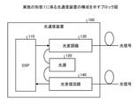
図1は、実施の形態1に係る光通信装置100の構成を示すブロック図である。図1に示す光通信装置100は、DSP(Digital Signal Processor)110、光源120、光変調器130及び光受信回路140を有する。
(Embodiment 1)
FIG. 1 is a block diagram showing a configuration of an optical communication device 100 according to a first embodiment. The optical communication device 100 shown in FIG. 1 includes a DSP (Digital Signal Processor) 110, a
DSP110は、デジタル信号処理を実行する電気部品である。具体的には、DSP110は、送信データの符号化などの処理を実行し、送信データを含む電気信号を生成して光変調器130へ出力する。また、DSP110は、受信データを含む電気信号を光受信回路140から取得し、電気信号の復号などの処理を実行して受信データを得る。
The DSP 110 is an electrical component that performs digital signal processing. Specifically, the DSP 110 executes processing such as encoding of transmission data, generates an electric signal including the transmission data, and outputs the electric signal to the
光源120は、例えばレーザダイオードなどを備え、所定の波長の光を発生させて光変調器130及び光受信回路140へ供給する。
The
光変調器130は、DSP110から出力される電気信号によって、光源120から供給される光を変調し、得られた光送信信号を光ファイバへ送出する。後述するように、光変調器130は、薄膜光導波路とマイクロストリップ構造の信号電極とを備え、光源120から供給される光が薄膜光導波路を伝搬する際に、この光を信号電極へ入力される電気信号によって変調し、光送信信号を生成する。光変調器130の構成については、後に詳述する。
The
光受信回路140は、光ファイバから光信号を受信し、光源120から供給される光を用いて受信光信号を復調する。そして、光受信回路140は、受信光信号を電気信号に変換し、得られた電気信号をDSP110へ出力する。
The
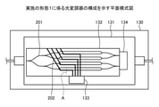
図2は、光変調器130の構成を示す平面模式図である。図2に示す光変調器130は、光変調器チップ131、光導波路基板132、RF(Radio Frequency:無線周波数)終端器133及びPBC(Polarization Beam Combiner:偏波ビームコンバイナ)134を有する。
FIG. 2 is a schematic plan view showing the configuration of the
光変調器チップ131は、入力側に光源120からの光ファイバが接続し、出力側に送信信号送出用の光ファイバが接続する半導体チップである。光変調器チップ131には、光導波路基板132、RF終端器133及びPBC134が実装される。
The
光導波路基板132は、薄膜光導波路201及び信号電極202を備え、光源120から供給される光が薄膜光導波路201を伝搬する際に、この光を信号電極202から印加される電界によって変調する。
The
薄膜光導波路201は、例えば薄膜LN基板を用いて形成される光導波路であり、光変調器チップ131の入力側から分岐を繰り返し、複数の平行な光導波路を有するマッハツェンダ干渉計を構成する。薄膜光導波路201を伝搬して変調された光は、PBC134へ出力される。
The thin film
信号電極202は、薄膜光導波路201に重なる位置に設けられるマイクロストリップ構造の伝送路であり、DSP110から出力される電気信号に応じて薄膜光導波路201へ電界を印加する。信号電極202の終端は、RF終端器133に接続されている。また、信号電極202は、露出する表面の少なくとも一部が誘電体によって被覆されており、信号電極202によって伝送されるマイクロ波の実効屈折率(等価屈折率)が大きくなっている。このため、信号電極202によって伝送されるマイクロ波の速度が低下し、薄膜光導波路201を伝搬する光の速度に近づく。これにより、高周波帯域での変調効率低下を抑制することができ、変調帯域を広帯域化することができる。
The
RF終端器133は、光導波路基板132上の信号電極202の終端に接続され、信号電極202によって伝送される信号の不要な反射を防止する。
The
PBC134は、光導波路基板132の出力側に配置され、薄膜光導波路201を伝搬して変調された光を偏波合成する。すなわち、PBC134は、光導波路基板132から出力される一組の光をそれぞれ例えば水平偏波及び垂直偏波として合成する。
The
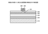
次に、光導波路基板132の構成について、具体的に説明する。図3は、図2の線分Aにおける断面を示す断面図である。
Next, the configuration of the
図3に示すように、薄膜光導波路201及び信号電極202の部分においては、LN基板210上にマイクロストリップ構造の接地電極220が積層され、接地電極220上にはバッファ層230、250に挟まれた薄膜LN基板240が積層される。
As shown in FIG. 3, in the thin film
LN基板210は、LN(ニオブ酸リチウム)からなる厚さが例えば数百μm程度の基板である。接地電極220は、例えば銅などの金属からなる厚さが例えば0.5~5μmの接地電位の電極である。バッファ層230は、例えばSiO2(二酸化ケイ素)又はTiO2(二酸化チタン)などの屈折率が高い透明材からなる厚さが1~10μmの層である。同様に、バッファ層250は、SiO2又はTiO2などからなる厚さが0.2~3μmの層である。
The
バッファ層230、250の間には、厚さが0.5~3μmの薄膜LN基板240が挟まれており、薄膜LN基板240の中央には、上方へ突起する薄膜光導波路201が形成される。薄膜光導波路201となる突起の幅は、例えば1~8μm程度である。薄膜LN基板240及び薄膜光導波路201は、バッファ層250によって被覆されており、バッファ層250の表面に信号電極202が配置される。つまり、信号電極202は、薄膜光導波路201を挟んで接地電極220に対向し、マイクロストリップ構造の伝送路を構成している。
A thin
信号電極202は、例えば銅などの金属からなり、幅が2~10μm、高さが1~20μmの電極である。DSP110から出力される電気信号に応じた高周波信号が信号電極202によって伝送されることにより、信号電極202から接地電極220へ向かう方向の電界が発生し、この電界が薄膜光導波路201に印加される。これにより、薄膜光導波路201の屈折率が変化し、薄膜光導波路201を伝搬する光を変調することが可能となる。
The
信号電極202の露出する側面及び上面は、誘電体膜260によって被覆される。誘電体膜260としては、例えばSiO2、TiO2、Al2O3(酸化アルミニウム)、Ta2O5(五酸化タンタル)などを成膜したものや、SiON膜(シリコン酸窒化膜)などを用いることができる。これらの誘電体を材料とする誘電体膜260を形成する際には、例えばスパッタ法などを用いた成膜をすることが可能である。誘電体膜260の膜厚は、例えば0.4~5μm程度である。
The exposed side and top surfaces of the
信号電極202の露出する表面が誘電体膜260によって被覆されることにより、信号電極202によって伝送されるマイクロ波の実効屈折率が大きくなる。実効屈折率の大きさは、誘電体膜260の膜厚を変化させることにより、所望の大きさに調節することが可能である。そして、実効屈折率が大きくなることによりマイクロ波の速度が低下し、薄膜光導波路201を伝搬する光の速度に近づく。結果として、高周波帯域での変調効率低下を抑制することができ、変調帯域を広帯域化することができる。
By covering the exposed surface of the
以上のように、本実施の形態によれば、マイクロストリップ構造の信号電極と接地電極の間に、薄膜光導波路が配置され、信号電極が誘電体膜によって被覆される。このため、信号電極によって伝送されるマイクロ波の実効屈折率が大きくなり、マイクロ波の速度が低下して薄膜光導波路を伝搬する光の速度に近づく。この結果、高周波帯域での変調効率低下を抑制することができ、変調帯域を広帯域化することができる。 As described above, according to the present embodiment, the thin film optical waveguide is arranged between the signal electrode of the microstrip structure and the ground electrode, and the signal electrode is covered with the dielectric film. Therefore, the effective refractive index of the microwave transmitted by the signal electrode increases, and the speed of the microwave decreases, approaching the speed of light propagating through the thin film optical waveguide. As a result, it is possible to suppress a decrease in modulation efficiency in the high frequency band, and it is possible to widen the modulation band.
なお、上述したように、誘電体膜260の膜厚を変化させることによって実効屈折率の大きさを調節することが可能であるため、信号電極202の大きさ(幅及び高さ)を比較的自由に変更することができる。
As described above, since the size of the effective refractive index can be adjusted by changing the film thickness of the
具体的には、例えば図4に示すように、信号電極202の幅WSを薄膜光導波路201の幅WLよりも大きくしても良い。こうすることにより、薄膜光導波路201への電界の印加効率をさらに向上することができ、駆動電圧を低減することが可能となる。また、信号電極202の幅WSを大きくすることで、信号電極202の断面積が大きくなって抵抗値が低下し、信号帯域を改善することができる。
Specifically, for example, as shown in FIG. 4, the width WS of the
また、例えば図5に示すように、信号電極202は、幅WSよりも高さHSが大きい断面形状を有しても良い。こうすることにより、信号電極202のインピーダンス低下を抑制して、高周波帯域の反射を抑制しつつ、信号電極202の断面積を大きくすることができる。
Further, for example, as shown in FIG. 5, the
(実施の形態2)
実施の形態2の特徴は、誘電体層に信号電極を埋設し、信号電極の側面を誘電体層によって被覆する点である。
(Embodiment 2)
The feature of the second embodiment is that the signal electrode is embedded in the dielectric layer and the side surface of the signal electrode is covered with the dielectric layer.
実施の形態2に係る光通信装置及び光変調器の構成は、実施の形態1と同様であるため、その説明を省略する。実施の形態2においては、光導波路基板132の構成が実施の形態1とは異なる。
Since the configurations of the optical communication device and the optical modulator according to the second embodiment are the same as those of the first embodiment, the description thereof will be omitted. In the second embodiment, the configuration of the
図6は、実施の形態2に係る光導波路基板132の構成を示す断面図である。図6は、図3と同様に、図2の線分Aにおける断面を示している。図6において、図3と同じ部分には同じ符号を付し、その説明を省略する。
FIG. 6 is a cross-sectional view showing the configuration of the
図6に示すように、実施の形態2においては、バッファ層250に誘電体層270が積層されている。そして、誘電体層270の薄膜光導波路201と重なる位置には開口部が形成され、開口部に信号電極202が配置される。このため、信号電極202の側面が誘電体層270によって被覆される一方、信号電極202の上面は露出している。
As shown in FIG. 6, in the second embodiment, the
誘電体層270としては、例えばSiO2、TiO2、Al2O3、Ta2O5などを成膜したものや、SiON膜を用いることができる。これらの誘電体を材料とする誘電体層270を形成する際には、例えばスパッタ法などを用いた成膜をすることが可能である。また、誘電体層270とバッファ層250が同一の材料からなる場合には、誘電体層270とバッファ層250を別体として設けなくても良く、誘電体層270とバッファ層250が一体化した誘電体層を設けても良い。
As the
誘電体層270の開口部は、例えばエッチング又はリフトオフによって薄膜光導波路201と重なる位置の誘電体が除去されることによって形成される。そして、例えば銅などの金属の蒸着及びめっきによって、誘電体層270の開口部に信号電極202が形成される。これにより、側面が誘電体層270によって被覆された信号電極202が形成される。このような形成方法によれば、信号電極202の側面及び上面に誘電体膜を成膜する必要がなく、光導波路基板132の製造工程を簡易にすることができる。
The opening of the
信号電極202の側面が誘電体層270によって被覆されることにより、信号電極202によって伝送されるマイクロ波の実効屈折率が大きくなる。実効屈折率の大きさは、信号電極202の幅方向における誘電体層270の厚さを変化させることにより、所望の大きさに調節することが可能である。信号電極202の幅方向における誘電体層270の厚さは、例えばエッチング又はリフトオフによって不要な部分を除去することにより変化させることができる。そして、実効屈折率が大きくなるとマイクロ波の速度が低下し、薄膜光導波路201を伝搬する光の速度に近づく。結果として、高周波帯域での変調効率低下を抑制することができ、変調帯域を広帯域化することができる。
By covering the side surface of the
以上のように、本実施の形態によれば、マイクロストリップ構造の信号電極と接地電極の間に、薄膜光導波路が配置され、誘電体層に埋設された信号電極の側面が誘電体層によって被覆される。このため、信号電極によって伝送されるマイクロ波の実効屈折率が大きくなり、マイクロ波の速度が低下して薄膜光導波路を伝搬する光の速度に近づく。この結果、高周波帯域での変調効率低下を抑制することができ、変調帯域を広帯域化することができる。また、誘電体に被覆される信号電極を容易に形成することができる。 As described above, according to the present embodiment, the thin film optical waveguide is arranged between the signal electrode of the microstrip structure and the ground electrode, and the side surface of the signal electrode embedded in the dielectric layer is covered with the dielectric layer. Will be done. Therefore, the effective refractive index of the microwave transmitted by the signal electrode increases, and the speed of the microwave decreases, approaching the speed of light propagating through the thin film optical waveguide. As a result, it is possible to suppress a decrease in modulation efficiency in the high frequency band, and it is possible to widen the modulation band. In addition, a signal electrode coated with a dielectric can be easily formed.
なお、上記実施の形態2において、信号電極202の断面積を大きくして抵抗値を低下させるために、例えば図7に示すように、信号電極202の上面に追加電極203を接続しても良い。このとき、追加電極203の幅W2を信号電極202の幅W1よりも大きくして、効率的に断面積を増大させても良い。すなわち、追加電極203は、信号電極202の上面から誘電体層270の上面にまで広がって形成されても良い。
In the second embodiment, in order to increase the cross-sectional area of the
追加電極203は、例えば誘電体層270の上面に幅W2の開口部を有するレジストを形成し、この開口部に例えば銅などの金属を蒸着及びめっきすることにより形成される。このとき、信号電極202とは別工程で追加電極203を形成しても良いが、誘電体層270に信号電極202のための開口部を形成した後、誘電体層270の上面にレジストを形成して蒸着及びめっきを行うことにより、信号電極202及び追加電極203が一体となった電極を同時に形成しても良い。
The
なお、上記実施の形態2においては、信号電極202の高さと誘電体層270の厚さが一致するものとしたが、必ずしも信号電極202の高さと誘電体層270の厚さが一致していなくても良い。すなわち、例えば信号電極202の高さよりも誘電体層270の厚さが小さく、信号電極202の側面のバッファ層250に近い部分のみが誘電体層270に被覆されるようにしても良い。信号電極202から発生する電界は、接地電極220に近い下方ほど大きくなるため、信号電極202の側面のバッファ層250に近い下方が誘電体層270によって被覆されることにより、効率的に実効屈折率を大きくすることができる。
In the second embodiment, the height of the
110 DSP
120 光源
130 光変調器
131 光変調器チップ
132 光導波路基板
133 RF終端器
134 PBC
140 光受信回路
201 薄膜光導波路
202 信号電極
203 追加電極
210 LN基板
220 接地電極
230、250 バッファ層
240 薄膜LN基板
260 誘電体膜
270 誘電体層
110 DSP
120
140
Claims (8)
前記接地電極に積層される薄膜基板によって形成される薄膜光導波路と、
前記薄膜光導波路を挟んで前記接地電極と対向する位置に配置され、高周波信号を伝送する信号電極と、
前記信号電極の露出する表面の少なくとも一部を被覆する誘電体と
を有することを特徴とする光デバイス。 The ground electrode of the ground potential and
A thin-film optical waveguide formed by a thin-film substrate laminated on the ground electrode,
A signal electrode arranged at a position facing the ground electrode across the thin film optical waveguide and transmitting a high frequency signal, and a signal electrode.
An optical device comprising a dielectric that covers at least a portion of the exposed surface of the signal electrode.
前記薄膜基板に積層され、前記薄膜光導波路を被覆する第2のバッファ層とをさらに有し、
前記信号電極は、
前記第2のバッファ層の表面の前記薄膜光導波路と重なる位置に配置される
ことを特徴とする請求項1記載の光デバイス。 A first buffer layer laminated between the ground electrode and the thin film substrate,
It further has a second buffer layer laminated on the thin film substrate and covering the thin film optical waveguide.
The signal electrode is
The optical device according to claim 1, wherein the optical device is arranged at a position overlapping the thin film optical waveguide on the surface of the second buffer layer.
前記薄膜光導波路の幅よりも大きい幅を有する
ことを特徴とする請求項1記載の光デバイス。 The signal electrode is
The optical device according to claim 1, wherein the optical device has a width larger than the width of the thin film optical waveguide.
幅よりも高さが大きい断面形状を有する
ことを特徴とする請求項1記載の光デバイス。 The signal electrode is
The optical device according to claim 1, wherein the optical device has a cross-sectional shape having a height larger than a width.
前記信号電極の側面と前記接地電極から遠い側の面とを被覆する誘電体膜を備える
ことを特徴とする請求項1記載の光デバイス。 The dielectric is
The optical device according to claim 1, further comprising a dielectric film that covers a side surface of the signal electrode and a surface far from the ground electrode.
前記薄膜基板に積層される誘電体層を備え、
前記信号電極は、
前記誘電体層の前記薄膜光導波路と重なる位置に埋設される
ことを特徴とする請求項1記載の光デバイス。 The dielectric is
A dielectric layer laminated on the thin film substrate is provided.
The signal electrode is
The optical device according to claim 1, wherein the dielectric layer is embedded at a position overlapping with the thin film optical waveguide.
側面が前記誘電体によって被覆された第1の電極と、
前記第1の電極の前記接地電極から遠い側の面に接続し、前記第1の電極よりも幅広の第2の電極と
を有することを特徴とする請求項1記載の光デバイス。 The signal electrode is
A first electrode whose side surface is coated with the dielectric,
The optical device according to claim 1, wherein the first electrode is connected to a surface on the side far from the ground electrode and has a second electrode wider than the first electrode.
光を発生させる光源と、
前記プロセッサから出力される電気信号を用いて、前記光源から発生する光を変調する光デバイスとを有し、
前記光デバイスは、
接地電位の接地電極と、
前記接地電極に積層される薄膜基板によって形成される薄膜光導波路と、
前記薄膜光導波路を挟んで前記接地電極と対向する位置に配置され、高周波信号を伝送する信号電極と、
前記信号電極の露出する表面の少なくとも一部を被覆する誘電体とを有する
ことを特徴とする光通信装置。 A processor that performs signal processing on electrical signals and
A light source that generates light,
It has an optical device that modulates the light generated from the light source by using an electric signal output from the processor.
The optical device is
The ground electrode of the ground potential and
A thin-film optical waveguide formed by a thin-film substrate laminated on the ground electrode,
A signal electrode arranged at a position facing the ground electrode across the thin film optical waveguide and transmitting a high frequency signal, and a signal electrode.
An optical communication device comprising a dielectric covering at least a part of an exposed surface of the signal electrode.
Priority Applications (3)
| Application Number | Priority Date | Filing Date | Title |
|---|---|---|---|
| JP2020115650A JP2022013232A (en) | 2020-07-03 | 2020-07-03 | Optical device and optical communication apparatus |
| CN202110582615.XA CN113885227A (en) | 2020-07-03 | 2021-05-27 | Optical device and optical communication apparatus |
| US17/334,040 US11719964B2 (en) | 2020-07-03 | 2021-05-28 | Optical device and optical communication device |
Applications Claiming Priority (1)
| Application Number | Priority Date | Filing Date | Title |
|---|---|---|---|
| JP2020115650A JP2022013232A (en) | 2020-07-03 | 2020-07-03 | Optical device and optical communication apparatus |
Publications (1)
| Publication Number | Publication Date |
|---|---|
| JP2022013232A true JP2022013232A (en) | 2022-01-18 |
Family
ID=79010106
Family Applications (1)
| Application Number | Title | Priority Date | Filing Date |
|---|---|---|---|
| JP2020115650A Pending JP2022013232A (en) | 2020-07-03 | 2020-07-03 | Optical device and optical communication apparatus |
Country Status (3)
| Country | Link |
|---|---|
| US (1) | US11719964B2 (en) |
| JP (1) | JP2022013232A (en) |
| CN (1) | CN113885227A (en) |
Cited By (1)
| Publication number | Priority date | Publication date | Assignee | Title |
|---|---|---|---|---|
| WO2023188195A1 (en) * | 2022-03-30 | 2023-10-05 | 住友大阪セメント株式会社 | Optical waveguide element, optical modulation device using same, and optical transmission device |
Families Citing this family (1)
| Publication number | Priority date | Publication date | Assignee | Title |
|---|---|---|---|---|
| JP2022013232A (en) * | 2020-07-03 | 2022-01-18 | 富士通オプティカルコンポーネンツ株式会社 | Optical device and optical communication apparatus |
Family Cites Families (13)
| Publication number | Priority date | Publication date | Assignee | Title |
|---|---|---|---|---|
| JP3021888B2 (en) * | 1991-12-04 | 2000-03-15 | 住友金属鉱山株式会社 | Optical waveguide functional element and method of manufacturing the same |
| JPH0954293A (en) * | 1995-08-17 | 1997-02-25 | Sony Corp | Optical waveguide element |
| JP2836568B2 (en) * | 1996-02-19 | 1998-12-14 | 日本電気株式会社 | Light control element and method of manufacturing the same |
| US6310700B1 (en) | 2000-09-15 | 2001-10-30 | Massachusetts Institute Of Technology | Velocity matching electrode structure for electro-optic modulators |
| JP2004227013A (en) * | 2000-12-22 | 2004-08-12 | Nec Corp | Optical waveguide device and its manufacturing method |
| JP2009098196A (en) * | 2007-10-12 | 2009-05-07 | Fuji Xerox Co Ltd | Optical waveguide device and polling processing method of optical waveguide device |
| US8224143B2 (en) * | 2010-02-05 | 2012-07-17 | Advantest Corporation | Substrate structure and manufacturing method |
| JP5792702B2 (en) | 2012-09-26 | 2015-10-14 | 住友大阪セメント株式会社 | Light modulator |
| JP6221294B2 (en) | 2013-03-28 | 2017-11-01 | 住友大阪セメント株式会社 | Light control element |
| CN105829957A (en) * | 2013-12-11 | 2016-08-03 | 住友大阪水泥股份有限公司 | Electro-optical element |
| JP5983839B2 (en) | 2015-08-06 | 2016-09-06 | 住友大阪セメント株式会社 | Light modulator |
| JP6561383B2 (en) * | 2017-03-31 | 2019-08-21 | 住友大阪セメント株式会社 | Light modulation element |
| JP2022013232A (en) * | 2020-07-03 | 2022-01-18 | 富士通オプティカルコンポーネンツ株式会社 | Optical device and optical communication apparatus |
-
2020
- 2020-07-03 JP JP2020115650A patent/JP2022013232A/en active Pending
-
2021
- 2021-05-27 CN CN202110582615.XA patent/CN113885227A/en active Pending
- 2021-05-28 US US17/334,040 patent/US11719964B2/en active Active
Cited By (1)
| Publication number | Priority date | Publication date | Assignee | Title |
|---|---|---|---|---|
| WO2023188195A1 (en) * | 2022-03-30 | 2023-10-05 | 住友大阪セメント株式会社 | Optical waveguide element, optical modulation device using same, and optical transmission device |
Also Published As
| Publication number | Publication date |
|---|---|
| US20220004031A1 (en) | 2022-01-06 |
| CN113885227A (en) | 2022-01-04 |
| US11719964B2 (en) | 2023-08-08 |
Similar Documents
| Publication | Publication Date | Title |
|---|---|---|
| US7912326B2 (en) | Optical control device | |
| US10228605B2 (en) | Waveguide optical element | |
| WO2007007604A1 (en) | Optical modulator | |
| US9235066B2 (en) | Optical modulator | |
| US11719964B2 (en) | Optical device and optical communication device | |
| US20220163827A1 (en) | Optical device, optical communication apparatus, and manufacturing method of the optical device | |
| WO2008108154A1 (en) | Optical phase modulator | |
| JP2004163859A (en) | Optical modulator | |
| US6646776B1 (en) | Suppression of high frequency resonance in an electro-optical modulator | |
| WO2020170871A1 (en) | Optical modulator | |
| US6768570B2 (en) | Optical modulator | |
| US6885780B2 (en) | Suppression of high frequency resonance in an electro-optical modulator | |
| CN115079446A (en) | Optical device, optical communication device, and method of manufacturing optical device | |
| US20230258967A1 (en) | Optical waveguide device, optical modulator, optical modulation module, and optical transmission apparatus | |
| US20220082876A1 (en) | Optical device that includes optical modulator, and optical transceiver | |
| JP2919132B2 (en) | Light modulator | |
| JP2021179569A (en) | Optical device and optical transmitter-receiver using the same | |
| JP2021026090A (en) | Optical device | |
| JP2004245991A (en) | Optical waveguide device and structure combining the same and optical transmission member | |
| US11320715B2 (en) | Optical device that includes optical modulator | |
| JP2010032690A (en) | Optical modulator | |
| JP2010044197A (en) | Light modulator | |
| JP2022189553A (en) | Optical device and optical communication device | |
| JP6394243B2 (en) | Optical waveguide device | |
| JP2022189578A (en) | Optical device and optical communication device |
Legal Events
| Date | Code | Title | Description |
|---|---|---|---|
| A621 | Written request for application examination |
Free format text: JAPANESE INTERMEDIATE CODE: A621 Effective date: 20230403 |
|
| A977 | Report on retrieval |
Free format text: JAPANESE INTERMEDIATE CODE: A971007 Effective date: 20231129 |
|
| A131 | Notification of reasons for refusal |
Free format text: JAPANESE INTERMEDIATE CODE: A131 Effective date: 20231205 |
|
| A521 | Request for written amendment filed |
Free format text: JAPANESE INTERMEDIATE CODE: A523 Effective date: 20240201 |
|
| A02 | Decision of refusal |
Free format text: JAPANESE INTERMEDIATE CODE: A02 Effective date: 20240416 |