JP2021523332A - Electrode structure for microvalves for use in injection assemblies - Google Patents
Electrode structure for microvalves for use in injection assemblies Download PDFInfo
- Publication number
- JP2021523332A JP2021523332A JP2020563601A JP2020563601A JP2021523332A JP 2021523332 A JP2021523332 A JP 2021523332A JP 2020563601 A JP2020563601 A JP 2020563601A JP 2020563601 A JP2020563601 A JP 2020563601A JP 2021523332 A JP2021523332 A JP 2021523332A
- Authority
- JP
- Japan
- Prior art keywords
- layer
- electrode layer
- working beam
- electrical connection
- piezoelectric material
- Prior art date
- Legal status (The legal status is an assumption and is not a legal conclusion. Google has not performed a legal analysis and makes no representation as to the accuracy of the status listed.)
- Pending
Links
- 238000002347 injection Methods 0.000 title claims description 62
- 239000007924 injection Substances 0.000 title claims description 62
- 230000000712 assembly Effects 0.000 title description 2
- 238000000429 assembly Methods 0.000 title description 2
- 239000000463 material Substances 0.000 claims abstract description 139
- 230000004044 response Effects 0.000 claims abstract description 22
- 239000012530 fluid Substances 0.000 claims description 211
- 238000007789 sealing Methods 0.000 claims description 73
- 238000002161 passivation Methods 0.000 claims description 50
- 230000004888 barrier function Effects 0.000 claims description 36
- 125000006850 spacer group Chemical group 0.000 claims description 30
- 238000004891 communication Methods 0.000 claims description 5
- 238000010586 diagram Methods 0.000 abstract description 3
- 239000010410 layer Substances 0.000 description 506
- 239000000853 adhesive Substances 0.000 description 35
- 230000001070 adhesive effect Effects 0.000 description 35
- 239000012790 adhesive layer Substances 0.000 description 35
- VYPSYNLAJGMNEJ-UHFFFAOYSA-N Silicium dioxide Chemical compound O=[Si]=O VYPSYNLAJGMNEJ-UHFFFAOYSA-N 0.000 description 34
- XUIMIQQOPSSXEZ-UHFFFAOYSA-N Silicon Chemical compound [Si] XUIMIQQOPSSXEZ-UHFFFAOYSA-N 0.000 description 16
- 238000000034 method Methods 0.000 description 16
- 229910052710 silicon Inorganic materials 0.000 description 16
- 239000010703 silicon Substances 0.000 description 16
- 239000000377 silicon dioxide Substances 0.000 description 16
- 230000006870 function Effects 0.000 description 15
- 235000012239 silicon dioxide Nutrition 0.000 description 13
- 238000000151 deposition Methods 0.000 description 11
- 239000011521 glass Substances 0.000 description 11
- 229920001486 SU-8 photoresist Polymers 0.000 description 10
- 229910052751 metal Inorganic materials 0.000 description 10
- 239000002184 metal Substances 0.000 description 10
- BASFCYQUMIYNBI-UHFFFAOYSA-N platinum Chemical compound [Pt] BASFCYQUMIYNBI-UHFFFAOYSA-N 0.000 description 10
- PCHJSUWPFVWCPO-UHFFFAOYSA-N gold Chemical compound [Au] PCHJSUWPFVWCPO-UHFFFAOYSA-N 0.000 description 9
- 229910052737 gold Inorganic materials 0.000 description 9
- 239000010931 gold Substances 0.000 description 9
- 230000007797 corrosion Effects 0.000 description 8
- 238000005260 corrosion Methods 0.000 description 8
- 230000008021 deposition Effects 0.000 description 8
- 239000008393 encapsulating agent Substances 0.000 description 8
- 238000012986 modification Methods 0.000 description 8
- 230000004048 modification Effects 0.000 description 8
- 229920001296 polysiloxane Polymers 0.000 description 8
- 230000008569 process Effects 0.000 description 8
- 238000000926 separation method Methods 0.000 description 8
- 238000013461 design Methods 0.000 description 7
- 238000003780 insertion Methods 0.000 description 7
- 230000037431 insertion Effects 0.000 description 7
- 239000012212 insulator Substances 0.000 description 7
- 238000003860 storage Methods 0.000 description 7
- 229920006362 Teflon® Polymers 0.000 description 6
- 229910052451 lead zirconate titanate Inorganic materials 0.000 description 6
- TWNQGVIAIRXVLR-UHFFFAOYSA-N oxo(oxoalumanyloxy)alumane Chemical compound O=[Al]O[Al]=O TWNQGVIAIRXVLR-UHFFFAOYSA-N 0.000 description 6
- 235000012431 wafers Nutrition 0.000 description 6
- 229910052581 Si3N4 Inorganic materials 0.000 description 5
- 238000005452 bending Methods 0.000 description 5
- 230000015572 biosynthetic process Effects 0.000 description 5
- 238000000576 coating method Methods 0.000 description 5
- 229910052697 platinum Inorganic materials 0.000 description 5
- HQVNEWCFYHHQES-UHFFFAOYSA-N silicon nitride Chemical compound N12[Si]34N5[Si]62N3[Si]51N64 HQVNEWCFYHHQES-UHFFFAOYSA-N 0.000 description 5
- 229910001220 stainless steel Inorganic materials 0.000 description 5
- 239000010935 stainless steel Substances 0.000 description 5
- PXHVJJICTQNCMI-UHFFFAOYSA-N Nickel Chemical compound [Ni] PXHVJJICTQNCMI-UHFFFAOYSA-N 0.000 description 4
- KDLHZDBZIXYQEI-UHFFFAOYSA-N Palladium Chemical compound [Pd] KDLHZDBZIXYQEI-UHFFFAOYSA-N 0.000 description 4
- 239000000919 ceramic Substances 0.000 description 4
- 239000000470 constituent Substances 0.000 description 4
- 230000008878 coupling Effects 0.000 description 4
- 238000010168 coupling process Methods 0.000 description 4
- 238000005859 coupling reaction Methods 0.000 description 4
- 238000005530 etching Methods 0.000 description 4
- 238000010438 heat treatment Methods 0.000 description 4
- 238000004519 manufacturing process Methods 0.000 description 4
- 239000004033 plastic Substances 0.000 description 4
- 229920003023 plastic Polymers 0.000 description 4
- 229920003229 poly(methyl methacrylate) Polymers 0.000 description 4
- 239000004926 polymethyl methacrylate Substances 0.000 description 4
- 229910052701 rubidium Inorganic materials 0.000 description 4
- IGLNJRXAVVLDKE-UHFFFAOYSA-N rubidium atom Chemical compound [Rb] IGLNJRXAVVLDKE-UHFFFAOYSA-N 0.000 description 4
- 229920002379 silicone rubber Polymers 0.000 description 4
- 239000004945 silicone rubber Substances 0.000 description 4
- GWEVSGVZZGPLCZ-UHFFFAOYSA-N Titan oxide Chemical compound O=[Ti]=O GWEVSGVZZGPLCZ-UHFFFAOYSA-N 0.000 description 3
- RTAQQCXQSZGOHL-UHFFFAOYSA-N Titanium Chemical compound [Ti] RTAQQCXQSZGOHL-UHFFFAOYSA-N 0.000 description 3
- 239000011248 coating agent Substances 0.000 description 3
- 230000006378 damage Effects 0.000 description 3
- 238000009792 diffusion process Methods 0.000 description 3
- 230000000694 effects Effects 0.000 description 3
- 230000002209 hydrophobic effect Effects 0.000 description 3
- HFGPZNIAWCZYJU-UHFFFAOYSA-N lead zirconate titanate Chemical compound [O-2].[O-2].[O-2].[O-2].[O-2].[Ti+4].[Zr+4].[Pb+2] HFGPZNIAWCZYJU-UHFFFAOYSA-N 0.000 description 3
- 230000002093 peripheral effect Effects 0.000 description 3
- 229920002120 photoresistant polymer Polymers 0.000 description 3
- 229920000052 poly(p-xylylene) Polymers 0.000 description 3
- 239000000126 substance Substances 0.000 description 3
- 238000006467 substitution reaction Methods 0.000 description 3
- 239000000758 substrate Substances 0.000 description 3
- 239000010936 titanium Substances 0.000 description 3
- 229910052719 titanium Inorganic materials 0.000 description 3
- IJGRMHOSHXDMSA-UHFFFAOYSA-N Atomic nitrogen Chemical compound N#N IJGRMHOSHXDMSA-UHFFFAOYSA-N 0.000 description 2
- 239000004593 Epoxy Substances 0.000 description 2
- 241001542009 Talinum Species 0.000 description 2
- XLOMVQKBTHCTTD-UHFFFAOYSA-N Zinc monoxide Chemical compound [Zn]=O XLOMVQKBTHCTTD-UHFFFAOYSA-N 0.000 description 2
- 230000004913 activation Effects 0.000 description 2
- IISBACLAFKSPIT-UHFFFAOYSA-N bisphenol A Chemical compound C=1C=C(O)C=CC=1C(C)(C)C1=CC=C(O)C=C1 IISBACLAFKSPIT-UHFFFAOYSA-N 0.000 description 2
- 230000015556 catabolic process Effects 0.000 description 2
- 238000013016 damping Methods 0.000 description 2
- 230000007547 defect Effects 0.000 description 2
- 238000006731 degradation reaction Methods 0.000 description 2
- 238000005137 deposition process Methods 0.000 description 2
- 230000006866 deterioration Effects 0.000 description 2
- 230000001627 detrimental effect Effects 0.000 description 2
- 239000004205 dimethyl polysiloxane Substances 0.000 description 2
- 229920001971 elastomer Polymers 0.000 description 2
- 229920006332 epoxy adhesive Polymers 0.000 description 2
- 238000001704 evaporation Methods 0.000 description 2
- 230000008020 evaporation Effects 0.000 description 2
- 150000002500 ions Chemical class 0.000 description 2
- 239000007788 liquid Substances 0.000 description 2
- 238000012423 maintenance Methods 0.000 description 2
- 230000005012 migration Effects 0.000 description 2
- 238000013508 migration Methods 0.000 description 2
- 230000007935 neutral effect Effects 0.000 description 2
- 229910052759 nickel Inorganic materials 0.000 description 2
- 230000003647 oxidation Effects 0.000 description 2
- 238000007254 oxidation reaction Methods 0.000 description 2
- RVTZCBVAJQQJTK-UHFFFAOYSA-N oxygen(2-);zirconium(4+) Chemical compound [O-2].[O-2].[Zr+4] RVTZCBVAJQQJTK-UHFFFAOYSA-N 0.000 description 2
- 229910052763 palladium Inorganic materials 0.000 description 2
- 239000002245 particle Substances 0.000 description 2
- 230000000737 periodic effect Effects 0.000 description 2
- 229920000435 poly(dimethylsiloxane) Polymers 0.000 description 2
- -1 polydimethylsiloxane Polymers 0.000 description 2
- 230000001681 protective effect Effects 0.000 description 2
- 229910052814 silicon oxide Inorganic materials 0.000 description 2
- 229910052715 tantalum Inorganic materials 0.000 description 2
- GUVRBAGPIYLISA-UHFFFAOYSA-N tantalum atom Chemical compound [Ta] GUVRBAGPIYLISA-UHFFFAOYSA-N 0.000 description 2
- 238000001947 vapour-phase growth Methods 0.000 description 2
- XLYOFNOQVPJJNP-UHFFFAOYSA-N water Substances O XLYOFNOQVPJJNP-UHFFFAOYSA-N 0.000 description 2
- ZEMPKEQAKRGZGQ-AAKVHIHISA-N 2,3-bis[[(z)-12-hydroxyoctadec-9-enoyl]oxy]propyl (z)-12-hydroxyoctadec-9-enoate Chemical compound CCCCCCC(O)C\C=C/CCCCCCCC(=O)OCC(OC(=O)CCCCCCC\C=C/CC(O)CCCCCC)COC(=O)CCCCCCC\C=C/CC(O)CCCCCC ZEMPKEQAKRGZGQ-AAKVHIHISA-N 0.000 description 1
- 239000004642 Polyimide Substances 0.000 description 1
- MCMNRKCIXSYSNV-UHFFFAOYSA-N ZrO2 Inorganic materials O=[Zr]=O MCMNRKCIXSYSNV-UHFFFAOYSA-N 0.000 description 1
- 230000002411 adverse Effects 0.000 description 1
- 239000003570 air Substances 0.000 description 1
- QVGXLLKOCUKJST-UHFFFAOYSA-N atomic oxygen Chemical compound [O] QVGXLLKOCUKJST-UHFFFAOYSA-N 0.000 description 1
- 230000009286 beneficial effect Effects 0.000 description 1
- 230000008901 benefit Effects 0.000 description 1
- 230000008859 change Effects 0.000 description 1
- 238000003486 chemical etching Methods 0.000 description 1
- 239000003086 colorant Substances 0.000 description 1
- 230000006835 compression Effects 0.000 description 1
- 238000007906 compression Methods 0.000 description 1
- 239000004020 conductor Substances 0.000 description 1
- 238000011109 contamination Methods 0.000 description 1
- 239000013078 crystal Substances 0.000 description 1
- 238000005520 cutting process Methods 0.000 description 1
- 238000000708 deep reactive-ion etching Methods 0.000 description 1
- GYZLOYUZLJXAJU-UHFFFAOYSA-N diglycidyl ether Chemical compound C1OC1COCC1CO1 GYZLOYUZLJXAJU-UHFFFAOYSA-N 0.000 description 1
- NKZSPGSOXYXWQA-UHFFFAOYSA-N dioxido(oxo)titanium;lead(2+) Chemical compound [Pb+2].[O-][Ti]([O-])=O NKZSPGSOXYXWQA-UHFFFAOYSA-N 0.000 description 1
- 238000005553 drilling Methods 0.000 description 1
- 238000001312 dry etching Methods 0.000 description 1
- 230000009977 dual effect Effects 0.000 description 1
- 238000005566 electron beam evaporation Methods 0.000 description 1
- 238000005516 engineering process Methods 0.000 description 1
- 239000006260 foam Substances 0.000 description 1
- 230000004927 fusion Effects 0.000 description 1
- 239000007789 gas Substances 0.000 description 1
- 230000007774 longterm Effects 0.000 description 1
- 230000007246 mechanism Effects 0.000 description 1
- 238000002156 mixing Methods 0.000 description 1
- 239000002105 nanoparticle Substances 0.000 description 1
- 229910052757 nitrogen Inorganic materials 0.000 description 1
- 239000001301 oxygen Substances 0.000 description 1
- 229910052760 oxygen Inorganic materials 0.000 description 1
- 238000012856 packing Methods 0.000 description 1
- 238000005192 partition Methods 0.000 description 1
- 238000000206 photolithography Methods 0.000 description 1
- 229920001721 polyimide Polymers 0.000 description 1
- 229920000642 polymer Polymers 0.000 description 1
- 238000007639 printing Methods 0.000 description 1
- 230000008439 repair process Effects 0.000 description 1
- 230000006903 response to temperature Effects 0.000 description 1
- 238000005488 sandblasting Methods 0.000 description 1
- 230000008054 signal transmission Effects 0.000 description 1
- 239000002356 single layer Substances 0.000 description 1
- 229910000679 solder Inorganic materials 0.000 description 1
- 238000004544 sputter deposition Methods 0.000 description 1
- 238000002207 thermal evaporation Methods 0.000 description 1
- 239000004408 titanium dioxide Substances 0.000 description 1
- OGIDPMRJRNCKJF-UHFFFAOYSA-N titanium oxide Inorganic materials [Ti]=O OGIDPMRJRNCKJF-UHFFFAOYSA-N 0.000 description 1
- 238000001771 vacuum deposition Methods 0.000 description 1
- 238000001039 wet etching Methods 0.000 description 1
- 239000011787 zinc oxide Substances 0.000 description 1
- 229910001928 zirconium oxide Inorganic materials 0.000 description 1
Images


Classifications
-
- B—PERFORMING OPERATIONS; TRANSPORTING
- B41—PRINTING; LINING MACHINES; TYPEWRITERS; STAMPS
- B41J—TYPEWRITERS; SELECTIVE PRINTING MECHANISMS, i.e. MECHANISMS PRINTING OTHERWISE THAN FROM A FORME; CORRECTION OF TYPOGRAPHICAL ERRORS
- B41J2/00—Typewriters or selective printing mechanisms characterised by the printing or marking process for which they are designed
- B41J2/005—Typewriters or selective printing mechanisms characterised by the printing or marking process for which they are designed characterised by bringing liquid or particles selectively into contact with a printing material
- B41J2/01—Ink jet
- B41J2/135—Nozzles
- B41J2/14—Structure thereof only for on-demand ink jet heads
- B41J2/14201—Structure of print heads with piezoelectric elements
- B41J2/14282—Structure of print heads with piezoelectric elements of cantilever type
-
- B—PERFORMING OPERATIONS; TRANSPORTING
- B41—PRINTING; LINING MACHINES; TYPEWRITERS; STAMPS
- B41J—TYPEWRITERS; SELECTIVE PRINTING MECHANISMS, i.e. MECHANISMS PRINTING OTHERWISE THAN FROM A FORME; CORRECTION OF TYPOGRAPHICAL ERRORS
- B41J2/00—Typewriters or selective printing mechanisms characterised by the printing or marking process for which they are designed
- B41J2/005—Typewriters or selective printing mechanisms characterised by the printing or marking process for which they are designed characterised by bringing liquid or particles selectively into contact with a printing material
- B41J2/01—Ink jet
- B41J2/135—Nozzles
- B41J2/14—Structure thereof only for on-demand ink jet heads
- B41J2/14201—Structure of print heads with piezoelectric elements
-
- B—PERFORMING OPERATIONS; TRANSPORTING
- B41—PRINTING; LINING MACHINES; TYPEWRITERS; STAMPS
- B41J—TYPEWRITERS; SELECTIVE PRINTING MECHANISMS, i.e. MECHANISMS PRINTING OTHERWISE THAN FROM A FORME; CORRECTION OF TYPOGRAPHICAL ERRORS
- B41J2/00—Typewriters or selective printing mechanisms characterised by the printing or marking process for which they are designed
- B41J2/005—Typewriters or selective printing mechanisms characterised by the printing or marking process for which they are designed characterised by bringing liquid or particles selectively into contact with a printing material
- B41J2/01—Ink jet
- B41J2/135—Nozzles
- B41J2/16—Production of nozzles
- B41J2/1607—Production of print heads with piezoelectric elements
- B41J2/1614—Production of print heads with piezoelectric elements of cantilever type
-
- B—PERFORMING OPERATIONS; TRANSPORTING
- B41—PRINTING; LINING MACHINES; TYPEWRITERS; STAMPS
- B41J—TYPEWRITERS; SELECTIVE PRINTING MECHANISMS, i.e. MECHANISMS PRINTING OTHERWISE THAN FROM A FORME; CORRECTION OF TYPOGRAPHICAL ERRORS
- B41J2/00—Typewriters or selective printing mechanisms characterised by the printing or marking process for which they are designed
- B41J2/005—Typewriters or selective printing mechanisms characterised by the printing or marking process for which they are designed characterised by bringing liquid or particles selectively into contact with a printing material
- B41J2/01—Ink jet
- B41J2/135—Nozzles
- B41J2/16—Production of nozzles
- B41J2/1621—Manufacturing processes
- B41J2/1623—Manufacturing processes bonding and adhesion
-
- B—PERFORMING OPERATIONS; TRANSPORTING
- B41—PRINTING; LINING MACHINES; TYPEWRITERS; STAMPS
- B41J—TYPEWRITERS; SELECTIVE PRINTING MECHANISMS, i.e. MECHANISMS PRINTING OTHERWISE THAN FROM A FORME; CORRECTION OF TYPOGRAPHICAL ERRORS
- B41J2/00—Typewriters or selective printing mechanisms characterised by the printing or marking process for which they are designed
- B41J2/005—Typewriters or selective printing mechanisms characterised by the printing or marking process for which they are designed characterised by bringing liquid or particles selectively into contact with a printing material
- B41J2/01—Ink jet
- B41J2/135—Nozzles
- B41J2/16—Production of nozzles
- B41J2/1621—Manufacturing processes
- B41J2/1626—Manufacturing processes etching
- B41J2/1628—Manufacturing processes etching dry etching
-
- B—PERFORMING OPERATIONS; TRANSPORTING
- B41—PRINTING; LINING MACHINES; TYPEWRITERS; STAMPS
- B41J—TYPEWRITERS; SELECTIVE PRINTING MECHANISMS, i.e. MECHANISMS PRINTING OTHERWISE THAN FROM A FORME; CORRECTION OF TYPOGRAPHICAL ERRORS
- B41J2/00—Typewriters or selective printing mechanisms characterised by the printing or marking process for which they are designed
- B41J2/005—Typewriters or selective printing mechanisms characterised by the printing or marking process for which they are designed characterised by bringing liquid or particles selectively into contact with a printing material
- B41J2/01—Ink jet
- B41J2/135—Nozzles
- B41J2/16—Production of nozzles
- B41J2/1621—Manufacturing processes
- B41J2/1626—Manufacturing processes etching
- B41J2/1629—Manufacturing processes etching wet etching
-
- B—PERFORMING OPERATIONS; TRANSPORTING
- B41—PRINTING; LINING MACHINES; TYPEWRITERS; STAMPS
- B41J—TYPEWRITERS; SELECTIVE PRINTING MECHANISMS, i.e. MECHANISMS PRINTING OTHERWISE THAN FROM A FORME; CORRECTION OF TYPOGRAPHICAL ERRORS
- B41J2/00—Typewriters or selective printing mechanisms characterised by the printing or marking process for which they are designed
- B41J2/005—Typewriters or selective printing mechanisms characterised by the printing or marking process for which they are designed characterised by bringing liquid or particles selectively into contact with a printing material
- B41J2/01—Ink jet
- B41J2/135—Nozzles
- B41J2/16—Production of nozzles
- B41J2/1621—Manufacturing processes
- B41J2/1631—Manufacturing processes photolithography
-
- B—PERFORMING OPERATIONS; TRANSPORTING
- B41—PRINTING; LINING MACHINES; TYPEWRITERS; STAMPS
- B41J—TYPEWRITERS; SELECTIVE PRINTING MECHANISMS, i.e. MECHANISMS PRINTING OTHERWISE THAN FROM A FORME; CORRECTION OF TYPOGRAPHICAL ERRORS
- B41J2/00—Typewriters or selective printing mechanisms characterised by the printing or marking process for which they are designed
- B41J2/005—Typewriters or selective printing mechanisms characterised by the printing or marking process for which they are designed characterised by bringing liquid or particles selectively into contact with a printing material
- B41J2/01—Ink jet
- B41J2/135—Nozzles
- B41J2/16—Production of nozzles
- B41J2/1621—Manufacturing processes
- B41J2/1632—Manufacturing processes machining
-
- B—PERFORMING OPERATIONS; TRANSPORTING
- B41—PRINTING; LINING MACHINES; TYPEWRITERS; STAMPS
- B41J—TYPEWRITERS; SELECTIVE PRINTING MECHANISMS, i.e. MECHANISMS PRINTING OTHERWISE THAN FROM A FORME; CORRECTION OF TYPOGRAPHICAL ERRORS
- B41J2/00—Typewriters or selective printing mechanisms characterised by the printing or marking process for which they are designed
- B41J2/005—Typewriters or selective printing mechanisms characterised by the printing or marking process for which they are designed characterised by bringing liquid or particles selectively into contact with a printing material
- B41J2/01—Ink jet
- B41J2/135—Nozzles
- B41J2/16—Production of nozzles
- B41J2/1621—Manufacturing processes
- B41J2/164—Manufacturing processes thin film formation
-
- F—MECHANICAL ENGINEERING; LIGHTING; HEATING; WEAPONS; BLASTING
- F16—ENGINEERING ELEMENTS AND UNITS; GENERAL MEASURES FOR PRODUCING AND MAINTAINING EFFECTIVE FUNCTIONING OF MACHINES OR INSTALLATIONS; THERMAL INSULATION IN GENERAL
- F16K—VALVES; TAPS; COCKS; ACTUATING-FLOATS; DEVICES FOR VENTING OR AERATING
- F16K99/00—Subject matter not provided for in other groups of this subclass
- F16K99/0001—Microvalves
- F16K99/0003—Constructional types of microvalves; Details of the cutting-off member
- F16K99/0005—Lift valves
- F16K99/0007—Lift valves of cantilever type
-
- B—PERFORMING OPERATIONS; TRANSPORTING
- B41—PRINTING; LINING MACHINES; TYPEWRITERS; STAMPS
- B41J—TYPEWRITERS; SELECTIVE PRINTING MECHANISMS, i.e. MECHANISMS PRINTING OTHERWISE THAN FROM A FORME; CORRECTION OF TYPOGRAPHICAL ERRORS
- B41J2/00—Typewriters or selective printing mechanisms characterised by the printing or marking process for which they are designed
- B41J2/005—Typewriters or selective printing mechanisms characterised by the printing or marking process for which they are designed characterised by bringing liquid or particles selectively into contact with a printing material
- B41J2/01—Ink jet
- B41J2/135—Nozzles
- B41J2/14—Structure thereof only for on-demand ink jet heads
- B41J2002/14491—Electrical connection
-
- B—PERFORMING OPERATIONS; TRANSPORTING
- B41—PRINTING; LINING MACHINES; TYPEWRITERS; STAMPS
- B41J—TYPEWRITERS; SELECTIVE PRINTING MECHANISMS, i.e. MECHANISMS PRINTING OTHERWISE THAN FROM A FORME; CORRECTION OF TYPOGRAPHICAL ERRORS
- B41J2202/00—Embodiments of or processes related to ink-jet or thermal heads
- B41J2202/01—Embodiments of or processes related to ink-jet heads
- B41J2202/05—Heads having a valve
-
- B—PERFORMING OPERATIONS; TRANSPORTING
- B41—PRINTING; LINING MACHINES; TYPEWRITERS; STAMPS
- B41J—TYPEWRITERS; SELECTIVE PRINTING MECHANISMS, i.e. MECHANISMS PRINTING OTHERWISE THAN FROM A FORME; CORRECTION OF TYPOGRAPHICAL ERRORS
- B41J2202/00—Embodiments of or processes related to ink-jet or thermal heads
- B41J2202/01—Embodiments of or processes related to ink-jet heads
- B41J2202/12—Embodiments of or processes related to ink-jet heads with ink circulating through the whole print head
-
- B—PERFORMING OPERATIONS; TRANSPORTING
- B41—PRINTING; LINING MACHINES; TYPEWRITERS; STAMPS
- B41J—TYPEWRITERS; SELECTIVE PRINTING MECHANISMS, i.e. MECHANISMS PRINTING OTHERWISE THAN FROM A FORME; CORRECTION OF TYPOGRAPHICAL ERRORS
- B41J2202/00—Embodiments of or processes related to ink-jet or thermal heads
- B41J2202/01—Embodiments of or processes related to ink-jet heads
- B41J2202/18—Electrical connection established using vias
-
- F—MECHANICAL ENGINEERING; LIGHTING; HEATING; WEAPONS; BLASTING
- F16—ENGINEERING ELEMENTS AND UNITS; GENERAL MEASURES FOR PRODUCING AND MAINTAINING EFFECTIVE FUNCTIONING OF MACHINES OR INSTALLATIONS; THERMAL INSULATION IN GENERAL
- F16K—VALVES; TAPS; COCKS; ACTUATING-FLOATS; DEVICES FOR VENTING OR AERATING
- F16K99/00—Subject matter not provided for in other groups of this subclass
- F16K2099/0082—Microvalves adapted for a particular use
- F16K2099/0092—Inkjet printers
-
- F—MECHANICAL ENGINEERING; LIGHTING; HEATING; WEAPONS; BLASTING
- F16—ENGINEERING ELEMENTS AND UNITS; GENERAL MEASURES FOR PRODUCING AND MAINTAINING EFFECTIVE FUNCTIONING OF MACHINES OR INSTALLATIONS; THERMAL INSULATION IN GENERAL
- F16K—VALVES; TAPS; COCKS; ACTUATING-FLOATS; DEVICES FOR VENTING OR AERATING
- F16K99/00—Subject matter not provided for in other groups of this subclass
- F16K99/0001—Microvalves
- F16K99/0034—Operating means specially adapted for microvalves
- F16K99/0042—Electric operating means therefor
- F16K99/0048—Electric operating means therefor using piezoelectric means
-
- H—ELECTRICITY
- H10—SEMICONDUCTOR DEVICES; ELECTRIC SOLID-STATE DEVICES NOT OTHERWISE PROVIDED FOR
- H10N—ELECTRIC SOLID-STATE DEVICES NOT OTHERWISE PROVIDED FOR
- H10N30/00—Piezoelectric or electrostrictive devices
- H10N30/20—Piezoelectric or electrostrictive devices with electrical input and mechanical output, e.g. functioning as actuators or vibrators
- H10N30/204—Piezoelectric or electrostrictive devices with electrical input and mechanical output, e.g. functioning as actuators or vibrators using bending displacement, e.g. unimorph, bimorph or multimorph cantilever or membrane benders
- H10N30/2041—Beam type
- H10N30/2042—Cantilevers, i.e. having one fixed end
-
- H—ELECTRICITY
- H10—SEMICONDUCTOR DEVICES; ELECTRIC SOLID-STATE DEVICES NOT OTHERWISE PROVIDED FOR
- H10N—ELECTRIC SOLID-STATE DEVICES NOT OTHERWISE PROVIDED FOR
- H10N30/00—Piezoelectric or electrostrictive devices
- H10N30/80—Constructional details
- H10N30/87—Electrodes or interconnections, e.g. leads or terminals
- H10N30/875—Further connection or lead arrangements, e.g. flexible wiring boards, terminal pins
-
- H—ELECTRICITY
- H10—SEMICONDUCTOR DEVICES; ELECTRIC SOLID-STATE DEVICES NOT OTHERWISE PROVIDED FOR
- H10N—ELECTRIC SOLID-STATE DEVICES NOT OTHERWISE PROVIDED FOR
- H10N30/00—Piezoelectric or electrostrictive devices
- H10N30/80—Constructional details
- H10N30/88—Mounts; Supports; Enclosures; Casings
- H10N30/883—Further insulation means against electrical, physical or chemical damage, e.g. protective coatings
Landscapes
- Engineering & Computer Science (AREA)
- Manufacturing & Machinery (AREA)
- General Engineering & Computer Science (AREA)
- Chemical & Material Sciences (AREA)
- Dispersion Chemistry (AREA)
- Mechanical Engineering (AREA)
- Electrically Driven Valve-Operating Means (AREA)
- Particle Formation And Scattering Control In Inkjet Printers (AREA)
- Micromachines (AREA)
- Coating Apparatus (AREA)
Abstract
マイクロバルブは、オリフィスを備えるオリフィスプレートを備える。マイクロバルブは、第一の端部および第二の端部を有する作動ビームをさらに備える。作動ビームはまた、ベース層と、ベース層上に配置される圧電材料の層と、底部電極層と、上部電極層とを備える。作動ビームの電気接続部において、圧電材料の層は、第一のビアと、第一のビア内に配置される上部電極層の一部と、第一のビアの下に配置される下部電極の一部とを備える。作動ビームは、電気接続部から延在するベース部と、ベース部から延在する片持ち梁部とを備える。片持ち梁部は、下部電極層と上部電極層との間の差動電気信号の印加に応答して、マイクロバルブの開閉のうちの一方に移動可能である。
【選択図】図1The microvalve comprises an orifice plate with an orifice. The microvalve further comprises a working beam having a first end and a second end. The working beam also includes a base layer, a layer of piezoelectric material disposed on the base layer, a bottom electrode layer, and an upper electrode layer. In the electrical connection of the working beam, the layer of piezoelectric material is the first via, part of the upper electrode layer located within the first via, and the lower electrode located below the first via. With some. The working beam includes a base portion extending from the electrical connection portion and a cantilever portion extending from the base portion. The cantilever can be moved to one of the opening and closing of the microvalve in response to the application of a differential electrical signal between the lower electrode layer and the upper electrode layer.
[Selection diagram] Fig. 1
Description
関連出願の相互参照
本出願は、2018年5月11日に出願された米国仮出願第62/670,286号の優先権および利益を主張し、その開示は参照によりその全体が本明細書に組み込まれる。
Cross-reference to related applications This application claims the priorities and interests of US Provisional Application No. 62 / 670,286 filed May 11, 2018, the disclosure of which is hereby incorporated by reference in its entirety. Be incorporated.
本開示は、概ね、微小電気機械システム(MEMS)技術を使用して製造されるマイクロバルブの分野に関する。さらに詳細には、本開示は、工業用マーキングおよびコーディングに使用されるマイクロバルブを備える噴射アセンブリに関する。 The present disclosure relates generally to the field of microvalves manufactured using microelectromechanical system (MEMS) technology. More specifically, the present disclosure relates to injection assemblies with microvalves used for industrial marking and coding.
従来の印刷技術にはいくつかの欠点がある。例えば、連続インクジェットプリンタには、排除するのが難しい特定の欠陥がある。インクの供給部から液滴を生成するプロセスは、例えば、望ましくない方向に(例えば、対象物から離れて)インクが滴下する原因となり、保守要件になる可能性がある。さらに、補給液は蒸発の結果として経時的に失われ、継続的な補充を必要とする。その他の保守費用、例えば劣化によるオリフィスプレートの修理も必要となる。 Conventional printing techniques have some drawbacks. For example, continuous inkjet printers have certain defects that are difficult to eliminate. The process of producing droplets from the ink supply can cause maintenance requirements, for example, causing the ink to drip in an undesired direction (eg, away from the object). In addition, the replenisher is lost over time as a result of evaporation and requires continuous replenishment. Other maintenance costs, such as repair of the orifice plate due to deterioration, are also required.
一実施形態は、マイクロバルブに関する。マイクロバルブは、オリフィスを備えるオリフィスプレートを備える。マイクロバルブは、第一の端部および第二の端部を有する作動ビームをさらに備える。作動ビームはまた、ベース層を備える。圧電材料の層は、ベース層上に配置され、第一の端部と第二の端部との間の距離の少なくとも一部を延在する。圧電材料の層は、その電気接続部においてそれを通るビアを画成する。下部電極層は、圧電材料の層の第一の面上にその電気接続部において配置され、下部電極層の一部は、ビアの下に配置される。上部電極層は、圧電材料の層の第二の面上にその電気接続部において配置され、上部電極層の一部は、ビアを通って配置される。作動ビームは、電気接続部から第一の端部に向かって延在するベース部と、ベース部から第二の端部に延在する片持ち梁部と、を備える。片持ち梁部は、下部電極層と上部電極層との間の差動電気信号の印加に応答して、マイクロバルブの開閉のうちの一方に移動可能である。 One embodiment relates to a microvalve. The microvalve comprises an orifice plate with an orifice. The microvalve further comprises a working beam having a first end and a second end. The working beam also comprises a base layer. The layer of piezoelectric material is placed on the base layer and extends at least a portion of the distance between the first and second ends. A layer of piezoelectric material defines vias through it at its electrical connection. The lower electrode layer is arranged at its electrical connection on the first surface of the layer of piezoelectric material, and a portion of the lower electrode layer is arranged below the vias. The upper electrode layer is arranged at its electrical connection on the second surface of the layer of piezoelectric material, and a portion of the upper electrode layer is arranged through vias. The working beam includes a base portion extending from the electrical connection to the first end and a cantilever portion extending from the base to the second end. The cantilever can be moved to one of the opening and closing of the microvalve in response to the application of a differential electrical signal between the lower electrode layer and the upper electrode layer.
別の実施形態は、マイクロバルブに関する。マイクロバルブは、オリフィスを備えるオリフィスプレートを備える。マイクロバルブは、第一の端部および第二の端部を有する作動ビームをさらに備える。作動ビームはまた、ベース層を備える。圧電材料の層は、ベース層上に配置され、第一の端部と第二の端部との間の距離の少なくとも一部を延在する。圧電材料の層は、その電気接続部においてそれを通りベース層までのビアを画成する。下部電極層は、圧電材料の層の第一の面上にその電気接続部において配置され、上部電極層は、圧電材料の層の第二の面上にその電気接続部において配置される。マイクロバルブはまた、ボンディングパッドを備える。ボンディングパッドのうちの少なくとも一部は、ベース層上のビアを通って配置される。ボンディングパッドは、下部電極層または上部電極層のうちの少なくとも一つに電気的に接続するボンディングパッドリードを備える。作動ビームは、電気接続部から第一の端部に向かって延在するベース部と、ベース部から第二の端部に延在する片持ち梁部と、を備える。片持ち梁部は、下部電極層と上部電極層との間の差動電気信号の印加に応答して、マイクロバルブの開閉のうちの一方に移動可能である。 Another embodiment relates to a microvalve. The microvalve comprises an orifice plate with an orifice. The microvalve further comprises a working beam having a first end and a second end. The working beam also comprises a base layer. The layer of piezoelectric material is placed on the base layer and extends at least a portion of the distance between the first and second ends. The layer of piezoelectric material defines vias through it at its electrical connections to the base layer. The lower electrode layer is located at its electrical connection on the first surface of the layer of piezoelectric material and the upper electrode layer is located at its electrical connection on the second surface of the layer of piezoelectric material. The microvalve also includes a bonding pad. At least a portion of the bonding pad is placed through vias on the base layer. The bonding pad comprises a bonding pad lead that electrically connects to at least one of the lower electrode layer or the upper electrode layer. The working beam includes a base portion extending from the electrical connection to the first end and a cantilever portion extending from the base to the second end. The cantilever can be moved to one of the opening and closing of the microvalve in response to the application of a differential electrical signal between the lower electrode layer and the upper electrode layer.
さらに別の実施形態は、噴射アセンブリに関する。噴射アセンブリは、オリフィスプレートを有するバルブ本体を備え、オリフィスプレートはそれを通って延在する複数のオリフィスを備える。噴射アセンブリは、複数のマイクロバルブをさらに備える。複数のマイクロバルブのそれぞれは、第一の端部および第二の端部を有する作動ビームを備える。作動ビームはまた、ベース層を備える。圧電材料の層は、ベース層上に配置され、第一の端部と第二の端部との間の距離の少なくとも一部を延在する。圧電材料の層は、その電気接続部においてそれを通るビアを画成する。下部電極層は、圧電材料の層の第一の面上にその電気接続部において配置され、下部電極層の一部は、ビアの下に配置される。上部電極層は、圧電材料の層の第二の面上にその電気接続部において配置され、上部電極層の一部は、ビアを通って配置される。作動ビームは、電気接続部から第一の端部に向かって延在するベース部と、ベース部から第二の端部に延在する片持ち梁部と、を備える。片持ち梁部は、下部電極層と上部電極層との間の差動電気信号の印加に応答して、マイクロバルブの開閉のうちの一方に移動可能である。噴射アセンブリは、複数のマイクロバルブのそれぞれに連結する流体マニホールドをさらに備え、複数のマイクロバルブのそれぞれのための流体貯留部を画成する。 Yet another embodiment relates to injection assembly. The injection assembly comprises a valve body having an orifice plate, the orifice plate comprising a plurality of orifices extending through it. The injection assembly further comprises a plurality of microvalves. Each of the plurality of microvalves comprises a working beam having a first end and a second end. The working beam also comprises a base layer. The layer of piezoelectric material is placed on the base layer and extends at least a portion of the distance between the first and second ends. A layer of piezoelectric material defines vias through it at its electrical connection. The lower electrode layer is arranged at its electrical connection on the first surface of the layer of piezoelectric material, and a portion of the lower electrode layer is arranged below the vias. The upper electrode layer is arranged at its electrical connection on the second surface of the layer of piezoelectric material, and a portion of the upper electrode layer is arranged through vias. The working beam includes a base portion extending from the electrical connection to the first end and a cantilever portion extending from the base to the second end. The cantilever can be moved to one of the opening and closing of the microvalve in response to the application of a differential electrical signal between the lower electrode layer and the upper electrode layer. The injection assembly further comprises a fluid manifold connected to each of the plurality of microvalves, defining a fluid reservoir for each of the plurality of microvalves.
本開示は、添付の図と併せて以下の詳細な説明からより詳細に理解されるであろう。 The present disclosure will be understood in more detail from the following detailed description in conjunction with the accompanying figures.
例示的な実施形態を詳細に例示する図を見る前に、本出願は、発明を実施するための形態に記載される、または図に例示される、詳細にも方法にも限定されないことを理解されたい。また、用語は、説明のみを目的としており、限定するものとしてはみなされないことも理解されたい。 Before looking at the figures that illustrate exemplary embodiments in detail, it is understood that the application is not limited to the details or methods described or illustrated in the embodiments for carrying out the invention. I want to be. It should also be understood that the terms are for illustration purposes only and are not considered to be limiting.
概ね、図を参照して、複数のマイクロバルブを備える噴射アセンブリを本明細書で説明する。本明細書に記載のマイクロバルブは、圧電材料の層を備える作動ビームを用いる。作動ビームは、その電気接続部において回路基板に電気的に接続する。電気接続部において、ワイヤボンドパッド(またはボンディングパッド)が作動ビーム上に配置される。ワイヤボンドパッドは、圧電材料の層に送られる電気信号(例えば、電荷、電圧、電流等)のための経路を提供するように、圧電材料の層に近接して配置される少なくとも一つの電極に導電的に接続する。作動ビームは、電気接続部から延在するベース部と、ベース部から延在する片持ち梁部とをさらに備えてもよい。片持ち梁部は、片持ち梁部が電気接続部を介して電気信号を受信することに応答して移動する余地を有するように、体積内に延在してもよい。経路を通って送られる電気信号に応答して、片持ち梁部は、その上に配置される封止部材がバルブシートに接触して流体プレナムを閉じる閉位置から、流体が流体プレナムから出てインクを対象物上に分注する開位置へと移動してもよい。 Generally, an injection assembly with a plurality of microvalves will be described herein with reference to the figures. The microvalves described herein use a working beam with a layer of piezoelectric material. The working beam is electrically connected to the circuit board at its electrical connection. At the electrical connection, a wire bond pad (or bond pad) is placed on the working beam. The wire bond pad is on at least one electrode placed close to the layer of piezoelectric material so as to provide a path for electrical signals (eg, charge, voltage, current, etc.) sent to the layer of piezoelectric material. Connect conductively. The working beam may further include a base portion extending from the electrical connection and a cantilever portion extending from the base portion. The cantilever portion may extend within the volume such that the cantilever portion has room to move in response to receiving an electrical signal via the electrical connection. In response to the electrical signal sent through the path, the cantilever beam exits the fluid plenum from a closed position where the sealing member placed on it contacts the valve seat and closes the fluid plenum. It may be moved to an open position where the ink is dispensed onto the object.
本明細書に記載のように、作動ビームの様々な態様は、マイクロバルブの性能および耐久性を最大化するように設計されている。例えば、様々な実施形態では、作動ビームは、圧電材料の層の第一の(例えば、底部または下部)面に配置される下部電極層(本明細書では「第一の電極層」とも呼ばれる)と、圧電材料の層の第二の(例えば、トップまたは上部)面に配置される上部電極層(本明細書では「第二の電極層」とも呼ばれる)とを備える。電気接続部において、圧電材料の層内に第一のビアが存在してもよい。下部電極層の一部は、圧電材料の層の第一の面上の第一のビアの下に配置されてもよく、上部電極層の一部は、第一のビアを通って配置されてもよく、例えば、下部電極層の部分の上方に位置してもよい。有利なことに、このようなビアは、電極層によって形成される電極間の信号伝達速度を上げ、電気信号に対する作動ビームの応答の速さを上げる。さらに、いくつかの実施形態では、第二のビアは、電気接続部において圧電層が配置されるベース層まで圧電材料の層に透設される。ボンディングパッドの少なくとも一部は、第二のビアを通ってベース層上に配置され、ワイヤボンドを受けるように構成されてもよい。本明細書に記載のように、このような構造は、電極のいずれかと接触する場合、圧電層の層を(例えば、その堆積中に)硬化させる必要性を排除する。これにより、片持ち梁部が電気信号のない場合に所望の初期位置を有するように、電極の所望の引張状態の維持を確実にする。さらに、ボンディングパッドは、圧電層よりも非常に剛性が高くかつ堅牢な表面であり、ワイヤボンドを受け入れるためのボンディングパッドに十分な強度の表面を提供するベース層上に配置される。 As described herein, various aspects of the working beam are designed to maximize the performance and durability of the microvalve. For example, in various embodiments, the working beam is a lower electrode layer (also referred to herein as the "first electrode layer") that is located on the first (eg, bottom or bottom) surface of the layer of piezoelectric material. And an upper electrode layer (also referred to herein as a "second electrode layer") arranged on a second (eg, top or top) surface of the layer of piezoelectric material. At the electrical connection, a first via may be present within the layer of piezoelectric material. A portion of the lower electrode layer may be disposed below the first via on the first surface of the layer of piezoelectric material, and a portion of the upper electrode layer may be disposed through the first via. It may be located above the portion of the lower electrode layer, for example. Advantageously, such vias increase the rate of signal transmission between the electrodes formed by the electrode layer and increase the speed of response of the working beam to electrical signals. Further, in some embodiments, the second via is transparent to the layer of piezoelectric material up to the base layer on which the piezoelectric layer is located at the electrical connection. At least a portion of the bonding pad may be placed on the base layer through a second via and configured to receive a wire bond. As described herein, such a structure eliminates the need to cure the layer of the piezoelectric layer (eg, during its deposition) when in contact with any of the electrodes. This ensures that the electrode maintains the desired tensile state so that the cantilever portion has the desired initial position in the absence of electrical signals. In addition, the bonding pad is placed on a base layer that is much stiffer and more robust than the piezoelectric layer and provides a surface that is strong enough for the bonding pad to accept wire bonds.
別の態様では、作動ビームの電極は、電極および圧電材料の層のパッシベーション化し易いように構成される。本明細書に記載のように、複数のマイクロバルブは、流体マニホールドまたは入力流体マニホールドに取り付けられて、対象表面上に堆積される流体(例えば、インク)を保持するための貯留部を画成してもよい。入力流体マニホールドは、ガラス、シリカ、シリコン、セラミック、プラスチック等から形成されてもよく、作動ビームに取り付けられる構造体のアーム間に画成される開口部を有する構造体を備える。いくつかの実施形態では、このようなアームのうちの一つは、片持ち梁部が貯留部を画成する開口部のうちの一つに延在するように、作動ビームのベース部に取り付けられる。つまり、片持ち梁部は、流体が配置される体積内に延在する。作動ビームの電極を流体から分離するために、パッシベーション構造体を圧電材料の層上に配置してもよい。様々な実施形態では、下部電極の範囲を定める境界(例えば、外周縁)は、作動ビームの範囲を定める境界の内側に配置される。パッシベーション構造体は、第二の電極を完全に覆うように、第二の電極上に配置されてもよい。例えば、パッシベーション構造体は、作動ビームの範囲を定める境界において、パッシベーション構造が圧電材料の層に直接接触するように、第二の電極を完全に覆ってもよい。有利なことに、このような構造は、電極の全体を流体から分離し、それによって腐食の発生を防止し、マイクロバルブ構造の高い耐久性を確実にもたらす。さらに、圧電材料の層は、上部電極層に近接する下部電極層の少なくとも一部を取り囲むように、下部電極層の横方向縁部を越えて延在し、重なり合ってもよい。これにより、下部電極層と上部電極層との間で漏れ電流が流れるのを防ぎ、これにより短絡や性能劣化を防ぐ。 In another aspect, the electrodes of the working beam are configured to facilitate passivation of the electrodes and layers of piezoelectric material. As described herein, multiple microvalves are attached to a fluid manifold or input fluid manifold to define a reservoir for holding fluid (eg, ink) deposited on the surface of interest. You may. The input fluid manifold may be made of glass, silica, silicon, ceramic, plastic, etc. and comprises a structure having an opening defined between the arms of the structure attached to the working beam. In some embodiments, one of such arms is attached to the base of the working beam such that the cantilever extends into one of the openings that define the reservoir. Be done. That is, the cantilever portion extends within the volume in which the fluid is placed. A passivation structure may be placed on a layer of piezoelectric material to separate the working beam electrodes from the fluid. In various embodiments, the boundary that defines the range of the lower electrode (eg, the outer edge) is located inside the boundary that defines the range of the working beam. The passivation structure may be placed on the second electrode so as to completely cover the second electrode. For example, the passivation structure may completely cover the second electrode at a boundary that defines the range of the working beam so that the passivation structure is in direct contact with the layer of piezoelectric material. Advantageously, such a structure separates the entire electrode from the fluid, thereby preventing the occurrence of corrosion and ensuring the high durability of the microvalve structure. Further, the layers of the piezoelectric material may extend and overlap beyond the lateral edges of the lower electrode layer so as to surround at least a portion of the lower electrode layer in close proximity to the upper electrode layer. This prevents leakage current from flowing between the lower electrode layer and the upper electrode layer, thereby preventing short circuits and performance deterioration.
本明細書に記載のように、用語「初期位置」は、マイクロバルブの作動ビームを説明する際に使用される場合、作動ビームへの制御信号(例えば、電荷も、電流も電圧も)を印加することなく、マイクロバルブの様々な他の構成要素に対する作動ビームの位置を記述する。言い換えれば、作動ビームが受動的な状態にある場合、初期位置は作動ビーム(およびそれに取り付けられた任意の構成要素)の位置である。当然のことながら、初期位置が作動ビームの開位置である別の実施形態が想定される。 As described herein, the term "initial position" applies a control signal (eg, charge, current, voltage) to the working beam when used in describing the working beam of a microvalve. Without having to describe the position of the working beam with respect to various other components of the microvalve. In other words, when the working beam is in a passive state, the initial position is the position of the working beam (and any component attached to it). Of course, another embodiment is envisioned in which the initial position is the open position of the working beam.
ここで図1を参照すると、例示的な実施形態による、ホルダー150内に配置される噴射アセンブリ100の斜視図が示されている。噴射アセンブリ100は、キャリア108に取り付けられたバルブ本体102を備える。ホルダー150は、噴射アセンブリ100を受け入れるように構成される、その中に格納された開口部を有する実質的に円形の本体を備える。ホルダー150の本体は、マーキングデバイスへのホルダー150の取り付けを容易にするために、その周縁部から延在する切欠き118を備えてもよい。バルブ本体102は、マーキングデバイスの構成要素であってもよい。例示的な一実施形態では、バルブ本体102は、加圧インク供給部を備える工業用マーキングデバイスで用いられる。別の実施形態では、バルブ本体102または本明細書に記載のマイクロバルブのいずれかは、流体がガス(例えば、空気、窒素、酸素等)を含む空気圧用途で使用されてもよい。
Here, with reference to FIG. 1, a perspective view of the
本明細書に記載のように、バルブ本体102は、複数のマイクロバルブに取り付けられた入力流体マニホールドを備える。マイクロバルブおよび入力流体マニホールドは、外部流体供給部から受け入れる流体を保持するように構成される流体貯留部を形成する。別の実施形態では、バルブ本体102は、複数の流体貯留部を画成してもよく、各流体貯留部は、複数のマイクロバルブのうちの少なくとも一部分に対応する。このような実施形態では、各流体貯留部は、多色可能な噴射アセンブリまたは多流体堆積アセンブリを提供するために、異なる色のインク(例えば、黒色、緑色、黄色、シアン等)または異なる流体で充填されてもよい。様々な実施形態では、マイクロバルブは、そこに印加される電圧に応答して移動(例えば、屈曲、湾曲、ねじれ等)し、オリフィスプレートのオリフィスにおいて流体出口を一時的に開くように構成される作動ビームを備える。結果として、液滴は、流体出口から対象物上に放出され、対象物上に所望のマーキングパターンを生成する。
As described herein, the
示すように、回路基板104は、キャリア108の側面に取り付けられる。回路基板104は、複数の電気経路を備えてもよく、バルブ本体102と電気コントローラとの間の接続点を(例えば、ワイヤハーネスを介して)提供してもよい。電気コントローラは、電気経路を介して制御信号を供給し、バルブ本体102に備えられる複数のマイクロバルブの作動ビームの動作を制御してもよい。このようなマイクロバルブの構造および機能を、本明細書により詳細に説明する。いくつかの実施形態では、回路基板104自体は、マイクロバルブを作動させる制御信号を生成し、提供するマイクロコントローラを備える。
As shown, the
識別タグ106は、噴射アセンブリ100に取り付けられる。いくつかの実施形態では、識別タグ106は、噴射アセンブリ100に関する様々な形態の情報(例えば、製造情報、シリアル番号、バルブ較正情報、設定等)を格納するように構成される内部メモリを備える。例えば、一実施形態では、識別タグ106は、外部装置から所定の識別子を受信することに応答して、格納された情報を受信可能な方法で送信するよう構成される無線周波数識別(RFID)タグである。このように、噴射アセンブリ100に関する情報は、迅速かつ効率的に取得されてもよい。
The
ここで図2を参照すると、例示的実施形態による、噴射アセンブリ100の立体分解図が示されている。キャリア108は、前面110、背面112、および側面124を備える。様々な実施形態では、バルブ本体102は、接着剤で前面110に取り付けられる。背面112は、その上に配置されるカバー116を有する。カバー116は、バルブ本体102を介して対象物上に堆積するための流体(例えば、インク)用の供給ポートを提供する開口部120を備える。例えば、いくつかの実施形態では、流体(例えば、インク)は、開口部120の第一の開口部を介して(例えば、入力供給ラインまたはホースを介して)バルブ本体102に供給され、バルブ本体102を通って循環され、開口部120の第二の開口部を介してバルブ本体102から吐出される。言い換えれば、流体は、流体プレナムを通って再循環される。隔壁は、開口部120のそれぞれに配置され、そこを通る流体送達または流体戻り針の挿入を可能にするように構成されてもよく、噴射アセンブリ100の流体封止を維持しながら流体プレナム内へ流体の連通を可能にする。特定の実施形態では、隔壁は、開口部の第一開口部および第二の開口部のそれぞれの下に延在する単一の隔壁シートを備えてもよい。図示されていないが、いくつかの実施形態では、発熱体(例えば、抵抗素子)は、バルブ本体102またはキャリア108に近接して(例えば、その側壁の周りに、またはその側壁に連結して)配置されてもよい。発熱体を用いて、流体を所望の温度に維持するために、流体プレナム内に収容される流体(例えば、インク)を選択的に加熱してもよい。さらに、例えば、温度センサー(図示せず)、例えば熱感知抵抗器は、例えば、噴射アセンブリ100を通って流れる流体の温度を測定するために、キャリア108内に設けられてもよい。
Here, with reference to FIG. 2, a three-dimensional exploded view of the
前面110は、バルブ本体102が前面110に(例えば、接着剤により)堅固に取り付けられるように、バルブ本体102を受け入れるように構成される空洞を備える。回路基板104は、側面124を介してキャリア108に取り付けられる。示すように、側面124は取付ペグ126を備える。様々な実施形態では、回路基板104は、取付ペグ126の配置に対応するように配置される開口部を備え、回路基板104をキャリア108に位置合わせするために取付ペグ126を受け入れるように構成される。
The
示すように、回路基板104は、それに取り付けられたフレックス回路114を有する。フレックス回路114は、回路基板104からある角度で延在し、前面110に近接してキャリア108に取り付けられる。バルブ本体102および回路基板104は、フレックス回路114が前面110の角境界の近傍に延在する場合、互いに垂直に配置される。回路基板104はまた、マーキングシステムコントローラから制御信号を受信するように構成される電気接続部材(例えば、ピン)を備えるコントローラインターフェース122を備える。
As shown, the
本明細書に記載のように、様々な実施形態では、フレックス回路114は流体マニホールドとキャリア108との間に配置されてもよく、またはインターポーザがキャリア108とバルブ本体102との間に配置されて、フレックス回路114と、バルブ本体102に備えられる複数のマイクロバルブの電極との間の電気接続の形成を容易にしてもよい。いくつかの実施形態では、フレックス回路114は、取付部材148によって前面110に取り付けられる。フレックス回路114の開口部は、キャリア108の隔壁と位置合わせされ、バルブ本体102を介して形成される流体プレナムへの流体入口を提供する。
As described herein, in various embodiments, the
ここで図3を参照すると、例示的な実施形態による、噴射アセンブリ100の様々な構成要素の概略図が示されている。例えば、図3は、図1に示す噴射アセンブリ100の線I−Iにおける断面図を示すことができる。示すように、バルブ本体102は、インターポーザ170を介してキャリア108の前面110から延在する。インターポーザ170は、バルブ本体102内で様々な構成要素の最大の性能を確実にもたらす構造支持体を提供する。示していないが、いくつかの実施形態では、適合層(例えば、シリコーンまたはゴム層)はまた、応力を緩和させるために、インターポーザ170の上方もしく下方に、またはスタック内の他の任意の位置に配置されてもよい。
Here, with reference to FIG. 3, a schematic diagram of various components of the
バルブ本体102は、入力流体マニホールド162、および入力流体マニホールド162に取り付けられた複数のマイクロバルブ164を備える。マイクロバルブ164および入力流体マニホールド162は、加圧流体供給部から(例えば、背面112に取り付けられたカバー116内の開口部120を介して)受け入れた流体(例えば、インクとメイクアップ流体との組み合わせ)のための流体貯留部166を形成する。様々な実施形態では、流体供給部は、流体貯留部、およびキャリア108に連結する供給ラインを介して噴射アセンブリ100に加圧流体を供給するように構成されるポンプを備える。様々な実施形態では、流体供給部は、マイクロバルブ164のうちの一つまたは複数が開いている場合、7〜15PSIに加圧された流体を供給する。例えば、一実施形態では、流体は、約10PSIの圧力を有する。キャリア108は、加圧流体を受け入れ、流体を流体貯留部166に供給するように構成される内部空洞を備えてもよい。様々な実施形態では、圧力差は、流体貯留部166と流体供給部との間で、流体をバルブ本体102から追い出すように維持されてもよい。
The
入力流体マニホールド162は、流体貯留部166を形成するチャネルを備えるガラス構造体を備えてもよい。一般的に、マイクロバルブ164は、前面110のオリフィスプレート上のオリフィスに対して間隔を置いて保持される作動ビームを備える。作動ビームは、制御信号(例えば、回路基板104上のコントローラインターフェース122を介して提供される電圧波形)の受信に応答して撓むように構成される圧電材料の少なくとも一つの層を備えてもよい。本明細書に記載のように、このような電気信号の印加は、マイクロバルブ164を開放させ、それによりオリフィスプレートで液滴が放出される。液滴は基材190上に噴出距離192噴出され、基材190上に所望のパターンを生成する。いくつかの実施形態では、本明細書に記載のマイクロバルブ164または任意の他のマイクロバルブによって分注される単一の流体液滴の重量は、200ナノグラム〜300ナノグラムの範囲であってもよい。いくつかの実施形態では、分注される単一の液滴の体積は、200ピコリットル〜300ピコリットルの範囲であってもよい。マイクロバルブ164の様々な構成要素の構造および機能を、本明細書でより詳細に説明する。別の実施形態では、作動ビームは、(例えば約1mmの長さを有する)ステンレススチール作動ビームを備えてもよい。さらに別の実施形態では、作動ビームは、ベース層(例えば、ベースシリコンステンレス鋼層)のいずれかの面上に配置される圧電材料の二つの層を有するバイモルフビームを備えてもよい。電気信号(例えば、電圧)は、作動ビームを対応する圧電層に向かって屈曲させるために、圧電層のいずれか一つに印加されてもよい。二つの圧電層は、同一の圧電材料または異なる圧電材料を備えてもよい。特定の実施形態では、オリフィスに向かってまたはオリフィスから離れる所定の距離に作動ビームを屈曲または湾曲させるように、異なる電気信号を圧電層のそれぞれに印加してもよい。
The
本明細書に記載の実施形態は、圧電材料を含む作動ビームを一般的に説明するが、別の実施形態では、任意の別の作動機構が使用されてもよい。例えば、いくつかの実施形態では、作動ビームは、作動ビームを移動させるための容量性カップリングを備えてもよい。別の実施形態では、作動ビームは、静電カップリングを備えてもよい。さらに別の実施形態では、作動ビームは、ビームを移動させるための磁気カップリング(例えば、電磁石によって作動させる電磁構造)を備えてもよい。さらに別の実施形態では、作動ビームは、温度変化に応答して移動するように構成される温度感受性のバイメタル板を備えてもよい。 The embodiments described herein generally describe working beams that include piezoelectric materials, but in other embodiments any other working mechanism may be used. For example, in some embodiments, the working beam may include a capacitive coupling to move the working beam. In another embodiment, the working beam may include electrostatic coupling. In yet another embodiment, the working beam may include a magnetic coupling (eg, an electromagnetic structure actuated by an electromagnet) to move the beam. In yet another embodiment, the working beam may include a temperature sensitive bimetal plate configured to move in response to temperature changes.
インターポーザ170は、一般的にバルブ本体102の様々な部分に剛性を付加する。例えば、インターポーザ170を、バルブ本体102の構成要素(例えば、オリフィスプレート、作動ビーム等)よりも剛性が高いように構成し、このような構成要素を互いに取り付けることによって、誘発される応力を相殺してもよい。例えば、インターポーザ170は、キャリア108をバルブ本体102に取り付けるために使用される接着剤によって誘発される応力を相殺するために、バルブ本体102に取り付けられてもよい。さらに、インターポーザ170は、入力流体マニホールド162とマイクロバルブ164との間の界面で応力を相殺してもよい。
The
ここで図4を参照すると、例示的実施形態による、噴射アセンブリ100の平面図が示されている。図4Aは、図2に示すバルブ本体102の線IIにおける平面図を示している。つまり、図4Aは、入力流体マニホールド162とオリフィスプレートとの間の界面における断面図を示す。入力流体マニホールド162は、第一の開口部172および第二の開口部174を備える。第一の開口部172は、複数のマイクロバルブ164を露出して流体供給部から受け入れる流体を保持するように構成される流体貯留部166を形成する。
Here, with reference to FIG. 4, a plan view of the
示される実施例では、複数のマイクロバルブ164は、位置合わせされた複数の作動ビーム176を備える。複数の作動ビーム176のそれぞれは、その端に配置される封止部材178を有する。いくつかの実施形態では、封止部材178は、オリフィスプレート内のオリフィスに配置されるバルブシートと位置合わせされ、かつ接触し、いかなる電気信号も存在せずに流体貯留部166内に収容された流体が流体貯留部166から漏れ出るのを防止する。噴射アセンブリ100は、52個のマイクロバルブ164を形成する52個の作動ビーム176を備えることが示されている。
In the embodiment shown, the plurality of
様々な実施形態では、複数の作動ビーム176のそれぞれは、第一の開口部172と第二の開口部174との間の境界の下に配置される部材から延在する。前記部材のそれぞれは、第二の開口部174を介して露出する電気接続部を備えてもよい。接着パッド180(本明細書では「電気接触パッド180」とも呼ばれる)は、電気接続部のそれぞれに配置される。ワイヤは、電気接触パッド180を介して、電気接続部のそれぞれをコントローラインターフェース122に電気的に接続する。つまり、電気信号は、電気接触パッド180を介して作動ビーム176の各々によって受信されてもよい。別の実施形態では、テープ自動ボンディング(TAB)を用いて、電気接触パッド180を介して電気接続部のそれぞれをコントローラインターフェース122に電気的に接続してもよい。
In various embodiments, each of the plurality of actuating
第一の開口部172と第二の開口部174との間の境界は、電気接触パッド180を、流体開口部172によって形成される貯留部内に収容される流体から分離する。また有利なことに、電気接触パッド180は、入力流体マニホールド162の下に配置される。これは、作動ビーム176間の電気接続がキャリア108の内部に配置され、劣化および外部汚染から保護されることを意味する。
The boundary between the
電気接触パッド180を流体貯留部166に収容される流体から分離するために、接着構造体182は、入力流体マニホールド162上に配置される。接着構造体182は、入力流体マニホールド162をオリフィスプレートに連結する。図4Aに示すように、接着構造体182は、第一の開口部172および第二の開口部174のそれぞれの周りに「レーストラック」を形成する。レーストラックは、入力流体マニホールド162とオリフィスプレートとの間に漏れ出る流体のためのバリアを提供し、および粒子が入力流体マニホールドに入るのを防止する。レーストラック型接着構造体182は、入力流体マニホールド162側またはオリフィスプレート側のうちの一方または両方に存在してもよい。例えば、レーストラックは、第一の開口部172および第二の開口部174のそれぞれの周りに、接着剤材料(例えば、ネガ型フォトレジスト、例えば、商品名SU−8で市販のビスフェノールAノバラクグリシジルエーテル系フォトレジスト、またはポリメチルメタクリレート、ポリジメチルシロキサン、シリコーンゴム等)のいくつかの同心矩形ループで構成されてもよい。接着材料のセグメントは、矩形ループの複数のセグメントを横切って切断し、漏れ出る流体を受け入れる区画を形成してもよい。このような接着構造体182は、マイクロバルブ164と電気接触パッド180との間の流体分離を容易にする。別の実施形態では、接着構造体182は、シリコンから形成され、融着、レーザーボンディング、接着剤、スティクション等により、入力流体マニホールド162をオリフィスプレートに接合するために使用される。接着構造体182は、入力流体マニホールド162およびそれに連結するバルブ本体102上に配置されてもよく、バルブ本体102およびそれに連結する入力流体マニホールド162上に配置されてもよく、または入力流体マニホールド162およびバルブ本体102のそれぞれの上に二つを連結する前に配置されてもよい。
The
いくつかの実施形態では、接着構造体182は、通気されてもよい。例えば、図4Bは、接着構造体182bの概略図を示す。接着構造体182bは、SU−8、シリコン、または任意の他の好適な材料から形成されてもよく、接着構造体がレーストラック形状を有するように、複数のループ189bを備える。入力流体マニホールド162を取り囲む接着構造体182bの複数のループ189bのうちの最も内側のループは、閉ループを形成する。これに対して、最も内側のループの半径方向外側に配置される複数のループ189bの残りの部分は、通気孔183b、例えばその中に画成されるスロットまたは開口部を備える。通気孔183bは、接着構造体182bの複数のループ189bの間に閉じ込められる場合がある空気が通気孔183bを通って漏れ出ることを可能にすることによって、入力流体マニホールド162のオリフィスプレートへ接合し易くしてもよい。図4Bは、通気孔183bが互いに半径方向に位置合わせされ、各ループの角に位置することを示す。別の実施形態では、一つのループの1または複数の通気孔183bは、隣接するループに画成される通気孔から放射状にオフセットされてもよい。
In some embodiments, the
図4Bに示すように、接着構造体182bの各ループの角は、丸みを帯びてもよい。さらに、噴射アセンブリ100に備えられる入力流体マニホールド162の角部、インターポーザ170、フレックス回路114、または任意の別の層もしくは構成要素は、例えば、鋭利な角部で生じる可能性がある応力集中を低減するために、丸みを帯びてもよい。
As shown in FIG. 4B, the corners of each loop of the
ここで図5Aを参照すると、例示的な実施形態による、マイクロバルブ230を備える噴射アセンブリ200の断面図が示されている。いくつかの実施形態では、噴射アセンブリ200は、図1、2、3、および4A−Bに関して説明した噴射アセンブリ100の例示的実施形態である。示すように、噴射アセンブリ200は、構造層222を介してバルブ本体298に取り付けられたキャリア202を備える。いくつかの実施形態では、キャリア202は、構造層222を備えてもよい。
Here, with reference to FIG. 5A, a cross-sectional view of the
キャリア202は、上部204、および上部204の縁から延在するハウジング部206を備える。上部204は、加圧インクが供給される隔壁208を備える。ハウジング部206は、バルブ本体298が中に配置される空洞を画成する。バルブ本体298は、入力流体マニホールド210およびマイクロバルブ230を備える。示すように、入力流体マニホールド210およびマイクロバルブ230は、隔壁208を介して外部流体供給部から受け入れる加圧流体の体積を保持するように構成される貯留部300を画成する。様々な実施形態では、貯留部300内に保持される加圧流体は、液体状態にあるインクおよび別の流体の組み合わせである。
The
キャリア202は、プラスチック、セラミック、または任意の他の好適な材料で形成されてもよい。キャリア202は、バルブ本体298に構造支持体を設けることによって、噴射アセンブリ200を動作し易くする。例えば、いくつかの実施形態では、バルブ本体298の周縁部は、ハウジング部206の内面に配置される接着剤の層302によりハウジング部206に取り付けられる。このような接着剤は、マイクロバルブ230と入力流体マニホールド210との間の所望の相対的位置決めを維持し易くする。
The
様々な実施形態では、入力流体マニホールド210は、噴射アセンブリ200の別の構成要素への取り付け前に予め形成される。入力流体マニホールド210は、(例えば、ガラス、シリコン、シリカ等から形成される)任意の好適な厚さ(例えば、500ミクロン)を有する本体310によって形成される。示すように、入力流体マニホールド210は、第一のアーム330、第二のアーム332、および第三のアーム334を備えるように予め形成されている。本明細書で使用する用語「アーム」は、入力流体マニホールド210を記載するために使用される場合、入力流体マニホールド210に含まれる開口部を分離する構造を説明するために使用される。したがって、アーム330、332、および334は、任意の好適な形状を有してもよい。例えば、いくつかの実施形態では、アーム330、332、および334は、実質的に平面の側面を有する実質的に矩形形状である。別の実施形態では、側面は、アーム330、332、および334は、実質的に台形形状であるように角度付けられてもよい。アーム330、332、および334は、任意の好適な方法(例えば、ウェットエッチングまたはドライエッチング、例えばディープ反応性イオンエッチング)を用いて、構造体(例えば、シリコンまたはガラス構造体)内に開口部を作製することによって形成されてもよい。
In various embodiments, the
示すように、第一のチャネル212はアーム330と332とを互いに分離し、第二のチャネル214はアーム332と334とを互いに分離する。示す実施形態では、第一のチャネル212と第二のチャネル214は、実質的に直線状で互いに平行であるが、入力流体マニホールド210は、その上に配置されるマイクロバルブの配置のために必要に応じて配置されてもよい。第一のチャネル212は、マイクロバルブ230の作動ビーム240の片持ち梁部308の長さ312と所定の関係を有する幅304、例えば約500〜1,000ミクロンの範囲、を有するように形成される。例えば、第一のチャネル212は、片持ち梁部308の所望の長さ312よりも閾値量だけ大きい幅304を有するように形成されてもよい。第二のチャネル214は、作動ビーム240とフレックス回路216との間に、その間に延在するワイヤボンド220を介して形成される電気接続のための手段を提供する。有利なことに、このような配置を用いて、作動ビーム240とフレックス回路216との間の電気接続を内部に取り込む。言い換えると、このような構成要素間の電気接続は、キャリア202の外部ではなく、したがって劣化に対して脆弱性が低い。様々な実施形態では、第一のチャネル212および/または第二のチャネル214は、傾斜した側壁を有してもよい。
As shown, the
示すように、第二のチャネル214は、封入剤218で実質的に充填される。封入剤218は、エポキシタイプまたは任意の他の好適な材料を含んでもよい。封入剤218は、ワイヤボンド220とフレックス回路216と作動ビーム240との間に形成される電気接続を覆い、ワイヤボンド220を物理的損傷、湿気、および腐食から保護するように構成される。したがって、封入剤218は、フレックス回路216と作動ビーム240との間の適切な電気接続の維持を確実にして、作動ビーム240にそれを動かすために電気制御信号を提供し易くし、マイクロバルブ230を開閉させる。
As shown, the
第二のアーム332は、貯留部300に収容される流体が電気接続部に到達するのを防止するバリアとして機能する。つまり、入力流体マニホールド210は、外部流体供給部から受け入れる加圧流体用の貯留部300と、加圧流体と噴射アセンブリ200内に収容される任意の電気接続部との間の絶縁バリアとの両方の機能をする。第一チャネル212および第二のチャネル214は、(例えば、サンドブラスト、物理的または化学的エッチング、ドリル加工等による)任意の好適なプロセスを用いて形成されてもよい。いくつかの実施形態では、入力流体マニホールド210は、ガラスで構成されるよりもむしろ、シリコン、シリカ、セラミック、または任意の他の好適な材料で構成される。いくつかの実施形態では、入力流体マニホールド210は、ガラスフリット、はんだ、または任意の他の好適な接着剤によりマイクロバルブ230に接合してもよい。
The
図5Aを引き続き参照すると、マイクロバルブ230は、作動ビーム240に取り付けられたオリフィスプレート250を備える。オリフィスプレート250は、任意の好適な材料、例えば、ガラス、ステンレス鋼、ニッケル、電気めっきされた金属(例えば、ステンレス鋼)の別の層を有するニッケル、ポリイミド(例えば、カプトン)、またはネガ型フォトレジスト(例えば、SU−8、ポリメチルメタクリレート等)から形成されてもよい。いくつかの実施形態では、オリフィスプレート250は実質的に平坦であってもよく、例えば、オリフィスプレート250が実質的に撓みもねじれも無いように、少なくとも15mmのオリフィスプレート250の長さおよび幅にわたって3ミクロン未満の変動係数の平坦性を有してもよい。さらに、オリフィスプレート250は、任意の好適な厚さを有してもよい。いくつかの実施形態では、オリフィスプレート250は、30ミクロン〜60ミクロンの範囲(30、40、50、または60ミクロン)の厚さを有してもよい。別の実施形態では、オリフィスプレート250は、100ミクロン〜400ミクロンの範囲(例えば、100、150、200、250、300、350、または400ミクロン)の厚さを有してもよい。より厚いオリフィスプレート250は、より平坦なオリフィスプレートを実現し易くしてもよい。
With reference to FIG. 5A, the
オリフィスプレート250は、実質的に平面状であり、その表面の間に延在するオリフィス260を備える。様々な実施形態では、オリフィス260は、実質的に円筒形であり、オリフィスプレート250の表面に垂直または実質的に垂直である中心軸を有する。バルブシート270は、オリフィス260に近接するオリフィスプレート250の内面316上に配置される。様々な実施形態では、バルブシート270は、オリフィス260を囲むまたは実質的に囲む適合材料からなる。いくつかの実施形態では、バルブシート270は、エポキシ系接着剤、例えばSU−8フォトレジストで構成される。別の実施形態では、バルブシートは、成形可能なポリマー、例えばポリジメチルシロキサンまたはシリコーンゴムから形成されてもよい。さらに別の実施形態では、バルブシート270は、非適合材料、例えばシリコンから形成されてもよい。いくつかの実施形態では、適合層、例えば金層は、作動ビーム240が接触するバルブシート270の表面上に配置されてもよい。バルブシート270は、オリフィス260と実質的に位置合わせされた内部開口部318を画成し、貯留部300内に収容される加圧流体のための出口を形成する。特定の実施形態では、バルブシート270は除外される場合がある。
The
示すように、作動ビーム240は、第一の端部336と第二の端部338との間の長さで延在する。作動ビーム240は、第一の端部336から第二のチャネル214の境界まで延在する末端部328を備える。示すように、末端部328は、第一のアーム330の表面を介して(例えば、接着層により)入力流体マニホールド210に取り付けられる。末端部328は、スペーサー部材280上に配置される。つまり、末端部328は、スペーサー部材280と第一のアーム330との間に挟まれる。様々な実施形態では、末端部328は、それを通って連続的に延在する、図7A〜Bに関して説明する層のそれぞれを備える。しかし、別の実施形態では、図7A〜Bに関して説明する層のいずれかは、末端部328内に任意の数の不連続部を備えてもよく、または備えなくてもよい。
As shown, the working
作動ビーム240は、末端部328から延在する電気接続部294をさらに備える。示すように、電気接続部294は、第二のチャネル214に対応する領域内に延在する。言い換えると、電気接続部294は、スペーサー部材280とチャネル214との間に位置する。示すように、ワイヤボンド220は、電気接続部294を介して作動ビーム240に接続する。本明細書に記載のように、作動ビーム240は、その上に電気接続部294において配置され、電気接続を形成するボンディングパッドを有する。電気接続部を経由して、外部コントローラから生じる電気信号は、フレックス回路216およびワイヤボンド220を通って作動ビーム240へ伝達される。本明細書に記載のように、電気信号は、作動ビーム240の片持ち梁部308を初期位置から移動させることができる。このような動きにより、貯留部300に収容される流体がバルブ本体298から所望の表面上に吐出されるように、オリフィス260に画成される流体出口を開けてもよい。電気接続部294の様々な態様は、電気信号に応答してマイクロバルブ230が動作し易いように構成される。このような態様を、図8A〜Bに関してより詳細に説明する。
The working
作動ビーム240は、電気接続部294から第二のアーム332の境界まで延在するベース部306をさらに備える。つまり、入力流体マニホールド210は、ベース部306と第二のアーム332との間に配置される接着剤により作動ビーム240に取り付けられる。いくつかの実施形態では、図7A〜Bに関して説明する層のそれぞれは、ベース部306を通って連続的に延在する。別の実施形態では、図7A〜Bに関して説明する層のうちの一つまたは複数は、ベース部306内に存在しなくてもよい。例えば、一実施形態では、パッシベーション構造体406および第二の電極部404は、ベース部306内に存在しない。このような実施形態では、作動ビーム240を第二のアーム332に取り付ける接着剤は、ベース部306内の圧電材料の層に直接接触する。代替的にまたは追加的に、図7A〜Bに関して説明する層のいずれかは、ベース部306内に一つまたは複数の不連続部(例えば、ビア)を備えてもよい。
The working
片持ち梁部308は、ベース部306から貯留部300内に延在する。ベース部306は、スペーサー部材280上に配置されるため、片持ち梁部308は、オリフィスプレート250から空間的に分離される。したがって、片持ち梁部308は貯留部300内に延在するので、電気接続部294を介して電気信号が片持ち梁部に印加された結果として、オリフィスプレート250に向かって曲がって、および/またはオリフィスプレート250から離れてもよいように、片持ち梁部308の両側に空間がある。スペーサー部材280は、作動ビームのスクイーズフィルムダンピングを防止するように構成される。
The
片持ち梁部308は、片持ち梁部308が貯留部300の境界から所定の距離だけ延在するように、長さ312を有する。様々な実施形態では、所定の距離は、特に片持ち梁部308の一部292がバルブシート270およびオリフィス260と重なり合うように選択される。封止部材290は、オリフィス260と重なり合う作動ビーム240の一部292から延在する。いくつかの実施形態では、封止部材290は、オリフィス260の形状に実質的に対応する形状を有するように構成される。例えば、一実施形態では、オリフィス260および封止部材290の両方が実質的に円筒形であり、封止部材290がより大きい外径を有する。このような構成は、封止部材290とバルブシート270との間に封止を形成することを可能にするために、封止部材290が、オリフィス260の全体を覆い易くする。別の実施形態では、オリフィス260は、任意の他の形状、例えば、星形、正方形、矩形、多角形、楕円形、または非対称形状を有してもよい。特定の実施形態では、バルブシート270は、封止部材290を受けるように凹部のサイズおよび形状を画成してもよい。様々な実施形態では、オリフィスプレート250およびしたがってオリフィス260は、非湿潤(例えば、疎水性)材料、例えば、シリコンまたはテフロン(登録商標)から形成されてもよい。別の実施形態では、非湿潤(例えば、疎水性)コーティングは、オリフィス260の内壁上に配置されてもよい。このようなコーティングとしては、例えば、テフロン(登録商標)、ナノ粒子、親油性コーティング、または任意の他の好適なコーティングを挙げることができる。
The
様々な実施形態では、スペーサー部材280および封止部材290は、同一の材料から構成され、同等または実質的に同等の厚さ320および322(例えば、シリコン、SU−8、シリコンゴム、ポリメチルメタクリレート等)を有する。このような実施形態では、作動ビーム240がオリフィスプレート250に平行に延在する場合、スペーサー部材280の下面と封止部材290の下面は互いに位置合わせされている。作動ビーム240が(本明細書に記載のように)閉位置に配置される場合、封止部材290の表面はバルブシート270に接触して、オリフィス260に形成される流体出口を閉じる(例えば、封止部材290の封止面は、バルブシート270が存在しない場合、スペーサー部材280の下面の下に約2ミクロン延在するように構成されてもよい)。バルブシート270および封止部材290は、作動ビーム240が閉位置に配置される場合(例えば、ワイヤボンド220を介して電気信号が作動ビーム240から除去されるか、または作動ビーム240に印加される場合)、封止部材290の十分な表面積がバルブシート270に接触し、流体が貯留部300からオリフィス260に移動するのを防止するように寸法設定されてもよい。例えば、封止部材290は、バルブシート270よりも大きい直径あるいは断面を有してもよい。いくつかの実施形態では、適合材料(例えば、金層)は、バルブシート270に接触するように構成される封止部材290の表面上に配置されてもよい。
In various embodiments, the
片持ち梁部308の構造体の様々な態様は、マイクロバルブ230の耐久性を最大化するよう構成される。いくつかの実施形態では、図7A〜Bに関して説明する第二の電極部404は、片持ち梁部308の実質的に全体を通って連続的に延在する。このような構造は、電気信号が実質的に片持ち梁部の全体に印加されて圧電応答を最大化できるように、片持ち梁部308内の上部電極と圧電材料の層との間に最大の重なり合いをもたらす。片持ち梁部308は貯留部300内に延在するため、貯留部300内に収容される流体は作動ビーム240に接触する。貯蔵部300内に収容される流体(例えば、インクおよびメイクアップ流体の任意の好適な組み合わせ)は、作動ビーム240が構成される様々な材料を腐食する可能性がある。例えば、いくつかの実施形態では、作動ビームに含まれる電極(例えば、図7A〜Bに関して説明する第二の電極部404の上部電極(以下、「第二の電極」と呼ぶ))は、流体との接触に応答して腐食する材料(例えば、白金)で構成されてもよい。したがって、マイクロバルブの耐久性を確実にするために、電極を流体から分離するための工程が実施される。例えば、図7A〜Bに関して説明するパッシベーション構造体406は、パッシベーション構造体406が第二の電極を完全に覆うように、第二の電極上に配置されてもよい。
Various aspects of the structure of the
これが可能になるために、作動ビーム240は、第二の電極の範囲を定める(例えば、外周の)境界が、作動ビーム240の範囲を定める境界の内側に配置されるように構成されてもよい。例えば、作動ビーム240内に収容される圧電材料の層は第二の電極の外側に向かって延在してもよく、パッシベーション構造体406は、パッシベーション構造体406が第二の電極を完全に覆うように第二の電極上に配置されてもよい。言い換えると、片持ち梁部308の端部340は、作動ビーム240の完全なパッシベーションを促進するために第二の電極層を備えなくてもよい。こうした構造は、図7B、9、および10に関してより詳細に説明される。
To make this possible, the working
噴射アセンブリ200の様々な態様は、バルブシート270と封止部材290との間の適切な封止を確実に形成するように設計される。例えば、入力流体マニホールド210上に配置される構造層222は、マイクロバルブ230の構成要素を互いに連結し、およびマイクロバルブ230をハウジング部206に連結する接着剤によりその上に誘起される応力から生じるオリフィスプレート250の撓みを防止する。様々な実施形態では、構造層222は、この機能を実行するためにオリフィスプレート250よりも高い剛性を有するように構成される。構造層222は、シリコンまたは任意の他の好適な材料で構成されてもよい。示すように、構造層222は、その主要部分から延在する突起部224を備える。突起部224は、入力流体マニホールド210の上面に(例えば、第一のチャネル212と第二のチャネル214の境界に)取り付けられる。特定の実施形態では、突起部224は省略される。封止は、例えば、構造層222とフレックス回路216との間に配置される接着剤によって突起部224で形成される。突起部224は、入力流体マニホールド210の上方にクリアランスを提供する。このようなクリアランスは、ワイヤボンド220とフレックス回路216との間の全ての接触点を完全に覆う封入剤218を配置し易くする。いくつかの実施形態では、剛性がキャリア202によってもたらされるように、キャリア202は構造層222を備えてもよい。
Various aspects of the
別の態様では、作動ビーム240は、閉位置にある場合、バルブシート270と封止部材290との間の界面に密封が形成されるように構成される。作動ビーム240は、圧電材料の少なくとも一つの層を備えてもよい。圧電材料の層は、チタン酸ジルコン酸鉛(PZT)または任意の好適な材料を含んでもよい。圧電材料の層は、それに電気的に接続する電極を有する。様々な実施形態では、ワイヤボンド220は、フレックス回路216からの電気信号が電極を介して圧電材料の層に提供されるように、前記電極に取り付けられる。電気信号は、作動ビーム240をその初期位置に対して移動(例えば、屈曲、回転、湾曲等)させる。他の実施形態では、作動ビーム240は、(例えば、約1mmの長さを有する)ステンレス鋼作動ビームを備えてもよい。さらに別の実施形態では、作動ビーム240は、ベース層(例えば、ベースシリコン層)のいずれかの面上に配置される圧電材料の二つの層を有するバイモルフビームを備えてもよい。電気信号(例えば、電圧)は、作動ビームを対応する圧電層に向かって屈曲させるために、圧電層のいずれか一つに印加されてもよい。二つの圧電層は、同一の圧電材料または異なる圧電材料を備えてもよい。特定の実施形態では、所定の距離に作動ビームを屈曲または湾曲させるように、異なる電気信号を圧電層のそれぞれに印加してもよい。
In another aspect, the working
示すように、ワイヤボンド220は、その電気接続部294において作動ビーム240に取り付けられる。電気接続部294は、作動ビーム240内の少なくとも一つの電極に導電的に接続するボンディングパッド(例えば、金、白金、ルビジウム等から構成される)を備える。有利には、電気接続部294は、作動ビーム240の片持ち梁部から離される。言い換えると、電気接続部294は、入力流体マニホールド210と作動ビーム240との間の接続点に形成される封止により、噴射アセンブリ200に収容される流体から分離される。いくつかの実施形態では、ワイヤボンド220および/または封入剤218は、オリフィスプレート250内に設けられる開口部を通って経路から出されてもよい。
As shown, the
様々な実施形態では、作動ビーム240は、閉位置がその初期位置であるように構成される。言い換えると、作動ビーム240内の様々な層は、貯留部内に収容される加圧流体により印加される力の結果として、オリフィス260に向かって作動ビームが曲がるように構成される。作動ビーム240内のチューニング層は、オリフィスに向かって作動ビームに湾曲を生じさせるために圧縮応力状態になるように構成されてもよい。このような湾曲の結果として、封止部材290は、例えば、流体出口を閉じるために作動ビーム240に印加される電気信号が全く存在しないで、バルブシート270に接触する。湾曲度は、作動ビーム240が初期位置にある状態で、封止部材290とバルブシート270との間の界面において密封を形成するように、特に選択されてもよい。有利なことに、このような初期封止は、噴射アセンブリ200に収容される流体の蒸発を防止し、それは詰まりおよび他の欠陥を防止する。
In various embodiments, the
図5Aに示すように、作動ビーム240は、オリフィスプレート250から離れる方向に屈曲される。このような屈曲の達成は、フレックス回路216を介して電気信号を作動ビーム240へ印加することに起因する。例えば、フレックス回路216は、作動ビーム240に伝えられる電気信号を供給する外部コントローラに電気的に接続していてもよい。
As shown in FIG. 5A, the working
図5Aに例示のように、電気信号の印加は、作動ビーム240をその初期位置から一時的に離す。例えば、様々な実施形態では、作動ビーム240は、封止部材290の封止部材表面の一部分がバルブシート270の上面から少なくとも10ミクロンであるように、オリフィス260から離れる方向に上方に移動する。一実施形態では、封止部材表面の中心部は、その振動パターンのピークでバルブシート270から約15ミクロンである。結果として、バルブシート270と封止部材290との間に開口部が一時的に形成される。開口部は、流体体積がオリフィス260に入り、オリフィスプレート250の外表面において液滴を形成する経路を提供する。液滴は基材上に堆積され、噴射アセンブリ200のマイクロバルブ230のそれぞれの作動ビーム240のそれぞれに送られる制御信号によって決定されるパターンを形成する。理解されるように、周波数であって、周波数により作動ビーム240がその初期位置からある位置、例えば図5Aに示す位置へ移動する、周波数は、実装に応じて変化してもよい。例えば、一実施形態では、作動ビーム240は、約12kHzの周波数で振動する。しかし別の実装では、作動ビーム240は、より低い周波数(例えば、10kHz)またはより高い周波数(例えば、20kHz)で発振してもよい。
As illustrated in FIG. 5A, the application of an electrical signal temporarily separates the working
ここで図5Bを参照すると、例示的な実施形態による、マイクロバルブ230bを備える噴射アセンブリ200bの断面図が示されている。いくつかの実施形態では、噴射アセンブリ200bは、図1、2、3、および4A〜4Bに関して説明した噴射アセンブリ100の例示的実施形態である。示すように、噴射アセンブリ200bは、インターポーザ222bを介してバルブ本体298bに取り付けられるキャリア202bを備える。
Here, with reference to FIG. 5B, a cross-sectional view of the
キャリア202bは、上部204b、および上部204bの縁から延在するハウジング部206bを備える。流体チャネル211bは、上部204bに設けられる。隔壁208b(例えば、ゴムまたは発泡体隔壁)は流体チャネル211bの入口に配置され、フィルター213bは流体チャネル211bの出口に配置される。カバー203b(例えば、プラスチックまたはガラスカバー)は、隔壁208bがキャリア202bとカバー203bとの間に配置され、その間に固定されるように、キャリア202b上に配置される。開口部209bは、カバー203b内に画成されてもよく、流体チャネル211bの入口に対応する。流体コネクター10bは、カバー203bまたは流体チャネル211bの入口に連結する。流体コネクター10bは、挿入針12bを備え、挿入針12bは、隔壁208bを貫通し、それを通って流体チャネル211b内に配置されるように構成される。流体コネクター10bは、加圧流体(例えば、インク)を、挿入針12bを通して噴射アセンブリ200bの入力流体マニホールド210bに注入するように構成される。さらに、フィルター213bは、流体が貯留部300b内に連通する前に、流体から粒子を濾過するように構成される。いくつかの実施形態では、挿入針12bは、非湿潤(例えば、疎水性材料、例えばテフロン(登録商標))から形成されてもよく、または非湿潤でコーティングされてもよい。別の実施形態では、挿入針12bは発熱体を備えてもよく、または挿入針12bを加熱するように電流が挿入針12bに提供されてもよく、それによってそれを通って流体が貯留部300b内に流れる。さらに別の実施形態では、金属針または任意の他の発熱体は、中に収容する流体を加熱するために、入力流体マニホールド210b内に設けられてもよい。流体チャネル211bのみを備えると示されているが、いくつかの実施形態では、キャリア202bはまた、流体がキャリア202bから引き出されるように、すなわち、流体がキャリア202bを通って循環されるように第二の流体チャネルを画成してもよい。
The
ハウジング部206bは、バルブ本体298bが中に配置される空洞または境界を画成する。バルブ本体298bは、入力流体マニホールド210bおよびマイクロバルブ230bを備える。示すように、入力流体マニホールド210bおよびマイクロバルブ230bは、隔壁208bを介して外部流体供給部から受け入れる加圧流体の体積を保持するように構成される貯留部300bを画成する。様々な実施形態では、貯留部300b内に保持される加圧流体は、液体状態にあるインクおよび別の流体の組み合わせである。
The
様々な実施形態では、入力流体マニホールド210bは、噴射アセンブリ200bの別の構成要素への取り付け前に予め形成される。流体マニホールド210bは、任意の好適な厚さ(例えば、500ミクロン)を有するガラス本体310bによって形成されてもよい。示すように、入力流体マニホールド210bは、第一のチャネル212bおよび第二のチャネル214bを備えるように予め形成されている。第一のチャネル212bは、マイクロバルブ230bの作動ビーム240bの片持ち梁部308bの長さ312bと所定の関係を有する幅304bを有するように形成される。第二のチャネル214bは、作動ビーム240bとフレックス回路216bとの間に、間に延在するワイヤボンド220bを介して形成される電気接続のための経路を提供する。
In various embodiments, the
示すように、第二のチャネル214bは、封入剤218bで実質的に充填される。封入剤218は、フレックス回路216bと作動ビーム240bとの間の適切な電気接続の維持を確実にして、作動ビーム240bにそれを動かすために電気制御信号を送り易くし、マイクロバルブ230bを開閉させ、本明細書に前述したように、ワイヤボンド220bを物理的損傷または湿気から保護する。
As shown, the
第一のチャネル212bと第二のチャネル214bを分離する入力流体マニホールド210bの部分314bは、貯留部300bに収容される流体が電気接続部に到達するのを防止するバリアとして機能する。つまり、入力流体マニホールド210bは、外部流体供給部から受け入れる加圧流体用の貯留部300bと、加圧流体と噴射アセンブリ200b内に収容される任意の電気接続部との間の絶縁バリアとの両方の機能をする。
The
マイクロバルブ230bは、作動ビーム240bに取り付けられたオリフィスプレート250bを備える。オリフィスプレート250bは、実質的に平面状であり、その表面の間に延在するオリフィス260bを備える。バルブシート270bは、オリフィス260bに近接するオリフィスプレート250bの内面316b上に配置される。バルブシート270bは、オリフィス260bと実質的に位置合わせされた内部開口部318bを画成し、貯留部300b内に収容される加圧流体のための出口を形成する。特定の実施形態では、バルブシート270bは除外される場合がある。いくつかの実施形態では、オリフィスプレート250bまたは本明細書に記載の任意の他のオリフィスプレートも接地されてもよい。例えば、電気接地コネクター295b(例えば、ボンディングパッド、例えば金ボンドパッド)は、オリフィスプレート250b上に設けられ、オリフィスプレート250bが(例えば、システム接地への電気結合を介して)電気的に接地されることができるように構成されてもよい。
The microvalve 230b includes an
作動ビーム240bは、ベース部306bおよび片持ち梁部308bを備える。ベース部306bは、第一のチャネル212bと第二のチャネル214bを分離する入力流体マニホールド210bの部分314bの下に延在する。示すように、ベース部306は、第二のチャネル214bと重なり合う領域に電気接続部294bを備える。電気接続部294bは、電極を備え、その電極を通って、ワイヤボンド220bを介してフレックス回路216bと電気的接続が形成される。片持ち梁部308bは、入力流体マニホールド210bの部分314bから貯留部300b内に延在する。示すように、片持ち梁部308bは、スペーサー部材280b上に配置され、結果として、オリフィスプレート250bから空間的に分離される。
The working
片持ち梁部308bは、片持ち梁部が貯留部300bの境界から所定の距離だけ延在するように、長さ312bを有する。様々な実施形態では、所定の距離は、特に片持ち梁部308bの一部292bがバルブシート270bおよびオリフィス260bと重なり合うように選択される。封止部材290bは、オリフィス260bと重なり合う作動ビーム240bの一部292bから延在する。いくつかの実施形態では、封止部材290bは、オリフィス260bの形状に実質的に対応する形状を有するように構成される。
The
フレックス回路216bは、ガラス本体310bおよび入力流体マニホールド210bの部分314b上に配置され、第一の接着層(例えば、SU−8、シリコーンゴム、接着剤、エポキシ等)を介してそれに連結する。インターポーザ222bは、上部204bと入力流体マニホールド210bとの間に間隙を形成するように、キャリア202bの上部204bと入力流体マニホールド210bとの間に配置される。これにより、封入剤218bを配置するための空間が十分となり、入力流体マニホールド210bの体積が増加する。図5Bに示すように、インターポーザ222bは、第二接着層223b(例えば、SU−8、シリコーン、または任意の他の接着剤)を介して、フレックス回路216bの一部上に配置され、それに連結する。さらに、インターポーザ222bは、マイクロバルブ230bに近接するキャリア202bの上部204bの側壁に、第三の接着層225b(例えば、SU−8、シリコーン、または任意の他の接着剤)を介して連結する。
The
インターポーザ222bは、強力で剛性のある材料(例えば、プラスチック、シリコン、ガラス、セラミック等)から形成され、入力流体マニホールド210b上に配置されてもよく、マイクロバルブ230bの構成要素を互いに連結し、マイクロバルブ230bをハウジング部206bに連結する接着剤を介してその上に誘起される応力から生じるオリフィスプレート250bの撓みを防止する。様々な実施形態では、インターポーザ222bは、この機能を実施するためにオリフィスプレート250bよりも高い剛性を有するように構成される。
The
別の態様では、作動ビーム240bは、閉位置にある場合、バルブシート270bと封止部材290bとの間の界面に密封が形成されるように構成される。作動ビーム240bは、圧電材料(例えば、チタン酸ジルコン酸鉛(PZT)または任意の好適な材料)のうちの少なくとも一つの層を備えてもよい。圧電材料の層は、それに電気的に接続する電極を有し、ワイヤボンド220bは、フレックス回路216bからの電気信号が電極を介して圧電材料の層に提供されるように、前記電極に取り付けられる。電気信号は、作動ビーム240bをその初期位置に対して移動(例えば、屈曲、回転等)させる。
In another aspect, the working
示すように、ワイヤボンド220bは、その電気接続部294bにおいて作動ビーム240bに取り付けられ、図5Aの噴射アセンブリ200に関して説明したワイヤボンド220と実質的に同様である。様々な実施形態では、作動ビーム240bは、図5Aの作動ビーム240に関して詳細に記載のように、閉位置がその初期位置であるように構成される。
As shown, the
図5Bに示すように、作動ビーム240bは、オリフィスプレート250bから離れる方向に屈曲される。このような屈曲の達成は、フレックス回路216bを介して電気信号を作動ビーム240bへ印加することに起因する。例えば、フレックス回路216bは、キャリア202bの側壁に沿って作動ビーム240bの長手方向軸に垂直に延在する回路基板215b(例えば、プリント回路基板)に電気的に接続してもよい。識別タグ217b(例えば、識別タグ106)は、回路基板215bとキャリア202bの側壁との間に配置されてもよい。電気コネクター219bは、回路基板215bに電気的に結合し、回路基板215bを介して作動ビーム240bに伝えられる電気信号を供給する外部コントローラに、フレックス回路216bを電気的に接続するように構成される。
As shown in FIG. 5B, the working
図5Bに例示のように、電気信号の印加は、作動ビーム240Bをその初期位置から一時的に離す。図5Aの作動ビーム240に関して詳細に記載のように、例えば、様々な実施形態では、作動ビーム240bは、封止部材290bの封止部材表面の一部分がバルブシート270bの上面から少なくとも10ミクロンであるように、オリフィス260bから離れる方向に上方に移動する。
As illustrated in FIG. 5B, the application of an electrical signal temporarily separates the working beam 240B from its initial position. As described in detail with respect to the working
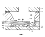
ここで図6を参照すると、例示的な実施形態による、図5A〜Bに関して説明した噴射アセンブリ200の様々な構成要素を示すより詳細な図が示されている。示すように、作動ビーム240は、作動部242、チューニング層244、および不活性層246を備える。不活性層246は、チューニング層244および作動部242のベースとして機能する。作動部242およびチューニング層244の構造は、図7に関してより詳細に記載されている。いくつかの実施形態では、不活性層246は、シリコンまたは他の好適な材料で構成される。いくつかの実施形態では、不活性層246、スペーサー部材280、および封止部材290は全て同一の材料(例えば、シリコンウェーハからモノリシックに形成される)で構成される。例示的実施形態では、不活性層246、スペーサー部材280、および封止部材290は、二重シリコンオンインシュレータ(SOI)ウェーハから形成される。SOIウェーハは、第一の二酸化ケイ素層二酸化ケイ素と第二の二酸化ケイ素層との間に位置する第一のシリコン層と、第二の二酸化ケイ素層と第三の二酸化ケイ素層との間に位置する第二のシリコン層と、第三の二酸化ケイ素層の下に位置するベース層とを備えてもよい。
With reference to FIG. 6, more detailed diagrams showing the various components of the
スペーサー部材280は、二つの周辺層の間に挿入される中間層を備えることが示されている。例示的な実施形態では、中間層および不活性層246は、二重SOIウェーハの二つのシリコン層を備え、周辺層はシリコン酸化物層を含む中間層の両側に配置される。この実施例では、封止部材290およびスペーサー部材280は、作動部242の反対側の二重SOIウェーハの表面をエッチングすることによって形成される。酸化物層は、エッチングプロセスを一度制御または停止する役割をし、例えば、スペーシング部材280を形成する中間層の全体が、スペーシング部材280と封止部材290を分離する領域内で除去される。このようなプロセスは、スペーシング部材280および封止部材290の幅および厚さの両方に対する正確な制御を提供する。
The
理解されるように、封止部材290のサイズは、作動ビーム240の共振周波数に寄与してもよい。作動ビーム240の端部に、またはその近くに配置される材料の量が多いと、一般的に作動ビームの共振周波数が低くなる。さらに、このようなより大きな量の材料は、作動ビーム240に接触する加圧流体から誘導される作動ビーム240の初期湾曲に影響を与えるであろう。したがって、封止部材290の所望のサイズは、作動ビーム240の様々な他の設計の選択に影響を与える。このような設計の選択は、図7Aに関してより詳細に記載されている。いくつかの実施形態では、封止部材290は、オリフィス260の寸法に基づいてサイズ決めされる。いくつかの実施形態では、封止部材290は、実質的に円筒形であり、オリフィス260の直径の約1.5倍の直径を有する。例えば、一実施形態では、封止部材290は、オリフィス260が約60ミクロンの直径を有する場合、約90ミクロンの直径を有する。このような構成は、封止部材290がバルブシート270に接触するとオリフィス260を完全に覆うように、封止部材290とオリフィス260との間の位置合わせを容易にする。別の実施形態では、封止部材290は、オリフィス260の表面積の約2倍の表面積を有するようにサイズ決めされる(例えば、スペーサー部材280は約150ミクロンの直径を有してもよく、オリフィス260は直径約75ミクロンである)。このような実施形態は、封止部材290とオリフィス260との位置合わせに、より大きな許容差を提供し、バルブシート270と封止部材290との間の封止を生成し易くする。別の実施形態では、封止部材290の直径は、オリフィス260の直径の2倍、2.5倍、3倍、3.5倍、または4倍であってもよい。様々な実施形態では、オリフィス260の長さの直径に対する比は、1:1〜15:1の範囲内であってもよい。比率は、オリフィスを通して吐出される流体液滴の形状、サイズ、および/または体積に影響を与えている可能性があり、特定の用途に基づいて変化してもよい。
As will be appreciated, the size of the sealing
有利なことに、スペーシング部材280と封止部材290との間のビア324は、作動ビーム240とオリフィスプレート250との間の分離体積326を生成する。分離体積326は、作動ビーム240の振動のスクイーズフィルムダンピングを防止する。言い換えると、オリフィスプレート250と作動ビーム240との間の不十分な分離は、作動ビーム240がオリフィス260を開閉するにつれて、分離体積326に出入りしなければならない流体から生じる抗力につながる。スペーサー部材280を介して生成されるより大きな分離体積を有することにより、このような抗力は低減され、したがって作動ビーム240はより速い周波数で振動し易い。
Advantageously, the via 324 between the spacing
引き続き図6を参照すると、オリフィスプレート250は、ベース層252および中間層254を備える。例えば、一実施形態では、ベース層252はシリコン層を備え、中間層254はシリコン酸化物層を備える。示す実施形態では、オリフィス260に近接する中間層254の一部分が取り除かれ、バルブシート270の第一の部分がベース層252上に直接配置され、バルブシート270の第二の部分が中間層254上に配置される。別の実施形態では、中間層254はオリフィス260の境界までずっと延在し、バルブシート270は中間層254上に配置されることを理解されたい。さらに別の実施形態では、中間層254の除去される部分は、バルブシート270がベース層252上に完全に配置されるように、バルブシート270の断面と等しいか、またはそれよりも大きい断面を有してもよい。
Continuing with reference to FIG. 6, the
スペーサー部材280とバルブシート270との間の空間的関係の重要度により、スペーサー部材280のオリフィスプレート250への取付けは、作動ビーム240とオリフィスプレート250との間の結果として生じる距離を正確に制御できる方法で実施されてもよい。示すように、接着層256を使用して、スペーサー部材280をオリフィスプレート250に取り付ける。様々な実施形態では、エポキシ系接着剤(例えば、SU−8、ポリメチルメタクリレート、シリコーン等)の正確な量が中間層254に塗布され、その後、その上にスペーサー部材280と作動ビーム240との組み合わせが配置される。次に接着剤を硬化させて、正確に制御された厚さを有する接着層256を形成する。例えば、いくつかの実施形態では、スペーサー部材280の最下層表面は、バルブシート270の上面と実質的に位置合わせされる。作動ビーム240が初期位置にある場合、このような表面間の任意の所望の関係を取得して、封止部材290とバルブシート270との間の適切な封止を生成することができる。様々な実施形態では、接着層256およびバルブシート270は、単一のフォトリソグラフィープロセスにおいて同一の材料(例えば、SU−8)から形成されてもよい。
Due to the importance of the spatial relationship between the
様々な実施形態では、作動ビーム240とオリフィスプレート250が接着剤層256を介して(例えば、マイクロバルブ230を形成するために)互いに取り付けられると、別の接着剤層248が作動ビーム240の周辺部に適用される。別の接着層248を使用して、入力流体マニホールド210を作動ビーム240に取り付ける。構造層222(またはインターポーザ222b)は、入力流体マニホールド210上に配置され、第二の接着層225を介してそれに連結してもよい。いくつかの実施形態では、別の接着層248および第二の接着層225は、接着層256と同じ材料を含んでもよい。
In various embodiments, when the working
図6に関して示す実施例では、マイクロバルブ230は、様々な構成要素を備える封止構造500を備え、それにより封止が形成されてオリフィス260を作動ビーム240に近接する体積から分離する。示す実施例では、封止構造500は、封止部材290およびバルブシート270を備える。本明細書に記載のように、作動ビーム240は、封止部材290のオリフィスに面する表面が、バルブシート270の上面と接触して、バルブシート270と封止部材290との間のインターフェースで封止を形成するように構成される。封止は、オリフィス260をチャネル212から分離し、作動ビーム240に電気信号が印加されない場合、最小限の流体が噴射アセンブリ200から漏れ出るようにする。別の実施形態では、オリフィス260を流体的に封止するために、封止構造500のオリフィスに面する表面がオリフィスプレート250に接触するように、バルブシート270は除外されてもよい。
In the embodiment shown with respect to FIG. 6, the
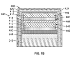
ここで図7Aを参照すると、例示的な実施形態にしたがって作動ビーム240のより詳細な図が示され、図は縮尺通りではない。示すように、作動ビーム240は、不活性層246、チューニング層244およびバリア層400、第一の電極部402、作動部242、第二の電極部404、ならびにパッシベーション構造体406を備えるベース層を備えてもよい。理解されるように、様々な別の実施形態では、作動ビーム240は、より多くの層またはより少ない層を備えてもよい。
Here, with reference to FIG. 7A, a more detailed view of the working
いくつかの実施形態では、チューニング層244は、不活性層246上に直接配置される。チューニング層244は、一般的に本明細書に記載の別の層を堆積し易くするために接着層として機能する。さらに、本明細書に記載のように、チューニング層244の厚さは、その初期位置にある場合に作動ビーム240の全体の湾曲を決定する上で重要な役割を果たす場合がある。一般的に言えば、チューニング層244は、閉位置において、オリフィス260を流体的に封止するために、作動ビーム240の封止部材290がバルブシート270に接触し、力を加えるように、所定の調整応力を有するように構成される。いくつかの実施形態では、バルブシート270がない場合、封止部材290の封止部材表面が、スペーサー部材280の下面の下に所定の距離(例えば、2ミクロン)に配置されるように、電気信号がない場合には、所定の調整応力は、作動ビーム240をオリフィス260に向かって湾曲させるように構成される。例えば、チューニング層244は、本明細書に記載の別の層の堆積の結果として圧縮応力の状態に置かれてもよい。したがって、より厚いチューニング層244は、その初期位置にある場合、オリフィス260に向かって作動ビーム240をより大きく湾曲させる。例示的な一実施形態では、チューニング層244は二酸化ケイ素で構成される。
In some embodiments, the
バリア層400は、第一の電極部402に含まれる材料のチューニング層244への拡散に対するバリアとして機能する。チェックをしないままにしておくと、このようなマイグレーションは、層内の構成材料間の有害な混合効果をもたらし、性能に悪影響を与える。様々な実施形態では、バリア層400は、例えば、二酸化ジルコニウムから構成される。示すように、第一の電極部402は、接着層408および第一の電極410を備える。接着層408は、バリア層400上に第一の電極410を堆積し易くし、第一の電極410内の物質の他の層への拡散を防止する。様々な実施形態では、接着層408は、二酸化チタンから構成される。第一の電極410は、作動部242に送られる電気信号のための導電性経路を提供するために、白金、金、ルビジウム、または任意の他の好適な導電性材料から構成されてもよい。いくつかの実施形態では、第一の電極部402は、作動ビーム240の選択部分にのみ備えられる。例えば、第一の電極部402は、電気接続部294に近接して、および/または電気接続部294内にのみ備えられてもよい。
The
作動部242は、任意の好適な圧電材料の単一または複数の層から形成されてもよい。示す実施例では、活性部分は、成長テンプレート層412および圧電層414を備える。成長テンプレート層412は、最大限の圧電応答を確実にするために、所望のテクスチャー(例えば、{001}テクスチャー結晶構造および対応するテクスチャー)を有する圧電層414の成長を促進するシード層として機能する。いくつかの実施形態では、成長テンプレート層412は、チタン酸鉛で構成される。圧電層414は、任意の好適な材料、例えば、チタン酸ジルコン酸鉛(PZT)で構成されてもよい。
The actuating
圧電層414を、任意の方法を使用して、例えば、真空堆積またはゾル−ゲル堆積技術を利用して堆積してもよい。いくつかの実施形態では、圧電層414は、約1〜6ミクロン(例えば、1、2、3、4、5、または6ミクロンを含む)の範囲の厚さを有してもよく、電気信号がそれに印加される場合、作動ビーム240の端部で約10ミクロンの撓みを生成するように構成される。10ミクロンの撓みは(例えば、封止部材290の表面がバルブシート270からその量よりもわずかに少ない量だけ離れるように)、所望のサイズを有するオリフィス260に液滴を生成するのに十分であってもよい。いくつかの実施形態では、圧電層414は、約140〜160pm/Vの圧電定数(d31値)の大きさを有する。この値は、作動ビーム240の適切な撓みが、第一の電極部402および第二の電極部404に送られる電気信号により生成されることを可能にしてもよい。
The
示すように、第二の電極部404は、作動部242上に配置される。様々な実施形態では、第二の電極部404は、本明細書に記載の第一の電極部402と同様に構成される。したがって第一の電極部402および/または第二の電極部404への電圧の印加は、圧電層414内の歪みを誘導し、片持ち梁部308をオリフィスプレート250から離れる方向に屈曲させる。第一の電極部402および第二の電極部404に周期制御信号を印加することにより、作動ビーム240の周期サイクルは、所望の周波数でオリフィス260から吐出される液滴を生成する。図7Aは、第一の電極部402と第二の電極部404とが互いに重なり合うことを示すが、他の場所では、第一の電極部402と第二の電極部404とが重なり合っていなくてもよい。これは、圧電層414を損傷する、または電気短絡を引き起こす可能性がある、第一の電極部402と第二の電極部404との間の電子漏れを制限または防止することができる。
As shown, the
様々な実施形態では、第一の電極部402および第二の電極部404に含まれる電極は、非アニーリング状態で堆積される。結果として、電極は実質的に圧縮状態で堆積され、これは初期位置にある場合、作動ビーム240の全体的な湾曲に影響を与える。圧電層414の堆積モードは、電極の圧縮状態に影響を与える可能性がある。例えば、圧電層414が(例えば、気相堆積技術により)堆積され、その後、所定の温度(例えば、約700℃)で硬化されるいくつかの状況では、硬化により電極410をアニールし、圧縮状態が除去されてもよい。このような除去は、作動ビーム240における応力の全体的バランスに影響を与え、これがその初期湾曲を変える。したがって、圧電層414のための低温堆積プロセス(例えば、低温ゾルゲル堆積プロセスまたはプラズマ増強化学気相堆積プロセス)を使用して、電極内の応力の反転を防止することが有益であってもよい。様々な実施形態では、第二の電極部404を、例えば、チューニング層244に所定の調整応力を生成するために、第一の電極部402よりも高い温度でアニールしてもよい。
In various embodiments, the electrodes included in the
図7Aに示す材料は、作動ビーム240の長さに実質的に全体にわたって延在してもよい。したがって、電極部402および404と、マイクロバルブ230により形成される貯留部との間に重なり合いがある。様々な実施形態では、貯留部内に収容される流体は、第一の電極部402および第二の電極部404を形成する材料に対して導電性および/または腐食性である。したがって、電極部402および404を貯留部から分離して、貯留部内に収容される流体が電極部402および404と接触するのを防止することが好ましい。
The material shown in FIG. 7A may extend substantially across the length of the working
これに関して、パッシベーション構造体406は、このような分離を行うように構成される。示す実施例では、パッシベーション構造体406は、誘電体層416、絶縁体層418、およびバリア層420を備える。バリア層420は窒化ケイ素で構成されてもよく、電極部402および404の腐食を防止するために、流体中に含まれる水分子およびイオンに対する拡散バリアとして機能する。いくつかの実施形態では、絶縁体層418は、バリア層420内の引張応力とほぼ釣り合う、圧縮応力を有する二酸化ケイ素層を備える。誘電体層416は、作動ビーム240内に含まれる別の層の酸化を防止するために酸化アルミニウムで構成されてもよい。いくつかの実施形態では、別の金属層はバリア層420上に配置される。例えば、金属層は、パッシベーション構造体406の保護特性をさらに強化するために、酸化タリナム(Talinum oxide)または任意の他の好適な耐薬品性金属で構成されてもよい。特定の実施形態では、バリア層420は、テフロン(登録商標)またはパリレンで形成されてもよい。別の実施形態では、作動ビーム240の少なくとも一部分、すなわち、図7Aに示す層により形成される構造体は、テフロン(登録商標)層またはパリレン層によって覆われるか、またはオーバーコートされてもよい。このようなオーバーコートは、マイクロクラックが作動ビーム240の層内に形成されるのを防止することができる。さらに別の実施形態では、オーバーコートは、金属層、例えば、タンタル層またはパラジウム層を備えてもよい。
In this regard, the
パッシベーション構造体406の追加は、作動ビーム240の初期位置決めに著しく影響する場合がある。これは、パッシベーション構造体406が作動ビーム240の圧縮の中立軸422からずれるためである。示すように、中立軸422は、不活性層246内であり、これは、電極部404およびパッシベーション構造体406が、作動ビーム240内でそこから最も遠くにあることを意味する。こうであるとすれば、このような層で誘発される引張応力または圧縮応力は、作動ビーム240の初期湾曲に大きく影響するであろう。したがって、チューニング層244の厚さは、パッシベーション構造体406の様々な構成層の構造体に基づいて選択される。
The addition of the
図7Bは、例示的な実施形態による、および縮尺通りではない、作動ビーム240に備わる層のそれぞれの配置を示す、作動ビーム240の正面断面図である。示すように、作動ビーム240は、図7Aに関して説明したように、不活性層246、チューニング層244、およびバリア層400を備える。第一の電極部402は、バリア層400上に配置される接着層408(例えば、チタン)、およびその上に配置される導電層または電極410(例えば、白金、金、ルビジウム)を備える。第一の電極部402は、作動ビーム240の長手方向軸に垂直方向の電極部402の端部が、同じ方向にバリア層400の端部の内側に位置するように、バリア層400の幅よりも小さい幅を有するように構成される。
FIG. 7B is a front sectional view of the working
シード層412および圧電層414を備える作動部242は、第一の電極部402の横方向の端部を越えて延在してバリア層400に接触するように、第一の電極部402上に共形に配置される。このようにして、圧電層は、第二の電極部404と重なり合う、または近接する第一の電極部402の少なくとも部分を完全に取り囲む、または囲む。第二の電極部404は、接着層403(例えば、チタン)および導電層405(例えば、白金、金、またはルビジウム)を備える。いくつかの実施形態では、第二電極部404は、圧電層414上に直接配置される導電層405のみを備えてもよい(すなわち、接着層403は省略される)。作動部242は、第一の電極部402の端部と重なり合い、またその端部を越えて延在するので、作動ビーム240の性能に有害な可能性のある電子漏れおよび電流マイグレーションを防止するように、作動部は、第一の電極部402を第二の電極部404から効果的に電気的に絶縁する。
The actuating
パッシベーション構造体406は、他の層246、244、400、402、242、および404のそれぞれの露出部分を共形にコーティングする。しかし、不活性層246の底面は、パッシベーション構造体406でコーティングされなくてもよい。パッシベーション構造体406は、誘電体層416、絶縁体層418、バリア層420、およびトップパッシベーション層424を備えてもよい。バリア層420は窒化ケイ素で構成されてもよく、電極部402および404の腐食を防止するために、流体中に含まれる水分子およびイオンに対する拡散バリアとして機能する。しかし、窒化ケイ素は、一般的に、残りの層上に一旦堆積されると、引張応力状態にある。絶縁体層418は、このような引張応力に釣り合うように構成される。例えば、いくつかの実施形態では、絶縁体層418は、バリア層420内の引張応力とほぼ釣り合う圧縮応力を有する二酸化ケイ素層を備える。様々な実施形態では、バリア層420は、絶縁体層418の下に配置される。誘電体層416は、作動ビーム240内に含まれる別の層の酸化を防止するために、酸化アルミニウム、酸化チタン、酸化ジルコニウム、または酸化亜鉛で構成されてもよい。したがって、パッシベーション構造体406は、作動ビーム240において、腐食および酸化−流体の存在によって引き起こされる二つの主要な欠陥源−の両方を防止する働きをし、したがって、マイクロバルブ230の長期性能を確保する。さらに、トップパッシベーション層424は、バリア層420上に配置され、テフロン(登録商標)またはパリレン層を備えてもよい。このようなオーバーコートは、マイクロクラックが作動ビーム240の層内に形成されるのを防止することができ、また下にある層がプラズマ放電するのを防止することができる(例えば、埋込層は、その後の製造作業において露出されてもよい)。特定の実施形態では、トップパッシベーション層424は、金属層、例えば、タンタル層またはパラジウム層を備えてもよい。いくつかの実施形態では、別の金属層はバリア層420上に配置される。例えば、金属層は、パッシベーション構造体406の保護特性をさらに強化するために、酸化タリナム(Talinum oxide)または任意の他の好適な耐薬品性金属で構成されてもよい。
ここで図8Aを参照すると、例示的な実施形態による、図5A〜Bに関して説明した第二のチャネル214または214b内の第一の電気接続部294の断面図が示されている。第一の断面は、上部電極層404(本明細書では「第二の電極層404」とも呼ばれる)の一部が活性である、すなわち、ワイヤボンド220に電気的に結合する上部電極を形成するように、作動ビーム240の作動に関与する、マイクロバルブ230の第一の位置に沿って切り取られている。活性上部電極は、電気接続部294から片持ち梁部308に向かって延在する。示すように、電気接続部294は、スペーサー部材280上に配置される。スペーサー部材280は、図5A〜Bおよび6に関して説明したオリフィスプレート250上に配置されている。示す実施例では、作動ビーム240は、第一の端部および第二の端部を備える。作動ビーム240は、電気接続部294の全体を通して連続的に延在する不活性層246およびチューニング層244を備えるベース層245、およびバリア層400を備える。このような配置は、それが二重SOIウェーハからの作動ビームを形成し易くするので、マイクロバルブ230の構成を単純化する。しかし、別の実施形態が想定される。例えば、いくつかの代替的な実施形態では、ビアは、チューニング層244および/または不活性層246内に形成されてもよい。圧電材料の層414は、ベース層245上に配置され、第一の端部と第二の端部との間の距離の一部を延在する。第一のビア802および第二のビア804は、電気接続部294において、層414および成長テンプレートまたはシード層412に透設される。
Here, with reference to FIG. 8A, a cross-sectional view of the first
図示した実施形態では、作動ビーム240の特定の層は、電気接続部294の特定の領域に含まれない。例えば、示すように、第二の電極層404は、電気接続部294の電極領域800にのみ備えられる。様々な実施形態では、電極領域800は、作動ビーム240の末端部328よりもベース部306に近接して配置される。したがって、末端部328に近接する電気接続部294の領域は、第二の電極層404を含まない。示す実施例では、下部電極層402(以下、「第一の電極層402」と呼ぶ)は、電極領域800の限定されたセグメントにのみ配置される。図8Aに示す第一の位置において、第一のビア802の下に配置される下部電極層402の一部は不活性であり、すなわち、作動ビーム240の作動において何の役割も果たさない。以下でさらに詳細に説明するように、例えば、製造プロセス中に、第一の位置で第一のビア802の下に配置される下部電極層402の部分は、物理的に切断されるように構成されてもよく、それにより、下部電極層402が片持ち梁部308内に延在する下部電極を形成する、マイクロバルブ230の第二の位置に位置する下部電極層402の活性部分から電気的に切断される。したがって、この限定されたセグメント内で、作動ビーム240は、作動ビーム240の他のいずれのセグメントよりも多くの層を備える。結果として、作動ビーム240は、電極領域800内の最大厚さを有してもよい。
In the illustrated embodiment, the particular layer of the working
示すように、電気接続部294内に、圧電層414は、第一のビア802および第二のビア804を備える。示す実施例では、作動ビーム240の別の層はまた、第一のビア802および第二のビア804と同一時空間に広がるビアも備えてもよい。例えば、示すように、成長テンプレート層412はまた、圧電層内の第一のビア802に対応するビアを備える。そのようなビアは、例えば、圧電層414が成長テンプレート層412上に形成された後に形成されてもよい。例えば、エッチングマスクを圧電層414上に配置することができ、層412および414の一部が第一のビア802に対応する位置で除去されるように、エッチャントを圧電層414に塗布してもよい。本明細書に前記のように、下部電極層402の部分は、第一のビア802の下に配置される。上部電極層404の一部は、第一のビア802を介して配置され、下部電極部402の不活性部分の上に配置される。
As shown, within the
第二のビア804は、ベース層245まで圧電材料414の層に透設される。ボンディングパッド806は、ボンディングパッド806の少なくとも一部がベース層245上の第二のビア804を通って配置されるように、作動ビーム240上に配置される。ボンディングパッド806は、ワイヤボンド220を受け入れるように構成される。いくつかの実施形態では、第二のビア804は、ボンディングパッド806がチューニング層244上に堆積されるように、バリア層400に透設されてもよい。チューニング層244は、圧電材料層414およびバリア層400のよりも実質的に剛性がより高くてもよく、ボンディングパッド806がその上にワイヤボンド220を受け入れるように、非常により高い剛性かつより高い堅牢な表面を提供することができる。図8Aに示すように、ボンディングパッド806は、第一のビア802内に配置される主要部808と、圧電層414の上面に配置されるボンディングパッドリード810とを備える。例えば、第一のビア802および第二のビア804が形成された後、ボンディングパッド806は、任意の好適な技術を使用して、圧電層414上および第二のビア804上に堆積されてもよい。様々な実施形態では、ワイヤボンドパッド806は、好適な堆積方法(例えば、スパッタリング、熱蒸発、電子ビーム蒸発、ゾルゲルコーティング等)を使用して金で構成される。主部分808は第二のビア804内のベース層245上に堆積され、一方、ボンディングパッドリード810は圧電材料414の層上に配置される。ボンディングパッドリード810の一部は、それに電気的に接続するように、上部電極部404上に第一のビア802で配置される。
The second via 804 is transparent to the layer of the
第一の電極層402および第二の電極層404の一部が電極領域800内に含まれる(または第一のビア802の境界を越えて延在しない)結果として、第一の電極層402の一部も第二の電極404の一部も、主要部808とは重なり合わない。有利なことに、このような構造は、ワイヤボンドパッド806の堆積およびワイヤボンド220のワイヤボンドパッド806への接続の結果として電極層402、404に加えられるひずみを低減する。図7A〜Bに関して説明したように、電極部402および404に含まれる電極層は、圧縮応力を有する非アニール状態で堆積されてもよい。その上へのワイヤボンドパッド806の主要部808の堆積は、電極層402、404の圧縮状態を変えることができ、作動ビーム240内の応力のバランスを変更し、それによってその初期位置に影響を与えてもよい。第一のビア802は、電極層402、404からの主要部808の分離を容易にし、それによってこの効果を低減し、したがって、作動ビーム240が所望の初期位置を有することを確実にする。
As a result of a portion of the
示す実施例では、作動ビーム240の別の層は、第二のビア804に対応する位置にビアを備える。成長テンプレート層412は、図示の実施形態ではこのようなビアを備える。したがって、(例えば、第一のビア802および第二のビア804に対応する位置の)作動ビーム内のビアは、作動ビーム240の異なる数の構成層を通って延在してもよい。例えば、第二のビア804では、成長テンプレート層412およびバリア層400の両方が、対応するビアを備える。しかし、第一のビア802には、成長テンプレートレイヤーのみがこのような対応するビアを備える。
In the embodiment shown, another layer of
第一の電極層402の一部は、第一のビア802の下に配置される。示すように、第一の電極層402の部分は、第二のビア804に対して実質的に中心にあり、第二のビア804よりもわずかに大きい。したがって、層412および414の一部、およびその上に配置されるすべての層(例えば、第二の電極層404、ワイヤボンドパッド806、およびパッシベーション構造体406など)は、第一の電極層402の円周方向境界で傾斜してもよい。図8Aの第一の断面が切り取られる第一の位置において、第一の電極層402の部分は、片持ち梁部308まで延在せず、したがって、第一の位置で圧電層414にバイアスをかけることに何の役割も果たさない(すなわち、電気的に不活性である)。
A portion of the
第二の電極層404は、第二の電極部404の一部が第一のビア802内に配置されるように、第一のビア802を横切って延在する。言い換えると、第一のビア802では、第一の電極層402と第二の電極層404は、電気接続部294内の別の位置よりも互いに近い。例えば、第一のビア802の外側の位置で、第一の電極層は、圧電層414の第一の(例えば、下)面に配置され、第二の電極層は、圧電層414の第二の(例えば、上)面に配置される。図示の実施形態では、第一のビア802内で、第一電極層402および第二の電極層404は、(図7A〜Bに関して説明した接着層408と同様に)第二の電極層404の接着層のみによって分離されている。前記のように、第一の位置で、上部電極層の部分は活性であり、上部電極を形成する。上部電極の延長部407は、第二の電極層404の一部から片持ち梁部308上に外向きに延在し、主要部808から片持ち梁部308上に配置される圧電層414の一部に電気信号を伝達するように構成される。
The
ワイヤボンディングパッドのボンディングパッドリード810は、圧電層414の上面を越えて、第一のビア802を横切って延在する。示す実施例では、ボンディングパッドリード810は、第一のビア802を横切って第二の電極層404の一部を越えて延在する。ボンディングパッドリード810と第二の電極層404の一部との間の接触領域は、電気接続を形成し、それを通して、電気信号はワイヤボンド220を介して圧電層414に送られてもよい。本明細書に記載のように、第二の電極層404は、電極領域800から作動ビーム240のベース部(例えば、図5A〜Bに関して説明したベース部306等)、および実質的に全ての片持ち梁部(例えば、図5A〜Bに関して説明した片持ち梁部308等)を横切って延在してもよい。したがって、ボンディングパッドリード810での電気接続部を介して提供される電気信号は、電気信号が片持ち梁部の実質的に全体に容易に送達され、したがって、効率的な圧電応答を促進する。
The bonding pad leads 810 of the wire bonding pads extend beyond the upper surface of the
示すように、パッシベーション構造体406は、圧電層414上に配置される。様々な実施形態では、ボンディングパッド806が形成された後(例えば、第一のビア802および第二のビア804の形成後)、パッシベーション構造体は、任意の好適な堆積技術により作動ビーム240上に配置される。示すように、パッシベーション構造体406は、第一のビア802とほぼ対応するように配置されるビアを備える。パッシベーション構造体406内のこのようなビアは、ワイヤボンド220のための場所を提供する。パッシベーション構造体406内のビアは、パッシベーション構造体406が(例えば、エッチングまたは他のいずれの好適な切断技術によって)電気接続部294を完全に覆うように、パッシベーション構造体406が配置された後に形成さることができる。示すように、パッシベーション構造体406は、腐食を防止するために第二の電極層404を完全に覆う。
As shown, the
図8Bは、例示的な実施形態による、第二の電気接続部294bの断面図であり、これはまた、図5A〜Bに関して説明される第二のチャネル214内のマイクロバルブアセンブリ内に備えられてもよい。断面は、(本明細書では「第一の電極層402」とも呼ばれる)下部電極層402の一部が第二のワイヤボンド220bに電気的に結合するマイクロバルブ230の第二の位置に沿って切り取られている。示すように、電気接続部294bは、スペーサー部材280上に配置される。
FIG. 8B is a cross-sectional view of the second
示すように、第二の電気接続部294b内に、圧電層414は、第一のビア802bおよび第二のビア804bを備える。第二のボンディングパッド806bは、作動ビーム240上に配置されている。第二のボンディングパッド806bは、第二の電気接続部294bに配置される第一の電極部402の一部に電気信号(例えば、電流または電圧)を提供するように構成される。示すように、第二のボンディングパッド806bは、第一のビア802b内に配置される主要部808bと、圧電層414の上面上に配置されるボンディングパッドリード810とを備える。さらに拡大すると、第二の位置で、第一のビア802の下に配置される下部電極層402の部分は、下部電極を形成するように活性である。さらに、下部電極層402の活性部分の上の第一のビア802b内に配置される第二の電極層404の部分は、不活性であり、すなわち、作動ビーム240の作動に関与しない。例えば、本明細書で前記のように、製造プロセス中に、第一のビア802b内に配置される上部電極層404の部分は、物理的に切断されるように構成されてもよく、それにより、上部電極層404が片持ち梁部内に延在するマイクロバルブ230の第一の位置に位置する上部電極層404の活性部分から電気的に切断される。ボンディングパッドリード810bの一部は、上部電極層404の不活性部分上に第一のビア802bで配置され、上部電極層404の不活性部分を介して、およびいくつかの実施形態では第一の電極層402の部分と第二の電極層404の部分との間に挿入される第二の接着層を介しても、下部電極層402の活性部分に電気的に接続される。
As shown, within the second
電極層402および404の部分が電極領域800内に含まれる(または第一のビア802の境界を越えて延在しない)結果として、第一の電極層402も第二の電極404も、主要部808bとは重なり合わない。第一の電極層402の一部は、第一のビア802bの下に配置される。示すように、第一の電極層402の部分は、第一のビア802bに対して実質的に中心にあり、第一のビア802bよりもわずかに大きい。したがって、層412および414の一部、およびその上に配置されるすべての層(例えば、第二の電極層404および第二のボンディングパッド806b、ならびにパッシベーション構造体406b)は、第一の電極層402の円周方向境界で傾斜してもよい。第二の電気接続部294bは、以下の違いを除いて、電気接続部294と同様である。図8Bの第二の断面が切り取られる第二の位置で、第二の電極層404は片持ち梁部308まで延在せず、したがって、第二の位置で圧電層414にバイアスをかける役割を果たさない。しかし、第一の電極延長部403bは、第一の電極層402の一部から片持ち梁部308上に外向きに延在し、電気信号を第二の主要部808bから片持ち梁部308上に配置される圧電層414の一部に伝達するように構成される。
As a result of the portions of the electrode layers 402 and 404 being contained within the electrode region 800 (or not extending beyond the boundary of the first via 802), both the
いくつかの実施形態では、マイクロバルブを開閉するために、差動電気信号(例えば、差動電圧)を第一の電極層402の活性部分と第二の電極層404との間に印加してもよい。例えば、本明細書で前述したように、第一の電極層402および第二の電極層404の活性部分に電気信号が印加されていない場合(すなわち、初期位置にある場合)、作動ビーム240は、オリフィスプレート262のオリフィス260を閉じるように構成されてもよい。電気信号の印加に、圧電層414にバイアスをかけ、作動ビーム240に、片持ち梁部308がオリフィス260から離れるように屈曲し、それによってマイクロバルブを開くようにさせてもよい。電気信号は、第一の電極層402または第二の電極層404のいずれか一つ、および電気的接地(例えば、共通接地)に電気的に結合する第一の電極層402および第二の電極層404のいずれか一つに印加されてもよい。
In some embodiments, a differential electrical signal (eg, differential voltage) is applied between the active portion of the
ここで図9を参照すると、例示的な実施形態による、作動ビーム240の片持ち梁部308の端部340の断面図が示されている。示すように、第二の電極部404は、作動ビーム240のほぼ第二の端部338まで延在する。しかし、電極部404の円周方向境界900は、第二の端部338の内側にある。結果として、パッシベーション構造体406が第二の電極部404上に配置されると、パッシベーション構造体406の傾斜部902が第二の端部338に形成される。別の実施形態では、パッシベーション構造体406は、第二の端部338で作動ビーム240の構成層上に共形にコーティングされてもよい。示すように、第二の電極部404の端部340は、傾斜部902により貯留部300から流体的に分離される。第二の電極部404が第二の端部138までずっと延在する場合、円周方向境界900を定める面は貯留部300に露出され、第二の電極部404の腐食が生じるであろう。理解されるように、傾斜部902は、第二の端部338に限定されないが、片持ち梁部308の外周の実質的に全体に延在してもよい。
Here, with reference to FIG. 9, a cross-sectional view of the
傾斜部902は、図9に示されるものとは別の形態をとってもよいことを理解されたい。傾斜部902は実質的に直線的に傾斜しているとして示されているが、当然のことながら別の実施形態では、傾斜部902は湾曲した形態または丸みを帯びた形態を有してもよい。一般的に、傾斜部902は、第二の電極部402の周りを包み込むパッシベーション構造体406の末端部として記載されてもよい。
It should be understood that the
ここで図10を参照すると、例示的な実施形態による、マイクロバルブの作動ビーム1000の平面図が示されている。作動ビーム1000は、本明細書に記載の作動ビーム240と同様の様式で構成されてもよい。示すように、作動ビーム1000は、末端部1002、末端部1002から延在する電気接続部1004、電気接続部1004から延在するベース部1006、およびベース部から延在する片持ち梁部1008を備える。一実施例では、マイクロバルブ内に配置される場合、末端部1002およびベース部1006は、接着剤により入力流体マニホールドに取り付けられる。電気接続部1004は、作動ビームを外部回路基板に接続するためのワイヤボンドのための空間を提供するために、入力流体マニホールドの開口部と位置合わせされてもよい。電気接続部1004は、本明細書に記載の電気接続部294と同様に構成されてもよい。片持ち梁部1008は、入力流体マニホールドとマイクロバルブとによって画成される貯留部内に延在してもよく、電気接続部1004を介して受信される電気信号に応答して移動してもよい。
Here, with reference to FIG. 10, a plan view of the
片持ち梁部1008は、延長部1010および封止部1012を備えることが示されている。延長部1010は、ベース部1006から延在し、実質的に台形形状である。このような台形形状は、流体抵抗の減少に起因して、組み込みマイクロバルブの動作周波数を改善する場合がある。本明細書に記載のように、封止部1012は、実質的に円形であり、バルブシートに封止を形成するためにその上に配置される封止部材を有してもよい。
The
示すように、作動ビーム1000は、圧電材料の層1020および電極1014を備える。電極1014は、圧電材料の層1020上に(例えば、図8A−Bおよび9に記載の第二の電極部404に関して記載したのと同様の方法で)配置される。示すように、電極1014は、片持ち梁部1008上に配置される延長部1022を備える。延長部1022は、作動ビーム1000の円周方向境界1018の内側に配置される円周方向境界1016を有する。このような構造は、作動ビーム1000の境界におけるパッシベーション構造体の末端部を形成し易くし、片持ち梁部1008が接触する可能性がある任意の流体から電極1014の外面を完全に分離する。このような構造は、電極の腐食を低減し、組み込みマイクロバルブの耐久性を向上させる。さらに、電極1014は、可動であるが、作動ビーム1000の不動のベース部1006上に配置される圧電材料1020の第二の部分に連結しない、片持ち梁部1008上に配置される圧電材料1020の第一の部分に通信可能に結合されてもよい。これは、活性化信号(例えば、差動電圧)が電極1014を介して圧電材料1020に送られる場合、圧電材料1020の第二の部分が作動するのを防止してもよい。圧電材料1020の第二の部分は不動であるため、活性化信号の印加は、圧電材料1020を割る可能性がある。したがって、電極1014が圧電材料1020の可動性第一の部分とのみ接触するように設計することは、圧電層の偶発的な故障を防止する。
As shown, the
いくつかの実施形態では、マイクロバルブは、オリフィスを備えるオリフィスプレートと、第一の端部および第二の端部を備える作動ビームと、を備え、作動ビームは、ベース層と、ベース層上に配置され、第一の端部と第二の端部との間の距離の少なくとも一部を延在する圧電材料の層であって、圧電材料の層は、その電気接続部においてそれを通るビアを画成する、圧電材料の層と、圧電材料の層の第一の面上にその電気接続部おいて配置される下部電極層であって、下部電極層の一部はビアの下に配置される、下部電極層と、圧電材料の層の第二の面上にその電気接続部において配置される上部電極層であって、上部電極層の一部はビアを通って配置される、上部電極層と、をさらに備え、作動ビームは、電気接続部から第一の端部に向かって延在するベース部と、ベース部から第二の端部に向かって延在する片持ち梁部と、を備え、片持ち梁部は、下部電極層と上部電極層との間の差動電気信号の印加に応答して、マイクロバルブの開閉のうちの一方に移動可能である。 In some embodiments, the microvalve comprises an orifice plate with an orifice and a working beam with a first end and a second end, the working beam being on the base layer and on the base layer. A layer of piezoelectric material that is arranged and extends at least a portion of the distance between the first and second ends, the layer of piezoelectric material being vias passing through it at its electrical connection. A layer of piezoelectric material and a lower electrode layer that is placed on the first surface of the layer of piezoelectric material at its electrical connection, and a part of the lower electrode layer is placed under the via. A lower electrode layer and an upper electrode layer arranged at its electrical connection on a second surface of a layer of piezoelectric material, a portion of the upper electrode layer being arranged through vias, an upper portion. An electrode layer is further provided, and the working beam has a base portion extending from the electrical connection portion toward the first end portion and a cantilever portion extending from the base portion toward the second end portion. The cantilever portion can move to one of the opening and closing of the microvalve in response to the application of a differential electrical signal between the lower electrode layer and the upper electrode layer.
いくつかの実施形態では、マイクロバルブは、オリフィスプレート上に配置されるバルブシートをさらに備え、バルブシートは、オリフィスおよび流体プレナムと流体連通する開口部を画成する。 In some embodiments, the microvalve further comprises a valve seat disposed on an orifice plate, which defines an opening for fluid communication with the orifice and the fluid plenum.
いくつかの実施形態では、ビアは第一のビアであり、作動ビームの電気接続部において、圧電材料の層はそれを通りベース層まで画成される第二のビアを備え、マイクロバルブはボンディングパッドをさらに備え、ボンディングパッドの少なくとも一部は、ベース層上の第二のビアを通って配置され、ワイヤボンドを受けるように構成される。いくつかの実施形態では、ボンディングパッドは、第一のビアで下部電極層の部分または上部電極層の部分の少なくとも一つに電気的に接続するボンディングパッドリードを備える。 In some embodiments, the via is the first via, at the electrical connection of the working beam, the layer of piezoelectric material comprises a second via that is defined through it to the base layer, and the microvalve is bonded. It further comprises a pad, at least a portion of the bonding pad is arranged through a second via on the base layer and configured to receive a wire bond. In some embodiments, the bonding pad comprises a bonding pad lead that electrically connects to at least one portion of the lower electrode layer or portion of the upper electrode layer with a first via.
いくつかの実施形態では、電気接続部の第一の位置において、下に配置される下部電極層の部分は不活性であり、および、上部電極層の部分は上部電極を形成するように活性であり、上部電極は電気接続部から片持ち梁部に向かって延在し、ボンディングパッドリードの一部は上部電極層の部分上に第一のビアにおいて配置され、それに電気的に接続する。 In some embodiments, in the first position of the electrical connection, the portion of the lower electrode layer placed below is inert, and the portion of the upper electrode layer is active to form the upper electrode. There, the upper electrode extends from the electrical connection towards the cantilever, and a portion of the bonding pad leads is placed on the portion of the upper electrode layer at the first via and electrically connected to it.
いくつかの実施形態では、電気接続部の第二の位置において、上部電極層の部分は不活性であり、および、下部電極層の部分は下部電極を形成するように活性であり、下部電極は電気接続部から片持ち梁部に向かって延在し、ボンディングパッドリードの一部は、第一のビアにおいて上部電極層の不活性部分上に配置され、上部電極層の不活性部分を介して活性下部電極に電気的に接続する。 In some embodiments, in the second position of the electrical connection, the portion of the upper electrode layer is inactive and the portion of the lower electrode layer is active to form the lower electrode, the lower electrode. Extending from the electrical connection towards the cantilever, some of the bonding pad leads are placed on the inert portion of the upper electrode layer in the first via and through the inert portion of the upper electrode layer. Electrically connect to the active lower electrode.
いくつかの実施形態では、マイクロバルブは、オリフィスプレート上に配置されるスペーサー部材をさらに備え、電気接続部およびベース部はスペーサー部材上に配置される。 In some embodiments, the microvalve further comprises a spacer member that is located on the orifice plate, and the electrical connection and base are located on the spacer member.
いくつかの実施形態では、ベース層は、チューニング層およびバリア層を備え、その少なくとも一部は、チューニング層と圧電材料の層との間に挿入され、第二のビアは、ボンディングパッドがチューニング層に接触するように、バリア層を通って延在する。いくつかの実施形態では、ボンディングパッドは金で構成されている。 In some embodiments, the base layer comprises a tuning layer and a barrier layer, at least part of which is inserted between the tuning layer and the layer of piezoelectric material, and the second via is a bonding pad with tuning layer. Extend through the barrier layer to contact the. In some embodiments, the bonding pad is made of gold.
いくつかの実施形態では、電気接続部において、作動ビームは、下部電極の下に配置される第一の接着層と、上部電極の下に配置される第二の接着層とを備え、第一の接着層は下部電極と同一の広がりを持ち、第二の接着層は上部電極と同一の広がりを持つ。いくつかの実施形態では、第一のビア、下部電極層、および上部電極は、第二の接着層のみによって分離される。 In some embodiments, in the electrical connection, the working beam comprises a first adhesive layer located below the lower electrode and a second adhesive layer located below the upper electrode, first. The adhesive layer of No. 1 has the same spread as the lower electrode, and the second adhesive layer has the same spread as the upper electrode. In some embodiments, the first via, the lower electrode layer, and the upper electrode are separated only by a second adhesive layer.
いくつかの実施形態では、作動ビームは、圧電材料の層上に配置されるパッシベーション構造体をさらに備え、パッシベーション構造体は、上部電極および圧電材料の層を完全に覆う。いくつかの実施形態では、パッシベーション構造体は、酸化アルミニウム層と、酸化アルミニウム層上に配置される二酸化ケイ素層と、二酸化ケイ素層上に配置される窒化ケイ素層とを備える。 In some embodiments, the working beam further comprises a passivation structure disposed on a layer of piezoelectric material, which completely covers the top electrode and the layer of piezoelectric material. In some embodiments, the passivation structure comprises an aluminum oxide layer, a silicon dioxide layer disposed on the aluminum oxide layer, and a silicon nitride layer disposed on the silicon dioxide layer.
いくつかの実施形態では、上部電極層は、電気接続部から作動ビームのベース部にわたって連続的に延在し、上部電極層は、片持ち梁部上に配置される延長部を備える。いくつかの実施形態では、パッシベーション構造体が延長部の周縁の外側で圧電材料の層と直接接触するように、上部電極層の延長部の周縁は、圧電材料の層の周縁の内側にある。 In some embodiments, the upper electrode layer extends continuously from the electrical connection to the base of the working beam, and the upper electrode layer comprises an extension that is located on the cantilever. In some embodiments, the periphery of the extension of the upper electrode layer is inside the periphery of the layer of piezoelectric material so that the passivation structure is in direct contact with the layer of piezoelectric material outside the periphery of the extension.
いくつかの実施形態では、下部電極層は、電気接続部から作動ビームのベース部にわたって連続的に延在し、下部電極層は、片持ち梁部上に配置される延長部を備える。いくつかの実施形態では、圧電材料の層は、圧電材料が下部電極層の少なくとも一部を取り囲むように、下部電極層の横方向の端部と重なり合い、それを越えて延在する。 In some embodiments, the lower electrode layer extends continuously from the electrical connection to the base of the working beam, and the lower electrode layer comprises an extension that is located on the cantilever. In some embodiments, the layer of piezoelectric material overlaps and extends beyond the lateral end of the lower electrode layer such that the piezoelectric material surrounds at least a portion of the lower electrode layer.
いくつかの実施形態では、片持ち梁部の重なり合う部分はオリフィスと重なり合い、マイクロバルブは重なり合う部分からオリフィスに向かって延在する封止部材をさらに備え、電気信号がない場合、封止部材はバルブシートに接触してマイクロバルブを閉じる。いくつかの実施形態では、オリフィスおよび封止部材は実質的に円筒形であり、電気信号がない場合に、封止部材がオリフィスを完全に覆うように、封止部材は、オリフィスに対して実質的に中心にあり、オリフィスの直径よりも大きい直径を有する。 In some embodiments, the overlapping portion of the cantilever overlaps the orifice, the microvalve further comprises a sealing member extending from the overlapping portion towards the orifice, and in the absence of an electrical signal, the sealing member is a valve. Contact the seat and close the microvalve. In some embodiments, the orifice and the sealing member are substantially cylindrical and the sealing member is substantially relative to the orifice such that the sealing member completely covers the orifice in the absence of an electrical signal. It is centrally located and has a diameter larger than the diameter of the orifice.
いくつかの実施形態では、片持ち梁部は、ベース部からオリフィスに向かって500〜1,000ミクロンの長さで延在する。いくつかの実施形態では、片持ち梁部は、ベース部から延在する第一の部分と、第一の部分から延在する第二の部分とを備え、第二の部分は、第一の部分とは異なる形状である。いくつかの実施形態では、第一の部分の断面は台形形状であり、第二の部分の断面は円筒形状である。 In some embodiments, the cantilever portion extends from the base portion to the orifice with a length of 500 to 1,000 microns. In some embodiments, the cantilever portion comprises a first portion extending from the base portion and a second portion extending from the first portion, the second portion being the first portion. The shape is different from the part. In some embodiments, the cross section of the first portion is trapezoidal and the cross section of the second portion is cylindrical.
いくつかの実施形態では、マイクロバルブは、オリフィスを備えるオリフィスプレートと、第一の端部および第二の端部を備える作動ビームと、を備え、作動ビームは、ベース層と、ベース層上に配置され、第一の端部と第二の端部との間の距離の少なくとも一部を延在する圧電材料の層であって、圧電材料の層は、その電気接続部においてそれを通りベース層までのビアを画成する、圧電材料の層と、圧電材料の層の第一の面上にその電気接続部において配置される、下部電極層と、圧電材料の層の第二の面上にその電気接続部において配置される、上部電極層と、ボンディングパッドであって、ボンディングパッドの少なくとも一部は、ベース層上のビアを通って配置され、ワイヤボンドを受けるように構成され、ボンディングパッドは下部電極層または上部電極層のうちの少なくとも一つに電気的に接続するボンディングパッドリードを備える、ボンディングパッドと、を備え、作動ビームは、電気接続部から第一の端部に向かって延在するベース部と、ベース部から第二の端部に向かって延在する片持ち梁部と、を備え、片持ち梁部は、下部電極と上部電極との間の差動電気信号の印加に応答して、マイクロバルブの開閉のうちの一方に移動可能である。 In some embodiments, the microvalve comprises an orifice plate with an orifice and a working beam with a first end and a second end, the working beam being on the base layer and on the base layer. A layer of piezoelectric material that is arranged and extends at least a portion of the distance between the first and second ends, the layer of piezoelectric material passing through it at its electrical connection base. On the lower electrode layer and the second surface of the piezoelectric material layer, which is located at its electrical connection on the first surface of the piezoelectric material layer and the piezoelectric material layer, which defines the vias up to the layer. An upper electrode layer and a bonding pad, at least a portion of the bonding pad, which is arranged at its electrical connection, is arranged through vias on the base layer and is configured to receive a wire bond and bond. The pad comprises a bonding pad, which comprises a bonding pad lead that electrically connects to at least one of the lower electrode layer or the upper electrode layer, the working beam directed from the electrical connection towards the first end. It comprises an extending base portion and a cantilever portion extending from the base portion toward the second end, and the cantilever portion is a differential electrical signal between the lower electrode and the upper electrode. In response to the application, it can move to one of the opening and closing of the microvalve.
いくつかの実施形態では、噴射アセンブリは、オリフィスプレートを備えるバルブ本体であって、オリフィスプレートはそれを通って延在する複数のオリフィスを備える、バルブ本体と、複数のマイクロバルブであって、複数のマイクロバルブのそれぞれは、第一の端部および第二の端部を備える作動ビームであって、作動ビームは、さらに、ベース層と、ベース層上に配置され、第一の端部と第二の端部との間の距離の少なくとも一部を延在する圧電材料の層であって、圧電材料の層は、その電気接続部においてそれを通るビアを画成する、圧電材料の層と、圧電材料の層の第一の面上にその電気接続部において配置される下部電極層であって、下部電極層の一部はビアの下に配置される、下部電極層と、圧電材料の層の第二の面上にその電気接続部において配置される上部電極層であって、上部電極層の一部はビアを通って配置される、上部電極層と、を備え、作動ビームは、電気接続部から第一の端部に向かって延在するベース部と、ベース部から第二の端部に向かって延在する片持ち梁部と、を備え、片持ち梁部は、下部電極層と上部電極層との間の差動電気信号の印加に応答して、マイクロバルブの開閉のうちの一方に移動可能である、作動ビームを備える、複数のマイクロバルブと、複数のマイクロバルブのそれぞれに連結し、複数のマイクロバルブのそれぞれの流体貯留部を画成する、流体マニホールドと、を備える。 In some embodiments, the injection assembly is a valve body with an orifice plate, the orifice plate comprising a plurality of orifices extending through it, and a plurality of microvalves. Each of the microvalves of is an actuating beam with a first end and a second end, which are further located in the base layer and on the base layer, the first end and the first. A layer of piezoelectric material that extends at least a portion of the distance between the two ends, and the layer of piezoelectric material is a layer of piezoelectric material that defines vias through it at its electrical connection. The lower electrode layer, which is a lower electrode layer arranged at its electrical connection on the first surface of the layer of the piezoelectric material, and a part of the lower electrode layer is arranged under the via, the lower electrode layer and the piezoelectric material. The working beam comprises an upper electrode layer, which is arranged on the second surface of the layer at its electrical connection, with a portion of the upper electrode layer arranged through vias. A base portion extending from the electrical connection portion toward the first end portion and a cantilever beam portion extending from the base portion toward the second end portion are provided, and the cantilever beam portion is a lower electrode. Multiple microvalves and multiple microvalves with working beams that are movable in one of the opening and closing of the microvalves in response to the application of a differential electrical signal between the layers and the top electrode layer. Each is provided with a fluid manifold, which is connected to each and defines a fluid reservoir for each of the plurality of microvalves.
いくつかの実施形態では、複数のマイクロバルブのそれぞれは、オリフィスプレート上に配置されるバルブシートをさらに備え、バルブシートは、オリフィスおよび流体プレナムと流体連通する開口部を画成する。いくつかの実施形態では、ビアは第一のビアであり、作動ビームの電気接続部において、圧電材料の層はそれを通りベース層まで画成される第二のビアを備え、マイクロバルブはボンディングパッドをさらに備え、ボンディングパッドの少なくとも一部は、ベース層上の第二のビアを通って配置され、ワイヤボンドを受けるように構成される。 In some embodiments, each of the plurality of microvalves further comprises a valve seat disposed on an orifice plate, which defines an opening for fluid communication with the orifice and fluid plenum. In some embodiments, the via is the first via, at the electrical connection of the working beam, the layer of piezoelectric material comprises a second via that is defined through it to the base layer, and the microvalve is bonded. It further comprises a pad, at least a portion of the bonding pad is arranged through a second via on the base layer and configured to receive a wire bond.
いくつかの実施形態では、ボンディングパッドは金で構成されている。いくつかの実施形態では、ボンディングパッドは、第一のビアで下部電極層の部分または上部電極層の部分の少なくとも一つに電気的に接続するボンディングパッドリードを備える。 In some embodiments, the bonding pad is made of gold. In some embodiments, the bonding pad comprises a bonding pad lead that electrically connects to at least one portion of the lower electrode layer or portion of the upper electrode layer with a first via.
いくつかの実施形態では、電気接続部の第一の位置で、下部電極層の部分は不活性であり、および、上部電極層の部分は上部電極を形成するように活性であり、上部電極は電気接続部から片持ち梁部に向かって延在し、ワイヤボンディングリードの一部は第一のビアで上部電極層の部分上に配置され、それに電気的に接続する。 In some embodiments, at the first position of the electrical connection, the portion of the lower electrode layer is inactive and the portion of the upper electrode layer is active to form the upper electrode and the upper electrode is Extending from the electrical connection towards the cantilever, a portion of the wire bonding leads is placed on a portion of the upper electrode layer with a first via and electrically connected to it.
いくつかの実施形態では、電気接続部の第二の位置で、上部電極層の部分は不活性であり、そして、下部電極層の部分は下部電極を形成するように活性であり、下部電極は電気接続部から片持ち梁部に向かって延在し、ワイヤボンディングリードの一部は、上部電極層の不活性部分を通って活性下部電極に電気的に接続するように、第一のビアで上部電極層の不活性部分上に配置される。 In some embodiments, at the second position of the electrical connection, the portion of the upper electrode layer is inactive, and the portion of the lower electrode layer is active to form the lower electrode, the lower electrode. At the first via, extending from the electrical connection towards the cantilever, some of the wire bonding leads are electrically connected to the active lower electrode through the inert portion of the upper electrode layer. It is placed on the inert portion of the upper electrode layer.
いくつかの実施形態では、流体マニホールドの少なくとも一部は、作動ビームの末端部上に配置される。いくつかの実施形態では、流体マニホールドは、複数のマイクロバルブとキャリアとの間に配置され、キャリアは、流体マニホールドおよび複数のマイクロバルブが配置される体積を実質的に囲む。 In some embodiments, at least a portion of the fluid manifold is located on the end of the working beam. In some embodiments, the fluid manifold is located between the plurality of microvalves and the carrier, and the carrier substantially encloses the volume in which the fluid manifold and the plurality of microvalves are located.
いくつかの実施形態では、噴射アセンブリは、流体マニホールドとキャリアとの間に配置されるインターポーザをさらに備える。いくつかの実施形態では、噴射アセンブリは、流体マニホールドとインターポーザとの間に配置されるフレックス回路と、キャリアの側面に取り付けられる回路基板とをさらに備え、フレックス回路は、複数のマイクロバルブの作動ビームを、電気接続部において作動ビームに連結するワイヤボンドを介して回路基板に電気的に接続する。 In some embodiments, the injection assembly further comprises an interposer that is placed between the fluid manifold and the carrier. In some embodiments, the injection assembly further comprises a flex circuit located between the fluid manifold and the interposer, and a circuit board mounted on the side of the carrier, where the flex circuit is a working beam of multiple microvalves. Is electrically connected to the circuit board via a wire bond that connects to the working beam at the electrical connection.
いくつかの実施形態では、マイクロバルブのそれぞれは、オリフィスプレート上に配置されるスペーサー部材をさらに備え、電気接続部およびベース部はスペーサー部材上に配置される。 In some embodiments, each of the microvalves further comprises a spacer member that is located on the orifice plate, and the electrical connection and base are located on the spacer member.
いくつかの実施形態では、電気接続部において、作動ビームは、下部電極層の下に配置される第一の接着層と、上部電極層の下に配置される第二の接着層とを備え、第一の接着層は下部電極層と同一の広がりを持ち、第二の接着層は上部電極層と同一の広がりを持つ。 In some embodiments, in the electrical connection, the working beam comprises a first adhesive layer arranged below the lower electrode layer and a second adhesive layer arranged below the upper electrode layer. The first adhesive layer has the same spread as the lower electrode layer, and the second adhesive layer has the same spread as the upper electrode layer.
いくつかの実施形態では、第一のビアで、下部電極層、および上部電極層は、第二の接着層だけによって分離される。いくつかの実施形態では、作動ビームは、作動ビーム上に配置されるパッシベーション構造体をさらに備え、パッシベーション構造体は、上部電極層を完全に覆う。 In some embodiments, in the first via, the lower electrode layer, and the upper electrode layer, are separated only by the second adhesive layer. In some embodiments, the working beam further comprises a passivation structure disposed on the working beam, which completely covers the upper electrode layer.
いくつかの実施形態では、パッシベーション構造体は、酸化アルミニウム層と、酸化アルミニウム層上に配置される二酸化ケイ素層と、二酸化ケイ素層上に配置される窒化ケイ素層とを備える。いくつかの実施形態では、上部電極層は、電気接続部から作動ビームのベース部にわたって連続的に延在し、上部電極層は、片持ち梁部上に配置される延長部を備える。 In some embodiments, the passivation structure comprises an aluminum oxide layer, a silicon dioxide layer disposed on the aluminum oxide layer, and a silicon nitride layer disposed on the silicon dioxide layer. In some embodiments, the upper electrode layer extends continuously from the electrical connection to the base of the working beam, and the upper electrode layer comprises an extension that is located on the cantilever.
いくつかの実施形態では、パッシベーション構造体が延長部の周縁の外側で圧電材料の層と直接接触するように、上部電極層の延長部の周縁は、パッシベーション構造体の層の周縁の内側にある。 In some embodiments, the rim of the extension of the upper electrode layer is inside the rim of the layer of the passivation structure so that the passivation structure is in direct contact with the layer of piezoelectric material outside the rim of the passivation. ..
いくつかの実施形態では、下部電極層は、電気接続部から作動ビームのベース部にわたって連続的に延在し、下部電極層は、片持ち梁部上に配置される延長部を備える。いくつかの実施形態では、圧電材料の層は、圧電材料の層が下部電極層の少なくとも一部を取り囲むように、下部電極層の横方向の端部と重なり合い、それを越えて延在する。 In some embodiments, the lower electrode layer extends continuously from the electrical connection to the base of the working beam, and the lower electrode layer comprises an extension that is located on the cantilever. In some embodiments, the layer of piezoelectric material overlaps and extends beyond the lateral end of the lower electrode layer such that the layer of piezoelectric material surrounds at least a portion of the lower electrode layer.
本明細書で使用する用語「約」は、概ね所定値の±10%を意味する。例えば、約0.5は0.45および0.55を含み、約10は9〜11を含み、約1000は900〜1100を含む。 The term "about" as used herein generally means ± 10% of a predetermined value. For example, about 0.5 comprises 0.45 and 0.55, about 10 comprises 9-11, and about 1000 comprises 900-1100.
本明細書で使用する用語「連結する」、「接続する」等は、二つの部材が直接的または間接的に互いに結合することを意味する。こうした結合は、固定(例えば、永久的)または可動(例えば、取り外し可能または開放可能)としてもよい。このような結合は、二つの部材、または二つの部材と任意の別の介在部材が互いに単一の単一体として一体的に形成されるか、または二つの部材、もしくは二つの部材と任意の別の介在部材が互いに取り付けられることで達成されてもよい。 As used herein, the terms "connect", "connect", etc. mean that two members are directly or indirectly connected to each other. Such a bond may be fixed (eg, permanent) or movable (eg, removable or openable). Such a bond is such that the two members, or the two members and any other intervening member, are integrally formed as a single unit with each other, or the two members, or any other member and any other. It may be achieved by attaching the intervening members of the above to each other.
本明細書の要素の位置(例えば、「上」、「下」、「上に」、「下に」など)への言及は、単に、図中の様々な要素の方向を説明するために使用される。様々な要素の方向は、別の例示的な実施形態に従って異なってもよく、このような変形は本開示によって包含されることが意図されていることに留意されたい。 References to the location of elements herein (eg, "above", "below", "above", "below", etc.) are used merely to illustrate the orientation of the various elements in the figure. Will be done. It should be noted that the orientation of the various elements may differ according to another exemplary embodiment and such variations are intended to be incorporated by the present disclosure.
例示的な実施形態に示す要素の構成および配置は、例示にすぎない。本開示のいくつかの実施形態のみが詳細に説明されているが、本開示のレビューを行う当業者であれば、列挙された主題の新規の教示および利点から実質的に逸脱することなく、多くの修正(例えば、様々な要素のサイズ、寸法、構造、形状および比率の変形、パラメータの値、取付け配置、材料の用途、色、向き等)が可能であることを容易に理解するであろう。例えば、一体的に形成されたものとして示される要素は、複数の部品または要素から構成されてもよく、要素の位置は逆転されても、または別の方法で変化されてもよく、個別の要素の性質もしくは数または位置は、変更されても、または変化されてもよい。 The configuration and arrangement of the elements shown in the exemplary embodiments is merely exemplary. Although only some embodiments of the present disclosure are described in detail, those skilled in the art reviewing the present disclosure will often be able to do so without substantially deviating from the novel teachings and advantages of the listed subjects. It will be easily understood that modifications of various elements (eg, variations in size, dimensions, structure, shape and proportions of various elements, parameter values, mounting arrangements, material uses, colors, orientations, etc.) are possible. .. For example, an element shown as integrally formed may be composed of multiple parts or elements, the position of the element may be reversed, or it may be changed in another way, and the individual elements. The nature or number or position of is changed or may be changed.
さらに、「例示的」という語は、実施例、例、または図として機能することを意味するために使用される。「例示的」または「実施例」として本明細書に記載の任意の実施形態または設計は、必ずしも他の実施形態または設計よりも好ましいまたは有利であると解釈されるべきではない(および、このような用語は、このような実施形態が必然的に並外れたまたは最上の例であると暗示することを意図するものではない)。むしろ、「例示的」という言の使用は、概念を具体的に示すことを目的としている。したがって、このような全ての修正は、本開示の範囲内に包含されることが意図される。添付の特許請求の範囲から逸脱することなく、他の置換、修正、変更、および省略は、好ましい実施形態および他の例示的な実施形態の設計、動作条件、および配置においてなされてもよい。 In addition, the term "exemplary" is used to mean act as an example, example, or figure. Any embodiment or design described herein as "exemplary" or "example" should not necessarily be construed as preferred or advantageous over other embodiments or designs (and thus). The term is not intended to imply that such an embodiment is necessarily an extraordinary or best example). Rather, the use of the word "exemplary" is intended to demonstrate the concept. Therefore, all such modifications are intended to be included within the scope of this disclosure. Other substitutions, modifications, modifications, and omissions may be made in the design, operating conditions, and arrangement of the preferred and other exemplary embodiments without departing from the appended claims.
本発明の範囲から逸脱することなく、様々な例示的な実施形態の設計、動作条件、および配置において、他の置換、修正、変更、および省略を行うこともできる。例えば、一実施形態で開示される任意の要素は、本明細書で開示される任意の他の実施形態に組み込まれてもよく、または利用されてもよい。また、例えば、任意のプロセスまたは方法の工程の順序またはシークエンスは、別の実施形態に従って変更または再度順序付けされてもよい。任意の手段と機能の条項は、記載された機能を実行するものとして本明細書に記載された構造、ならびに構造的同等物だけでなく同等の構造も包含することを意図している。添付の特許請求の範囲から逸脱することなく、他の置換、修正、変更、および省略は、好ましい実施形態および他の例示的な実施形態の設計、動作構成、および配置において行ってもよい。 Other substitutions, modifications, modifications, and omissions may be made in the design, operating conditions, and arrangement of various exemplary embodiments without departing from the scope of the invention. For example, any element disclosed in one embodiment may be incorporated or utilized in any other embodiment disclosed herein. Also, for example, the process sequence or sequence of any process or method may be modified or reordered according to another embodiment. The provisions of any means and function are intended to include the structures described herein as performing the described functions, as well as structural equivalents as well as equivalent structures. Other substitutions, modifications, modifications, and omissions may be made in the design, operational configuration, and arrangement of preferred and other exemplary embodiments without departing from the appended claims.
Claims (20)
オリフィスを備えるオリフィスプレートと、
第一の端部および第二の端部を備える作動ビームと、を備え、前記作動ビームは、
ベース層と、
前記ベース層上に配置され、前記第一の端部と前記第二の端部との間の距離の少なくとも一部を延在する圧電材料の層であって、前記圧電材料の層は、その電気接続部においてそれを通るビアを画成する、圧電材料の層と、
前記圧電材料の層の第一の面上にその前記電気接続部において配置される下部電極層であって、前記下部電極層の一部は前記ビアの下に配置される、下部電極層と、
前記圧電材料の層の第二の面上にその前記電気接続部において配置される上部電極層であって、前記上部電極層の一部は前記ビアを通って配置される、上部電極層と、をさらに備え、
前記作動ビームは、前記電気接続部から前記第一の端部に向かって延在するベース部と、前記ベース部から前記第二の端部に向かって延在する片持ち梁部と、を備え、前記片持ち梁部は、前記下部電極層と前記上部電極層との間の差動電気信号の印加に応答して、前記マイクロバルブの開閉のうちの一方に移動可能である、マイクロバルブ。 Micro valve
An orifice plate with an orifice and
A working beam comprising a first end and a second end, said working beam.
With the base layer
A layer of piezoelectric material that is disposed on the base layer and extends at least a portion of the distance between the first end and the second end, the layer of piezoelectric material thereof. A layer of piezoelectric material that defines the vias through it at the electrical connection,
A lower electrode layer arranged on the first surface of the layer of the piezoelectric material at the electrical connection portion, and a part of the lower electrode layer is arranged under the via.
An upper electrode layer arranged on the second surface of the layer of the piezoelectric material at the electrical connection portion, and a part of the upper electrode layer is arranged through the via. With more
The working beam includes a base portion extending from the electrical connection portion toward the first end portion and a cantilever portion extending from the base portion toward the second end portion. The cantilever portion is movable in one of the opening and closing of the microvalve in response to the application of a differential electrical signal between the lower electrode layer and the upper electrode layer.
オリフィスを備えるオリフィスプレートと、
第一の端部および第二の端部を備える作動ビームと、を備え、前記作動ビームは、
ベース層と、
前記ベース層上に配置され、前記第一の端部と前記第二の端部との間の距離の少なくとも一部を延在する圧電材料の層であって、前記圧電材料の層は、その電気接続部においてそれを通りベース層までのビアを画成する、圧電材料の層と、
前記圧電材料の層の第一の面上にその前記電気接続部において配置される下部電極層と、
前記圧電材料の層の第二の面上にその前記電気接続部において配置される上部電極層と、
ボンディングパッドであって、前記ボンディングパッドの少なくとも一部は、前記ベース層上の前記ビアを通って配置され、前記ボンディングパッドは前記下部電極層または前記上部電極層のうちの少なくとも一つに電気的に接続するボンディングパッドリードを備える、ボンディングパッドと、をさらに備え、
前記作動ビームは、前記電気接続部から前記第一の端部に向かって延在するベース部と、前記ベース部から前記第二の端部に向かって延在する片持ち梁部と、を備え、前記片持ち梁部は、前記下部電極と前記上部電極との間の差動電気信号の印加に応答して、前記マイクロバルブの開閉のうちの一方に移動可能である、マイクロバルブ。 Micro valve
An orifice plate with an orifice and
A working beam comprising a first end and a second end, said working beam.
With the base layer
A layer of piezoelectric material that is disposed on the base layer and extends at least a portion of the distance between the first end and the second end, the layer of piezoelectric material thereof. A layer of piezoelectric material that defines vias through it to the base layer at the electrical connection,
A lower electrode layer disposed on the first surface of the layer of piezoelectric material at the electrical connection.
An upper electrode layer disposed at the electrical connection on the second surface of the piezoelectric material layer,
A bonding pad, wherein at least a portion of the bonding pad is disposed through the vias on the base layer, and the bonding pad is electrically connected to at least one of the lower electrode layer or the upper electrode layer. With a bonding pad lead to connect to, with a bonding pad,
The working beam includes a base portion extending from the electrical connection portion toward the first end portion and a cantilever portion extending from the base portion toward the second end portion. The cantilever portion is movable in one of the opening and closing of the microvalve in response to the application of a differential electrical signal between the lower electrode and the upper electrode.
オリフィスプレートを備えるバルブ本体であって、前記オリフィスプレートはそれを通って延在する複数のオリフィスを備える、バルブ本体と、
複数のマイクロバルブであって、前記複数のマイクロバルブのそれぞれは、
第一の端部および第二の端部を備える作動ビームであって、前記作動ビームは、
ベース層と、
前記ベース層上に配置され、前記第一の端部と前記第二の端部との間の距離の少なくとも一部を延在する圧電材料の層であって、前記圧電材料の層は、その電気接続部においてそれを通るビアを画成する、圧電材料の層と、
前記圧電材料の層の第一の面上にその前記電気接続部において配置される下部電極層であって、前記下部電極層の一部は前記ビアの下に配置される、下部電極層と、
前記圧電材料の層の第二の面上にその前記電気接続部において配置される上部電極層であって、前記上部電極層の一部は前記ビアを通って配置される、上部電極層と、をさらに備え、
前記作動ビームは、前記電気接続部から前記第一の端部に向かって延在するベース部と、前記ベース部から前記第二の端部に向かって延在する片持ち梁部と、を備え、前記片持ち梁部は、前記下部電極層と前記上部電極層との間の差動電気信号の印加に応答して、前記マイクロバルブの開閉のうちの一方に移動可能である、作動ビームを備える、複数のマイクロバルブと、
前記複数のマイクロバルブのそれぞれに連結し、前記複数のマイクロバルブのそれぞれの流体貯留部を画成する、流体マニホールドと、を備える、噴射アセンブリ。 It ’s a jet assembly,
A valve body comprising an orifice plate, wherein the orifice plate comprises a plurality of orifices extending through the valve body.
A plurality of microvalves, each of the plurality of microvalves
An actuating beam comprising a first end and a second end, said actuating beam.
With the base layer
A layer of piezoelectric material that is disposed on the base layer and extends at least a portion of the distance between the first end and the second end, the layer of piezoelectric material thereof. A layer of piezoelectric material that defines the vias through it at the electrical connection,
A lower electrode layer arranged on the first surface of the layer of the piezoelectric material at the electrical connection portion, and a part of the lower electrode layer is arranged under the via.
An upper electrode layer arranged on the second surface of the layer of the piezoelectric material at the electrical connection portion, and a part of the upper electrode layer is arranged through the via. With more
The working beam includes a base portion extending from the electrical connection portion toward the first end portion and a cantilever portion extending from the base portion toward the second end portion. , The cantilever portion is movable in one of the opening and closing of the microvalve in response to the application of a differential electrical signal between the lower electrode layer and the upper electrode layer. Equipped with multiple micro valves,
An injection assembly comprising a fluid manifold that connects to each of the plurality of microvalves and defines a fluid reservoir for each of the plurality of microvalves.
Applications Claiming Priority (3)
| Application Number | Priority Date | Filing Date | Title |
|---|---|---|---|
| US201862670286P | 2018-05-11 | 2018-05-11 | |
| US62/670,286 | 2018-05-11 | ||
| PCT/IB2019/053838 WO2019215669A1 (en) | 2018-05-11 | 2019-05-09 | Electrode structures for micro-valves for use in jetting assemblies |
Publications (2)
| Publication Number | Publication Date |
|---|---|
| JP2021523332A true JP2021523332A (en) | 2021-09-02 |
| JPWO2019215669A5 JPWO2019215669A5 (en) | 2022-05-16 |
Family
ID=66999875
Family Applications (1)
| Application Number | Title | Priority Date | Filing Date |
|---|---|---|---|
| JP2020563601A Pending JP2021523332A (en) | 2018-05-11 | 2019-05-09 | Electrode structure for microvalves for use in injection assemblies |
Country Status (11)
| Country | Link |
|---|---|
| US (2) | US11186084B2 (en) |
| EP (1) | EP3791098A1 (en) |
| JP (1) | JP2021523332A (en) |
| KR (1) | KR20210018835A (en) |
| CN (1) | CN112352123B (en) |
| AU (1) | AU2019267280A1 (en) |
| BR (1) | BR112020022990A2 (en) |
| CA (1) | CA3099749A1 (en) |
| MX (1) | MX2020012076A (en) |
| TW (1) | TW201947146A (en) |
| WO (1) | WO2019215669A1 (en) |
Families Citing this family (8)
| Publication number | Priority date | Publication date | Assignee | Title |
|---|---|---|---|---|
| BR112020022988A2 (en) | 2018-05-11 | 2021-02-02 | Matthews International Corporation | microvalve and blasting set |
| WO2019215672A1 (en) | 2018-05-11 | 2019-11-14 | Matthews International Corporation | Systems and methods for controlling operation of micro-valves for use in jetting assemblies |
| US11794476B2 (en) | 2018-05-11 | 2023-10-24 | Matthews International Corporation | Micro-valves for use in jetting assemblies |
| BR112020022990A2 (en) | 2018-05-11 | 2021-02-02 | Matthews International Corporation | microvalve and blasting set |
| US11639057B2 (en) | 2018-05-11 | 2023-05-02 | Matthews International Corporation | Methods of fabricating micro-valves and jetting assemblies including such micro-valves |
| AU2020376904A1 (en) * | 2019-11-01 | 2022-06-23 | Matthews International Corporation | Non-contact deposition systems including jetting assemblies |
| KR102256132B1 (en) * | 2020-02-18 | 2021-05-25 | (주)캔탑스 | Automated Material Handling System for Managing Carrier Internal Pollution |
| JP2023004128A (en) * | 2021-06-25 | 2023-01-17 | キヤノン株式会社 | Liquid discharge head |
Family Cites Families (90)
| Publication number | Priority date | Publication date | Assignee | Title |
|---|---|---|---|---|
| DE2527647C3 (en) | 1975-06-20 | 1981-06-25 | Siemens AG, 1000 Berlin und 8000 München | Writing implement that works with liquid droplets |
| US4340083A (en) | 1978-11-30 | 1982-07-20 | Carleton Controls Corporation | Deflectable beam valve |
| DE3114192A1 (en) | 1981-04-08 | 1982-10-28 | Siemens AG, 1000 Berlin und 8000 München | WRITING DEVICE WORKING WITH LIQUID DROPS |
| JPS57197176A (en) | 1981-05-30 | 1982-12-03 | Konishiroku Photo Ind Co Ltd | Ink feeding device in ink jet printer |
| US4450375A (en) | 1982-11-12 | 1984-05-22 | Kiwi Coders Corporation | Piezoelectric fluid control device |
| DE3428969A1 (en) | 1984-08-06 | 1986-02-13 | Siemens AG, 1000 Berlin und 8000 München | CONTROL VALVE FOR AIR VALVE ACTUATION |
| US4564846A (en) | 1984-10-26 | 1986-01-14 | Kiwi Coders Corporation | Drop on demand dot matrix printing head |
| GB8507688D0 (en) * | 1985-03-25 | 1985-05-01 | Lane International Ltd John | Fluid applicator |
| US4629926A (en) | 1985-10-21 | 1986-12-16 | Kiwi Coders Corporation | Mounting for piezoelectric bender of fluid control device |
| EP0243249A1 (en) | 1986-04-18 | 1987-10-28 | Maurice Carre | Dispensing device, particularly for medical use, of a product in a predetermined dosage |
| JPH0694014B2 (en) | 1986-11-07 | 1994-11-24 | マークテック株式会社 | Small high speed spray gun |
| GB8700203D0 (en) | 1987-01-07 | 1987-02-11 | Domino Printing Sciences Plc | Ink jet printing head |
| JPH0773913B2 (en) | 1987-07-14 | 1995-08-09 | マークテック株式会社 | High speed spray gun control method |
| US4962391A (en) | 1988-04-12 | 1990-10-09 | Seiko Epson Corporation | Ink jet printer head |
| JPH0233979A (en) | 1988-07-22 | 1990-02-05 | Matsushita Electron Corp | Optical semiconductor device |
| JP2819141B2 (en) | 1989-02-13 | 1998-10-30 | 株式会社エー・アンド・デイ | Constant speed exhaust device and control method of constant speed exhaust device |
| JPH02273242A (en) | 1989-04-14 | 1990-11-07 | Seiko Epson Corp | Ink jet head |
| DE3935474A1 (en) | 1989-06-22 | 1991-01-03 | Hoechst Ceram Tec Ag | PIEZOELECTRIC BENDING CONVERTER AND ITS USE |
| US5072959A (en) | 1990-11-09 | 1991-12-17 | Marullo Gaetano C | Boat carrier |
| US5126755A (en) | 1991-03-26 | 1992-06-30 | Videojet Systems International, Inc. | Print head assembly for ink jet printer |
| DE4119955C2 (en) | 1991-06-18 | 2000-05-31 | Danfoss As | Miniature actuator |
| JPH05116284A (en) | 1991-10-25 | 1993-05-14 | Canon Inc | Ink jet recording head and ink jet recording apparatus having same |
| GB9302170D0 (en) | 1993-02-04 | 1993-03-24 | Domino Printing Sciences Plc | Ink jet printer |
| US5619177A (en) | 1995-01-27 | 1997-04-08 | Mjb Company | Shape memory alloy microactuator having an electrostatic force and heating means |
| JPH0911471A (en) | 1995-04-26 | 1997-01-14 | Canon Inc | Liquid discharge method, liquid discharge head, head cartridge, liquid discharge device and liquid discharge head kit |
| GB9610819D0 (en) | 1996-05-22 | 1996-07-31 | Lucas Ind Plc | Valve arrangement |
| DE19626428A1 (en) | 1996-07-01 | 1998-01-15 | Heinzl Joachim | Droplet cloud generator |
| DE19648730C2 (en) | 1996-11-25 | 1998-11-19 | Fraunhofer Ges Forschung | Piezo-electrically operated micro valve |
| US6024340A (en) | 1996-12-04 | 2000-02-15 | Active Control Experts, Inc. | Valve assembly |
| US6557977B1 (en) | 1997-07-15 | 2003-05-06 | Silverbrook Research Pty Ltd | Shape memory alloy ink jet printing mechanism |
| JPH11105274A (en) | 1997-10-03 | 1999-04-20 | Marktec Corp | Marking apparatus |
| US5901939A (en) | 1997-10-09 | 1999-05-11 | Honeywell Inc. | Buckled actuator with enhanced restoring force |
| EP1027723B1 (en) | 1997-10-14 | 2009-06-17 | Patterning Technologies Limited | Method of forming an electric capacitor |
| DE29819856U1 (en) | 1998-11-06 | 1999-01-14 | Festo Ag & Co | Control element of a piezo valve |
| DE19857247C1 (en) * | 1998-12-11 | 2000-01-27 | Bosch Gmbh Robert | Piezoelectric actuator for actuating control or injection valves in motor vehicle internal combustion engines |
| GB9828476D0 (en) | 1998-12-24 | 1999-02-17 | Xaar Technology Ltd | Apparatus for depositing droplets of fluid |
| US6358021B1 (en) | 1998-12-29 | 2002-03-19 | Honeywell International Inc. | Electrostatic actuators for active surfaces |
| DE19911399C2 (en) | 1999-03-15 | 2001-03-01 | Joachim Heinzl | Method for controlling a piezo print head and piezo print head controlled according to this method |
| US6164621A (en) | 1999-07-09 | 2000-12-26 | Deka Products Limited Partnership | Simplified piezoelectric valve |
| DE19957959C1 (en) | 1999-12-02 | 2001-01-18 | Festo Ag & Co | Piezovalve manufacturing method has cooperating surfaces between fixing body for piezo flexure element and valve housing used for relative positioning to obtain required closure force |
| EP1106882A3 (en) | 1999-12-09 | 2002-11-13 | Drei-S-Werk Präzisionswerkzeuge GmbH & Co. Fertigungs-KG | Piezo electrically actuated fluid valve |
| US6676249B2 (en) | 1999-12-17 | 2004-01-13 | Eastman Kodak Company | Continuous color ink jet print head apparatus and method |
| JP4288399B2 (en) * | 2000-03-31 | 2009-07-01 | 富士フイルム株式会社 | Multi-nozzle inkjet head and method for manufacturing the same |
| KR100406939B1 (en) | 2000-07-25 | 2003-11-21 | 삼성전자주식회사 | Ink-jet Printer Head |
| DE10048376C2 (en) | 2000-09-29 | 2002-09-19 | Fraunhofer Ges Forschung | Micro valve with a normally closed state |
| US6352337B1 (en) | 2000-11-08 | 2002-03-05 | Eastman Kodak Company | Assisted drop-on-demand inkjet printer using deformable micro-acuator |
| DK1207329T3 (en) | 2000-11-20 | 2003-04-22 | Festo Ag & Co | piezo valve |
| DE10133939C2 (en) | 2001-07-12 | 2003-11-06 | Tally Computerdrucker Gmbh | Method for producing a droplet generator for microdroplets, in particular a nozzle head for ink printers and droplet generators |
| US6464341B1 (en) | 2002-02-08 | 2002-10-15 | Eastman Kodak Company | Dual action thermal actuator and method of operating thereof |
| DK1367307T3 (en) | 2002-05-31 | 2004-08-30 | Festo Ag & Co | piezo valve |
| US7083270B2 (en) | 2002-06-20 | 2006-08-01 | Matsushita Electric Industrial Co., Ltd. | Piezoelectric element, ink jet head, angular velocity sensor, method for manufacturing the same, and ink jet recording apparatus |
| AT412366B (en) | 2002-10-15 | 2005-01-25 | Hygrama Ag | VALVE |
| US7159841B2 (en) | 2002-11-07 | 2007-01-09 | The United States Of America As Represented By The United States Department Of Energy | Piezoelectric axial flow microvalve |
| JP2004308554A (en) | 2003-04-07 | 2004-11-04 | Alps Electric Co Ltd | Fluid pump |
| DE10323773A1 (en) | 2003-05-22 | 2004-12-09 | Heinrich J. Kesseböhmer KG | telescopic extension |
| US6988706B2 (en) | 2003-12-17 | 2006-01-24 | General Electric Company | Piezoelectric microvalve |
| DE102004008009A1 (en) | 2003-12-23 | 2005-07-28 | Robert Bosch Gmbh | Integrated microvalve and method of making a microvalve |
| EP1564464B1 (en) | 2004-02-11 | 2006-04-19 | FESTO AG & Co | Piezo valve |
| WO2006012510A1 (en) | 2004-07-23 | 2006-02-02 | Afa Controls, Llc | Microvalve assemblies and related methods |
| DE102004035844B3 (en) | 2004-07-23 | 2005-10-20 | Siemens Ag | Servo valve for a bridge switch comprises a single common piezoelectric bending element assigned to flow resistors to deviate to two sides in the direction of the counter surfaces |
| KR20060039111A (en) | 2004-11-02 | 2006-05-08 | 삼성전자주식회사 | Inkjet prihthead having cantilever actuator |
| JP4022674B2 (en) * | 2005-03-17 | 2007-12-19 | 富士フイルム株式会社 | Liquid discharge head, image forming apparatus, and method of manufacturing liquid discharge head |
| US20060255064A1 (en) | 2005-05-10 | 2006-11-16 | Par Technologies, Llc | Fluid container with integrated valve |
| CN201022022Y (en) | 2006-11-09 | 2008-02-13 | 大连交通大学 | A conversion device for electrical signals to gas signals |
| DE102007033529A1 (en) | 2007-07-19 | 2009-01-22 | Hoerbiger Automatisierungstechnik Holding Gmbh | Piezoelectric valve |
| DE102007034049B3 (en) | 2007-07-19 | 2008-06-12 | Hoerbiger Automatisierungstechnik Holding Gmbh | Piezoelectric valve has stop provided outside annular face formed by abutting first and second sealing structures and in closed position of flexible element limits deformation of second sealing structure in region of sealing face |
| JP2009243911A (en) | 2008-03-28 | 2009-10-22 | Toray Ind Inc | Defect inspection system |
| CN102202797A (en) | 2008-10-31 | 2011-09-28 | 富士胶卷迪马蒂克斯股份有限公司 | Shaping a nozzle outlet |
| CN102458863B (en) | 2009-06-09 | 2014-07-02 | 录象射流技术公司 | Stream printing method |
| US8556373B2 (en) | 2009-06-19 | 2013-10-15 | Burkhard Buestgens | Multichannel-printhead or dosing head |
| US20110073188A1 (en) | 2009-09-30 | 2011-03-31 | Marcus Michael A | Microvalve for control of compressed fluids |
| US20110073788A1 (en) | 2009-09-30 | 2011-03-31 | Marcus Michael A | Microvalve for control of compressed fluids |
| EP2589140B1 (en) | 2010-06-29 | 2018-08-01 | Hewlett-Packard Development Company, L.P. | Piezoelectric actuator with coplanar electrodes |
| US8529021B2 (en) | 2011-04-19 | 2013-09-10 | Eastman Kodak Company | Continuous liquid ejection using compliant membrane transducer |
| US20140333703A1 (en) | 2013-05-10 | 2014-11-13 | Matthews Resources, Inc. | Cantilevered Micro-Valve and Inkjet Printer Using Said Valve |
| ES2561727B1 (en) | 2014-08-29 | 2017-03-24 | Kerajet S.A. | Device, method and fluid deposition machine on a surface |
| US10434507B2 (en) | 2014-10-22 | 2019-10-08 | The Regents Of The University Of California | High definition microdroplet printer |
| US9763628B2 (en) | 2014-12-31 | 2017-09-19 | Immersion Corporation | Systems and methods for providing enhanced haptic feedback |
| US9975347B2 (en) | 2016-01-08 | 2018-05-22 | Canon Kabushiki Kaisha | Liquid ejection apparatus and liquid ejection method |
| JP2017174985A (en) | 2016-03-24 | 2017-09-28 | キヤノン株式会社 | Processing method for silicon substrate |
| JP2018083385A (en) | 2016-11-25 | 2018-05-31 | キヤノン株式会社 | Film formation method |
| JP2018094845A (en) | 2016-12-15 | 2018-06-21 | キヤノン株式会社 | Liquid discharge head |
| JP6873836B2 (en) | 2017-06-19 | 2021-05-19 | キヤノン株式会社 | Manufacturing method of liquid discharge head |
| JP2019005988A (en) | 2017-06-23 | 2019-01-17 | キヤノン株式会社 | Liquid discharge head and liquid discharge device |
| US11448958B2 (en) | 2017-09-21 | 2022-09-20 | Canon Kabushiki Kaisha | System and method for controlling the placement of fluid resist droplets |
| BR112020022988A2 (en) | 2018-05-11 | 2021-02-02 | Matthews International Corporation | microvalve and blasting set |
| BR112020022990A2 (en) | 2018-05-11 | 2021-02-02 | Matthews International Corporation | microvalve and blasting set |
| US11639057B2 (en) | 2018-05-11 | 2023-05-02 | Matthews International Corporation | Methods of fabricating micro-valves and jetting assemblies including such micro-valves |
| US11794476B2 (en) | 2018-05-11 | 2023-10-24 | Matthews International Corporation | Micro-valves for use in jetting assemblies |
| WO2019215672A1 (en) | 2018-05-11 | 2019-11-14 | Matthews International Corporation | Systems and methods for controlling operation of micro-valves for use in jetting assemblies |
-
2019
- 2019-05-09 BR BR112020022990-3A patent/BR112020022990A2/en not_active Application Discontinuation
- 2019-05-09 WO PCT/IB2019/053838 patent/WO2019215669A1/en active Application Filing
- 2019-05-09 US US16/407,461 patent/US11186084B2/en active Active
- 2019-05-09 CA CA3099749A patent/CA3099749A1/en active Pending
- 2019-05-09 CN CN201980041890.1A patent/CN112352123B/en active Active
- 2019-05-09 MX MX2020012076A patent/MX2020012076A/en unknown
- 2019-05-09 AU AU2019267280A patent/AU2019267280A1/en active Pending
- 2019-05-09 KR KR1020207035810A patent/KR20210018835A/en not_active Application Discontinuation
- 2019-05-09 JP JP2020563601A patent/JP2021523332A/en active Pending
- 2019-05-09 EP EP19732458.5A patent/EP3791098A1/en not_active Withdrawn
- 2019-05-10 TW TW108116314A patent/TW201947146A/en unknown
-
2021
- 2021-11-29 US US17/536,353 patent/US20220219455A1/en not_active Abandoned
Also Published As
| Publication number | Publication date |
|---|---|
| US20190346067A1 (en) | 2019-11-14 |
| TW201947146A (en) | 2019-12-16 |
| BR112020022990A2 (en) | 2021-02-02 |
| AU2019267280A1 (en) | 2020-11-26 |
| US11186084B2 (en) | 2021-11-30 |
| CA3099749A1 (en) | 2019-11-14 |
| EP3791098A1 (en) | 2021-03-17 |
| WO2019215669A1 (en) | 2019-11-14 |
| KR20210018835A (en) | 2021-02-18 |
| CN112352123A (en) | 2021-02-09 |
| US20220219455A1 (en) | 2022-07-14 |
| MX2020012076A (en) | 2021-03-25 |
| CN112352123B (en) | 2023-05-12 |
Similar Documents
| Publication | Publication Date | Title |
|---|---|---|
| JP2021523332A (en) | Electrode structure for microvalves for use in injection assemblies | |
| US11639057B2 (en) | Methods of fabricating micro-valves and jetting assemblies including such micro-valves | |
| US11794476B2 (en) | Micro-valves for use in jetting assemblies | |
| JP2021523039A (en) | Sealed microvalve systems and methods used in injection assemblies | |
| US11660861B2 (en) | Systems and methods for controlling operation of micro-valves for use in jetting assemblies | |
| US20210129173A1 (en) | Non-contact deposition systems including jetting assemblies | |
| JP2024056759A (en) | Systems and methods for sealed microvalves for use in jetting assemblies - Patents.com |
Legal Events
| Date | Code | Title | Description |
|---|---|---|---|
| A521 | Request for written amendment filed |
Free format text: JAPANESE INTERMEDIATE CODE: A523 Effective date: 20220503 |
|
| A621 | Written request for application examination |
Free format text: JAPANESE INTERMEDIATE CODE: A621 Effective date: 20220503 |
|
| A977 | Report on retrieval |
Free format text: JAPANESE INTERMEDIATE CODE: A971007 Effective date: 20230630 |
|
| A131 | Notification of reasons for refusal |
Free format text: JAPANESE INTERMEDIATE CODE: A131 Effective date: 20230704 |
|
| A601 | Written request for extension of time |
Free format text: JAPANESE INTERMEDIATE CODE: A601 Effective date: 20231004 |
|
| A601 | Written request for extension of time |
Free format text: JAPANESE INTERMEDIATE CODE: A601 Effective date: 20231202 |
|
| A02 | Decision of refusal |
Free format text: JAPANESE INTERMEDIATE CODE: A02 Effective date: 20240227 |