JP2021106375A - Image pick-up device and method for controlling the same, and imaging apparatus - Google Patents
Image pick-up device and method for controlling the same, and imaging apparatus Download PDFInfo
- Publication number
- JP2021106375A JP2021106375A JP2020046146A JP2020046146A JP2021106375A JP 2021106375 A JP2021106375 A JP 2021106375A JP 2020046146 A JP2020046146 A JP 2020046146A JP 2020046146 A JP2020046146 A JP 2020046146A JP 2021106375 A JP2021106375 A JP 2021106375A
- Authority
- JP
- Japan
- Prior art keywords
- gain
- signal
- pixel
- image
- read
- Prior art date
- Legal status (The legal status is an assumption and is not a legal conclusion. Google has not performed a legal analysis and makes no representation as to the accuracy of the status listed.)
- Pending
Links
- 238000000034 method Methods 0.000 title claims description 35
- 238000003384 imaging method Methods 0.000 title abstract description 4
- 238000012545 processing Methods 0.000 claims abstract description 33
- 230000003321 amplification Effects 0.000 claims abstract description 32
- 238000003199 nucleic acid amplification method Methods 0.000 claims abstract description 32
- 238000006243 chemical reaction Methods 0.000 claims abstract description 19
- 230000002194 synthesizing effect Effects 0.000 claims description 7
- 230000015572 biosynthetic process Effects 0.000 claims description 2
- 238000003786 synthesis reaction Methods 0.000 claims description 2
- 238000009792 diffusion process Methods 0.000 abstract description 3
- 239000007787 solid Substances 0.000 abstract description 2
- 239000011159 matrix material Substances 0.000 abstract 1
- 238000005070 sampling Methods 0.000 description 15
- 230000002596 correlated effect Effects 0.000 description 14
- 239000000203 mixture Substances 0.000 description 12
- 238000010586 diagram Methods 0.000 description 7
- 230000003287 optical effect Effects 0.000 description 7
- 238000012546 transfer Methods 0.000 description 5
- 238000012937 correction Methods 0.000 description 4
- 239000002131 composite material Substances 0.000 description 3
- 230000001276 controlling effect Effects 0.000 description 3
- 230000006870 function Effects 0.000 description 3
- 238000007599 discharging Methods 0.000 description 2
- 230000002093 peripheral effect Effects 0.000 description 2
- 230000000295 complement effect Effects 0.000 description 1
- 230000000875 corresponding effect Effects 0.000 description 1
- 230000002542 deteriorative effect Effects 0.000 description 1
- 230000000694 effects Effects 0.000 description 1
- 238000011156 evaluation Methods 0.000 description 1
- 210000003127 knee Anatomy 0.000 description 1
- 229910044991 metal oxide Inorganic materials 0.000 description 1
- 150000004706 metal oxides Chemical class 0.000 description 1
- 238000002156 mixing Methods 0.000 description 1
- NJPPVKZQTLUDBO-UHFFFAOYSA-N novaluron Chemical compound C1=C(Cl)C(OC(F)(F)C(OC(F)(F)F)F)=CC=C1NC(=O)NC(=O)C1=C(F)C=CC=C1F NJPPVKZQTLUDBO-UHFFFAOYSA-N 0.000 description 1
- 238000011946 reduction process Methods 0.000 description 1
- 230000011514 reflex Effects 0.000 description 1
- 229920006395 saturated elastomer Polymers 0.000 description 1
- 239000004065 semiconductor Substances 0.000 description 1
- 230000011664 signaling Effects 0.000 description 1
- 230000001629 suppression Effects 0.000 description 1
Images


Abstract
Description
本発明は、画素信号を複数のゲインで増幅して読出すことが可能な撮像素子の動作制御および信号処理の技術に関する。 The present invention relates to an operation control and signal processing technique for an image sensor capable of amplifying and reading a pixel signal with a plurality of gains.
固体撮像素子を備える撮像装置には、2次元配列された画素部で光電変換された映像信号を出力する際、ダイナミックレンジ(以下、DRとも記す)の拡大処理の機能を有するものがある。特許文献1に開示の装置は、単位画素の出力信号に対して列回路内にある増幅部のゲインを切り替え、出力信号がクリップしないようなゲインを決定し、映像信号のDRを向上させることが可能である。特許文献1の図13には、アンプの入力容量を2つ持ち、ゲイン設定部にて入力信号レベルを判定し、その判定結果に応じたゲインに変更することで、2種類のゲインを得る回路が開示されている。この場合、ノイズ信号がどちらか一方のゲインにしか対応しない駆動方法となる。
Some image pickup devices including a solid-state image sensor have a function of expanding a dynamic range (hereinafter, also referred to as DR) when outputting a video signal photoelectrically converted by pixel units arranged in two dimensions. The apparatus disclosed in
また、特許文献2に開示の撮像装置は、入射光量に応じて異なるアンプゲインで増幅された複数の画像信号を用いることでDR拡大が可能である。アンプゲインが異なる2枚の画像について、アンプゲインが大きい方の画像を被写体の低輝度部の画像に用い、アンプゲインが小さい方の画像を被写体の高輝度部の画像に用いて合成処理が実行される。異なるアンプゲインでノイズ成分を読出すには、アンプゲインに対して画素部のリセット回数を十分に確保する必要がある。 Further, the image pickup apparatus disclosed in Patent Document 2 can expand DR by using a plurality of image signals amplified with different amplifier gains according to the amount of incident light. For two images with different amplifier gains, the image with the larger amplifier gain is used as the image in the low-brightness part of the subject, and the image with the smaller amplifier gain is used as the image in the high-brightness part of the subject. Will be done. In order to read out the noise component with different amplifier gains, it is necessary to secure a sufficient number of resets of the pixel portion with respect to the amplifier gain.
ところで、撮像素子では相関二重サンプリングによる信号読出し方法がよく用いられる。この方法では単位画素から、まずノイズ成分を読出し、その後にノイズ成分を含んだ画素信号を読出し、撮像素子内で画素信号からノイズ成分を除去する処理が行われる。特に、内部の増幅回路のゲインが大きいときには、相関二重サンプリングによるノイズ抑制効果が大きい。 By the way, in the image pickup device, a signal reading method by correlated double sampling is often used. In this method, a noise component is first read from a unit pixel, then a pixel signal containing the noise component is read, and a process of removing the noise component from the pixel signal is performed in the image sensor. In particular, when the gain of the internal amplifier circuit is large, the noise suppression effect by the correlated double sampling is large.
同一の画素信号に対して複数のゲインで出力可能な撮像素子では、複数の画像の合成を行う際、特に低輝度部に使用する画像が相関二重サンプリングの行われた画像でないと、ランダムノイズが目立つ画像になる可能性が高くなる。 In an image sensor that can output multiple gains for the same pixel signal, random noise is generated when combining multiple images, especially if the image used for the low-brightness area is not an image that has undergone correlated double sampling. Is more likely to be a prominent image.
本発明の目的は、画素部からの信号ごとに複数のゲインで増幅を行う増幅手段を備え、ノイズ成分をより低減可能な撮像素子を提供することである。 An object of the present invention is to provide an image pickup device that includes an amplification means that amplifies each signal from a pixel unit with a plurality of gains and can further reduce noise components.
本発明の実施形態の撮像素子は、画素部が有する光電変換部からの信号ごとに複数のゲインで増幅を行う増幅手段と、前記増幅手段のゲインを制御する制御手段と、前記増幅手段により増幅された画素信号からノイズ信号を減算する信号処理手段と、を備え、前記制御手段は、前記画素部をリセットした後、前記増幅手段による第1のゲインでノイズ信号と画素信号を読出した後に、前記増幅手段による第2のゲインで画素信号を読出す制御を行い、前記第1のゲインは前記第2のゲインよりも大きいことを特徴とする。 The image pickup device of the embodiment of the present invention is amplified by an amplification means that amplifies each signal from the photoelectric conversion unit of the pixel unit with a plurality of gains, a control means that controls the gain of the amplification means, and the amplification means. The control means includes a signal processing means for subtracting a noise signal from the pixel signal, and the control means reads the noise signal and the pixel signal with the first gain by the amplification means after resetting the pixel portion. A control for reading out a pixel signal with a second gain by the amplification means is performed, and the first gain is larger than the second gain.
本発明の撮像素子によれば、画素部からの信号ごとに複数のゲインで増幅を行う増幅手段を備え、ノイズ成分をより低減可能な撮像素子を提供することができる。 According to the image pickup device of the present invention, it is possible to provide an image pickup device capable of further reducing noise components by providing an amplification means for amplifying each signal from the pixel portion with a plurality of gains.
以下、本発明の各実施形態について図面を参照しながら説明する。本発明はデジタル一眼レフカメラやデジタルスチルカメラ、デジタルビデオカメラ等の撮像素子に適用可能である。撮像素子を構成する画素部から画素信号のみが出力される場合、画素信号の黒レベル(すなわちノイズと近似されるレベル)が判明しないと、映像信号のペデスタルレベルを決定することができない。そのため、画素部や回路部で離散的に発生するランダムノイズの低減が困難となる。例えば、画像合成等の信号処理において、低輝度部に使用される画像に対する相関二重サンプリングが行われた信号でない場合にはランダムノイズの目立つ画像となる可能性がある。以下の実施形態では、ノイズをより低減するとともに黒レベルを決定することができ、画像信号のDR拡大に好適な撮像素子および撮像装置を説明する。 Hereinafter, each embodiment of the present invention will be described with reference to the drawings. The present invention can be applied to an image sensor such as a digital single-lens reflex camera, a digital still camera, or a digital video camera. When only the pixel signal is output from the pixel portion constituting the image sensor, the pedestal level of the video signal cannot be determined unless the black level of the pixel signal (that is, the level approximated by noise) is known. Therefore, it is difficult to reduce the random noise that is discretely generated in the pixel portion and the circuit portion. For example, in signal processing such as image composition, if the signal is not subjected to correlated double sampling for the image used in the low-luminance portion, the image may have conspicuous random noise. In the following embodiments, an image pickup device and an image pickup device that can further reduce noise and determine the black level and are suitable for DR enlargement of an image signal will be described.
[第1実施形態]
図1は、本発明の実施形態に係る撮像装置100の一般的な構成を示すブロック図である。光学レンズ部101は、被写体からの光を取り込んで撮像素子102の受光面上に結像させる。光学レンズ部101は撮像装置100の本体部に装着可能な交換レンズユニット、または本体部に組み込まれたレンズ部であり、撮像光学系を構成するレンズ、絞り等の光学部材を有する。
[First Embodiment]
FIG. 1 is a block diagram showing a general configuration of an image pickup apparatus 100 according to an embodiment of the present invention. The
撮像素子102は光学レンズ部101から入射光を受光し、光電変換によって電気信号を出力する。代表例として、CCD(電荷結合素子)型イメージセンサや、CMOS(相補型金属酸化膜半導体)型イメージセンサ等が挙げられる。撮像素子102には、アナログ映像信号を出力する第1のタイプと、撮像素子102の内部でAD(アナログ・デジタル)変換処理を行ってデジタル映像信号を出力する第2のタイプがある。第2のタイプには、LVDS(Low voltage differential signaling)等によりデジタルデータを出力する形態がある。撮像素子102の構成については図2を用いて後述する。
The
画像取得部103は、撮像素子102から出力された映像信号のキャプチャを行い、各種処理を行う回路部を備える。画像取得部103は、撮像素子102における固定パターンノイズの除去や、黒レベルクランプ処理等を行う。画像取得部103はまた、映像信号の記録に使用する画像信号と、撮像素子102の制御のための評価用信号とに分離する処理を行う。画像取得部103には処理に必要となる設定値を記憶するための内部記憶回路が含まれる。
The
画像合成部104は画像取得部103の出力を取得し、撮像素子102の出力に基づく信号から、任意の合成方法を用いてHDR(高ダイナミックレンジ)画像を生成する。例えば、所定の画像部分(通常画)については高ゲインで取得された画像を用い、明るく白飛びしている画像部分については低ゲインで取得された画像を用いて合成を行う方法がある。合成後に暗部の信号に用いられる通常画としては、暗部のランダムノイズが抑えられていることが好ましい。
The
信号処理部105は画像合成部104の出力を取得し、画素加算やノイズリダクション、ガンマ補正、ニー補正、デジタルゲイン処理、キズ補正等の各種画像処理を行う。信号処理部105には補正および画像処理に必要となる設定値を記憶するための内部記憶回路が含まれる。
The
信号記録部106は、信号処理部105が処理した映像信号を取得して記憶装置または記憶媒体へ記録する。例えば撮像装置100の本体部に装着可能なメモリデバイスが使用される。
The
露出制御部107は、画像取得部103から取得した映像信号情報に基づいて最適露光量を算出する。例えば、位相差情報を出力可能な撮像素子102の場合、露出制御部107は撮像素子102の出力から位相差を計算することができる。露出制御部107が焦点調節制御の機能を有する場合には、位相差に基づく相関演算により撮像光学系に係るデフォーカス量を算出して、光学レンズ部101内のフォーカスレンズを駆動することで焦点調節が可能である。また、露出制御部107は撮像素子制御部108の動作を決定して制御信号を伝達する。撮像素子制御部108は露出制御部107からの制御信号にしたがって撮像素子102の動作制御を行う。
The
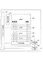
図2を参照して、撮像素子102の構成を説明する。図2は撮像素子102の一例を示すブロック図である。タイミング・パルス制御部201は、撮像素子102の各構成部に動作クロックを供給し、また各構成部にタイミング信号を供給することにより、撮像素子102の動作を制御する。垂直走査回路202は、画素部203から画素信号電圧を、1フレーム中に順次読出すタイミング制御を行う。一般的に、映像信号は1フレーム中に画素部203における上部の行から下部の行にかけて、行単位で順次読出される。
The configuration of the
画素部203は、多数の単位画素が2次元に配置された構成である。各単位画素は単数または複数の光電変換部を有しており、入射光量に応じて光電変換を行って電圧を出力する。フォトダイオード等の光電変換素子が用いられる。画素部203は通常の映像とともに位相差情報を取得して出力することもできる。例えば、1つのマイクロレンズに対してフォトダイオードが2つに分割された構造が挙げられる。画素部203は光電変換素子の他にフローティングディフュージョン部への電荷転送を行うトランジスタや、増幅トランジスタ等を備えるが、回路構成については公知であるので詳細な説明を省略する。
The
列アンプ204は、画素部203から列ごとに読出された信号を電気的に増幅する。列ADC205の前段に設けられた列アンプ204で信号を増幅することにより、列ADC205で発生するノイズに対してS/N比(信号対ノイズ比)を改善することができる。また列アンプ204においては、タイミング・パルス制御部201からの信号によって、アンプゲインを変更可能である。すなわち、撮像素子102は、HDR画像生成用として、列アンプ204のアンプゲインを変更して2種類のゲインで信号を出力することが可能である。列アンプ204は、光電変換部から出力された、ある時刻の信号に対して2つのゲインを乗算した信号を出力できるので、データ量は増えるものの、同時性を有する2つのゲインの異なる画像信号を取得できる。列アンプ204の構成については後述する。
The
列ADC(アナログ・デジタル変換部)205は、列アンプ204により増幅されたアナログ信号をデジタル信号に変換する。列メモリ209は、列ADC205によってデジタル化された画素からの出力信号を一時的に記憶しておく回路である。例えば列メモリ209に画素のノイズ信号を記憶しておき、所定のタイミングで水平転送回路206へ転送し、信号処理回路207で相関二重サンプリングの処理が行われる。相関二重サンプリングの処理は、ノイズ成分が含まれる画素信号からノイズ成分を減算することで両者の差分を算出し、ノイズ成分を除いた信号成分のみが取り出されるものである。
The column ADC (analog-to-digital converter) 205 converts the analog signal amplified by the
水平転送回路206は、列メモリ209に一時記憶されたデジタル信号を順次読出す処理を行う。水平転送回路206の出力は信号処理回路207に入力される。信号処理回路207はデジタル信号処理を行う回路である。信号処理回路207は、デジタル処理として、読出された画素信号からノイズ成分の信号を減算する相関二重サンプリングを行ったり、一定量のオフセット値の付加を行ったり、シフト演算や乗算を行う。また、信号処理回路207は、簡易的なゲイン演算を行うことができる。また、画素部203に意図的に遮光された画素領域が設けられている場合には、当該画素領域を利用したデジタル処理での黒レベルクランプ動作を行ってもよい。
The
外部出力回路208は信号処理回路207から信号を取得して出力処理を行う。外部出力回路208はシリアライザー機能を有し、信号処理回路207からの多ビットの入力パラレル信号をシリアル信号に変換する。また外部出力回路208は、このシリアル信号を、例えばLVDS信号等に変換して、外部デバイスに画像情報を出力する。
The
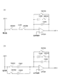
次に、HDR画像生成時の撮像素子102の動作について詳述する。本実施形態の撮像素子102は、HDR画像を生成するために列アンプ204のゲインを変更して出力することができる。図3(A)を参照して、HDR画像生成時の列アンプ204およびその周辺の回路例を説明する。図3(A)は、列アンプ204における、ある1列を抜き出して示す回路図である。容量部をCと表記し、スイッチ素子(トランジスタ等)をSWと表記し、オペアンプをOPと表記する。画素部203に繋がる垂直信号線は電流源に接続され、図3では左側の直線で示している。
Next, the operation of the
OP301には入力容量と帰還容量が接続されている。OP301の非反転入力端子には基準電源の電圧が印加され、反転入力端子はSW302、C301、SW301を介して垂直信号線に接続可能である。つまり、SW301およびSW302がオンのときに、画素部203から読出された信号が、入力容量であるC301を介してOP301に入力される。
An input capacitance and a feedback capacitance are connected to OP301. The voltage of the reference power supply is applied to the non-inverting input terminal of OP301, and the inverting input terminal can be connected to the vertical signal line via SW302, C301, and SW301. That is, when SW301 and SW302 are on, the signal read from the
C302とC303は帰還容量であり、SW303によってC302の接続および非接続を制御することができる。C303はその一端部がOP301の反転入力端子に接続され、他端部がOP301の出力端子に接続されている。C302およびSW303は、C303に対して並列に接続されている。C302とSW303とは直列に接続されており、C302の一端部がOP301の反転入力端子に接続され、他端部がSW303を介してOP301の出力端子に接続されている。リセット用のSW304は、C303と、C302およびSW303に対して、並列に接続されている。 C302 and C303 are feedback capacitances, and SW303 can control the connection and disconnection of C302. One end of C303 is connected to the inverting input terminal of OP301, and the other end is connected to the output terminal of OP301. C302 and SW303 are connected in parallel with C303. C302 and SW303 are connected in series, one end of C302 is connected to the inverting input terminal of OP301, and the other end is connected to the output terminal of OP301 via SW303. The reset SW304 is connected to C303 and C302 and SW303 in parallel.
列アンプ204の増幅率は、C301の静電容量と、C302およびC303の合成容量またはC303の静電容量との比の値によって決定され、「入力容量/帰還容量」から算出される。図3(A)では1つの入力容量に対して2つの帰還容量の組み合わせにより、2種類のゲインが得られる。つまり、異なるゲインを乗算した2枚の画像の信号を、後段の列ADC205へ出力することができる。
The amplification factor of the
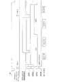
図4は、ゲインの異なる2枚の画像の信号を読出す動作を説明するタイミングチャートである。HDは水平同期信号を表す。撮像素子102の、ある行の読出しに着目して説明する。FD(フローティングディフュージョン)リセットは、各単位画素が備える光電変換部(フォトダイオード)およびFD部のリセットのタイミングを示す。その下には画素部203からの画素信号の転送タイミングと、各スイッチ素子の状態、列ADC205への出力をそれぞれ示す。
FIG. 4 is a timing chart illustrating an operation of reading signals of two images having different gains. HD represents a horizontal sync signal. The description will be given focusing on the reading of a certain line of the
読出し対象画素の光電変換部(フォトダイオード)およびFD部がリセットされるとともに、OP301の周辺回路の全スイッチ素子がONになり、残留電荷を排出するリセット動作が行われる。次に図3(A)のSW301、SW302をONとし、第1のゲインであるGain1で画素部203からのノイズ成分(ノイズ信号ともいう)を読出す処理が行われる。このとき、SW303はOFFとなっている。よって、第1のゲインをGain1と表記すると、
Gain1=C301/C303
で決定される。列ADC205に対し、第1のゲインで増幅されたノイズ信号(Gain1−Nと記す)が出力される。
The photoelectric conversion unit (photodiode) and FD unit of the pixel to be read are reset, and all the switch elements of the peripheral circuit of OP301 are turned on, and the reset operation of discharging the residual charge is performed. Next, SW301 and SW302 of FIG. 3A are turned ON, and a process of reading a noise component (also referred to as a noise signal) from the
Gain1 = C301 / C303
Is determined by. A noise signal (denoted as Gain1-N) amplified by the first gain is output to the column ADC205.
次に画素部203からの画素信号を列アンプ204に転送する処理が行われる。このとき、SW301、SW302をONとし、まず第1のゲインであるGain1で画素信号を読出す処理が行われる。このとき、SW303はOFFとなっている。列ADC205に対し、第1のゲインで増幅された画素信号成分(Gain1−Sと記す)が出力される。ここで、SW301をOFFとすることで信号レベルの変動を抑制し、列ADC205でのアナログ・デジタル変換に影響を与えないようにすることができる。このときの画素信号にはノイズ成分も含まれている。
Next, a process of transferring the pixel signal from the
次に、SW303をONとして画素信号を読出す処理が行われる。このとき、第2のゲインをGain2と表記すると、
Gain2=C301/(C302+C303)
で決定される。右辺の分母はC302とC303との合成容量である。そして、列ADC205に対し、第2のゲインで増幅された画素信号成分(Gain2−Sと記す)が出力される。
Next, a process of reading the pixel signal with SW303 turned ON is performed. At this time, if the second gain is expressed as Gain2,
Gain2 = C301 / (C302 + C303)
Is determined by. The denominator on the right side is the combined capacitance of C302 and C303. Then, the pixel signal component (denoted as Gain2-S) amplified by the second gain is output to the
この例では、ゲインの異なる2つの信号を読出す方法として、SW303をOFFに制御したGain1の状態を先に発生させ、その後にSW303をONに制御したGain2の状態を発生させている。図4の動作とは逆に、Gain2で増幅した信号から先に読出すことも可能である。本実施形態では、画素信号成分とノイズ成分を読出す際、FDリセット直後のゲインをGain1とし、その後のゲインをGain2とする。すなわち、「Gain1>Gain2」としており、相対的に大きいゲインでノイズや画素信号が読出された後に、相対的に小さいゲインで画素信号が読出される。 In this example, as a method of reading two signals having different gains, the state of Gain1 in which SW303 is controlled to OFF is first generated, and then the state of Gain2 in which SW303 is controlled to ON is generated. Contrary to the operation of FIG. 4, it is also possible to read the signal amplified by Gain 2 first. In the present embodiment, when reading out the pixel signal component and the noise component, the gain immediately after the FD reset is set to Gain 1, and the gain thereafter is set to Gain 2. That is, "Gain1> Gain2" is set, and after the noise and the pixel signal are read out with a relatively large gain, the pixel signal is read out with a relatively small gain.
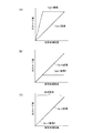
次に図5を参照して、画像合成部104により行われる2種類のゲインで読出された信号の合成方法の例を示す。図5(A)は、横軸に被写体の輝度値を示し、縦軸に撮像素子内のデジタル変換値、すなわち撮像素子102からの出力コード値を示すグラフである。Gain1で読出された信号に基づく画像(以下、Gain1画像という)については点線の折れ線グラフで表す。また、Gain2で読出された信号に基づく画像(以下、Gain2画像という)については実線の直線グラフで表す。
Next, with reference to FIG. 5, an example of a method of synthesizing signals read with two types of gains performed by the
「Gain1>Gain2」の関係であるため、Gain2画像を表すグラフはGain1画像を表すグラフよりも傾きが小さい。一方、Gain1画像については列アンプ204のゲインが大きいので、Gain2画像よりも被写体の輝度が小さいところで、出力コード値が飽和上限値(最大値)に到達してしまうが、暗部のノイズに関してGain2画像よりも良好である。
Since the relationship is "Gain1> Gain2", the graph representing the Gain2 image has a smaller slope than the graph representing the Gain1 image. On the other hand, since the gain of the
図5(B)は、デジタルゲイン等で、Gain1画像を表すグラフの傾きを、Gain2画像を表すグラフの傾きに合わせる処理を説明するグラフである。横軸および縦軸の設定については図5(A)と同じである。Gain1画像を表すグラフに対して調整処理を行った後のグラフを、点線の折れ線グラフで示しており、このときの画像を「Gain1画像2」とする。低輝度側の所定領域において、折れ線グラフの直線部の傾きは、Gain2画像を表す直線グラフの傾きと一致している。図5(A)と比較して、Gain1画像2の出力コードの最大値は小さくなる。 FIG. 5B is a graph for explaining a process of adjusting the slope of the graph representing the Gain1 image to the slope of the graph representing the Gain2 image by digital gain or the like. The settings of the horizontal axis and the vertical axis are the same as those in FIG. 5 (A). The graph after the adjustment processing is performed on the graph representing the Gain1 image is shown as a dotted line graph, and the image at this time is referred to as "Gain1 image 2". In the predetermined region on the low-luminance side, the slope of the straight line portion of the line graph coincides with the slope of the straight line graph representing the Gain2 image. Compared with FIG. 5A, the maximum value of the output code of Gain1 image 2 is smaller.
図5(C)は、画像合成処理を説明するグラフであり、横軸および縦軸の設定については図5(A)と同じである。画像合成では、低輝度側の領域においてGain1画像2を表すグラフの飽和部までは、Gain1画像2の出力コードが用いられる(点線参照)。当該領域よりも輝度の高い領域(つまりGain1画像2の出力コードが一定値となる領域)では、Gain2画像の出力コードが用いられる。つまり、暗部ではGain1画像2(ノイズが小さい画像)を用い、明部ではGain2画像(輝度が明るい被写体の情報を含む)を用いて合成画像を生成することでDR拡大が行われる。なお、図5で示した画像合成方法は一例であり、Gain1画像2とGain2画像との切り替えによって2枚の画像をブレンドする方法等、各種方法での実施が可能である。 FIG. 5C is a graph for explaining the image composition process, and the settings of the horizontal axis and the vertical axis are the same as those of FIG. 5A. In the image composition, the output code of the Gain1 image 2 is used up to the saturated portion of the graph representing the Gain1 image 2 in the low-luminance side region (see the dotted line). In a region having higher brightness than the region (that is, a region where the output code of the Gain1 image 2 is a constant value), the output code of the Gain2 image is used. That is, DR enlargement is performed by generating a composite image using a Gain1 image 2 (an image with low noise) in a dark portion and a Gain2 image (including information on a subject having a bright brightness) in a bright portion. The image composition method shown in FIG. 5 is an example, and can be carried out by various methods such as a method of blending two images by switching between the Gain1 image 2 and the Gain2 image.
本実施形態では、信号処理回路207において、第1のゲインの画素信号から第1のゲインのノイズ成分の信号を減算する相関二重サンプリングが行われる。このような相関二重サンプリングが行われるノイズ信号と画素信号を読出すときに用いる第1のゲインの値を、画素信号のみを読出すときに用いる第2のゲインの値よりも大きく設定する。これにより、画像の暗部に使用される第1のゲインの画素信号のノイズ特性を確実に改善して、ダイナミックレンジを拡大することができる。なお、本実施形態で示した回路構成は一例である。同一の画素信号に対して複数のゲインを乗算して出力することが可能な構成であれば如何なる回路構成でもよく、本実施形態にて図示した構成に限定されるものではない。例えば、FD部への付加容量の接続と非接続を制御することによりゲインの変更を行う方法等がある。
In the present embodiment, in the
[第2実施形態]
次に本発明の第2実施形態を説明する。本実施形態では、撮像素子から第2のゲインであるGain2で増幅されたノイズ信号(以下、Gain2−Nと記す)を出力して撮像素子の外部で処理する例を説明する。本実施形態において第1実施形態と同様の事項については既に使用した符号や記号を使用することによって、それらの説明を省略し、相違点を説明する。このような説明の省略方法は後述の実施形態でも同じである。
[Second Embodiment]
Next, a second embodiment of the present invention will be described. In the present embodiment, an example will be described in which a noise signal amplified by Gain2 (hereinafter referred to as Gain2-N), which is a second gain, is output from the image pickup device and processed outside the image pickup device. In the present embodiment, the same items as those in the first embodiment will be described by omitting the description thereof and explaining the differences by using the symbols and symbols already used. The method of omitting such a description is the same in the embodiments described later.
図6は、異なるゲインが乗算された2つのS信号と、Gain1−Nに加え、さらにGain2−Nを読出す動作について説明するタイミングチャートである。Gain1−N、Gain1−S、Gain2−Sを読出す動作は、図4と同じである。 FIG. 6 is a timing chart illustrating two S signals multiplied by different gains and an operation of reading Gain2-N in addition to Gain1-N. The operation of reading Gain1-N, Gain1-S, and Gain2-S is the same as in FIG.
Gain2−Sの読出し後に、Gain2−Nの読出しを行うために、もう一度FDリセットと、SW304のONによる列アンプ204のリセットが行われる。このリセット後に、SW303がON状態のままで、Gain2−Nの読出しが行われる。
After reading Gain2-S, the FD is reset again and the
その後、信号処理回路207において、Gain1−SからGain1−Nを減算することにより、第1のゲインで増幅された信号の相関二重サンプリングを行う。さらに、Gain2−SからGain2−Nを減算することにより、第2のゲインで増幅された信号の相関二重サンプリングを行う。ここで、本実施形態では、Gain2−Nを読出す前に一度FDリセットを行っているため、第2のゲインで増幅された信号については厳密には相関二重サンプリングの効果は得られない。しかしながら、Gain2−Nを読み出すことでGain2−Sに含まれるノイズ成分の概算値を取得できるため、例えば、画像合成時に画像信号の黒レベルを合わせる処理やノイズ除去または低減処理等に効果がある。
Then, in the
本実施形態のように、フォトダイオードおよびFD部のリセット後に、擬似的にGain2−Nを読出す駆動を行う場合にも、「Gain1>Gain2」とすることで、合成画像における暗部のノイズ特性を改善し、DR拡大を行うことができる。さらに、Gain2−Nを読出して、擬似的な相関二重サンプリングを行うことで、Gain1画像2とGain2画像との合成を行う際、Gain2画像の黒レベルを合わせることができ、合成が容易となる。 Even when driving to read Gain2-N in a pseudo manner after resetting the photodiode and the FD unit as in the present embodiment, the noise characteristics of the dark part in the composite image can be improved by setting “Gain1> Gain2”. It can be improved and DR expansion can be performed. Further, by reading Gain2-N and performing pseudo correlated double sampling, when synthesizing the Gain1 image 2 and the Gain2 image, the black level of the Gain2 image can be matched, and the composition becomes easy. ..
本実施形態によれば、再度フォトダイオードおよびFD部のリセットを行うことで、第1のゲインと第2のゲインのいずれについてもノイズ信号と画素信号を読出すことができる。 According to the present embodiment, by resetting the photodiode and the FD unit again, the noise signal and the pixel signal can be read out for both the first gain and the second gain.
[第3実施形態]
次に本発明の第3実施形態を説明する。本実施形態では画素信号の読出し前に、Gain1およびGain2でノイズ信号をそれぞれ読出す例を示す。
[Third Embodiment]
Next, a third embodiment of the present invention will be described. In this embodiment, an example in which the noise signal is read out by Gain1 and Gain2, respectively, before reading out the pixel signal is shown.
図3(B)は、本実施形態に係る列アンプ204において、ある1列を抜き出して示す回路図である。本実施形態では図3(A)に示す構成に加え、スイッチ素子SW302と入力容量C304が追加されている。つまり、OP301の入力段において、SW301とC301との直列回路に対して、SW302とC304との直列回路が並列に接続されている。
FIG. 3B is a circuit diagram showing one row extracted from the
図7は、本実施形態におけるゲインの異なる2枚の画像の信号を読出す動作を説明するタイミングチャートである。図7を参照して、異なるゲインで画素信号(S信号)およびノイズ信号(N信号)を読出す処理を説明する。まず、読出し対象画素のフォトダイオードおよびFD部がリセットされるとともに、OP301の周辺回路の全スイッチ素子がONになり、残留電荷を排出するリセット動作が行われる。その後、SW301がONであって、SW302、SW303はともにOFFの状態にする。この状態でのゲインは、
Gain2=C301/C303
となる。この状態で画素部302から画素信号の転送は行われず、Gain2−Nが読出される。
FIG. 7 is a timing chart illustrating an operation of reading signals of two images having different gains in the present embodiment. A process of reading a pixel signal (S signal) and a noise signal (N signal) with different gains will be described with reference to FIG. 7. First, the photodiode and FD portion of the pixel to be read are reset, and all the switch elements of the peripheral circuit of OP301 are turned on, and the reset operation of discharging the residual charge is performed. After that, SW301 is turned on, and both SW302 and SW303 are turned off. The gain in this state is
Gain2 = C301 / C303
Will be. In this state, the pixel signal is not transferred from the pixel unit 302, and Gain2-N is read out.
次にSW302がONとなり、Gain1の状態になる。この状態でのゲインは、
Gain1=(C301+C304)/C303
となる。この状態でGain1−Nが読出される。
Next, SW302 is turned on and the state of Gain1 is reached. The gain in this state is
Gain1 = (C301 + C304) / C303
Will be. Gain1-N is read in this state.
続いてGain1の状態のままで、画素部203から画素信号の転送が行われ、Gain1−Sが読出される。次にSW303がONとなり、Gain2の状態になる。この状態でのゲインは、
Gain2=(C301+C304)/(C302+C303)
となる。この状態でGain2−Sが読出される。本実施形態では、「C301/C303」から決定されるゲインと、「(C301+C304)/(C302+C303)」から決定されるゲインとが同等になるように静電容量が設定されている。
Subsequently, in the state of Gain1, the pixel signal is transferred from the
Gain2 = (C301 + C304) / (C302 + C303)
Will be. Gain2-S is read in this state. In the present embodiment, the capacitance is set so that the gain determined from "C301 / C303" and the gain determined from "(C301 + C304) / (C302 + C303)" are equivalent.
このようにして、Gain1とGain2でのN信号とS信号がそれぞれ読出される。相関二重サンプリングを行うためには、Gain2−Sを読出すまで、Gain2−Nを列メモリ209に保持しておく必要がある。
In this way, the N signal and the S signal in Gain1 and Gain2 are read out, respectively. In order to perform the correlated double sampling, it is necessary to hold the Gain2-N in the
図7に示すように、Gain2−NとGain2−Sとの間に、フォトダイオードおよびFD部のリセットは行われないが、Gain1−NとGain1−Sを読出す時間分に対応する期間が発生する。第2実施形態と同様に、ノイズ成分の概算値を読出すことができるので、画像合成時に画像信号の黒レベルを合わせる処理やノイズ除去または低減処理等に効果がある。 As shown in FIG. 7, the photodiode and the FD unit are not reset between Gain2-N and Gain2-S, but a period corresponding to the time for reading Gain1-N and Gain1-S occurs. do. Since the approximate value of the noise component can be read out as in the second embodiment, it is effective in the process of adjusting the black level of the image signal at the time of image composition, the noise removal or reduction process, and the like.
「Gain1>Gain2」とすることで、合成画像における暗部のノイズ特性を改善し、DR拡大を行うことができる。さらに、Gain2−Nを読出して、擬似的な相関二重サンプリングを行うことで、Gain1画像2とGain2画像との合成を行う際、Gain2画像の黒レベルを合わせることができ、合成が容易となる。本実施形態では、列メモリ209の構成を変更し、Gain2−Sを読出すまでの間、Gain2−Nを保持しておくことで、第1のゲインと第2のゲインのいずれについてもノイズ信号と画素信号を読出すことができる。
By setting "Gain1> Gain2", it is possible to improve the noise characteristics of the dark part in the composite image and perform DR enlargement. Further, by reading Gain2-N and performing pseudo correlated double sampling, when synthesizing the Gain1 image 2 and the Gain2 image, the black level of the Gain2 image can be matched, and the composition becomes easy. .. In the present embodiment, by changing the configuration of the
本実施形態の信号読出し方法のほかには、FDリセットとオペアンプの帰還容量部のリセットを行う方法がある。この方法ではFDリセット後にC301とC304に電荷が保持されて、Gain1−N、Gain1−Sの順に読出される。その後、OP301の帰還容量部がリセットされてから、Gain2−N、Gain2−Sの順に読出される。 In addition to the signal reading method of the present embodiment, there is a method of resetting the FD and resetting the feedback capacitance portion of the operational amplifier. In this method, after the FD is reset, the electric charges are held in C301 and C304, and are read out in the order of Gain1-N and Gain1-S. After that, after the feedback capacitance portion of OP301 is reset, it is read in the order of Gain2-N and Gain2-S.
[第4実施形態]
次に本発明の第4実施形態を説明する。本実施形態では、第2実施形態と同様に、図3(A)の回路図で表される列アンプ204を用いる。第2実施形態では、Gain2−Nを読出す場合、フォトダイオードおよびFD部のリセットと列アンプ204のリセットとを行っている。一方、本実施形態の例では、Gain2−Nを読出す場合、フォトダイオードおよびFD部のリセットのみを行い、列アンプ204のリセットを行わない。
[Fourth Embodiment]
Next, a fourth embodiment of the present invention will be described. In the present embodiment, as in the second embodiment, the
図8は、本実施形態における読出し動作を説明するタイミングチャートである。図8を参照して、異なるゲインで画素信号(S信号)およびノイズ信号(N信号)を読出す処理を説明する。 FIG. 8 is a timing chart for explaining the reading operation in the present embodiment. A process of reading a pixel signal (S signal) and a noise signal (N signal) with different gains will be described with reference to FIG.
まず、Gain2−Sを読出すまでの動作は、SW301の動作以外は、図6に示す第2実施形態の動作と同様である。本実施形態では、画素信号の変化時に、SW301を一時的にOFFにする。このように、画素信号の変化時にSW301を一時的にOFFにすることで、画素転送時やFDリセット時のFDノードの変動の影響を低減することができる。 First, the operation until reading Gain2-S is the same as the operation of the second embodiment shown in FIG. 6, except for the operation of SW301. In the present embodiment, the SW301 is temporarily turned off when the pixel signal changes. In this way, by temporarily turning off the SW301 when the pixel signal changes, it is possible to reduce the influence of the fluctuation of the FD node at the time of pixel transfer or FD reset.
FDノードの変動は、列アンプ204で増幅され、列アンプ204の動作点を大きく変動させる。すると、列アンプ204の回路動作の収束に時間を要するようになるため、回路の高速動作に影響を与える。なお、画素信号の変化時にSW301を一時的にOFFすることは、他の実施形態にも適用可能である。
The fluctuation of the FD node is amplified by the
Gain2−Sを読出した後、Gain2−Nを読出すために、一度、フォトダイオードおよびFDリセットを行う。このタイミングにおいて、本実施形態では、第2実施形態と異なり、SW301をOFFにする一方で列アンプ204のリセットを行わない。その後、Gain2でノイズ成分を読出すために、SW301をONにしてGain2−Nを読出す。これについてさらに説明する。
After reading Gain2-S, the photodiode and FD reset are performed once to read Gain2-N. At this timing, in the present embodiment, unlike the second embodiment, the SW301 is turned off while the
列アンプ204のアンプゲインを、SW303を制御してGain1からGain2に切り替える時に、SW303を制御したときのノイズが、列アンプ入力ノード(OP301の−入力端子)に入力されることがある。仮に、列アンプ204のアンプゲインのリセットを行って、Gain2−Nを読出すと、SW303によるノイズの影響を受けたS信号(Gain2−S)とSW303のノイズの影響を受けていないN信号(Gain2−N)を読出すことになる。すると、S信号とN信号の相関がさらに崩れる。S信号とN信号の相関が崩れると、例えば、水平方向のシェーディングが悪化するなど画質劣化に影響を与えることになる。
When the amplifier gain of the
本実施形態では、Gain2−Nを列アンプ204のアンプゲインをリセットせずに読出す。このように、Gain2−Nを読出すときに、列アンプ204のアンプゲインのリセットを行わないことで、Gain1、Gain2ともに画質劣化させることなくノイズ信号と画素信号を読出すことができる。なお、このとき、SW301は、本実施形態のようにOFFにすることが望ましい。
In this embodiment, Gain2-N is read out without resetting the amplifier gain of the
なお、本実施形態においては、前述の実施形態で示す「Gain1>Gain2」のように、Gain1がGain2よりも大きいこととしている。しかしながら、これに限るものではなく、Gain1がGain2よりも小さいこととしてもよい。 In this embodiment, Gain1 is larger than Gain2 as in "Gain1> Gain2" shown in the above-described embodiment. However, the present invention is not limited to this, and Gain1 may be smaller than Gain2.
前記実施形態によれば、増幅手段のゲインを変更して出力可能な撮像素子において、一般的にノイズが目立ちやすい低輝度部の画像のランダムノイズを低減するとともに、画像信号の黒レベルを決定することができる。合成後の画像信号のダイナミックレンジを拡大することができる。 According to the above embodiment, in an image sensor capable of outputting by changing the gain of the amplification means, the random noise of the image in the low-luminance portion where noise is generally conspicuous is reduced, and the black level of the image signal is determined. be able to. The dynamic range of the combined image signal can be expanded.
102・・・撮像素子
103・・・画像取得部
104・・・画像合成部
105・・・信号処理部
107・・・露出制御部
108・・・撮像素子制御部
102 ...
Claims (12)
前記増幅手段のゲインを制御する制御手段と、
前記増幅手段により増幅された画素信号からノイズ信号を減算する信号処理手段と、を備え、
前記制御手段は、前記画素部をリセットした後、前記増幅手段による第1のゲインでノイズ信号と画素信号を読出した後に、前記増幅手段による第2のゲインで画素信号を読出す制御を行い、
前記第1のゲインは、前記第2のゲインよりも大きい
ことを特徴とする撮像素子。 Amplification means that amplifies each signal from the photoelectric conversion unit of the pixel unit with a plurality of gains,
A control means for controlling the gain of the amplification means and
A signal processing means for subtracting a noise signal from a pixel signal amplified by the amplification means is provided.
The control means controls to read out the noise signal and the pixel signal with the first gain by the amplification means after resetting the pixel portion, and then read out the pixel signal with the second gain by the amplification means.
An image pickup device characterized in that the first gain is larger than the second gain.
ことを特徴とする請求項1に記載の撮像素子。 The first aspect of claim 1 is characterized in that the control means reads a pixel signal with the second gain, resets the pixel portion again, and then reads a noise signal with the second gain. Image sensor.
ことを特徴とする請求項1に記載の撮像素子。 The first aspect of claim 1, wherein the control means controls to read the noise signal at the second gain after resetting the pixel unit, and then read the noise signal at the first gain. Image sensor.
ことを特徴とする請求項3に記載の撮像素子。 The image pickup device according to claim 3, further comprising a storage means for holding the noise signal read by the second gain until the pixel signal is read by the second gain.
前記増幅手段のゲインを制御する制御手段と、
前記増幅手段により増幅された画素信号からノイズ信号を減算する信号処理手段と、を備え、
前記制御手段は、
前記画素部をリセットした後、前記増幅手段による第1のゲインでノイズ信号と画素信号を読出した後に、前記増幅手段による第2のゲインで画素信号を読出す制御を行い、前記第2のゲインで画素信号を読出した後、前記画素部を再びリセットした後に前記第2のゲインでノイズ信号を読出す制御を行う
ことを特徴とする撮像素子。 Amplification means that amplifies each signal from the photoelectric conversion unit of the pixel unit with a plurality of gains,
A control means for controlling the gain of the amplification means and
A signal processing means for subtracting a noise signal from a pixel signal amplified by the amplification means is provided.
The control means
After resetting the pixel portion, the noise signal and the pixel signal are read by the first gain by the amplification means, and then the pixel signal is read out by the second gain by the amplification means, and the second gain is read. An image pickup device characterized in that, after reading a pixel signal in, the pixel portion is reset again, and then the noise signal is read out with the second gain.
ことを特徴とする請求項5に記載の撮像素子。 The image pickup device according to claim 5, wherein the first gain is larger than the second gain.
ことを特徴とする請求項5に記載の撮像素子。 The image pickup device according to claim 5, wherein the first gain is smaller than the second gain.
前記画素部を再びリセットする際に、前記スイッチをオフにする
ことを特徴とする請求項5に記載の撮像素子。 A switch is provided between the pixel unit and the amplification means.
The image pickup device according to claim 5, wherein the switch is turned off when the pixel portion is reset again.
ことを特徴とする撮像装置。 An image pickup apparatus comprising the image pickup device according to any one of claims 1 to 8.
ことを特徴とする請求項9に記載の撮像装置。 The image pickup apparatus according to claim 9, further comprising a synthesis means for acquiring a plurality of signals amplified with different gains by the amplification means and synthesizing an image.
前記光電変換部からの信号ごとに増幅を行う増幅手段のゲインを制御する工程と、
前記画素部をリセットした後、前記増幅手段による第1のゲインでノイズ信号と画素信号を読出した後に前記増幅手段による第2のゲインで画素信号を読出す制御を行う工程と、
読出された画素信号からノイズ信号を減算する工程と、を有し、
前記第1のゲインは前記第2のゲインよりも大きい
ことを特徴とする撮像素子の制御方法。 A control method in which the pixel unit is executed by an image sensor having a photoelectric conversion unit.
A step of controlling the gain of the amplification means that amplifies each signal from the photoelectric conversion unit, and
A step of resetting the pixel portion, reading the noise signal and the pixel signal with the first gain by the amplification means, and then performing control to read the pixel signal with the second gain by the amplification means.
It has a step of subtracting a noise signal from the read pixel signal.
A method for controlling an image sensor, wherein the first gain is larger than the second gain.
前記光電変換部からの信号ごとに増幅を行う増幅手段のゲインを制御する工程と、
前記画素部をリセットした後、前記増幅手段による第1のゲインでノイズ信号と画素信号を読出した後に前記増幅手段による第2のゲインで画素信号を読出す制御を行う工程と、
前記第2のゲインで画素信号を読出した後、前記画素部を再びリセットした後に前記第2のゲインでノイズ信号を読出す制御を行う工程と、
読出された画素信号からノイズ信号を減算する工程と、を有する
ことを特徴とする撮像素子の制御方法。
A control method in which the pixel unit is executed by an image sensor having a photoelectric conversion unit.
A step of controlling the gain of the amplification means that amplifies each signal from the photoelectric conversion unit, and
A step of resetting the pixel portion, reading the noise signal and the pixel signal with the first gain by the amplification means, and then performing control to read the pixel signal with the second gain by the amplification means.
A step of reading a pixel signal with the second gain, resetting the pixel portion again, and then controlling the reading of a noise signal with the second gain.
A control method for an image pickup device, which comprises a step of subtracting a noise signal from a read pixel signal.
Priority Applications (1)
| Application Number | Priority Date | Filing Date | Title |
|---|---|---|---|
| US16/844,365 US11165978B2 (en) | 2019-04-16 | 2020-04-09 | Imaging device, control method thereof, and imaging apparatus |
Applications Claiming Priority (4)
| Application Number | Priority Date | Filing Date | Title |
|---|---|---|---|
| JP2019077811 | 2019-04-16 | ||
| JP2019077811 | 2019-04-16 | ||
| JP2020002564 | 2020-01-10 | ||
| JP2020002564 | 2020-01-10 |
Publications (2)
| Publication Number | Publication Date |
|---|---|
| JP2021106375A true JP2021106375A (en) | 2021-07-26 |
| JP2021106375A5 JP2021106375A5 (en) | 2023-03-13 |
Family
ID=76918980
Family Applications (1)
| Application Number | Title | Priority Date | Filing Date |
|---|---|---|---|
| JP2020046146A Pending JP2021106375A (en) | 2019-04-16 | 2020-03-17 | Image pick-up device and method for controlling the same, and imaging apparatus |
Country Status (1)
| Country | Link |
|---|---|
| JP (1) | JP2021106375A (en) |
-
2020
- 2020-03-17 JP JP2020046146A patent/JP2021106375A/en active Pending
Similar Documents
| Publication | Publication Date | Title |
|---|---|---|
| JP7353783B2 (en) | Imaging device and its control method; Imaging device and its control method | |
| JP5784426B2 (en) | Imaging device | |
| JP4311181B2 (en) | Semiconductor device control method, signal processing method, semiconductor device, and electronic apparatus | |
| JP2008219293A (en) | Imaging device and imaging system | |
| JP2009177749A (en) | Solid-state imaging apparatus | |
| JP5019705B2 (en) | Solid-state imaging device and driving method of solid-state imaging device | |
| US11165978B2 (en) | Imaging device, control method thereof, and imaging apparatus | |
| US9979910B2 (en) | Image capturing apparatus and control method thereof, and storage medium | |
| JP2008042298A (en) | Solid-state image pickup device | |
| JP2010245891A (en) | Imaging device and imaging method | |
| JP4419675B2 (en) | Solid-state imaging device and driving method of solid-state imaging device | |
| JP2007074435A (en) | Solid-state imaging device and its drive method | |
| US10560653B2 (en) | Image sensing apparatus and control method for performing analog-to-digital conversion | |
| JP5168319B2 (en) | Solid-state imaging device and driving method of solid-state imaging device | |
| JP2009218665A (en) | Solid-state image pickup element | |
| JP2008300898A (en) | Solid state imaging device and imaging system employing it | |
| JP2011151549A (en) | Signal processing apparatus, imaging device, and signal processing method | |
| JP4916095B2 (en) | Solid-state imaging device and driving method of solid-state imaging device | |
| JP2020115604A (en) | Imaging apparatus and control method of the same | |
| JP2020043391A (en) | Imaging apparatus and control method thereof | |
| JP6896788B2 (en) | Imaging equipment, imaging methods, computer programs and storage media | |
| JP2021106375A (en) | Image pick-up device and method for controlling the same, and imaging apparatus | |
| JP7236282B2 (en) | Image processing device and method, and imaging device | |
| JP2024057445A (en) | Imaging device and control method thereof | |
| KR100704758B1 (en) | Apparatus for correlating image signal of a CCD camera system |
Legal Events
| Date | Code | Title | Description |
|---|---|---|---|
| A521 | Request for written amendment filed |
Free format text: JAPANESE INTERMEDIATE CODE: A523 Effective date: 20230303 |
|
| A621 | Written request for application examination |
Free format text: JAPANESE INTERMEDIATE CODE: A621 Effective date: 20230303 |
|
| A977 | Report on retrieval |
Free format text: JAPANESE INTERMEDIATE CODE: A971007 Effective date: 20231129 |
|
| A131 | Notification of reasons for refusal |
Free format text: JAPANESE INTERMEDIATE CODE: A131 Effective date: 20231212 |