JP2021082003A - Information processing device - Google Patents
Information processing device Download PDFInfo
- Publication number
- JP2021082003A JP2021082003A JP2019208993A JP2019208993A JP2021082003A JP 2021082003 A JP2021082003 A JP 2021082003A JP 2019208993 A JP2019208993 A JP 2019208993A JP 2019208993 A JP2019208993 A JP 2019208993A JP 2021082003 A JP2021082003 A JP 2021082003A
- Authority
- JP
- Japan
- Prior art keywords
- storage device
- data
- communication means
- hdd
- sata
- Prior art date
- Legal status (The legal status is an assumption and is not a legal conclusion. Google has not performed a legal analysis and makes no representation as to the accuracy of the status listed.)
- Pending
Links
Images


Classifications
-
- G—PHYSICS
- G06—COMPUTING; CALCULATING OR COUNTING
- G06F—ELECTRIC DIGITAL DATA PROCESSING
- G06F3/00—Input arrangements for transferring data to be processed into a form capable of being handled by the computer; Output arrangements for transferring data from processing unit to output unit, e.g. interface arrangements
- G06F3/06—Digital input from, or digital output to, record carriers, e.g. RAID, emulated record carriers or networked record carriers
- G06F3/0601—Interfaces specially adapted for storage systems
- G06F3/0628—Interfaces specially adapted for storage systems making use of a particular technique
- G06F3/0655—Vertical data movement, i.e. input-output transfer; data movement between one or more hosts and one or more storage devices
-
- G—PHYSICS
- G06—COMPUTING; CALCULATING OR COUNTING
- G06F—ELECTRIC DIGITAL DATA PROCESSING
- G06F3/00—Input arrangements for transferring data to be processed into a form capable of being handled by the computer; Output arrangements for transferring data from processing unit to output unit, e.g. interface arrangements
- G06F3/06—Digital input from, or digital output to, record carriers, e.g. RAID, emulated record carriers or networked record carriers
- G06F3/0601—Interfaces specially adapted for storage systems
- G06F3/0668—Interfaces specially adapted for storage systems adopting a particular infrastructure
- G06F3/0671—In-line storage system
- G06F3/0683—Plurality of storage devices
- G06F3/0689—Disk arrays, e.g. RAID, JBOD
-
- G—PHYSICS
- G06—COMPUTING; CALCULATING OR COUNTING
- G06F—ELECTRIC DIGITAL DATA PROCESSING
- G06F3/00—Input arrangements for transferring data to be processed into a form capable of being handled by the computer; Output arrangements for transferring data from processing unit to output unit, e.g. interface arrangements
- G06F3/06—Digital input from, or digital output to, record carriers, e.g. RAID, emulated record carriers or networked record carriers
- G06F3/0601—Interfaces specially adapted for storage systems
- G06F3/0602—Interfaces specially adapted for storage systems specifically adapted to achieve a particular effect
- G06F3/061—Improving I/O performance
- G06F3/0611—Improving I/O performance in relation to response time
-
- G—PHYSICS
- G06—COMPUTING; CALCULATING OR COUNTING
- G06F—ELECTRIC DIGITAL DATA PROCESSING
- G06F3/00—Input arrangements for transferring data to be processed into a form capable of being handled by the computer; Output arrangements for transferring data from processing unit to output unit, e.g. interface arrangements
- G06F3/06—Digital input from, or digital output to, record carriers, e.g. RAID, emulated record carriers or networked record carriers
- G06F3/0601—Interfaces specially adapted for storage systems
- G06F3/0628—Interfaces specially adapted for storage systems making use of a particular technique
- G06F3/0655—Vertical data movement, i.e. input-output transfer; data movement between one or more hosts and one or more storage devices
- G06F3/0659—Command handling arrangements, e.g. command buffers, queues, command scheduling
-
- G—PHYSICS
- G06—COMPUTING; CALCULATING OR COUNTING
- G06F—ELECTRIC DIGITAL DATA PROCESSING
- G06F3/00—Input arrangements for transferring data to be processed into a form capable of being handled by the computer; Output arrangements for transferring data from processing unit to output unit, e.g. interface arrangements
- G06F3/06—Digital input from, or digital output to, record carriers, e.g. RAID, emulated record carriers or networked record carriers
- G06F3/0601—Interfaces specially adapted for storage systems
- G06F3/0668—Interfaces specially adapted for storage systems adopting a particular infrastructure
- G06F3/0671—In-line storage system
- G06F3/0673—Single storage device
- G06F3/0674—Disk device
- G06F3/0676—Magnetic disk device
-
- G—PHYSICS
- G06—COMPUTING; CALCULATING OR COUNTING
- G06F—ELECTRIC DIGITAL DATA PROCESSING
- G06F3/00—Input arrangements for transferring data to be processed into a form capable of being handled by the computer; Output arrangements for transferring data from processing unit to output unit, e.g. interface arrangements
- G06F3/06—Digital input from, or digital output to, record carriers, e.g. RAID, emulated record carriers or networked record carriers
- G06F3/0601—Interfaces specially adapted for storage systems
- G06F3/0668—Interfaces specially adapted for storage systems adopting a particular infrastructure
- G06F3/0671—In-line storage system
- G06F3/0673—Single storage device
- G06F3/0679—Non-volatile semiconductor memory device, e.g. flash memory, one time programmable memory [OTP]
Abstract
Description
本発明は、情報処理装置および情報処理装置の制御方法に関する。 The present invention relates to an information processing device and a control method for the information processing device.
印刷装置などの情報処理装置において、複数のストレージデバイス(以後、ストレージ)を搭載してミラーリング機能を実装しているものがある。ここでミラーリング機能とは、複数台のHDD(ハードディスクドライブ)やSSD(ソリッドステートドライブ)などのストレージの全てに同一アドレスから同サイズのデータを書き込む機能である。ミラーリング機能の制御は、ミラーリング制御を行うコントローラ(以下、コントローラ)によって行われる。 Some information processing devices such as printing devices are equipped with a plurality of storage devices (hereinafter referred to as storage) to implement a mirroring function. Here, the mirroring function is a function of writing data of the same size from the same address to all storages such as a plurality of HDDs (hard disk drives) and SSDs (solid state drives). The mirroring function is controlled by a controller that performs mirroring control (hereinafter referred to as a controller).
コントローラは、上流のホストコントローラから書き込み/読み出しの要求を受けると、ミラーリング制御している複数のストレージに受け付けた要求に応じた指示を出す。そして、コントローラは、ミラーリング機能で用いる複数のストレージの各々から応答を受け付けると、上流のホストコントローラに応答を返す。 When the controller receives a write / read request from the upstream host controller, the controller issues an instruction according to the received request to the plurality of storages under mirroring control. Then, when the controller receives a response from each of the plurality of storages used in the mirroring function, the controller returns the response to the upstream host controller.
コントローラは、例えば2つのストレージのうちすべてのストレージから正常に書き込み/読み出しが出来た旨の応答を受けた場合には、ホストコントローラに正常に書き込み/読み出しが出来た旨の応答を返す。また、例えば2つのストレージのうち一方のストレージから正常に書き込み/読み出しが出来た旨の応答を受け、他方のストレージからエラーになった旨の応答を受けた場合にも、ホストコントローラに正常に書き込み/読み出しが出来た旨の応答を返す。そして、例えば2つのストレージのうち両方のストレージからエラーになった旨の応答を受けた場合には、ホストコントローラにエラーになった旨の応答を返す。 For example, when the controller receives a response from all of the two storages that the write / read can be performed normally, the controller returns a response that the write / read can be performed normally to the host controller. Also, for example, when receiving a response from one of the two storages that a write / read was successful and receiving a response from the other storage that an error occurred, the host controller is normally written. / Returns a response that the reading was successful. Then, for example, when a response indicating that an error has occurred is received from both storages of the two storages, a response indicating that an error has occurred is returned to the host controller.
ミラーリング機能で用いる複数のストレージへの書き込み/読み出し速度は、ストレージごとに異なることがある。例えば、同一の種類のストレージ(HDD)を複数用いた場合には、一部のHDDの書き込み/読み出しの応答は早く、他部のHDDの書き込み/読み出しの応答は一部のHDDに比べて遅い場合(もしくは応答が帰って来ない場合)である。この事例は、例えばHDDの経年劣化や性能の差などによって生じる。また、特許文献1に示すように、ミラーリング構成としてHDDとSSDを混在で搭載した場合には、SSDからの書き込み/読み出しの応答は早く、HDDの書き込み/読み出しの応答が遅くなる。
The write / read speed to multiple storages used in the mirroring function may differ from storage to storage. For example, when multiple storages (HDDs) of the same type are used, the write / read response of some HDDs is fast, and the write / read response of other HDDs is slower than that of some HDDs. If (or if no response is returned). This case occurs, for example, due to aged deterioration of HDDs and differences in performance. Further, as shown in
ミラーリングを制御するコントローラは、複数のストレージに書き込みの指示/読み出しの指示を送ってから、所定時間がたってもコマンドを送ったすべてのストレージから応答が帰ってこない場合にホストコントローラにエラーが生じた旨の応答を行う。そのため、各々ストレージの応答速度の差が大きい場合や、応答を返さないストレージが存在した場合には、コントローラからの指示を正常に処理したストレージがあったとしても、コントローラは、ホストコントローラにエラーが生じた旨の応答を行ってしまう。 The controller that controls mirroring sent a write / read instruction to multiple storages, and then an error occurred in the host controller when no response was returned from all the storages that sent the command within a specified time. Make a response to that effect. Therefore, if there is a large difference in the response speed of each storage, or if there is a storage that does not return a response, even if there is a storage that normally processed the instruction from the controller, the controller will cause an error in the host controller. It responds to the effect that it has occurred.
そのためコマンドを送信したホストコントローラは、正常なストレージがあったとしても、すべてのストレージがエラー状態であると認識してしまうおそれがある。 Therefore, the host controller that sent the command may recognize that all the storage is in an error state even if there is normal storage.
本発明は、書き込みコマンドに対して所定時間内に応答がないストレージがある場合に、ミラーリングを制御するコントローラがホストコントローラにエラー状態であると誤認識させないことを目的とする。 An object of the present invention is to prevent the host controller from erroneously recognizing that the controller that controls mirroring is in an error state when there is a storage that does not respond to a write command within a predetermined time.
本発明は、不揮発性の第1記憶装置および不揮発性の第2記憶装置を有する情報処理装置であって、データの書き込み指示を受け付ける第1通信手段と、前記書き込み指示を前記第1記憶装置に送信する第2通信手段と、前記書き込み指示を前記第2記憶装置に送信する第3通信手段と、前記第2通信手段を介する前記第1記憶装置へのデータの送信および前記第3通信手段を介する前記第2記憶装置へのデータの送信を制御する制御手段と、
を有し、前記第1記憶装置から前記書き込み指示に対する応答を受け付け、且つ、前記第2記憶装置から前記書き込み指示に対する応答を受け付けないことに基づいて、前記制御手段は、前記第1記憶装置への前記データの送信を継続し、前記第2記憶装置への前記データの送信を停止し、前記第1記憶装置による前記データの記憶の完了通知を前記第2通信手段が受け付けることに基づいて、前記第1通信手段は、前記書き込み指示に対する処理の完了通知を送信することを特徴とする。
The present invention is an information processing device having a non-volatile first storage device and a non-volatile second storage device, the first communication means for receiving a data writing instruction, and the writing instruction to the first storage device. A second communication means for transmitting, a third communication means for transmitting the writing instruction to the second storage device, data transmission to the first storage device via the second communication means, and the third communication means. A control means for controlling the transmission of data to the second storage device via the device, and
The control means sends the control means to the first storage device based on the fact that the response to the write instruction is received from the first storage device and the response to the write instruction is not received from the second storage device. Based on the fact that the transmission of the data is continued, the transmission of the data to the second storage device is stopped, and the second communication means receives the completion notification of the storage of the data by the first storage device. The first communication means is characterized in that it transmits a processing completion notification in response to the writing instruction.
本発明は、書き込みコマンドに対して所定時間内に応答がないストレージがあったとしてもホストコントローラにすべてのストレージがエラー状態であると誤認識させないことが可能である。 According to the present invention, it is possible to prevent the host controller from erroneously recognizing that all the storages are in an error state even if some storages do not respond to the write command within a predetermined time.
(第1実施形態)
添付図面を参照して本実施形態の各実施例を詳しく説明する。以下の実施例は特許請求の範囲に係る発明を限定するものではなく、また各実施例で説明されている特徴の組み合わせすべてが発明の解決手段に必須の構成とは限らない。例えば、各実施例では、ミラーリング構成として2台のストレージデバイスとSATA‐IF(Serial Advanced Technology Attachment InterFace)を例として説明するが、この構成に限らない。ストレージデバイスが複数配された構成であれば何台でもよい。また、ストレージデバイスは、複数のHDDでもよいし、複数のSSDでもよいし、HDDとSSDが混在してもよい。なお、以下の実施例では、情報処理装置の例として画像処理装置を用いる。
(First Embodiment)
Each embodiment of the present embodiment will be described in detail with reference to the accompanying drawings. The following examples do not limit the invention according to the claims, and not all combinations of features described in each embodiment are essential configurations for the means of solving the invention. For example, in each embodiment, two storage devices and a SATA-IF (Serial Advanced Technology Interface) will be described as an example of a mirroring configuration, but the present invention is not limited to this configuration. Any number of storage devices may be used as long as they are arranged in a plurality of storage devices. Further, the storage device may be a plurality of HDDs, a plurality of SSDs, or a mixture of HDDs and SSDs. In the following examples, an image processing device is used as an example of the information processing device.
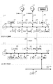
(実施例1)
図1は、画像処理装置におけるメインコントローラ120のシステム構成例である。メインCPU(中央処理演算器)101は、システム制御や各種演算処理を行う。メモリ制御部102は、各種メモリデバイスへの入出力制御やDMA(ダイレクト・メモリ・アクセス)制御を行う。
(Example 1)
FIG. 1 is an example of a system configuration of the
FLASHメモリ103は、書き換え可能な不揮発性メモリであり、システム全体の制御プログラムや制御パラメータ等が格納される。DRAM(ダイナミック・ランダム・アクセス・メモリ)104は、DDR(Double−Data−Rate)メモリに代表される揮発性の書き換え専用メモリである。プログラムの作業領域や印刷データの格納領域、各種テーブル情報格納領域等の用途に用いられる。ここで、メモリ制御部102と各種メモリデバイスとの関係は、簡略化して表現したものであって、一般的には独立に制御される。
The
LAN−IF制御部105は、印刷装置に接続されるローカル・エリア・ネットワーク106との入出力制御を行う。一般的にはTCP/IP(Transmission Control Protocol/Internet Protocol)プロトコルに対応する。ネットワークケーブルを介して外部HOSTコンピュータ107などのネットワーク対応機器と接続され、ネットワーク経由でのプリントを行うことができる。Reader‐IF制御部108は、スキャナ装置109との通信制御を行う。
The LAN-
スキャナ装置109によってスキャンした入力画像データを印字させることでコピー機能を実現する。画像処理部110は、LAN−IF制御部105、Reader‐IF制御部108を介して取り込んだ画像データに対して各種画像処理を行う。
The copy function is realized by printing the input image data scanned by the
SATAホスト制御部111(SATA回路)は、SATA規格に準拠したIFを有するデバイスとのデータ入出力制御を行う。SATAブリッジ制御部112(SATA回路)は、上流側としてSATAホスト制御部111にデバイスとして接続され、下流側としては複数のHost‐IFを有し、HDD又はSSD(ソリッドステートドライブ)113、114と接続される。SATAブリッジ制御部112では、RAID(Redundant Arrays of Inexpensive Disk)制御やデータ暗号化など付加価値としての機能が搭載されている。
The SATA host control unit 111 (SATA circuit) performs data input / output control with a device having an IF conforming to the SATA standard. The SATA bridge control unit 112 (SATA circuit) is connected to the SATA
本実施例では、SATAホスト制御部111とSATAブリッジ制御部112は、それぞれ独立したASIC(特定用途向け集積回路)としてメインコントローラ120に搭載されていることを前提として説明を行う。
In this embodiment, the SATA
パネルIF部115は、パネル装置116との通信制御を行う。ここでは図示しないがUI(ユーザー・インターフェイス)として、パネル上の液晶画面表示やボタン等を操作することにより印刷装置の各種設定及び状態の確認ができる。
The
ビデオ出力IF部117は、印刷部118とのコマンド/ステータスの通信制御や印刷データの転送を行う。印刷部118は、ここでは図示しないが印刷装置本体と給紙系及び排紙系から構成され、主にビデオ出力IF部117からのコマンド情報に従い、印刷データを用紙に印刷する。メインバス119はバスコントローラ含み、制御バス、データバス及び任意ブロック間のローカルバスを便宜的にまとめて表現したものである。代表例としてPCIe(PCI Express)やASICの内部バスなども含まれる。
The video
図2は、SATAブリッジ構成としての接続例を示す図である。メインASIC201は、SATAホスト制御部111を含むメインコントローラ120のシステム全体を制御する中心的なASICである。SATAホスト制御部111は、1個のSATA‐IP(Intellectual Property)202をホストIFとして持つ。サブASICは、SATAブリッジ制御部112そのものであり、メインコントローラ120上に独立したIC(Integrated Circuit)として実装されている。
FIG. 2 is a diagram showing a connection example as a SATA bridge configuration. The
SATAブリッジ制御部112は3個のSATA−IP203〜205を持つ。ブリッジ構成での上流側はSATA‐IP(Host)202がH‐Host‐IF206を介してSATA‐IP(Device)203と接続される。下流側はSATA‐IP(Host1)204がB‐Host1‐IF207を介してHDD113(SSDでもよい)と、SATA‐IP(Host2)205がB‐Host2‐IF208を介してHDD114(SSDでもよい)と接続される。
The SATA
ここで、SATA‐IP202〜205は、SATAリンク層及び物理層から構成される。そして、SATA‐IP202〜205は、各種SATAレジスタの設定に応じてSATA−IF206〜208で接続されるSATAデバイスに対して物理的な(電気信号としての)SATA規格のコマンド発行やステータス受信を行う。つまり、SATA‐IP202〜205は、通信部として機能する。 Here, SATA-IP202 to 205 are composed of a SATA link layer and a physical layer. Then, SATA-IP202 to 205 issue physical (as an electrical signal) SATA standard command and receive status to the SATA device connected by SATA-IF206 to 208 according to the setting of various SATA registers. .. That is, SATA-IP202 to 205 function as a communication unit.
また、SATAブリッジ制御部112は、電源制御部209と制御信号214で接続されている。電源制御部209はメインボード上に搭載され、メインコントローラ120に含まれる各機能モジュールやそれに接続される各種装置への電力供給の有無を決定し、印刷装置システム全体としての電源制御を担っている。
Further, the SATA
電源制御部209から出ている一点斜線210〜213は、システム全体の部分であるSATAブリッジ部の各構成要素にたいする電源ラインを示したものである。従って、制御信号214を介した電源制御部209とのやり取りによってSATAブリッジ制御部112は意図したタイミングでHDD113及び114の電源をOFF・ONすることが可能となる。
The one-point
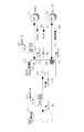
図3は、SATAホスト制御部111及びSATAブリッジ制御部112の内部構成例を示す図である。HCPU301は、SATAコマンド発行処理、送受信データの転送処理及びステータス受信処理等SATAコントローラとしての全般的な制御を行う。また、HCPU301は、メインバス119を介してメインコントローラ120に含まれるCPU101と通信を行う。
FIG. 3 is a diagram showing an example of internal configurations of the SATA
メモリ制御部302は、Flashメモリ303やSRAM(スタティック・ランダム・アクセス・メモリ)304との入出力制御を行う。Flashメモリ303には、ブートプログラムやSATAコントローラとしての制御プログラムが格納されている。SRAM304にはHCPU301の作業領域、各種制御テーブルやパラメータ格納領域及びデータバッファなどに使用される。ここで、SRAM304は1ポートRAM、2ポートRAM、FIFO(First‐IN First‐OUT)メモリ等の制御を簡略化して記載しているのであって、それぞれ独立に制御され複数個所にSRAMが存在しても構わない。
The
割り込み制御部305は、HCPU301に対する割り込み信号の入力や出力処理、割り込み信号に対するマスク処理などを行う。SATAブリッジ制御部112からの割り込み信号318も接続されている。レジスタH306は、制御パラメータやステータス情報などを一時的に記憶するためのレジスタである。DMAC(ダイレクト・メモリ・アクセス・コントローラ)307は、ここでは図示しないがHCPU301によって所定のレジスタに転送元及び転送先の先頭アドレス及びサイズが設定され、起動が掛けられると所定のメモリ間でデータ転送を行う。
The interrupt
Hバス308はバスコントローラ含み、制御バス、データバス及び任意ブロック間のローカルバスを便宜的にまとめて表現したものである。バスブリッジ回路309は、メインバス119とHバス308間のバスプロトコルを相互に変換するバスブリッジである。これによってDMAC307は、メインバス119に接続されているメインコントローラ120に含まれるDRAM104にアクセスすることが可能となる。
The
BCPU310は、SATAコマンド発行処理、送受信データの転送処理及びステータス受信処理等SATAコントローラとしての全般的な制御を行う。メモリ制御部311は、Flashメモリ312やSRAM313との入出力制御を行う。Flashメモリ312には、ブートプログラムやミラーリング処理プログラムなどSATAコントローラとしての制御プログラムが格納されている。SRAM313にはBCPU310の作業領域、各種制御テーブルやパラメータ格納領域及びデータバッファなどに使用される。
The
ここで、SRAM313は1ポートRAM、2ポートRAM、FIFOメモリ等の制御を簡略化して記載しているのであって、それぞれ独立に制御され複数個所にSRAMが存在しても構わない。レジスタB314は、制御パラメータやステータス情報などを一時的に記憶するためや割り込み信号318を発行するために利用される各種レジスタをまとめて記載したものである。
Here, the
電源IF部315は、電源制御部209と制御信号214で接続され、HDD113、114への電源OFF/ON要求信号の制御を行う。割り込み制御部316は、BCPU310に対する各SATA‐IP204、205などからの割り込み信号の入力や出力処理、割り込み信号に対するマスク処理などを行う。Bバス317はバスコントローラ含み、制御バス、データバス及び任意ブロック間のローカルバスを便宜的にまとめて表現したものである。また、図2で説明したようにSATAホスト制御部111のSATA‐IP(Host)202とSATAブリッジ制御部112のSATA‐IP(Device)203とは、H‐Host‐IF206とで接続される。さらにSATA‐IP(Host1/2)204及び205は、B‐Host1/2‐IF207及び208を介して、HDD113及び114とに接続されている。
The power supply IF unit 315 is connected to the power
図11は、SATAブリッジ制御部112の設定や情報取得に利用される拡張コマンドの一例を示す図である。拡張コマンドは、SATAブリッジ制御部112で用いることが出来る独自コマンドであり、SATA規格で準備されているユーザー定義のベンダユニーク・コマンド(例えば、F0h)を利用して作成する。
FIG. 11 is a diagram showing an example of an extended command used for setting the SATA
例えば、図11の第1行目左から示されるように拡張コマンド名称1001、CMD(サブコマンド)番号1002、転送タイプ1003、指定内容1004として各種拡張コマンドを独自に定義する。ここで、CMD番号はベンダユニーク・コマンド(例えば、F0h)に対するFeatureレジスタに設定されるサブコマンド番号を示す。また、SATA規格では基本的な転送タイプとして、データを伴わないNon‐Data(ND)転送、単発データ転送を実行するPIO‐In(PI)又はPIO−Out(PO)転送、連続データ転送を実行するDMA転送などの転送タイプが定義されている。
For example, as shown from the left side of the first line in FIG. 11, various extended commands are uniquely defined as the
図11での転送タイプ1003は、CMD番号1002に対する転送タイプを定義している。たとえば、SetupBridgeコマンド1005はCMD番号:01h(1006)、転送タイプ:PO(1007)で構成される。同様にGetBridgeInfoコマンド1008はCMD番号:02h(1009)、転送タイプ:PI(1010)として定義されている。SetupBridgeコマンド1005は、SATAブリッジ制御部112の各種設定を行うコマンドである。以後に現れるパラメータ、例えばタイムアウト値のようなものはミラーリング運用開始前に本コマンドを用いて予め設定されていることを前提とする。GetBridgeInfoコマンド1008は、SATAブリッジ制御部112全般のステータス(内部情報)取得のための拡張コマンドである。HDD113、114との接続状態やエラー内容は本コマンドを用いて取得することができる。
The
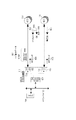
図4は従来のライト(W)コマンド&ステータス及び異常時のリカバリーシーケンスを示す図である。 FIG. 4 is a diagram showing a conventional write (W) command & status and a recovery sequence at the time of abnormality.
図4(a)は、画像処理装置がミラー状態であることを示す図である。SATAホスト制御部111は、上位からの書込み要求に対してライト(W)コマンド401をSATAブリッジ制御部112に送信する。そして、Wコマンド401を受信したSATAブリッジ制御部112はコマンド解釈を実行する。そしてSATAブリッジ制御部112は、HDD113及びHDD114に対してWコマンド401と同じ内容のWコマンド402、403を送信し、タイムのカウントを開始する。
FIG. 4A is a diagram showing that the image processing device is in the mirror state. The SATA
Wコマンドを受け付けたHDD113及びHDD114は、SATAブリッジ制御部112に応答(後述のDMAactパケット)を返す。そして、ここでは詳細な説明は省略するが、SATA規格のフロー制御に基づいてSATAホスト制御部111は、1つのライト(W)データ404を一定のデータパケット単位410で分割してSATAブリッジ制御部112に送信する。
The
ここで、SATA規格でのデータ単位について説明する。SATA規格で送受信される1個のコマンドに対するデータ転送の最大サイズはWデータ404に示すように32MBで、伝送路で送受信される1回のデータパケット単位410は8KBである。
Here, the data unit in the SATA standard will be described. The maximum size of data transfer for one command transmitted / received according to the SATA standard is 32 MB as shown in
SATAブリッジ制御部112は、SATA−IP203、204、205の内部にバッファを持つ。本実施例では、各バッファサイズの例としてデータパケット単位8KB×2個分の16KBを保持可能な容量としている。
The SATA
一般的に1個のコマンド処理でのデータサイズを大きくすることで処理効率は向上する。本例では各バッファ411、412、413を16KBとしているが、本サイズは引き出したいパフォーマンスによって決められるべき値であり、この値に限定するものではない。
Generally, processing efficiency is improved by increasing the data size in one command processing. In this example, each
図4(a)の説明に戻る。SATAホスト制御部111からSATAブリッジ制御部112に送信されたWデータ(Wデータ404の一部のデータ)が、バッファ411に保持される。バッファ411に保持されたWデータを、SATAブリッジ制御部112が、バッファ412,413に保持させる。そして、SATAブリッジ制御部112は、バッファ412、413に保持されたデータをWデータ405およびWデータ406としてHDD113及び114に逐次送信する。一方、バッファ411は、前のWデータを消去して次のWデータを受信して保持する。なお、以下では、前のWデータの消去については説明を省く。これは、バッファ412と413においても同様である。
Returning to the description of FIG. 4 (a). The W data (a part of the data of the W data 404) transmitted from the SATA
少なくとも一方のHDDにおいてWデータの書き込みが終わると、SATAブリッジ制御部112は、バッファ411から書き込みが完了したHDDに対応するバッファに次のWデータ(Wデータ404の一部)を保持させる。例えば、HDD113への書き込みが先に終わり、HDD114への書き込みが後に終わる場合には、バッファ412に次のWデータが保持された後にバッファ413に次のWデータが保持される。同時に書き込みが終わった場合には、バッファ412とバッファ413に同時に次のWデータが保持される。なお、バッファは、前述したように、前のWデータを消去して次のWデータを保持する。
When the writing of the W data is completed in at least one HDD, the SATA
そして、SATAホスト制御部からSATAブリッジ制御部112に送信されたWデータ411の全てが、SATAブリッジ制御部112を介してHDD113およびHDD114に記憶されるまで上述の送信が繰り返される。
Then, the above transmission is repeated until all of the
ここで、予め設定されたタイムアウト時間内にWデータ404の全ての送信がHDD113、HDD114の両方に正常に転送完了すると、SATAブリッジ制御部112は両デバイスのそれぞれからOK(正常)ステータス407、408を受信する。
Here, when all the transmissions of the
このような場合にSATAブリッジ制御部112は、SATAホスト制御部111に対して書込み処理正常終了としてOKステータス409を送信する。SATAブリッジ制御部112からOKステータスを受信したSATAホスト制御部111はWコマンド401の一連の処理を終了する。
In such a case, the SATA
このように、HDD113及び114は双方のデータ保持状態が同一レベルであり整合性が取れている状態を、ミラーリングの正常状態としてミラーリング状態と定義する。
In this way, the states in which the data holding states of both
なお、本実施例ではHDD113をマスターストレージ、HDD114をスレーブストレージとして説明する。ここでは図示しないが、リード(R)コマンド発行時はマスターからのみ読み出し処理が実行される。
In this embodiment, the
図4(b)においてSATAブリッジ制御部112が、書き込みに失敗した旨のステータス(NGステータス)を一方のHDDから受け付けた状況の一例を説明している。
FIG. 4B illustrates an example of a situation in which the SATA
具体的には、HDD114のスレーブ側が書き込み処理途中に何らかの原因で失敗した場合を示す。
Specifically, it shows a case where the slave side of the
このとき、SATAブリッジ制御部112がNG(失敗)ステータス408を受信し、BCPU310はスレーブ側のHDD114に対して停止処理を実行する。停止処理を実行すると、SATAブリッジ制御部112は、SATAホスト制御部111から受け付けたWデータ404の一部をバッファ413に送信しなくなり、バッファ412にのみ送信する。
At this time, the SATA
つまり、BCPU310は、正常なHDD113が接続されたマスター側に対して書き込み処理を継続し、書き込みに失敗したHDD114が接続されたスレーブ側のSATA‐IP205を初期化して現行の書込み処理を実行しなくなる。このSATAIP205の初期化処理によって、SATAブリッジ制御部112は、SATAブリッジ制御部112に接続されたストレージがHDD113のみであると認識する。なお、初期化処理は実施せず、ただ無視することができるのであればそれでもよい。
That is, the
タイムアウト時間内にマスター側の書き込み処理が完了すると、SATAブリッジ制御部112はマスター側のHDD113からOKステータス407を受信する。これによりSATAブリッジ制御部112は、本書き込み処理は正常に完了したとして上位SATAホスト制御部111にOKステータス409を送信する。OKステータス409を受信したSATAホスト制御部111は本書き込み処理を終了し、次のコマンドが送信可能となる。
When the writing process on the master side is completed within the timeout time, the SATA
一方、SATAブリッジ制御部112のBCPU310は、未使用処理時に前回書き込み処理時の開始アドレス及びデータサイズをSRAM313に記録した情報に基づき、失敗した側のリカバリ処理をバックグラウンドで開始する。
On the other hand, the
図4(c)を用いて図4(b)の後のリカバリ処理について説明する。SATAブリッジ制御部112は、書き込み処理に失敗したHDD114の初期化処理を行い、前回書き込み処理に成功したHDD113から記録した開始アドレス及びデータサイズのデータの読み出し処理(R)414を開始する。
The recovery process after FIG. 4 (b) will be described with reference to FIG. 4 (c). The SATA
読み出したデータを、書き込み処理に失敗した側HDD114に対して同一アドレスから逐次書き込み処理(W)415を実行する。
The read data is sequentially written from the same address to the
リカバリ処理中に書き込みエラーが生じた場合、画像形成装置は、ここでは図示しないが予め設定された回数のリカバリ処理を繰り返す。予め設定された回数のリカバリ処理の中でリカバリ処理に成功すれば、画像形成装置は、ミラー状態に遷移する。 If a write error occurs during the recovery process, the image forming apparatus repeats the recovery process a preset number of times (not shown here). If the recovery process is successful in the preset number of recovery processes, the image forming apparatus transitions to the mirror state.
予め設定された回数のリカバリ処理の全てで失敗した場合には、HDD114はシステム的に使用不能になりHDD交換通知がなされ、片側HDD113のみ(デグレード状態)で装置の運用が継続される。
If all of the recovery processes set in advance fail, the
この時、HDD交換通知は割り込み信号318によりSATAホスト制御部111に通知される。ここでは省略するが、SATAホスト制御部111は、SATAブリッジ制御部112の内部状態を取得するGetBridgeInfoコマンド1008を有し、それによってどちらのHDDを交換すべきかを判断することができる。
At this time, the HDD replacement notification is notified to the SATA
なお、SRAM313に記録した情報は、BCPU310によって利用後消去される。また、ミラーリング状態(例えば、ミラー状態、デグレード状態)は、SATAブリッジ制御部112内のSRAM313やレジスタB314などに記録されている。
The information recorded in the
図5は、課題が生じる構成としてWコマンド501に対して無応答のHDDが生じる構成について説明する。
FIG. 5 describes a configuration in which an HDD that does not respond to the
図5は、SATAホスト制御部111がSATAブリッジ制御部112にWコマンド501とWデータ503の一部のデータ(データパケット単位410で送付されたデータ)を送信する。SATAブリッジ制御部112は、一部のデータをバッファ411に保持し、SATAブリッジ制御部112は、保持した一部のデータをバッファ412および413に保持する。
In FIG. 5, the SATA
そしてSATAブリッジ制御部112は、HDD113およびHDD114にWコマンドを送信し、WコマンドをHDD113およびHDD114に送信することを起点にタイマー(経過時間の閾値)を設定し、時間のカウントを開始する。
Then, the SATA
図5においてHDD113は、Wコマンドに対応してデータ転送開始割り込みを示すDMAactパケット502をSATAブリッジ制御部112に返す。DMAactパケット502を受け付けたSATAブリッジ制御部112は、バッファ411に保持した一部のデータをHDD113に送信する。HDD113が受信した一部のデータを書き込むと、次の一部のデータをバッファ411から受信するためにDMAactパケット502をSATAブリッジ制御部112に出力する。
In FIG. 5, the
なお、DMAactパケット502は、SATAブリッジ制御部112に対してバッファ412に保持された分割されたデータを送信させるためにHDD113が送付するコマンドである。
The
一方、図5においてHDD114は、設定されたタイマーの時間内にWコマンドに応答しない。例えば、HDDの寿命が近い場合や寿命が尽きている場合などにこのような無応答が生じる。このような状態では、HDD114は、DMAactパケット502をSATAブリッジ制御部112に返さない。
On the other hand, in FIG. 5, the
そのため、SATAブリッジ制御部112のバッファ412が2回目にフル状態になり、HDD113に2回目の分割データの書き込みを終えた時点で、無応答側のバッファ413には1回目の分割データが保持されているという状況が発生する。このような状況が発生すると、バッファ413に2回目の分割データを保持させていないため、バッファ412に3回目の分割データを保持させることが出来ない。言い換えると、HDD114に1回目のデータを記憶させていないことで、HDD113に2回目の分割データまで記憶させることはできるが、3回目以降の分割データを記憶させることはできない。
Therefore, when the
このような状況が発生するとバッファ412側を制御しているSATAーIP204は、HDD113に対してHoldパケット506を発行する。それを受けたHDD113側はHoldA507を返し、待機状態になる。
When such a situation occurs, the SATA-IP204 controlling the
一方、HDD114側は無応答のままであるため、タイマーの時間内にSATAブリッジ制御部112は両方のHDDからのOKステータスを受信することなくタイムアウトとなる(設定した経過時間の閾値を超える)。
On the other hand, since the
SATAブリッジ制御部112は、双方のHDD113、114にWコマンドを発行したにも係わらずタイムアウトし、書き込み処理が完了しなかったため、SATAホスト制御部111に対してNG(失敗)ステータス409を送信する。
The SATA
NGステータスを受信したSATAホスト制御部111は、再書き込み処理(同一Wコマンド501を再度発行する)をSATAブリッジ制御部112に指示する。
Upon receiving the NG status, the SATA
前述したようにHDDが無応答になる現象は、ストレージデバイスの経年変化が進むことによって生じる。そして、無応答になったHDDは、電源OFF→ONすることにより一時的に回復する可能性があるが、すぐに無応答になる現象が生じてしまう。 As described above, the phenomenon that the HDD becomes unresponsive occurs due to the aging of the storage device. Then, the HDD that has become unresponsive may be temporarily recovered by turning the power off and then on, but a phenomenon that the HDD becomes unresponsive immediately occurs.
つまり、SATAホスト制御部111が指示した再書き込み処理も失敗する可能性が高い。その結果、使用可能なHDDがあっても、SATAホスト制御部111は、すべてのHDDが使用不能であると把握してしまい、システム的な破綻に至る可能性がある。さらに、SATAホスト制御部111は、SATAブリッジ制御部112からNGのステータスを取得してもどのHDDが無応答状態のであるかを判定することが出来ない。
That is, there is a high possibility that the rewrite process instructed by the SATA
図6は、本実施例における無応答ストレージ発生時の停止処理を説明する構成である。本実施例では、一方のHDDが無応答状態に陥った際に一方のHDDへのデータの送信を停止し、他方へのHDDにデータの送信を継続する。そして、他方のHDDが書き込み処理に成功すれば、上位回路(SATAホスト制御部111)に書き込み処理に成功した旨の通知を行う。以下で詳細を説明する。なお、図5の説明と同様の部分については説明を省略する。 FIG. 6 is a configuration for explaining the stop processing when the non-response storage occurs in this embodiment. In this embodiment, when one HDD falls into a non-response state, the transmission of data to one HDD is stopped, and the transmission of data to the other HDD is continued. Then, if the other HDD succeeds in the writing process, the host circuit (SATA host control unit 111) is notified that the writing process is successful. Details will be described below. The same parts as those in FIG. 5 will be omitted.
図6の場合もSATAブリッジ制御部112は、SATAホスト制御部111からWコマンドを受け付け、1回目の分割データを受け付けてバッファ411に保持してからバッファ412とバッファ413に保持する。SATAブリッジ制御部112は、HDD113およびHDD114にWコマンド402及びWコマンド403を送信し、Wコマンドの送信を起点として第1タイマー(時間経過の第1閾値)を設定し、第1タイマーに対する時間のカウントを開始する。
Also in the case of FIG. 6, the SATA
SATAブリッジ制御部112は、HDD113およびHDD114の少なくとも一方からWコマンドへの応答(例えば、DMAactパケット502(データ転送開始割り込み))を受け付ける。応答を受信したBCPU310はHDD113側がデータ転送開始したことをSRAM313又はレジスタB314などに記憶する。そして、SATAブリッジ制御部112は、応答(データ転送開始割り込み)を起点として第2タイマー(経過時間の第2閾値)を設定し、第2タイマーに対する時間のカウントを開始する。この第2閾値は、第1閾値値よりも短い値となる。
The SATA
SATAブリッジ制御部112は、応答(データ転送開始割り込み)を受け付けない状態で第2タイマーがタイムアップした場合(経過時間が第2閾値を超えた場合)には、HDD114側の停止処理を行う。停止処理およびその後のリカバリ処理は、図4(b)、図4(c)と同様であるため説明を省略する。
When the second timer times up (when the elapsed time exceeds the second threshold value) in a state where the response (data transfer start interrupt) is not received, the SATA
SATAブリッジ制御部112は、第2タイマーの時間内にHDD114から応答(データ転送開始割り込み)を受け付けた場合には、HDD114側への書込み処理を継続する。
When the SATA
なお、SATAブリッジ制御部112から各デバイスに対してコマンドが発行できるのは、各HDDがレディ状態(ビジーではない)であることを意味する。一旦コマンドを発行すると後はHDD側の応答を待つしかすべがない。
The fact that the SATA
第2タイマーを設定することによって、Wコマンド送付後の無応答などの故障発生時に正常なデバイスが異常なデバイスに引きずられてコマンド処理失敗となることを回避することができる。 By setting the second timer, it is possible to prevent a normal device from being dragged by an abnormal device and causing a command processing failure when a failure such as no response occurs after sending a W command.
いずれかのHDDへのデータ転送が開始されるとそれを通知する割り込み信号を設ける。その割り込み信号を割り込み制御部316から受信したBCPU310は、受信したSATA−IP側を記憶しておき、第2タイマーを設定する。
An interrupt signal is provided to notify when data transfer to any HDD is started. The
なお、ここではデータ転送開始をSATA−IPからの割り込み信号で検知する例を示しているが、この方法に限定するものではない。他の例としてテータ転送回数のカウンタ値の変化から検知するなどであっても構わない。 Although an example in which the start of data transfer is detected by an interrupt signal from SATA-IP is shown here, the method is not limited to this method. As another example, it may be detected from a change in the counter value of the number of times the data is transferred.
次に図7を用いて図6で説明した本実施例の構成を実現するための書込み処理フローの一例を説明する。本実施例のフローチャートは、BCPU310によって実行され、HDDへのアクセスが生じると開始する。
Next, an example of a write processing flow for realizing the configuration of the present embodiment described with reference to FIG. 6 will be described with reference to FIG. 7. The flowchart of this embodiment is executed by the
ステップS601において、SATAブリッジ制御部112を制御しているBCPU310は、ステップS601においてSATAホスト制御部111からWコマンドを受信する。
In step S601, the
ステップS602においてBCPU310は、受信したコマンドの内容を解釈し、同一内容のWコマンドを接続されているHDD113及び114に送信する。そして、ステップS602を終えるとステップS603において、第1タイマー(経過時間の第1閾値)をタイマー回路に設定し、本コマンド処理全体に対する制限時間のカウントを開始する。なお、第1タイマーの設定およびカウント開始は、WコマンドをHDD113およびHDD114に送信することが起点であればよいためステップS602とS603は同時でも逆でもよい。なお、タイマー回路は、SATAブリッジ制御部112に含まれる。
In step S602, the
ステップS604においてBCPU310は、HDDの一方から応答(データ転送開始割り込み)を待つ。一方のHDDから応答を受け付けると、HCPU301は、応答を返してきたHDDへのデータ転送を開始する。一方のHDDへのデータ転送を開始したらステップS605に遷移する。ステップS605において第2タイマー(経過時間の第2閾値)をタイマー回路に設定し、まだデータ転送開始していないデバイスに対する制限時間のカウントを開始する。なお、第2タイマーの設定およびカウント開始は、応答をHDD113またはHDD114から受信することが起点である。
In step S604, the
ここで、第1タイマー及び第2タイマーを設定するタイマー回路はひとつ以上あればよい。ひとつの場合には第1タイマーの残り時間を記録しておき第2タイマーを設定し、第2タイマーの経過後、再び第1タイマーの残りの時間を設定すればよい。タイマー回路の使い方は特に限定しない。 Here, it is sufficient that there is one or more timer circuits for setting the first timer and the second timer. In one case, the remaining time of the first timer may be recorded, the second timer may be set, and after the lapse of the second timer, the remaining time of the first timer may be set again. The usage of the timer circuit is not particularly limited.
次に、ステップS606においてBCPU310は、他方のHDD側がデータ転送を開始したか否かの判定を実施する。
Next, in step S606, the
ステップS606においてBCPU310は、HDDの他方から応答(データ転送開始割り込み)を受け付けると、BCPU310は、応答を返してきたHDDへのデータ転送を開始する。他方のHDDへのデータ転送を開始したらステップS608に遷移する。
When the
ステップS608で第2タイマーを解除し、ステップS609において両HDDに対する図4で説明した通常処理を実行し、ステップS612に遷移する。なお、第2タイマーの解除とは、例えば、第2タイマーの設定を解除し、且つ、第2タイマーに対する経過時間のカウントを停止することである。 The second timer is canceled in step S608, the normal processing described with reference to FIG. 4 is executed for both HDDs in step S609, and the process proceeds to step S612. The cancellation of the second timer means, for example, canceling the setting of the second timer and stopping the counting of the elapsed time with respect to the second timer.
ステップS606の説明に戻る。ステップS606において、他方のHDDから応答を受け付けていない場合には、データ転送を開始していないためステップS607に遷移する。ステップS607において第2タイマーがタイムアウトしているか否かの判定を行う。言い換えると、経過時間が第2閾値を超えたか否かの判定を行う。 Returning to the description of step S606. If the response is not received from the other HDD in step S606, the data transfer is not started, so the process proceeds to step S607. In step S607, it is determined whether or not the second timer has timed out. In other words, it is determined whether or not the elapsed time exceeds the second threshold value.
ステップS607において第2タイマーがタイムアウトしていない場合には、ステップS606に戻る。 If the second timer has not timed out in step S607, the process returns to step S606.
ステップS607において第2タイマーがタイムアウト時間を過ぎているか場合には、ステップS610に遷移する。ステップS610においてBCPU310は、Wコマンドに対して無応答である(データの転送を開始できない)HDD114に対して停止処理を実行する。具体的には、HDD114側のバッファ413へのデータ転送を停止する停止処理を実行する。ステップS610を終えるとステップS611に遷移する。ステップS611において、ステップS604でデータ転送を開始したHDD113のデータ転送を継続して行い、ステップS612に遷移する。
If the second timer has passed the timeout time in step S607, the process proceeds to step S610. In step S610, the
ステップS612において、BCPU310は、HDD113およびHDD114の両方のHDDの書き込み処理のステータスが所定のステータスであるか否かの判定を行う。所定のステータスは、2通りある。ステップS611からステップS612に遷移した場合、所定のステータスは、HDD113の書き込み処理のステータスが正常に完了、または、エラーを示すステータスであることである。
In step S612, the
ステップS609からステップS612に遷移した場合、少なくとも1つのHDDの書き込み処理が正常に完了したことを示すステータスであること、または、すべてのHDDの書き込み処理がエラーになったことを示すステータスであることである。なお、少なくとも1つのHDDの書き込み処理が正常に完了したことを示すステータスであるとは、例えば、HDD113は正常なステータスを示し、HDD114は、エラーもしくは書き込み処理実行中である場合である。
When transitioning from step S609 to step S612, the status indicates that the writing process of at least one HDD has been completed normally, or the status indicates that the writing process of all HDDs has become an error. Is. The status indicating that the writing process of at least one HDD has been completed normally is, for example, the case where the
ステップS612において、所定のステータスではない場合には、ステップS613に遷移する。ステップS613において、第1タイマーがタイムアウトしていない場合には、ステップS609またはステップS611に戻る。一方、ステップS613において、第1タイマーがタイムアウトした場合(経過時間が第1閾値を超えた場合)には、ステップS616に遷移する。具体的には、ステップS611を介した場合、HDD113の書き込み処理が第1タイマーの時間内で終了しない場合である。ステップS609を介した場合、HDD113及びHDD114の一方がエラーで他方の書き込み処理が第1タイムアウト時間内に終了していない場合、または、両方のHDDの書き込み処理が第1タイムアウト時間内に終了していない場合である。
In step S612, if the status is not the predetermined status, the process proceeds to step S613. If the first timer has not timed out in step S613, the process returns to step S609 or step S611. On the other hand, in step S613, when the first timer times out (when the elapsed time exceeds the first threshold value), the process proceeds to step S616. Specifically, in the case of going through step S611, the writing process of the
これらの場合、ステップS616においてBCPU310は、書き込み処理がエラー状態であると判断する。そして、SATAブリッジ制御部112は、SATAホスト制御部111にエラーである旨のステータス(失敗通知)を送信する。ステップS616を終えるとフローが終了する。
In these cases, in step S616, the
ステップS612の説明に戻る。ステップS612において、所定のステータスである場合には、ステップS614に移行する。ステップS614においてBCPU310は、第1タイマーを解除する。なお、第1タイマーを解除するとは、例えば、第1タイマーの設定を解除し、第1タイマーに対する経過時間のカウントを停止することである。ステップS614を終えるとステップS615に移行する。
Returning to the description of step S612. In step S612, if the status is predetermined, the process proceeds to step S614. In step S614, the
次のステップS615において、HDD113およびHDD114の少なくとも一方の書き込み処理の結果が成功しているか否かを判定する。ステップS615がNoの場合、すなわち両HDDともに失敗の場合にはステップS616に進む。ステップS616は既に説明済みなので省略する。
In the next step S615, it is determined whether or not the result of the writing process of at least one of the
ステップS615がYesの場合には、すなわちHDD113およびHDD114の少なくとも一方の書き込み処理の結果が成功している場合には、ステップS617に遷移する。ステップS617において要求元であるSATAホスト制御部111に対してWコマンドに基づく書き込み処理が正常に完了した旨のステータス(完了通知)を送信する。これにより、SATAブリッジ制御部112とSATAホスト制御部111間の処理が終了する。なお、S617の後にS614を行ってもよい。
If step S615 is Yes, that is, if the result of the writing process of at least one of
ステップS618においてBCPU310は、リカバリ処理の有無を判定する。ステップS618においてリカバリ処理がない場合、すなわち両HDDともに成功の場合には、フローを終了し、次のコマンドを受付可能な状態に戻る。
In step S618, the
ステップS618においてBCPU310が、リカバリ処理がある状態と判断するとステップS619に遷移する。なおリカバリ処理が有る状態とは、例えば、停止処理をしたHDDが有る場合、または、エラーステータスのHDDが有る場合である。
If the
ステップS619においてBCPU310は、NG側のリカバリ(修復)処理を開始する。リカバリ処理は、既に図4(c)で説明した内容であるので省略する。リカバリ処理は必要に応じて予め設定されたリトライ回数分繰り返される。
In step S619, the
ステップS620においてBCPU310は、リカバリ処理のn−1回目までが成功したか否かの判定を行う。ステップS620においてn−1回目までのどこかで成功(Yes)すれば、その後次のコマンド受付状態に戻る。
In step S620, the
ステップS620において、リカバリ処理をn−1回目まで行っても成功しなかった場合には、ステップS622に進む。ステップS622においてBCPU310は、リカバリ処理に電源OFF/ONを実行するかどうかの判定を行う。ここで、電源OFF/ON条件は予め設定されているものとする。
If the recovery process is not successful even if the recovery process is performed up to the n-1th time in step S620, the process proceeds to step S622. In step S622, the
ステップS622がYesの場合には、BCPU310は電源IF部315を介して電源制御部209に所望のデバイス側の電源をOFF→ON制御を行う。例えば、図5(b)で説明した無応答でのリカバリ処理時に電源OFF/ON実行が有効であれば、失敗しているHDD114の電源をOFF→ONして修復作業を試みる。そして、ステップS624の判定において修復成功(Yes)であれば次のコマンド受付状態に戻る。ステップS622がNo又はステップS624が失敗(No)した場合にはステップS625に進む。なお、ステップS622およびステップS623は、なくてもよい。
When step S622 is Yes, the
ステップS625においてBCPU310は、リカバリ側のデバイスをシステム的に未使用にするためにデグレード状態として運用を継続する。さらにNG側デバイスを特定して交換作業の警告を、例えばパネルIF部115を介してパネル装置116に表示する。
In step S625, the
このような構成によれば、書き込みコマンドに対して所定時間内に応答がないストレージがあったとしてもホストコントローラにすべてのストレージがエラー状態であると誤認識させないことが可能である。 According to such a configuration, even if there is a storage that does not respond to the write command within a predetermined time, it is possible to prevent the host controller from erroneously recognizing that all the storages are in an error state.
(実施例2)
図8では、実施例2における無応答ストレージ発生時の停止処理を説明する構成図を説明する。
(Example 2)
FIG. 8 describes a configuration diagram for explaining the stop processing when the non-response storage occurs in the second embodiment.
図8は、SATAブリッジ制御部112を搭載せず、SATAホスト制御部111に2個のHDD113、114を接続してミラーリング処理を実施する場合の例である。図8においてSATAホスト制御部111は、SATA−IP704とSATA−IP705を有し、これらは、図3のSATA−IP204とSATA−IP205と同等の機能を有する。そのため、バッファ702及び703は、Host1及び2に対するデータ送受信バッファであり、図4で説明したバッファ412、413に該当するものと同等の機能となる。
FIG. 8 shows an example in which the SATA
なお、図8の書込み処理については図5の処理と同じであるため同等の機能を有する構成には図4、5と同じ番号を用いて説明する。 Since the writing process of FIG. 8 is the same as the processing of FIG. 5, a configuration having the same function will be described using the same numbers as those of FIGS. 4 and 5.
バッファ702及び703は、Host1及び2に対するデータ送受信バッファであり、図4で説明したバッファ412、413に該当するものと同等の機能となる。バッファ702はSATA−IP(Host1)204に含まれ、バッファ703は、SATA−IP(Host2)205に含まれる。
The
SATAホスト制御部111は、CPU101からWコマンドを受け付ける。SATAホスト制御部111は、Wコマンドを受け付けると、DMAC701によってメインバス上に接続されるDRAM104から書き込みを行うデータを取得する。DMAC701は、取得したデータを各バッファ702、703に実施例1で説明した構成と同様に分割して保持させる。
The SATA
また、DMAC701はひとつのチャンネルしか持たないのでWコマンド501に対するWデータ503を各バッファに保持させる際には、各バッファに分割データを送信する必要がある。従って、HDD114がWコマンドに対して無応答状態に陥るとバッファ703が2回目の分割データから送信できなくなる。
Further, since the DMAC701 has only one channel, when the
そこで、本実施例においても、一方のHDDが無応答状態に陥った際に一方のHDDへのデータの送信を停止し、他方へのHDDにデータの送信を継続する。そして他方のHDDが書き込み処理に成功すれば、上位回路(CPU101)に書き込み処理に成功した旨の通知を行う。図8を用いて詳細を説明する。 Therefore, also in this embodiment, when one HDD falls into a non-response state, the transmission of data to one HDD is stopped, and the transmission of data to the other HDD is continued. Then, if the other HDD succeeds in the writing process, the host circuit (CPU101) is notified that the writing process is successful. Details will be described with reference to FIG.
まず上位のCPU101からSATAホスト制御部111がWコマンドを受け付ける。SATAホスト制御部111がHDD113およびHDD114にWコマンド402及びWコマンド403を送信し、Wコマンドの送信を起点として第1タイマーを設定し、第1タイマーに対するタイムカウントを開始する。
First, the SATA
SATAブリッジ制御部112は、HDD113およびHDD114の一方からWコマンドへの応答(例えば、DMAactパケット502)を受け付ける。応答を受信したHCPU301はHDD113側がデータ転送開始したことをSRAM304又はレジスタH306などに記憶する。そして、SATAホスト制御部111は、応答(データ転送開始割り込み)を起点として第2タイマーを設定し、第2タイマーのタイムカウントを開始する。この第2タイマー(経過時間の第2閾値)は、第1タイマー(経過時間の第1閾値)よりも短い値となる。
The SATA
SATAホスト制御部111は、第2タイマーがタイムアウトしてもHDD114から応答(データ転送開始割り込み)を受け付けなかった場合には、HDD114側に対して停止処理を行う。そして、第1タイマーがタイムアウトする前に、HDD113から書き込み処理に成功した旨の通知を受け付けると、CPU101に書き込み処理に成功した旨の通知を送信する。なお、停止処理およびその後のリカバリ処理は説明を省略する。
If the SATA
SATAホスト制御部111は、第2タイマーがタイムアウトする前にHDD114から応答(データ転送開始割り込み)を受け付けた場合には、HDD114側への書込み処理を継続する。そして、第1タイマーがタイムアウトする前に、HDD113とHDD114の少なくとも1つから書き込み処理に成功した旨の通知を受け付けると、CPU101に書き込み処理に成功した旨の通知を送信する。
If the SATA
なお、SATAホスト制御部111から各デバイスに対してコマンドが発行できるのは、各HDDがレディ状態(ビジーではない)であることを意味する。一旦コマンドを発行すると後はHDD側の応答を待つしかすべがない。
The fact that the SATA
なお、実施例1と同様に、ここではデータ転送開始をSATA−IPからの割り込み信号で検知する例を示しているが、この方法に限定するものではない。他の例としてテータ転送回数のカウンタ値の変化から検知するなどであっても構わない。 As in the case of the first embodiment, an example in which the start of data transfer is detected by an interrupt signal from SATA-IP is shown here, but the method is not limited to this method. As another example, it may be detected from a change in the counter value of the number of times the data is transferred.
このような構成においても、書き込みコマンドに対して所定時間内に応答がないストレージがあったとしてもホストコントローラ(ここではCPU101)にすべてのストレージがエラー状態であると誤認識させないことが可能である。 Even in such a configuration, it is possible to prevent the host controller (here, CPU101) from erroneously recognizing that all the storages are in an error state even if there is a storage that does not respond to the write command within a predetermined time. ..
(第2実施形態)
図面9および図10を参照して本実施形態の実施例を詳しく説明する。第1実施形態と同様の構成については同じ番号を付して説明を省略する。
(Second Embodiment)
Examples of this embodiment will be described in detail with reference to FIGS. 9 and 10. The same configuration as that of the first embodiment will be assigned the same number and description thereof will be omitted.
(実施例3)
図9では、無応答ストレージの発生によって生じる課題に対応するための本実施例の制御構成を説明する。
(Example 3)
FIG. 9 describes a control configuration of the present embodiment for dealing with a problem caused by the occurrence of non-responsive storage.
図9のDMAC801は、独立に処理可能なチャンネルを2個搭載し、DMAC801のCH0はバッファ702と、CH1はバッファ703と接続されている。
The DMAC801 of FIG. 9 is equipped with two channels that can be processed independently, and CH0 of the DMAC801 is connected to the
本構成においても、図に示すようにHDD114がWコマンド805を送信した後に無応答809に陥っても、すべてのHDDがエラー状態であると誤認識させないことが可能である。
Also in this configuration, as shown in the figure, even if the
SATAホスト制御部111は、CPU101からWコマンドを受け付けると、HDD113およびHDD114にWコマンドを出力する。そして、SATA‐IP704がHDD113から応答(DMAact806)を受け付けると、HCPU301は、応答を起点として第3タイマーを設定し、制限時間のカウントを開始する。
When the SATA
図9の構成においては、HDD113の書込み処理とHDD114の書き込み処理は、独立して実行可能である。そのため、SATAホスト制御部111は、HDD114の書き込み処理の状況に係わらず、HDD113側からのDMAact806を毎回の起点としたデータパケット単位での転送を継続して実行可能である。
In the configuration of FIG. 9, the writing process of the
そのため、HDD114側が無応答状態となってもHDD113側は書き込み処理に成功することが出来る。具体的には、SATAホスト制御部111は、HDD113側において、第3タイマーがタイムアウトする前に、書き込み処理に成功した旨のステータス808を受信することが出来る。一方、無応答状態のHDD114側は、第2タイマーがタイムアウトしても書き込み処理を完了させることができない。その停止処理が実行され、HCPU301が、HDD114側がエラーステータスであると判断する。
Therefore, even if the
このような状況において、HCPU301は、CPU101に対して書込み処理成功として書込み完了割り込み信号を発行する。一方、停止処理されたHDD114の以後のバックグラウンドでのリカバリ処理は図4(c)で説明済みなので説明を省略する。
In such a situation, the
図10を用いて図9で説明した本実施例の構成を実現するための書込み処理フローの一例を説明する。図10は、図9で説明した独立した2チャンネルを有するDMACを搭載したミラーリング構成での書込み処理に対する処理フローを示す図である。図7と同様の構成については同様の番号を付して説明を省略する。図10のフローチャートは、HCPU301によって実行される。
An example of a write processing flow for realizing the configuration of the present embodiment described with reference to FIG. 9 will be described with reference to FIG. FIG. 10 is a diagram showing a processing flow for a writing process in a mirroring configuration equipped with a DMAC having two independent channels described with reference to FIG. The same configuration as in FIG. 7 will be assigned the same number and the description thereof will be omitted. The flowchart of FIG. 10 is executed by the
HCPU301は、ステップS901において上位アプリケーション(CPU101)からWコマンドを受信する。ステップS902においてHCPU301は、受信したコマンドの内容を解釈し、同一内容のWコマンドを接続されているHDD113及び114に送信する。
The
ステップS903においてHCPU301は、HDD113またはHDD114の少なくとも一方の応答(データ転送開始割り込み)を待つ。少なくとも一方のHDDから応答を受け付けると、HCPU301は、応答を返してきたHDDへのデータ転送を開始する。少なくとも一方のHDDへのデータ転送を開始したらステップS904に遷移する。
In step S903, the
ステップS904において第3タイマー(時間経過の第3閾値)をタイマー回路に設定し、本コマンド処理全体に対する制限時間のカウントを開始する。 In step S904, a third timer (third threshold value for the passage of time) is set in the timer circuit, and counting of the time limit for the entire command processing is started.
ステップS905において第3タイマーを設定後もデータ転送およびHDDの書き込み処理は継続される。 Even after the third timer is set in step S905, the data transfer and HDD write processing are continued.
ステップS906において、HCPU301は、HDD113およびHDD114の両方のHDDの書き込み処理のステータスが所定のステータスであるか否かの判定を行う。
In step S906, the
所定のステータスとは、少なくとも1つのHDDの書き込み処理が正常に完了したことを示すステータスであること、すべてのHDDの書き込み処理がエラーになったことを示すステータスであること、のいずれかのステータスとなる。なお、少なくとも1つのHDDの書き込み処理が正常に完了したことを示すステータスであるとは、例えば、HDD113は正常なステータスを示し、HDD114は、エラーもしくは書き込み処理実行中である場合である。
The predetermined status is either a status indicating that the writing process of at least one HDD has been completed normally, or a status indicating that the writing process of all HDDs has become an error. It becomes. The status indicating that the writing process of at least one HDD has been completed normally is, for example, the case where the
ステップS906において、所定のステータスではない場合には、ステップS907に遷移する。 In step S906, if the status is not the predetermined status, the process proceeds to step S907.
ステップS907においてHCPU301は、第3タイマーがタイムアウトしたかどうかの判定を行う。第3タイマーがタイムアウトしていない場合には、ステップS905に戻り、処理を継続する。ステップS907において、第3タイマーがタイムアウトした場合には、ステップS910に遷移する。ステップS910において、HCPU301は、CPU101にエラーステータスを送信する。
In step S907, the
ステップS906の説明に戻る。ステップS906において、所定のステータスではある場合には、ステップS909に遷移する。 Returning to the description of step S906. In step S906, if the status is predetermined, the process proceeds to step S909.
ステップS909においてHCPU301は、HDD113およびHDD114の書き込み処理の結果(ステータス)を確認する。HDD113およびHDD114の両方のステータスが、書き込み処理の失敗を示している場合には、ステップS910に遷移する。
In step S909, the
ステップS909において、すべてのHDDのステータスが、書き込み処理の成功を示す場合、または少なくとも1つのHDDのステータスが書き込み処理の成功を示す場合には、ステップS911に遷移する。 In step S909, if the statuses of all HDDs indicate the success of the write process, or if the status of at least one HDD indicates the success of the write process, the process proceeds to step S911.
ステップS911において、HCPU301は、要求元であるCPU101に対してWコマンド処理正常としてステータスを送信し、CPU101とSATAホスト制御部111の間の処理は終了する。
In step S911, the
ステップS912においてHCPU301は、第3タイマーがタイムアウトしたかどうかの判定を行う。ステップS907において、第3タイマーがタイムアウトした場合には、ステップS910に遷移する。ここでは詳細な説明は省略するが、この場合ステップS910においてHCPU301は、CPU101とのやり取りは完了しているため、その他所定のエラー処理を実行する。第3タイマーがタイムアウトしていない場合には、ステップS913に進む。ステップS913においてHCPU301は、もう一方のHDDが処理継続中かどうかの判定を行う。ステップS913の判定結果がYesの場合には、ステップS902に戻り、S912及びS913の間を繰り返す。ステップS913の判定結果がNoの場合には、ステップS914に進む。ステップS914においてHCPU301は、第3タイマーの設定を解除し、ステップS618に遷移する。
In step S912, the
ステップS618〜S625については、説明を省略する。なお、本フローチャートでは、図7のS621〜S623を省略している。 The description of steps S618 to S625 will be omitted. In this flowchart, S621 to S623 of FIG. 7 are omitted.
このような構成においても、書き込みコマンドに対して所定時間内に応答がないストレージがあったとしてもホストコントローラにすべてのストレージがエラー状態であると誤認識させないことが可能である。 Even in such a configuration, it is possible to prevent the host controller from erroneously recognizing that all the storages are in an error state even if there is a storage that does not respond to the write command within a predetermined time.
(その他の実施形態)
以上、本発明の様々な例と実施形態を示して説明したが、本発明の趣旨と範囲は、本明細書内の特定の説明に限定されるものではない。
(Other embodiments)
Although various examples and embodiments of the present invention have been described above, the gist and scope of the present invention are not limited to the specific description in the present specification.
本発明は、上述の実施形態の1以上の機能を実現するプログラムを、ネットワーク又は記憶媒体を介してシステム又は装置に供給し、そのシステム又は装置のコンピュータにおける1つ以上のプロセッサーがプログラムを読出し実行する処理でも実現可能である。また、1以上の機能を実現する回路(例えば、ASIC)によっても実現可能である。 The present invention supplies a program that realizes one or more functions of the above-described embodiment to a system or device via a network or storage medium, and one or more processors in the computer of the system or device reads and executes the program. It can also be realized by the processing to be performed. It can also be realized by a circuit (for example, ASIC) that realizes one or more functions.
111 SATAホスト制御部
112 SATAブリッジ制御部
113 HDD
114 HDD
111 SATA
114 HDD
Claims (15)
データの書き込み指示を受け付ける第1通信手段と、
前記書き込み指示を前記第1記憶装置に送信する第2通信手段と、
前記書き込み指示を前記第2記憶装置に送信する第3通信手段と、
前記第2通信手段を介する前記第1記憶装置へのデータの送信および前記第3通信手段を介する前記第2記憶装置へのデータの送信を制御する制御手段と、
を有し、
前記第1記憶装置から前記書き込み指示に対する応答を受け付け、且つ、前記第2記憶装置から前記書き込み指示に対する応答を受け付けないことに基づいて、前記制御手段は、前記第1記憶装置への前記データの送信を継続し、前記第2記憶装置への前記データの送信を停止し、
前記第1記憶装置による前記データの記憶の完了通知を前記第2通信手段が受け付けることに基づいて、前記第1通信手段は、前記書き込み指示に対する処理の完了通知を送信することを特徴とする情報処理装置。 An information processing device having a non-volatile first storage device and a non-volatile second storage device.
The first communication means that accepts data writing instructions,
A second communication means for transmitting the writing instruction to the first storage device, and
A third communication means for transmitting the writing instruction to the second storage device, and
A control means for controlling the transmission of data to the first storage device via the second communication means and the transmission of data to the second storage device via the third communication means.
Have,
Based on the fact that the response to the write instruction is received from the first storage device and the response to the write instruction is not received from the second storage device, the control means receives the data of the data to the first storage device. The transmission is continued, the transmission of the data to the second storage device is stopped, and the transmission is stopped.
Information characterized in that the first communication means transmits a processing completion notification in response to the write instruction based on the second communication means receiving the completion notification of the data storage by the first storage device. Processing equipment.
前記第2記憶装置から前記書き込み指示に対する応答を受け付けないまま前記第1タイマーが第1閾値を超えることによって、前記制御手段は、前記第1記憶装置への前記データの送信を継続し、前記第2記憶装置への前記データの送信を停止することを特徴とする請求項1または2に記載の情報処理装置。 It has a counting means for counting the first timer by receiving a response to the writing instruction from the first storage device.
When the first timer exceeds the first threshold value without receiving the response to the write instruction from the second storage device, the control means continues to transmit the data to the first storage device, and the first 2. The information processing device according to claim 1 or 2, wherein the transmission of the data to the storage device is stopped.
前記第2タイマーが第2の閾値を超える前に、前記第2の通信手段は、前記第1記憶装置による前記完了通知を受け付けることによって、前記第1通信手段は、前記完了通知を送信することを特徴とする請求項3乃至5のいずれか1項に記載の情報処理装置。 The counting means starts counting by the second timer when the second communication means and the third communication means transmit an instruction to write the data.
Before the second timer exceeds the second threshold value, the second communication means receives the completion notification by the first storage device, and the first communication means transmits the completion notification. The information processing apparatus according to any one of claims 3 to 5, wherein the information processing apparatus is characterized.
前記第2タイマーが第2の閾値を超える前に、前記第2の通信手段が前記第1記憶装置による前記完了通知を受け付ける第1条件、または前記第3の通信手段が前記第2記憶装置による前記データの記憶の完了通知を受け付ける第2条件の少なくとも1つを満たすことによって、前記第1通信手段は、前記書き込み指示に対する処理の完了通知を送信することを特徴とする請求項3乃至5のいずれか1項に記載の情報処理装置。 The counting means starts counting by the second timer when the second communication means and the third communication means transmit an instruction to write the data.
The first condition that the second communication means receives the completion notification by the first storage device before the second timer exceeds the second threshold value, or the third communication means by the second storage device. A third to fifth aspect of the present invention, wherein the first communication means transmits a processing completion notification in response to the writing instruction by satisfying at least one of the second conditions for receiving the data storage completion notification. The information processing apparatus according to any one item.
前記リカバリ処理が必要である場合、制御手段は、前記第1記憶装置に記憶した前記データを読み出して、前記第2記憶装置に記憶させることを特徴とする請求項1乃至9のいずれか1項に記載の情報処理装置。 The second storage device has a determination means for determining whether or not a recovery process for storing the data stored in the first storage device is required.
Any one of claims 1 to 9, wherein when the recovery process is required, the control means reads the data stored in the first storage device and stores the data in the second storage device. The information processing device described in.
前記第1通信手段、前記第2通信手段、前記第3通信手段は、前記第1のSATA回路に含まれ、
前記第2のSATA回路は、前記第1通信手段に前記データの書き込み指示を送信し、
前記第1通信手段は、前記第2のSATA回路に前記書き込み指示に対する通知を送信することを特徴とする請求項1乃至10のいずれか1項に記載の情報処理装置。 It has a first SATA circuit and a second SATA circuit,
The first communication means, the second communication means, and the third communication means are included in the first SATA circuit.
The second SATA circuit transmits an instruction to write the data to the first communication means, and the second SATA circuit transmits the data writing instruction to the first communication means.
The information processing device according to any one of claims 1 to 10, wherein the first communication means transmits a notification for the writing instruction to the second SATA circuit.
前記画像データの画像処理を行う画像処理部と、
前記画像処理部を制御するCPUと、
前記第1通信手段、前記第2通信手段、前記第3通信手段を含むSATA回路と、を有し、
前記CPUは、前記第1通信手段に前記データの書き込み指示を送信し、
前記第1通信手段は、前記CPUに前記書き込み指示に対する通知を送信することを特徴とする請求項1乃至10のいずれか1項に記載の情報処理装置。 A printing unit that prints image data on paper,
An image processing unit that performs image processing of the image data and
The CPU that controls the image processing unit and
It has the first communication means, the second communication means, and a SATA circuit including the third communication means.
The CPU transmits an instruction to write the data to the first communication means,
The information processing device according to any one of claims 1 to 10, wherein the first communication means transmits a notification for the writing instruction to the CPU.
前記制御部が、前記第1記憶装置から前記書き込み指示に対する応答を受け付け、且つ、前記第2記憶装置から前記書き込み指示に対する応答を受け付けないことに基づいて、前記第1記憶装置への前記データの送信を継続し、前記第2記憶装置への前記データの送信を停止する第1工程と、
前記第1通信部が、前記第1記憶装置による前記データの記憶の完了通知を前記第2通信部が受け付けることに基づいて、前記書き込み指示に対する処理の完了通知を送信する第2工程と、を有することを特徴とする情報処理装置の制御方法。 A non-volatile first storage device, a non-volatile second storage device, a first communication unit that receives a data writing instruction, a second communication unit that transmits the writing instruction to the first storage device, and the writing. A third communication unit that transmits an instruction to the second storage device, data transmission to the first storage device via the second communication unit, and data to the second storage device via the third communication unit. A control method for an information processing device having a control unit for controlling transmission.
The data to the first storage device is based on the fact that the control unit receives a response to the write instruction from the first storage device and does not receive a response to the write instruction from the second storage device. The first step of continuing the transmission and stopping the transmission of the data to the second storage device, and
A second step in which the first communication unit transmits a processing completion notification for the writing instruction based on the second communication unit receiving the completion notification of the data storage by the first storage device. A control method for an information processing device, characterized in that it has.
Priority Applications (2)
| Application Number | Priority Date | Filing Date | Title |
|---|---|---|---|
| JP2019208993A JP2021082003A (en) | 2019-11-19 | 2019-11-19 | Information processing device |
| US17/096,812 US11740830B2 (en) | 2019-11-19 | 2020-11-12 | Information processing apparatus |
Applications Claiming Priority (1)
| Application Number | Priority Date | Filing Date | Title |
|---|---|---|---|
| JP2019208993A JP2021082003A (en) | 2019-11-19 | 2019-11-19 | Information processing device |
Publications (1)
| Publication Number | Publication Date |
|---|---|
| JP2021082003A true JP2021082003A (en) | 2021-05-27 |
Family
ID=75909961
Family Applications (1)
| Application Number | Title | Priority Date | Filing Date |
|---|---|---|---|
| JP2019208993A Pending JP2021082003A (en) | 2019-11-19 | 2019-11-19 | Information processing device |
Country Status (2)
| Country | Link |
|---|---|
| US (1) | US11740830B2 (en) |
| JP (1) | JP2021082003A (en) |
Family Cites Families (5)
| Publication number | Priority date | Publication date | Assignee | Title |
|---|---|---|---|---|
| US6493796B1 (en) * | 1999-09-01 | 2002-12-10 | Emc Corporation | Method and apparatus for maintaining consistency of data stored in a group of mirroring devices |
| JP2007086972A (en) * | 2005-09-21 | 2007-04-05 | Hitachi Ltd | Storage system, duplex control method, and program |
| KR102116702B1 (en) * | 2013-09-27 | 2020-05-29 | 삼성전자 주식회사 | Apparatus and method for data mirroring control |
| US10564700B2 (en) * | 2016-07-22 | 2020-02-18 | Canon Kabushiki Kaisha | Image forming apparatus and power control method for image forming apparatus |
| JP6814020B2 (en) | 2016-10-26 | 2021-01-13 | キヤノン株式会社 | Information processing equipment, its control method, and programs |
-
2019
- 2019-11-19 JP JP2019208993A patent/JP2021082003A/en active Pending
-
2020
- 2020-11-12 US US17/096,812 patent/US11740830B2/en active Active
Also Published As
| Publication number | Publication date |
|---|---|
| US11740830B2 (en) | 2023-08-29 |
| US20210149585A1 (en) | 2021-05-20 |
Similar Documents
| Publication | Publication Date | Title |
|---|---|---|
| RU2571583C2 (en) | Apparatus and method of polling addresses of one or more slave devices in communication system | |
| JP2004157966A (en) | End point memory control method and device, usb device, and storage medium | |
| KR19990067731A (en) | An Apparatus and Method For Handling Universal Serial Bus Control Transfer | |
| US6806882B2 (en) | Method of and apparatus for forming image | |
| JP6141240B2 (en) | Printing apparatus, storage control apparatus connected to printing apparatus, printing apparatus control method and program | |
| JP2018116648A (en) | Information processor, control method thereof and program | |
| US11204632B2 (en) | Electronic device and method for controlling the same | |
| JP5209535B2 (en) | USB host controller and control method of USB host controller | |
| JP2021082003A (en) | Information processing device | |
| JP2019220787A (en) | Control device, image forming apparatus, control method, and control program | |
| US11095778B2 (en) | Storing and outputting log for failure analysis in image forming apparatus equipped with SATA system, control method therefor, and storage medium | |
| JP5775367B2 (en) | Information processing apparatus and control method thereof, mirroring system and RAID control apparatus | |
| JP4148834B2 (en) | Data transfer apparatus, image forming apparatus, data transfer control method, computer program, and recording medium | |
| JP2018055472A (en) | Information processing apparatus, device, information processing method, and program | |
| JP2007249667A (en) | Data transfer device, and data transfer system | |
| JP2021074974A (en) | Image formation device and control method for image formation device | |
| JP6415633B2 (en) | Information processing apparatus and control method thereof | |
| JP2020204916A (en) | Information processing device | |
| JP2021117740A (en) | Information processing apparatus, method fo controlling the same, and program therefor | |
| US11687287B2 (en) | Control apparatus and information processing system | |
| US20220156023A1 (en) | Image processing apparatus, method for controlling image processing apparatus, and storage medium | |
| JP2019101972A (en) | Information processing device, control method of information processing device and program | |
| JP2004302870A (en) | Write-protect method for media reader/writer | |
| JP2021179730A (en) | Information processing apparatus, control method thereof, and program | |
| US7702859B2 (en) | Detachable direct memory access arrangement |