JP2021077458A - Stage mechanism - Google Patents
Stage mechanism Download PDFInfo
- Publication number
- JP2021077458A JP2021077458A JP2019201029A JP2019201029A JP2021077458A JP 2021077458 A JP2021077458 A JP 2021077458A JP 2019201029 A JP2019201029 A JP 2019201029A JP 2019201029 A JP2019201029 A JP 2019201029A JP 2021077458 A JP2021077458 A JP 2021077458A
- Authority
- JP
- Japan
- Prior art keywords
- stage
- electron beam
- mark
- base
- substrate
- Prior art date
- Legal status (The legal status is an assumption and is not a legal conclusion. Google has not performed a legal analysis and makes no representation as to the accuracy of the status listed.)
- Granted
Links
Images

Landscapes
- Testing Or Measuring Of Semiconductors Or The Like (AREA)
Abstract
【目的】電子ビームが照射される、ステージ上に配置されたマーク部での放電を抑制可能なステージ機構を提供する。【構成】本発明の一態様のステージ機構105は、電子ビームが照射される試料を配置可能なステージ機構105と、ステージ上における試料が配置される第1の領域とは異なる第2の領域に配置される、突起部を有する少なくとも1つのマーク16と、ステージ上に配置された絶縁性の支柱12と、ステージ側に対して突起部を覆うように少なくとも1つのマーク部を配置する、支柱によって支持された導電性の基台14と、を備え、基台を介して少なくとも1つのマーク部に負の電位が印加されることを特徴とする。【選択図】図1[Purpose] To provide a stage mechanism capable of suppressing discharge at a mark portion arranged on a stage to which an electron beam is irradiated. [Structure] The stage mechanism 105 according to one aspect of the present invention has a stage mechanism 105 capable of arranging a sample irradiated with an electron beam and a second region different from the first region on the stage on which the sample is arranged. By an arrangement of at least one mark 16 having a protrusion, an insulating column 12 arranged on the stage, and an arrangement of at least one mark so as to cover the projection with respect to the stage side. A supportive conductive base 14 is provided, and a negative potential is applied to at least one mark portion via the base. [Selection diagram] Fig. 1
Description
本発明は、ステージ機構に関する。例えば、電子ビームが照射される試料を載置するステージ機構に関する。 The present invention relates to a stage mechanism. For example, the present invention relates to a stage mechanism for placing a sample irradiated with an electron beam.
近年、大規模集積回路(LSI)の高集積化及び大容量化に伴い、半導体素子に要求される回路線幅はますます狭くなってきている。そして、多大な製造コストのかかるLSIの製造にとって、歩留まりの向上は欠かせない。しかし、1ギガビット級のDRAM(ランダムアクセスメモリ)に代表されるように、LSIを構成するパターンは、サブミクロンからナノメータのオーダーになっている。近年、半導体ウェハ上に形成されるLSIパターン寸法の微細化に伴って、パターン欠陥として検出しなければならない寸法も極めて小さいものとなっている。よって、半導体ウェハ或いは半導体ウェハにパターンを転写するための露光用マスクに超微細パターンを形成することが求められる。同様に、半導体ウェハ或いは露光用マスク上に転写された超微細パターンの欠陥を検査することが求められる。半導体ウェハ或いは露光用マスクに超微細パターンを形成するには、波長が短い電子ビームが有効である。同様に、半導体ウェハ或いは露光用マスク上に転写された超微細パターンの欠陥を検査するにも電子ビームが有効である。 In recent years, with the increasing integration and capacity of large-scale integrated circuits (LSIs), the circuit line width required for semiconductor elements has become narrower and narrower. Further, improvement of the yield is indispensable for manufacturing an LSI, which requires a large manufacturing cost. However, as represented by 1 gigabit class DRAM (random access memory), the patterns constituting the LSI are on the order of submicron to nanometer. In recent years, with the miniaturization of LSI pattern dimensions formed on semiconductor wafers, the dimensions that must be detected as pattern defects have become extremely small. Therefore, it is required to form an ultrafine pattern on the semiconductor wafer or the exposure mask for transferring the pattern to the semiconductor wafer. Similarly, it is required to inspect the defects of the ultrafine pattern transferred on the semiconductor wafer or the exposure mask. An electron beam having a short wavelength is effective for forming an ultrafine pattern on a semiconductor wafer or an exposure mask. Similarly, an electron beam is also effective for inspecting defects in an ultrafine pattern transferred onto a semiconductor wafer or an exposure mask.
そして、電子ビームを対象基板に照射する場合、基板上での電子ビームのランディングエネルギーを適切な状態にするために、基板にリターディング電位を印加することが行われる(例えば、特許文献1参照)。そして、同じく電子ビームを照射することになる、ステージ上に配置されたマークやビーム電流調整用のファラディーカップにも被検査基板と同じ照射条件を生成するためにリターディング電位を印加する必要がある。しかしながら、リターディング電位が印加されるターゲットマークやファラディーカップには、突起物となる部品等が使用されるため、構造物間の狭い空間において放電を起こしやすいといった問題があった。 Then, when the target substrate is irradiated with the electron beam, a retarding potential is applied to the substrate in order to bring the landing energy of the electron beam on the substrate to an appropriate state (see, for example, Patent Document 1). .. Then, it is necessary to apply a retarding potential to the marks placed on the stage and the faradi cup for adjusting the beam current, which also irradiate the electron beam, in order to generate the same irradiation conditions as the substrate to be inspected. is there. However, since parts and the like that become protrusions are used for the target mark and the faradi cup to which the retarding potential is applied, there is a problem that electric discharge is likely to occur in a narrow space between structures.
そこで、本発明の一態様は、電子ビームが照射される、ステージ上に配置されたマーク部での放電を抑制可能なステージ機構を提供する。 Therefore, one aspect of the present invention provides a stage mechanism capable of suppressing discharge at a mark portion arranged on a stage to which an electron beam is irradiated.
本発明の一態様のステージ機構は、
電子ビームが照射される試料を配置可能なステージと、
ステージ上における試料が配置される第1の領域とは異なる第2の領域に配置される、突起部を有する少なくとも1つのマーク部と、
ステージ上に配置された絶縁性の支柱と、
ステージ側に対して突起部を覆うように少なくとも1つのマーク部を配置する、支柱によって支持された導電性の基台と、
を備え、
基台を介して少なくとも1つのマーク部に負の電位が印加されることを特徴とする。
The stage mechanism of one aspect of the present invention is
A stage on which a sample to be irradiated with an electron beam can be placed, and
At least one mark portion having a protrusion, which is arranged in a second region different from the first region where the sample is arranged on the stage,
Insulating columns placed on the stage and
A conductive base supported by struts, with at least one mark placed so as to cover the protrusions relative to the stage side.
With
A negative potential is applied to at least one mark portion via the base.
また、少なくとも1つのマーク部に対して基台とは反対側から、電子ビームの通過領域を残して少なくとも1つのマーク部を覆うシールドカバーをさらに備えると好適である。 Further, it is preferable to further provide a shield cover that covers at least one mark portion from the side opposite to the base with respect to at least one mark portion, leaving a passing region for the electron beam.
また、基台に負の電位を印加するケーブルをさらに備えると好適である。 Further, it is preferable to further provide a cable for applying a negative potential to the base.
また、ステージと支柱との間に配置された、グランド電位が印加される支持台と、
基台上に配置された、ファラディーカップ用のアパーチャプレートと、
支持台に配置された、ファラディーカップ用の検出器と、
をさらに備えると好適である。
In addition, a support base to which the ground potential is applied, which is arranged between the stage and the support column,
Aperture plate for Faraday cup placed on the base,
A detector for the Faraday cup placed on the support base,
It is preferable to further provide.
また、ステージは、複数段のサブステージを有し、
複数段のサブステージのうちのいずれかの下面に配置された、ケーブルの一端が接続される端子台と、
端子台を下面側から覆う端子台シールドカバーと、
をさらに備えると好適である。
In addition, the stage has a plurality of substages,
A terminal block, which is located on the underside of one of the multi-stage substages and to which one end of the cable is connected,
A terminal block shield cover that covers the terminal block from the bottom side,
It is preferable to further provide.
本発明の一態様によれば、電子ビームが照射される、ステージ上に配置されたマーク部での放電を抑制できる。 According to one aspect of the present invention, it is possible to suppress the discharge at the mark portion arranged on the stage to which the electron beam is irradiated.
以下、実施の形態では、電子ビーム検査装置にステージ機構が搭載される場合について説明する。また、電子ビーム検査装置の一例として、マルチビームを用いた検査装置について説明する。基板に照射される電子ビームは、シングルビームの場合でも良いし、マルチビームの場合でも良い。また、ステージ機構が搭載される装置は、検査装置に限定するものではない。例えば、電子ビーム描画装置であっても良い。或いは、電子ビームを用いて画像を取得する画像取得装置であってもよい。 Hereinafter, in the embodiment, a case where the stage mechanism is mounted on the electron beam inspection device will be described. Further, as an example of the electron beam inspection device, an inspection device using a multi-beam will be described. The electron beam irradiated to the substrate may be a single beam or a multi-beam. Further, the device on which the stage mechanism is mounted is not limited to the inspection device. For example, it may be an electron beam drawing device. Alternatively, it may be an image acquisition device that acquires an image using an electron beam.
実施の形態1.
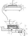
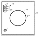
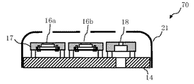
図1は、実施の形態1におけるステージ機構の構成の一例を示す正面構成図である。図2は、実施の形態1におけるステージ機構の構成の一例を示す上面図である。図1において、ステージ機構105は、複数段のサブステージを有する。複数段のサブステージとして、図1の例では、x方向(電子ビーム(図1ではマルチ1次電子ビーム20)の軌道中心軸に直交する平面上の1軸方向)の移動が可能なxステージとy方向(x軸に直交する上述した平面上の他の1軸方向)の移動が可能なyステージとを組み合わせたXYステージ60と、z方向(電子ビームの軌道中心軸方向)の移動が可能なzステージとθ方向(z軸回りの回転方向)の移動が可能なθステージとを組み合わせたzθステージ62と、基板等を載置する台座ステージ64とが、積層される構成を示している。また、図1及び図2に示すように、台座ステージ64の中央部の領域(第1の領域)には、電子ビームが照射される対象となる基板101(試料)が配置される。具体的には、台座ステージ64の中央部の領域には、静電チャック機構104が配置される。そして、静電チャック機構104上に基板101が載置され、静電チャックにより基板101の裏面が吸着され、基板101が固定される。
FIG. 1 is a front configuration diagram showing an example of the configuration of the stage mechanism according to the first embodiment. FIG. 2 is a top view showing an example of the configuration of the stage mechanism according to the first embodiment. In FIG. 1, the
基板101には、露光用マスク基板、及びシリコンウェハ等の半導体基板が含まれる。図1及び図2の例では、基板101が半導体基板である場合を示している。基板101が半導体基板である場合、半導体基板には複数のチップ(ウェハダイ)が形成されている。基板101が露光用マスク基板である場合、露光用マスク基板には、チップパターンが形成されている。チップパターンは、複数の図形パターンによって構成される。かかる露光用マスク基板に形成されたチップパターンが半導体基板上に複数回露光転写されることで、半導体基板には複数のチップ(ウェハダイ)が形成されることになる。以下、基板101が半導体基板である場合を主として説明する。基板101は、例えば、パターン形成面を上側に向けてステージ機構105に配置される。
The
図1及び図2に示すように、台座ステージ64の中央部の領域とは異なる中央部から外れた周辺の領域(第2の領域)には、マーク機構70が配置される。マーク機構70には、例えば、少なくとも1つのマーク16が配置される。図1及び図2の例では、2つのマーク16a,16bと1つのファラディーカップ13とが配置される場合を示している。また、zθステージ62のz方向(上下方向)へと移動しない固定領域には、台座ステージ64を貫通した、z方向へと移動しない固定マーク15が配置される。マーク16a,16b表面の高さ位置は、静電チャック機構104に静電チャックされた状態での基板101表面と同じ高さ位置に調整されている。マーク16と固定マーク15は、台座ステージ64上の領域の両側に分かれて配置されると好適である。zθステージ62をz方向に移動させながらマーク16と固定マーク15との高さ位置を合わせることで、台座ステージ64を水平に保つと共に、基板101表面の高さ位置を基準となる固定マーク15表面高さ位置に合わせることができる。
As shown in FIGS. 1 and 2, the
マーク機構70は、支持台11、支柱12、基台14、少なくとも1つのマーク16、少なくとも1つのマーク台17、ファラディーカップ13、及びシールドカバー21を有している。台座ステージ64のマーク機構70が配置される領域には開口部66が形成される。そして、開口部66を跨ぐように、台座ステージ64上に導電性の支持台11が配置される。支持台11上には、複数(例えば2本)の絶縁性の支柱12が配置される。言い換えれば、絶縁性の支柱12は、支持台11を介してステージ機構105(台座ステージ64)上に配置される。そして、ステージ機構105(台座ステージ64)と支柱12との間に支持台11が配置される。ステージ機構105にはグランド(GND)電位が印加される。そして、支持台11は、台座ステージ64上に接触して配置されるので台座ステージ64を介してGND電位が印加される。
The
そして、複数の絶縁性の支柱12によって導電性の基台14が支持される。基台14上には、マーク機構70に配置されるすべてのマーク台17及びファラディーカップ13のアパーチャプレート18が配置される。アパーチャプレート18下の基台14上の領域には、測定される電子ビームの通過孔が形成される。各マーク台17上にはそれぞれマーク16が配置される。言い換えれば、基台14は、マーク機構70に配置されるすべてのマーク16及びマーク以外の例えばファラディーカップ13のアパーチャプレート18における共通ベースとして機能する。各マーク台17或いは及び各マーク16は、突起部を有する。突起部として、例えば、マーク16をマーク台17に固定するためのネジ及びマーク台17の角部等が該当し得る。同様に、突起部として、例えば、アパーチャプレート18の角部等が該当し得る。基台14は、ステージ側に対して、これらの突起部を覆うようにマーク機構70に配置されるすべてのマーク16及びマーク以外の例えばファラディーカップ13のアパーチャプレート18を配置する。基台14上に配置される少なくとも1つのマーク16と重なる支持台11の領域には開口部67が形成される。そして、基台14の裏面側(ステージ側)には、支持台11の開口部67及び台座ステージ64の開口部66を通る電極73が配置される。
Then, the
ここで、基板101に電子ビームを照射するにあたり、基板101上での電子ビームのランディングエネルギーを適切な状態にするために、基板101には負のリターディング電位が印加される。台座ステージ64上に配置されたマーク16及びファラディーカップ13用のアパーチャプレート18にも基板101と同じ照射条件を生成するために負のリターディング電位を印加する。そのため、電極73には、基台14に負の電位を印加する例えば1本のケーブル71が接続される。図1及び図2の例では、共通ベースとなる基台14上に、マーク台17及びアパーチャプレート18が配置されるので、共通のケーブル71を通して基台14に負の電位を印加することで、基台14を介して基台14上のすべてのマーク16(少なくとも1つのマーク部)に負の電位が印加される。同様に、基台14を介して基台14上のすべてのアパーチャプレート18に負の電位が印加される。これにより、基板101に印加するリターディング電位と同じ負の電位を電子ビームが照射されるマーク16及びアパーチャプレート18に印加できる。一方、ファラディーカップ13用の検出器19は、アパーチャプレート18と重なる位置で、グランド電位に印加される支持台11上に配置される。
Here, when irradiating the
シールドカバー21は、マーク機構70に配置されるすべてのマーク16(少なくとも1つのマーク部)に対して基台14とは反対側から、電子ビームの通過領域を残してマーク機構70に配置されるすべてのマーク16(少なくとも1つのマーク部)を覆う。図1及び図2の例では、シールドカバー21は、電子ビームの通過領域を残してマーク機構70に配置されるアパーチャプレート18を覆う。図1及び図2の例では、シールドカバー21は、マーク台17(及びマーク16)及びアパーチャプレート18の上方及び側方を覆う。シールドカバー21は、上面と側面との繋ぎを放電が生じ易い角が生じないようになだらかな曲線によって形成すると好適である。シールドカバー21には、基台14を介して負の電位が印加される。
The
よって、基台14とシールドカバー21とに囲まれた部分は、同じ負の電位に帯電することになる。そして、絶縁性の支柱12を挟んで、支持台11、支持台11上の検出器19、及び台座ステージ64は、GND電位に維持されることになる。
Therefore, the portion surrounded by the
台座ステージ64の裏面には、端子台機構72が配置される。端子台機構72が配置される場所は、台座ステージ64の裏面に限るものではない。ステージ機構105の複数段のサブステージのうちのいずれかの下面に配置されればよい。例えば、zθステージ62の裏面であっても良い。端子台機構72は、端子台74、支柱77、及び端子台シールドカバー76を有している。端子台74は、絶縁性の支柱77を挟んで台座ステージ64の裏面に配置される。端子台74には、基台14に負の電位を印加するケーブル71の一端が接続される。また、検出器19から延びる配線も接続されても良い。端子台74は、ステージ機構105の外側から延びるケーブル75とケーブル71とを電気的に接続する。ケーブル75には、負の電位が印加される。ここでは、基板101に印加されるリターディング電位(例えば、−15kV)の電位が印加される。端子台シールドカバー76は、端子台74を下面側から覆う。よって、端子台74における突起部全体を端子台シールドカバー76が覆うことができる。端子台74における突起部として、例えば、ケーブル71,75を端子台74に固定するネジ等が該当する。
A
よって、端子台74と端子台シールドカバー76とに囲まれた部分は、同じ負の電位に帯電することになる。そして、絶縁性の支柱77を挟んで、台座ステージ64は、GND電位に維持されることになる。
Therefore, the portion surrounded by the
ここで、上述したように、リターディング電位が印加されるマークやファラディーカップのアパーチャプレートには、突起物となる部品等が使用されるため、構造物間の狭い空間において放電を起こしやすいといった問題があった。 Here, as described above, since parts such as protrusions are used for the mark to which the retarding potential is applied and the aperture plate of the faradi cup, it is said that electric discharge is likely to occur in a narrow space between structures. There was a problem.
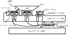
図3は、実施の形態1の比較例1におけるステージ機構と周辺構成との一例を示す図である。図3では、マーク機構部分を拡大して示している。図3において、実施の形態1の比較例1では、複数のマーク台がそれぞれ個別に台座ステージ上に配置される。具体的には、それぞれ個別に導電性のマークベースを台座ステージ上に配置する。そして、マークベース毎に、絶縁性の支柱を介してマーク台が配置され、マーク台上にマークが配置される。ファラディーカップについても、検出器ベースが個別に台座ステージ上に配置される。そして、検出器ベースにはファラディーカップ用の検出器が配置される。検出器ベース上には、絶縁性の支柱を介してファラディーカップ用のアパーチャプレートが配置される。図3に示す比較例1では、複数のマークが個別に台座ステージ上に配置されるので、マークに負の電位(リターディング電位)を印加するケーブルがそれぞれ必要となる。また、複数のマークベースを配置するために、台座ステージには、マーク毎にケーブルを通すための開口部が形成される。各ケーブルは、台座ステージの裏面に配置される端子台に接続され、ステージ機構の外部の電源へと接続される。 FIG. 3 is a diagram showing an example of the stage mechanism and the peripheral configuration in Comparative Example 1 of the first embodiment. In FIG. 3, the mark mechanism portion is enlarged and shown. In FIG. 3, in Comparative Example 1 of the first embodiment, a plurality of mark stands are individually arranged on the pedestal stage. Specifically, conductive mark bases are individually arranged on the pedestal stage. Then, for each mark base, a mark base is arranged via an insulating support column, and the mark is arranged on the mark base. For the Faraday Cup, the detector bases are individually placed on the pedestal stage. Then, a detector for the Faraday cup is arranged on the detector base. An aperture plate for the Faraday cup is placed on the detector base via an insulating column. In Comparative Example 1 shown in FIG. 3, since a plurality of marks are individually arranged on the pedestal stage, cables for applying a negative potential (retarding potential) to the marks are required. Further, in order to arrange a plurality of mark bases, an opening for passing a cable is formed in each mark on the pedestal stage. Each cable is connected to a terminal block arranged on the back surface of the pedestal stage, and is connected to an external power source of the stage mechanism.
よって、各マーク台及びマークとアパーチャプレートには、それぞれ別々のケーブルによって印加された負の電位に帯電することになる。そして、絶縁性の支柱を挟んで、各マークベース、検出器ベース、検出器ベース上の検出器、及び台座ステージは、GND電位に維持されることになる。そして、絶縁性の支柱を挟んで、裏面の端子台は負の電位に帯電することになる。 Therefore, each mark base and the mark and the aperture plate are charged with the negative potential applied by the separate cables. Then, the mark base, the detector base, the detector on the detector base, and the pedestal stage are maintained at the GND potential with the insulating support column interposed therebetween. Then, the terminal block on the back surface is charged with a negative potential across the insulating column.
ここで、図3に示す比較例1では、各マーク台の角部が突起部となって、台座ステージとの間に放電が生じ得る。同様に、各マーク台のマークを取り付けるためのネジ等が突起部となって、マークベースとの間に放電が生じ得る。また、台座ステージにはマーク毎にケーブルを通すための開口部が形成されるため、設置スペースが制限される中でそれぞれの開口部の径サイズは小さくせざるを得ない。そのために、マーク毎にマークとケーブルとを繋ぐ電極と台座ステージの開口部内壁との間に放電が生じ得る。また、各マーク台の角部が突起部となって、電子ビームを照射する電子鏡筒の下部に位置する、GND電位が印加された対物レンズ207との間に放電が生じ得る。また、端子台では、端子台のネジ等が突起部となって、台座ステージの下部に位置する、GND電位が印加されたzθステージとの間に放電が生じ得る。以上のように、図3に示す比較例1では、様々な個所で放電が生じ得るといった問題があった。
Here, in Comparative Example 1 shown in FIG. 3, a corner portion of each mark stand becomes a protrusion, and an electric discharge may occur between the mark stand and the pedestal stage. Similarly, a screw or the like for attaching the mark of each mark base becomes a protrusion, and an electric discharge may occur between the mark base and the mark base. Further, since the pedestal stage is formed with openings for passing cables for each mark, the diameter size of each opening must be reduced while the installation space is limited. Therefore, a discharge may occur between the electrode connecting the mark and the cable for each mark and the inner wall of the opening of the pedestal stage. Further, a corner portion of each mark base serves as a protrusion, and a discharge may occur between the mark base and the
これに対して、実施の形態1では、図1及び図2に示すように、基台14がマーク台17(及びマーク16)及びアパーチャプレート18の突起部全体をステージ側に対して覆っている。そのため、ステージ側に突起部を晒さずに済ますことができる。よって、負の電位に帯電する突起部とGND電位に帯電する支持台11及び台座ステージ64との間での放電を抑制或いは低減できる。
On the other hand, in the first embodiment, as shown in FIGS. 1 and 2, the base 14 covers the entire protrusions of the mark base 17 (and mark 16) and the
さらに、基台14を介してマーク機構70に配置されるすべてのマーク16及びすべてのアパーチャプレート18に負の電位を印加するため、基台14に対して1組の電極73及びケーブル71があれば足りる。よって、開口部67及び開口部66の数を減らすことができる。そのため、開口部67及び開口部66のサイズを、複数の開口部67及び複数の開口部66を形成する場合に比べて大きくできる。言い換えれば、負の電位に帯電する電極73及びケーブル71に対して、GND電位に帯電する支持台11及び台座ステージ64までの距離(空間)を離す(大きく)できる。その結果、電極73(或いはケーブル71)と支持台11との間での放電、及び電極73(或いはケーブル71)と台座ステージ64との間での放電を抑制或いは低減できる。
Further, in order to apply a negative potential to all the marks 16 and all the
さらに、実施の形態1では、シールドカバー21が、電子ビームの通過領域を残してマーク機構70に配置される各マーク台17(及び各マーク16)及びアパーチャプレート18の上方及び側方を覆う。よって、電子ビームを照射する電子鏡筒の下部に位置する、GND電位が印加された対物レンズ207側に突起部を晒さないようにできる。よって、上方側において、負の電位に帯電する突起部とGND電位に帯電する対物レンズ207との間での放電を抑制或いは低減できる。さらに、シールドカバー21によって、側面方向においても突起部を晒さないようにできる。よって、側面方向において、負の電位に帯電する突起部とGND電位に帯電する台座ステージ64との間での放電を抑制或いは低減できる。
Further, in the first embodiment, the
また、端子台機構72においては、端子台74における突起部全体を端子台シールドカバー76が覆う。よって、台座ステージ64の下部に位置する、GND電位が印加されたzθステージ62側に、突起部を晒さないようにできる。よって、端子台74における突起部とGND電位が印加されたzθステージ62との間での放電を抑制或いは低減できる。
Further, in the
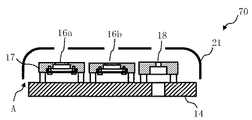
図4は、実施の形態1の比較例2におけるシールドカバーの配置構成を示す図である。図4の例では、シールドカバー21の側面が、基台14の側面を覆わず、かつ基台14の側面よりも出っ張るように配置する場合を示している。かかる場合、シールドカバー21の下端部(A)が突起部となって放電を誘発し兼ねない。
FIG. 4 is a diagram showing an arrangement configuration of a shield cover in Comparative Example 2 of the first embodiment. In the example of FIG. 4, the case where the side surface of the
これに対して、実施の形態1では、図1に示したように、シールドカバー21の下端部が基台14表面まで実質的に届き、かつシールドカバー21の側面と、基台14の側壁とが実質的に同一面になるように構成する場合を示した。これにより、シールドカバー21の下部端を突起物として、台座ステージ64側に晒さないようにできる。その結果、側面方向において、負の電位に帯電する突起部とGND電位に帯電する台座ステージ64との間での放電を抑制或いは低減できる。但し、シールドカバー21が覆う態様は、これに限るものではない。
On the other hand, in the first embodiment, as shown in FIG. 1, the lower end portion of the
図5は、実施の形態1の変形例におけるシールドカバーの配置構成を示す図である。図5の例では、シールドカバー21が基台14の側壁も覆う構成を示している。その他の構成は、図1と同様である。図4の例に示すように、シールドカバー21が基台14の側壁まで覆うように構成しても好適である。かかる場合でも負の電位に帯電する突起部を側面方向に晒さないようにできる。
FIG. 5 is a diagram showing an arrangement configuration of a shield cover in a modified example of the first embodiment. In the example of FIG. 5, the
次に、実施の形態1のステージ機構105を搭載した検査装置について説明する。
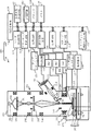
図6は、実施の形態1における検査装置の構成を示す構成図である。図6において、基板101に形成されたパターンを検査する検査装置100は、マルチ電子ビーム検査装置の一例である。検査装置100は、画像取得機構150、及び制御系回路160を備えている。画像取得機構150は、電子ビームカラム102(電子鏡筒)及び検査室103を備えている。電子ビームカラム102内には、電子銃201、電磁レンズ202、成形アパーチャアレイ基板203、電磁レンズ205、一括ブランキング偏向器212、制限アパーチャ基板213、電磁レンズ206、電磁レンズ207(対物レンズ)、主偏向器208、副偏向器209、ビームセパレーター214、偏向器218、電磁レンズ224、及びマルチ検出器222が配置されている。電子銃201、電磁レンズ202、成形アパーチャアレイ基板203、電磁レンズ205、一括ブランキング偏向器212、制限アパーチャ基板213、電磁レンズ206、電磁レンズ207(対物レンズ)、主偏向器208、及び副偏向器209によって1次電子光学系151を構成する。また、電磁レンズ207、ビームセパレーター214、偏向器218、及び電磁レンズ224によって2次電子光学系152を構成する。
Next, an inspection device equipped with the
FIG. 6 is a configuration diagram showing the configuration of the inspection device according to the first embodiment. In FIG. 6, the
検査室103内には、上述したマーク機構70及び端子台機構72が搭載されたステージ機構105が配置される。ステージ機構105上には、検査対象となる基板101が配置される。基板101は、ステージ機構105上に搭載された静電チャック機構上に載置され、静電チャックにより裏面が吸着される。基板101には、露光用マスク基板、及びシリコンウェハ等の半導体基板が含まれる。基板101が半導体基板である場合、半導体基板には複数のチップ(ウェハダイ)が形成されている。基板101が露光用マスク基板である場合、露光用マスク基板には、チップパターンが形成されている。チップパターンは、複数の図形パターンによって構成される。かかる露光用マスク基板に形成されたチップパターンが半導体基板上に複数回露光転写されることで、半導体基板には複数のチップ(ウェハダイ)が形成されることになる。以下、基板101が半導体基板である場合を主として説明する。基板101は、例えば、パターン形成面を上側に向けてステージ機構105に配置される。また、ステージ機構105上には、検査室103の外部に配置されたレーザ測長システム122から照射されるレーザ測長用のレーザ光を反射するミラー216が配置されている。
In the
また、検査室103上には、基板101の高さ位置を測定するzセンサ214が配置される。zセンサ214の投光器から基板101にレーザ光を照射し、基板101から反射された反射光を受光器で受光することで、基板101表面の高さ位置を測定できる。
Further,
また、マルチ検出器222は、電子ビームカラム102の外部で検出回路106に接続される。検出回路106は、チップパターンメモリ123に接続される。
Further, the multi-detector 222 is connected to the detection circuit 106 outside the
制御系回路160では、検査装置100全体を制御する制御計算機110が、バス120を介して、位置回路107、比較回路108、参照画像作成回路112、ステージ制御回路114、レンズ制御回路124、ブランキング制御回路126、偏向制御回路128、リターディング電位印加回路170、磁気ディスク装置等の記憶装置109、モニタ117、メモリ118、及びプリンタ119に接続されている。また、偏向制御回路128は、DAC(デジタルアナログ変換)アンプ144,146,148に接続される。DACアンプ146は、主偏向器208に接続され、DACアンプ144は、副偏向器209に接続される。DACアンプ148は、偏向器218に接続される。
In the
また、基板101は、リターディング電位印加回路170に電気的に接続され、リターディング電位印加回路170は、基板101に負のリターディング電位Vrを印加する。また、端子台機構72を介して、マーク機構70は、リターディング電位印加回路170に電気的に接続され、リターディング電位印加回路170は、マーク機構70に、基板101と同じ負のリターディング電位Vrを印加する。
Further, the
また、チップパターンメモリ123は、比較回路108に接続されている。また、ステージ機構105は、ステージ制御回路114の制御の下に駆動機構142により駆動される。上述したように、ステージ機構105の複数段のサブステージにより、x,y,z,θ方向に台座ステージ64を移動させることができる。そして、ステージ機構105のx,y方向の移動位置はレーザ測長システム122により測定され、位置回路107に供給される。レーザ測長システム122は、ミラー216からの反射光を受光することによって、レーザ干渉法の原理でステージ機構105の位置を測長する。ステージ座標系は、例えば、マルチ1次電子ビーム20の軌道中心軸(光軸)に直交する面に対して、X方向、Y方向、θ方向が設定される。
Further, the
電磁レンズ202、電磁レンズ205、電磁レンズ206、電磁レンズ207(対物レンズ)、電磁レンズ224、及びビームセパレーター214は、レンズ制御回路124により制御される。また、一括ブランキング偏向器212は、2極以上の電極により構成され、電極毎に図示しないDACアンプを介してブランキング制御回路126により制御される。副偏向器209は、4極以上の電極により構成され、電極毎にDACアンプ144を介して偏向制御回路128により制御される。主偏向器208は、4極以上の電極により構成され、電極毎にDACアンプ146を介して偏向制御回路128により制御される。偏向器218は、4極以上の電極により構成され、電極毎にDACアンプ148を介して偏向制御回路128により制御される。
The
電子銃201には、図示しない高圧電源回路が接続され、電子銃201内の図示しないフィラメント(カソード)と引出電極(アノード)間への高圧電源回路からの加速電圧の印加と共に、別の引出電極(ウェネルト)の電圧の印加と所定の温度のカソードの加熱によって、カソードから放出された電子群が加速させられ、電子ビーム200となって放出される。
A high-voltage power supply circuit (not shown) is connected to the
ここで、図6では、実施の形態1を説明する上で必要な構成を記載している。検査装置100にとって、通常、必要なその他の構成を備えていても構わない。
Here, FIG. 6 describes a configuration necessary for explaining the first embodiment. The
まず、ステージ機構105のマーク16と固定マーク15との高さ位置を合わせる。各マークの高さ位置は、zセンサ214によって測定すればよい。マーク16と固定マーク15との高さ位置を合わせることで、基板101を配置する台座ステージを水平に調整できると共に、基板101表面高さ位置を固定マーク15表面高さ位置に合わせることができる。実際のスキャン工程においては、zセンサ214で予め測定しておいた基板101表面の高さ分布に応じて、zθステージ62により基板101表面の高さ位置を基準高さ位置にダイナミックに調整すればよい。
First, the height positions of the mark 16 and the fixed
また、貴台14を介してマーク16にリターディング電位Vrが印加された状態で、マーク16を電子ビーム(マルチ1次電子ビーム20)でスキャンする。そして、マーク16から放出された2次電子をマルチ検出器222で検出することで、マーク画像を得ることができる。マーク画像を用いて、1次電子光学系151及び/或いは2次電子光学系152の調整(キャリブレーション)を行う。以上のようにして、高さ位置の調整(キャリブレーション)と光学系の調整とを行った上で、実際の検査処理を実施する。
Further, the mark 16 is scanned with an electron beam (multi-primary electron beam 20) in a state where the retarding potential Vr is applied to the mark 16 via the
スキャン工程として、1次電子光学系151は、被検査基板101にリターディング電位Vrが印加された状態で、被検査基板101を電子ビーム(マルチ1次電子ビーム20)で照射する。言い換えれば、画像取得機構150は、マルチ1次電子ビーム20を用いて被検査基板101に形成されたパターンの2次電子画像を取得する。具体的には以下のように動作する。
As a scanning step, the primary
図7は、実施の形態1における半導体基板に形成される複数のチップ領域の一例を示す図である。図7において、基板101が半導体基板(ウェハ)である場合、半導体基板(ウェハ)の検査領域330には、複数のチップ(ウェハダイ)332が2次元のアレイ状に形成されている。各チップ332には、露光用マスク基板に形成された1チップ分のマスクパターンが図示しない露光装置(ステッパ)によって例えば1/4に縮小されて転写されている。1チップ分のマスクパターンは、一般に、複数の図形パターンにより構成される。各チップ332の領域は、例えばy方向に向かって所定の幅で複数のストライプ領域32に分割される。画像取得機構150によるスキャン動作は、例えば、ストライプ領域32毎に実施される。例えば、−x方向にステージ機構105を移動させながら、相対的にx方向にストライプ領域32のスキャン動作を進めていく。各ストライプ領域32は、長手方向に向かって複数の矩形領域33に分割される。対象となる矩形領域33へのビームの移動は、主偏向器208によるマルチ1次電子ビーム20全体での一括偏向によって行われる。
FIG. 7 is a diagram showing an example of a plurality of chip regions formed on the semiconductor substrate according to the first embodiment. In FIG. 7, when the
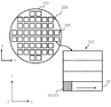
図8は、実施の形態1における成形アパーチャアレイ基板の構成を示す概念図である。図8において、成形アパーチャアレイ基板203には、2次元状の横(x方向)m1列×縦(y方向)n1段(m1,n1は2以上の整数)の穴(開口部)22がx,y方向に所定の配列ピッチで形成されている。図8の例では、23×23の穴(開口部)22が形成されている場合を示している。各穴22は、共に同じ寸法形状の矩形で形成される。或いは、同じ外径の円形であっても構わない。これらの複数の穴22を電子ビーム200の一部がそれぞれ通過することで、マルチ1次電子ビーム20が形成されることになる。次に、2次電子画像を取得する場合における画像取得機構150の動作について説明する。
FIG. 8 is a conceptual diagram showing the configuration of the molded aperture array substrate according to the first embodiment. In FIG. 8, the molded
電子銃201(放出源)から放出された電子ビーム200は、電磁レンズ202によって屈折させられ、成形アパーチャアレイ基板203全体を照明する。成形アパーチャアレイ基板203には、図8に示すように、複数の穴22(開口部)が形成され、電子ビーム200は、すべての複数の穴22が含まれる領域を照明する。複数の穴22の位置に照射された電子ビーム200の各一部が、かかる成形アパーチャアレイ基板203の複数の穴22をそれぞれ通過することによって、マルチ1次電子ビーム20が形成される。
The
形成されたマルチ1次電子ビーム20は、電磁レンズ205、及び電磁レンズ206によってそれぞれ屈折させられ、中間像およびクロスオーバーを繰り返しながら、マルチ1次電子ビーム20の各ビームの中間像面(像面共役位置)に配置されたビームセパレーター214を通過して電磁レンズ207(対物レンズ)に進む。
The formed
マルチ1次電子ビーム20が電磁レンズ207(対物レンズ)に入射すると、電磁レンズ207は、マルチ1次電子ビーム20を基板101にフォーカスする。対物レンズ207により基板101(試料)面上に焦点が合わされ(合焦され)たマルチ1次電子ビーム20は、主偏向器208及び副偏向器209によって一括して偏向され、各ビームの基板101上のそれぞれの照射位置に照射される。なお、一括ブランキング偏向器212によって、マルチ1次電子ビーム20全体が一括して偏向された場合には、制限アパーチャ基板213の中心の穴から位置がはずれ、制限アパーチャ基板206によってマルチ1次電子ビーム20全体が遮蔽される。一方、一括ブランキング偏向器212によって偏向されなかったマルチ1次電子ビーム20は、図1に示すように制限アパーチャ基板206の中心の穴を通過する。かかる一括ブランキング偏向器212のON/OFFによって、ブランキング制御が行われ、ビームのON/OFFが一括制御される。このように、制限アパーチャ基板206は、一括ブランキング偏向器212によってビームOFFの状態になるように偏向されたマルチ1次電子ビーム20を遮蔽する。そして、ビームONになってからビームOFFになるまでに形成された、制限アパーチャ基板206を通過したビーム群により、画像取得用のマルチ1次電子ビーム20が形成される。
When the
基板101の所望する位置にマルチ1次電子ビーム20が照射されると、かかるマルチ1次電子ビーム20が照射されたことに起因して基板101からマルチ1次電子ビーム20の各ビームに対応する、反射電子を含む2次電子の束(マルチ2次電子ビーム300)が放出される。
When the
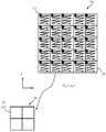
図9は、実施の形態1におけるマルチビームのスキャン動作を説明するための図である。図9の例では、例えば、5×5列のマルチ1次電子ビーム20の場合を示している。1回のマルチ1次電子ビーム20の照射で照射可能な照射領域34は、(基板101面上におけるマルチ1次電子ビーム20のx方向のビーム間ピッチにx方向のビーム数を乗じたx方向サイズ)×(基板101面上におけるマルチ1次電子ビーム20のy方向のビーム間ピッチにy方向のビーム数を乗じたy方向サイズ)で定義される。そして、マルチ1次電子ビーム20を構成する各1次電子ビーム10は、自身のビームが位置するx方向のビーム間ピッチとy方向のビーム間ピッチとで囲まれるサブ照射領域29内に照射され、当該サブ照射領域29内を走査(スキャン動作)する。各1次電子ビーム10は、互いに異なるいずれかのサブ照射領域29を担当することになる。そして、各ショット時に、各1次電子ビーム10は、担当サブ照射領域29内の同じ位置を照射することになる。サブ照射領域29内の1次電子ビーム10の移動は、副偏向器209によるマルチ1次電子ビーム20全体での一括偏向によって行われる。かかる動作を繰り返し、1つの1次電子ビーム10で1つのサブ照射領域29内を順に照射していく。
FIG. 9 is a diagram for explaining a multi-beam scanning operation according to the first embodiment. In the example of FIG. 9, for example, the case of a
基板101から放出されたマルチ2次電子ビーム300は、電磁レンズ207を通って、ビームセパレーター214に進む。
The
ここで、ビームセパレーター214はマルチ1次電子ビーム20の中心ビームが進む方向(軌道中心軸)に直交する面上において電界と磁界を直交する方向に発生させる。電界は電子の進行方向に関わりなく同じ方向に力を及ぼす。これに対して、磁界はフレミング左手の法則に従って力を及ぼす。そのため電子の侵入方向によって電子に作用する力の向きを変化させることができる。ビームセパレーター214に上側から侵入してくるマルチ1次電子ビーム20には、電界による力と磁界による力が打ち消し合い、マルチ1次電子ビーム20は下方に直進する。これに対して、ビームセパレーター214に下側から侵入してくるマルチ2次電子ビーム300には、電界による力と磁界による力がどちらも同じ方向に働き、マルチ2次電子ビーム300は斜め上方に曲げられ、マルチ1次電子ビーム20から分離する。
Here, the
斜め上方に曲げられ、マルチ1次電子ビーム20から分離したマルチ2次電子ビーム300は、偏向器218によって、さらに曲げられ、電磁レンズ224によって、屈折させられながらマルチ検出器222に投影される。マルチ検出器222は、投影されたマルチ2次電子ビーム300を検出する。マルチ検出器222は、例えば図示しないダイオード型の2次元センサを有する。そして、マルチ1次電子ビーム20の各ビームに対応するダイオード型の2次元センサ位置において、マルチ2次電子ビーム300の各2次電子がダイオード型の2次元センサに衝突して、電子を発生し、2次電子画像データを画素毎に生成する。マルチ検出器222にて検出された強度信号は、検出回路106に出力される。
The
ここで、ステージ機構105が連続移動しながらマルチ1次電子ビーム20を基板101に照射する場合、マルチ1次電子ビーム20の照射位置がステージ機構105の移動に追従するように主偏向器208によって一括偏向によるトラッキング動作が行われる。そのため、マルチ2次電子ビーム300の放出位置がマルチ1次電子ビーム20の軌道中心軸に対して刻々と変化する。同様に、サブ照射領域29内をスキャンする場合に、各2次電子ビームの放出位置は、サブ照射領域29内で刻々と変化する。このように放出位置が変化した各2次電子ビームをマルチ検出器222の対応する検出領域内に照射させるように、偏向器218は、マルチ2次電子ビーム300を一括偏向する。
Here, when the
2次電子画像の取得は、上述したように、マルチ1次電子ビーム20を照射して、マルチ1次電子ビーム20の照射に起因して基板101から放出される反射電子を含むマルチ2次電子ビーム300をマルチ検出器222で検出する。マルチ検出器222によって検出された各サブ照射領域29内の画素毎の2次電子の検出データ(測定画像データ:2次電子画像データ:被検査画像データ)は、測定順に検出回路106に出力される。検出回路106内では、図示しないA/D変換器によって、アナログの検出データがデジタルデータに変換され、チップパターンメモリ123に格納される。そして、得られた2次電子画像データ(2次電子画像1のデータ)は、位置回路107からの各位置を示す情報と共に、比較回路108に出力される。
As described above, the secondary electron image is obtained by irradiating the
上述した各ストライプ領域32の幅は、照射領域34のy方向サイズと同様、或いはスキャンマージン分狭くしたサイズに設定すると好適である。図7の例では、照射領域34が矩形領域33と同じサイズの場合を示している。但し、これに限るものではない。照射領域34が矩形領域33よりも小さくても良い。或いは大きくても構わない。そして、1つのサブ照射領域29のスキャンが終了したら、主偏向器208によるマルチ1次電子ビーム20全体での一括偏向によって照射位置が同じストライプ領域32内の隣接する矩形領域33へと移動する。かかる動作を繰り返し、ストライプ領域32内を順に照射していく。1つのストライプ領域32のスキャンが終了したら、ステージ機構105の移動或いは/及び主偏向器208によるマルチ1次電子ビーム20全体での一括偏向によって照射領域34が次のストライプ領域32へと移動する。以上のように各1次電子ビーム10の照射によってサブ照射領域29毎のスキャン動作および2次電子画像の取得が行われる。これらのサブ照射領域29毎の2次電子画像を組み合わせることで、矩形領域33の2次電子画像、ストライプ領域32の2次電子画像、或いはチップ332の2次電子画像が構成される。また、実際に画像比較を行う場合には、図9に示すように、各矩形領域33内のサブ照射領域29をさらに複数のフレーム領域30に分割して、フレーム領域30毎のフレーム画像31について比較することになる。
It is preferable that the width of each of the
図10は、実施の形態1における比較回路内の構成の一例を示す構成図である。図10において、比較回路108内には、磁気ディスク装置等の記憶装置50,52,56、フレーム画像作成部54、位置合わせ部57、及び比較部58が配置される。フレーム画像作成部54、位置合わせ部57、及び比較部58といった各「〜部」は、処理回路を含み、その処理回路には、電気回路、コンピュータ、プロセッサ、回路基板、量子回路、或いは、半導体装置等が含まれる。また、各「〜部」は、共通する処理回路(同じ処理回路)を用いてもよい。或いは、異なる処理回路(別々の処理回路)を用いても良い。フレーム画像作成部54、位置合わせ部57、及び比較部58内に必要な入力データ或いは演算された結果はその都度図示しないメモリ、或いはメモリ118に記憶される。
FIG. 10 is a configuration diagram showing an example of the configuration in the comparison circuit according to the first embodiment. In FIG. 10,
比較回路108内に転送された測定画像データ(ビーム画像)は、記憶装置50に格納される。
The measurement image data (beam image) transferred into the
そして、フレーム画像作成部54は、各1次電子ビーム10のスキャン動作によって取得されたサブ照射領域29の画像データをさらに分割した複数のフレーム領域30のフレーム領域30毎のフレーム画像31を作成する。なお、各フレーム領域30は、画像の抜けが無いように、互いにマージン領域が重なり合うように構成されると好適である。作成されたフレーム画像31は、記憶装置56に格納される。
Then, the frame
参照画像作成工程として、参照画像作成回路112は、基板101に形成された複数の図形パターンの元になる設計データに基づいて、フレーム領域30毎に、フレーム画像31に対応する参照画像を作成する。具体的には、以下のように動作する。まず、記憶装置109から制御計算機110を通して設計パターンデータを読み出し、この読み出された設計パターンデータに定義された各図形パターンを2値ないしは多値のイメージデータに変換する。
As a reference image creation step, the reference image creation circuit 112 creates a reference image corresponding to the
上述したように、設計パターンデータに定義される図形は、例えば長方形や三角形を基本図形としたもので、例えば、図形の基準位置における座標(x、y)、辺の長さ、長方形や三角形等の図形種を区別する識別子となる図形コードといった情報で各パターン図形の形、大きさ、位置等を定義した図形データが格納されている。 As described above, the figure defined in the design pattern data is, for example, a rectangle or a triangle as a basic figure, for example, the coordinates (x, y) at the reference position of the figure, the length of the side, the rectangle or the triangle, etc. Graphical data that defines the shape, size, position, etc. of each pattern graphic is stored with information such as a graphic code that serves as an identifier that distinguishes the graphic types of.
かかる図形データとなる設計パターンデータが参照画像作成回路112に入力されると図形ごとのデータにまで展開し、その図形データの図形形状を示す図形コード、図形寸法などを解釈する。そして、所定の量子化寸法のグリッドを単位とするマス目内に配置されるパターンとして2値ないしは多値の設計パターン画像データに展開し、出力する。言い換えれば、設計データを読み込み、検査領域を所定の寸法を単位とするマス目として仮想分割してできたマス目毎に設計パターンにおける図形が占める占有率を演算し、nビットの占有率データを出力する。例えば、1つのマス目を1画素として設定すると好適である。そして、1画素に1/28(=1/256)の分解能を持たせるとすると、画素内に配置されている図形の領域分だけ1/256の小領域を割り付けて画素内の占有率を演算する。そして、8ビットの占有率データとなる。かかるマス目(検査画素)は、測定データの画素に合わせればよい。 When the design pattern data to be the graphic data is input to the reference image creation circuit 112, it is expanded to the data for each graphic, and the graphic code, the graphic dimension, etc. indicating the graphic shape of the graphic data are interpreted. Then, it is developed into binary or multi-valued design pattern image data as a pattern arranged in a grid having a grid of predetermined quantization dimensions as a unit and output. In other words, the design data is read, the inspection area is virtually divided into squares with a predetermined dimension as a unit, the occupancy rate of the figure in the design pattern is calculated for each square, and the n-bit occupancy rate data is obtained. Output. For example, it is preferable to set one square as one pixel. Then, when to have a resolution of 1/2 8 (= 1/256) to 1 pixel, the occupancy rate of the pixel allocated the small area region amount corresponding 1/256 of figures are arranged in a pixel Calculate. Then, it becomes 8-bit occupancy rate data. Such squares (inspection pixels) may be matched with the pixels of the measurement data.
次に、参照画像作成回路112は、図形のイメージデータである設計パターンの設計画像データに、所定のフィルタ関数を使ってフィルタ処理を施す。これにより、画像強度(濃淡値)がデジタル値の設計側のイメージデータである設計画像データをマルチ1次電子ビーム20の照射によって得られる像生成特性に合わせることができる。作成された参照画像の画素毎の画像データは比較回路108に出力される。比較回路108内に転送された参照画像データは、記憶装置52に格納される。
Next, the reference image creation circuit 112 filters the design image data of the design pattern, which is the image data of the figure, by using a predetermined filter function. Thereby, the design image data in which the image intensity (shade value) is the image data on the design side of the digital value can be matched with the image generation characteristic obtained by the irradiation of the
次に、位置合わせ部57は、被検査画像となるフレーム画像31と、当該フレーム画像31に対応する参照画像とを読み出し、画素より小さいサブ画素単位で、両画像を位置合わせする。例えば、最小2乗法で位置合わせを行えばよい。
Next, the
そして、比較部58は、フレーム画像31と参照画像とを画素毎に比較する。比較部58は、所定の判定条件に従って画素毎に両者を比較し、例えば形状欠陥といった欠陥の有無を判定する。例えば、画素毎の階調値差が判定閾値Thよりも大きければ欠陥と判定する。そして、比較結果が出力される。比較結果は、記憶装置109、モニタ117、若しくはメモリ118に出力される、或いはプリンタ119より出力されればよい。
Then, the
なお、上述した例では、ダイ−データベース検査について説明したが、これに限るものではない。ダイ−ダイ検査を行う場合であっても良い。ダイ−ダイ検査を行う場合、対象となるフレーム画像31(ダイ1)と、当該フレーム画像31と同じパターンが形成されたフレーム画像31(ダイ2)(参照画像の他の一例)との間で、上述した位置合わせと比較処理を行えばよい。
In the above-mentioned example, the die-database inspection has been described, but the present invention is not limited to this. It may be the case of performing a die-die inspection. When performing a die-die inspection, between the target frame image 31 (die 1) and the frame image 31 (die 2) (another example of the reference image) in which the same pattern as the
以上のように、実施の形態1によれば、電子ビームが照射される、ステージ上に配置されたマーク部での放電を抑制できる。 As described above, according to the first embodiment, it is possible to suppress the discharge at the mark portion arranged on the stage to which the electron beam is irradiated.
以上の説明において、一連の「〜回路」は、処理回路を含み、その処理回路には、電気回路、コンピュータ、プロセッサ、回路基板、量子回路、或いは、半導体装置等が含まれる。また、各「〜回路」は、共通する処理回路(同じ処理回路)を用いてもよい。或いは、異なる処理回路(別々の処理回路)を用いても良い。プロセッサ等を実行させるプログラムは、磁気ディスク装置、磁気テープ装置、FD、或いはROM(リードオンリメモリ)等の記録媒体に記録されればよい。例えば、位置回路107、比較回路108、参照画像作成回路112、ステージ制御回路114、レンズ制御回路124、ブランキング制御回路126、偏向制御回路128、及びリターディング電位印加回路170は、上述した少なくとも1つの処理回路で構成されても良い。例えば、これらの回路内での処理を制御計算機110で実施しても良い。
In the above description, the series of "~ circuits" includes a processing circuit, and the processing circuit includes an electric circuit, a computer, a processor, a circuit board, a quantum circuit, a semiconductor device, and the like. Further, a common processing circuit (same processing circuit) may be used for each "~ circuit". Alternatively, different processing circuits (separate processing circuits) may be used. The program for executing the processor or the like may be recorded on a recording medium such as a magnetic disk device, a magnetic tape device, an FD, or a ROM (read-only memory). For example, the
以上、具体例を参照しつつ実施の形態について説明した。しかし、本発明は、これらの具体例に限定されるものではない。図1の例では、1つの照射源となる電子銃201から照射された1本のビームから成形アパーチャアレイ基板203によりマルチ1次電子ビーム20を形成する場合を示しているが、これに限るものではない。複数の照射源からそれぞれ1次電子ビームを照射することによってマルチ1次電子ビーム20を形成する態様であっても構わない。
The embodiment has been described above with reference to a specific example. However, the present invention is not limited to these specific examples. In the example of FIG. 1, a case is shown in which a
また、装置構成や制御手法等、本発明の説明に直接必要しない部分等については記載を省略したが、必要とされる装置構成や制御手法を適宜選択して用いることができる。 In addition, although the description of parts that are not directly necessary for the description of the present invention, such as the device configuration and control method, is omitted, the required device configuration and control method can be appropriately selected and used.
その他、本発明の要素を具備し、当業者が適宜設計変更しうる全てのステージ機構、電子ビーム検査装置及び電子ビーム検査方法は、本発明の範囲に包含される。 In addition, all stage mechanisms, electron beam inspection devices, and electron beam inspection methods that include the elements of the present invention and can be appropriately redesigned by those skilled in the art are included in the scope of the present invention.
10 1次電子ビーム
11 支持台
12 支柱
13 ファラディーカップ
14 基台
15 固定マーク
16 マーク
17 マーク台
18 アパーチャプレート
19 検出器
20 マルチ1次電子ビーム
21 シールドカバー
22 穴
29 サブ照射領域
30 フレーム領域
31 フレーム画像
32 ストライプ領域
33 矩形領域
34 照射領域
50,52,56 記憶装置
54 フレーム画像作成部
57 位置合わせ部
58 比較部
60 XYステージ
62 zθステージ
64 台座ステージ
66,67 開口部
70 マーク機構
71,75 ケーブル
72 端子台機構
73 電極
74 端子台
76 端子台シールドカバー
77 支柱
100 検査装置
101 基板
102 電子ビームカラム
103 検査室
104 静電チャック機構
105 ステージ機構
106 検出回路
107 位置回路
108 比較回路
109 記憶装置
110 制御計算機
112 参照画像作成回路
114 ステージ制御回路
117 モニタ
118 メモリ
119 プリンタ
120 バス
122 レーザ測長システム
123 チップパターンメモリ
124 レンズ制御回路
126 ブランキング制御回路
128 偏向制御回路
142 駆動機構
144,146,148 DACアンプ
150 画像取得機構
151 1次電子光学系
152 2次電子光学系
160 制御系回路
170 リターディング電位印加回路
201 電子銃
202 電磁レンズ
203 成形アパーチャアレイ基板
205,206,207,224,226 電磁レンズ
208 主偏向器
209 副偏向器
212 一括ブランキング偏向器
213 制限アパーチャ基板
214 ビームセパレーター
216 ミラー
218 偏向器
222 マルチ検出器
300 マルチ2次電子ビーム
330 検査領域
332 チップ
10 Primary electron beam 11 Support base 12 Support 13 Faraday cup 14 Base 15 Fixed mark 16 Mark 17 Mark base 18 Aperture plate 19 Detector 20 Multi-primary electron beam 21 Shield cover 22 Hole 29 Sub-irradiation area 30 Frame area 31 Frame image 32 Stripe area 33 Rectangular area 34 Irradiation area 50, 52, 56 Storage device 54 Frame image creation unit 57 Alignment unit 58 Comparison unit 60 XY stage 62 zθ stage 64 Pedestal stage 66, 67 Opening 70 Mark mechanism 71, 75 Cable 72 Terminal block mechanism 73 Electrode 74 Terminal block 76 Terminal block Shield cover 77 Strut 100 Inspection device 101 Board 102 Electron beam column 103 Inspection room 104 Electrostatic chuck mechanism 105 Stage mechanism 106 Detection circuit 107 Position circuit 108 Comparison circuit 109 Storage device 110 Control computer 112 Reference image creation circuit 114 Stage control circuit 117 Monitor 118 Memory 119 Printer 120 Bus 122 Laser length measurement system 123 Chip pattern memory 124 Lens control circuit 126 Blanking control circuit 128 Deflection control circuit 142 Drive mechanism 144, 146, 148 DAC Amplifier 150 Image acquisition mechanism 151 Primary electron optics system 152 Secondary electron optics system 160 Control system circuit 170 Returning potential application circuit 201 Electron gun 202 Electromagnetic lens 203 Molded aperture array substrate 205, 206, 207, 224,226 Electromagnetic lens 208 Main deflector 209 Sub deflector 212 Collective blanking deflector 213 Limitation aperture substrate 214 Beam separator 216 Mirror 218 Deflector 222 Multi detector 300 Multi secondary electron beam 330 Inspection area 332 Chip
Claims (5)
前記ステージ上における前記試料が配置される第1の領域とは異なる第2の領域に配置される、突起部を有する少なくとも1つのマーク部と、
前記ステージ上に配置された絶縁性の支柱と、
ステージ側に対して前記突起部を覆うように前記少なくとも1つのマーク部を配置する、前記支柱によって支持された導電性の基台と、
を備え、
前記基台を介して前記少なくとも1つのマーク部に負の電位が印加されることを特徴とするステージ機構。 A stage on which a sample to be irradiated with an electron beam can be placed, and
At least one mark portion having a protrusion, which is arranged on the stage in a second region different from the first region where the sample is arranged,
Insulating columns placed on the stage and
A conductive base supported by the support column, wherein the at least one mark portion is arranged so as to cover the protrusion portion with respect to the stage side.
With
A stage mechanism characterized in that a negative potential is applied to the at least one mark portion via the base.
前記基台上に配置された、ファラディーカップ用のアパーチャプレートと、
前記支持台に配置された、前記ファラディーカップ用の検出器と、
をさらに備えたことを特徴とする請求項1〜3いずれかに記載のステージ機構。 A support base to which a ground potential is applied, which is arranged between the stage and the support column,
An aperture plate for the Faraday cup placed on the base,
The detector for the Faraday cup arranged on the support base and
The stage mechanism according to any one of claims 1 to 3, further comprising.
前記複数段のサブステージのうちのいずれかの下面に配置された、前記ケーブルの一端が接続される端子台と、
前記端子台を下面側から覆う端子台シールドカバーと、
をさらに備えたことを特徴とする請求項3記載のステージ機構。 The stage has a plurality of substages and has a plurality of substages.
A terminal block to which one end of the cable is connected, which is arranged on the lower surface of any one of the plurality of substages.
A terminal block shield cover that covers the terminal block from the bottom surface side,
3. The stage mechanism according to claim 3, further comprising.
Priority Applications (1)
| Application Number | Priority Date | Filing Date | Title |
|---|---|---|---|
| JP2019201029A JP7352446B2 (en) | 2019-11-05 | 2019-11-05 | stage mechanism |
Applications Claiming Priority (1)
| Application Number | Priority Date | Filing Date | Title |
|---|---|---|---|
| JP2019201029A JP7352446B2 (en) | 2019-11-05 | 2019-11-05 | stage mechanism |
Publications (2)
| Publication Number | Publication Date |
|---|---|
| JP2021077458A true JP2021077458A (en) | 2021-05-20 |
| JP7352446B2 JP7352446B2 (en) | 2023-09-28 |
Family
ID=75898332
Family Applications (1)
| Application Number | Title | Priority Date | Filing Date |
|---|---|---|---|
| JP2019201029A Active JP7352446B2 (en) | 2019-11-05 | 2019-11-05 | stage mechanism |
Country Status (1)
| Country | Link |
|---|---|
| JP (1) | JP7352446B2 (en) |
Cited By (1)
| Publication number | Priority date | Publication date | Assignee | Title |
|---|---|---|---|---|
| WO2024135419A1 (en) * | 2022-12-21 | 2024-06-27 | 株式会社ニューフレアテクノロジー | Electron beam mask inspection apparatus |
Citations (5)
| Publication number | Priority date | Publication date | Assignee | Title |
|---|---|---|---|---|
| JP2009260265A (en) * | 2008-03-25 | 2009-11-05 | Nuflare Technology Inc | Electron beam writing apparatus and electron beam writing method |
| JP2016072497A (en) * | 2014-09-30 | 2016-05-09 | 株式会社ニューフレアテクノロジー | Acceleration voltage drift correction method, charged particle beam drift correction method, and charged particle beam drawing apparatus |
| US20180012730A1 (en) * | 2016-07-07 | 2018-01-11 | Samsung Electronics Co., Ltd. | Charged-particle beam exposure method and charged-particle beam correction method |
| JP2019036403A (en) * | 2017-08-10 | 2019-03-07 | 株式会社ニューフレアテクノロジー | Optical system adjustment method for image acquisition apparatus |
| JP2019087531A (en) * | 2017-11-03 | 2019-06-06 | 株式会社ニューフレアテクノロジー | Multi-beam individual beam detector, multi-beam irradiator, and multi-beam individual beam detection method |
-
2019
- 2019-11-05 JP JP2019201029A patent/JP7352446B2/en active Active
Patent Citations (5)
| Publication number | Priority date | Publication date | Assignee | Title |
|---|---|---|---|---|
| JP2009260265A (en) * | 2008-03-25 | 2009-11-05 | Nuflare Technology Inc | Electron beam writing apparatus and electron beam writing method |
| JP2016072497A (en) * | 2014-09-30 | 2016-05-09 | 株式会社ニューフレアテクノロジー | Acceleration voltage drift correction method, charged particle beam drift correction method, and charged particle beam drawing apparatus |
| US20180012730A1 (en) * | 2016-07-07 | 2018-01-11 | Samsung Electronics Co., Ltd. | Charged-particle beam exposure method and charged-particle beam correction method |
| JP2019036403A (en) * | 2017-08-10 | 2019-03-07 | 株式会社ニューフレアテクノロジー | Optical system adjustment method for image acquisition apparatus |
| JP2019087531A (en) * | 2017-11-03 | 2019-06-06 | 株式会社ニューフレアテクノロジー | Multi-beam individual beam detector, multi-beam irradiator, and multi-beam individual beam detection method |
Cited By (1)
| Publication number | Priority date | Publication date | Assignee | Title |
|---|---|---|---|---|
| WO2024135419A1 (en) * | 2022-12-21 | 2024-06-27 | 株式会社ニューフレアテクノロジー | Electron beam mask inspection apparatus |
Also Published As
| Publication number | Publication date |
|---|---|
| JP7352446B2 (en) | 2023-09-28 |
Similar Documents
| Publication | Publication Date | Title |
|---|---|---|
| TWI772803B (en) | Aberration corrector and multiple electron beam irradiation apparatus | |
| JP7429128B2 (en) | Multi-electron beam irradiation device and multi-electron beam irradiation method | |
| JP7093242B2 (en) | Charged particle beam image acquisition device | |
| JP6966319B2 (en) | Multi-beam image acquisition device and multi-beam image acquisition method | |
| WO2022130838A1 (en) | Multibeam image acquisition apparatus and multibeam image acquisition method | |
| KR20210127094A (en) | Multi charged particle beam illuminating apparatus and multi charged particle beam inspecting apparatus | |
| TWI818407B (en) | Multi-beam image acquisition apparatus and multi-beam image acquisition method | |
| WO2021205729A1 (en) | Multi-electron beam inspection device and multi-electron beam inspection method | |
| WO2021205728A1 (en) | Multielectron beam inspection device and multielectron beam inspection method | |
| KR102734361B1 (en) | Multi-electron beam image acquiring apparatus, multi-electron beam inspection apparatus, and multi-electron beam image acquiring method | |
| US20250305972A1 (en) | Electron beam mask inspection apparatus | |
| JP2021077492A (en) | Electron beam inspection device and electron beam inspection method | |
| JP7385493B2 (en) | Multi-charged particle beam alignment method and multi-charged particle beam inspection device | |
| US20220277922A1 (en) | Conduction inspection method for multipole aberration corrector, and conduction inspection apparatus for multipole aberration corrector | |
| WO2021250997A1 (en) | Multiple electron beam image acquisition apparatus and multiple electron beam image acquisition method | |
| JP7352446B2 (en) | stage mechanism | |
| TWI821802B (en) | Aberration corrector | |
| JP7342696B2 (en) | Electron beam inspection equipment | |
| JP2020085838A (en) | Electronic beam inspection device | |
| JP2021044461A (en) | Method of detecting alignment mark position and device for detecting alignment mark position | |
| KR102857831B1 (en) | Multi-electron beam inspection device, control method of multipole array, and multi-electron beam inspection method | |
| US20250174425A1 (en) | Electromagnetic lens, scanning electron microscope, and multi-electron beam inspection apparatus | |
| WO2021039419A1 (en) | Electron gun and electron beam irradiation device | |
| WO2025053129A1 (en) | Electromagnetic lens and multi-electron beam irradiation device | |
| JP2023128550A (en) | Multiple secondary charged particle beam detector |
Legal Events
| Date | Code | Title | Description |
|---|---|---|---|
| A621 | Written request for application examination |
Free format text: JAPANESE INTERMEDIATE CODE: A621 Effective date: 20221006 |
|
| A131 | Notification of reasons for refusal |
Free format text: JAPANESE INTERMEDIATE CODE: A131 Effective date: 20230530 |
|
| A977 | Report on retrieval |
Free format text: JAPANESE INTERMEDIATE CODE: A971007 Effective date: 20230531 |
|
| A521 | Request for written amendment filed |
Free format text: JAPANESE INTERMEDIATE CODE: A523 Effective date: 20230719 |
|
| TRDD | Decision of grant or rejection written | ||
| A01 | Written decision to grant a patent or to grant a registration (utility model) |
Free format text: JAPANESE INTERMEDIATE CODE: A01 Effective date: 20230829 |
|
| A61 | First payment of annual fees (during grant procedure) |
Free format text: JAPANESE INTERMEDIATE CODE: A61 Effective date: 20230915 |
|
| R150 | Certificate of patent or registration of utility model |
Ref document number: 7352446 Country of ref document: JP Free format text: JAPANESE INTERMEDIATE CODE: R150 |