JP2021034530A - Laser module and fiber laser device - Google Patents
Laser module and fiber laser device Download PDFInfo
- Publication number
- JP2021034530A JP2021034530A JP2019152464A JP2019152464A JP2021034530A JP 2021034530 A JP2021034530 A JP 2021034530A JP 2019152464 A JP2019152464 A JP 2019152464A JP 2019152464 A JP2019152464 A JP 2019152464A JP 2021034530 A JP2021034530 A JP 2021034530A
- Authority
- JP
- Japan
- Prior art keywords
- semiconductor laser
- elements
- laser
- wavelength
- light emitted
- Prior art date
- Legal status (The legal status is an assumption and is not a legal conclusion. Google has not performed a legal analysis and makes no representation as to the accuracy of the status listed.)
- Pending
Links
Images


Classifications
-
- H—ELECTRICITY
- H01—ELECTRIC ELEMENTS
- H01S—DEVICES USING THE PROCESS OF LIGHT AMPLIFICATION BY STIMULATED EMISSION OF RADIATION [LASER] TO AMPLIFY OR GENERATE LIGHT; DEVICES USING STIMULATED EMISSION OF ELECTROMAGNETIC RADIATION IN WAVE RANGES OTHER THAN OPTICAL
- H01S3/00—Lasers, i.e. devices using stimulated emission of electromagnetic radiation in the infrared, visible or ultraviolet wave range
- H01S3/05—Construction or shape of optical resonators; Accommodation of active medium therein; Shape of active medium
- H01S3/06—Construction or shape of active medium
- H01S3/063—Waveguide lasers, i.e. whereby the dimensions of the waveguide are of the order of the light wavelength
- H01S3/067—Fibre lasers
-
- H—ELECTRICITY
- H01—ELECTRIC ELEMENTS
- H01S—DEVICES USING THE PROCESS OF LIGHT AMPLIFICATION BY STIMULATED EMISSION OF RADIATION [LASER] TO AMPLIFY OR GENERATE LIGHT; DEVICES USING STIMULATED EMISSION OF ELECTROMAGNETIC RADIATION IN WAVE RANGES OTHER THAN OPTICAL
- H01S3/00—Lasers, i.e. devices using stimulated emission of electromagnetic radiation in the infrared, visible or ultraviolet wave range
- H01S3/09—Processes or apparatus for excitation, e.g. pumping
- H01S3/091—Processes or apparatus for excitation, e.g. pumping using optical pumping
- H01S3/094—Processes or apparatus for excitation, e.g. pumping using optical pumping by coherent light
- H01S3/0941—Processes or apparatus for excitation, e.g. pumping using optical pumping by coherent light of a laser diode
-
- H—ELECTRICITY
- H01—ELECTRIC ELEMENTS
- H01S—DEVICES USING THE PROCESS OF LIGHT AMPLIFICATION BY STIMULATED EMISSION OF RADIATION [LASER] TO AMPLIFY OR GENERATE LIGHT; DEVICES USING STIMULATED EMISSION OF ELECTROMAGNETIC RADIATION IN WAVE RANGES OTHER THAN OPTICAL
- H01S5/00—Semiconductor lasers
- H01S5/02—Structural details or components not essential to laser action
- H01S5/022—Mountings; Housings
-
- H—ELECTRICITY
- H01—ELECTRIC ELEMENTS
- H01S—DEVICES USING THE PROCESS OF LIGHT AMPLIFICATION BY STIMULATED EMISSION OF RADIATION [LASER] TO AMPLIFY OR GENERATE LIGHT; DEVICES USING STIMULATED EMISSION OF ELECTROMAGNETIC RADIATION IN WAVE RANGES OTHER THAN OPTICAL
- H01S5/00—Semiconductor lasers
- H01S5/10—Construction or shape of the optical resonator, e.g. extended or external cavity, coupled cavities, bent-guide, varying width, thickness or composition of the active region
- H01S5/14—External cavity lasers
-
- H—ELECTRICITY
- H01—ELECTRIC ELEMENTS
- H01S—DEVICES USING THE PROCESS OF LIGHT AMPLIFICATION BY STIMULATED EMISSION OF RADIATION [LASER] TO AMPLIFY OR GENERATE LIGHT; DEVICES USING STIMULATED EMISSION OF ELECTROMAGNETIC RADIATION IN WAVE RANGES OTHER THAN OPTICAL
- H01S5/00—Semiconductor lasers
- H01S5/40—Arrangement of two or more semiconductor lasers, not provided for in groups H01S5/02 - H01S5/30
Abstract
Description
本発明は、レーザモジュール及びファイバレーザ装置に係り、特に複数の半導体レーザ素子から出射されたレーザ光を集光して出力するレーザモジュールに関するものである。 The present invention relates to a laser module and a fiber laser device, and particularly relates to a laser module that collects and outputs laser light emitted from a plurality of semiconductor laser elements.
従来から、複数の半導体レーザ素子から出射されたレーザ光を集光し、高パワーのレーザ光を出力するレーザモジュールが知られている。このようなレーザモジュールに用いられる半導体レーザ素子の発振波長は、製造上のばらつきによって変動し、また温度依存性を有することから、所望の波長のレーザ光を安定して出力するためには、それぞれの半導体レーザ素子から出力されるレーザ光の波長を特定の波長にロックする必要がある。複数の半導体レーザ素子の出力レーザ光の波長をロックする方法の1つとして、所定の格子間隔で屈折率が周期的に変化するVolume Bragg Grating(VBG)と呼ばれる波長安定化素子を用いて特定の波長を選択的に反射させる方法が知られている(例えば、特許文献1参照)。 Conventionally, a laser module that collects laser light emitted from a plurality of semiconductor laser elements and outputs a high-power laser light has been known. Since the oscillation wavelength of the semiconductor laser element used in such a laser module fluctuates due to manufacturing variations and has temperature dependence, in order to stably output laser light of a desired wavelength, each of them is used. It is necessary to lock the wavelength of the laser beam output from the semiconductor laser element of the above to a specific wavelength. As one of the methods for locking the wavelength of the output laser light of a plurality of semiconductor laser elements, a specific wavelength stabilizing element called Volume Bragg Grating (VBG) whose refractive index changes periodically at a predetermined lattice interval is used. A method of selectively reflecting a wavelength is known (see, for example, Patent Document 1).
図1Aは、このようなVBGを用いた従来のレーザモジュールの構成の一例を模式的に示す図である。図1Aに示す従来のレーザモジュールにおいては、異なる高さに配置されたサブマウント500上の複数の半導体レーザ素子510からそれぞれレーザ光Bが出射される。このレーザ光Bは、ファースト軸コリメートレンズ520及びスロー軸コリメートレンズ530によってコリメートされ、ミラー540によってその伝搬方向が90度転換される。この方向転換されたレーザ光Bは、ファースト軸集光レンズ550及びスロー軸集光レンズ560によって集光されて光ファイバ570に結合される。
FIG. 1A is a diagram schematically showing an example of a configuration of a conventional laser module using such a VBG. In the conventional laser module shown in FIG. 1A, laser light B is emitted from a plurality of
ここで、ファースト軸集光レンズ550に最も近い位置にあるミラー540Aとファースト軸集光レンズと550との間には波長安定化素子(VBG)590が配置されている。この波長安定化素子590は、ミラー540からのレーザ光Bのうち特定の波長を反射するように構成されている。これにより、波長安定化素子590の反射面と半導体レーザ素子510の活性層の反射端面との間で外部共振器が形成され、狭帯域化された波長のレーザ光B’が波長安定化素子590からファースト軸集光レンズ550に向けて出力される。
Here, a wavelength stabilizing element (VBG) 590 is arranged between the
ここで、図1Aに示す構成では、それぞれの半導体レーザ素子510から波長安定化素子590までの光路長が異なっている。例えば、半導体レーザ素子510Aから波長安定化素子590までの光路長が最も短く、半導体レーザ素子510Fから波長安定化素子590までの光路長が最も長い。図1Aに示すように、これらの光路長の差はDmaxとなる。このような光路長の差は、レーザ光B’の光ファイバ570への結合効率の低下を引き起こし得る。さらに、光路長が長いこと、すなわち共振器長が長いことで外部共振器の導波ロスが増大し、共振器の効率も悪化する傾向にある。このような光路長の差が生じないようにするために、図1Bに示すように、半導体レーザ素子510ごとに波長安定化素子590を設けることも考えられるが、波長安定化素子は高価なものであるため、図1Bに示す構成では、多数の波長安定化素子590によるレーザモジュールの製造コストの増大が問題となる。例えば、それぞれの波長安定化素子590を半導体レーザ素子510に対して正確に位置決めする必要が生じ、波長安定化素子590の設置作業の工数が増大する。
Here, in the configuration shown in FIG. 1A, the optical path lengths from the respective
本発明は、このような従来技術の問題点に鑑みてなされたもので、所望の波長のレーザ光を安定して出力することができる安価なレーザモジュールを提供することを第1の目的とする。 The present invention has been made in view of such problems of the prior art, and a first object of the present invention is to provide an inexpensive laser module capable of stably outputting a laser beam having a desired wavelength. ..
また、本発明は、所望の波長のレーザ光を安定して出力することができる安価なファイバレーザ装置を提供することを第2の目的とする。 A second object of the present invention is to provide an inexpensive fiber laser apparatus capable of stably outputting a laser beam having a desired wavelength.
本発明の第1の態様によれば、所望の波長のレーザ光を安定して出力することができる安価なレーザモジュールが提供される。このレーザモジュールは、光ファイバと、複数の半導体レーザ素子と、上記複数の半導体レーザ素子から出射されるレーザ光を集光して上記光ファイバに結合させる集光レンズと、上記複数の半導体レーザ素子のうち対応する半導体レーザ素子から出射されるレーザ光を反射して上記集光レンズに向ける複数のミラーと、上記複数の半導体レーザ素子から出射されるレーザ光の波長を狭帯域化する複数の波長安定化素子とを備える。上記複数の波長安定化素子のそれぞれは、上記複数の半導体レーザ素子のうち互いに異なる2以上の半導体レーザ素子から出射されるレーザ光の波長を狭帯域化するように構成される。 According to the first aspect of the present invention, there is provided an inexpensive laser module capable of stably outputting a laser beam having a desired wavelength. This laser module includes an optical fiber, a plurality of semiconductor laser elements, a condenser lens that collects laser light emitted from the plurality of semiconductor laser elements and couples them to the optical fiber, and the plurality of semiconductor laser elements. Of these, a plurality of mirrors that reflect the laser light emitted from the corresponding semiconductor laser element and direct it toward the condenser lens, and a plurality of wavelengths that narrow the wavelength of the laser light emitted from the plurality of semiconductor laser elements. It is equipped with a stabilizing element. Each of the plurality of wavelength stabilizing elements is configured to narrow the wavelength of the laser light emitted from two or more different semiconductor laser elements among the plurality of semiconductor laser elements.
このような構成によれば、複数の半導体レーザ素子に対して複数の波長安定化素子を用いているため、単一の波長安定化素子を用いる場合よりも、波長安定化素子と半導体レーザ素子との間のレーザ光の光路長の差を小さくすることができる。このため、この光路長の差により光ファイバへのレーザ光の結合効率が低下することが抑制される。また、複数の波長安定化素子のそれぞれが、2以上の異なる半導体レーザ素子から出射されるレーザ光の波長を狭帯域化しているため、必要とされる波長安定化素子の数を半導体レーザ素子の総数の半分以下に抑えることができる。したがって、波長安定化素子の設置作業の工数が減るので、レーザモジュールの製造コストを抑えることができる。 According to such a configuration, since a plurality of wavelength stabilizing elements are used for a plurality of semiconductor laser elements, the wavelength stabilizing element and the semiconductor laser element can be used as compared with the case where a single wavelength stabilizing element is used. The difference in the optical path lengths of the laser beams between them can be reduced. Therefore, it is suppressed that the coupling efficiency of the laser beam to the optical fiber is lowered due to the difference in the optical path length. Further, since each of the plurality of wavelength stabilizing elements narrows the wavelength of the laser light emitted from two or more different semiconductor laser elements, the required number of wavelength stabilizing elements can be determined by the semiconductor laser element. It can be suppressed to less than half of the total number. Therefore, the man-hours for installing the wavelength stabilizing element are reduced, so that the manufacturing cost of the laser module can be suppressed.
上記レーザモジュールは、上記複数の半導体レーザ素子のうち対応する半導体レーザ素子から出射されるレーザ光をコリメートする複数のコリメートレンズをさらに備えていてもよい。この場合において、上記複数の波長安定化素子は、上記2以上の半導体レーザ素子のそれぞれから上記光ファイバに至る光路において、対応する上記コリメートレンズ及び対応する上記ミラーの下流側に配置されていてもよい。この場合には、それぞれの波長安定化素子によって反射されたレーザ光は、対応するコリメートレンズによってコリメートレンズの焦点位置、すなわち対応する半導体レーザ素子のそれぞれの活性層に戻ることとなる。このため、半導体レーザ素子の活性層外に戻るレーザ光の量が減少し、効率の良い外部共振器を形成することができる。 The laser module may further include a plurality of collimating lenses that collimate the laser light emitted from the corresponding semiconductor laser element among the plurality of semiconductor laser elements. In this case, even if the plurality of wavelength stabilizing elements are arranged on the downstream side of the corresponding collimating lens and the corresponding mirror in the optical path from each of the two or more semiconductor laser elements to the optical fiber. Good. In this case, the laser beam reflected by each wavelength stabilizing element returns to the focal position of the collimating lens, that is, each active layer of the corresponding semiconductor laser element by the corresponding collimating lens. Therefore, the amount of laser light returning to the outside of the active layer of the semiconductor laser element is reduced, and an efficient external resonator can be formed.
波長安定化素子と半導体レーザ素子との間の光路長の差を効果的に小さくするためには、上記2以上の半導体レーザ素子は、互いに隣接する2以上の半導体レーザ素子であることが好ましい。 In order to effectively reduce the difference in optical path length between the wavelength stabilizing element and the semiconductor laser element, it is preferable that the two or more semiconductor laser elements are two or more semiconductor laser elements adjacent to each other.
本発明の第2の態様によれば、所望の波長のレーザ光を安定して出力することができる安価なレーザモジュールが提供される。このレーザモジュールは、光ファイバと、複数の第1半導体レーザ素子と、上記複数の第1半導体レーザ素子のうち対応する複数の第2半導体レーザ素子と、上記複数の第1半導体レーザ素子から出射されるレーザ光及び上記複数の第2半導体レーザ素子から出射されるレーザ光を集光して上記光ファイバに結合させる集光レンズと、上記複数の第1半導体レーザ素子から出射されるレーザ光と上記複数の第2半導体レーザ素子から出射されるレーザ光とを合成して上記集光レンズに向ける光合成部と、上記複数の第2半導体レーザ素子から出射されるレーザ光を反射して上記光合成部に向ける補助ミラーと、上記複数の第1半導体レーザ素子のうち対応する第1半導体レーザ素子から出射されるレーザ光を反射して上記光合成部に向ける複数の第1ミラーと、上記複数の第2半導体レーザ素子のうち対応する第2半導体レーザ素子から出射されるレーザ光を反射して上記補助ミラーに向ける複数の第2ミラーと、上記複数の第1半導体レーザ素子及び上記複数の第2半導体レーザ素子から出射されるレーザ光の波長を狭帯域化する複数の波長安定化素子とを備える。上記複数の波長安定化素子のそれぞれは、上記複数の第1半導体レーザ素子のうち1以上の第1半導体レーザ素子から出射されるレーザ光と、上記複数の第2半導体レーザ素子のうち上記1以上の第1半導体レーザ素子に対応する1以上の第2半導体レーザ素子から出射されるレーザ光の波長を狭帯域化するように構成される。 According to the second aspect of the present invention, there is provided an inexpensive laser module capable of stably outputting a laser beam having a desired wavelength. This laser module is emitted from an optical fiber, a plurality of first semiconductor laser elements, a plurality of corresponding second semiconductor laser elements among the plurality of first semiconductor laser elements, and the plurality of first semiconductor laser elements. A condensing lens that condenses the laser light and the laser light emitted from the plurality of second semiconductor laser elements and couples them to the optical fiber, and the laser light emitted from the plurality of first semiconductor laser elements and the above A photosynthesis unit that synthesizes laser light emitted from a plurality of second semiconductor laser elements and directs them toward the condenser lens, and a photosynthesis unit that reflects laser light emitted from the plurality of second semiconductor laser elements and directs the light to the photosynthesis unit. Auxiliary mirrors to be directed, a plurality of first mirrors that reflect laser light emitted from the corresponding first semiconductor laser element among the plurality of first semiconductor laser elements and directed to the photosynthesis unit, and the plurality of second semiconductors. A plurality of second mirrors that reflect laser light emitted from a corresponding second semiconductor laser element among the laser elements and direct them toward the auxiliary mirror, the plurality of first semiconductor laser elements, and the plurality of second semiconductor laser elements. It is provided with a plurality of wavelength stabilizing elements for narrowing the wavelength of the laser beam emitted from the device. Each of the plurality of wavelength stabilizing elements includes laser light emitted from one or more of the first semiconductor laser elements of the plurality of first semiconductor laser elements, and one or more of the plurality of second semiconductor laser elements. The wavelength of the laser light emitted from one or more second semiconductor laser elements corresponding to the first semiconductor laser element is narrowed.
このような構成によれば、複数の半導体レーザ素子に対して複数の波長安定化素子を用いているため、単一の波長安定化素子を用いる場合よりも、波長安定化素子と半導体レーザ素子との間のレーザ光の光路長の差を小さくすることができる。このため、この光路長の差により光ファイバへのレーザ光の結合効率が低下することが抑制される。また、複数の波長安定化素子のそれぞれが、1以上の第1半導体レーザ素子から出射されるレーザ光の波長と、この1以上の第1半導体レーザ素子に対応する1以上の第2半導体レーザ素子から出射されるレーザ光の波長とを狭帯域化しているため、位置決め作業を必要とし、高価な部品でもある波長安定化素子の個数の増加を抑えることができるので、レーザモジュールの製造コストを抑えることができる。また、第1半導体レーザ素子から出射されるレーザ光と第2半導体レーザ素子から出射されるレーザ光とを光合成部により合成しているため、より高パワーのレーザ光を出力することが可能となる。 According to such a configuration, since a plurality of wavelength stabilizing elements are used for a plurality of semiconductor laser elements, the wavelength stabilizing element and the semiconductor laser element can be used as compared with the case where a single wavelength stabilizing element is used. The difference in the optical path lengths of the laser beams between them can be reduced. Therefore, it is suppressed that the coupling efficiency of the laser beam to the optical fiber is lowered due to the difference in the optical path length. Further, each of the plurality of wavelength stabilizing elements has a wavelength of laser light emitted from one or more first semiconductor laser elements and one or more second semiconductor laser elements corresponding to the one or more first semiconductor laser elements. Since the wavelength of the laser light emitted from the LED is narrowed, positioning work is required and an increase in the number of wavelength stabilizing elements, which are also expensive parts, can be suppressed, so that the manufacturing cost of the laser module can be suppressed. be able to. Further, since the laser light emitted from the first semiconductor laser element and the laser light emitted from the second semiconductor laser element are combined by the photosynthesis unit, it is possible to output a higher power laser beam. ..
効率的な配置のためには、上記1以上の第1半導体レーザ素子と上記1以上の第2半導体レーザ素子とは同一の高さに配置されることが好ましい。この場合には、波長安定化素子を設置する面を平面にすることができるので、波長安定化素子の設置作業が容易になる。 For efficient arrangement, it is preferable that the one or more first semiconductor laser elements and the one or more second semiconductor laser elements are arranged at the same height. In this case, since the surface on which the wavelength stabilizing element is installed can be made flat, the installation work of the wavelength stabilizing element becomes easy.
上記レーザモジュールは、上記複数の第1半導体レーザ素子のうち対応する第1半導体レーザ素子から出射されるレーザ光をコリメートする複数の第1コリメートレンズと、上記複数の第2半導体レーザ素子のうち対応する第2半導体レーザ素子から出射されるレーザ光をコリメートする複数の第2コリメートレンズとをさらに備えていてもよい。上記複数の波長安定化素子のそれぞれは、上記1以上の第1半導体レーザ素子から上記光ファイバに至る光路において、対応する上記第1コリメートレンズ及び対応する上記第1ミラーの下流側であって、かつ、上記1以上の第2半導体レーザ素子から上記光ファイバに至る光路において、対応する上記第2コリメートレンズ及び対応する上記第2ミラーの下流側に配置されていてもよい。 The laser module corresponds to a plurality of first collimating lenses that collimate the laser light emitted from the corresponding first semiconductor laser element among the plurality of first semiconductor laser elements, and the plurality of second semiconductor laser elements. A plurality of second collimating lenses that collimate the laser light emitted from the second semiconductor laser element may be further provided. Each of the plurality of wavelength stabilizing elements is on the downstream side of the corresponding first collimating lens and the corresponding first mirror in the optical path from the one or more first semiconductor laser elements to the optical fiber. Moreover, in the optical path from the first or more second semiconductor laser element to the optical fiber, it may be arranged on the downstream side of the corresponding second collimating lens and the corresponding second mirror.
波長安定化素子と半導体レーザ素子との間の光路長の差を効果的に小さくするとともに、波長安定化素子の個数を削減するためには、上記1以上の第1半導体レーザ素子は、互いに隣接する2以上の第1半導体レーザ素子であり、上記1以上の第2半導体レーザ素子は、互いに隣接する2以上の第2半導体レーザ素子であることが好ましい。 In order to effectively reduce the difference in optical path length between the wavelength stabilizing element and the semiconductor laser element and reduce the number of wavelength stabilizing elements, the first semiconductor laser elements of 1 or more are adjacent to each other. It is preferable that the two or more first semiconductor laser elements, and the one or more second semiconductor laser elements are two or more second semiconductor laser elements adjacent to each other.
本発明の第3の態様によれば、所望の波長のレーザ光を安定して出力することができる安価なファイバレーザ装置が提供される。このファイバレーザ装置は、上述したレーザモジュールを含む励起光源と、上記レーザモジュールの上記光ファイバに接続され、希土類元素イオンが添加されたコアを有する増幅用光ファイバとを備える。 According to the third aspect of the present invention, there is provided an inexpensive fiber laser apparatus capable of stably outputting a laser beam having a desired wavelength. This fiber laser apparatus includes an excitation light source including the above-mentioned laser module, and an amplification optical fiber connected to the above-mentioned optical fiber of the above-mentioned laser module and having a core to which rare earth element ions are added.
本発明によれば、所望の波長のレーザ光を安定して出力することができる安価なレーザモジュールが得られる。 According to the present invention, an inexpensive laser module capable of stably outputting a laser beam having a desired wavelength can be obtained.
以下、本発明に係るレーザモジュール及びファイバレーザ装置の実施形態について図2から図6を参照して詳細に説明する。なお、図2から図6において、同一又は相当する構成要素には、同一の符号を付して重複した説明を省略する。また、図2から図6においては、各構成要素の縮尺や寸法が誇張されて示されている場合や一部の構成要素が省略されている場合がある。 Hereinafter, embodiments of the laser module and the fiber laser apparatus according to the present invention will be described in detail with reference to FIGS. 2 to 6. In FIGS. 2 to 6, the same or corresponding components are designated by the same reference numerals, and duplicate description will be omitted. Further, in FIGS. 2 to 6, the scale and dimensions of each component may be exaggerated or some components may be omitted.
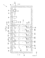
図2は、本発明の第1の実施形態におけるレーザモジュール1を模式的に示す部分断面平面図、図3は図2のA−A線断面図である。図2及び図3に示すように、このレーザモジュール1は、筐体10と、筐体10の内部に配置された階段状の台座12と、筐体10の内部に延びる光ファイバ14と、光ファイバ14を固定するためのファイバマウント16と、光ファイバ14を保持する円筒状のファイバ保持部18とを含んでいる。光ファイバ14は接着材19などによりファイバマウント16上に固定されている。なお、筐体10の上部には図示しない蓋体が配置されており、この蓋体により筐体の内部空間が封止される。
FIG. 2 is a partial cross-sectional plan view schematically showing the laser module 1 according to the first embodiment of the present invention, and FIG. 3 is a cross-sectional view taken along the line AA of FIG. As shown in FIGS. 2 and 3, the laser module 1 includes a
台座12は、Z方向の高さが異なる6つの段部12A〜12Fを有しており、本実施形態では、1段目の段部12Aから−X方向に向かって次第に高くなるように段部12A〜12Fが形成されている。それぞれの段部12A〜12Fにはサブマウント20が配置されており、それぞれのサブマウント20上には、+Y方向にレーザ光LA〜LFを出射する半導体レーザ素子22A〜22Fが載置されている。なお、本明細書では、特に言及がない場合には、半導体レーザ素子22A〜22Fのそれぞれから光ファイバ14に向かってレーザ光が出射される方向を「下流側」といい、それとは逆の方向を「上流側」ということとする。
The
また、台座12のそれぞれの段部12A〜12Fには、半導体レーザ素子22A〜22Fに対応して、半導体レーザ素子22A〜22Fから出射されたレーザ光LA〜LFをファースト軸方向にコリメートするファースト軸コリメートレンズ24と、ファースト軸コリメートレンズ24を透過したレーザ光LA〜LFをスロー軸方向にコリメートするスロー軸コリメートレンズ26と、スロー軸コリメートレンズ26を透過したレーザ光LA〜LFの伝搬方向を90度転換するミラー28とが配置されている。
Further, each stepped
また、筐体10の内部に延びる光ファイバ14の端面と台座12の1段目の段部12Aとの間には、ミラー28で反射したレーザ光LA〜LFをファースト軸方向に集光するファースト軸集光レンズ32と、レーザ光LA〜LFをスロー軸方向に集光して光ファイバ14の端面に結合させるスロー軸集光レンズ34とが配置されている。
Further, between the end surface of the
ここで、本実施形態におけるレーザモジュール1は、所定の格子間隔で屈折率が周期的に変化する波長安定化素子(VBG)41〜43を有している。これらの波長安定化素子41〜43は、特定の波長(例えば976nm)を反射するように構成されている。
Here, the laser module 1 in the present embodiment has wavelength stabilizing elements (VBG) 41 to 43 whose refractive index changes periodically at predetermined lattice intervals. These
波長安定化素子41は、台座12の1段目の段部12Aのミラー28の+X方向側に配置されており、2つのレーザ光の光路上、すなわち、1段目の段部12Aに配置された半導体レーザ素子22Aから出射されるレーザ光LA及び2段目の段部12Bに配置された半導体レーザ素子22Bから出射されるレーザ光LBの光路上に位置している。換言すれば、波長安定化素子41は、レーザ光LAの光路上及びレーザ光LBの光路上でスロー軸コリメートレンズ26及びミラー28の下流側に配置されている。
The
波長安定化素子42は、台座12の3段目の段部12Cのミラー28の+X方向側に配置されており、2つのレーザ光の光路上、すなわち、3段目の段部12Cに配置された半導体レーザ素子22Cから出射されるレーザ光LC及び4段目の段部12Dに配置された半導体レーザ素子22Dから出射されるレーザ光LDの光路上に位置している。換言すれば、波長安定化素子42は、レーザ光LCの光路上及びレーザ光LDの光路上でスロー軸コリメートレンズ26及びミラー28の下流側に配置されている。
The
波長安定化素子43は、台座12の5段目の段部12Eのミラー28の+X方向側に配置されており、2つのレーザ光の光路上、すなわち、5段目の段部12Eに配置された半導体レーザ素子22Eから出射されるレーザ光LEと6段目の段部12Fに配置された半導体レーザ素子22Fから出射されるレーザ光LFの光路上に位置している。換言すれば、波長安定化素子43は、レーザ光LEの光路上及びレーザ光LFの光路上でスロー軸コリメートレンズ26及びミラー28の下流側に配置されている。
The
このような構成において、半導体レーザ素子22Aから+Y方向に出射されたレーザ光LAは、ファースト軸コリメートレンズ24及びスロー軸コリメートレンズ26によりそれぞれファースト軸方向及びスロー軸方向にコリメートされ、ミラー28により90度方向転換されて+X方向に伝搬する。このレーザ光LAは波長安定化素子41で反射して半導体レーザ素子22Aに向かって戻り、波長安定化素子41の反射面と半導体レーザ素子22Aの活性層の反射端面との間で外部共振器が形成される。これによって、波長が狭帯域化されたレーザ光LA’が波長安定化素子41から+X方向に出力される。
In such a configuration, the
同様に、半導体レーザ素子22Bから+Y方向に出射されたレーザ光LBは、ファースト軸コリメートレンズ24及びスロー軸コリメートレンズ26を通過後、ミラー28により90度方向転換されて+X方向に伝搬し、波長安定化素子41で反射する。これにより、波長安定化素子41の反射面と半導体レーザ素子22Bの活性層の反射端面との間で外部共振器が形成され、波長が狭帯域化されたレーザ光LB’が波長安定化素子41から+X方向に出力される。
Similarly, the laser beam L B emitted from the
また、半導体レーザ素子22Cから+Y方向に出射されたレーザ光LC及び半導体レーザ素子22Dから+Y方向に出射されたレーザ光LDは、それぞれファースト軸コリメートレンズ24及びスロー軸コリメートレンズ26を通過後、ミラー28により90度方向転換されて+X方向に伝搬し、波長安定化素子42で反射して波長安定化素子42の反射面と半導体レーザ素子22C,22Dの活性層の反射端面との間で外部共振器が形成される。これにより、波長が狭帯域化されたレーザ光LC’,LD’が波長安定化素子42から+X方向に出力される。さらに、半導体レーザ素子22Eから+Y方向に出射されたレーザ光LE及び半導体レーザ素子22Fから+Y方向に出射されたレーザ光LFは、それぞれファースト軸コリメートレンズ24及びスロー軸コリメートレンズ26を通過後、ミラー28により90度方向転換されて+X方向に伝搬し、波長安定化素子43で反射して波長安定化素子43の反射面と半導体レーザ素子22E,22Fの活性層の反射端面との間で外部共振器が形成される。これにより、波長が狭帯域化されたレーザ光LE’,LF’が波長安定化素子43から+X方向に出力される。
The laser beam L D emitted in the + Y direction from the
このように、本実施形態における波長安定化素子41は、互いに異なる2つの半導体レーザ素子22A,22Bから出射されるレーザ光LA,LBの波長を狭帯域化するように構成されており、波長安定化素子42は、互いに異なる2つの半導体レーザ素子22C,22Dから出射されるレーザ光LC,LDの波長を狭帯域化するように構成されている。また、波長安定化素子43は、互いに異なる2つの半導体レーザ素子22E,22Fから出射されるレーザ光LE,LFの波長を狭帯域化するように構成されている。
Thus, the
これらの波長安定化素子41〜43で波長が狭帯域化されたレーザ光LA’〜LF’は、ファースト軸集光レンズ32によってファースト軸に集光され、さらにスロー軸集光レンズ34によってスロー軸に集光される。これによって、これらのレーザ光LA’〜LF’が光ファイバ14の端面に光学的に結合される。
These laser light wavelengths are narrowed in
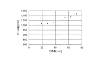
ところで、最近では、従来の図1Aに示す構成において、それぞれの半導体レーザ素子510から波長安定化素子590までの光路長が異なることにより、レーザ光B’の光ファイバ570への結合効率が低下することが分かってきている。例えば、図4は、半導体レーザ素子510と波長安定化素子590との間のレーザ光の光路長と遠方におけるスロー軸方向のビーム幅との関係を示すグラフである。図4に示すように、遠方におけるビーム幅は、半導体レーザ素子510と波長安定化素子590との間の光路長によって変化する。このように、図1Aに示す従来の構成では、波長安定化素子590とそれぞれの半導体レーザ素子510との間の光路長の差が大きいため、光ファイバ570に結合するレーザ光B’のビーム幅の変動も大きくなる。この結果、レーザ光B’の光ファイバ570への結合効率が低下してしまう。
By the way, recently, in the conventional configuration shown in FIG. 1A, the optical path length from each
これに対して、本実施形態では、6つの半導体レーザ素子22A〜22Fに対して3つの波長安定化素子41〜43を用いているため、図1Aに示す従来のレーザモジュールに比べて、波長安定化素子41〜43と半導体レーザ素子22A〜22Fとの間の光路長の差を小さくすることができる。例えば、波長安定化素子41について言えば、波長安定化素子41と半導体レーザ素子22Bとの間の光路長は、波長安定化素子41と半導体レーザ素子22Aとの間の光路長よりもd1長いだけであり、図1Aに示す従来のレーザモジュールにおける光路長の差の最大値Dmaxに比べて非常に小さい。したがって、レーザ光の光路長の差により生じ得るスロー軸方向のビーム幅の変動を小さくすることができ、この結果、光ファイバ14へのレーザ光の結合効率が低下してしまうことを抑制することができる。
On the other hand, in the present embodiment, since three
ここで、波長安定化素子と半導体レーザ素子との間の光路長の差を小さくする上では、本実施形態のように、波長安定化素子41が、互いにX方向に隣接する半導体レーザ素子22Aと半導体レーザ素子22Bとから出射されるレーザ光の波長を狭帯域化するように構成されていることが好ましい。同様に、波長安定化素子42は、互いにX方向に隣接する半導体レーザ素子22Cと半導体レーザ素子22Dとから出射されるレーザ光の波長を狭帯域化するように構成されていることが好ましく、波長安定化素子43は、互いにX方向に隣接する半導体レーザ素子22Eと半導体レーザ素子22Fとから出射されるレーザ光の波長を狭帯域化するように構成されていることが好ましい。
Here, in order to reduce the difference in the optical path length between the wavelength stabilizing element and the semiconductor laser element, as in the present embodiment, the
また、本実施形態では、複数の波長安定化素子41〜43のそれぞれが、2つの異なる半導体レーザ素子22A〜22Fから出射されるレーザ光LA〜LFの波長を狭帯域化しているため、必要とされる波長安定化素子の数を半導体レーザ素子22A〜22Fの総数の半分、すなわち3個にすることができる。したがって、本実施形態によれば、波長安定化素子の設置作業の工数が減るので、レーザモジュール1の製造コストを抑えることができる。
Further, in the present embodiment, since each of the plurality of
また、本実施形態では、波長安定化素子41〜43のそれぞれは、スロー軸コリメートレンズ26の下流側に配置されているため、それぞれの波長安定化素子41〜43によって反射されたレーザ光は、スロー軸コリメートレンズ26によってスロー軸コリメートレンズ26の焦点位置、すなわち半導体レーザ素子22A〜22Fのそれぞれの活性層に戻ることとなる。このため、半導体レーザ素子22A〜22Fの活性層外に戻るレーザ光の量が減少し、効率の良い外部共振器を形成することができる。
Further, in the present embodiment, since each of the
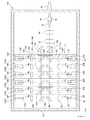
図5は、本発明の第2の実施形態におけるレーザモジュール101を模式的に示す部分断面平面図である。このレーザモジュール101は、上述した第1の実施形態における半導体レーザ素子22A〜22F(第1半導体レーザ素子)に加えて、半導体レーザ素子122A〜122F(第2半導体レーザ素子)を有している。すなわち、図5に示すように、台座12のそれぞれの段部12A〜12Fにはサブマウント120が配置されており、それぞれのサブマウント120上に、−Y方向にレーザ光MA〜MFを出射する半導体レーザ素子122A〜122Fが載置されている。
FIG. 5 is a partial cross-sectional plan view schematically showing the
半導体レーザ素子122Aは、半導体レーザ素子22Aと同一の高さで半導体レーザ素子22Aと対向するように配置され、半導体レーザ素子122Bは、半導体レーザ素子22Bと同一の高さで半導体レーザ素子22Bと対向するように配置されている。また、半導体レーザ素子122Cは、半導体レーザ素子22Cと同一の高さで半導体レーザ素子22Cと対向するように配置され、半導体レーザ素子122Dは、半導体レーザ素子22Dと同一の高さで半導体レーザ素子22Dと対向するように配置されている。さらに、半導体レーザ素子122Eは、半導体レーザ素子22Eと同一の高さで半導体レーザ素子22Eと対向するように配置され、半導体レーザ素子122Fは、半導体レーザ素子22Fと同一の高さで半導体レーザ素子22Fと対向するように配置されている。
The
また、台座12のそれぞれの段部12A〜12Fには、半導体レーザ素子122A〜122Fに対応して、半導体レーザ素子122A〜122Fから出射されたレーザ光MA〜MFをファースト軸方向にコリメートするファースト軸コリメートレンズ124と、ファースト軸コリメートレンズ124を透過したレーザ光MA〜MFをスロー軸方向にコリメートするスロー軸コリメートレンズ126と、スロー軸コリメートレンズ126を透過したレーザ光MA〜MFの伝搬方向を90度転換するミラー128とが配置されている。
Further, each stepped
また、台座12の1段目の段部12A上のミラー28とファースト軸集光レンズ32との間には、半導体レーザ素子22A〜22Fからのレーザ光と半導体レーザ素子122A〜122Fからのレーザ光とを合成してファースト軸集光レンズ32に向ける光合成部としてのビームスプリッタ150が配置されており、台座12の1段目の段部12A上のミラー128の+X方向側には、半導体レーザ素子122A〜122Fから出射されたレーザ光MA〜MFを反射してビームスプリッタ150に向ける補助ミラー152が配置されている。ビームスプリッタ150と補助ミラー152との間には1/2波長板(図示せず)が配置される。なお、上述した光合成部として、本実施形態に示すビームスプリッタ150に代えて、例えばダイクロイックミラーのような光学部品を用いることもできる。
Further, between the
本実施形態におけるレーザモジュール101は、特定の波長(例えば976nm)を反射するように構成された波長安定化素子141〜143を有している。波長安定化素子141は、台座12の1段目の段部12Aのミラー28(第1ミラー)及びミラー128(第2ミラー)の+X方向側に配置されており、Y方向に延びている。この波長安定化素子141は、4つのレーザ光の光路上、すなわち、1段目の段部12Aに配置された半導体レーザ素子22Aから出射されるレーザ光LA、この半導体レーザ素子22Aに対向する半導体レーザ素子122Aから出射されるレーザ光MA、2段目の段部12Bに配置された半導体レーザ素子22Bから出射されるレーザ光LB、この半導体レーザ素子22Bに対向する半導体レーザ素子122Bから出射されるレーザ光MBの光路上に位置している。換言すれば、波長安定化素子141は、レーザ光LAの光路上、レーザ光MAの光路上、レーザ光LBの光路上、及びレーザ光MBの光路上で対応するスロー軸コリメートレンズ26,126及び対応するミラー28,128の下流側に配置されている。
The
波長安定化素子142は、台座12の3段目の段部12Cのミラー28及びミラー128の+X方向側に配置されており、Y方向に延びている。この波長安定化素子142は、4つのレーザ光の光路上、すなわち、3段目の段部12Cに配置された半導体レーザ素子22Cから出射されるレーザ光LC、この半導体レーザ素子22Cに対向する半導体レーザ素子122Cから出射されるレーザ光MC、4段目の段部12Dに配置された半導体レーザ素子22Dから出射されるレーザ光LD、この半導体レーザ素子22Dに対向する半導体レーザ素子122Dから出射されるレーザ光MDの光路上に位置している。換言すれば、波長安定化素子142は、レーザ光LCの光路上、レーザ光MCの光路上、レーザ光LDの光路上、及びレーザ光MDの光路上で対応するスロー軸コリメートレンズ26,126及び対応するミラー28,128の下流側に配置されている。
The
波長安定化素子143は、台座12の5段目の段部12Eのミラー28及びミラー128の+X方向側に配置されており、Y方向に延びている。この波長安定化素子143は、4つのレーザ光の光路上、すなわち、5段目の段部12Eに配置された半導体レーザ素子22Eから出射されるレーザ光LE、この半導体レーザ素子22Eに対向する半導体レーザ素子122Eから出射されるレーザ光ME、6段目の段部12Fに配置された半導体レーザ素子22Fから出射されるレーザ光LF、この半導体レーザ素子22Fに対向する半導体レーザ素子122Fから出射されるレーザ光MFの光路上に位置している。換言すれば、波長安定化素子143は、レーザ光LEの光路上、レーザ光MEの光路上、レーザ光LFの光路上、及びレーザ光MFの光路上で対応するスロー軸コリメートレンズ26,126及び対応するミラー28,128の下流側に配置されている。
The
また、上述した第1の実施形態と同様に、半導体レーザ素子22A〜22Fから出射されたレーザ光LA〜LFは、それぞれファースト軸コリメートレンズ24及びスロー軸コリメートレンズ26を通過後、ミラー28により90度方向転換されて+X方向に伝搬し、波長安定化素子141〜143によって波長が狭帯域化されたレーザ光LA’〜LF’となる。
Also, as in the first embodiment described above, the semiconductor laser element laser beam L A ~L emitted from 22A-22F F after passing through the fast
半導体レーザ素子122Aから−Y方向に出射されたレーザ光MAは、ファースト軸コリメートレンズ124及びスロー軸コリメートレンズ126を通過後、ミラー128により90度方向転換されて+X方向に伝搬し、波長安定化素子141によって波長が狭帯域化されたレーザ光MA’となる。同様に、半導体レーザ素子122Bから−Y方向に出射されたレーザ光MBは、ファースト軸コリメートレンズ124及びスロー軸コリメートレンズ126を通過後、ミラー128により90度方向転換されて+X方向に伝搬し、波長安定化素子141によって波長が狭帯域化されたレーザ光MB’となる。
The
また、半導体レーザ素子122Cから−Y方向に出射されたレーザ光MC及び半導体レーザ素子122Dから−Y方向に出射されたレーザ光MDは、それぞれファースト軸コリメートレンズ124及びスロー軸コリメートレンズ126を通過後、ミラー128により90度方向転換されて+X方向に伝搬し、波長安定化素子142によって波長が狭帯域化されたレーザ光MC’,MD’となる。
The
半導体レーザ素子122Eから−Y方向に出射されたレーザ光ME及び半導体レーザ素子122Fから−Y方向に出射されたレーザ光MFは、それぞれファースト軸コリメートレンズ124及びスロー軸コリメートレンズ126を通過後、ミラー128により90度方向転換されて+X方向に伝搬し、波長安定化素子143によって波長が狭帯域化されたレーザ光ME’,MF’となる。
The semiconductor laser element laser beam M E emitted in the -Y direction from 122E and a semiconductor laser element laser beam M F emitted in the -Y direction from 122F after passing through the first
波長が狭帯域化されたレーザ光MA’〜MF’は、補助ミラー152により90度方向転換されて−Y方向に伝搬し、1/2波長板によって偏波された後、ビームスプリッタ150によってレーザ光LA’〜LF’と偏波合成されてファースト軸集光レンズ32に出力される。ファースト軸集光レンズ32でこれらのレーザ光LA’〜LF’及びMA’〜MF’はファースト軸に集光され、さらにスロー軸集光レンズ34によってスロー軸に集光される。これによって、これらのレーザ光LA’〜LF’及びMA’〜MF’が光ファイバ14の端面に光学的に結合される。
Wavelength narrowed laser beam M A '~M F' is 90 degrees diverted by the
また、本実施形態における波長安定化素子141は、互いに隣接する2つの半導体レーザ素子22A,22Bから出射されるレーザ光LA,LBと、これら2つの半導体レーザ素子22A,22Bとそれぞれ同一の高さに配置される2つの半導体レーザ素子122A,122Bから出射されるレーザ光MA,MBの波長を狭帯域化するように構成されている。また、波長安定化素子142は、互いに隣接する2つの半導体レーザ素子22C,22Dから出射されるレーザ光LC,LDと、これら2つの半導体レーザ素子22C,22Dとそれぞれ同一の高さに配置される2つの半導体レーザ素子122C,122Dから出射されるレーザ光MC,MDの波長を狭帯域化するように構成されており、波長安定化素子143は、互いに隣接する2つの半導体レーザ素子22E,22Fから出射されるレーザ光LE,LFと、これら2つの半導体レーザ素子22E,22Fとそれぞれ同一の高さに配置される2つの半導体レーザ素子122E,122Fから出射されるレーザ光ME,MFの波長を狭帯域化するように構成されている。
The
本実施形態では、12個の半導体レーザ素子22A〜22F,122A〜122Fに対して3つの波長安定化素子141〜143を用いているため、図1Aに示す従来のレーザモジュールに比べて、波長安定化素子141〜143と半導体レーザ素子22A〜22F,122A〜122Fとの間の光路長の差を小さくすることができる。したがって、レーザ光の光路長の差により生じ得るスロー軸方向のビーム幅の変動を小さくすることができ、この結果、光ファイバ14へのレーザ光の結合効率が低下してしまうことを抑制することができる。
In this embodiment, since three
また、本実施形態では、複数の波長安定化素子141〜143のそれぞれが、4つの異なる半導体レーザ素子から出射されるレーザ光の波長を狭帯域化しているため、必要とされる波長安定化素子の数を半導体レーザ素子22A〜22F,122A〜122Fの総数の1/4、すなわち3個にすることができる。したがって、本実施形態によれば、波長安定化素子の設置作業の工数が減るので、レーザモジュール101の製造コストを抑えることができる。
Further, in the present embodiment, each of the plurality of
また、本実施形態のレーザモジュール101では、半導体レーザ素子22A〜22Fから出射されるレーザ光LA’〜LF’と半導体レーザ素子122A〜122Fから出射されるレーザ光MA’〜MF’とをビームスプリッタ150により合成しているため、上述した第1の実施形態のレーザモジュール1よりも高パワーのレーザ光を出力することができる。
Further, in the
上述したレーザモジュール1又は101は、例えばファイバレーザ装置などに用いることができる。図6は、本発明に係るレーザモジュールを用いたファイバレーザ装置の一例を示す模式図である。図6に示すファイバレーザ装置401は、光共振器410と、光共振器410の前方から光共振器410に励起光を導入する複数の前方励起光源420Aと、光ファイバ421Aを介してこれらの前方励起光源420Aが接続される前方インラインコンバイナ422Aと、光共振器410の後方から光共振器410に励起光を導入する複数の後方励起光源420Bと、光ファイバ421Bを介してこれらの後方励起光源420Bが接続される後方インラインコンバイナ422Bとを備えている。上述したレーザモジュール1又は101は、前方励起光源420A及び後方励起光源420Bとして用いることができる。
The
光共振器410は、例えばイッテルビウム(Yb)やエルビウム(Er)、ツリウム(Tr)、ネオジム(Nd)などの希土類元素イオンが添加されたコアを有する増幅用光ファイバ412と、増幅用光ファイバ412及び前方インラインコンバイナ422Aと接続される高反射ファイバブラッググレーディング(高反射FBG)414と、増幅用光ファイバ412及び後方インラインコンバイナ422Bと接続される低反射ファイバブラッググレーディング(低反射FBG)416とから構成されている。例えば、増幅用光ファイバ412は、コアの周囲に形成された内側クラッドと、内側クラッドの周囲に形成された外側クラッドとを有するダブルクラッドファイバによって構成される。
The
また、ファイバレーザ装置401は、後方インラインコンバイナ422Bから延びるデリバリファイバ430をさらに有しており、このデリバリファイバ430の後流側の端部には増幅用光ファイバ412からのレーザ発振光を例えば被処理物に向けて出射するレーザ出力部460が設けられている。
Further, the
前方インラインコンバイナ422A及び後方インラインコンバイナ422Bは、それぞれ前方励起光源420A及び後方励起光源420Bから出力される励起光を結合して上述した増幅用光ファイバ412の内側クラッドに導入するものである。これにより、増幅用光ファイバ412の内側クラッドの内部を励起光が伝搬する。
The front in-
高反射FBG414は、周期的に光ファイバの屈折率を変化させて形成されるもので、所定の波長帯の光を100%に近い反射率で反射するものである。低反射FBG416は、高反射FBG414と同様に、周期的に光ファイバの屈折率を変化させて形成されるもので、高反射FBG414で反射される波長帯の光の一部を通過させ、残りを反射するものである。このように、高反射FBG414と増幅用光ファイバ412と低反射FBG416とによって、高反射FBG414と低反射FBG416との間で特定の波長帯の光を再帰的に増幅してレーザ発振を生じさせる光共振器410が構成される。
The high-reflection FBG414 is formed by periodically changing the refractive index of the optical fiber, and reflects light in a predetermined wavelength band with a reflectance close to 100%. Like the high-reflection FBG414, the low-reflection FBG416 is formed by periodically changing the refractive index of the optical fiber, and allows a part of the light in the wavelength band reflected by the high-reflection FBG414 to pass through and the rest. It is a reflection. In this way, the high-reflection FBG414, the amplification
図6に示す例では、高反射FBG414側と低反射FBG416側の双方に励起光源420A,420Bとコンバイナ422A,422Bが設けられており、双方向励起型のファイバレーザ装置となっているが、高反射FBG414側と低反射FBG416側のいずれか一方にのみ励起光源とコンバイナを設置することとしてもよい。また、光共振器410内でレーザ発振させるための反射手段としてFBGに代えてミラーを用いることもできる。
In the example shown in FIG. 6,
また、ファイバレーザ装置としては、シード光源からのシード光を励起光源からの励起光を用いて増幅するMOPAファイバレーザ装置も知られているが、上述したレーザモジュールはこのようなMOPAファイバレーザ装置の励起光源としても用いることも可能である。 Further, as a fiber laser device, a MOPA fiber laser device that amplifies seed light from a seed light source by using excitation light from an excitation light source is also known, and the above-mentioned laser module is a MOPA fiber laser device of such a MOPA fiber laser device. It can also be used as an excitation light source.
これまで本発明の好ましい実施形態について説明したが、本発明は上述の実施形態に限定されず、その技術的思想の範囲内において種々異なる形態にて実施されてよいことは言うまでもない。 Although the preferred embodiment of the present invention has been described so far, it goes without saying that the present invention is not limited to the above-described embodiment and may be implemented in various different forms within the scope of the technical idea.
1 レーザモジュール
10 筐体
12 台座
12A〜12F 段部
14 光ファイバ
20 サブマウント
22A〜22F 半導体レーザ素子(第1半導体レーザ素子)
24 ファースト軸コリメートレンズ
26 スロー軸コリメートレンズ
28 ミラー(第1ミラー)
32 ファースト軸集光レンズ
34 スロー軸集光レンズ
41〜43 波長安定化素子
101 レーザモジュール
120 サブマウント
122A〜122F 半導体レーザ素子(第2半導体レーザ素子)
124 ファースト軸コリメートレンズ
126 スロー軸コリメートレンズ
128 ミラー(第2ミラー)
141〜143 波長安定化素子
150 ビームスプリッタ(光合成部)
152 補助ミラー
401 ファイバレーザ装置
410 光共振器
412 増幅用光ファイバ
414 高反射FBG
416 低反射FBG
420A,420B 励起光源
421A,421B 光ファイバ
422A,422B インラインコンバイナ
430 デリバリファイバ
460 レーザ出力部
1
24 First
32 First-
124 First
141-143
152
416 Low reflection FBG
420A, 420B Excitation
Claims (8)
複数の半導体レーザ素子と、
前記複数の半導体レーザ素子から出射されるレーザ光を集光して前記光ファイバに結合させる集光レンズと、
前記複数の半導体レーザ素子のうち対応する半導体レーザ素子から出射されるレーザ光を反射して前記集光レンズに向ける複数のミラーと、
前記複数の半導体レーザ素子から出射されるレーザ光の波長を狭帯域化する複数の波長安定化素子と
を備え、
前記複数の波長安定化素子のそれぞれは、前記複数の半導体レーザ素子のうち互いに異なる2以上の半導体レーザ素子から出射されるレーザ光の波長を狭帯域化するように構成される、
レーザモジュール。 With optical fiber
With multiple semiconductor laser devices,
A condenser lens that collects laser light emitted from the plurality of semiconductor laser elements and couples the laser light to the optical fiber.
A plurality of mirrors that reflect the laser beam emitted from the corresponding semiconductor laser element among the plurality of semiconductor laser elements and direct them toward the condenser lens.
A plurality of wavelength stabilizing elements for narrowing the wavelength of the laser light emitted from the plurality of semiconductor laser elements are provided.
Each of the plurality of wavelength stabilizing elements is configured to narrow the wavelength of the laser light emitted from two or more different semiconductor laser elements among the plurality of semiconductor laser elements.
Laser module.
前記複数の波長安定化素子は、前記2以上の半導体レーザ素子のそれぞれから前記光ファイバに至る光路において、対応する前記コリメートレンズ及び対応する前記ミラーの下流側に配置される、
請求項1に記載のレーザモジュール。 A plurality of collimating lenses for collimating the laser light emitted from the corresponding semiconductor laser element among the plurality of semiconductor laser elements are further provided.
The plurality of wavelength stabilizing elements are arranged on the downstream side of the corresponding collimating lens and the corresponding mirror in the optical path from each of the two or more semiconductor laser elements to the optical fiber.
The laser module according to claim 1.
複数の第1半導体レーザ素子と、
前記複数の第1半導体レーザ素子に対応する複数の第2半導体レーザ素子と、
前記複数の第1半導体レーザ素子から出射されるレーザ光及び前記複数の第2半導体レーザ素子から出射されるレーザ光を集光して前記光ファイバに結合させる集光レンズと、
前記複数の第1半導体レーザ素子から出射されるレーザ光と前記複数の第2半導体レーザ素子から出射されるレーザ光とを合成して前記集光レンズに向ける光合成部と、
前記複数の第2半導体レーザ素子から出射されるレーザ光を反射して前記光合成部に向ける補助ミラーと、
前記複数の第1半導体レーザ素子のうち対応する第1半導体レーザ素子から出射されるレーザ光を反射して前記光合成部に向ける複数の第1ミラーと、
前記複数の第2半導体レーザ素子のうち対応する第2半導体レーザ素子から出射されるレーザ光を反射して前記補助ミラーに向ける複数の第2ミラーと、
前記複数の第1半導体レーザ素子及び前記複数の第2半導体レーザ素子から出射されるレーザ光の波長を狭帯域化する複数の波長安定化素子と
を備え、
前記複数の波長安定化素子のそれぞれは、前記複数の第1半導体レーザ素子のうち1以上の第1半導体レーザ素子から出射されるレーザ光と、前記複数の第2半導体レーザ素子のうち前記1以上の第1半導体レーザ素子に対応する1以上の第2半導体レーザ素子から出射されるレーザ光の波長を狭帯域化するように構成される、
レーザモジュール。 With optical fiber
With a plurality of first semiconductor laser elements,
A plurality of second semiconductor laser elements corresponding to the plurality of first semiconductor laser elements,
A condensing lens that condenses the laser light emitted from the plurality of first semiconductor laser elements and the laser light emitted from the plurality of second semiconductor laser elements and couples them to the optical fiber.
A photosynthesis unit that synthesizes the laser light emitted from the plurality of first semiconductor laser elements and the laser light emitted from the plurality of second semiconductor laser elements and directs the laser light toward the condenser lens.
An auxiliary mirror that reflects laser light emitted from the plurality of second semiconductor laser elements and directs the laser light toward the photosynthesis unit.
A plurality of first mirrors that reflect the laser light emitted from the corresponding first semiconductor laser element among the plurality of first semiconductor laser elements and direct them toward the photosynthetic unit.
A plurality of second mirrors that reflect the laser beam emitted from the corresponding second semiconductor laser element among the plurality of second semiconductor laser elements and direct them toward the auxiliary mirror.
The plurality of first semiconductor laser elements and a plurality of wavelength stabilizing elements for narrowing the wavelength of the laser light emitted from the plurality of second semiconductor laser elements are provided.
Each of the plurality of wavelength stabilizing elements includes laser light emitted from one or more of the first semiconductor laser elements of the plurality of first semiconductor laser elements, and one or more of the plurality of second semiconductor laser elements. It is configured to narrow the wavelength of the laser light emitted from one or more second semiconductor laser devices corresponding to the first semiconductor laser device of the above.
Laser module.
前記複数の第2半導体レーザ素子のうち対応する第2半導体レーザ素子から出射されるレーザ光をコリメートする複数の第2コリメートレンズと
をさらに備え、
前記複数の波長安定化素子のそれぞれは、前記1以上の第1半導体レーザ素子から前記光ファイバに至る光路において、対応する前記第1コリメートレンズ及び対応する前記第1ミラーの下流側であって、かつ、前記1以上の第2半導体レーザ素子から前記光ファイバに至る光路において、対応する前記第2コリメートレンズ及び対応する前記第2ミラーの下流側に配置される、
請求項4又は5に記載のレーザモジュール。 A plurality of first collimating lenses that collimate the laser light emitted from the corresponding first semiconductor laser element among the plurality of first semiconductor laser elements, and a plurality of first collimating lenses.
A plurality of second collimating lenses that collimate the laser light emitted from the corresponding second semiconductor laser element among the plurality of second semiconductor laser elements are further provided.
Each of the plurality of wavelength stabilizing elements is on the downstream side of the corresponding first collimating lens and the corresponding first mirror in the optical path from the one or more first semiconductor laser elements to the optical fiber. In addition, in the optical path from the one or more second semiconductor laser elements to the optical fiber, the second collimating lens and the corresponding second mirror are arranged on the downstream side.
The laser module according to claim 4 or 5.
前記1以上の第2半導体レーザ素子は、互いに隣接する2以上の第2半導体レーザ素子である、
請求項4から6のいずれか一項に記載のレーザモジュール。 The one or more first semiconductor laser elements are two or more first semiconductor laser elements adjacent to each other.
The one or more second semiconductor laser elements are two or more second semiconductor laser elements adjacent to each other.
The laser module according to any one of claims 4 to 6.
前記レーザモジュールの前記光ファイバに接続され、希土類元素イオンが添加されたコアを有する増幅用光ファイバと
を備える、ファイバレーザ装置。 An excitation light source including the laser module according to any one of claims 1 to 7.
A fiber laser apparatus comprising an optical fiber for amplification connected to the optical fiber of the laser module and having a core to which rare earth element ions are added.
Priority Applications (2)
| Application Number | Priority Date | Filing Date | Title |
|---|---|---|---|
| JP2019152464A JP2021034530A (en) | 2019-08-23 | 2019-08-23 | Laser module and fiber laser device |
| PCT/JP2020/026433 WO2021039131A1 (en) | 2019-08-23 | 2020-07-06 | Laser module and fiber laser device |
Applications Claiming Priority (1)
| Application Number | Priority Date | Filing Date | Title |
|---|---|---|---|
| JP2019152464A JP2021034530A (en) | 2019-08-23 | 2019-08-23 | Laser module and fiber laser device |
Publications (1)
| Publication Number | Publication Date |
|---|---|
| JP2021034530A true JP2021034530A (en) | 2021-03-01 |
Family
ID=74677671
Family Applications (1)
| Application Number | Title | Priority Date | Filing Date |
|---|---|---|---|
| JP2019152464A Pending JP2021034530A (en) | 2019-08-23 | 2019-08-23 | Laser module and fiber laser device |
Country Status (2)
| Country | Link |
|---|---|
| JP (1) | JP2021034530A (en) |
| WO (1) | WO2021039131A1 (en) |
Family Cites Families (9)
| Publication number | Priority date | Publication date | Assignee | Title |
|---|---|---|---|---|
| US8437086B2 (en) * | 2010-06-30 | 2013-05-07 | Jds Uniphase Corporation | Beam combining light source |
| JP2014120621A (en) * | 2012-12-17 | 2014-06-30 | Mitsubishi Electric Corp | Semiconductor laser device |
| US9214786B2 (en) * | 2013-04-09 | 2015-12-15 | Nlight Photonics Corporation | Diode laser packages with flared laser oscillator waveguides |
| US20160119063A1 (en) * | 2014-10-24 | 2016-04-28 | Lumentum Operations Llc | Wavelength locking and multiplexing of high-power semiconductor lasers |
| JP6154965B2 (en) * | 2015-06-19 | 2017-06-28 | 株式会社アマダミヤチ | Laser unit and laser device |
| WO2017026358A1 (en) * | 2015-08-07 | 2017-02-16 | カナレ電気株式会社 | Wavelength-locked beam coupling-type semiconductor laser light source |
| KR20190043021A (en) * | 2017-10-17 | 2019-04-25 | 주식회사 이오테크닉스 | Light source apparatus having high output power |
| EP3704772B1 (en) * | 2017-11-01 | 2023-05-10 | Nuburu, Inc. | Multi kw class blue laser system |
| JP6646644B2 (en) * | 2017-12-22 | 2020-02-14 | 株式会社フジクラ | Laser system |
-
2019
- 2019-08-23 JP JP2019152464A patent/JP2021034530A/en active Pending
-
2020
- 2020-07-06 WO PCT/JP2020/026433 patent/WO2021039131A1/en active Application Filing
Also Published As
| Publication number | Publication date |
|---|---|
| WO2021039131A1 (en) | 2021-03-04 |
Similar Documents
| Publication | Publication Date | Title |
|---|---|---|
| JP4226482B2 (en) | Laser beam multiplexer | |
| US6041072A (en) | Apparatus for stabilizing multiple laser sources and their application | |
| US6697192B1 (en) | High power, spectrally combined laser systems and related methods | |
| US7764723B2 (en) | High brightness laser module | |
| JPH04230085A (en) | Laser device | |
| JP2021034531A (en) | Laser module and fiber laser device | |
| US20050185885A1 (en) | Optical multiplexing method and optical multiplexer, and optical amplifier using same | |
| US7212554B2 (en) | Wavelength stabilized laser | |
| JP2013516779A (en) | High linear power laser system | |
| JP2002141607A (en) | Semiconductor laser module and optical amplifier comprising it | |
| WO2021039131A1 (en) | Laser module and fiber laser device | |
| JP4712178B2 (en) | Semiconductor laser module, laser unit, Raman amplifier, and method for suppressing Brillouin scattering and polarization degree of optical semiconductor laser module used in Raman amplifier | |
| WO2020202757A1 (en) | Laser module and fiber laser device | |
| JP7381404B2 (en) | Laser module and fiber laser equipment | |
| US9935425B2 (en) | Fiber coupled laser source pump with wavelength division multiplexer | |
| WO2020203136A1 (en) | Fiber laser device | |
| JP4899705B2 (en) | Optical amplification module | |
| JP2006073549A (en) | External resonator-type wavelength variable optical source | |
| JP2021136242A (en) | Fiber laser device | |
| JP7465149B2 (en) | Laser module and fiber laser device | |
| JP2012054349A (en) | Fiber laser oscillation device | |
| JP5084705B2 (en) | Polarization combining type semiconductor laser light source and Raman amplifier provided with the same | |
| US20230352913A1 (en) | Laser module and fiber laser device | |
| CN116565678B (en) | Laser device | |
| JP7385738B2 (en) | fiber laser equipment |