JP2020184854A - Power converter - Google Patents
Power converter Download PDFInfo
- Publication number
- JP2020184854A JP2020184854A JP2019088822A JP2019088822A JP2020184854A JP 2020184854 A JP2020184854 A JP 2020184854A JP 2019088822 A JP2019088822 A JP 2019088822A JP 2019088822 A JP2019088822 A JP 2019088822A JP 2020184854 A JP2020184854 A JP 2020184854A
- Authority
- JP
- Japan
- Prior art keywords
- terminal
- capacitor
- conductor
- terminals
- short
- Prior art date
- Legal status (The legal status is an assumption and is not a legal conclusion. Google has not performed a legal analysis and makes no representation as to the accuracy of the status listed.)
- Pending
Links
Images

Landscapes
- Inverter Devices (AREA)
Abstract
【課題】コンデンサの発熱を抑制した電力変換装置を提供する。【解決手段】電力変換装置10は、第1端子21p1と、第2端子21n1と、第1、第2端子間で直列に接続された第1、第2スイッチング素子25a1、25b1と、を含む第1パワーモジュール20−1と、第3端子21p2と、第4端子21n2と、第3、第4端子間で直列に接続された第3、第4スイッチング素子25a2、25b2と、を含む第2パワーモジュール20−2と、複数の単位コンデンサ36と、複数の単位コンデンサを相互に並列に接続する第1導体34p、33pと、第2導体34n、33nと、第1導体に接続され第1、第2端子に接続された第1コンデンサ端子と、第2導体に接続され第3、第4端子に接続された第2コンデンサ端子と、を含むコンデンサ30と、第1、第3端子間に接続された第1短絡導体22pと、第2、第4端子間に接続された第2短絡導体22nと、を備える。【選択図】図1PROBLEM TO BE SOLVED: To provide a power conversion device which suppresses heat generation of a capacitor. A power conversion device 10 includes a first terminal 21p1, a second terminal 21n1, and first and second switching elements 25a1 and 25b1 connected in series between the first and second terminals. A second power including a power module 20-1, a third terminal 21p2, a fourth terminal 21n2, and third and fourth switching elements 25a2, 25b2 connected in series between the third and fourth terminals. Module 20-2, a plurality of unit capacitors 36, first conductors 34p and 33p connecting a plurality of unit capacitors in parallel to each other, second conductors 34n and 33n, and first and first conductors connected to the first conductor. A capacitor 30 including a first capacitor terminal connected to the second terminal and a second capacitor terminal connected to the second conductor and connected to the third and fourth terminals, and connected between the first and third terminals. A first short-circuit conductor 22p and a second short-circuit conductor 22n connected between the second and fourth terminals are provided. [Selection diagram] Fig. 1
Description
本発明の実施形態は、電力変換装置に関する。 Embodiments of the present invention relate to a power converter.
直流と交流とを双方向に、あるいは一方向に変換する電力変換装置では、ブリッジ回路を含む変換器を備えたものがある。ブリッジ回路は、直流電圧を平滑するために、直流側にコンデンサを有する。電力変換器の出力容量等によっては、大容量のコンデンサが必要となり、多数のコンデンサを並列に接続することがある。 Some power converters that convert direct current and alternating current in both directions or in one direction are equipped with a converter that includes a bridge circuit. The bridge circuit has a capacitor on the DC side in order to smooth the DC voltage. Depending on the output capacity of the power converter, a large-capacity capacitor is required, and a large number of capacitors may be connected in parallel.
大きな静電容量値を実現するために、複数の単位コンデンサを並列に接続して1つのコンデンサのようにして用いることがある。また、このような並列接続された複数の単位コンデンサを単一のケースに収納したコンデンサが用いられることもある。これらのコンデンサでは、単位コンデンサを並列に接続するために、ラミネート製のブスバーや内部導体を用いて、単位コンデンサを互いに接続する構造を有していることがある。 In order to realize a large capacitance value, a plurality of unit capacitors may be connected in parallel and used as one capacitor. Further, a capacitor in which a plurality of such unit capacitors connected in parallel are housed in a single case may be used. In order to connect the unit capacitors in parallel, these capacitors may have a structure in which the unit capacitors are connected to each other by using a laminated bus bar or an internal conductor.
ブリッジ回路は、さまざまな制御方式によって制御されるが、ほとんどの制御方式で少なくとも2つの動作モードを有する。第1の動作モードは、直流−交流間で電流を入出力するモードである。この動作モードでは、異なるレグにおいて、高電位側のスイッチング素子と低電位側のスイッチング素子がスイッチング動作する。レグを切り替えることによって、電流の方向を変えることができる。第2の動作モードは、交流側にのみ電流を入出力するモードである。この動作モードでは、異なるレグにおいて、高電位側の2つのスイッチング素子がスイッチング動作し、または、低電位側のスイッチング素子がスイッチング動作する。 The bridge circuit is controlled by various control schemes, most of which have at least two modes of operation. The first operation mode is a mode in which a current is input / output between DC and AC. In this operation mode, the switching element on the high potential side and the switching element on the low potential side perform switching operations in different legs. By switching the legs, the direction of the current can be changed. The second operation mode is a mode in which current is input / output only to the AC side. In this operation mode, the two switching elements on the high potential side perform switching operations, or the switching elements on the low potential side perform switching operations in different legs.
単位コンデンサを並列接続されたコンデンサでは、第2の動作モードの期間にブスバーや内部導体に循環電流が流れる経路が発生し得る。ブスバーや内部導体に電流が流れると、これらで損失が発生し、損失によって発生した発熱が単位コンデンサに影響を及ぼすおそれがある。単位コンデンサの周囲が発熱すると、静電容量が低下したり、コンデンサの寿命が低下したりといった懸念が生じ得る。 In a capacitor in which a unit capacitor is connected in parallel, a path through which a circulating current flows through a bus bar or an internal conductor may occur during the period of the second operation mode. When a current flows through the bus bar or the internal conductor, a loss occurs in these, and the heat generated by the loss may affect the unit capacitor. When heat is generated around the unit capacitor, there may be a concern that the capacitance is reduced and the life of the capacitor is shortened.
実施形態は、コンデンサの発熱を抑制した電力変換装置を提供する。 The embodiment provides a power conversion device that suppresses heat generation of a capacitor.
実施形態に係る電力変換装置は、高電位側の第1端子と、低電位側の第2端子と、前記第1端子と前記第2端子との間で、直列に接続された第1スイッチング素子および第2スイッチング素子と、を含む第1パワーモジュールと、高電位側の第3端子と、低電位側の第4端子と、前記第3端子と前記第4端子との間で、直列に接続された第3スイッチング素子および第4スイッチング素子と、を含む第2パワーモジュールと、複数の単位コンデンサと、前記複数の単位コンデンサを高電位側で相互に並列に接続する第1導体と、前記複数の単位コンデンサを低電位側で相互に並列に接続する第2導体と、前記第1導体に接続され、前記第1端子および前記第3端子に接続された第1コンデンサ端子と、前記第2導体に接続され、前記第2端子および前記第4端子に接続された第2コンデンサ端子と、を含むコンデンサと、前記第1端子と前記第3端子との間に接続された第1短絡導体と、前記第2端子と前記第4端子との間に接続された第2短絡導体と、を備える。前記第1短絡導体の前記第1端子と前記第3端子との間のインピーダンスの大きさは、前記第1スイッチング素子および前記第3スイッチング素子に流れる循環電流および前記第1導体に流れる電流にもとづいて設定される。前記第2短絡導体の前記第2端子と前記第4端子との間のインピーダンスの大きさは、前記第2スイッチング素子および前記第4スイッチング素子に流れる循環電流および前記第2導体に流れる電流にもとづいて設定される。 The power conversion device according to the embodiment is a first switching element connected in series between the first terminal on the high potential side, the second terminal on the low potential side, and the first terminal and the second terminal. The first power module including the second switching element, the third terminal on the high potential side, the fourth terminal on the low potential side, and the third terminal and the fourth terminal are connected in series. A second power module including the third switching element and the fourth switching element, a plurality of unit capacitors, a first conductor connecting the plurality of unit capacitors in parallel with each other on the high potential side, and the plurality of units. A second conductor that connects the unit capacitors in parallel to each other on the low potential side, a first capacitor terminal that is connected to the first conductor and is connected to the first terminal and the third terminal, and the second conductor. A capacitor including a second capacitor terminal connected to the second terminal and a second capacitor terminal connected to the fourth terminal, and a first short-circuit conductor connected between the first terminal and the third terminal. A second short-circuit conductor connected between the second terminal and the fourth terminal is provided. The magnitude of the impedance between the first terminal and the third terminal of the first short-circuit conductor is based on the circulating current flowing through the first switching element and the third switching element and the current flowing through the first conductor. Is set. The magnitude of the impedance between the second terminal and the fourth terminal of the second short-circuit conductor is based on the circulating current flowing through the second switching element and the fourth switching element and the current flowing through the second conductor. Is set.
本実施形態では、コンデンサの発熱を抑制した電力変換装置が実現される。 In the present embodiment, a power conversion device that suppresses heat generation of the capacitor is realized.
以下、図面を参照しつつ、本発明の実施形態について説明する。
なお、図面は模式的または概念的なものであり、各部分の厚みと幅との関係、部分間の大きさの比率などは、必ずしも現実のものと同一とは限らない。また、同じ部分を表す場合であっても、図面により互いの寸法や比率が異なって表される場合もある。
なお、本願明細書と各図において、既出の図に関して前述したものと同様の要素には、同一の符号を付して詳細な説明を適宜省略する。
Hereinafter, embodiments of the present invention will be described with reference to the drawings.
The drawings are schematic or conceptual, and the relationship between the thickness and width of each part, the ratio of the sizes between the parts, and the like are not necessarily the same as the actual ones. Further, even when the same parts are represented, the dimensions and ratios may be different from each other depending on the drawings.
In addition, in the present specification and each figure, the same elements as those described above with respect to the above-mentioned figures are designated by the same reference numerals, and detailed description thereof will be omitted as appropriate.
(第1の実施形態)
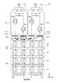
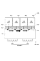
図1は、本実施形態に係る電力変換装置を例示する模式的な平面図である。
図1に示すように、本実施形態の電力変換装置10は、パワーモジュール20−1,20−2と、コンデンサ30と、短絡導体22p,22nと、を備える。
(First Embodiment)
FIG. 1 is a schematic plan view illustrating the power conversion device according to the present embodiment.
As shown in FIG. 1, the
パワーモジュール(第1パワーモジュール)20−1は、スイッチング素子(第1スイッチング素子、第2スイッチング素子)25a1,25b1を含み、同一のケース内にスイッチング素子25a1,25b1を収納している。パワーモジュール(第2パワーモジュール)20−2は、スイッチング素子(第3スイッチング素子、第4スイッチング素子)25a2,25b2を含み、同一のケース内にスイッチング素子25a2,25b2を収納している。 The power module (first power module) 20-1 includes switching elements (first switching element, second switching element) 25a1,25b1, and the switching elements 25a1,25b1 are housed in the same case. The power module (second power module) 20-2 includes switching elements (third switching element, fourth switching element) 25a2, 25b2, and the switching elements 25a2, 25b2 are housed in the same case.
パワーモジュール20−1は、端子(第1端子、第2端子)21p1,21n1を有し、パワーモジュール20−2は、端子(第3端子、第4端子)21p2,21n2を有している。スイッチング素子25a1〜25b2は、ブリッジ回路を構成している。スイッチング素子25a1〜25b2は、交流の各相に対応するレグごとにパワーモジュール20−1,20−2に収納されている。 The power module 20-1 has terminals (first terminal, second terminal) 21p1,21n1, and the power module 20-2 has terminals (third terminal, fourth terminal) 21p2,21n2. The switching elements 25a1 to 25b2 form a bridge circuit. The switching elements 25a1 to 25b2 are housed in the power modules 20-1 and 20-2 for each leg corresponding to each phase of alternating current.
コンデンサ30は、端子31p1,31n1,31p2,31n2(図2(a))を有している。パワーモジュール20−1の端子21p1,21n1は、コンデンサ30の端子(第1コンデンサ端子、第2コンデンサ端子)31p1,31n1に接続されている。パワーモジュール20−2の端子21p2,21n2は、コンデンサ30の端子(第3コンデンサ端子、第4コンデンサ端子)31p2,31n2に接続されている。つまり、パワーモジュール20−1,20−2は、端子21p1〜21n2および端子31p1〜31n2を介してコンデンサ30に電気的に接続されている。
The
短絡導体(第1短絡導体)22pは、パワーモジュール20−1の端子21p1,21p2間およびコンデンサ30の端子31p1,31p2間を、電気的に接続している。短絡導体(第2短絡導体)22nは、パワーモジュール20−2の端子21n1,21n2間およびコンデンサ30の端子31n1,31n2間を、電気的に接続している。
The short-circuit conductor (first short-circuit conductor) 22p electrically connects the terminals 21p1,21p2 of the power module 20-1 and the terminals 31p1,31p2 of the
コンデンサ30は、複数の単位コンデンサ36を含む。複数の単位コンデンサ36は、コンデンサ30の内部で導体34p,34n,33p,33nを用いて並列に接続されている。導体(第1導体)34p,33pは、端子31p1,31p2に接続されている。導体(第2導体)34n,33nは、端子31n1,31n2に接続されている。
The
以下では、インピーダンスや入力インピーダンスというときには、誘導性インピーダンスと抵抗値とのベクトル和をいうものとし、インピーダンスの大きさや入力インピーダンスの大きさは、このベクトル和の大きさ(長さ)をいうものとする。つまり、インピーダンスZは、Z=R+jωLをいうものとする。したがって、インピーダンスZの大きさ|Z|は、(R2+ω2L2)1/2である。ここで、Rは、抵抗値、Lはインダクタンス値、ωは角周波数である。RおよびLは、配線や導体等の形状等に起因する寄生的なものを含む。 In the following, when we refer to impedance and input impedance, we will refer to the vector sum of the inductive impedance and resistance value, and the magnitude of impedance and the magnitude of input impedance will refer to the magnitude (length) of this vector sum. To do. That is, the impedance Z is assumed to be Z = R + jωL. Therefore, the magnitude | Z | of the impedance Z is (R 2 + ω 2 L 2 ) 1/2 . Here, R is a resistance value, L is an inductance value, and ω is an angular frequency. R and L include parasitic substances caused by the shape of wiring, conductors, and the like.
また、以下では、スイッチング素子25a1,25a2および交流回路に電流が流れる動作を還流動作といい、スイッチング素子25b1,25b2および交流回路に電流が流れる動作も還流動作ということとする。また、還流動作によりスイッチング素子25a1,25a2および交流回路に流れる電流を循環電流といい、循環電流は、スイッチング素子25b1,25b2および交流回路の経路にも流れ得る。 Further, in the following, an operation in which a current flows through the switching elements 25a1, 25a2 and the AC circuit is referred to as a reflux operation, and an operation in which a current flows through the switching elements 25b1, 25b2 and the AC circuit is also referred to as a reflux operation. Further, the current flowing through the switching elements 25a1, 25a2 and the AC circuit by the reflux operation is called a circulating current, and the circulating current can also flow through the switching elements 25b1, 25b2 and the AC circuit path.
短絡導体22pは、端子31p1,31p2間から見た入力インピーダンスに流れる電流を分流することができるインピーダンスを有する。短絡導体22nは、端子31n1,31n2から見た入力インピーダンスに流れる電流を分流することができるインピーダンスを有する。短絡導体22pおよび短絡導体22nは、上述の端子間に接続されることによって、ブリッジ回路の高電位側のスイッチング素子25a1,25a2がスイッチング動作する場合、または低電位側のスイッチング素子25b1,25b2がスイッチング動作する場合に、コンデンサ30内に流れる電流を抑制する。
The short-
電流の流入あるいは流出が抑制されたコンデンサ30内では、導体34p,34n,33p,33nに流れる電流が抑制されるので、導体34p,34n,33p,33nの有する抵抗成分で発生する損失および発熱が低減される。
In the
短絡導体22p,22nのインピーダンスは、循環電流およびコンデンサ30内部の導体34p,34n,33p,33n等に許容される損失および発熱にもとづいて、決定される。
The impedance of the short-
たとえば、短絡導体22pは、端子31p1,31p2間から見た入力インピーダンスの大きさよりも十分小さいインピーダンスの大きさを有するように設定されている。短絡導体22nは、端子31n1,31n2間から見た入力インピーダンスの大きさよりも小さいインピーダンスを有するように設定されている。
For example, the short-
短絡導体22p,22nを用いることによって、ブリッジ回路の還流動作時に、コンデンサ30内の導体に循環電流が流れることによって生じる発熱を抑制することができる。
By using the short-
パワーモジュール20−1,20−2は、端子23−1,23−2をそれぞれ有し、電力変換装置10は、端子23−1,23−2を介して、交流回路に接続されている。この例では、交流回路は2つの相を有しており、一方がU相であり、他方がV相である。
The power modules 20-1 and 20-2 have terminals 23-1 and 23-2, respectively, and the
コンデンサ30は、端子32p,32nを有し、電力変換装置10は、端子32p,32nを介して、直流回路に接続されている。
The
電力変換装置10は、端子23−1,23−2を介して接続された交流回路と、端子32p,32nを介して接続された直流回路との間で相互に、あるいはいずれか一方向に電力変換する。
The
以下では、3次元座標を用いて説明することがある。パワーモジュール20−1,20−2およびコンデンサ30は、XY平面上に載置されているものとする。パワーモジュール20−1,20−2は、XY平面にほぼ平行な底面を有する立方体または直方体形状を有する。パワーモジュール20−1,20−2は、X軸方向に沿って配置されている。コンデンサ30は、並置されたパワーモジュール20−1,20−2の載置方向に直交するY軸方向に配置されている。
In the following, it may be described using three-dimensional coordinates. It is assumed that the power modules 20-1 and 20-2 and the
パワーモジュール20−1,20−2の端子21p1〜21n2は、XZ平面にほぼ平行なパワーモジュール20−1,20−2の側面に設けられている。端子21p1〜21n2は、パワーモジュール20−1,20−2の側面からZ軸の負方向に向かって延伸している。 The terminals 21p1 to 21n2 of the power modules 20-1 and 20-2 are provided on the side surfaces of the power modules 20-1 and 20-2 substantially parallel to the XZ plane. The terminals 21p1 to 21n2 extend from the side surfaces of the power modules 20-1 and 20-2 in the negative direction of the Z axis.
この例では、パワーモジュール20−1,20−2の端子23−1,23−2は、端子21p1〜21n2が設けられた側面に対向する側面に設けられており、Z軸の正方向に向かって延伸している。 In this example, the terminals 23-1 and 23-2 of the power modules 20-1 and 20-2 are provided on the side surface facing the side surface where the terminals 21p1 and 21n2 are provided, and face the positive direction of the Z axis. Is stretched.
コンデンサ30は、XY平面にほぼ平行な底面を有する立方体または直方体形状を有する。コンデンサ30の端子31p1〜31n2は、XZ平面にほぼ平行な側面に設けられており、Z軸の正方向に向かって延伸している。
The
この例では、コンデンサ30の端子32p,32nは、端子31p1〜31n2が設けられた側面に対向する側面に設けられており、Z軸の負方向に向かって延伸している。
In this example, the
端子21p1〜21n2および端子31p1〜31n2は、それぞれ同様の形状を有している。また、端子21p1〜21n2および端子31p1〜31n2は、十分な幅および厚さを有している。端子21p1〜21n2および端子31p1〜31n2は、X軸方向に沿って、ほぼ等間隔に配置されている。端子21p1〜21n2は、端子31p1〜31n2の位置に対応するように設けられている。 The terminals 21p1 to 21n2 and the terminals 31p1 to 31n2 have similar shapes, respectively. Further, the terminals 21p1 to 21n2 and the terminals 31p1 to 31n2 have a sufficient width and thickness. The terminals 21p1 to 21n2 and the terminals 31p1 to 31n2 are arranged at substantially equal intervals along the X-axis direction. The terminals 21p1 to 21n2 are provided so as to correspond to the positions of the terminals 31p1 to 31n2.
端子21p1,31p1は、互いに重ね合わせてネジ等で締結等され接続される。端子21n1,31n1、端子21p2,31p2、端子21n2,31n2も同様に、互いに重ね合わせてネジ等で締結等される。 The terminals 21p1 and 31p1 are overlapped with each other and fastened with screws or the like to be connected. Similarly, the terminals 21n1, 31n1, the terminals 21p2, 31p2, and the terminals 21n2, 31n2 are overlapped with each other and fastened with screws or the like.
パワーモジュール20−1,20−2およびコンデンサ30は、このような配置および端子形状とすることによって、パワーモジュール20−1,20−2とコンデンサ30との間の配線の長さを短くすることができ、配線によるインダクタンスを低減することができる。パワーモジュール20−1,20−2とコンデンサ30との間の配線によるインダクタンス値を低減することによって、不要なサージ電圧の発生や各相のパワーモジュール20−1,20−2に流れる電流の非対称性等を抑制する。
The power modules 20-1, 20-2 and the
本実施形態の電力変換装置10の動作を説明するために、コンデンサ30の構成例について詳述する。
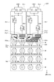
図2(a)は、本実施形態の電力変換装置の一部を例示する模式的な平面図である。図2(b)は、図2(a)のAA’線における模式的な矢視断面図である。
図2(a)および図2(b)に示すように、コンデンサ30は、複数の単位コンデンサ36と、導体33p,33n,34p,34nと、を含む。
In order to explain the operation of the
FIG. 2A is a schematic plan view illustrating a part of the power conversion device of the present embodiment. FIG. 2B is a schematic cross-sectional view taken along the line AA'of FIG. 2A.
As shown in FIGS. 2A and 2B, the
複数の単位コンデンサ36は、XY平面上で、たとえば格子状に配列されている。この例では、X軸方向に沿って4個の単位コンデンサ36が配列され、Y軸方向に沿って4個の単位コンデンサが配列されている。
The plurality of
単位コンデンサ36は、この例ではZ軸方向に沿って延伸する円柱形状の外囲器に封止されている。円柱の上下の両端に端子37p,37nが設けられている。単位コンデンサ36は、たとえば無極性のコンデンサであり、フィルムコンデンサ等である。
In this example, the
導体34pは、Y軸方向に延伸して設けられ、Y軸方向に配列された4つの単位コンデンサ36の上方の端子にそれぞれ接続されている。
The
導体34nは、導体34pとほぼ平行するように設けられ、4つの単位コンデンサ36の下方の端子にそれぞれ接続されている。
The
導体34p,34nおよび導体34p,34nによって接続された4つの単位コンデンサ36の組は、X軸方向にほぼ均等な間隔で配置されている。
The set of four
導体33pは、X軸方向に延伸して設けられ、導体34pと交差する箇所で導体34pと接続されている。導体33pは、単位コンデンサ36のY軸方向の配置に応じて4つ設けられている。
The
導体33nは、導体33pとほぼ平行に設けられ、導体34nと交差する箇所で導体34nと接続されている。導体33nは、単位コンデンサ36のY軸方向の配置に応じて4つ設けられている。
The
導体34p,33pの接続および導体34n,33nの接続は、たとえばハンダ接合や溶接等の周知の技術を用いて行われる。
The connection of the
上述のように、コンデンサ30は、導体33p〜34nを用いて互いに接続された単位コンデンサ36を含んでいる。導体33p〜34nは、有限のインピーダンスを有するので、パワーモジュール20−1,20−2や直流回路との間で電流が入出力するのにともなって、損失を生じ得る。
As described above, the
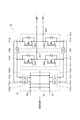
図3は、本実施形態に係る電力変換装置を例示する簡略化された回路図である。
図3では、回路素子および端子のうち図1および図2と同じものについては、同一の符号を付してある。
図3に示すように、本実施形態の電力変換装置10は、スイッチング素子25a1〜25b2からなるブリッジ回路を有している。ブリッジ回路では、スイッチング素子25a1,25b1は、直列に接続され、U相のレグを構成する。スイッチング素子25a2,25b2は、直列に接続され、V相のレグを構成する。
FIG. 3 is a simplified circuit diagram illustrating the power conversion device according to the present embodiment.
In FIG. 3, the same circuit elements and terminals as those in FIGS. 1 and 2 are designated by the same reference numerals.
As shown in FIG. 3, the
スイッチング素子25a1,25b1の直列回路は、パワーモジュール20−1に収納されている。スイッチング素子25a2,25b2の直列回路は、パワーモジュール20−2に収納されている。 The series circuit of the switching elements 25a1, 25b1 is housed in the power module 20-1. The series circuit of the switching elements 25a2 and 25b2 is housed in the power module 20-2.
スイッチング素子25a1,25b1の直列回路は、パワーモジュール20−1の端子21p1,21n1を介して、コンデンサ30に接続されている。スイッチング素子25a2,25b2の直列回路は、パワーモジュール20−2の端子21p2,21n2を介して、コンデンサ30に接続されている。
The series circuit of the switching elements 25a1,25b1 is connected to the
2つのパワーモジュール20−1,20−2の正電位側の端子21p1,21p2間および負電位側の端子21n1,21n2間には、インピーダンス素子122p,122nがそれぞれ接続されている。インピーダンス素子122pは、端子21p1,21p2間における短絡導体22pの等価的なインピーダンスを表している。インピーダンス素子122nは、端子21n1,21n2間における短絡導体22nの等価的なインピーダンスを表している。インピーダンス素子122pおよびインピーダンス素子122nは、短絡導体22p,22nのインピーダンスZ3を有する。
単位コンデンサ36と端子31p1との間には、インピーダンス素子133p1が接続されている。単位コンデンサ36と端子31p2との間には、インピーダンス素子133p2が接続されている。インピーダンス素子133p1,133p2は、コンデンサ30の端子31p1,31p2から見たときの等価的な入力インピーダンスを表している。インピーダンス素子133p1,133p2のインピーダンスは、主として、導体34p,33pの有する抵抗成分および寄生インダクタンスからなる。
An impedance element 133p1 is connected between the
単位コンデンサ36と端子31n1との間には、インピーダンス素子133n1が接続されている。単位コンデンサ36と端子31n2との間には、インピーダンス素子133n2が接続されている。インピーダンス素子133n1,133n2は、コンデンサ30の端子31n1,31n2から見たときの等価的な入力インピーダンスを表している。インピーダンス素子133n1,133n2のインピーダンスは、主として、導体34n,33nの有する抵抗成分および寄生インダクタンスからなる。
An impedance element 133n1 is connected between the
インピーダンス素子122p,122nは、これに限るものではないが、この例では、ほぼ等しいインピーダンスの大きさ|Z3|を有するものとする。インピーダンス素子133p1,133n1およびインピーダンス素子133p2,133n2は、インピーダンスZ1,Z2を有しており、端子31p1,31p2から見たインピーダンスは、Z1+Z2であり、その大きさは|Z1+Z2|と表されるものとする。
本実施形態の電力変換装置10では、それぞれのインピーダンス素子のインピーダンスの大きさ|Z1+Z2|,|Z3|は、たとえば、パワーモジュール20−1,20−2に実際に流れ得る循環電流およびコンデンサ30に流入し、またはコンデンサ30から流出する電流によって生じる発熱の許容値にもとづいて決定される。
In the
たとえば、実際に流れ得る循環電流Iaとし、インピーダンス素子133p1,133p2(または133n1,133n2)の発熱の許容値にもとづいて計算される電流Ibとすると、インピーダンス素子122p(または122n)に流れる電流Icは、以下のように求められる。
For example, assuming that the circulating current Ia that can actually flow is the current Ib that is calculated based on the heat generation allowance of the impedance elements 133p1, 133p2 (or 133n1, 133n2), the current Ic that flows through the
Ic=Ia×|Z1+Z2|/{|Z3|+|Z1+Z2|} (1) Ic = Ia × | Z1 + Z2 | / {| Z3 | + | Z1 + Z2 |} (1)
したがって、インピーダンス素子122p(または122n)のインピーダンスの大きさ|Z3|は、以下のように求められる。
Therefore, the impedance magnitude | Z3 | of the
|Z3|=Ib×|Z1+Z2|/Ic (2) | Z3 | = Ib × | Z1 + Z2 | / Ic (2)
つまり、本実施形態では、短絡導体22p,22nは、有限のインピーダンスの大きさ|Z3|を有するので、端子31p1,31p2または端子31n1,31n2に流れ込む、あるいは、流れ出す電流を分流することができる。これにより、ブリッジ回路が還流動作をしている場合に、循環電流の大部分が短絡導体22pまたは短絡導体22nを流れるので、コンデンサ30側に流れる循環電流を小さくすることができる。
That is, in the present embodiment, since the short-
式(1)および式(2)において、IaやIbは、実測され、あるいはシミュレーション等により解析的に求められるので、短絡導体22p,22nのインピーダンスの大きさは適切に設定されることができる。
In the formulas (1) and (2), Ia and Ib are actually measured or analytically obtained by simulation or the like, so that the impedance magnitudes of the short-
短絡導体22p,22nのインピーダンスの大きさ|Z3|を、端子31p1,31p2または端子31n1,31n2から見た入力インピーダンスの大きさ|Z1+Z2|よりも十分小さくすることによって、コンデンサ30側に流れる循環電流を十分に小さくすることができ、より好ましい。
By making the impedance magnitude | Z3 | of the short-
コンデンサ30に流れる電流が低減されることによって、導体33p〜34nでの発熱が低減され、コンデンサ30側の発熱を抑制することができる。
By reducing the current flowing through the
本実施形態の効果について、比較例の電力変換装置と比較しつつ説明する。
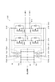
図4は、比較例の電力変換装置を例示する模式的な平面図である。
図4に示すように、比較例の電力変換装置110では、端子32p1,32p2間の短絡導体および端子32n1,32n2間の短絡導体が接続されていない点で上述の実施形態の場合と相違する。他の点では相違しない。
図5は、比較例の電力変換装置を例示する簡略化された回路図である。
図5に示すように、端子21p1,21p2間および端子21n1,21n2間に短絡導体が接続されていないことによって、これらの端子間の入力インピーダンスの大きさは理想的には無限大である。
The effect of this embodiment will be described in comparison with the power conversion device of the comparative example.
FIG. 4 is a schematic plan view illustrating a power conversion device of a comparative example.
As shown in FIG. 4, the
FIG. 5 is a simplified circuit diagram illustrating a power conversion device of a comparative example.
As shown in FIG. 5, since the short-circuit conductors are not connected between the terminals 21p1,21p2 and the terminals 21n1,21n2, the magnitude of the input impedance between these terminals is ideally infinite.
したがって、ブリッジ回路を還流する電流は、インピーダンス素子133p1,133p2(図4中の太線)または133n1,133n2に流れる。 Therefore, the current flowing back through the bridge circuit flows through the impedance elements 133p1, 133p2 (thick line in FIG. 4) or 133n1, 133n2.
ブリッジ回路は、PWM動作等するときには、高電位側のスイッチング素子および低電位側のスイッチング素子が動作するモードと、同じ電位の側のスイッチング素子が動作するモード(還流動作)と、を有している。ブリッジ回路は、動作状態に応じて、これらの動作モードを随時切り替えて動作する。 The bridge circuit has a mode in which the switching element on the high potential side and the switching element on the low potential side operate, and a mode in which the switching element on the same potential side operates (recirculation operation) when performing PWM operation or the like. There is. The bridge circuit operates by switching these operation modes at any time according to the operation state.
還流動作では、ブリッジ回路の動作原理上、コンデンサ30に電流は流入し、あるいはコンデンサ30から電流が流出することはない。しかしながら、比較例の電力変換装置110の場合には、還流動作において、パワーモジュール20−1,20−2からコンデンサ30に電流が流出入する経路が、コンデンサ30の内部の導体を介して形成される。そのため、ブリッジ回路が還流動作するときに、コンデンサ30の内部の導体に流れる電流で、導体のインピーダンスの抵抗成分による損失が発生する。
In the reflux operation, due to the operating principle of the bridge circuit, no current flows into the
たとえば、PWM制御されたブリッジ回路では、低デューティの場合に還流動作の期間が長くなることがあり、コンデンサ30の内部における損失が大きくなる傾向にある。また、電力系統用途や鉄道用途等のような大電力を扱う電力変換装置では、非常に大きな循環電流が流れることを想定して、コンデンサ30の内部の導体のインピーダンスの大きさを小さくするために、導体の幅や厚さが増大し、コンデンサ30自体が大型化するおそれもある。
For example, in a PWM-controlled bridge circuit, the period of the reflux operation may be long in the case of low duty, and the loss inside the
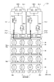
図6は、比較例の電力変換装置を例示する模式的な平面図である。
図6に示すように、比較例の電力変換装置110aでは、大電力を扱うために、パワーモジュール20−1,20−2をそれぞれを並列に接続する場合がある。端子132p,132nを介して直流回路に接続されるコンデンサ130では、内部の単位コンデンサの並列数を増やして、静電容量が増大される。
FIG. 6 is a schematic plan view illustrating a power conversion device of a comparative example.
As shown in FIG. 6, in the
このような場合に、パワーモジュール20−1,20−2をX軸方向に沿って配列し、それに応じて、コンデンサ130もX軸方向に単位コンデンサの並列を増大させることによって、相互に接続したときにインダクタンス値を低減することができる。
In such a case, the power modules 20-1 and 20-2 are arranged along the X-axis direction, and the
一方で、このように並列接続されたパワーモジュール20−1,20−2に循環電流を流すと、図示した矢印の太さで示したように、両側のパワーモジュール20−1,20−2よりも中央の中側のパワーモジュール20−1,20−2に関連する電流経路に循環電流がより集中し、コンデンサ130内の損失および発熱が大きくなる。
On the other hand, when a circulating current is passed through the power modules 20-1 and 20-2 connected in parallel in this way, as shown by the thickness of the arrow shown in the figure, the power modules 20-1 and 20-2 on both sides In addition, the circulating current is more concentrated in the current path related to the power modules 20-1 and 20-2 on the central side, and the loss and heat generation in the
これに対して、本実施形態の電力変換装置10では、パワーモジュール20−1,20−2の正側の端子21p1,21p2間および負側の端子21n1,21n2間に短絡導体22p,22nをそれぞれ接続している。短絡導体22p,22nのインピーダンスの大きさは、コンデンサ30内に流入あるいは流出する循環電流を分流して、コンデンサ30内の導体の発熱を低減するように設定されている。たとえば、短絡導体22pおよび短絡導体22nが接続されたコンデンサ30の端子31p1,31p2間および端子31n1,31n2間のそれぞれの入力インピーダンスの大きさよりも十分小さく設定されている。
On the other hand, in the
そのため、還流動作時に流れる電流は、主として短絡導体22pまたは短絡導体22nを流れ、短絡導体22p,22nのインピーダンスの大きさに応じた損失に低減される。短絡導体22p,22nは、パワーモジュール20−1,20−2およびコンデンサ30の外部に設けられるので、短絡導体22p,22nの損失による発熱は、パワーモジュール20−1,20−2およびコンデンサ30の温度上昇に直接の影響を小さくすることができる。
Therefore, the current flowing during the reflux operation mainly flows through the short-
(第2の実施形態)
図7は、本実施形態に係る電力変換装置を例示する模式的な平面図である。
図7に示すように、本実施形態の電力変換装置210では、コンデンサ230は、直流側の端子を有していない。直流側の端子は、短絡導体222p,222nに設けられている。
(Second Embodiment)
FIG. 7 is a schematic plan view illustrating the power conversion device according to the present embodiment.
As shown in FIG. 7, in the
短絡導体222pは、パワーモジュール20−1の端子21p1,21p2間およびコンデンサ30の端子31p1,31p2間を、電気的に接続するとともに、導体部分から突出する接続部を介して、直流回路に接続することができる。短絡導体222nは、パワーモジュール20−2の端子21n1,21n2間およびコンデンサ30の端子31n1,31n2間を、電気的に接続するとともに、導体部分から突出する接続部を介して、直流回路に接続することができる。
The short-
本実施形態では、短絡導体222p,222nが直流側の端子を兼ねることによって、コンデンサ230の直流側の端子を不要とすることができ、コンデンサ230の構造を簡素化することが可能になる。
In the present embodiment, since the short-
コンデンサに直流側の端子を設けたままとしてもよく、その場合には、直流側の配線や配置の自由度を高めることができる。 The DC side terminal may be left provided on the capacitor, and in that case, the degree of freedom in wiring and arrangement on the DC side can be increased.
上述の各実施形態においては、コンデンサ30は、複数の単位コンデンサ36を含むものとして説明したが、これら複数の単位コンデンサ36は、必ずしも単一のケース内に収納されてコンデンサ30を構成していなくてもよい。たとえば、図8に示すように、単一ケースに収納された単位コンデンサ236を正負の端子237p,237nを介して、ブス(第1導体、第2導体)234p,234nに接続されていてもよい。ブス234p,234nによって並列接続された複数の単位コンデンサ236を、コンデンサ230aとして取り扱うようにしてももちろんよい。
In each of the above embodiments, the
上述の他の実施形態の場合のように、正負の端子は、単位コンデンサの上下に設けられている場合に限らず、図8のように、単位コンデンサ236の一方の面に設けられていてももちろんかまわない。端子が同じ面に設けられることによって、正負のブス234p,234n間の距離を短くすることができ、ブス234p,234nによるインダクタンス値を低減することができる。正負のブス234p,234nは、たとえばラミネートブスバー等を用いることができる。
As in the case of the other embodiment described above, the positive and negative terminals are not limited to the case where they are provided above and below the unit capacitor, and even if they are provided on one surface of the
以上説明した実施形態によれば、コンデンサの発熱を抑制した電力変換装置を実現することができる。 According to the embodiment described above, it is possible to realize a power conversion device that suppresses heat generation of the capacitor.
以上、本発明のいくつかの実施形態を説明したが、これらの実施形態は、例として提示したものであり、発明の範囲を限定することは意図していない。これら新規な実施形態は、その他のさまざまな形態で実施されることが可能であり、発明の要旨を逸脱しない範囲で、種々の省略、置き換え、変更を行うことができる。これら実施形態やその変形は、発明の範囲や要旨に含まれるとともに、特許請求の範囲に記載された発明およびその等価物の範囲に含まれる。また、前述の各実施形態は、相互に組み合わせて実施することができる。 Although some embodiments of the present invention have been described above, these embodiments are presented as examples and are not intended to limit the scope of the invention. These novel embodiments can be implemented in various other embodiments, and various omissions, replacements, and changes can be made without departing from the gist of the invention. These embodiments and modifications thereof are included in the scope and gist of the invention, and are also included in the scope of the invention and its equivalents described in the claims. In addition, the above-described embodiments can be implemented in combination with each other.
10,210 電力変換装置、20−1,20−2 パワーモジュール、21p1,21n1,21p2,21n2 端子、22p,22n,222p,222n 短絡導体、25a1,25b1,25a2,25b2 スイッチング素子、30,230,230a コンデンサ、31p1,31n1,31p2,31n2 端子、33p,33n,34p,34n 導体、36,236 単位コンデンサ 10,210 Power converter, 20-1,20-2 power module, 21p1,21n1,21p2,21n2 terminal, 22p,22n,222p, 222n short-circuit conductor, 25a1,25b1,25a2,25b2 switching element, 30,230, 230a capacitor, 31p1,31n1,31p2,31n2 terminal, 33p, 33n, 34p, 34n conductor, 36,236 unit capacitor
Claims (5)
低電位側の第2端子と、
前記第1端子と前記第2端子との間で、直列に接続された第1スイッチング素子および第2スイッチング素子と、
を含む第1パワーモジュールと、
高電位側の第3端子と、
低電位側の第4端子と、
前記第3端子と前記第4端子との間で、直列に接続された第3スイッチング素子および第4スイッチング素子と、
を含む第2パワーモジュールと、
複数の単位コンデンサと、
前記複数の単位コンデンサを高電位側で相互に並列に接続する第1導体と、
前記複数の単位コンデンサを低電位側で相互に並列に接続する第2導体と、
前記第1導体に接続され、前記第1端子および前記第3端子に接続された第1コンデンサ端子と、
前記第2導体に接続され、前記第2端子および前記第4端子に接続された第2コンデンサ端子と、
を含むコンデンサと、
前記第1端子と前記第3端子との間に接続された第1短絡導体と、
前記第2端子と前記第4端子との間に接続された第2短絡導体と、
を備え、
前記第1短絡導体の前記第1端子と前記第3端子との間のインピーダンスの大きさは、前記第1スイッチング素子および前記第3スイッチング素子に流れる循環電流および前記第1導体に流れる電流にもとづいて設定され、
前記第2短絡導体の前記第2端子と前記第4端子との間のインピーダンスの大きさは、前記第2スイッチング素子および前記第4スイッチング素子に流れる循環電流および前記第2導体に流れる電流にもとづいて設定された電力変換装置。 The first terminal on the high potential side and
The second terminal on the low potential side and
A first switching element and a second switching element connected in series between the first terminal and the second terminal,
1st power module including
The third terminal on the high potential side and
The 4th terminal on the low potential side and
A third switching element and a fourth switching element connected in series between the third terminal and the fourth terminal,
2nd power module including
With multiple unit capacitors
A first conductor that connects the plurality of unit capacitors in parallel with each other on the high potential side,
A second conductor that connects the plurality of unit capacitors in parallel with each other on the low potential side,
A first capacitor terminal connected to the first conductor and connected to the first terminal and the third terminal,
A second capacitor terminal connected to the second conductor and connected to the second terminal and the fourth terminal,
With capacitors including
A first short-circuit conductor connected between the first terminal and the third terminal,
A second short-circuit conductor connected between the second terminal and the fourth terminal,
With
The magnitude of the impedance between the first terminal and the third terminal of the first short-circuit conductor is based on the circulating current flowing through the first switching element and the third switching element and the current flowing through the first conductor. Set,
The magnitude of the impedance between the second terminal and the fourth terminal of the second short-circuit conductor is based on the circulating current flowing through the second switching element and the fourth switching element and the current flowing through the second conductor. Power converter set up.
前記第1導体に接続され、前記第1端子および前記第3端子に接続された第3コンデンサ端子と、
前記第2導体に接続され、前記第2端子および前記第4端子に接続された第4コンデンサ端子と、
をさらに含み、
前記第1端子、前記第2端子、前記第3端子および前記第4端子は、第1方向に沿ってこの順に配列され、
前記第1コンデンサ端子、前記第2コンデンサ端子、前記第3コンデンサ端子および前記第4コンデンサ端子は、前記第1方向に沿ってこの順に配列されるとともに、前記第1端子、前記第2端子、前記第3端子および前記第4端子に対向する位置にそれぞれ設けられた請求項1記載の電力変換装置。 The capacitor is
A third capacitor terminal connected to the first conductor and connected to the first terminal and the third terminal,
A fourth capacitor terminal connected to the second conductor and connected to the second terminal and the fourth terminal,
Including
The first terminal, the second terminal, the third terminal, and the fourth terminal are arranged in this order along the first direction.
The first capacitor terminal, the second capacitor terminal, the third capacitor terminal, and the fourth capacitor terminal are arranged in this order along the first direction, and the first terminal, the second terminal, and the fourth capacitor terminal are arranged in this order. The power conversion device according to claim 1, which is provided at a position facing the third terminal and the fourth terminal, respectively.
前記第2短絡導体は、前記第2スイッチング素子および前記第4スイッチング素子がオンしたときに電流を流す請求項1〜3のいずれか1つの記載の電力変換装置。 The first short-circuit conductor conducts a current when the first switching element and the third switching element are turned on.
The power conversion device according to any one of claims 1 to 3, wherein the second short-circuit conductor causes a current to flow when the second switching element and the fourth switching element are turned on.
前記第2短絡導体の前記第2端子と前記第4端子との間のインピーダンスの大きさは、前記第2端子および前記第4端子から前記第2導体の側を見たインピーダンスの大きさよりも小さい請求項1〜4のいずれか1つに記載の電力変換装置。 The magnitude of the impedance between the first terminal and the third terminal of the first short-circuit conductor is smaller than the magnitude of the impedance when the side of the first conductor is viewed from the first terminal and the third terminal. ,
The magnitude of the impedance between the second terminal and the fourth terminal of the second short-circuit conductor is smaller than the magnitude of the impedance when the side of the second conductor is viewed from the second terminal and the fourth terminal. The power conversion device according to any one of claims 1 to 4.
Priority Applications (1)
| Application Number | Priority Date | Filing Date | Title |
|---|---|---|---|
| JP2019088822A JP2020184854A (en) | 2019-05-09 | 2019-05-09 | Power converter |
Applications Claiming Priority (1)
| Application Number | Priority Date | Filing Date | Title |
|---|---|---|---|
| JP2019088822A JP2020184854A (en) | 2019-05-09 | 2019-05-09 | Power converter |
Publications (1)
| Publication Number | Publication Date |
|---|---|
| JP2020184854A true JP2020184854A (en) | 2020-11-12 |
Family
ID=73045574
Family Applications (1)
| Application Number | Title | Priority Date | Filing Date |
|---|---|---|---|
| JP2019088822A Pending JP2020184854A (en) | 2019-05-09 | 2019-05-09 | Power converter |
Country Status (1)
| Country | Link |
|---|---|
| JP (1) | JP2020184854A (en) |
Citations (5)
| Publication number | Priority date | Publication date | Assignee | Title |
|---|---|---|---|---|
| JP2001258267A (en) * | 2000-03-14 | 2001-09-21 | Mitsubishi Electric Corp | Semiconductor device |
| JP2006101685A (en) * | 2004-08-31 | 2006-04-13 | Matsushita Electric Ind Co Ltd | Inverter device |
| JP2010074994A (en) * | 2008-09-19 | 2010-04-02 | Toshiba Mitsubishi-Electric Industrial System Corp | Semiconductor power converter |
| JP2013074712A (en) * | 2011-09-28 | 2013-04-22 | Mitsuba Corp | Sr motor control apparatus |
| JP2016058688A (en) * | 2014-09-12 | 2016-04-21 | 株式会社豊田自動織機 | Capacitor module, and method of manufacturing capacitor module |
-
2019
- 2019-05-09 JP JP2019088822A patent/JP2020184854A/en active Pending
Patent Citations (5)
| Publication number | Priority date | Publication date | Assignee | Title |
|---|---|---|---|---|
| JP2001258267A (en) * | 2000-03-14 | 2001-09-21 | Mitsubishi Electric Corp | Semiconductor device |
| JP2006101685A (en) * | 2004-08-31 | 2006-04-13 | Matsushita Electric Ind Co Ltd | Inverter device |
| JP2010074994A (en) * | 2008-09-19 | 2010-04-02 | Toshiba Mitsubishi-Electric Industrial System Corp | Semiconductor power converter |
| JP2013074712A (en) * | 2011-09-28 | 2013-04-22 | Mitsuba Corp | Sr motor control apparatus |
| JP2016058688A (en) * | 2014-09-12 | 2016-04-21 | 株式会社豊田自動織機 | Capacitor module, and method of manufacturing capacitor module |
Similar Documents
| Publication | Publication Date | Title |
|---|---|---|
| CN107425737B (en) | Power modules, converters and wind turbines | |
| JP6707190B2 (en) | Power conversion unit | |
| CN105794326B (en) | Power battery with printed circuit board | |
| JP5052705B2 (en) | Switching power supply | |
| WO2014024320A1 (en) | Power module comprising two elements, and three-level power conversion device using same | |
| JP2021078233A (en) | Electric power conversion system | |
| JP7035845B2 (en) | Power converter | |
| JP2015139299A (en) | power converter | |
| CN106716808B (en) | Low inductance circuit device for inverter | |
| JP2015139270A (en) | Power converter | |
| JPWO2013051475A1 (en) | Power converter | |
| JP2015035862A (en) | Power conversion device | |
| JP2019033670A (en) | Power conversion device | |
| JP2018133864A (en) | Output side connection structure of single-phase inverter | |
| JP6969502B2 (en) | Power converter | |
| JP2006333590A (en) | AC-AC power converter | |
| JP2014042377A (en) | Power supply bus bar and power converter using the same | |
| JP2020184854A (en) | Power converter | |
| JP4957842B2 (en) | Power converter | |
| JP6178178B2 (en) | Noise filter | |
| JP5913177B2 (en) | Power circuit | |
| JP6693484B2 (en) | Power converter | |
| JP6693349B2 (en) | Power converter | |
| JP6851242B2 (en) | Power converter | |
| JP6950804B2 (en) | Output side connection structure of single-phase inverter |
Legal Events
| Date | Code | Title | Description |
|---|---|---|---|
| A621 | Written request for application examination |
Free format text: JAPANESE INTERMEDIATE CODE: A621 Effective date: 20210623 |
|
| A977 | Report on retrieval |
Free format text: JAPANESE INTERMEDIATE CODE: A971007 Effective date: 20220509 |
|
| A131 | Notification of reasons for refusal |
Free format text: JAPANESE INTERMEDIATE CODE: A131 Effective date: 20220511 |
|
| A521 | Request for written amendment filed |
Free format text: JAPANESE INTERMEDIATE CODE: A523 Effective date: 20220706 |
|
| A131 | Notification of reasons for refusal |
Free format text: JAPANESE INTERMEDIATE CODE: A131 Effective date: 20221111 |
|
| A02 | Decision of refusal |
Free format text: JAPANESE INTERMEDIATE CODE: A02 Effective date: 20230508 |