JP2020106845A - Flexible wiring body, drive system and imaging apparatus - Google Patents
Flexible wiring body, drive system and imaging apparatus Download PDFInfo
- Publication number
- JP2020106845A JP2020106845A JP2020021006A JP2020021006A JP2020106845A JP 2020106845 A JP2020106845 A JP 2020106845A JP 2020021006 A JP2020021006 A JP 2020021006A JP 2020021006 A JP2020021006 A JP 2020021006A JP 2020106845 A JP2020106845 A JP 2020106845A
- Authority
- JP
- Japan
- Prior art keywords
- movable
- actuator
- flexible wiring
- semiconductor element
- wiring body
- Prior art date
- Legal status (The legal status is an assumption and is not a legal conclusion. Google has not performed a legal analysis and makes no representation as to the accuracy of the status listed.)
- Pending
Links
- 238000003384 imaging method Methods 0.000 title claims description 8
- 239000004065 semiconductor Substances 0.000 claims abstract description 63
- 238000013519 translation Methods 0.000 claims abstract description 20
- 239000000758 substrate Substances 0.000 claims description 24
- 239000011347 resin Substances 0.000 claims description 19
- 229920005989 resin Polymers 0.000 claims description 19
- 238000006073 displacement reaction Methods 0.000 claims description 13
- 239000006247 magnetic powder Substances 0.000 claims description 10
- 238000005452 bending Methods 0.000 claims description 6
- 230000005489 elastic deformation Effects 0.000 claims description 6
- 230000006641 stabilisation Effects 0.000 claims description 4
- 238000011105 stabilization Methods 0.000 claims description 4
- 239000011230 binding agent Substances 0.000 claims description 3
- 238000000034 method Methods 0.000 abstract description 13
- 238000004891 communication Methods 0.000 abstract description 11
- 230000008569 process Effects 0.000 abstract description 6
- 238000004519 manufacturing process Methods 0.000 abstract description 4
- 230000014616 translation Effects 0.000 abstract 1
- 239000010410 layer Substances 0.000 description 67
- 244000126211 Hericium coralloides Species 0.000 description 32
- 238000012986 modification Methods 0.000 description 20
- 230000004048 modification Effects 0.000 description 20
- 239000012790 adhesive layer Substances 0.000 description 16
- 239000000463 material Substances 0.000 description 7
- 230000007246 mechanism Effects 0.000 description 7
- RYGMFSIKBFXOCR-UHFFFAOYSA-N Copper Chemical compound [Cu] RYGMFSIKBFXOCR-UHFFFAOYSA-N 0.000 description 4
- 229910052581 Si3N4 Inorganic materials 0.000 description 4
- 239000010949 copper Substances 0.000 description 4
- 238000011161 development Methods 0.000 description 4
- 238000000605 extraction Methods 0.000 description 4
- HQVNEWCFYHHQES-UHFFFAOYSA-N silicon nitride Chemical compound N12[Si]34N5[Si]62N3[Si]51N64 HQVNEWCFYHHQES-UHFFFAOYSA-N 0.000 description 4
- 229910052802 copper Inorganic materials 0.000 description 3
- 239000010408 film Substances 0.000 description 3
- 239000002356 single layer Substances 0.000 description 3
- 239000004642 Polyimide Substances 0.000 description 2
- 238000005516 engineering process Methods 0.000 description 2
- 238000002955 isolation Methods 0.000 description 2
- 238000007747 plating Methods 0.000 description 2
- 229920001721 polyimide Polymers 0.000 description 2
- 238000012545 processing Methods 0.000 description 2
- 239000010409 thin film Substances 0.000 description 2
- 229910018072 Al 2 O 3 Inorganic materials 0.000 description 1
- 229910018979 CoPt Inorganic materials 0.000 description 1
- XUIMIQQOPSSXEZ-UHFFFAOYSA-N Silicon Chemical compound [Si] XUIMIQQOPSSXEZ-UHFFFAOYSA-N 0.000 description 1
- 239000000654 additive Substances 0.000 description 1
- 230000000996 additive effect Effects 0.000 description 1
- 239000000853 adhesive Substances 0.000 description 1
- 230000001070 adhesive effect Effects 0.000 description 1
- PNEYBMLMFCGWSK-UHFFFAOYSA-N aluminium oxide Inorganic materials [O-2].[O-2].[O-2].[Al+3].[Al+3] PNEYBMLMFCGWSK-UHFFFAOYSA-N 0.000 description 1
- 230000000712 assembly Effects 0.000 description 1
- 238000000429 assembly Methods 0.000 description 1
- 230000015572 biosynthetic process Effects 0.000 description 1
- 239000000919 ceramic Substances 0.000 description 1
- 238000006243 chemical reaction Methods 0.000 description 1
- 239000011889 copper foil Substances 0.000 description 1
- 239000013078 crystal Substances 0.000 description 1
- 230000000694 effects Effects 0.000 description 1
- 238000005530 etching Methods 0.000 description 1
- 239000011521 glass Substances 0.000 description 1
- 230000006872 improvement Effects 0.000 description 1
- 238000004518 low pressure chemical vapour deposition Methods 0.000 description 1
- 239000000696 magnetic material Substances 0.000 description 1
- 229910052751 metal Inorganic materials 0.000 description 1
- 239000002184 metal Substances 0.000 description 1
- 229910001172 neodymium magnet Inorganic materials 0.000 description 1
- 238000005498 polishing Methods 0.000 description 1
- 229910021420 polycrystalline silicon Inorganic materials 0.000 description 1
- 229920005591 polysilicon Polymers 0.000 description 1
- 238000003825 pressing Methods 0.000 description 1
- 230000001681 protective effect Effects 0.000 description 1
- 230000009467 reduction Effects 0.000 description 1
- 230000011514 reflex Effects 0.000 description 1
- 229910052710 silicon Inorganic materials 0.000 description 1
- 239000010703 silicon Substances 0.000 description 1
Images


Classifications
-
- H—ELECTRICITY
- H01—ELECTRIC ELEMENTS
- H01L—SEMICONDUCTOR DEVICES NOT COVERED BY CLASS H10
- H01L23/00—Details of semiconductor or other solid state devices
- H01L23/48—Arrangements for conducting electric current to or from the solid state body in operation, e.g. leads, terminal arrangements ; Selection of materials therefor
- H01L23/488—Arrangements for conducting electric current to or from the solid state body in operation, e.g. leads, terminal arrangements ; Selection of materials therefor consisting of soldered or bonded constructions
- H01L23/498—Leads, i.e. metallisations or lead-frames on insulating substrates, e.g. chip carriers
- H01L23/49838—Geometry or layout
-
- H—ELECTRICITY
- H05—ELECTRIC TECHNIQUES NOT OTHERWISE PROVIDED FOR
- H05K—PRINTED CIRCUITS; CASINGS OR CONSTRUCTIONAL DETAILS OF ELECTRIC APPARATUS; MANUFACTURE OF ASSEMBLAGES OF ELECTRICAL COMPONENTS
- H05K1/00—Printed circuits
- H05K1/02—Details
- H05K1/0277—Bendability or stretchability details
- H05K1/028—Bending or folding regions of flexible printed circuits
-
- G—PHYSICS
- G03—PHOTOGRAPHY; CINEMATOGRAPHY; ANALOGOUS TECHNIQUES USING WAVES OTHER THAN OPTICAL WAVES; ELECTROGRAPHY; HOLOGRAPHY
- G03B—APPARATUS OR ARRANGEMENTS FOR TAKING PHOTOGRAPHS OR FOR PROJECTING OR VIEWING THEM; APPARATUS OR ARRANGEMENTS EMPLOYING ANALOGOUS TECHNIQUES USING WAVES OTHER THAN OPTICAL WAVES; ACCESSORIES THEREFOR
- G03B5/00—Adjustment of optical system relative to image or object surface other than for focusing
-
- H—ELECTRICITY
- H02—GENERATION; CONVERSION OR DISTRIBUTION OF ELECTRIC POWER
- H02K—DYNAMO-ELECTRIC MACHINES
- H02K41/00—Propulsion systems in which a rigid body is moved along a path due to dynamo-electric interaction between the body and a magnetic field travelling along the path
- H02K41/02—Linear motors; Sectional motors
- H02K41/035—DC motors; Unipolar motors
- H02K41/0352—Unipolar motors
- H02K41/0354—Lorentz force motors, e.g. voice coil motors
-
- H—ELECTRICITY
- H02—GENERATION; CONVERSION OR DISTRIBUTION OF ELECTRIC POWER
- H02N—ELECTRIC MACHINES NOT OTHERWISE PROVIDED FOR
- H02N1/00—Electrostatic generators or motors using a solid moving electrostatic charge carrier
- H02N1/002—Electrostatic motors
- H02N1/006—Electrostatic motors of the gap-closing type
-
- H—ELECTRICITY
- H04—ELECTRIC COMMUNICATION TECHNIQUE
- H04M—TELEPHONIC COMMUNICATION
- H04M1/00—Substation equipment, e.g. for use by subscribers
- H04M1/02—Constructional features of telephone sets
- H04M1/0202—Portable telephone sets, e.g. cordless phones, mobile phones or bar type handsets
- H04M1/026—Details of the structure or mounting of specific components
- H04M1/0264—Details of the structure or mounting of specific components for a camera module assembly
-
- H—ELECTRICITY
- H05—ELECTRIC TECHNIQUES NOT OTHERWISE PROVIDED FOR
- H05K—PRINTED CIRCUITS; CASINGS OR CONSTRUCTIONAL DETAILS OF ELECTRIC APPARATUS; MANUFACTURE OF ASSEMBLAGES OF ELECTRICAL COMPONENTS
- H05K1/00—Printed circuits
- H05K1/02—Details
- H05K1/0213—Electrical arrangements not otherwise provided for
- H05K1/0237—High frequency adaptations
-
- H—ELECTRICITY
- H01—ELECTRIC ELEMENTS
- H01L—SEMICONDUCTOR DEVICES NOT COVERED BY CLASS H10
- H01L23/00—Details of semiconductor or other solid state devices
- H01L23/48—Arrangements for conducting electric current to or from the solid state body in operation, e.g. leads, terminal arrangements ; Selection of materials therefor
- H01L23/488—Arrangements for conducting electric current to or from the solid state body in operation, e.g. leads, terminal arrangements ; Selection of materials therefor consisting of soldered or bonded constructions
- H01L23/498—Leads, i.e. metallisations or lead-frames on insulating substrates, e.g. chip carriers
- H01L23/4985—Flexible insulating substrates
-
- H—ELECTRICITY
- H01—ELECTRIC ELEMENTS
- H01L—SEMICONDUCTOR DEVICES NOT COVERED BY CLASS H10
- H01L27/00—Devices consisting of a plurality of semiconductor or other solid-state components formed in or on a common substrate
- H01L27/14—Devices consisting of a plurality of semiconductor or other solid-state components formed in or on a common substrate including semiconductor components sensitive to infrared radiation, light, electromagnetic radiation of shorter wavelength or corpuscular radiation and specially adapted either for the conversion of the energy of such radiation into electrical energy or for the control of electrical energy by such radiation
- H01L27/144—Devices controlled by radiation
- H01L27/146—Imager structures
- H01L27/14601—Structural or functional details thereof
- H01L27/14618—Containers
-
- H—ELECTRICITY
- H04—ELECTRIC COMMUNICATION TECHNIQUE
- H04M—TELEPHONIC COMMUNICATION
- H04M2250/00—Details of telephonic subscriber devices
- H04M2250/52—Details of telephonic subscriber devices including functional features of a camera
-
- H—ELECTRICITY
- H04—ELECTRIC COMMUNICATION TECHNIQUE
- H04N—PICTORIAL COMMUNICATION, e.g. TELEVISION
- H04N23/00—Cameras or camera modules comprising electronic image sensors; Control thereof
- H04N23/50—Constructional details
- H04N23/54—Mounting of pick-up tubes, electronic image sensors, deviation or focusing coils
-
- H—ELECTRICITY
- H04—ELECTRIC COMMUNICATION TECHNIQUE
- H04N—PICTORIAL COMMUNICATION, e.g. TELEVISION
- H04N23/00—Cameras or camera modules comprising electronic image sensors; Control thereof
- H04N23/57—Mechanical or electrical details of cameras or camera modules specially adapted for being embedded in other devices
-
- H—ELECTRICITY
- H04—ELECTRIC COMMUNICATION TECHNIQUE
- H04N—PICTORIAL COMMUNICATION, e.g. TELEVISION
- H04N23/00—Cameras or camera modules comprising electronic image sensors; Control thereof
- H04N23/60—Control of cameras or camera modules
- H04N23/68—Control of cameras or camera modules for stable pick-up of the scene, e.g. compensating for camera body vibrations
- H04N23/682—Vibration or motion blur correction
- H04N23/685—Vibration or motion blur correction performed by mechanical compensation
- H04N23/687—Vibration or motion blur correction performed by mechanical compensation by shifting the lens or sensor position
-
- H—ELECTRICITY
- H05—ELECTRIC TECHNIQUES NOT OTHERWISE PROVIDED FOR
- H05K—PRINTED CIRCUITS; CASINGS OR CONSTRUCTIONAL DETAILS OF ELECTRIC APPARATUS; MANUFACTURE OF ASSEMBLAGES OF ELECTRICAL COMPONENTS
- H05K1/00—Printed circuits
- H05K1/18—Printed circuits structurally associated with non-printed electric components
- H05K1/189—Printed circuits structurally associated with non-printed electric components characterised by the use of a flexible or folded printed circuit
-
- H—ELECTRICITY
- H05—ELECTRIC TECHNIQUES NOT OTHERWISE PROVIDED FOR
- H05K—PRINTED CIRCUITS; CASINGS OR CONSTRUCTIONAL DETAILS OF ELECTRIC APPARATUS; MANUFACTURE OF ASSEMBLAGES OF ELECTRICAL COMPONENTS
- H05K2201/00—Indexing scheme relating to printed circuits covered by H05K1/00
- H05K2201/05—Flexible printed circuits [FPCs]
- H05K2201/052—Branched
-
- H—ELECTRICITY
- H05—ELECTRIC TECHNIQUES NOT OTHERWISE PROVIDED FOR
- H05K—PRINTED CIRCUITS; CASINGS OR CONSTRUCTIONAL DETAILS OF ELECTRIC APPARATUS; MANUFACTURE OF ASSEMBLAGES OF ELECTRICAL COMPONENTS
- H05K2201/00—Indexing scheme relating to printed circuits covered by H05K1/00
- H05K2201/10—Details of components or other objects attached to or integrated in a printed circuit board
- H05K2201/10007—Types of components
- H05K2201/10121—Optical component, e.g. opto-electronic component
-
- H—ELECTRICITY
- H05—ELECTRIC TECHNIQUES NOT OTHERWISE PROVIDED FOR
- H05K—PRINTED CIRCUITS; CASINGS OR CONSTRUCTIONAL DETAILS OF ELECTRIC APPARATUS; MANUFACTURE OF ASSEMBLAGES OF ELECTRICAL COMPONENTS
- H05K2201/00—Indexing scheme relating to printed circuits covered by H05K1/00
- H05K2201/10—Details of components or other objects attached to or integrated in a printed circuit board
- H05K2201/10007—Types of components
- H05K2201/10151—Sensor
Abstract
Description
本発明は、フレキシブル配線体、駆動システムおよび撮像装置に関する。 The present invention relates to a flexible wiring body, a drive system, and an imaging device.
スマートフォン等のカメラには、機械的な手振れ補正(OIS:Optical Image Stabilization)機能、および機械的な焦点合わせ機能を有するものがある。これは、レンズをボイスコイルモータ(VCM)で並進させることによって実現されている。 Some cameras such as smartphones have a mechanical image stabilization (OIS) function and a mechanical focusing function. This is achieved by translating the lens with a voice coil motor (VCM).
一方、レンズを動かさずに撮像素子(CMOSイメージャ等)を動かすOISシステムもある。レンズは軸周りに回転させても効果はないが、撮像素子を動かすことで回転方向の手ぶれを補正できることが,このOISシステムの特長である。このようなOISシステムは、スマートフォンには大き過ぎ、高価であるため、一眼レフでのみ採用されている。 On the other hand, there is also an OIS system that moves an image sensor (CMOS imager or the like) without moving the lens. Rotating the lens around the axis has no effect, but the feature of this OIS system is that it can correct camera shake in the rotation direction by moving the image sensor. Since such an OIS system is too large and expensive for smartphones, it is used only in single-lens reflex cameras.
しかし近年、撮像素子移動型のOISシステムをスマートフォンに採用したいという要望が高まっている。これをスマートフォンに搭載するためには,OISシステムを十分小型に、しかも安価に作製する必要があることから、MEMS(Micro Electro Mechanical Systems)技術の利用が検討されている。 However, in recent years, there is an increasing demand for adopting a mobile image sensor OIS system in a smartphone. In order to mount this on a smartphone, it is necessary to make the OIS system small enough and at low cost, and thus the use of MEMS (Micro Electro Mechanical Systems) technology is being studied.
MEMS技術を用いて、並進かつ回転するアクチュエータを、撮像素子と同程度のフットプリントで実現することはできるが、数十μm以上の大きな変位を、しかも多軸で発生させるように設計すると、アクチュエータの発生力が小さくなる。一方、撮像素子からは数十本もの配線を外部に取り出さなくてはならず、しかもその配線の一部は高速通信を行う高周波配線であり、また他の一部は消費電力の大きい撮像素子に電流を供給するための電源配線である。撮像素子を動かすには、このような配線を一緒に(引きずって)動かさなくてはならず、その抵抗は小型アクチュエータにとって大きな負荷になる。したがって、撮像素子移動型の小型OISシステムを実現するためには、アクチュエータの発生力を高めるとともに、撮像素子からどのように配線を取り出すかが鍵の1つになる。 Although it is possible to realize an actuator that translates and rotates using a MEMS technology with a footprint comparable to that of an image pickup element, if the actuator is designed to generate a large displacement of several tens of μm or more and also in multiple axes, The power to generate is reduced. On the other hand, dozens of wires must be taken out from the image sensor, and part of the wire is a high-frequency wire that performs high-speed communication, and the other part is an image sensor with high power consumption. It is a power supply wiring for supplying an electric current. In order to move the image pickup device, it is necessary to move (squeeze) such wirings together, and its resistance becomes a large load on the small actuator. Therefore, in order to realize a compact OIS system of a moving image pickup device, one of the keys is to increase the generated force of the actuator and how to take out the wiring from the image pickup device.
従来、3軸運動するように構成されたMEMSアクチュエータを備える多軸MEMSアセンブリがある。例えば、一端がMEMSアクチュエータコアに、他端が外側フレームに取り付けられた導電性屈曲部を有し、該導電性屈曲部が電気信号をMEMSアクチュエータコアの光電変換素子から外側フレームに供給するMEMSアクチュエータが開示されている(特許文献1)。また、周囲から外側フレームを押圧し、外側フレームを構成するバー同士をラッチ構造で固定することで、外側フレームと内側フレームに接続されたU字形の薄膜配線を上に立ち上げる構造を有するMEMSアクチュエータが開示されている(特許文献2)。このMEMSアクチュエータでは、撮像素子の移動に伴ってU字形薄膜配線が倒れたり起き上がったりするように変形し、これにより多数の配線の機械的負荷(機械的抵抗)が小さくなるとされている。 Conventionally, there are multi-axis MEMS assemblies that include a MEMS actuator configured to move in three axes. For example, a MEMS actuator having a conductive bending portion attached to the MEMS actuator core at one end and an outer frame at the other end, and the conductive bending portion supplies an electric signal from a photoelectric conversion element of the MEMS actuator core to the outer frame. Is disclosed (Patent Document 1). Further, a MEMS actuator having a structure in which a U-shaped thin film wiring connected to the outer frame and the inner frame is raised by pressing the outer frame from the surroundings and fixing the bars forming the outer frame with a latch structure. Is disclosed (Patent Document 2). In this MEMS actuator, it is said that the U-shaped thin film wiring is deformed so as to fall or rise with the movement of the image pickup element, thereby reducing the mechanical load (mechanical resistance) of many wirings.
しかしながら、上記特許文献1の技術では、導電性屈曲部が高速通信用の高周波信号と撮像素子駆動用の大電流の双方を流せるか否かについての開示は無く、改善の余地がある。また、上記特許文献2の技術では、外側フレームの構造が複雑であると共にMEMSアクチュエータの組立工程が煩雑であり、また、MEMSアクチュエータに取り付けられる撮像素子の位置決め性能が懸念される。 However, the technique of Patent Document 1 does not disclose whether or not the conductive bent portion can pass both a high-frequency signal for high-speed communication and a large current for driving the image sensor, and there is room for improvement. Further, in the technique of Patent Document 2, the structure of the outer frame is complicated, the assembly process of the MEMS actuator is complicated, and the positioning performance of the image pickup device attached to the MEMS actuator is concerned.
本発明の目的は、高速通信用の高周波信号と撮像素子駆動用の大電流の双方を安定的に流すことができると共に、アクチュエータに取り付けられる撮像素子の位置決め性能を向上することができ、更には煩雑な組立工程が不要で大量生産にも対応可能なフレキシブル配線体、駆動システムおよび撮像装置を提供することにある。 An object of the present invention is to allow both a high-frequency signal for high-speed communication and a large current for driving an image sensor to flow stably, and improve the positioning performance of an image sensor attached to an actuator. It is an object of the present invention to provide a flexible wiring body, a drive system, and an image pickup device that do not require a complicated assembling process and can be adapted to mass production.
上記目的を達成するべく、本発明は、以下の手段を提供する。
[1]互いに直交する3方向の並進及び前記3方向の軸回りの回転のうちの少なくとも1つの動きをするアクチュエータに伴って移動する半導体素子と、該半導体素子の外方に位置する枠体とを接続するフレキシブル配線体であって、
前記半導体素子が載置され、前記半導体素子と電気的に接続される主部と、
前記主部から前記枠体に向かって延出し、三次元的に曲げられた複数の腕部と、
を有する、フレキシブル配線体。
In order to achieve the above object, the present invention provides the following means.
[1] A semiconductor element that moves with an actuator that performs at least one of translation in three directions orthogonal to each other and rotation about an axis in the three directions, and a frame body located outside the semiconductor element. A flexible wiring body for connecting
A main portion on which the semiconductor element is placed and electrically connected to the semiconductor element,
Extending from the main portion toward the frame, a plurality of three-dimensionally bent arm portion,
And a flexible wiring body.
[2]前記腕部は、前記主部の主面と交わる主面を有するように曲げられ、更に折り返して曲げられており、
前記腕部の変形によって前記半導体素子の横方向、縦方向及び前記半導体素子の主面に対して垂直な方向の軸回りの回転に自由度を与える、上記[1]に記載のフレキシブル配線体。
[2] The arm portion is bent so as to have a main surface that intersects with the main surface of the main portion, and is further folded back and bent,
The flexible wiring body according to the above [1], wherein the deformation of the arm portion gives a degree of freedom to rotation of the semiconductor element in a lateral direction, a longitudinal direction, and a rotation about an axis in a direction perpendicular to a main surface of the semiconductor element.
[3]前記複数の腕部は、4つ以上である、上記[1]又は[2]に記載のフレキシブル配線体。 [3] The flexible wiring body according to the above [1] or [2], wherein the plurality of arm portions is four or more.
[4]前記主部の平面視において、前記複数の腕部が前記主部を基準として対称に配置され、
前記複数の腕部が折り返して曲げられていることによって弾性変形による力が釣り合った状態が維持されている、上記[1]〜[3]のいずれかに記載のフレキシブル配線体。
[4] In a plan view of the main portion, the plurality of arm portions are arranged symmetrically with respect to the main portion,
The flexible wiring body according to any one of the above [1] to [3], wherein the plurality of arm portions are folded back and bent to maintain a state where the forces due to elastic deformation are balanced.
[5]前記腕部は、
前記主部の主面に対して実質的に垂直な主面を有する第一部位と、
前記第一部位の一端に設けられ、折り返して湾曲した第二部位と、
前記第一部位と対向配置される第三部位と、
前記第三部位の一端に設けられ、前記主部の主面と実質的に平行な主面を有する第四部位と、
を有し、
前記第一部位、前記第二部位及び前記第三部位は、前記主部の主面に対して実質的に垂直に配置されている、上記[1]〜[4]のいずれかに記載のフレキシブル配線体。
[5] The arm is
A first portion having a main surface substantially perpendicular to the main surface of the main portion;
A second portion that is provided at one end of the first portion and that is folded back and curved,
A third portion arranged to face the first portion,
A fourth portion provided at one end of the third portion and having a main surface substantially parallel to the main surface of the main portion,
Have
The flexible according to any one of the above [1] to [4], wherein the first portion, the second portion, and the third portion are arranged substantially perpendicular to the main surface of the main portion. Wiring body.
[6]前記腕部は、樹脂層と、前記樹脂層上に並べて形成され、互いに絶縁された線状の複数の導電層とで構成されている、上記[1]〜[5]のいずれかに記載のフレキシブル配線体。 [6] Any of the above-mentioned [1] to [5], wherein the arm portion is composed of a resin layer and a plurality of linear conductive layers which are formed side by side on the resin layer and are insulated from each other. Flexible wiring body described in.
[7]前記複数の腕部が、全体で20線以上の前記導電層を有する、上記[6]に記載のフレキシブル配線体。 [7] The flexible wiring body according to the above [6], wherein the plurality of arm portions have the conductive layer of 20 lines or more in total.
[8]互いに直交する3方向の並進及び前記3方向の軸回りの回転のうちの少なくとも1つの動きをするアクチュエータと、上記[1]〜[7]のいずれかに記載のフレキシブル配線体と、を備え、
前記アクチュエータは、
基板に固定される基部と、
前記フレキシブル配線体の前記主部及び前記半導体素子が取り付けられる可動部と、
前記基部と前記可動部とを連結する複数のばね部と、
を有する、駆動システム。
[8] An actuator that performs at least one of translation in three directions orthogonal to each other and rotation about an axis in the three directions; and the flexible wiring body according to any one of the above [1] to [7]. Equipped with
The actuator is
A base fixed to the substrate,
A movable part to which the main part and the semiconductor element of the flexible wiring body are attached,
A plurality of spring portions that connect the base portion and the movable portion,
And a drive system.
[9]前記可動部及び前記複数のばね部のうちの少なくとも1つの変位を測定する、少なくとも1つの変位センサを更に備える、上記[8]に記載の駆動システム。 [9] The drive system according to [8], further including at least one displacement sensor that measures a displacement of at least one of the movable portion and the plurality of spring portions.
[10]前記アクチュエータが、MEMSによって形成されている、上記[8]に記載の駆動システム。 [10] The drive system according to the above [8], wherein the actuator is formed by MEMS.
[11]前記アクチュエータが、静電アクチュエータである、上記[8]〜[10]のいずれかに記載の駆動システム。 [11] The drive system according to any one of the above [8] to [10], wherein the actuator is an electrostatic actuator.
[12]前記アクチュエータが、電磁アクチュエータである、上記[8]〜[10]のいずれかに記載の駆動システム。 [12] The drive system according to any of [8] to [10] above, wherein the actuator is an electromagnetic actuator.
[13]前記アクチュエータが、基板に取り付けられたMEMSと、前記基板内に設けられ、外部回路に電気的に接続された少なくとも1つのコイルを有し、
前記MEMSが、基板に支持された基部と、前記フレキシブル配線体の前記主部及び前記半導体素子に固定される可動部と、前記基部と前記可動部とを連結する複数のばね部と、前記可動部に取り付けられた少なくとも1つの磁性体とを有する、上記[12]に記載の駆動システム。
[13] The actuator has a MEMS attached to a substrate, and at least one coil provided in the substrate and electrically connected to an external circuit,
The MEMS includes a base part supported by a substrate, a movable part fixed to the main part of the flexible wiring body and the semiconductor element, a plurality of spring parts connecting the base part and the movable part, and the movable part. The drive system according to the above [12], further comprising: at least one magnetic body attached to the portion.
[14]前記磁性体が、磁性粉体又はめっき体を用いて形成されており、前記可動部に埋め込まれている、上記[13]に記載の駆動システム。 [14] The drive system according to the above [13], wherein the magnetic body is formed of a magnetic powder or a plated body and is embedded in the movable portion.
[15]前記磁性粉体が、成膜体又は樹脂バインダーによって互いに接合されている、上記[14]に記載の駆動システム。 [15] The drive system according to the above [14], wherein the magnetic powders are bonded to each other by a film-forming material or a resin binder.
[16]前記半導体素子が、撮像素子である、上記[8]〜[13]のいずれかに記載の駆動システム。 [16] The drive system according to any of [8] to [13], wherein the semiconductor element is an image sensor.
[17]上記[16]に記載の駆動システムを備え、
前記駆動システムが、前記撮像素子を駆動することによって手振れ補正及び焦点調整のうちの一方又は双方を行う、撮像装置。
[17] The drive system according to the above [16] is provided,
An imaging device in which the drive system drives the image sensor to perform one or both of image stabilization and focus adjustment.
本発明によれば、高速通信用の高周波信号と撮像素子駆動用の大電流の双方を安定的に流すことができると共に、アクチュエータに取り付けられる撮像素子の位置決め性能を向上することができ、更には煩雑な組立工程が不要で大量生産にも対応可能なフレキシブル配線体、駆動システムおよび撮像装置を提供することができる。 According to the present invention, both a high-frequency signal for high-speed communication and a large current for driving an image sensor can be stably supplied, and the positioning performance of the image sensor attached to the actuator can be improved. It is possible to provide a flexible wiring body, a drive system, and an imaging device that can be mass-produced without requiring a complicated assembly process.
以下、本発明の実施形態について、図面を参照しながら詳細に説明する。なお、以下の説明で用いる図面は、本発明の特徴をわかりやすくするために、便宜上特徴となる部分を拡大して示している場合がある。このため、各構成要素の寸法比率などは、実際とは異なっている場合がある。 Hereinafter, embodiments of the present invention will be described in detail with reference to the drawings. In the drawings used in the following description, in order to make the features of the present invention easier to understand, the features may be enlarged for convenience. Therefore, the dimensional ratio of each component may be different from the actual one.
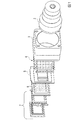
図1は、本発明の実施形態に係る撮像装置の構成を概略的に示す分解斜視図である。
図1に示すように、撮像装置1は、レンズ2、AFユニット3、ガラス部材4、カバー部材5、半導体素子6及び駆動システム7を備える。撮像装置1は、特に制限されないが、例えばスマートフォンなどのモバイル機器に搭載されるカメラである。半導体素子6は、例えば撮像素子である。本実施形態では、駆動システム7が、撮像素子としての半導体素子6を駆動することによって手振れ補正及び焦点調整のうちの一方又は双方を行う。
FIG. 1 is an exploded perspective view schematically showing the configuration of the image pickup apparatus according to the embodiment of the present invention.
As shown in FIG. 1, the imaging device 1 includes a lens 2, an
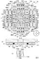
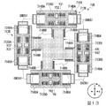
図2(a)は、図1における駆動システム7の構成を概略的に示す平面図、図2(b)は、図1(a)の線I−I’に沿う断面図であり、図3は、図2(b)の部分拡大断面図である。
駆動システム7は、互いに直交する3方向(例えば、XYZ方向)の並進及び3方向の軸回りの回転のうちの少なくとも1つの動きをするアクチュエータ71Aと、アクチュエータ71Aに伴って移動する半導体素子6と該半導体素子6の外方に位置する枠体72とを接続するフレキシブル配線体73Aとを備える。本実施形態では、アクチュエータ71Aは、互いに直交するXYZ方向のうちのX方向及びY方向への並進、並びにZ方向の軸回りの回転(θz方向)の動きを行う。
2A is a plan view schematically showing the configuration of the
The
フレキシブル配線体73Aは、半導体素子6が載置され、半導体素子6と電気的に接続される主部731Aと、主部731Aから枠体72に向かって延出し、三次元的に曲げられた複数の腕部732Aとを有する。本実施形態では、フレキシブル配線体73Aは、4つの腕部732Aを有しており、4つの腕部732Aは、例えば、平面視で主部731Aの中心を通ってY方向に沿う線を基準として線対称に配置されている。
The
腕部732Aは、主部731Aの主面731aと交わる主面732aを有するように曲げられ(図2(b))、更に折り返して曲げられており(図2(a))、腕部732Aの変形によって半導体素子6の横方向(X方向)、縦方向(Y方向)及び半導体素子6の主面に対して垂直な方向(Z方向)の軸回りの回転に自由度を与える。
The
フレキシブル配線体73Aは、4つの腕部732Aを有しているが、これに限らず、4つ以上の腕部732Aを有していてもよい。また、主部731Aの平面視において、複数の腕部732Aが主部731Aを基準として対称に配置され、複数の腕部732Aが折り返して曲げられていることによって弾性変形による力が釣り合った状態が維持されているのが好ましい。但し、必ずしも弾性変形による力が釣り合った状態である必要は無い。複数の腕部732Aが主部731Aを基準として対称に配置され、複数の腕部732Aが折り返して曲げられており、且つ、複数の腕部732Aのいずれにも弾性変形による力が生じていない状態が維持されていてもよい。これにより、アクチュエータ71Aの駆動電力を小さくすることができ、省電力化を図ることができる。
The
腕部732Aは、具体的には、主部731Aの主面731aに対して実質的に垂直な主面732aを有する第一部位732Aaと、第一部位732Aaの一端に設けられ、折り返して湾曲した第二部位732Abと、第一部位732Aaと対向配置される第三部位732Acと、第三部位732Acの一端に設けられ、主部731Aの主面731aと実質的に平行な主面732bを有する第四部位732Adとを有する。第一部位732Aa、第二部位732Ab及び第三部位732Acは、主部731Aの主面731aに対して実質的に垂直に配置されている。
Specifically, the
主部731Aは、接着層74Aを介してステージ部711Aの上面711aに固定されている。また、腕部732Aの第一部位732Aaは、接着層75Aを介してステージ部711Aの側面711bに固定され、腕部732Aの第四部位732Adは、接着層76Aを介して枠体72の上面72aに固定されている(図3)。主部731Aは、ステージ部711AのX方向、Y方向及び/又はθz方向への移動に伴って移動し、腕部732Aの第二部位732Ab及び第三部位732Acが、主部731Aの移動に伴って変形する。
The
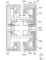
図4は、図2(a)におけるフレキシブル配線体73Aの展開図である。本実施形態では、図4中の線L1,L1でフレキシブル配線体73Aを山折りとし、更に4つの腕部732Aのそれぞれの中間部を折り返して曲げることにより、図2(a)及び図2(b)に示すような三次元構造が形成される。
FIG. 4 is a development view of the
フレキシブル配線体73Aは、樹脂層733Aと、樹脂層733A上に並べて形成され、互いに絶縁された線状の複数の導電層734Aとで構成されている。すなわち、主部731A及び腕部732Aは、樹脂層733Aと、樹脂層733A上に並べて形成され、互いに絶縁された線状の複数の導電層734Aとで構成されている。樹脂層733Aは、単層で構成されてもよいし、異なる材料からなる複数層で構成されてもよい。複数の導電層734Aも、単層で構成されてもよいし、異なる材料からなる複数層で構成されてもよい。導電層734Aの一端部734Aaは、金属で構成されるボンディングワイヤなどのワイヤ部77を介して半導体素子6に電気的に接続され、他端部734Abは、不図示のコネクタ端子に電気的に接続される(図3)。樹脂層733Aの厚みは、例えば10μm〜30μmであり、導電層734Aの厚みは、例えば5μm〜15μmである。樹脂層733Aは、例えばポリイミド(PI)で構成され、導電層734Aは、例えば銅(Cu)で構成される。この図では、導電層は1層になっているが、より複雑な配線を行うため多層になっていてもよい。また、導電層の上に絶縁保護膜が形成されていてもよい。さらに、この図では、半導体素子6だけがフレキシブル配線体73Aに搭載されているが、他の素子が搭載されていてもよい。
The
複数の腕部732Aは、全体で20線以上の導電層734Aを有するのが好ましい。本実施形態では、腕部732Aに5つの導電層734Aが設けられており、複数の腕部732Aが、全体で20線の導電層734Aを有している。但し、全体で20線以上の導電層734Aが設けられていれば、腕部の数及び各腕部の導電層の線数又は層数に制限は無く、仕様に応じて適宜変更することができる。これにより、半導体素子6の高機能化等に伴う配線の増大に十分に対応することができる。また、本実施形態では、平面視で20線の導電層734Aの線幅が同じであるが、これに限られず、20線の導電層734Aの線幅が異なっていてもよい。例えば、複数の導電層734Aが、通信用の幅狭な導電層と電力用の幅広な導電層とを含んでいてもよい。これにより、複数の導電層734Aにおいて、高速通信用の高周波信号を流す導電層と、撮像素子駆動用の大電流を流す導電層とを設けることができ、フレキシブル配線体73Aに高速通信用の高周波信号と撮像素子駆動用の大電流との双方を流すことが可能となる。
It is preferable that the plurality of
フレキシブル配線体73Aの形成方法は、特に制限されず、銅積層板の銅箔をエッチングして回路形成を行うサブトラクティブ法や、導電層を有する絶縁基材に電界銅めっきで回路を形成するセミアディティブ法などの方法を用いて形成することができる。
The method for forming the
図5(a)は、図2(b)におけるアクチュエータ71Aの構成を概略的に示す底面図であり、図5(b)は、図5(b)は、図5(a)の線II−II’に沿う概略断面図、図5(c)は、図5(b)における絶縁部の拡大断面図である。本実施形態では、アクチュエータ71Aは、静電アクチュエータである。
FIG. 5A is a bottom view schematically showing the configuration of the
アクチュエータ71Aは、基板8に固定される複数の基部712Aと、フレキシブル配線体73Aの主部731A及び半導体素子6がステージ部711Aを介して取り付けられる可動部713Aと、基部712Aと可動部713Aとを連結する複数のばね部714Aとを有する。アクチュエータ71Aは、基部712A、可動部713A及び複数のばね部714Aを有していればその形態に制限は無いが、小型化や製造容易性の観点から、例えばMEMSによって形成されている。
The
具体的には、複数の基部712Aは、X方向に関してアクチュエータ71Aの一端側に配置された固定部位X11,X12,GND14,GND15,GND14,θ12と、X方向に関してアクチュエータ71Aの他端側に配置された固定部位X21,X22,θ22,GND23,GND25,GND23とを有する。固定部位の符号「X」は、可動部713AをX方向に並進させる際に電圧が付与される部位であることを示し、符号「GND」は接地される部位、符号「θ」はθz方向に回転させる際に電圧が付与される部位であることを示す。固定部位X11,X12は、取出電極79Aを介して基板8に接続されている。他の固定部位も同様の構成であるので、その説明を省略する。
Specifically, the plurality of
2つの固定部位X11,X12には、櫛歯電極の一方の櫛歯が形成されており、他方の櫛歯が後述の第一可動部713AAに形成されている。4つの固定部位GND14,GND14,GND15,θ12は、それぞれ第一ばね部714AAを介して後述の第一可動部713AAに接続されている。また、2つの固定部位X21,X22には、それぞれ櫛歯電極の一方の櫛歯が形成されており、他方の櫛歯が後述の第一可動部713ABに形成されている。4つの固定部位θ22,GND23,GND25,GND23は、それぞれ第一ばね部714AAを介して後述の第一可動部713ABに接続されている。 One of the comb teeth of the comb-teeth electrode is formed on the two fixed portions X11, X12, and the other comb-teeth is formed on the first movable portion 713AA described later. The four fixed parts GND14, GND14, GND15, θ12 are respectively connected to a later-described first movable part 713AA via a first spring part 714AA. Further, one comb tooth of the comb tooth electrode is formed on each of the two fixed portions X21 and X22, and the other comb tooth is formed on the first movable portion 713AB described later. The four fixed parts θ22, GND23, GND25, and GND23 are connected to a first movable part 713AB, which will be described later, via a first spring part 714AA.
また、複数の基部712Aは、Y方向に関してアクチュエータ71Aの一端側に配置された固定部位Y11,Y12,GND31,GND35,GND31,θ31を有し、且つY方向に関してアクチュエータ71Aの他端側に配置された固定部位Y21,Y22,θ41,GND42,GND45,GND42を有する。固定部位の符号「Y」は、可動部713AをY方向に移動させる際に電圧が付与される部位、符号「GND」は接地される部位、符号「θ」はθz方向に回転させる際に電圧が付与される部位であることを示す。
The plurality of
2つの固定部位Y11,Y12には、櫛歯電極の一方の櫛歯が形成されており、他方の櫛歯が後述の第一可動部713ACに形成されている。4つの固定部位GND31,GND35,GND31,θ31は、それぞれ第一ばね部714AAを介して後述の第一可動部713ACに接続されている。また、2つの固定部位Y21,Y22には、それぞれ櫛歯電極の一方の櫛歯が形成されており、他方の櫛歯が後述の第一可動部713ADに形成されている。4つの固定部位θ22,GND23,GND25,GND23は、それぞれ第一ばね部714AAを介して後述の第一可動部713ADに接続されている。 One of the comb teeth of the comb-teeth electrode is formed on the two fixed portions Y11 and Y12, and the other comb-teeth is formed on the first movable portion 713AC described later. The four fixed parts GND31, GND35, GND31, θ31 are respectively connected to a first movable part 713AC described later via a first spring part 714AA. Further, one comb tooth of the comb tooth electrode is formed on each of the two fixed portions Y21 and Y22, and the other comb tooth is formed on the first movable portion 713AD described later. The four fixed parts θ22, GND23, GND25, GND23 are respectively connected to a first movable part 713AD described later via a first spring part 714AA.
可動部713Aは、後述する第二可動部の四方(XY方向)に配置された4つの第一可動部713AA,713AB,713AC,713ADと、4つの第一可動部713AA〜713ADの中央部に配置され、4つの第一可動部713AA〜713ADと複数の第二ばね部714ABを介して連結され、平面視で略十字形の第二可動部713AEと、第二可動部713AEの中央部に配置され、第二可動部713AEと複数の第三ばね部714ACを介して連結された、平面視で略X字形の第三可動部713AFとを有する。
The
第一可動部713AA,713AB,713AC,713ADは、例えば平面視で略井桁状の枠体である。第一可動部713AAのY方向両側方には固定部位GND14,GND15,GND14,θ12が配置され、第一可動部713AAの内側には固定部位X11,X12が配置されている。また、第一可動部713ABのY方向両側方には固定部位θ22,GND23,GND25,GND23が配置され、第一可動部713ABの内側には固定部位X21,X22が配置されている。同様にして、第一可動部713ACのX方向両側方には固定部位GND31,GND35,GND31,θ31が配置され、第一可動部713ACの内側には固定部位Y11,Y12が配置されている。また、第一可動部713ADのX方向両側方には固定部位θ41,GND42,GND45,GND42が配置され、第一可動部713ADの内側には固定部位Y21,Y22が配置されている。 The first movable portions 713AA, 713AB, 713AC, 713AD are, for example, substantially cross-shaped frame bodies in a plan view. Fixed parts GND14, GND15, GND14, θ12 are arranged on both sides of the first movable part 713AA in the Y direction, and fixed parts X11, X12 are arranged inside the first movable part 713AA. Fixed parts θ22, GND23, GND25, GND23 are arranged on both sides of the first movable part 713AB in the Y direction, and fixed parts X21, X22 are arranged inside the first movable part 713AB. Similarly, fixed parts GND31, GND35, GND31, θ31 are arranged on both sides of the first movable part 713AC in the X direction, and fixed parts Y11, Y12 are arranged inside the first movable part 713AC. Fixed parts θ41, GND42, GND45, GND42 are arranged on both sides of the first movable part 713AD in the X direction, and fixed parts Y21, Y22 are arranged inside the first movable part 713AD.
固定部位GND14,GND15,GND14,θ12は、それぞれ第一ばね部714AAを介して第一可動部713AAに連結されている。固定部位θ22,GND23,GND25,GND23は、それぞれ第一ばね部714AAを介して第一可動部713ABに連結されている。固定部位GND31,GND35,GND31,θ31は、それぞれ第一ばね部714AAを介して第一可動部713ACに連結されている。固定部位θ41,GND42,GND45,GND42は、それぞれ第一ばね部714AAを介して第一可動部713ADに連結されている。また、複数の第一ばね部714AAは、機械的な接続部としての機能に加えて、電気的な接続部としても機能する。 The fixed parts GND14, GND15, GND14, θ12 are respectively connected to the first movable part 713AA via the first spring part 714AA. The fixed parts θ22, GND23, GND25, and GND23 are respectively connected to the first movable part 713AB via the first spring part 714AA. The fixed parts GND31, GND35, GND31, θ31 are respectively connected to the first movable part 713AC via the first spring part 714AA. The fixed parts θ41, GND42, GND45, GND42 are respectively connected to the first movable portion 713AD via the first spring portion 714AA. Further, the plurality of first spring portions 714AA also function as electrical connection portions in addition to the function as mechanical connection portions.
第一可動部713AAには、固定部位GND14と固定部位θ12,GND15とを絶縁するための絶縁部715AA,715ABが設けられている。第一可動部713ABには、固定部位GND23と固定部位θ22,GND25とを絶縁するための絶縁部715AC,715ADが設けられている。第一可動部713ACには、固定部位GND31と固定部位θ31,GND35とを絶縁するための絶縁部715AE,715AFが設けられている。第一可動部713ADには、固定部位GND42と固定部位θ41,GND45とを絶縁するための絶縁部715AG,715AHが設けられている。上記絶縁部は、例えば、窒化ケイ素(SiN)、ポリシリコン(p−Si)等の材料からなる1層又は複数層で構成され、トレンチアイソレーション等によって形成される。 The first movable portion 713AA is provided with insulating portions 715AA and 715AB for insulating the fixed portion GND14 from the fixed portions θ12 and GND15. The first movable portion 713AB is provided with insulating portions 715AC and 715AD for insulating the fixed portion GND23 from the fixed portions θ22 and GND25. The first movable portion 713AC is provided with insulating portions 715AE and 715AF for insulating the fixed portion GND31 from the fixed portions θ31 and GND35. The first movable portion 713AD is provided with insulating portions 715AG and 715AH for insulating the fixed portion GND42 from the fixed portions θ41 and GND45. The insulating portion is composed of, for example, one layer or a plurality of layers made of a material such as silicon nitride (SiN) or polysilicon (p-Si), and is formed by trench isolation or the like.
本実施形態において、固定部位X11は固定部位X21と同電位であり、固定部位X12は固定部位X22と同電位である。固定部位Y11は固定部位Y21と同電位、固定部位Y12は固定部位Y22と同電位である。固定部位X11,X21に電圧を印加すると、第一可動部713AA,713ABがX方向の一方(例えば+X方向)に移動し、固定部位X12,X22に電圧を印加すると、第一可動部713AA,713ABがX方向の他方(例えば−X方向)に移動する。一方、固定部位Y11,Y21に電圧を印加すると、第一可動部713AC,713ADがY方向の一方(例えば+Y方向)に移動し、固定部位Y12,Y22に電圧を印加すると、第一可動部713AC,713ADがY方向の他方(例えば−X方向)に移動する。 In the present embodiment, the fixed part X11 has the same potential as the fixed part X21, and the fixed part X12 has the same potential as the fixed part X22. The fixed portion Y11 has the same potential as the fixed portion Y21, and the fixed portion Y12 has the same potential as the fixed portion Y22. When a voltage is applied to the fixed parts X11, X21, the first movable parts 713AA, 713AB move in one of the X directions (for example, +X direction), and when a voltage is applied to the fixed parts X12, X22, the first movable parts 713AA, 713AB. Moves in the other X direction (for example, the -X direction). On the other hand, when a voltage is applied to the fixed parts Y11 and Y21, the first movable parts 713AC and 713AD move to one side in the Y direction (for example, +Y direction), and when a voltage is applied to the fixed parts Y12 and Y22, the first movable part 713AC. , 713AD moves in the other Y direction (for example, the −X direction).
第二可動部713AEは、例えば平面視で略十字形の外郭を有する枠状体であり、8つの第二ばね部714ABを介して4つの第一可動部713AA,713AB,713AC,713ADに連結されている。第二可動部713AEのX方向一端側には2つの第二ばね部714ABが配置され、その他端側にも2つの第二ばね部714ABが配置されている。また、第二可動部713AEのY方向一端側に2つの第二ばね部714ABが配置され、その他端側にも2つの第二ばね部714ABが配置されている。第二ばね部714ABは、各第二可動部が一方向のみに移動するように設計される。 The second movable portion 713AE is, for example, a frame-shaped body having a substantially cruciform outer shape in a plan view, and is connected to the four first movable portions 713AA, 713AB, 713AC, 713AD via eight second spring portions 714AB. ing. Two second spring parts 714AB are arranged on one end side in the X direction of the second movable part 713AE, and two second spring parts 714AB are also arranged on the other end side. Further, the two second spring portions 714AB are arranged on one end side in the Y direction of the second movable portion 713AE, and the two second spring portions 714AB are also arranged on the other end side. The second spring portion 714AB is designed so that each second movable portion moves in only one direction.
第二可動部713AEには、複数の櫛歯電極を構成する一方の櫛歯の複数が形成されており、複数の櫛歯電極を構成する他方の櫛歯の複数が第三可動部713AFに形成されている。本実施形態では、4つの櫛歯電極が、第二可動部713AEと第三可動部713AFとの間であって第三可動部713AFの中心を基準として180°回転対称となるように配置されている。 The second movable portion 713AE is formed with a plurality of one comb teeth forming a plurality of comb tooth electrodes, and the plurality of the other comb teeth forming a plurality of comb tooth electrodes is formed in the third movable portion 713AF. Has been done. In this embodiment, the four comb-teeth electrodes are arranged between the second movable portion 713AE and the third movable portion 713AF so as to be 180° rotationally symmetrical with respect to the center of the third movable portion 713AF. There is.
また、第二可動部713AEは、第三可動部713AFを囲繞するように設けられた6つの移動部位θ51,θ52,GND55,θ61,θ62,GND65を有する。移動部位θ51,θ52,GND55,θ61,θ62,GND65は、第三可動部713AFの中心を基準として180°回転対称となるように配置されている。移動部位の符号「GND」は接地された部位、符号「θ」はθz方向に回転させる際に電圧が付与される部位であることを示す。 Further, the second movable portion 713AE has six moving portions θ51, θ52, GND55, θ61, θ62, GND65 provided so as to surround the third movable portion 713AF. The moving parts θ51, θ52, GND55, θ61, θ62, and GND65 are arranged so as to be 180° rotationally symmetric with respect to the center of the third movable portion 713AF. The reference symbol “GND” of the moving portion indicates a grounded portion, and the reference numeral “θ” indicates a portion to which a voltage is applied when rotating in the θz direction.
移動部位θ51は、第二ばね部714ABと第一ばね部714AAを介して固定部位θ31と連結されている。移動部位θ52は、第二ばね部714ABと第一ばね部714AAを介して固定部位θ22と連結されている。移動部位GND55は、第二ばね部714ABと第一ばね部714AAを介して固定部位GND15,GND35にそれぞれ連結されている。移動部位θ61は、第二ばね部714ABと第一ばね部714AAを介して固定部位θ41と連結されている。移動部位θ62は、第二ばね部714ABと第一ばね部714AAを介して固定部位θ12と連結されている。移動部位GND65は、第二ばね部714ABと第一ばね部714AAを介して固定部位GND25,GND45にそれぞれ連結されている。また、複数の第二ばね部714ABと第一ばね部714AAは、機械的な接続部としての機能に加えて、電気的な接続部としても機能する。 The moving portion θ51 is connected to the fixed portion θ31 via the second spring portion 714AB and the first spring portion 714AA. The moving portion θ52 is connected to the fixed portion θ22 via the second spring portion 714AB and the first spring portion 714AA. The moving portion GND55 is connected to the fixed portions GND15 and GND35 via the second spring portion 714AB and the first spring portion 714AA, respectively. The moving portion θ61 is connected to the fixed portion θ41 via the second spring portion 714AB and the first spring portion 714AA. The moving portion θ62 is connected to the fixed portion θ12 via the second spring portion 714AB and the first spring portion 714AA. The moving portion GND65 is connected to the fixed portions GND25 and GND45 via the second spring portion 714AB and the first spring portion 714AA, respectively. The plurality of second spring portions 714AB and the first spring portions 714AA also function as electrical connection portions in addition to the function as mechanical connection portions.
また、6つの移動部位θ51,θ52,GND55,θ61,θ62,GND65のうちの隣接する移動部位間には、絶縁部716AA,716AB,716AC,716AD,716AE,716AFが設けられている。上記絶縁部は、例えば、SiN、p−Si等の材料からなる1層又は複数層で構成され、トレンチアイソレーション等によって形成される。本実施形態では、図5(c)に示すように、絶縁部716ABは、SiNからなる第一層716ABaと、p−Siからなる第二層716ABbとを有する。絶縁部716AA,716AC〜716AFも同様の構成であるので、その説明を省略する。 Insulating parts 716AA, 716AB, 716AC, 716AD, 716AE, 716AF are provided between adjacent moving parts of the six moving parts θ51, θ52, GND55, θ61, θ62, GND65. The insulating portion is composed of, for example, one layer or a plurality of layers made of a material such as SiN or p-Si, and is formed by trench isolation or the like. In the present embodiment, as shown in FIG. 5C, the insulating portion 716AB has a first layer 716ABa made of SiN and a second layer 716ABb made of p-Si. The insulating portions 716AA and 716AC to 716AF have the same configuration, and thus the description thereof will be omitted.
第三可動部713AFは、例えば平面視で略X字形の枠状体であり、複数の第三ばね部714ACを介して第二可動部713AEに連結されている。複数の第三ばね部714ACは、機械的な接続部としての機能に加えて、電気的な接続部としても機能する。第三可動部713AFのX方向一端側には第三ばね部714ACが配置され、その他端側にも第三ばね部714ACが配置されている。また、第三可動部713AFのY方向一端側に第三ばね部714ACが配置され、その他端側にも第三ばね部714ACが配置されている。第三可動部713AFは、接着層78Aを介してステージ部711Aに固定されている(図2(b))。
The third movable portion 713AF is, for example, a substantially X-shaped frame body in a plan view, and is connected to the second movable portion 713AE via a plurality of third spring portions 714AC. The plurality of third spring parts 714AC also function as electrical connection parts in addition to the function as mechanical connection parts. The third spring portion 714AC is arranged on one end side in the X direction of the third movable portion 713AF, and the third spring portion 714AC is also arranged on the other end side. Further, the third spring portion 714AC is arranged on one end side in the Y direction of the third movable portion 713AF, and the third spring portion 714AC is also arranged on the other end side. The third movable portion 713AF is fixed to the
本実施形態において、移動部位θ51は固定部位θ31と同電位であり、移動部位θ52は固定部位θ22と同電位である。移動部位θ61は固定部位θ41と同電位、移動部位θ62は固定部位θ12と同電位である。また、移動部位GND55,GND65は、固定部位GND35,GND45と同電位である。そして、移動部位θ51,θ61に同電圧を印加すると、第三可動部713AFがθz方向の一方(例えば時計回り)に移動し、移動部位θ52,θ62に同電圧を印加すると、第三可動部713AFがθz方向の他方(例えば反時計回り)に移動する。 In the present embodiment, the moving part θ51 has the same potential as the fixed part θ31, and the moving part θ52 has the same potential as the fixed part θ22. The moving part θ61 has the same potential as the fixed part θ41, and the moving part θ62 has the same potential as the fixed part θ12. The moving parts GND55 and GND65 have the same potential as the fixed parts GND35 and GND45. Then, when the same voltage is applied to the moving parts θ51 and θ61, the third movable part 713AF moves to one side in the θz direction (for example, clockwise), and when the same voltage is applied to the moving parts θ52 and θ62, the third movable part 713AF. Moves in the other direction (eg, counterclockwise) in the θz direction.
上記のように所定の固定部位及び/又は移動部位に電圧を印加することにより、第一可動部713AA〜713AD及び第二可動部713AEは、X方向及び/又はY方向に並進し、第三可動部713AFは、θz方向に回転する。したがって、第三可動部713AFは、X方向、Y方向及び/又はθz方向に移動する。ステージ部711Aは、第三可動部713AFの移動に伴ってX方向、Y方向及び/又はθz方向に移動し、ステージ部711Aの移動に伴ってフレキシブル配線体73Aの主部731AがXd方向、Y方向及び/又はθz方向に移動する。フレキシブル配線体73Aの複数の腕部732Aは、主部731Aの移動に伴って容易に変形し、追従する。
By applying the voltage to the predetermined fixed part and/or the moving part as described above, the first movable parts 713AA to 713AD and the second movable part 713AE are translated in the X direction and/or the Y direction, and the third movable part is moved. The unit 713AF rotates in the θz direction. Therefore, the third movable portion 713AF moves in the X direction, the Y direction, and/or the θz direction. The
アクチュエータ71Aの形成方法は、特に制限されず、例えば、酸化膜の両面にシリコン単結晶が形成されたSOI等の基板を用い、ハンドル層及び活性層にDRIE(深堀り反応性エッチング)などのエッチング加工を施すことによって形成することができる。また、アクチュエータ71A内の上記絶縁部は、DRIE、LPCVD、研磨などを組み合わせて形成することができる。
The method of forming the
駆動システム7は、上記可動部及び上記複数のばね部のうちの少なくとも1つの変位を測定する、少なくとも1つの変位センサを備えていてもよい。例えば、駆動システム7は、第三可動部713AFの変位を測定するのに、駆動用櫛歯電極を用いてもよいし、別の変位センサを更に備えていてもよい。変位センサからの信号を不図示の制御部に入力し、該信号に基づいてアクチュエータ71Aの駆動を制御することにより、半導体素子6のより高精度な位置制御を実現することができる。
The
上述したように、本実施形態によれば、フレキシブル配線体73Aが、半導体素子6が載置され、半導体素子6と電気的に接続される主部731Aと、主部731Aから枠体72に向かって延出し、三次元的に曲げられた複数の腕部732Aとを有するので、主部731Aと一体成形された複数の腕部732Aの主面732aが主部731Aの主面731aに対して非平行となり、複数の腕部732Aが、ステージ部711Aに固定された主部731Aの並進(X方向及び/又はY方向)や回転(θz方向)に対して面外方向に容易且つ十分に屈曲し、アクチュエータ71Aの移動が阻害され難く、その結果、主部731A上に載置された半導体素子6の位置決め性能を向上することができる。また、腕部732Aに通信用の導電層と電力用の導電層とを設けることで、高速通信用の高周波信号と撮像素子駆動用の大電流の双方を安定的に流すことができる。また、フレキシブル配線体73Aは、フレキシブル配線体73Aの展開体に簡単な曲げ加工を施すことで形成できるので、煩雑な組立工程が不要で大量生産にも対応することができる。
As described above, according to the present embodiment, the
また、主部731Aの平面視において、複数の腕部732Aが主部731Aを基準として対称に配置され、複数の腕部732Aが折り返して曲げられていることによって弾性変形による力が釣り合った状態が維持されているので、アクチュエータ71AがMEMS等で形成されていて発生力が小さい場合であっても、フレキシブル配線体73Aの剛性に因る抵抗力が小さくなるため、アクチュエータ71Aの移動が阻害され難く、半導体素子6の高精度の移動を実現することができる。
Further, in a plan view of the
更に、腕部732Aは、主部731Aの主面731aに対して実質的に垂直な主面732aを有する第一部位732Aaと、第一部位732Aaの一端に設けられ、折り返して湾曲した第二部位732Abと、第一部位732Aaと対向配置される第三部位732Acとが、主部731Aの主面731aに対して実質的に垂直に配置されるので、複数の腕部732Aが、ステージ部711Aに固定された主部731Aの並進(X方向及び/又はY方向)や回転(θz方向)に対して確実に追従することができ、主部731A上に載置された半導体素子6の位置決め性能を更に向上できると共に、接続信頼性を向上することができる。
Further, the
また、本実施形態によれば、アクチュエータ71Aに複数の絶縁部715AA〜715AF,716AA〜716AFが形成されており、X方向への並進を行う駆動機構及び回路、Y方向への並進を行う駆動機構及び回路、並びにθz方向の回転を行うための駆動機構及び回路がそれぞれ電気的に独立して設けられるため、X方向、Y方向及び/又はθz方向への任意の移動を実現することができる。また、アクチュエータ71Aの駆動回路が基板8の不図示の回路に接続されるので、アクチュエータ71Aの配線と半導体素子6の配線(フレキシブル配線体73Aの導電層)とを、ステージ部711Aを基準として上下に分けて形成することができ、これらの配線の物理的な干渉を確実に防止することができる。また、アクチュエータ71Aにおける複数の基部712Aを基板8にフリップチップ接続することにより、アクチュエータ71Aの可動部713Aの微細部分を保護することができる。
Further, according to the present embodiment, the
図6(a)は、図2(a)における駆動システム7の変形例を示す平面図、図6(b)は、図6(a)の線III−III’に沿う断面図であり、図7は、図6(b)の部分拡大断面図である。図6(a)における駆動システムは、主にステージ部711Aを有さず、アクチュエータ71Aが接着層80Aを介してフレキシブル配線体73Aに直接接続されている点で、図2(a)における駆動システム7の構成と異なる。図2(a)における駆動システム7と同一の構成については、同一の符号を付してその説明を省略する。
FIG. 6A is a plan view showing a modified example of the
図6(a)のフレキシブル配線体73Aは、展開体の状態で図2(a)のフレキシブル配線体73Aと同一の構成を有し、加工により三次元構造を形成した状態では図2(a)のフレキシブル配線体73Aと異なる構成を有している。フレキシブル配線体73Aは、図6(b)に示すように、主部731Aと腕部732Aで画定され、半導体素子6が収容される収容部81Aを有している。主部731Aは、図7に示すように、接着層82Aを介して半導体素子6の下面6aに固定されている。腕部732Aの第一部位732Aaは、接着層83Aを介して半導体素子6の側面6bに固定されている(図7)。また、導電層734Aの一端部734Aaは、超音波接続、熱圧着、導電性接着材を用いた接続等により形成された接合部84Aを介して半導体素子6に電気的に接続され、他端部734Abは、不図示のコネクタ端子に電気的に接続される。
The
図8は、図6(a)におけるフレキシブル配線体73Aの展開図である。本変形例では、図8中の線L2,L2でフレキシブル配線体73Aを山折りとし、更に4つの腕部732Aのそれぞれの中間部を折り返して曲げることにより、図6(a)及び図6(b)に示すような三次元構造が形成される。
FIG. 8 is a development view of the
このように、本変形例によれば、ステージ部711Aを有さない駆動システム7にもフレキシブル配線体73Aを適用することができる。すなわち、フレキシブル配線体73Aが、半導体素子6が載置され、半導体素子6と電気的に接続される主部731Aと、主部731Aから枠体72に向かって延出し、三次元的に曲げられた複数の腕部732Aとを有するので、主部731Aと一体成形された複数の腕部732Aの主面732aが主部731Aの主面731aに対して非平行となり、複数の腕部732Aが、ステージ部711Aに固定された主部731Aの並進(X方向及び/又はY方向)や回転(θz方向)に対して面外方向に容易且つ十分に屈曲し、アクチュエータ71Aの移動が阻害され難く、その結果、主部731A上に載置された半導体素子6の位置決め性能を向上することができる。また、ワイヤ部を設けずに接合部84Aを設けて半導体素子6とフレキシブル配線体73Aとを電気的に接続するので、半導体素子6及び駆動システム7を合わせた構成の低背化に寄与することができる。
As described above, according to this modification, the
図9は、図4におけるフレキシブル配線体の他の変形例を示す平面図である。図10(a)は、図9のフレキシブル配線体をアクチュエータに搭載した状態を示す部分平面図であり、図10(b)は、図10(a)の部分断面図である。図9のフレキシブル配線体では、腕部の形状が異なる点で、図4のフレキシブル配線体の構成と異なる。 FIG. 9 is a plan view showing another modification of the flexible wiring body in FIG. 10A is a partial plan view showing a state in which the flexible wiring body of FIG. 9 is mounted on an actuator, and FIG. 10B is a partial cross-sectional view of FIG. 10A. The flexible wiring body of FIG. 9 differs from the flexible wiring body of FIG. 4 in that the shape of the arm portion is different.
図9に示すように、フレキシブル配線体73Bは、半導体素子6が載置され、半導体素子6と電気的に接続される主部731Bと、主部731Bから枠体72(図2(a)及び図2(b)参照)に向かって延出し、三次元的に曲げられた複数の腕部732Bとを有する。
As shown in FIG. 9, the
腕部732Bは、図10(a)及び図10(b)に示すように、主部731Bの主面731bに対して実質的に垂直な主面732cを有する第一部位732Baと、第一部位732Baの一端に設けられ、折り返して湾曲した第二部位732Bbと、第一部位732Baと対向配置される第三部位732Bcと、第三部位732Bcの一端に設けられ、主部731Bの主面731bと実質的に平行な主面732dを有する第四部位732Adとを有する。第一部位732Ba、第二部位732Bb及び第三部位732Bcは、主部731Bの主面731bに対して実質的に垂直に配置されている(図10(b))。
As shown in FIGS. 10A and 10B, the
第四部位732Bdは、第三部位732Bcに対して垂直に配置された延出部732Bdaと、延出部732Bdaに対して垂直に配置された延出部732Bdbとを有する(図9)。フレキシブル配線体73Bをアクチュエータ71Aに搭載した状態では(図10(a))、延出部732Bdaは、平面視で主部731Bから離れる方向(X方向)に延出しており、延出部732Bdbは、延出部732Bdaから横方向(Y方向)に延出している。隣接する2つの腕部732Bに設けられた2つの延出部732Bdbは、横方向(Y方向)延出すると共に、互いに離れる方向に延出している。また、本変形例では、第四部位732Bdは、主部731Bと異なる平面上に設けられており、主部731Bの下方に配置されている。
The fourth portion 732Bd has an extending portion 732Bda arranged vertically to the third portion 732Bc and an extending portion 732Bdb arranged vertically to the extending portion 732Bda (FIG. 9). When the
本変形例では、延出部732Bdbに導電層734Bの他端部734Bbが設けられており、導電層734Bの一端部734Baが半導体素子6に電気的に接続され、他端部734Bbが、不図示のコネクタ端子に電気的に接続される。また、フレキシブル配線体73Bが三次元的に曲げられた状態において、導電層734Bの他端部734Bbは、Z方向に関して樹脂層733Bの下側(裏側)に配置される(図10(b))。
In the present modification, the extension portion 732Bdb is provided with the other end portion 734Bb of the
腕部732Bは、主部731Bと第一部位732Baとの間に、折り曲げの際にマージン部となる第五部位732Beを有していてもよい。また、第五部位732Beの幅方向(Y方向)寸法が、主部731Bの幅方向寸法よりも小さいことが好ましい。これにより、曲げ加工によって第一部位732Baを形成し易くなり、また、折り曲げられた部分での導電層734Bの座屈を抑制することができ、導電層734Bの電気的な接続信頼性を更に向上することができる。
The
本変形例によれば、第四部位732Bdが、第三部位732Bcに対して垂直に配置された延出部732Bdaと、延出部732Bdaに対して垂直に配置された延出部732Bdbとを有するので、コネクタ端子に挿入される第四部位732Bdの設計の自由度を向上することができる。 According to this modification, the fourth portion 732Bd has the extending portion 732Bda arranged perpendicular to the third portion 732Bc and the extending portion 732Bdb arranged perpendicular to the extending portion 732Bda. Therefore, the degree of freedom in designing the fourth portion 732Bd inserted into the connector terminal can be improved.
図11は、図4におけるフレキシブル配線体の他の変形例を示す平面図である。図12(a)は、図11のフレキシブル配線体をアクチュエータに搭載した状態を示す部分平面図であり、図12(b)は、図12(a)の部分断面図である。 FIG. 11 is a plan view showing another modification of the flexible wiring body in FIG. 12A is a partial plan view showing a state in which the flexible wiring body of FIG. 11 is mounted on an actuator, and FIG. 12B is a partial cross-sectional view of FIG. 12A.
図11に示すように、フレキシブル配線体73Cは、半導体素子6が載置され、半導体素子6と電気的に接続される主部731Cと、主部731Cから枠体72(図2(a)及び図2(b)参照)に向かって延出し、三次元的に曲げられた複数の腕部732Cとを有する。
As shown in FIG. 11, the
腕部732Cは、図12(a)及び図12(b)に示すように、主部731Cの主面731cに対して実質的に垂直な主面732eを有する第一部位732Caと、第一部位732Caの一端に設けられ、折り返して湾曲した第二部位732Cbと、第一部位732Caと対向配置される第三部位732Ccと、第三部位732Ccの一端に設けられ、主部731Cの主面731cと実質的に平行な主面732fを有する第四部位732Cdとを有する。第一部位732Ca、第二部位732Cb及び第三部位732Ccは、主部731Cの主面731cに対して実質的に垂直に配置されている。(図10(b))。
As shown in FIGS. 12A and 12B, the
第四部位732Cdは、第三部位732Ccに対して垂直に配置された延出部732Cdaと、延出部732Cdaに対して垂直に配置された延出部732Cdbとを有する(図11)。フレキシブル配線体73Cをアクチュエータ71Aに搭載した状態では(図12(a))、延出部732Cdaは、平面視で主部731Cから離れる方向(X方向)に延出しており、延出部732Cdbは、延出部732Cdaから横方向(Y方向)に延出している。隣接する2つの腕部732Cに設けられた2つの延出部732Cdbは、横方向(Y方向)延出すると共に、互いに離れる方向に延出している。また、本変形例では、第四部位732Cdは、主部731Cと同一の平面上に設けられている。
The fourth portion 732Cd has an extending portion 732Cda arranged vertically to the third portion 732Cc and an extending portion 732Cdb arranged vertically to the extending portion 732Cda (FIG. 11). When the
また、本変形例では、延出部732Cdbに導電層734Cの他端部734Cbが設けられており、導電層734Cの一端部734Caが半導体素子6に電気的に接続され、他端部734Bbが、不図示のコネクタ端子に電気的に接続される。また、フレキシブル配線体73Cが三次元的に曲げられた状態において、導電層734Cの他端部734Cbは、Z方向に関して樹脂層733Cの上側(表側)に配置される(図12(b))。
Further, in this modification, the other end 734Cb of the
本変形例によれば、第四部位732Cdが、第三部位732Ccに対して垂直に配置された延出部732Cdaと、延出部732Cdaに対して垂直に配置された延出部732Cdbとを有するので、フレキシブル配線体73Bの第四部位732Bdと同様、コネクタ端子に挿入される第四部位732Cdの設計の自由度を向上することができる。
According to this modification, the fourth portion 732Cd has the extending portion 732Cda arranged vertically to the third portion 732Cc and the extending portion 732Cdb arranged vertically to the extending portion 732Cda. Therefore, like the fourth portion 732Bd of the
図13は、図5のアクチュエータ71Aの変形例を示す底面図である。
図13に示すように、アクチュエータ71Bは、基板8(図2(b)参照)に固定される複数の基部712Bと、フレキシブル配線体73Aの主部731A及び半導体素子6が取り付けられる可動部713Bと、基部712Bと可動部713Bとを連結する複数のばね部714Bとを有する。アクチュエータ71Bは、アクチュエータ71Aと同様、例えばMEMSによって形成されている。
FIG. 13 is a bottom view showing a modified example of the
As shown in FIG. 13, the
複数の基部712Bは、X方向に関してアクチュエータ71Bの一端側に配置された固定部位X31,X32,GND51,GND51と、X方向に関してアクチュエータ71Bの他端側に配置された固定部位X41,X42,GND51,GND51とを有する。固定部位X31,X32は、不図示の取出電極を介して基板8に接続されている(図5(b)参照)。他の固定部位も同様の構成であるので、その説明を省略する。
The plurality of
2つの固定部位X31,X32には、櫛歯電極の一方の櫛歯が形成されており、他方の櫛歯が後述の第一可動部713BAに形成されている。2つの固定部位GND51,GND51は、それぞれ第一ばね部714BAを介して後述の第一可動部713BAに接続されている。また、2つの固定部位X41,X42には、それぞれ櫛歯電極の一方の櫛歯が形成されており、他方の櫛歯が後述の第一可動部713BBに形成されている。2つの固定部位GND51,GND51は、それぞれ第一ばね部714BAを介して後述の第一可動部713BBに接続されている。 One of the comb teeth of the comb-teeth electrode is formed on each of the two fixed portions X31 and X32, and the other comb-teeth is formed on the first movable portion 713BA described later. The two fixed parts GND51 and GND51 are connected to a first movable part 713BA, which will be described later, via a first spring part 714BA. Further, one comb tooth of the comb tooth electrode is formed on each of the two fixed portions X41 and X42, and the other comb tooth is formed on the first movable portion 713BB described later. The two fixed parts GND51 and GND51 are connected to a first movable part 713BB, which will be described later, via a first spring part 714BA.
また、複数の基部712Bは、Y方向に関してアクチュエータ71Bの一端側に配置された固定部位Y31,Y32,GND51,GND51を有し、且つY方向に関してアクチュエータ71Bの他端側に配置された固定部位Y41,Y42,GND51,GND51を有する。
In addition, the plurality of
2つの固定部位Y31,Y32には、櫛歯電極の一方の櫛歯が形成されており、他方の櫛歯が後述の第一可動部713BCに形成されている。2つの固定部位GND51,GND51は、それぞれ第一ばね部714BAを介して後述の第一可動部713BCに接続されている。また、2つの固定部位Y41,Y42には、それぞれ櫛歯電極の一方の櫛歯が形成されており、他方の櫛歯が後述の第一可動部713BDに形成されている。2つの固定部位GND51,GND51は、それぞれ第一ばね部714BAを介して後述の第一可動部713BDに接続されている。 One of the comb teeth of the comb-teeth electrode is formed on the two fixed portions Y31 and Y32, and the other comb-teeth is formed on the first movable portion 713BC described later. The two fixed parts GND51 and GND51 are connected to a first movable part 713BC, which will be described later, via a first spring part 714BA. Further, one comb tooth of the comb tooth electrode is formed on each of the two fixed portions Y41 and Y42, and the other comb tooth is formed on the first movable portion 713BD described later. The two fixed parts GND51 and GND51 are respectively connected to a first movable part 713BD described later via a first spring part 714BA.
可動部713Bは、後述する第二可動部の四方(XY方向)に配置された4つの第一可動部713BA,713BB,713BC,713BDと、4つの第一可動部713BA〜713BDの中央部に配置され、4つの第一可動部713BA〜713BDと複数の第二ばね部714BBを介して連結され、平面視で略風車形の第二可動部713BEとを有する。
The
第一可動部713BA,713BB,713BC,713BDは、例えば平面視で略井桁状の枠体である。第一可動部713BAのY方向両側方には固定部位GND51,GND51が配置され、第一可動部713BAの内側には固定部位X31,X32が配置されている。同様にして、第一可動部713BBのY方向両側方には固定部位GND51,GND51が配置され、第一可動部713BBの内側には固定部位X41,X42が配置されている。
また、第一可動部713BCのX方向両側方には固定部位GND51,GND51が配置され、第一可動部713BCの内側には固定部位Y31,Y32が配置されている。また、第一可動部713BDのX方向両側方には固定部位GND51,GND51が配置され、第一可動部713BDの内側には固定部位Y41,Y42が配置されている。
The first movable portions 713BA, 713BB, 713BC, 713BD are, for example, substantially cross-shaped frame bodies in a plan view. Fixed parts GND51 and GND51 are arranged on both sides of the first movable part 713BA in the Y direction, and fixed parts X31 and X32 are arranged inside the first movable part 713BA. Similarly, the fixed parts GND51 and GND51 are arranged on both sides of the first movable part 713BB in the Y direction, and the fixed parts X41 and X42 are arranged inside the first movable part 713BB.
Fixed parts GND51 and GND51 are arranged on both sides of the first movable part 713BC in the X direction, and fixed parts Y31 and Y32 are arranged inside the first movable part 713BC. Fixed parts GND51 and GND51 are arranged on both sides of the first movable part 713BD in the X direction, and fixed parts Y41 and Y42 are arranged inside the first movable part 713BD.
複数の固定部位GND51は、それぞれ第一ばね部714BAを介して第一可動部713BA〜713BDに連結されている。また、複数の第一ばね部714BAは、機械的な接続部としての機能に加えて、電気的な接続部としても機能する。 The plurality of fixed portions GND51 are connected to the first movable portions 713BA to 713BD via the first spring portions 714BA, respectively. Further, the plurality of first spring parts 714BA also function as electrical connection parts in addition to the function as mechanical connection parts.
本変形例において、固定部位X31,X32、X41,X42,Y31,Y32,Y41,Y42に任意の電圧を与えることによって、第一可動部713BA,713BB,713BC,713BDが独立に移動し,第二可動部713BEがX,Y,θz方向に移動する。例えば、固定部位X32とX41に同電圧を与えれば、第一可動部713BAと713BBは等しくX方向(右向き)に移動し、第二可動部713BEは+X方向(右向き)に移動する。また、固定部位X32,X42,Y32,Y42に同電圧を与えれば、第一可動部713BA,713BB,713BC,713BDは等しく中心方向に移動し、第二可動部713BEはθz方向(時計回り)に回転する。 In this modification, the first movable parts 713BA, 713BB, 713BC, 713BD move independently by applying an arbitrary voltage to the fixed parts X31, X32, X41, X42, Y31, Y32, Y41, Y42. The movable portion 713BE moves in the X, Y, and θz directions. For example, if the same voltage is applied to the fixed parts X32 and X41, the first movable parts 713BA and 713BB move equally in the X direction (rightward), and the second movable part 713BE moves in the +X direction (rightward). When the same voltage is applied to the fixed parts X32, X42, Y32, Y42, the first movable parts 713BA, 713BB, 713BC, 713BD move equally toward the center, and the second movable part 713BE moves in the θz direction (clockwise direction). Rotate.
第二可動部713BEは、8つの第二ばね部714BBを介して4つの第一可動部713BA,713BB,713BC,713BDに連結されている。第二可動部713BEのX方向一端側には2つの第二ばね部714BBが配置され、その他端側にも2つの第二ばね部714BBが配置されている。また、第二可動部713BEのY方向一端側に2つの第二ばね部714BBが配置され、その他端側にも2つの第二ばね部714BBが配置されている。第二ばね部714BBを適切に設計することによって、第一可動部713BAと713BBはX方向のみに、第一可動部713BCと713BDはY方向のみに移動することができる。第二可動部713BEは、接着層78Aを介してステージ部711Aに固定される(図2(b)参照)。
The second movable portion 713BE is connected to the four first movable portions 713BA, 713BB, 713BC, 713BD via the eight second spring portions 714BB. Two second spring portions 714BB are arranged on one end side in the X direction of the second movable portion 713BE, and two second spring portions 714BB are also arranged on the other end side. Further, the two second spring portions 714BB are arranged on one end side in the Y direction of the second movable portion 713BE, and the two second spring portions 714BB are also arranged on the other end side. By appropriately designing the second spring portion 714BB, the first movable portions 713BA and 713BB can move only in the X direction, and the first movable portions 713BC and 713BD can move only in the Y direction. The second movable portion 713BE is fixed to the
本変形例によれば、X方向への並進を行う駆動機構及び回路、並びにY方向への並進を行う駆動機構及び回路がそれぞれ独立して設けられ、また、X方向への上記並進とY方向への上記並進とを制御してθz方向の回転も行うため、X方向、Y方向及び/又はθz方向への移動を実現することができる。 According to this modification, a drive mechanism and a circuit that perform translation in the X direction, and a drive mechanism and a circuit that perform translation in the Y direction are independently provided, and the translation in the X direction and the Y direction are performed. Since the above translation is also controlled to rotate in the θz direction, movement in the X direction, the Y direction and/or the θz direction can be realized.
図14は、図5のアクチュエータ71Aの他の変形例を示す底面図である。
図14に示すように、アクチュエータ71Cは、基板8(図2(b)参照)に固定される複数の基部712Cと、フレキシブル配線体73Aの主部731A及び半導体素子6が取り付けられる可動部713Cと、基部712Cと可動部713Cとを連結する複数のばね部714Cとを有する。アクチュエータ71Cは、アクチュエータ71Aと同様、例えばMEMSによって形成されている。
FIG. 14 is a bottom view showing another modified example of the
As shown in FIG. 14, the
複数の基部712Cは、X方向に関してアクチュエータ71Cの一端側に配置された固定部位X51,X52,GND61,X61,X62,GND61と、X方向に関してアクチュエータ71Cの他端側に配置された固定部位X71,X72,GND61,X81,X82,GND61とを有する。固定部位X51,X52は、不図示の取出電極を介して基板8に接続されている(図5(b)参照)。他の固定部位も同様の構成であるので、その説明を省略する。
The plurality of
2つの固定部位X51,X52には、櫛歯電極の一方の櫛歯が形成されており、他方の櫛歯が後述の第一可動部713CAAに形成されている。同様にして、2つの固定部位X61,X62には、櫛歯電極の一方の櫛歯が形成されており、他方の櫛歯が後述の第一可動部713CABに形成されている。2つの固定部位GND61,GND61は、それぞれ2つの第一ばね部714CAを介して後述の第一可動部713CAA,第一可動部713CABに接続されている。
また、2つの固定部位X71,X72には、櫛歯電極の一方の櫛歯が形成されており、他方の櫛歯が後述の第一可動部713CBAに形成されている。同様にして、2つの固定部位X81,X82には、櫛歯電極の一方の櫛歯が形成されており、他方の櫛歯が後述の第一可動部713CBBに形成されている。2つの固定部位GND61,GND61は、それぞれ2つの第一ばね部714CAを介して後述の第一可動部713CBA,第一可動部713CBBに接続されている。
One of the comb teeth of the comb-teeth electrode is formed on the two fixed portions X51 and X52, and the other comb-teeth is formed on the first movable portion 713CAA described later. Similarly, one comb tooth of the comb tooth electrode is formed on the two fixed portions X61, X62, and the other comb tooth is formed on the first movable portion 713CAB described later. The two fixed parts GND61 and GND61 are connected to a first movable part 713CAA and a first movable part 713CAB, which will be described later, via two first spring parts 714CA, respectively.
Further, one comb tooth of the comb tooth electrode is formed on the two fixed portions X71, X72, and the other comb tooth is formed on the first movable portion 713CBA described later. Similarly, one comb tooth of the comb tooth electrode is formed in the two fixed portions X81, X82, and the other comb tooth is formed in the first movable portion 713CBB described later. The two fixed parts GND61 and GND61 are connected to a first movable part 713CBA and a first movable part 713CBB, which will be described later, via two first spring parts 714CA, respectively.
また、複数の基部712Cは、Y方向に関してアクチュエータ71Cの一端側に配置された固定部位Y51,Y52,GND61,Y61,Y62,GND61と、Y方向に関してアクチュエータ71Cの他端側に配置された固定部位Y71,Y72,GND61,Y81,Y82,GND61を有する。
Further, the plurality of
2つの固定部位Y51,Y52には、櫛歯電極の一方の櫛歯が形成されており、他方の櫛歯が後述の第一可動部713CCAに形成されている。同様にして、2つの固定部位Y61,Y62には、櫛歯電極の一方の櫛歯が形成されており、他方の櫛歯が後述の第一可動部713CCBに形成されている。2つの固定部位GND61,GND61は、それぞれ2つの第一ばね部714CAを介して後述の第一可動部713CCA,第一可動部713CCBに接続されている。
また、2つの固定部位Y71,Y72には、櫛歯電極の一方の櫛歯が形成されており、他方の櫛歯が後述の第一可動部713CDAに形成されている。同様にして、2つの固定部位Y81,Y82には、櫛歯電極の一方の櫛歯が形成されており、他方の櫛歯が後述の第一可動部713CDBに形成されている。2つの固定部位GND61,GND61は、それぞれ2つの第一ばね部714CAを介して後述の第一可動部713CDA,第一可動部713CDBに接続されている。
One of the comb teeth of the comb-teeth electrode is formed on the two fixed portions Y51 and Y52, and the other comb-teeth is formed on the first movable portion 713CCA described later. Similarly, one comb tooth of the comb tooth electrode is formed in the two fixed portions Y61 and Y62, and the other comb tooth is formed in the first movable portion 713CCB described later. The two fixed parts GND61, GND61 are respectively connected to a first movable part 713CCA and a first movable part 713CCB described later via two first spring parts 714CA.
Further, one comb tooth of the comb tooth electrode is formed on the two fixed portions Y71 and Y72, and the other comb tooth is formed on the first movable portion 713CDA described later. Similarly, one comb tooth of the comb tooth electrode is formed on the two fixed portions Y81 and Y82, and the other comb tooth is formed on the first movable portion 713CDB described later. The two fixed parts GND61 and GND61 are connected to a first movable part 713CDA and a first movable part 713CDB, which will be described later, via two first spring parts 714CA, respectively.
可動部713Cは、後述する第二可動部の四方(XY方向)に配置された8つの第一可動部713CAA,713CAB,713CBA,713CBB,713CCA,713CCB,713CDA,713CDBと、8つの第一可動部713CAA〜713CDBの中央部に配置され、8つの第一可動部713CAA〜713CDBと複数の第二ばね部714CBを介して連結され、平面視で略矩形の第二可動部713CEとを有する。 The movable part 713C includes eight first movable parts 713CAA, 713CAB, 713CBA, 713CBB, 713CCA, 713CCB, 713CDA, 713CDB, and eight first movable parts arranged in four directions (XY directions) of a second movable part described later. 713CAA-713CDB is arrange|positioned in the center part, it is connected with eight 1st movable parts 713CAA-713CDB via several 2nd spring part 714CB, and has the substantially rectangular 2nd movable part 713CE by planar view.
第一可動部713CAA,713CAB,713CBA,713CBB,713CCA,713CCB,713CDA,713CDBは、例えば平面視で略矩形の枠体である。X方向に関して第一可動部713CAAの第二可動部713CEとは反対側には固定部位X51が配置され、第一可動部713CAAの内側には固定部位X52,GND61が配置されている。また、X方向に関して第一可動部713CABの第二可動部713CEとは反対側には固定部位X61が配置され、第一可動部713CABの内側には固定部位X52,GND61が配置されている。
更に、X方向に関して第一可動部713CBAの第二可動部713CEとは反対側には固定部位X71が配置され、第一可動部713CBAの内側には固定部位X72,GND61が配置されている。また、X方向に関して第一可動部713CBBの第二可動部713CEとは反対側には固定部位X81が配置され、第一可動部713CBBの内側には固定部位X82,GND61が配置されている。
The first movable portions 713CAA, 713CAB, 713CBA, 713CBB, 713CCA, 713CCB, 713CDA, 713CDB are, for example, substantially rectangular frame bodies in a plan view. The fixed portion X51 is arranged on the side of the first movable portion 713CAA opposite to the second movable portion 713CE in the X direction, and the fixed portions X52 and GND61 are arranged inside the first movable portion 713CAA. In addition, a fixed portion X61 is arranged on the side of the first movable portion 713CAB opposite to the second movable portion 713CE in the X direction, and fixed portions X52 and GND61 are arranged inside the first movable portion 713CAB.
Further, the fixed portion X71 is arranged on the side of the first movable portion 713CBA opposite to the second movable portion 713CE in the X direction, and the fixed portions X72 and GND61 are arranged inside the first movable portion 713CBA. Further, the fixed portion X81 is arranged on the opposite side of the first movable portion 713CBB from the second movable portion 713CE in the X direction, and the fixed portions X82 and GND61 are arranged inside the first movable portion 713CBB.
同様にして、Y方向に関して第一可動部713CCAの第二可動部713CEとは反対側には固定部位Y52が配置され、第一可動部713CCAの内側には固定部位Y51,GND61が配置されている。また、Y方向に関して第一可動部713CCBの第二可動部713CEとは反対側には固定部位X62が配置され、第一可動部713CCBの内側には固定部位Y61,GND61が配置されている。
更に、Y方向に関して第一可動部713CDAの第二可動部713CEとは反対側には固定部位Y72が配置され、第一可動部713CDAの内側には固定部位Y71,GND61が配置されている。また、Y方向に関して第一可動部713CDBの第二可動部713CEとは反対側には固定部位Y82が配置され、第一可動部713CDBの内側には固定部位Y81,GND61が配置されている。
Similarly, in the Y direction, the fixed portion Y52 is arranged on the side opposite to the second movable portion 713CE of the first movable portion 713CCA, and the fixed portions Y51 and GND61 are arranged inside the first movable portion 713CCA. .. Further, in the Y direction, the fixed portion X62 is arranged on the side opposite to the second movable portion 713CE of the first movable portion 713CCB, and the fixed portions Y61 and GND61 are arranged inside the first movable portion 713CCB.
Further, a fixed portion Y72 is arranged on the side of the first movable portion 713CDA opposite to the second movable portion 713CE in the Y direction, and fixed portions Y71 and GND61 are arranged inside the first movable portion 713CDA. Further, a fixed portion Y82 is arranged on the side of the first movable portion 713CDB opposite to the second movable portion 713CE in the Y direction, and fixed portions Y81 and GND61 are arranged inside the first movable portion 713CDB.
複数の固定部位GND61は、それぞれ第一ばね部714CAを介して第一可動部713CAA〜713CDBに連結されている。また、複数の第一ばね部714CAは、機械的な接続部としての機能に加えて、電気的な接続部としても機能する。 The plurality of fixed parts GND61 are respectively connected to the first movable parts 713CAA to 713CDB via the first spring parts 714CA. Further, the plurality of first spring portions 714CA also function as electrical connection portions in addition to the function as mechanical connection portions.
本変形例において、固定部位X52,X62,X71,X81に電圧を印加すると、第一可動部713CAA,713CAB,713CBA,713CBBがX方向の一方(例えば+X方向)に移動し、固定部位X51,X61,X72,X82に電圧を印加すると、第一可動部713CAA,713CAB,713CBA,713CBBがX方向の他方(例えば−X方向)に移動する。一方、固定部位Y52,Y62,Y71,Y81に電圧を印加すると、第一可動部713BC,713BDがY方向の一方(例えば+Y方向)に移動し、固定部位Y51,Y61,Y72,Y82に電圧を印加すると、第一可動部713BC,713BDがY方向の他方(例えば−Y方向)に移動する。 In this modification, when voltage is applied to the fixed parts X52, X62, X71, X81, the first movable parts 713CAA, 713CAB, 713CBA, 713CBB move in one of the X directions (for example, +X direction), and the fixed parts X51, X61. , X72, X82 when a voltage is applied, the first movable portions 713CAA, 713CAB, 713CBA, 713CBB move in the other X direction (for example, the -X direction). On the other hand, when a voltage is applied to the fixed parts Y52, Y62, Y71, Y81, the first movable parts 713BC, 713BD move in one of the Y directions (for example, +Y direction), and the voltage is applied to the fixed parts Y51, Y61, Y72, Y82. When applied, the first movable portions 713BC and 713BD move to the other Y direction (for example, the −Y direction).
第二可動部713CEは、8つの第二ばね部714CBを介して8つの第一可動部713CAA,713CAB,713CBA,713CBB,713CCA,713CCB,713CDA,713CDBに連結されている。第二可動部713CEのX方向一端側には2つの第二ばね部714CBが配置され、その他端側にも2つの第二ばね部714CBが配置されている。また、第二可動部713BEのY方向一端側に2つの第二ばね部714CBが配置され、その他端側にも2つの第二ばね部714CBが配置されている。第二可動部713CEは、接着層78Aを介してステージ部711Aに固定される(図2(b)参照)。
The second movable portion 713CE is connected to the eight first movable portions 713CAA, 713CAB, 713CBA, 713CBB, 713CCA, 713CCB, 713CDA, 713CDB via the eight second spring portions 714CB. Two second spring portions 714CB are arranged on one end side in the X direction of the second movable portion 713CE, and two second spring portions 714CB are also arranged on the other end side. Further, the two second spring portions 714CB are arranged on one end side in the Y direction of the second movable portion 713BE, and the two second spring portions 714CB are also arranged on the other end side. The second movable portion 713CE is fixed to the
本変形例において、第二可動部713CEは、固定部位GND61と同電位である。例えば、固定部位X52,X62,X71,X81及び固定部位X51,X61,X72,X82の一方と、固定部位Y52,Y62,Y71,Y81及び固定部位Y51,Y61,Y72,Y82の一方とに電圧を印加すると、第一可動部713CAA,713CAB,713CBA,713CBBがX方向の一方(例えば+X方向)に移動すると共に、第一可動部713CCA,713CCB,713CDA,713CDBがY方向の一方(例えば+Y方向)に移動する。そして、第一可動部713CAA〜713CDBの移動に伴って、第二可動部713CEがX,Y,θz方向に移動する。例えば、固定部位X52,X62,X71,X81に同電圧を与えれば、第一可動部713CAA,713CAB,713CBA,713CBBが+X方向(右向き)に等しく移動し、第二可動部713CEが+X方向(右向き)に移動する。また、固定部位X52,X61,X71,X82,Y52,Y61,Y71,Y82に同電圧を与えれば、第一可動部713CAAと713CBAは+X方向に、第一可動部713CABと713CBBは−X方向に、第一可動部713CCAと713CDAは+Y方向(上向き)に、第一可動部713CBBと713CDBは−Y方向に移動し、第二可動部713CEがθz方向(時計回り)に移動する。 In the present modification, the second movable portion 713CE has the same potential as the fixed portion GND61. For example, a voltage is applied to one of the fixed parts X52, X62, X71, X81 and the fixed parts X51, X61, X72, X82 and one of the fixed parts Y52, Y62, Y71, Y81 and the fixed parts Y51, Y61, Y72, Y82. When applied, the first movable parts 713CAA, 713CAB, 713CBA, 713CBB move in one of the X directions (for example, +X direction), and the first movable parts 713CCA, 713CCB, 713CDA, 713CDB move in one of the Y directions (for example, +Y direction). Move to. Then, the second movable portion 713CE moves in the X, Y, and θz directions along with the movement of the first movable portions 713CAA to 713CDB. For example, if the same voltage is applied to the fixed parts X52, X62, X71, X81, the first movable parts 713CAA, 713CAB, 713CBA, 713CBB move equally in the +X direction (rightward), and the second movable part 713CE moves in the +X direction (rightward). ) Move to. Further, if the same voltage is applied to the fixed parts X52, X61, X71, X82, Y52, Y61, Y71, Y82, the first movable parts 713CAA and 713CBA move in the +X direction, and the first movable parts 713CAB and 713CBB move in the -X direction. , The first movable portions 713CCA and 713CDA move in the +Y direction (upward), the first movable portions 713CBB and 713CDB move in the −Y direction, and the second movable portion 713CE moves in the θz direction (clockwise).
上記のように所定の固定部位に選択的に電圧を印加することにより、第一可動部713CAA〜713CDBは、X方向及び/又はY方向に並進すると共に、第二可動部713BEは、X,Y,θz方向に移動する。 By selectively applying a voltage to a predetermined fixed portion as described above, the first movable portions 713CAA to 713CDB translate in the X direction and/or the Y direction, and the second movable portion 713BE moves in the X and Y directions. , Θz direction.
本変形例によれば、X方向への並進を行う駆動機構及び回路、並びにY方向への並進を行う駆動機構及び回路がそれぞれ独立して設けられ、また、X方向への上記並進とY方向への上記並進とを制御してθz方向の回転を行うため、X方向、Y方向及び/又はθz方向への移動を実現することができる。 According to this modification, a drive mechanism and a circuit that perform translation in the X direction, and a drive mechanism and a circuit that perform translation in the Y direction are independently provided, and the translation in the X direction and the Y direction are performed. Since the rotation in the θz direction is controlled by controlling the above-mentioned translation to the z direction, the movement in the X direction, the Y direction and/or the θz direction can be realized.
図15は、図2(b)のアクチュエータ71Aの変形例を示す断面図である。本変形例では、アクチュエータが電磁アクチュエータである点で、アクチュエータ71Aと異なる。
FIG. 15 is a cross-sectional view showing a modified example of the
図15に示すように、アクチュエータ71Dは、基板8に取り付けられたMEMS711Dと、基板8内に設けられ、不図示の外部回路に電気的に接続された複数のコイル712Dとを有する。MEMS711Dは、基板8に支持された基部711DAと、フレキシブル配線体73Aの主部731A及び半導体素子6に固定される可動部711DBと、基部711DAと可動部711DBとを連結する複数のばね部711DCと、可動部711DBに取り付けられた複数の磁性体711DDとを有する。
As shown in FIG. 15, the
複数のコイル712Dは、MEMS711Dの直下であって複数の磁性体711DDに対応する位置に配置され、例えばプリント基板やセラミック基板などの基板8に埋め込まれている。MEMS711Dの基部711DA、可動部711DB及び複数のばね部711DCの構成は、上述したアクチュエータの基部、可動部及び複数のばね部の構成と基本的に同じであるので、その説明を省略する。
The plurality of
磁性体711DDは、例えばネオジウム磁石などの磁性粉体を用いて形成されており、可動部711DBに埋め込まれている。磁性体711DDは、例えばSOI等の基板にDRIEで穴を形成し、穴の内部に磁性粉体を入れた状態で成膜にて当該磁性粉体を穴に固定することで得られる。磁性粉体は、成膜体によって互いに接合されており、成膜体は、例えばアルミナ(Al2O3)で構成されており、ALDで形成される。あるいは、磁性粉体は、樹脂バインダーによって互いに接合される。さらに、磁性粉体を埋め込む代わりに、めっきによって前記穴に磁性体(例えばCoPt)を形成してもよい。これらにより、SOI等の基板の厚みに対する磁性体711DDの厚みを大きくすることができ、可動部711DBに高磁力の磁性体711DDを形成することができる。 The magnetic body 711DD is formed using magnetic powder such as a neodymium magnet, and is embedded in the movable portion 711DB. The magnetic body 711DD is obtained by forming a hole by DRIE in a substrate such as SOI, and fixing the magnetic powder in the hole by film formation with the magnetic powder placed inside the hole. The magnetic powders are bonded to each other by a film-forming body, and the film-forming body is made of, for example, alumina (Al 2 O 3 ) and is formed by ALD. Alternatively, the magnetic powders are joined together by a resin binder. Further, instead of embedding the magnetic powder, a magnetic material (for example, CoPt) may be formed in the hole by plating. By these, the thickness of the magnetic body 711DD with respect to the thickness of the substrate such as SOI can be increased, and the magnetic body 711DD having high magnetic force can be formed in the movable portion 711DB.
アクチュエータ71Dは、可動部711DB及び複数のばね部711DCのうちの少なくとも1つの変位を測定する、少なくとも1つの変位センサを有していてもよい。例えば、MEMS711Dに変位センサ及びその回路を形成することができる。
The
本変形例によれば、電磁アクチュエータであるアクチュエータ71Dを用いて可動部711DBをX方向、Y方向及び/又はθz方向に移動することができ、静電アクチュエータと同様、半導体素子6の高精度の移動を実現することができる。
According to this modification, the movable portion 711DB can be moved in the X direction, the Y direction, and/or the θz direction by using the
以上、本発明の実施形態について詳述したが、本発明は上記実施形態に限定されるものではなく、特許請求の範囲内に記載された本発明の要旨の範囲内において、種々の変形・変更が可能である。 Although the embodiments of the present invention have been described above in detail, the present invention is not limited to the above embodiments, and various modifications and changes are made within the scope of the gist of the present invention described in the claims. Is possible.
例えば、本実施形態では、アクチュエータ71Aは、互いに直交するXYZ方向のうちのX方向及びY方向への並進、及びZ方向の軸回りの回転(θz方向)の動きを行うが、これに限らず、互いに直交するXYZ方向のうちのX方向、Y方向及びZ方向への並進、並びにX方向の軸回りの回転(θx方向)、Y方向の軸回りの回転(θy方向)及びZ方向の軸回りの回転(θz方向)の動きのうちの少なくとも1つの動きを行ってもよい。このようなアクチュエータに上記と同様の構成を有するフレキシブル配線体を用いた場合でも、複数の腕部が、互いに直交する3方向の並進及び該3方向の軸回りの回転のうちの少なくとも1つの動きに対して追従することができ、主部上に載置された半導体素子の位置決め性能を向上することができ、また、高速通信用の高周波信号と撮像素子駆動用の大電流の双方を安定的に流すことができる。
For example, in the present embodiment, the
1 撮像装置
2 レンズ
3 AFユニット
4 ガラス部材
5 カバー部材
6 半導体素子
6a 下面
6b 側面
7 駆動システム
8 基板
71A アクチュエータ
71B アクチュエータ
71C アクチュエータ
71D アクチュエータ
72 枠体
72a 上面
73A フレキシブル配線体
73B フレキシブル配線体
73C フレキシブル配線体
74A 接着層
75A 接着層
76A 接着層
77 ワイヤ部
78A 接着層
79A 取出電極
80A 接着層
81A 収容部
82A 接着層
83A 接着層
84A 接合部
711a 上面
711A ステージ部
711b 側面
711DA 基部
711DB 可動部
711DC 複数のばね部
711DD 磁性体
712A 基部
712B 基部
712C 基部
712D コイル
713A 可動部
713AA 第一可動部
713AB 第一可動部
713AC 第一可動部
713AD 第一可動部
713AE 第二可動部
713AF 第三可動部
713B 可動部
713BA 第一可動部
713BB 第一可動部
713BC 第一可動部
713BD 第一可動部
713BE 第二可動部
713C 可動部
713CAA 第一可動部
713CAB 第一可動部
713CBA 第一可動部
713CBB 第一可動部
713CCA 第一可動部
713CCB 第一可動部
713CDA 第一可動部
713CDB 第一可動部
713CE 第二可動部
714A 複数のばね部
714AA 第一ばね部
714AB 第二ばね部
714AC 第三ばね部
714B 複数のばね部
714BA 第一ばね部
714BB 第二ばね部
714C 複数のばね部
714CA 第一ばね部
714CB 第二ばね部
715AA 絶縁部
715AB 絶縁部
715AC 絶縁部
715AD 絶縁部
715AE 絶縁部
715AF 絶縁部
715AG 絶縁部
715AH 絶縁部
716AA 絶縁部
716AB 絶縁部
716ABa 第一層
716ABb 第二層
716AC 絶縁部
716AD 絶縁部
716AE 絶縁部
716AF 絶縁部
731a 主面
731A 主部
731b 主面
731B 主部
731C 主部
731c 主面
732a 主面
732A 腕部
732Aa 第一部位
732Ab 第二部位
732Ac 第三部位
732Ad 第四部位
732b 主面
732B 腕部
732Ba 第一部位
732Bb 第二部位
732Bc 第三部位
732Bd 第四部位
732Bda 延出部
732Bdb 延出部
732Be 第五部位
732c 主面
732C 腕部
732Ca 第一部位
732Cb 第二部位
732Cc 第三部位
732Cd 第四部位
732Cda 延出部
732Cdb 延出部
732d 主面
732e 主面
732f 主面
733A 樹脂層
733B 樹脂層
733C 樹脂層
734A 導電層
734Aa 一端部
734Ab 他端部
734B 導電層
734Ba 一端部
734Bb 他端部
734C 導電層
734Ca 一端部
734Cb 他端部
X11,X12,GND14,GND15,θ12 固定部位
X21,X22,θ22,GND23,GND25 固定部位
Y11,Y12,GND31,GND35,θ31 固定部位
Y21,Y22,θ41,GND42,GND45 固定部位
X31,X32,GND51 固定部位
X41,X42,GND51 固定部位
Y31,Y32,GND51 固定部位
Y41,Y42,GND51 固定部位
X51,X52,GND61,X61,X62 固定部位
X71,X72,GND61,X81,X82 固定部位
Y51,Y52,GND61,Y61,Y62 固定部位
Y71,Y72,GND61,Y81,Y82 固定部位
θ51,θ52,GND55,θ61,θ62,GND65 移動部位
1 Imaging Device 2 Lens 3 AF Unit 4 Glass Member 5 Cover Member 6 Semiconductor Element 6a Lower Surface 6b Side 7 Drive System 8 Substrate 71A Actuator 71B Actuator 71C Actuator 71D Actuator 72 Frame 72a Upper Surface 73A Flexible Wiring Body 73B Flexible Wiring Body 73C Flexible Wiring Body 74A Adhesive layer 75A Adhesive layer 76A Adhesive layer 77 Wire part 78A Adhesive layer 79A Extraction electrode 80A Adhesive layer 81A Housing part 82A Adhesive layer 83A Adhesive layer 84A Joint part 711a Upper surface 711A Stage part 711b Side surface 711DA Base part 711DB Movable part 711DC Multiple springs 711DD magnetic body 712A base 712B base 712C base 712D coil 713A movable part 713AA first movable part 713AB first movable part 713AC first movable part 713AD first movable part 713AE second movable part 713AF third movable part 713B movable part 713BA first 1 movable part 713BB 1st movable part 713BC 1st movable part 713BD 1st movable part 713BE 2nd movable part 713C movable part 713CAA 1st movable part 713CAB 1st movable part 713CBA 1st movable part 713CBB 1st movable part 713CCA 1st movable part Part 713CCB First movable part 713CDA First movable part 713CDB First movable part 713CE Second movable part 714A Multiple spring parts 714AA First spring part 714AB Second spring part 714AC Third spring part 714B Multiple spring parts 714BA First spring Part 714BB Second spring part 714C Plural spring parts 714CA First spring part 714CB Second spring part 715AA Insulating part 715AB Insulating part 715AC Insulating part 715AD Insulating part 715AE Insulating part 715AF Insulating part 715AG Insulating part 715AH Insulating part 716AA Insulating part 716AB Part 716ABa First layer 716ABb Second layer 716AC Insulating part 716AD Insulating part 716AE Insulating part 716AF Insulating part 731a Main surface 731A Main part 731b Main surface 731B Main part 731C Main part 731c Main surface 732a Main surface 732A Arm part 732Aa First part 732Ab Second part 732Ac Third part 732Ad Fourth part 732b Main surface 732B Main surface 732B Arm part 732Ba First part 732Bb Second part 732Bc Third part 732Bd Fourth part 732Bda Extension part 732Bdb Extension part 732Be Fifth part 732c Main surface 732C Arm part 732Ca First part 732Cb Second part 732Cc Third part 732Cd Fourth part 732Cda Extension part 732Cdb Extension part 732d Main surface 732e Main surface 732f Main surface 733A Resin layer 733B Resin layer 733C Resin layer 734A Conductive layer 734Aa One end portion 734Ab Other end portion 734B Conductive layer 734Ba One end portion 734Bb Other end portion 734C Conductive layer 734Ca One end portion 734Cb Other end portion X11, X12, GND14, GND15, θ12 fixing portion X21, X22, θ22, GND23, GND25 fixing part Y11, Y12, GND31, GND35, θ31 fixing part Y21, Y22, θ41, GND42, GND45 fixing part X31, X32, GND51 fixing part X41, X42, GND51 fixing part Y31, Y32, GND51 fixing part Y41, Y42, GND51 fixed part X51, X52, GND61, X61, X62 fixed part X71, X72, GND61, X81, X82 fixed part Y51, Y52, GND61, Y61, Y62 fixed part Y71, Y72, GND61, Y81, Y82 fixed. Part θ51, θ52, GND55, θ61, θ62, GND65 Moving part
Claims (17)
前記半導体素子が載置され、前記半導体素子と電気的に接続される主部と、
前記主部から前記枠体に向かって延出し、三次元的に曲げられた複数の腕部と、
を有する、フレキシブル配線体。 A semiconductor element that moves with an actuator that performs at least one of translation in three directions orthogonal to each other and rotation about an axis in the three directions, and a frame body located outside the semiconductor element are connected. A flexible wiring body,
A main portion on which the semiconductor element is placed and electrically connected to the semiconductor element,
Extending from the main portion toward the frame, a plurality of three-dimensionally bent arm portion,
And a flexible wiring body.
前記腕部の変形によって前記半導体素子の横方向、縦方向及び前記半導体素子の主面に対して垂直な方向の軸回りの回転に自由度を与える、請求項1に記載のフレキシブル配線体。 The arm portion is bent so as to have a main surface that intersects with the main surface of the main portion, and is further folded back and bent,
The flexible wiring body according to claim 1, wherein a degree of freedom is given to rotation of the semiconductor element about an axis in a horizontal direction, a vertical direction, and a direction perpendicular to a main surface of the semiconductor element by deformation of the arm portion.
前記複数の腕部が折り返して曲げられていることによって弾性変形による力が釣り合った状態が維持されている、請求項1〜3のいずれか1項に記載のフレキシブル配線体。 In a plan view of the main portion, the plurality of arm portions are arranged symmetrically with respect to the main portion,
The flexible wiring body according to any one of claims 1 to 3, wherein a state in which the forces due to elastic deformation are balanced is maintained by folding and bending the plurality of arm portions.
前記主部の主面に対して実質的に垂直な主面を有する第一部位と、
前記第一部位の一端に設けられ、折り返して湾曲した第二部位と、
前記第一部位と対向配置される第三部位と、
前記第三部位の一端に設けられ、前記主部の主面と実質的に平行な主面を有する第四部位と、
を有し、
前記第一部位、前記第二部位及び前記第三部位は、前記主部の主面に対して実質的に垂直に配置されている、請求項1〜4のいずれか1項に記載のフレキシブル配線体。 The arms are
A first portion having a main surface substantially perpendicular to the main surface of the main portion;
A second portion that is provided at one end of the first portion and that is folded back and curved,
A third portion arranged to face the first portion,
A fourth portion provided at one end of the third portion and having a main surface substantially parallel to the main surface of the main portion,
Have
The flexible wiring according to any one of claims 1 to 4, wherein the first portion, the second portion, and the third portion are arranged substantially perpendicular to a main surface of the main portion. body.
前記アクチュエータは、
基板に固定される基部と、
前記フレキシブル配線体の前記主部及び前記半導体素子が取り付けられる可動部と、
前記基部と前記可動部とを連結する複数のばね部と、
を有する、駆動システム。 An actuator that performs at least one movement of translation in three directions orthogonal to each other and rotation about an axis in the three directions, and the flexible wiring body according to any one of claims 1 to 7,
The actuator is
A base fixed to the substrate,
A movable part to which the main part and the semiconductor element of the flexible wiring body are attached,
A plurality of spring portions that connect the base portion and the movable portion,
And a drive system.
前記MEMSが、基板に支持された基部と、前記フレキシブル配線体の前記主部及び前記半導体素子に固定される可動部と、前記基部と前記可動部とを連結する複数のばね部と、前記可動部に取り付けられた少なくとも1つの磁性体とを有する、請求項12に記載の駆動システム。 The actuator has a MEMS mounted on a substrate and at least one coil provided in the substrate and electrically connected to an external circuit,
The MEMS includes a base part supported by a substrate, a movable part fixed to the main part of the flexible wiring body and the semiconductor element, a plurality of spring parts connecting the base part and the movable part, and the movable part. 13. The drive system of claim 12, having at least one magnetic body attached to the section.
前記駆動システムが、前記撮像素子を駆動することによって手振れ補正及び焦点調整のうちの一方又は双方を行う、撮像装置。 A drive system according to claim 16,
An imaging device in which the drive system drives the image sensor to perform one or both of image stabilization and focus adjustment.
Priority Applications (5)
| Application Number | Priority Date | Filing Date | Title |
|---|---|---|---|
| JP2020021006A JP2020106845A (en) | 2020-02-10 | 2020-02-10 | Flexible wiring body, drive system and imaging apparatus |
| US17/798,866 US20230156911A1 (en) | 2020-02-10 | 2021-02-09 | Flexible wiring body, driving system, and imaging device |
| CN202180026741.5A CN115461677A (en) | 2020-02-10 | 2021-02-09 | Flexible wiring body, drive system and image pickup device |
| PCT/JP2021/004696 WO2021161976A1 (en) | 2020-02-10 | 2021-02-09 | Flexible wiring body, driving system, and imaging device |
| JP2022500412A JPWO2021161976A1 (en) | 2020-02-10 | 2021-02-09 |
Applications Claiming Priority (1)
| Application Number | Priority Date | Filing Date | Title |
|---|---|---|---|
| JP2020021006A JP2020106845A (en) | 2020-02-10 | 2020-02-10 | Flexible wiring body, drive system and imaging apparatus |
Publications (1)
| Publication Number | Publication Date |
|---|---|
| JP2020106845A true JP2020106845A (en) | 2020-07-09 |
Family
ID=71450821
Family Applications (2)
| Application Number | Title | Priority Date | Filing Date |
|---|---|---|---|
| JP2020021006A Pending JP2020106845A (en) | 2020-02-10 | 2020-02-10 | Flexible wiring body, drive system and imaging apparatus |
| JP2022500412A Pending JPWO2021161976A1 (en) | 2020-02-10 | 2021-02-09 |
Family Applications After (1)
| Application Number | Title | Priority Date | Filing Date |
|---|---|---|---|
| JP2022500412A Pending JPWO2021161976A1 (en) | 2020-02-10 | 2021-02-09 |
Country Status (4)
| Country | Link |
|---|---|
| US (1) | US20230156911A1 (en) |
| JP (2) | JP2020106845A (en) |
| CN (1) | CN115461677A (en) |
| WO (1) | WO2021161976A1 (en) |
Cited By (1)
| Publication number | Priority date | Publication date | Assignee | Title |
|---|---|---|---|---|
| WO2024049100A1 (en) * | 2022-09-02 | 2024-03-07 | 엘지이노텍(주) | Camera device and optical instrument |
Families Citing this family (2)
| Publication number | Priority date | Publication date | Assignee | Title |
|---|---|---|---|---|
| TWI825866B (en) * | 2022-07-12 | 2023-12-11 | 大立光電股份有限公司 | Camera module and electronic device |
| TWI827505B (en) * | 2022-08-03 | 2023-12-21 | 大立光電股份有限公司 | Shiftable image sensor module, camera module and electronic device |
Family Cites Families (5)
| Publication number | Priority date | Publication date | Assignee | Title |
|---|---|---|---|---|
| JP2008203402A (en) * | 2007-02-19 | 2008-09-04 | Konica Minolta Opto Inc | Sensor device and imaging apparatus |
| JP2009128521A (en) * | 2007-11-21 | 2009-06-11 | Fujifilm Corp | Flexible wiring board and imaging device |
| WO2010108041A1 (en) * | 2009-03-18 | 2010-09-23 | Artificial Muscle, Inc. | Wafer level optical system |
| JP5624529B2 (en) * | 2011-09-27 | 2014-11-12 | 株式会社東芝 | Camera shake correction apparatus and imaging apparatus |
| TW201630407A (en) * | 2015-02-13 | 2016-08-16 | Ue Technology Co Ltd | Image sensor system chip having image stabilization function and manufacturing method thereof |
-
2020
- 2020-02-10 JP JP2020021006A patent/JP2020106845A/en active Pending
-
2021
- 2021-02-09 WO PCT/JP2021/004696 patent/WO2021161976A1/en active Application Filing
- 2021-02-09 CN CN202180026741.5A patent/CN115461677A/en active Pending
- 2021-02-09 US US17/798,866 patent/US20230156911A1/en active Pending
- 2021-02-09 JP JP2022500412A patent/JPWO2021161976A1/ja active Pending
Cited By (1)
| Publication number | Priority date | Publication date | Assignee | Title |
|---|---|---|---|---|
| WO2024049100A1 (en) * | 2022-09-02 | 2024-03-07 | 엘지이노텍(주) | Camera device and optical instrument |
Also Published As
| Publication number | Publication date |
|---|---|
| JPWO2021161976A1 (en) | 2021-08-19 |
| WO2021161976A1 (en) | 2021-08-19 |
| US20230156911A1 (en) | 2023-05-18 |
| CN115461677A (en) | 2022-12-09 |
Similar Documents
| Publication | Publication Date | Title |
|---|---|---|
| WO2021161976A1 (en) | Flexible wiring body, driving system, and imaging device | |
| US11425295B2 (en) | Integrated substrate for anti-shake apparatus | |
| CN108602663B (en) | MEMS actuator group structure | |
| US20180259740A1 (en) | Lens actuator | |
| JP2018041085A (en) | Micromechanical device and method for two-dimensional deflection of light | |
| US9997984B2 (en) | Driving apparatus | |
| US11415861B2 (en) | Lens driving apparatus, and camera module and optical device comprising same | |
| EP3006395A1 (en) | Drive device | |
| US20220201218A1 (en) | Camera module and mobile terminal | |
| CN113014785B (en) | Flexible circuit board assembly, driving device, camera module and electronic product | |
| JP5797182B2 (en) | Matched substrate structure to prevent camera shake | |
| CN113556446B (en) | Photosensitive assembly with anti-shake function and corresponding camera module | |
| JP7236795B2 (en) | ELECTROMAGNETIC DRIVING MODULE AND LENS DRIVING DEVICE USING THE SAME | |
| KR100782793B1 (en) | Lens transfer device of vcm type | |
| US11256108B2 (en) | Electromagnetic actuator | |
| JP2018173581A (en) | Electromagnetic driving device for mobile | |
| CN111295513B (en) | Shape memory alloy actuator support | |
| CN115942115A (en) | Optical anti-shake device and electronic apparatus | |
| CN115706855A (en) | Elastic connection assembly, optical anti-shake device and electronic equipment thereof | |
| TW202309637A (en) | A camera device and an optical apparatus | |
| KR20230109371A (en) | Sensor shifting actuator and camera module including the same | |
| CN111295513A (en) | Shape memory alloy actuator support | |
| JP2019097263A (en) | Actuator, lens drive motor and electronic apparatus | |
| JP2004173094A (en) | Electroacoustic transducer apparatus, and its manufacturing method |