JP2020021663A - Heater and article with heater - Google Patents
Heater and article with heater Download PDFInfo
- Publication number
- JP2020021663A JP2020021663A JP2018145551A JP2018145551A JP2020021663A JP 2020021663 A JP2020021663 A JP 2020021663A JP 2018145551 A JP2018145551 A JP 2018145551A JP 2018145551 A JP2018145551 A JP 2018145551A JP 2020021663 A JP2020021663 A JP 2020021663A
- Authority
- JP
- Japan
- Prior art keywords
- transparent conductive
- power supply
- oxide layer
- conductive oxide
- supply electrode
- Prior art date
- Legal status (The legal status is an assumption and is not a legal conclusion. Google has not performed a legal analysis and makes no representation as to the accuracy of the status listed.)
- Granted
Links
Images


Classifications
-
- H—ELECTRICITY
- H05—ELECTRIC TECHNIQUES NOT OTHERWISE PROVIDED FOR
- H05B—ELECTRIC HEATING; ELECTRIC LIGHT SOURCES NOT OTHERWISE PROVIDED FOR; CIRCUIT ARRANGEMENTS FOR ELECTRIC LIGHT SOURCES, IN GENERAL
- H05B3/00—Ohmic-resistance heating
- H05B3/10—Heating elements characterised by the composition or nature of the materials or by the arrangement of the conductor
- H05B3/12—Heating elements characterised by the composition or nature of the materials or by the arrangement of the conductor characterised by the composition or nature of the conductive material
- H05B3/14—Heating elements characterised by the composition or nature of the materials or by the arrangement of the conductor characterised by the composition or nature of the conductive material the material being non-metallic
-
- H—ELECTRICITY
- H05—ELECTRIC TECHNIQUES NOT OTHERWISE PROVIDED FOR
- H05B—ELECTRIC HEATING; ELECTRIC LIGHT SOURCES NOT OTHERWISE PROVIDED FOR; CIRCUIT ARRANGEMENTS FOR ELECTRIC LIGHT SOURCES, IN GENERAL
- H05B3/00—Ohmic-resistance heating
- H05B3/84—Heating arrangements specially adapted for transparent or reflecting areas, e.g. for demisting or de-icing windows, mirrors or vehicle windshields
-
- H—ELECTRICITY
- H05—ELECTRIC TECHNIQUES NOT OTHERWISE PROVIDED FOR
- H05B—ELECTRIC HEATING; ELECTRIC LIGHT SOURCES NOT OTHERWISE PROVIDED FOR; CIRCUIT ARRANGEMENTS FOR ELECTRIC LIGHT SOURCES, IN GENERAL
- H05B3/00—Ohmic-resistance heating
- H05B3/20—Heating elements having extended surface area substantially in a two-dimensional [2D] plane, e.g. plate-heater
- H05B3/34—Heating elements having extended surface area substantially in a two-dimensional [2D] plane, e.g. plate-heater flexible, e.g. heating nets or webs
-
- H—ELECTRICITY
- H01—ELECTRIC ELEMENTS
- H01B—CABLES; CONDUCTORS; INSULATORS; SELECTION OF MATERIALS FOR THEIR CONDUCTIVE, INSULATING OR DIELECTRIC PROPERTIES
- H01B5/00—Non-insulated conductors or conductive bodies characterised by their form
- H01B5/14—Non-insulated conductors or conductive bodies characterised by their form comprising conductive layers or films on insulating-supports
-
- H—ELECTRICITY
- H05—ELECTRIC TECHNIQUES NOT OTHERWISE PROVIDED FOR
- H05B—ELECTRIC HEATING; ELECTRIC LIGHT SOURCES NOT OTHERWISE PROVIDED FOR; CIRCUIT ARRANGEMENTS FOR ELECTRIC LIGHT SOURCES, IN GENERAL
- H05B3/00—Ohmic-resistance heating
- H05B3/02—Details
- H05B3/03—Electrodes
-
- H—ELECTRICITY
- H05—ELECTRIC TECHNIQUES NOT OTHERWISE PROVIDED FOR
- H05B—ELECTRIC HEATING; ELECTRIC LIGHT SOURCES NOT OTHERWISE PROVIDED FOR; CIRCUIT ARRANGEMENTS FOR ELECTRIC LIGHT SOURCES, IN GENERAL
- H05B3/00—Ohmic-resistance heating
- H05B3/10—Heating elements characterised by the composition or nature of the materials or by the arrangement of the conductor
- H05B3/12—Heating elements characterised by the composition or nature of the materials or by the arrangement of the conductor characterised by the composition or nature of the conductive material
- H05B3/14—Heating elements characterised by the composition or nature of the materials or by the arrangement of the conductor characterised by the composition or nature of the conductive material the material being non-metallic
- H05B3/141—Conductive ceramics, e.g. metal oxides, metal carbides, barium titanate, ferrites, zirconia, vitrous compounds
-
- H—ELECTRICITY
- H05—ELECTRIC TECHNIQUES NOT OTHERWISE PROVIDED FOR
- H05B—ELECTRIC HEATING; ELECTRIC LIGHT SOURCES NOT OTHERWISE PROVIDED FOR; CIRCUIT ARRANGEMENTS FOR ELECTRIC LIGHT SOURCES, IN GENERAL
- H05B3/00—Ohmic-resistance heating
- H05B3/10—Heating elements characterised by the composition or nature of the materials or by the arrangement of the conductor
- H05B3/16—Heating elements characterised by the composition or nature of the materials or by the arrangement of the conductor the conductor being mounted on an insulating base
-
- H—ELECTRICITY
- H05—ELECTRIC TECHNIQUES NOT OTHERWISE PROVIDED FOR
- H05B—ELECTRIC HEATING; ELECTRIC LIGHT SOURCES NOT OTHERWISE PROVIDED FOR; CIRCUIT ARRANGEMENTS FOR ELECTRIC LIGHT SOURCES, IN GENERAL
- H05B2203/00—Aspects relating to Ohmic resistive heating covered by group H05B3/00
- H05B2203/011—Heaters using laterally extending conductive material as connecting means
-
- H—ELECTRICITY
- H05—ELECTRIC TECHNIQUES NOT OTHERWISE PROVIDED FOR
- H05B—ELECTRIC HEATING; ELECTRIC LIGHT SOURCES NOT OTHERWISE PROVIDED FOR; CIRCUIT ARRANGEMENTS FOR ELECTRIC LIGHT SOURCES, IN GENERAL
- H05B2203/00—Aspects relating to Ohmic resistive heating covered by group H05B3/00
- H05B2203/013—Heaters using resistive films or coatings
-
- H—ELECTRICITY
- H05—ELECTRIC TECHNIQUES NOT OTHERWISE PROVIDED FOR
- H05B—ELECTRIC HEATING; ELECTRIC LIGHT SOURCES NOT OTHERWISE PROVIDED FOR; CIRCUIT ARRANGEMENTS FOR ELECTRIC LIGHT SOURCES, IN GENERAL
- H05B2203/00—Aspects relating to Ohmic resistive heating covered by group H05B3/00
- H05B2203/016—Heaters using particular connecting means
-
- H—ELECTRICITY
- H05—ELECTRIC TECHNIQUES NOT OTHERWISE PROVIDED FOR
- H05B—ELECTRIC HEATING; ELECTRIC LIGHT SOURCES NOT OTHERWISE PROVIDED FOR; CIRCUIT ARRANGEMENTS FOR ELECTRIC LIGHT SOURCES, IN GENERAL
- H05B2203/00—Aspects relating to Ohmic resistive heating covered by group H05B3/00
- H05B2203/017—Manufacturing methods or apparatus for heaters
Landscapes
- Chemical & Material Sciences (AREA)
- Engineering & Computer Science (AREA)
- Ceramic Engineering (AREA)
- Surface Heating Bodies (AREA)
- Resistance Heating (AREA)
- Central Heating Systems (AREA)
- Non-Insulated Conductors (AREA)
Abstract
Description
本発明は、ヒータ及びヒータ付物品に関する。 The present invention relates to a heater and an article with a heater.
従来、インジウムスズ酸化物(ITO)等の透明導電性酸化物の薄膜を用いた面状のヒータが知られている。 Conventionally, a planar heater using a thin film of a transparent conductive oxide such as indium tin oxide (ITO) has been known.
例えば、特許文献1には、可撓性を有するフィルム状の基板、ITO等の材料の単一層で構成された透明薄膜導電層、及び2本のバー電極を備えたヒータパネルが記載されている。このヒータパネルにおいて、透明薄膜導電層は基板の表面に付着している。2本のバー電極は、透明薄膜導電層上に配置されている。バー電極は、スクリーン印刷等の印刷によって形成されており、印刷可能な導電性インクがバー電極の形成に適している。有用な導電性インクは、エポキシ樹脂のバインダー中に銀粒子を備えている。 For example, Patent Document 1 describes a heater panel including a flexible film-like substrate, a transparent thin-film conductive layer formed of a single layer of a material such as ITO, and two bar electrodes. . In this heater panel, the transparent thin-film conductive layer adheres to the surface of the substrate. The two bar electrodes are disposed on the transparent thin-film conductive layer. The bar electrode is formed by printing such as screen printing, and a printable conductive ink is suitable for forming the bar electrode. Useful conductive inks comprise silver particles in an epoxy resin binder.
特許文献2には、透明基板、透明導電性薄膜、及び電極を有する透明面状ヒータが記載されている。透明基板の材料として、ポリエステル樹脂等の高分子樹脂が使用されている。透明導電性薄膜は、金属薄膜又は半導体薄膜であり、半導体薄膜の材料は、In2O3、SnO2、又はITOでありうる。電極は、透明導電性薄膜の両端部に形成されている。電極は、導電性樹脂層と、導電性金属箔とを備えている。印刷又は塗工によって透明導電性薄膜の上に導電性樹脂層が形成される。この導電性樹脂層の上に導電性金属箔が設けられている。導電性金属箔の上に導電性樹脂層がさらに重ねられている。
特許文献1及び2に記載のヒータの電極は、ヒータの発熱量を高め、かつ、発熱体における発熱量の空間的な偏りを抑制する観点から改良の余地を有する。
The electrodes of the heaters described in
このような事情を踏まえて、本発明は、一対の給電用電極が透明導電性酸化物層に電気的に接続されているとともに、高い発熱量の発揮及び発熱体における発熱量の空間的な偏りの抑制の観点から有利なヒータを提供する。 In view of such circumstances, the present invention provides a method in which a pair of power supply electrodes are electrically connected to a transparent conductive oxide layer, exhibits a high calorific value, and spatially biases the calorific value in a heating element. The present invention provides an advantageous heater from the viewpoint of suppression of heat generation.
本発明は、
基板と、
前記基板上に配置された透明導電性酸化物層と、
前記透明導電性酸化物層に電気的に接続され、特定方向に延びている第一給電用電極と、
前記透明導電性酸化物層に電気的に接続され、前記第一給電用電極から離れて前記特定方向に延びている第二給電用電極と、を備え、
前記第一給電用電極と前記第二給電用電極との間における前記透明導電性酸化物層の電気抵抗に対する、前記第一給電用電極の前記特定方向における電気抵抗及び前記第二給電用電極の前記特定方向における電気抵抗の和の比が、45%以下であり、
前記透明導電性酸化物層は、20〜250nmの厚みを有し、かつ、1.4×10⁻⁴〜3.0×10⁻⁴Ω・cmの比抵抗を有する材料によって形成されている、
ヒータを提供する。
The present invention
Board and
A transparent conductive oxide layer disposed on the substrate,
A first power supply electrode electrically connected to the transparent conductive oxide layer and extending in a specific direction,
A second power supply electrode electrically connected to the transparent conductive oxide layer and extending in the specific direction away from the first power supply electrode,
For the electrical resistance of the transparent conductive oxide layer between the first power supply electrode and the second power supply electrode, the electrical resistance of the first power supply electrode in the specific direction and the second power supply electrode The ratio of the sum of the electrical resistances in the specific direction is 45% or less;
The transparent conductive oxide layer has a thickness of 20 to 250 nm, and is formed of a material having a specific resistance of 1.4 × 10 −4 to 3.0 × 10 −4 Ω · cm.
Provide a heater.
上記のヒータは、第一給電用電極及び第二給電用電極が透明導電性酸化物層に電気的に接続されているものの、高い発熱量の発揮及び発熱体における発熱量の空間的な偏りの抑制の観点から有利である。 In the above heater, although the first power supply electrode and the second power supply electrode are electrically connected to the transparent conductive oxide layer, the heater exhibits a high calorific value and has a spatially biased calorific value in the heating element. This is advantageous from the viewpoint of suppression.
本発明者らは、透明導電性酸化物層を備えたヒータについて検討を重ね、下記の新たな知見に基づいて本発明に係るヒータを案出した。 The present inventors have repeatedly studied a heater including a transparent conductive oxide layer, and have devised a heater according to the present invention based on the following new findings.
特許文献1に記載のヒータにおける電極は導電性インクを用いて形成されており、この電極の長さ方向における電気抵抗は金属材料でできた電極に比べると高いと考えられる。特許文献1に記載のヒータにおいて、電極の長さ方向の端部が電源に接続されている。電極の長さ方向における電気抵抗が比較的高いので、電源に接続された電極の端部の近くの透明薄膜導電層の部位を流れる電流の大きさと、電源に接続された電極の端部から離れた透明薄膜導電層の部位を流れる電流の大きさとの差が大きいと考えられる。その結果、電源に接続された電極の端部の近くの透明薄膜導電層の部位における発熱量と、電源に接続された電極の端部から離れた透明薄膜導電層の部位における発熱量との差が大きく、ヒータの発熱量に空間的な偏りが発生する。加えて、導電性インクを用いて電極を形成する場合、回路全体の電気抵抗が大きくなりやすく、ヒータの発熱量を高めにくいと考えられる。また、導電性インクを用いて形成された電極は、剥がれやすいと考えられる。特許文献2に記載の技術によれば、導電性金属箔によって電極の長さ方向における電気抵抗が低減されていると考えられる。しかし、特許文献2に記載のヒータの電極は導電性樹脂層をも備えているので、特許文献2に記載の技術は、電極の長さ方向における電気抵抗をさらに低減する余地を有する。
The electrodes in the heater described in Patent Document 1 are formed using conductive ink, and the electrical resistance in the length direction of the electrodes is considered to be higher than the electrodes made of a metal material. In the heater described in Patent Literature 1, an end in the length direction of the electrode is connected to a power supply. Since the electrical resistance in the length direction of the electrode is relatively high, the magnitude of the current flowing through the portion of the transparent thin-film conductive layer near the end of the electrode connected to the power supply and the distance from the end of the electrode connected to the power supply It is considered that the difference from the magnitude of the current flowing through the portion of the transparent thin film conductive layer is large. As a result, the difference between the calorific value at the portion of the transparent thin-film conductive layer near the end of the electrode connected to the power supply and the calorific value at the portion of the transparent thin-film conductive layer away from the end of the electrode connected to the power supply Is large, and the heating value of the heater is spatially biased. In addition, when electrodes are formed using conductive ink, it is considered that the electrical resistance of the entire circuit is likely to increase, and it is difficult to increase the amount of heat generated by the heater. It is considered that the electrode formed using the conductive ink is easily peeled off. According to the technique described in
従来の透明導電性酸化物層のみで発熱体の電気抵抗を低減しようとすると、透明導電性酸化物層の厚みをかなり大きくしなければならない。大きな厚みを有する透明導電性酸化物層ではクラックが発生しやすい。 In order to reduce the electric resistance of the heating element using only the conventional transparent conductive oxide layer, the thickness of the transparent conductive oxide layer must be considerably increased. Cracks are likely to occur in a transparent conductive oxide layer having a large thickness.
そこで、本発明者らは、一対の給電用電極が透明導電性酸化物層に電気的に接続されていても、高い発熱量を発揮でき、かつ、発熱体における発熱量の空間的な偏りを抑制できるヒータを開発すべく日夜検討を重ねた。多大な試行錯誤を重ねた結果、透明導電性酸化物層の作製条件を抜本的に見直すことにより、透明導電性酸化物層をなす材料の比抵抗を低減することに成功し、透明導電性酸化物層の厚みを小さく抑えつつ発熱体の電気抵抗を低減できた。加えて、このような透明導電性酸化物層の使用を前提に、発熱量の空間的な偏りを抑制する観点から望ましい電極の電気抵抗と透明導電性酸化物層の電気抵抗との関係について検討した。 Therefore, the present inventors have found that even when the pair of power supply electrodes are electrically connected to the transparent conductive oxide layer, they can exhibit a high calorific value, and reduce the spatial deviation of the calorific value in the heating element. We studied day and night to develop a heater that can control the temperature. As a result of extensive trial and error, we have succeeded in reducing the specific resistance of the material forming the transparent conductive oxide layer by drastically revising the manufacturing conditions for the transparent conductive oxide layer. The electrical resistance of the heating element was reduced while keeping the thickness of the material layer small. In addition, on the premise that such a transparent conductive oxide layer is used, the relationship between the electric resistance of the electrode and the electric resistance of the transparent conductive oxide layer, which is desirable from the viewpoint of suppressing the spatial deviation of the calorific value, is examined. did.
以下、本発明の実施形態について、図面を参照しながら説明する。なお、下記の説明は、本発明を例示的に説明するものであり、本発明は以下の実施形態に限定されるわけではない。 Hereinafter, embodiments of the present invention will be described with reference to the drawings. It should be noted that the following description exemplifies the present invention, and the present invention is not limited to the following embodiments.
図1A及び図1Bに示す通り、ヒータ1aは、基板10と、透明導電性酸化物層20と、第一給電用電極31と、第二給電用電極32とを備えている。透明導電性酸化物層20は、基板10上に配置されている。基板10は、典型的には、透明導電性酸化物層20の主面21(第一主面)に接触している。ヒータ1aにおいて、透明導電性酸化物層20が発熱体として機能する。第一給電用電極31は、透明導電性酸化物層20に電気的に接続されており、特定方向に延びている。第一給電用電極31は特定方向において最大寸法を示す細長い形状を有する。第二給電用電極32は、透明導電性酸化物層20に電気的に接続されており、第一給電用電極31から離れて特定方向に延びている。換言すると、第二主面22において、第二給電用電極32は、第一給電用電極31と平行に延びている。第二給電用電極32は特定方向において最大寸法を示す細長い形状を有する。第一給電用電極31と第二給電用電極32との間における透明導電性酸化物層20の電気抵抗RHに対する、第一給電用電極31の特定方向における電気抵抗Re1と第二給電用電極32の特定方向における電気抵抗Re2との和(Re1+Re2)の比(Re1+Re2)/RHが、45%以下である。加えて、透明導電性酸化物層20は、20〜250nmの厚みを有し、かつ、1.4×10-4〜3.0×10-4Ω・cmの比抵抗を有する材料によって形成されている。
As shown in FIGS. 1A and 1B, the
第一給電用電極31及び第二給電用電極32には、ヒータ1aを電源に電気的に接続するための配線(図示省略)が取り付けられている。この配線の取り付け位置は、ヒータ1aに所望の電力を供給できる限り特に限定されない。この配線は、第一給電用電極31及び第二給電用電極32の厚み方向において同じサイドに取り付けられていてもよいし、異なるサイドに取り付けられていてもよい。例えば、この配線は、第一給電用電極31の特定方向における端部31e及び第二給電用電極32の特定方向における端部32eに取り付けられる。端部31e及び端部32eは、特定方向においてヒータ1aの同じサイドに位置している。端部31e及び端部32eは、特定方向においてヒータ1aの異なるサイドに位置していてもよい。
Wiring (not shown) for electrically connecting the
上記の通り、透明導電性酸化物層20は、低い比抵抗を有する材料によって形成されているので、ヒータ1aが高い発熱量を発揮できる。加えて、透明導電性酸化物層20の厚みが20〜250nmと小さいながら、ヒータ1aが高い発熱量を発揮できる。なお、透明導電性酸化物層20の厚みが20〜250nmと小さいと、透明導電性酸化物層20においてクラックが発生しにくい。(Re1+Re2)/RHが45%以下であるので、Re1+Re2がRHに比べて小さく、発熱体における発熱量の空間的な偏りを抑制できる。(Re1+Re2)/RHは、35%以下であってもよく、25%以下であってもよい。
As described above, since the transparent
透明導電性酸化物層20は、1.5〜2.9×10⁻⁴Ω・cmの比抵抗を有する材料によって形成されていてもよく、1.6〜2.8×10⁻⁴Ω・cmの比抵抗を有する材料によって形成されていてもよい。
Transparent
透明導電性酸化物層20の厚みは、30〜230nmであってもよく、40〜200nmであってもよい。
The thickness of the transparent
例えば、第一給電用電極31をなす材料は4×10⁻⁵Ω・m以下の比抵抗を有し、かつ、第二給電用電極32をなす材料は4×10⁻⁵Ω・m以下の比抵抗を有する。このことは、(Re1+Re2)/RHが45%以下という関係を満たす観点から有利である。第一給電用電極31をなす材料は8×10-6Ω・m以下の比抵抗を有していてもよく、第一給電用電極31をなす材料は6×10-6Ω・m以下の比抵抗を有していてもよい。第二給電用電極32をなす材料は8×10-6Ω・m以下の比抵抗を有していてもよく、第二給電用電極32をなす材料は6×10-6Ω・m以下の比抵抗を有していてもよい。
For example, the material forming the first
例えば、第一給電用電極31をなす材料は金属材料であり、かつ、第二給電用電極32をなす材料は金属材料である。このことは、(Re1+Re2)/RHが45%以下という関係を満たす観点から有利である。金属材料は、銅等の単体の金属又はステンレス鋼等の合金でありうる。第一給電用電極31及び第二給電用電極32のそれぞれは、単一の金属材料で形成されていてもよいし、複数の金属材料で形成されていてもよい。
For example, the material forming the first
例えば、第一給電用電極31は1μm以上の厚みを有し、かつ、第二給電用電極32は1μm以上の厚みを有する。このことは、(Re1+Re2)/RHが45%以下という関係を満たす観点から有利である。また、ヒータ1aを高い昇温速度で動作させる場合に、第一給電用電極31及び第二給電用電極32が破壊しにくい。なお、この給電用電極30の厚みは、タッチパネル等の表示デバイスに使用される透明導電性フィルムに形成される電極の厚みに比べると格段に大きい。第一給電用電極31の厚みは、2μm以上であってもよく、3μm以上であってもよく、5μm以上であってもよい。第一給電用電極31の厚みは、例えば200μm以下であってもよく、150μmであってもよく、100μm以下であってもよい。第二給電用電極31の厚みは、2μm以上であってもよく、3μm以上であってもよく、5μm以上であってもよい。第二給電用電極32の厚みは、例えば200μm以下であってもよく、150μm以下であってもよく、100μm以下であってもよい。
For example, the first
透明導電性酸化物層20をなす材料は、例えば、インジウム酸化物を主成分として含んでいる。本明細書において、「主成分」とは質量基準で最も多く含まれている成分を意味する。透明導電性酸化物層20をなす材料は、望ましくはインジウムスズ酸化物(ITO)である。ITOにおける酸化スズの含有率は、例えば4〜14質量%であり、望ましくは5〜13質量%である。透明導電性酸化物層20をなすITOは、望ましくは、多結晶構造を有する。このことは、透明導電性酸化物層20の比抵抗を低く保つ観点から有利である。
The material forming the transparent
Hall効果測定によって決定される透明導電性酸化物層20のキャリア密度は、例えば6.0×1020cm-3以上である。Hall効果測定は、例えば、van der Pauw法に従ってなされる。透明導電性酸化物層20のキャリア密度がこのように高いと、透明導電性酸化物層20をなす材料の比抵抗を上記の範囲に調節しやすい。このため、ヒータ1aが高い発熱量を発揮しやすい。
The carrier density of the transparent
透明導電性酸化物層20のキャリア密度は、望ましくは7.0×1020cm-3以上であり、より望ましくは7.5×1020cm-3以上である。透明導電性酸化物層20のキャリア密度は、例えば、16×1020cm-3以下である。
The carrier density of the transparent
ヒータ1aにおいて、透明導電性酸化物層20のHall移動度は、例えば15cm2/(V・s)以上である。これにより、透明導電性酸化物層20をなす材料の比抵抗を上記の範囲に調節しやすい。このため、ヒータ1aが高い発熱量を発揮しやすい。
In the
透明導電性酸化物層20のHall移動度は、望ましくは10cm2/(V・s)以上であり、より望ましくは12cm2/(V・s)以上である。透明導電性酸化物層20のHall移動度は、例えば、50cm2/(V・s)以下である。
The Hall mobility of the transparent
基板10は、例えば、可撓性を有している。この場合、基板10の材料は可撓性を有する限り特に限定されないが、基板10は、例えば、有機高分子でできている。基板10は、例えば、ポリエチレンテレフタレート、ポリエチレンナフタレート、ポリイミド、ポリカーボネート、ポリエーテルエーテルケトン、及び芳香族ポリアミドからなる群から選ばれる少なくとも1つでできている。基板10は、可撓性を有する薄板ガラスであってもよい。
The
基板10の厚みは、特定の厚みに制限されないが、良好な透明性、良好な強度、及び取り扱い易さの観点から、例えば、10〜200μmである。基板10の厚みは、15〜180μmであってもよく、20〜160μmであってもよい。
The thickness of the
基板10は、ハードコート層、応力緩和層、又は光学調整層等の機能層を備えていてもよい。これらの機能層は、例えば、透明導電性酸化物層20と接触する基板10の一方の主面をなしている。これらの機能層は、透明導電性酸化物層20の下地でありうる。
The
透明導電性酸化物層20は、特に限定されないが、例えば、酸化インジウムを主成分として含有しているターゲット材を用いてスパッタリングを行い、基板10の一方の主面にターゲット材に由来する薄膜を形成することにより得られる。望ましくは、高磁場DCマグネトロンスパッタ法によって、基板10の一方の主面にターゲット材に由来する薄膜が形成される。この場合、低温で透明導電性酸化物層20を形成できる。このため、例えば、基板10の耐熱温度が高くなくても、基板10に透明導電性酸化物層20を形成できる。加えて、透明導電性酸化物層20の中に欠陥が発生しにくく、透明導電性酸化物層20の内部応力が低くなりやすい。また、スパッタリングの条件を調整することによって、透明導電性酸化物層20として望ましい薄膜を形成しやすい。例えば、高磁場DCマグネトロンスパッタ法においてターゲット材の表面での水平磁場を所定の大きさに調整することによって、透明導電性酸化物層20のHall移動度が高まり、比抵抗の観点で所望の透明導電性酸化物層20が得られやすい。
The transparent
基板10の一方の主面に形成された薄膜は、必要に応じて、アニール処理される。例えば、120℃〜150℃の大気中に、薄膜を1時間〜3時間置いてアニール処理がなされる。これにより、薄膜の結晶化が促され、多結晶体でできた透明導電性酸化物層20が有利に形成される。アニール処理時の薄膜の環境の温度及びアニール処理の時間が上記の範囲あれば、基板10の耐熱温度が高くなくてもよく、基板10の材料として有機高分子を使用できる。加えて、透明導電性酸化物層20の中に欠陥が発生しにくく、透明導電性酸化物層20の内部応力が低くなりやすい。アニール処理の条件を調整することにより、比抵抗の観点で所望の透明導電性酸化物層20が得られやすい。例えば、アニール処理時の酸素供給量を所定の範囲に制限することにより、高いキャリア密度を有する多結晶体の透明導電性酸化物層が得られやすく、透明導電性酸化物層20の比抵抗を所望の範囲に調整しやすい。
The thin film formed on one main surface of the
第一給電用電極31及び第二給電用電極32は、例えば、以下の様に作製される。透明導電性酸化物層20の第二主面22の一部を覆うようにマスキングフィルムを配置する。透明導電性酸化物層20の第二主面22上に別のフィルムが積層されている場合には、そのフィルムの上にマスキングフィルムを配置してもよい。この状態で、化学気相成長法(CVD)及び物理気相成長法(PVD)等のドライプロセス又はメッキ法等のウェットプロセスにより、透明導電性酸化物層20の露出部及びマスキングフィルム上に1μm以上の金属膜を形成する。その後、マスキングフィルムを取り除くことにより、透明導電性酸化物層20の露出部上に金属膜が残り、第一給電用電極31及び第二給電用電極32を形成できる。また、CVD及びPVD等のドライプロセス又はメッキ法等のウェットプロセスにより、透明導電性酸化物層20の第二主面22上に1μm以上の金属膜を形成し、その後、不要な金属膜をエッチングにより除去して、第一給電用電極31及び第二給電用電極32を形成してもよい。
The first
ヒータ1aは、様々な観点から変更可能である。例えば、ヒータ1aは、図2に示すヒータ1bのように変更されてもよい。ヒータ1bは、特に説明する場合を除き、ヒータ1aと同様に構成されている。ヒータ1aの構成要素と同一又は対応するヒータ1bの構成要素には、同一の符号を付し、詳細な説明を省略する。ヒータ1aに関する説明は、技術的に矛盾しない限り、ヒータ1bにも当てはまる。
The
図2に示す通り、ヒータ1bは、保護層40を備えている。保護層40は、透明導電性酸化物層20の第一主面21よりも第二主面22に近い位置に配置されている。保護層40は、例えば、所定の保護フィルムと、保護フィルムを透明導電性酸化物層20の第二主面22に貼り付ける粘着剤層とを備えている。透明導電性酸化物層20をなす材料の靭性は典型的には低い。このため、保護層40によって透明導電性酸化物層20が保護され、ヒータ1bが高い耐衝撃性を有する。保護層40における保護フィルムの材料は、特に限定されないが、例えば、フッ素樹脂、シリコーン、アクリル樹脂、及びポリエステル等の合成樹脂である。保護フィルムの厚みは、特に制限されないが、例えば20〜200μmである。これにより、ヒータ1bが良好な耐衝撃性を有しつつヒータ1bの厚みが大きくなりすぎることを防止できる。粘着剤層は、例えば、アクリル系粘着剤等の公知の粘着剤によって形成されている。
As shown in FIG. 2, the
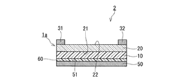
ヒータ1aを用いてヒータ付物品を作製できる。例えば、図3に示す通り、ヒータ付物品2は、成形体50と、粘着層60と、ヒータ1aとを備えている。成形体50は、被着面51を有する。成形体50は、金属材料又は合成樹脂で形成されている。粘着層60は、被着面51に接触している。接着層60は、例えば、アクリル系粘着剤等の公知の粘着剤によって形成されている。ヒータ1aは、粘着層60に接触しているともに粘着層60によって成形体50に取り付けられている。
An article with a heater can be manufactured using the
粘着層60は、例えば、ヒータ1aの基板10の透明導電性酸化物層20と接触している主面と反対側の主面に予め形成されていてもよい。この場合、粘着層60と被着面51とを対向させてヒータ1aを成形体50に押し付けることによって、ヒータ1aを成形体50に取り付けることができる。また、粘着層60はセパレータ(図示省略)によって覆われていてもよい。この場合、ヒータ1aを成形体50に取り付けるときに、セパレータが剥離されて粘着層60が露出する。セパレータ60は、例えば、ポリエチレンテレフタレート(PET)等のポリエステル樹脂製のフィルムである。
The
ヒータ1aは、例えば、近赤外線を用いた処理をなす装置において、この近赤外線の光路上に配置される。この装置は、例えば、近赤外線を用いて、センシング又は通信等の所定の処理を行う。成形体50は、例えば、このような装置の筐体を構成する。
The
以下、実施例により本発明をより詳細に説明する。なお、本発明は以下の実施例に限定されない。まず、実施例及び比較例に関する評価方法及び測定方法について説明する。 Hereinafter, the present invention will be described in more detail with reference to examples. Note that the present invention is not limited to the following embodiments. First, an evaluation method and a measurement method for Examples and Comparative Examples will be described.
[厚み測定]
X線回折装置(リガク社製、製品名:RINT2200)を用いて、X線反射率法によって、各実施例及び各比較例に係るヒータの透明導電性酸化物層(発熱体)の厚みを測定した。結果を表1に示す。また、X線回折装置を用いて、透明導電性酸化物層に対するX線回折パターンを得た。X線としてはCuKα線を用いた。各実施例において、得られたX線回折パターンから透明導電性酸化物層(発熱体)が多結晶構造であることが確認された。また、触針式表面形状測定器(ULVAC社製、製品名:Dektak8)を用いて、各実施例及び各比較例に係るヒータの給電用電極の端部の高さを計測して、各実施例及び各比較例に係るヒータの給電用電極の厚みを測定した。結果を表1に示す。
[Thickness measurement]
The thickness of the transparent conductive oxide layer (heating element) of the heater according to each example and each comparative example was measured by an X-ray reflectivity method using an X-ray diffractometer (manufactured by Rigaku Corporation, product name: RINT2200). did. Table 1 shows the results. Further, an X-ray diffraction pattern for the transparent conductive oxide layer was obtained using an X-ray diffraction apparatus. CuKα rays were used as X-rays. In each example, it was confirmed from the obtained X-ray diffraction pattern that the transparent conductive oxide layer (heating element) had a polycrystalline structure. The height of the end of the power supply electrode of the heater according to each example and each comparative example was measured using a stylus type surface shape measuring device (product name: Dektak8, manufactured by ULVAC), and The thickness of the power supply electrode of the heater according to the example and each comparative example was measured. Table 1 shows the results.
[シート抵抗、比抵抗、及び電気抵抗]
非接触式抵抗測定装置(ナプソン社製、製品名:NC−80MAP)を用いて、日本工業規格(JIS)Z 2316−1:2014に準拠して、渦電流測定法によって各実施例及び各比較例に係るヒータの透明導電性酸化物層(発熱体)のシート抵抗を測定した。結果を表1に示す。加えて、厚み測定により得られた透明導電性酸化物層(発熱体)の厚みと、透明導電性酸化物層(発熱体)のシート抵抗との積を求めて、各実施例及び各比較例に係るヒータの透明導電性酸化物層(発熱体)の比抵抗を決定した。結果を表1に示す。なお、表1における、給電用電極の比抵抗は文献又は仕様書の記載に基づいた値である。給電用電極の電極の寸法及び比抵抗から一対の給電用電極の長さ方向における電気抵抗の和(Re1+Re2)を求めた。結果を表2に示す。加えて、透明導電性酸化物層のシート抵抗と一対の給電用電極間の距離から一対の給電用電極の間における透明導電性酸化物層の電気抵抗RHを求めた。結果を表2に示す。
[Sheet resistance, specific resistance, and electric resistance]
Using a non-contact resistance measuring device (manufactured by Napson Corporation, product name: NC-80MAP), in accordance with Japanese Industrial Standards (JIS) Z2316-1: 2014, eddy current measurement method and each embodiment and each comparison The sheet resistance of the transparent conductive oxide layer (heating element) of the heater according to the example was measured. Table 1 shows the results. In addition, the product of the thickness of the transparent conductive oxide layer (heating element) obtained by the thickness measurement and the sheet resistance of the transparent conductive oxide layer (heating element) was determined, and each example and each comparative example were obtained. , The specific resistance of the transparent conductive oxide layer (heating element) of the heater was determined. Table 1 shows the results. Note that the specific resistance of the power supply electrode in Table 1 is a value based on the description in a literature or a specification. The sum (R e1 + R e2 ) of the electrical resistance in the length direction of the pair of power supply electrodes was determined from the dimensions and the specific resistance of the power supply electrode. Table 2 shows the results. In addition, the electrical resistance RH of the transparent conductive oxide layer between the pair of power supply electrodes was determined from the sheet resistance of the transparent conductive oxide layer and the distance between the pair of power supply electrodes. Table 2 shows the results.
[Hall効果測定]
Hall効果測定装置(東陽テクニカ社製、製品名:ResiTest 8400)を用いて、各実施例及び各比較例に係るヒータの透明導電性酸化物層(発熱体)について、van der Pauw法に従ってHall効果測定を行った。Hall効果測定の結果から、各実施例及び各比較例に係るヒータの透明導電性酸化物層(発熱体)のキャリア密度を求めた。結果を表1に示す。
[Hall effect measurement]
Using a Hall effect measuring device (manufactured by Toyo Technica Co., Ltd., product name: ResiTest 8400), the Hall effect was measured for the transparent conductive oxide layers (heating elements) of the heaters according to the examples and comparative examples according to the van der Pauw method. A measurement was made. From the results of the Hall effect measurement, the carrier densities of the transparent conductive oxide layers (heating elements) of the heaters according to the examples and the comparative examples were determined. Table 1 shows the results.
[ヒータ特性]
菊水電子工業社製の直流定電圧電源を用いて、各実施例及び各比較例に係るヒータの一対の給電用電極に12Vの電圧を印加して、ヒータの透明導電性酸化物層(発熱体)に電流を流す通電試験を行った。ヒータを電源に接続するための配線は、給電用電極の長さ方向における同一サイドの端部に取り付けた。通電試験の期間中に、フリアーシステムズ社製のサーモグラフィを用いて、透明導電性酸化物層(発熱体)の表面温度を測定し、昇温速度を算出した。面内の昇温速度の最高値及び最低値の結果を表2に示す。
[Heater characteristics]
Using a DC constant voltage power supply manufactured by Kikusui Electronics Co., Ltd., a voltage of 12 V was applied to a pair of power supply electrodes of the heaters according to each of the examples and the comparative examples, and a transparent conductive oxide layer (a heating element) of the heater was applied. ) Was conducted. The wiring for connecting the heater to the power supply was attached to the end of the same side in the length direction of the power supply electrode. During the period of the power-on test, the surface temperature of the transparent conductive oxide layer (heating element) was measured using a thermography manufactured by FLIR Systems, and the heating rate was calculated. Table 2 shows the results of the maximum and minimum values of the in-plane heating rate.
[耐クラック性]
透明導電性酸化物層が形成されたフィルムを2cm×10cmの矩形状に切り取り、耐クラック性を評価するための試験片を作製した。この試験片を長さ方向に直径25mmのステンレス製の丸棒に透明導電性酸化物層が外側になるように巻きつけ、試験片の両端に112.5gの重りを取り付け、重りを垂らした状態を30秒間保った。その後、透明導電性酸化物層におけるクラック発生の有無を目視により確認した。結果を表2に示す。
[Crack resistance]
The film on which the transparent conductive oxide layer was formed was cut into a rectangular shape of 2 cm × 10 cm to prepare a test piece for evaluating crack resistance. This test piece was wound around a stainless steel round bar having a diameter of 25 mm in the length direction so that the transparent conductive oxide layer was on the outside, and 112.5 g of weight was attached to both ends of the test piece, and the weight was hung. For 30 seconds. Thereafter, the presence or absence of cracks in the transparent conductive oxide layer was visually confirmed. Table 2 shows the results.
<実施例1>
100μmの厚みを有するポリエチレンナフタレート(PEN)のフィルム(帝人フィルムソリューション社製、製品名:テオネックス)の一方の主面上に、酸化インジウムスズ(ITO)(酸化スズの含有率:10重量%)をターゲット材として用いて、当該ターゲット材の表面での水平磁場の磁束密度が100mT(ミリテスラ)の高磁場であり、不活性ガスが存在する状態において、DCマグネトロンスパッタ法により、ITO膜を形成した。ITO膜を形成した後のPENフィルムを、150℃の大気中に3時間置いて、加熱アニール処理を行った。これにより、ITOを結晶化させ、透明導電性酸化物層を形成した。透明導電性酸化物層の厚みは50nmであった。
<Example 1>
On one main surface of a polyethylene naphthalate (PEN) film (manufactured by Teijin Film Solutions Ltd., product name: Teonex) having a thickness of 100 μm, indium tin oxide (ITO) (tin oxide content: 10% by weight) Was used as a target material, an ITO film was formed by DC magnetron sputtering in a state where the magnetic flux density of the horizontal magnetic field on the surface of the target material was a high magnetic field of 100 mT (millitesla) and an inert gas was present. . The PEN film after the formation of the ITO film was placed in the air at 150 ° C. for 3 hours to perform a heat annealing treatment. Thus, the ITO was crystallized to form a transparent conductive oxide layer. The thickness of the transparent conductive oxide layer was 50 nm.
次に、透明導電性酸化物層が形成されたPENフィルムを短冊状に切り出し、互いに対向して延びている透明導電性酸化物層の一対の端部が露出するようにマスキングフィルムで透明導電性酸化物層の一部を覆った。一対の端部のそれぞれは2mmの幅を有していた。この状態で、透明導電性酸化物層及びマスキングフィルムの上に、100nmの厚みを有するCu薄膜をDCマグネトロンスパッタ法により形成した。さらに、Cu薄膜に対して、湿式めっき処理を行い、Cu膜の厚みを20μmまで増加させた。その後、マスキングフィルムを除去して、透明導電性酸化物層の一対の端部に相当する部分に一対の給電用電極(第一給電用電極及び第二給電用電極)を形成した。このようにして、実施例1に係るヒータを得た。各給電用電極と透明導電性酸化物層との接触面の長さは60mmであり、一対の給電用電極間の距離は20mmであった。 Next, the PEN film on which the transparent conductive oxide layer is formed is cut into strips, and the transparent conductive oxide layer is exposed by a masking film so that a pair of ends of the transparent conductive oxide layer extending opposite to each other are exposed. Part of the oxide layer was covered. Each of the pair of ends had a width of 2 mm. In this state, a Cu thin film having a thickness of 100 nm was formed on the transparent conductive oxide layer and the masking film by DC magnetron sputtering. Further, the Cu thin film was subjected to wet plating to increase the thickness of the Cu film to 20 μm. Then, the masking film was removed, and a pair of power supply electrodes (a first power supply electrode and a second power supply electrode) were formed at portions corresponding to the pair of ends of the transparent conductive oxide layer. Thus, a heater according to Example 1 was obtained. The length of the contact surface between each power supply electrode and the transparent conductive oxide layer was 60 mm, and the distance between the pair of power supply electrodes was 20 mm.
<実施例2>
各給電用電極と透明導電性酸化物層との接触面の長さが100mmとなるように、透明導電性酸化物層が形成されたPENフィルムの切り出し及び給電用電極の作製の条件を調整した以外は、実施例1と同様にして実施例2に係るヒータを作製した。
<Example 2>
The conditions for cutting out the PEN film on which the transparent conductive oxide layer was formed and preparing the power supply electrode were adjusted so that the length of the contact surface between each power supply electrode and the transparent conductive oxide layer was 100 mm. Except for the above, a heater according to Example 2 was manufactured in the same manner as Example 1.
<実施例3>
各給電用電極と透明導電性酸化物層との接触面の長さが500mmとなるように、透明導電性酸化物層が形成されたPENフィルムの切り出し及び給電用電極の作製の条件を調整した以外は、実施例1と同様にして実施例3に係るヒータを作製した。
<Example 3>
The conditions for cutting out the PEN film on which the transparent conductive oxide layer was formed and for preparing the power supply electrode were adjusted so that the length of the contact surface between each power supply electrode and the transparent conductive oxide layer was 500 mm. Except for the above, a heater according to Example 3 was manufactured in the same manner as Example 1.
<実施例4>
下記の点以外は実施例1と同様にして実施例4に係るヒータを作製した。透明導電性酸化物層の厚みが200nmになるようにITO膜を形成するためのDCマグネトロンスパッタ法の条件を調整した。各給電用電極と透明導電性酸化物層との接触面の長さが100mmとなるように、かつ、一対の給電用電極間の距離が100mmとなるように透明導電性酸化物層が形成されたPENフィルムの切り出し及び給電用電極の作製の条件を調整した。
<Example 4>
A heater according to Example 4 was manufactured in the same manner as Example 1 except for the following points. The conditions of the DC magnetron sputtering method for forming the ITO film were adjusted so that the thickness of the transparent conductive oxide layer was 200 nm. The transparent conductive oxide layer is formed such that the length of the contact surface between each power supply electrode and the transparent conductive oxide layer is 100 mm, and the distance between the pair of power supply electrodes is 100 mm. The conditions for cutting out the PEN film and preparing the power supply electrode were adjusted.
<実施例5>
下記の点以外は実施例1と同様にして実施例5に係るヒータを作製した。透明導電性酸化物層の厚みが35nmになるようにITO膜を形成するためのDCマグネトロンスパッタ法の条件を調整した。各給電用電極と透明導電性酸化物層との接触面の長さが100mmとなるように、透明導電性酸化物層が形成されたPENフィルムの切り出し及び給電用電極の作製の条件を調整した。
<Example 5>
A heater according to Example 5 was manufactured in the same manner as Example 1 except for the following points. The conditions of the DC magnetron sputtering method for forming the ITO film were adjusted so that the thickness of the transparent conductive oxide layer became 35 nm. The conditions for cutting out the PEN film on which the transparent conductive oxide layer was formed and preparing the power supply electrode were adjusted so that the length of the contact surface between each power supply electrode and the transparent conductive oxide layer was 100 mm. .
<実施例6>
下記の点以外は実施例1と同様にして実施例6に係るヒータを作製した。透明導電性酸化物層の厚みが120nmになるようにITO膜を形成するためのDCマグネトロンスパッタ法の条件を調整した。各給電用電極と透明導電性酸化物層との接触面の長さが100mmとなるように、透明導電性酸化物層が形成されたPENフィルムの切り出し及び給電用電極の作製の条件を調整した。
<Example 6>
A heater according to Example 6 was manufactured in the same manner as Example 1 except for the following points. The conditions of the DC magnetron sputtering method for forming the ITO film were adjusted so that the thickness of the transparent conductive oxide layer became 120 nm. The conditions for cutting out the PEN film on which the transparent conductive oxide layer was formed and preparing the power supply electrode were adjusted so that the length of the contact surface between each power supply electrode and the transparent conductive oxide layer was 100 mm. .
<実施例7>
給電用電極がニッケル製となるように給電用電極の作製条件を調整した以外は、実施例2と同様にして実施例7に係るヒータを作製した。
<Example 7>
A heater according to Example 7 was manufactured in the same manner as in Example 2, except that the manufacturing conditions of the power supply electrode were adjusted so that the power supply electrode was made of nickel.
<実施例8>
給電用電極がSnPb(スズ鉛)合金となるように給電用電極の作製条件を調整した以外は、実施例2と同様にして実施例7に係るヒータを作製した。
<Example 8>
A heater according to Example 7 was manufactured in the same manner as in Example 2, except that the manufacturing conditions of the power supply electrode were adjusted such that the power supply electrode was made of a SnPb (tin-lead) alloy.
<実施例9>
給電用電極の厚みが2μmとなるように給電用電極の作製条件を調整した以外は、実施例2と同様にして実施例9に係るヒータを作製した。
<Example 9>
A heater according to Example 9 was manufactured in the same manner as in Example 2, except that the manufacturing conditions of the power supply electrode were adjusted so that the thickness of the power supply electrode was 2 μm.
<比較例1>
下記の点以外は、実施例1と同様にして比較例1に係るヒータを作製した。透明導電性酸化物層が形成されたPENフィルムを短冊状に切り出し、互いに対向して延びている透明導電性酸化物層の一対の端部に、銀粒子が分散しているペースト(藤倉化成社製、製品名:DOTITED-500)を塗布して固化させ、20μmの厚みを有する一対の給電用電極を形成した。各給電用電極と透明導電性酸化物層との接触面の長さは100mmであり、一対の給電用電極間の距離は20mmであった。
<Comparative Example 1>
Except for the following points, a heater according to Comparative Example 1 was manufactured in the same manner as in Example 1. A PEN film on which a transparent conductive oxide layer is formed is cut into strips, and a paste in which silver particles are dispersed at a pair of ends of the transparent conductive oxide layer extending opposite to each other (Fujikura Kasei Co., Ltd.) (Product name: DOTITED-500) was applied and solidified to form a pair of power supply electrodes having a thickness of 20 μm. The length of the contact surface between each power supply electrode and the transparent conductive oxide layer was 100 mm, and the distance between the pair of power supply electrodes was 20 mm.
<比較例2>
下記の点以外は、実施例1と同様にして比較例2に係るヒータを作製した。透明導電性酸化物層をなす材料(ITO)の比抵抗が8.0×10⁻⁴Ω・cmとなるように、透明導電性酸化物層の作製条件を調整した。具体的には、加熱アニール処理を行わずに、非晶質ITOで透明導電性酸化物層を形成した。加えて、各給電用電極と透明導電性酸化物層との接触面の長さが100mmとなるように、透明導電性酸化物層が形成されたPENフィルムの切り出し及び給電用電極の作製の条件を調整した。
<Comparative Example 2>
Except for the following, a heater according to Comparative Example 2 was produced in the same manner as in Example 1. The production conditions of the transparent conductive oxide layer were adjusted such that the specific resistance of the material (ITO) forming the transparent conductive oxide layer was 8.0 × 10 −4 Ω · cm. Specifically, a transparent conductive oxide layer was formed of amorphous ITO without performing the heat annealing treatment. In addition, conditions for cutting out the PEN film on which the transparent conductive oxide layer is formed and preparing the power supply electrode so that the length of the contact surface between each power supply electrode and the transparent conductive oxide layer is 100 mm. Was adjusted.
<比較例3>
下記の点以外は、比較例2と同様にして比較例3に係るヒータを作製した。透明導電性酸化物層の厚みが320nmになるようにDCマグネトロンスパッタ法の条件を調整した。なお、320nmの厚みを有する非晶質ITO膜を加熱アニール処理すると、カール及びクラックが生じ、使用可能なヒータを作製できなかった。
<Comparative Example 3>
Except for the following points, a heater according to Comparative Example 3 was produced in the same manner as in Comparative Example 2. The conditions of the DC magnetron sputtering method were adjusted such that the thickness of the transparent conductive oxide layer became 320 nm. In addition, when the amorphous ITO film having a thickness of 320 nm was subjected to heat annealing treatment, curling and cracks occurred, and a usable heater could not be manufactured.
表2に示す通り、実施例に係るヒータの通電試験の結果と、比較例1に係るヒータの通電試験の結果との対比より、(Re1+Re2)/RHが45%以下であることが発熱体における発熱量の空間的な偏りを抑制する観点から有利であることが示唆された。実施例に係るヒータの通電試験の結果と、比較例2に係るヒータの通電試験の結果との対比より、透明導電性酸化物層20をなす材料が1.4〜3.0×10-4Ω・cmの比抵抗を有することがヒータの発熱量を高める観点から有利であることが示唆された。実施例に係るヒータの通電試験の結果と、比較例3に係るヒータの通電試験の結果との対比より、透明導電性酸化物層20の厚みが20〜250nmの厚みを有することが、クラックの発生を防止する観点から有利であることが示唆された。
As shown in Table 2, ( Re1 + Re2 ) / RH is not more than 45% based on a comparison between the result of the power-on test of the heater according to the example and the result of the power-on test of the heater according to Comparative Example 1. It is suggested that is advantageous from the viewpoint of suppressing the spatial deviation of the calorific value in the heating element. From the comparison between the result of the power-on test of the heater according to the example and the result of the power-on test of the heater according to Comparative Example 2, the material of the transparent

1a、1b ヒータ
2 ヒータ付物品
10 基板
20 透明導電性酸化物層
21 第一主面
22 第二主面
31 第一給電用電極
32 第二給電用電極
50 成形体
51 被着面
60 粘着層
1a,
Claims (8)
前記基板上に配置された透明導電性酸化物層と、
前記透明導電性酸化物層に電気的に接続され、特定方向に延びている第一給電用電極と、
前記透明導電性酸化物層に電気的に接続され、前記第一給電用電極から離れて前記特定方向に延びている第二給電用電極と、を備え、
前記第一給電用電極と前記第二給電用電極との間における前記透明導電性酸化物層の電気抵抗に対する、前記第一給電用電極の前記特定方向における電気抵抗及び前記第二給電用電極の前記特定方向における電気抵抗の和の比が、45%以下であり、
前記透明導電性酸化物層は、20〜250nmの厚みを有し、かつ、1.4〜3.0×10⁻⁴Ω・cmの比抵抗を有する材料によって形成されている、
ヒータ。 Board and
A transparent conductive oxide layer disposed on the substrate,
A first power supply electrode electrically connected to the transparent conductive oxide layer and extending in a specific direction,
A second power supply electrode electrically connected to the transparent conductive oxide layer and extending in the specific direction away from the first power supply electrode,
For the electrical resistance of the transparent conductive oxide layer between the first power supply electrode and the second power supply electrode, the electrical resistance of the first power supply electrode in the specific direction and the second power supply electrode The ratio of the sum of the electrical resistances in the specific direction is 45% or less;
The transparent conductive oxide layer has a thickness of 20 to 250 nm and is formed of a material having a specific resistance of 1.4 to 3.0 × 10 −4 Ω · cm.
heater.
前記被着面に接触している粘着層と、
前記粘着層に接触しているともに前記粘着層によって前記成形体に取り付けられている、請求項1〜7のいずれか1項に記載のヒータと、を備えた、
ヒータ付物品。 A molded body having an adhered surface,
An adhesive layer in contact with the adherend surface,
The heater according to any one of claims 1 to 7, wherein the heater is in contact with the adhesive layer and attached to the molded body by the adhesive layer.
Articles with heater.
Priority Applications (7)
| Application Number | Priority Date | Filing Date | Title |
|---|---|---|---|
| JP2018145551A JP7162462B2 (en) | 2018-08-02 | 2018-08-02 | Heaters and articles with heaters |
| US17/260,313 US20210298129A1 (en) | 2018-08-02 | 2019-07-23 | Heater and article equipped with heater |
| CN201980051603.5A CN112534964A (en) | 2018-08-02 | 2019-07-23 | Heater and article with heater |
| EP19843585.1A EP3833156A4 (en) | 2018-08-02 | 2019-07-23 | Heater and article with heater |
| PCT/JP2019/028903 WO2020026898A1 (en) | 2018-08-02 | 2019-07-23 | Heater and article with heater |
| KR1020217003757A KR20210038571A (en) | 2018-08-02 | 2019-07-23 | Heater and heater attachment |
| TW108126556A TW202014045A (en) | 2018-08-02 | 2019-07-26 | Heater and article with heater |
Applications Claiming Priority (1)
| Application Number | Priority Date | Filing Date | Title |
|---|---|---|---|
| JP2018145551A JP7162462B2 (en) | 2018-08-02 | 2018-08-02 | Heaters and articles with heaters |
Publications (2)
| Publication Number | Publication Date |
|---|---|
| JP2020021663A true JP2020021663A (en) | 2020-02-06 |
| JP7162462B2 JP7162462B2 (en) | 2022-10-28 |
Family
ID=69231612
Family Applications (1)
| Application Number | Title | Priority Date | Filing Date |
|---|---|---|---|
| JP2018145551A Active JP7162462B2 (en) | 2018-08-02 | 2018-08-02 | Heaters and articles with heaters |
Country Status (7)
| Country | Link |
|---|---|
| US (1) | US20210298129A1 (en) |
| EP (1) | EP3833156A4 (en) |
| JP (1) | JP7162462B2 (en) |
| KR (1) | KR20210038571A (en) |
| CN (1) | CN112534964A (en) |
| TW (1) | TW202014045A (en) |
| WO (1) | WO2020026898A1 (en) |
Cited By (4)
| Publication number | Priority date | Publication date | Assignee | Title |
|---|---|---|---|---|
| JPWO2021187575A1 (en) * | 2020-03-19 | 2021-09-23 | ||
| JP2022055423A (en) * | 2020-09-29 | 2022-04-08 | 東海光学株式会社 | Electrical resistance setting method of heater glass, manufacturing method using the setting method, and heater glass manufactured using the manufacturing method |
| JP2022074708A (en) * | 2020-11-05 | 2022-05-18 | 日産自動車株式会社 | Transparent surface heater |
| US12156330B2 (en) | 2020-03-19 | 2024-11-26 | Nitto Denko Corporation | Light-transmitting electroconductive film and transparent electroconductive film |
Families Citing this family (1)
| Publication number | Priority date | Publication date | Assignee | Title |
|---|---|---|---|---|
| CN112383974B (en) * | 2020-11-11 | 2022-10-21 | 上海子誉电子陶瓷有限公司 | PTC electric heating element with one-side heating function |
Citations (6)
| Publication number | Priority date | Publication date | Assignee | Title |
|---|---|---|---|---|
| JPH03107123A (en) * | 1989-09-21 | 1991-05-07 | Canon Inc | panel heater |
| JPH04289685A (en) * | 1991-03-19 | 1992-10-14 | Teijin Ltd | Transparent sheet-like heater |
| JPH07153559A (en) * | 1993-12-02 | 1995-06-16 | Toyobo Co Ltd | Transparent sheet heater |
| JPH07335379A (en) * | 1994-06-10 | 1995-12-22 | Mitsui Toatsu Chem Inc | Transparent sheet heater and manufacturing method thereof |
| JP2005135692A (en) * | 2003-10-29 | 2005-05-26 | Kyocera Corp | Ceramic heater |
| JP2017091858A (en) * | 2015-11-12 | 2017-05-25 | 日東電工株式会社 | Amorphous transparent conductive film, crystalline transparent conductive film and method for producing the same |
Family Cites Families (9)
| Publication number | Priority date | Publication date | Assignee | Title |
|---|---|---|---|---|
| US4952783A (en) | 1989-03-20 | 1990-08-28 | W. H. Brady Co. | Light transmitting flexible film electrical heater panels |
| ATE117156T1 (en) * | 1990-11-21 | 1995-01-15 | Flex Products Inc | THIN-FILM CONDUCTIVE DEVICE AND METHOD FOR THE PRODUCTION THEREOF. |
| JP4952783B2 (en) | 2007-03-14 | 2012-06-13 | 富士通セミコンダクター株式会社 | Output circuit |
| JP5352878B2 (en) * | 2008-03-31 | 2013-11-27 | 公立大学法人高知工科大学 | Display substrate, method for manufacturing the same, and display device |
| JP5543907B2 (en) * | 2010-12-24 | 2014-07-09 | 日東電工株式会社 | Transparent conductive film and method for producing the same |
| JP5244950B2 (en) * | 2011-10-06 | 2013-07-24 | 日東電工株式会社 | Transparent conductive film |
| JP6316839B2 (en) * | 2012-12-20 | 2018-04-25 | サン−ゴバン グラス フランスSaint−Gobain Glass France | Glass plate provided with electric heating layer and method for producing the same |
| KR20150128004A (en) * | 2014-05-08 | 2015-11-18 | 울산대학교 산학협력단 | Preparing method for heating film of coating type and heating film of coating type prepared thereby |
| CN106416422B (en) * | 2014-09-04 | 2019-09-20 | 法国圣戈班玻璃厂 | Glass panels with electrically heated zones |
-
2018
- 2018-08-02 JP JP2018145551A patent/JP7162462B2/en active Active
-
2019
- 2019-07-23 EP EP19843585.1A patent/EP3833156A4/en active Pending
- 2019-07-23 WO PCT/JP2019/028903 patent/WO2020026898A1/en not_active Ceased
- 2019-07-23 CN CN201980051603.5A patent/CN112534964A/en active Pending
- 2019-07-23 KR KR1020217003757A patent/KR20210038571A/en not_active Withdrawn
- 2019-07-23 US US17/260,313 patent/US20210298129A1/en not_active Abandoned
- 2019-07-26 TW TW108126556A patent/TW202014045A/en unknown
Patent Citations (6)
| Publication number | Priority date | Publication date | Assignee | Title |
|---|---|---|---|---|
| JPH03107123A (en) * | 1989-09-21 | 1991-05-07 | Canon Inc | panel heater |
| JPH04289685A (en) * | 1991-03-19 | 1992-10-14 | Teijin Ltd | Transparent sheet-like heater |
| JPH07153559A (en) * | 1993-12-02 | 1995-06-16 | Toyobo Co Ltd | Transparent sheet heater |
| JPH07335379A (en) * | 1994-06-10 | 1995-12-22 | Mitsui Toatsu Chem Inc | Transparent sheet heater and manufacturing method thereof |
| JP2005135692A (en) * | 2003-10-29 | 2005-05-26 | Kyocera Corp | Ceramic heater |
| JP2017091858A (en) * | 2015-11-12 | 2017-05-25 | 日東電工株式会社 | Amorphous transparent conductive film, crystalline transparent conductive film and method for producing the same |
Cited By (5)
| Publication number | Priority date | Publication date | Assignee | Title |
|---|---|---|---|---|
| JPWO2021187575A1 (en) * | 2020-03-19 | 2021-09-23 | ||
| US12156330B2 (en) | 2020-03-19 | 2024-11-26 | Nitto Denko Corporation | Light-transmitting electroconductive film and transparent electroconductive film |
| JP2022055423A (en) * | 2020-09-29 | 2022-04-08 | 東海光学株式会社 | Electrical resistance setting method of heater glass, manufacturing method using the setting method, and heater glass manufactured using the manufacturing method |
| JP2022074708A (en) * | 2020-11-05 | 2022-05-18 | 日産自動車株式会社 | Transparent surface heater |
| JP7615619B2 (en) | 2020-11-05 | 2025-01-17 | 日産自動車株式会社 | Transparent Plane Heater |
Also Published As
| Publication number | Publication date |
|---|---|
| WO2020026898A1 (en) | 2020-02-06 |
| EP3833156A1 (en) | 2021-06-09 |
| TW202014045A (en) | 2020-04-01 |
| EP3833156A4 (en) | 2022-04-27 |
| KR20210038571A (en) | 2021-04-07 |
| JP7162462B2 (en) | 2022-10-28 |
| US20210298129A1 (en) | 2021-09-23 |
| CN112534964A (en) | 2021-03-19 |
Similar Documents
| Publication | Publication Date | Title |
|---|---|---|
| WO2020026898A1 (en) | Heater and article with heater | |
| JP6600550B2 (en) | Metal layer laminated transparent conductive film and touch sensor using the same | |
| US20110291968A1 (en) | Transparent electrically conductive substrate | |
| WO2012063524A1 (en) | Divided sputtering target and method for producing same | |
| EP3101517B1 (en) | Conductive substrate, conductive substrate laminate, method for producing conductive substrate, and method for producing conductive substrate laminate | |
| US11778699B2 (en) | Heater | |
| WO2013148967A1 (en) | Charge collection tape | |
| TW201706432A (en) | Laminated wiring film for electronic components and sputtering target material for forming coating layer | |
| JP2020167047A (en) | heater | |
| EP3852491A1 (en) | Heater and article with heater | |
| JP2011227999A (en) | Planar heating element | |
| TW201446981A (en) | Touch panel, preparing method thereof, and Ag-Pd-Nd alloy for touch panel | |
| TWI274523B (en) | Heating apparatus of thermal electric type touch control apparatus | |
| JP7162461B2 (en) | Heater member, heater tape, and molded body with heater member | |
| JP5565764B2 (en) | Electromagnetic wave interference prevention transfer film | |
| TWI706299B (en) | Conductive substrate, manufacturing method of conductive substrate | |
| JP7176879B2 (en) | heater | |
| JP2020167106A (en) | heater | |
| JP2021096994A (en) | heater |
Legal Events
| Date | Code | Title | Description |
|---|---|---|---|
| A621 | Written request for application examination |
Free format text: JAPANESE INTERMEDIATE CODE: A621 Effective date: 20210527 |
|
| A131 | Notification of reasons for refusal |
Free format text: JAPANESE INTERMEDIATE CODE: A131 Effective date: 20220628 |
|
| A521 | Request for written amendment filed |
Free format text: JAPANESE INTERMEDIATE CODE: A523 Effective date: 20220819 |
|
| TRDD | Decision of grant or rejection written | ||
| A01 | Written decision to grant a patent or to grant a registration (utility model) |
Free format text: JAPANESE INTERMEDIATE CODE: A01 Effective date: 20221004 |
|
| A61 | First payment of annual fees (during grant procedure) |
Free format text: JAPANESE INTERMEDIATE CODE: A61 Effective date: 20221018 |
|
| R150 | Certificate of patent or registration of utility model |
Ref document number: 7162462 Country of ref document: JP Free format text: JAPANESE INTERMEDIATE CODE: R150 |
|
| R250 | Receipt of annual fees |
Free format text: JAPANESE INTERMEDIATE CODE: R250 |