JP2020003601A - Display - Google Patents
Display Download PDFInfo
- Publication number
- JP2020003601A JP2020003601A JP2018121866A JP2018121866A JP2020003601A JP 2020003601 A JP2020003601 A JP 2020003601A JP 2018121866 A JP2018121866 A JP 2018121866A JP 2018121866 A JP2018121866 A JP 2018121866A JP 2020003601 A JP2020003601 A JP 2020003601A
- Authority
- JP
- Japan
- Prior art keywords
- substrate
- area
- main surface
- display
- spacers
- Prior art date
- Legal status (The legal status is an assumption and is not a legal conclusion. Google has not performed a legal analysis and makes no representation as to the accuracy of the status listed.)
- Pending
Links
Images


Classifications
-
- G—PHYSICS
- G02—OPTICS
- G02F—OPTICAL DEVICES OR ARRANGEMENTS FOR THE CONTROL OF LIGHT BY MODIFICATION OF THE OPTICAL PROPERTIES OF THE MEDIA OF THE ELEMENTS INVOLVED THEREIN; NON-LINEAR OPTICS; FREQUENCY-CHANGING OF LIGHT; OPTICAL LOGIC ELEMENTS; OPTICAL ANALOGUE/DIGITAL CONVERTERS
- G02F1/00—Devices or arrangements for the control of the intensity, colour, phase, polarisation or direction of light arriving from an independent light source, e.g. switching, gating or modulating; Non-linear optics
- G02F1/01—Devices or arrangements for the control of the intensity, colour, phase, polarisation or direction of light arriving from an independent light source, e.g. switching, gating or modulating; Non-linear optics for the control of the intensity, phase, polarisation or colour
- G02F1/13—Devices or arrangements for the control of the intensity, colour, phase, polarisation or direction of light arriving from an independent light source, e.g. switching, gating or modulating; Non-linear optics for the control of the intensity, phase, polarisation or colour based on liquid crystals, e.g. single liquid crystal display cells
- G02F1/133—Constructional arrangements; Operation of liquid crystal cells; Circuit arrangements
- G02F1/1333—Constructional arrangements; Manufacturing methods
- G02F1/1339—Gaskets; Spacers; Sealing of cells
-
- G—PHYSICS
- G09—EDUCATION; CRYPTOGRAPHY; DISPLAY; ADVERTISING; SEALS
- G09F—DISPLAYING; ADVERTISING; SIGNS; LABELS OR NAME-PLATES; SEALS
- G09F9/00—Indicating arrangements for variable information in which the information is built-up on a support by selection or combination of individual elements
- G09F9/30—Indicating arrangements for variable information in which the information is built-up on a support by selection or combination of individual elements in which the desired character or characters are formed by combining individual elements
Abstract
Description
本発明の実施形態は、表示装置に関する。 Embodiments of the present invention relate to a display device.
一般に、表示装置として液晶表示装置などが知られている。例えば、液晶表示装置は、液晶表示パネルと、照明装置と、を備えている。液晶表示パネルは、表示領域と、表示領域を囲む非表示領域と、を備えている。ところで、表示装置としては、信頼性の高い表示装置が求められている。 Generally, a liquid crystal display device or the like is known as a display device. For example, a liquid crystal display device includes a liquid crystal display panel and a lighting device. The liquid crystal display panel includes a display area and a non-display area surrounding the display area. By the way, a highly reliable display device is required as a display device.
本実施形態は、信頼性の高い表示装置を提供する。 This embodiment provides a highly reliable display device.
一実施形態に係る表示装置は、
第1主面及び前記第1主面とは反対側の第2主面を含み、表示領域及び前記表示領域の外側の非表示領域に位置した第1基板と、前記第2主面に隙間を置いて対向した第3主面及び前記第3主面とは反対側の第4主面とを含み、前記表示領域及び前記非表示領域に位置した第2基板と、前記非表示領域に位置し、前記第1基板と前記第2基板とを接合したシール材と、前記第1基板、前記第2基板、及び前記シール材で囲まれた空間に設けられた液晶層と、を有する表示セルを備え、前記非表示領域は、第1領域を含む周辺領域と、前記表示領域及び前記周辺領域の間に位置し前記表示領域を囲む額縁領域と、を有し、前記シール材と前記液晶層との境界は、前記額縁領域に位置し、前記第1主面から前記第4主面までの距離を第1距離とすると、前記額縁領域の前記第1距離は、前記表示領域の前記第1距離と、同一であり、前記周辺領域の前記第1距離うち少なくとも前記第1領域の前記第1距離は、前記表示領域の前記第1距離より短い。
The display device according to one embodiment includes:
A first substrate including a first main surface and a second main surface opposite to the first main surface, the first substrate being located in a display region and a non-display region outside the display region; A second substrate positioned in the display area and the non-display area, and a third substrate positioned in the non-display area; A display material comprising: a sealing material that joins the first substrate and the second substrate; and a liquid crystal layer provided in a space surrounded by the first substrate, the second substrate, and the sealing material. Wherein the non-display area has a peripheral area including a first area, and a frame area located between the display area and the peripheral area and surrounding the display area, wherein the sealant and the liquid crystal layer Is located in the frame area, and a distance from the first main surface to the fourth main surface is defined as a first distance. And the first distance of the frame area is the same as the first distance of the display area, and at least the first distance of the first area of the first distance of the peripheral area is the display area. Is shorter than the first distance.
以下に、本発明の実施形態、及び変形例について、図面を参照しつつ説明する。なお、開示はあくまで一例にすぎず、当業者において、発明の主旨を保っての適宜変更について容易に想到し得るものについては、当然に本発明の範囲に含有されるものである。また、図面は説明をより明確にするため、実際の態様に比べ、各部の幅、厚さ、形状等について模式的に表される場合があるが、あくまで一例であって、本発明の解釈を限定するものではない。また、本明細書と各図において、既出の図に関して前述したものと同様の要素には、同一の符号を付して、詳細な説明を適宜省略することがある。 Hereinafter, embodiments and modifications of the present invention will be described with reference to the drawings. It should be noted that the disclosure is merely an example, and those skilled in the art can easily conceive of appropriate modifications while maintaining the gist of the invention, which are naturally included in the scope of the present invention. In addition, in order to make the description clearer, the width, thickness, shape, and the like of each part may be schematically illustrated as compared with actual embodiments, but this is merely an example, and the interpretation of the present invention is not limited thereto. There is no limitation. In the specification and the drawings, components similar to those described in regard to a drawing thereinabove are marked with like reference numerals, and a detailed description is omitted as appropriate.
(一実施形態)
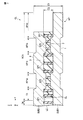
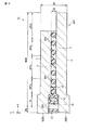
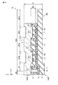
まず、一実施形態に係る表示装置について説明する。図1は、一実施形態に係る表示装置DSPを示す斜視図である。図2は、表示装置DSPを示す他の斜視図である。図3は、表示装置DSPの照明装置ILを示す斜視図である。
(One embodiment)
First, a display device according to an embodiment will be described. FIG. 1 is a perspective view showing a display device DSP according to one embodiment. FIG. 2 is another perspective view showing the display device DSP. FIG. 3 is a perspective view showing the illumination device IL of the display device DSP.
図1乃至図3に示すように、第1方向X、第2方向Y、及び第3方向Zは、互いに直交しているが、90度以外の角度で交差していてもよい。第1方向X及び第2方向Yは、表示装置DSPを構成する基板の主面と平行な方向に相当し、第3方向Zは、表示装置DSPの厚さ方向に相当する。以下の説明において、第3方向Zを示す矢印の先端に向かう方向を「上」と称し、矢印の先端から逆に向かう方向を「下」と称する。「第1部材の上の第2部材」及び「第1部材の下の第2部材」とした場合、第2部材は、第1部材に接していてもよいし、第1部材から離れて位置していてもよい。また、第3方向Zを示す矢印の先端側から第1方向X及び第2方向Yによって規定されるX−Y平面をみることを平面視という。 As shown in FIGS. 1 to 3, the first direction X, the second direction Y, and the third direction Z are orthogonal to each other, but may intersect at an angle other than 90 degrees. The first direction X and the second direction Y correspond to directions parallel to the main surface of the substrate constituting the display device DSP, and the third direction Z corresponds to the thickness direction of the display device DSP. In the following description, the direction toward the tip of the arrow indicating the third direction Z is referred to as “up”, and the direction from the tip of the arrow to the opposite direction is referred to as “down”. In the case of “the second member above the first member” and “the second member below the first member”, the second member may be in contact with the first member or may be located away from the first member. It may be. Viewing the XY plane defined by the first direction X and the second direction Y from the tip side of the arrow indicating the third direction Z is referred to as plan view.
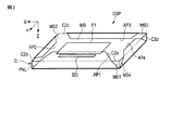
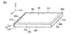
表示装置DSPは、照明装置IL、表示パネルPNL、第1ドライバとしての駆動IC DD、配線基板F1などを備えている。表示パネルPNLは、表示領域DAと、表示領域DAの外側の非表示領域NDAと、を備えている。照明装置ILは、板状の形状を有している。照明装置ILは、少なくとも表示パネルPNLの表示領域DAに光を放出するように構成されている。照明装置ILは、上面MUと、第1側面MS1と、上面MU及び第1側面MS1の間にて直線状に延在する第1角部C1aと、を含んでいる。 The display device DSP includes a lighting device IL, a display panel PNL, a driving IC DD as a first driver, a wiring board F1, and the like. The display panel PNL includes a display area DA and a non-display area NDA outside the display area DA. The lighting device IL has a plate-like shape. The illumination device IL is configured to emit light to at least the display area DA of the display panel PNL. The illumination device IL includes an upper surface MU, a first side surface MS1, and a first corner C1a extending linearly between the upper surface MU and the first side surface MS1.
本実施形態において、照明装置ILは、上面MUの反対側の下面MBと、第1側面MS1から連続して設けられた第2側面MS2と、第1側面MS1の反対側の第3側面MS3と、第2側面MS2の反対側の第4側面MS4と、をさらに含んでいる。第1側面MS1、第2側面MS2、第3側面MS3、及び第4側面MS4は、長方形の形状を有している。上面MU、及び下面MBは、四角形として、例えば長方形の形状を有している。上面MU、及び下面MBの各々は、第1方向Xに延在する一対の長辺と、第2方向Yに延在する一対の短辺と、を有している。 In the present embodiment, the lighting device IL includes a lower surface MB opposite to the upper surface MU, a second side surface MS2 provided continuously from the first side surface MS1, and a third side surface MS3 opposite to the first side surface MS1. , A fourth side surface MS4 opposite to the second side surface MS2. The first side surface MS1, the second side surface MS2, the third side surface MS3, and the fourth side surface MS4 have a rectangular shape. The upper surface MU and the lower surface MB have, for example, a rectangular shape as a square. Each of the upper surface MU and the lower surface MB has a pair of long sides extending in the first direction X and a pair of short sides extending in the second direction Y.
さらに、照明装置ILは、上面MU及び第2側面MS2の間にて直線状に延在する第1角部C1bと、上面MU及び第3側面MS3の間にて直線状に延在する第1角部C1cと、上面MU及び第4側面MS4の間にて直線状に延在する第1角部C1dと、第1側面MS1及び下面MBの間にて直線状に延在する第2角部C2aと、第2側面MS2及び下面MBの間にて直線状に延在する第2角部C2bと、第3側面MS3及び下面MBの間にて直線状に延在する第2角部C2cと、第4側面MS4及び下面MBの間にて直線状に延在する第2角部C2dと、を含んでいる。第1角部C1a,C1c及び第2角部C2a,C2cは第1方向Xに延在し、第1角部C1b,C1d及び第2角部C2b,C2dは第2方向Yに延在している。 Further, the illumination device IL includes a first corner C1b linearly extending between the upper surface MU and the second side surface MS2, and a first corner C1b linearly extending between the upper surface MU and the third side surface MS3. A corner C1c, a first corner C1d extending linearly between the upper surface MU and the fourth side surface MS4, and a second corner extending linearly between the first side surface MS1 and the lower surface MB. C2a, a second corner portion C2b extending linearly between the second side surface MS2 and the lower surface MB, and a second corner portion C2c extending linearly between the third side surface MS3 and the lower surface MB. , A second corner C2d extending linearly between the fourth side surface MS4 and the lower surface MB. The first corners C1a, C1c and the second corners C2a, C2c extend in the first direction X, and the first corners C1b, C1d and the second corners C2b, C2d extend in the second direction Y. I have.
照明装置ILは、導光体LGと、導光体LGに向けて光を出射する光源ユニットLUと、を備えている。この例では、光源ユニットLUが第4側面MS4を有している。導光体LGは、少なくとも表示領域DAに位置した導光板を備えている。例えば、導光体LGは、導光板と、第1側面MS1、第2側面MS2、及び第3側面MS3を有するフレーム部と、下面MBを有する光反射板と、を有している。この場合、上記フレーム部及び上記光反射板は、光源ユニットLUとともに上記導光板を囲んでいる。フレーム部は、上記光反射板と同様、上記導光板側の面が光反射性を有していてもよい。 The illumination device IL includes a light guide LG and a light source unit LU that emits light toward the light guide LG. In this example, the light source unit LU has a fourth side surface MS4. The light guide LG includes a light guide plate located at least in the display area DA. For example, the light guide LG includes a light guide plate, a frame portion having a first side surface MS1, a second side surface MS2, and a third side surface MS3, and a light reflection plate having a lower surface MB. In this case, the frame portion and the light reflection plate surround the light guide plate together with the light source unit LU. The surface of the frame portion on the light guide plate side may have light reflectivity similarly to the light reflection plate.
但し、照明装置ILの構成は、上記の構成に限定されるものではなく、種々変形可能である。例えば、照明装置ILは、上記フレーム部及び上記光反射板無しに形成されてもよい。また、上記導光板が、第1側面MS1、第2側面MS2、第3側面MS3、及び下面MBなどを有していてもよい。 However, the configuration of the illumination device IL is not limited to the above configuration, and can be variously modified. For example, the illumination device IL may be formed without the frame portion and the light reflection plate. Further, the light guide plate may have a first side surface MS1, a second side surface MS2, a third side surface MS3, a lower surface MB, and the like.
表示パネルPNLの表示領域DAは、照明装置ILの上面MUと対向している。表示パネルPNLの非表示領域NDAは、照明装置ILに沿って折り曲げられ、上面MU、第1側面MS1、第2側面MS2、第3側面MS3、第4側面MS4、及び下面MBと対向している。駆動IC DD、及び配線基板F1は、下面MBと対向している。下面MBと対向する側において、駆動IC DDは表示パネルPNLの非表示領域NDAに搭載され、配線基板F1は表示パネルPNLの非表示領域NDAに接続されている。 The display area DA of the display panel PNL faces the upper surface MU of the lighting device IL. The non-display area NDA of the display panel PNL is bent along the illumination device IL, and faces the upper surface MU, the first side surface MS1, the second side surface MS2, the third side surface MS3, the fourth side surface MS4, and the lower surface MB. . The drive IC DD and the wiring board F1 face the lower surface MB. On the side facing the lower surface MB, the drive IC DD is mounted on the non-display area NDA of the display panel PNL, and the wiring board F1 is connected to the non-display area NDA of the display panel PNL.
表示パネルPNLの非表示領域NDAは、額縁領域FAと、周辺領域APと、を有している。額縁領域FAは、表示領域DA及び周辺領域APの間に位置し、表示領域DAを囲み、照明装置ILの上面MUと対向している。本実施形態において、表示パネルPNLの非表示領域NDAは、互いに独立して延出した4つの周辺領域AP1,AP2,AP3,AP4を有している。各々の周辺領域AP1,AP2,AP3,AP4は、照明装置ILのうち対応する1つの側面MSと、下面MBと、対向している。但し、周辺領域AP2,AP3,AP4の各々の延出量(長さ)は、図2に示す例より短くともよい。この場合、周辺領域AP2,AP3,AP4の各々は、照明装置ILのうち対応する1つの側面MSと対向していればよく、下面MBと対向していなくともよい。 The non-display area NDA of the display panel PNL has a frame area FA and a peripheral area AP. The frame area FA is located between the display area DA and the peripheral area AP, surrounds the display area DA, and faces the upper surface MU of the lighting device IL. In the present embodiment, the non-display area NDA of the display panel PNL has four peripheral areas AP1, AP2, AP3, and AP4 extending independently of each other. Each of the peripheral regions AP1, AP2, AP3, and AP4 faces one corresponding side surface MS and the lower surface MB of the lighting device IL. However, the extension amount (length) of each of the peripheral regions AP2, AP3, and AP4 may be shorter than the example shown in FIG. In this case, each of the peripheral areas AP2, AP3, and AP4 only needs to face one corresponding side surface MS of the illumination device IL, and does not have to face the lower surface MB.
図4は、表示装置DSPの表示パネルPNL、駆動IC DD、及び配線基板F1を展開して示す平面図である。
図4に示すように、表示パネルPNLは、画像を表示する表示セルCLを有している。表示セルCLは、第1基板SUB1と、第2基板SUB2と、を有している。駆動IC DDは第1基板SUB1に搭載され、配線基板F1は第1基板SUB1に連結されている。第2基板SUB2は、駆動IC DD及び配線基板F1のための領域を除き、第1基板SUB1に重ねられている。本実施形態において、表示セルCLは、平面視にて八角形の形状を有している。
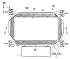
FIG. 4 is an exploded plan view showing the display panel PNL, the driving IC DD, and the wiring board F1 of the display device DSP.
As shown in FIG. 4, the display panel PNL has a display cell CL for displaying an image. The display cell CL has a first substrate SUB1 and a second substrate SUB2. The driving IC DD is mounted on the first substrate SUB1, and the wiring substrate F1 is connected to the first substrate SUB1. The second substrate SUB2 is overlaid on the first substrate SUB1 except for a region for the drive IC DD and the wiring substrate F1. In the present embodiment, the display cell CL has an octagonal shape in plan view.
表示セルCLは、表示領域DA、額縁領域FA、及び周辺領域AP1,AP2,AP3,AP4を含んでいる。周辺領域AP1は、第1領域AP1a、第2領域AP1b、第3領域AP1c、及び第4領域AP1dを含んでいる。同様に、周辺領域AP2,AP3,AP4も、第1乃至第4領域を含んでいる。第1領域に対応する符号の末尾にはaを付し、第2領域に対応する符号の末尾にはbを付し、第3領域に対応する符号の末尾にはcを付し、第4領域に対応する符号の末尾にはdを付している。また、図中、第1及び第3領域には、斜線を付している。なお、駆動IC DDは周辺領域AP1の第4領域AP1dに位置し、配線基板F1は第4領域AP1dに物理的に固定されている。 The display cell CL includes a display area DA, a frame area FA, and peripheral areas AP1, AP2, AP3, and AP4. The peripheral area AP1 includes a first area AP1a, a second area AP1b, a third area AP1c, and a fourth area AP1d. Similarly, the peripheral areas AP2, AP3, and AP4 also include first to fourth areas. The code corresponding to the first area is suffixed with a, the code corresponding to the second area is suffixed with b, the code corresponding to the third area is suffixed with c, The symbol “d” is added to the end of the code corresponding to the area. In the figure, the first and third regions are hatched. Note that the driving IC DD is located in the fourth area AP1d of the peripheral area AP1, and the wiring board F1 is physically fixed to the fourth area AP1d.
各々の周辺領域AP1,AP2,AP3,AP4において、第1乃至第4領域は、額縁領域FA側から順に並んでいる。周辺領域AP1,AP3において、第1乃至第4領域は、第2方向Yに並べられている。周辺領域AP2,AP4において、第1乃至第4領域は、第1方向Xに並べられている。 In each of the peripheral areas AP1, AP2, AP3, and AP4, the first to fourth areas are arranged in order from the frame area FA side. In the peripheral areas AP1 and AP3, the first to fourth areas are arranged in the second direction Y. In the peripheral areas AP2 and AP4, the first to fourth areas are arranged in the first direction X.
周辺領域AP1において、第1領域AP1aは上記第1角部C1aに沿って(第1方向Xに)延在し、第3領域AP1cは上記第2角部C2aに沿って(第1方向Xに)延在している。周辺領域AP2において、第1領域AP2aは上記第1角部C1bに沿って(第2方向Yに)延在し、第3領域AP2cは上記第2角部C2bに沿って(第2方向Yに)延在している。周辺領域AP3において、第1領域AP3aは上記第1角部C1cに沿って(第1方向Xに)延在し、第3領域AP3cは上記第2角部C2cに沿って(第1方向Xに)延在している。周辺領域AP4において、第1領域AP4aは上記第1角部C1dに沿って(第2方向Yに)延在し、第3領域AP4cは上記第2角部C2dに沿って(第2方向Yに)延在している。 In the peripheral area AP1, the first area AP1a extends along the first corner C1a (in the first direction X), and the third area AP1c extends along the second corner C2a (in the first direction X). ) Extending. In the peripheral area AP2, the first area AP2a extends along the first corner C1b (in the second direction Y), and the third area AP2c extends along the second corner C2b (in the second direction Y). ) Extending. In the peripheral area AP3, the first area AP3a extends along the first corner C1c (in the first direction X), and the third area AP3c extends along the second corner C2c (in the first direction X). ) Extending. In the peripheral area AP4, the first area AP4a extends along the first corner C1d (in the second direction Y), and the third area AP4c extends along the second corner C2d (in the second direction Y). ) Extending.
図5は、表示セルCL、及び駆動IC DDを示す回路図であり、一画素PXの回路構成を併せて示す図である。なお、ここでは、回路図の一例を示すものであり、図5に示す回路図に限定されるものではない。
図5に示すように、表示セルCLは、表示領域DAにおいて、複数の画素PXと、複数本の走査線G(G1〜Gn)と、複数本の信号線S(S1〜Sm)と、共通電極CEと、を備えている。複数の画素PXは、第1方向X及び第2方向Yにマトリクス状に配置されている。表示領域DAにおいて、走査線Gの各々は第1方向Xに延出し、信号線Sの各々は第2方向Yに延出している。非表示領域NDAにおいて、表示セルCLは、第2ドライバとしての走査線駆動回路GDと、第3ドライバとしての信号線駆動回路SDと、を有している。走査線Gの各々は、非表示領域NDAに延出し、走査線駆動回路GDに接続されている。なお、本実施形態と異なり、走査線駆動回路GDは、周辺領域AP4にも設けられていてもよく、2つの走査線駆動回路GDを用いて複数の走査線Gを駆動してもよい。信号線Sの各々は、非表示領域NDAに延出し、信号線駆動回路SDに接続されている。共通電極CEは、複数の画素PXで共用されている。
FIG. 5 is a circuit diagram showing the display cell CL and the driving IC DD, and also shows a circuit configuration of one pixel PX. Note that, here, an example of a circuit diagram is shown, and the circuit diagram is not limited to the circuit diagram shown in FIG.
As shown in FIG. 5, the display cell CL has a plurality of pixels PX, a plurality of scanning lines G (G1 to Gn), and a plurality of signal lines S (S1 to Sm) in the display area DA. And an electrode CE. The plurality of pixels PX are arranged in a matrix in the first direction X and the second direction Y. In the display area DA, each of the scanning lines G extends in the first direction X, and each of the signal lines S extends in the second direction Y. In the non-display area NDA, the display cell CL has a scanning line driving circuit GD as a second driver and a signal line driving circuit SD as a third driver. Each of the scanning lines G extends to the non-display area NDA and is connected to the scanning line driving circuit GD. Note that, unlike the present embodiment, the scanning line driving circuit GD may be provided also in the peripheral area AP4, and may drive a plurality of scanning lines G using two scanning line driving circuits GD. Each of the signal lines S extends to the non-display area NDA and is connected to the signal line driving circuit SD. The common electrode CE is shared by a plurality of pixels PX.
走査線駆動回路GD、信号線駆動回路SD、及び共通電極CEは、駆動IC DDに電気的に接続されている。なお、本実施形態と異なり、信号線駆動回路SDは、駆動IC DDから独立することなく、駆動IC DD内に組み込まれていてもよい。駆動IC DDは、表示セルCLのアウタリードボンディング(Outer Lead Bonding)のパッド群(OLBパッド群)PGに電気的に接続されている。なお、配線基板F1は、OLBパッド群PGに電気的に接続される。 The scanning line driving circuit GD, the signal line driving circuit SD, and the common electrode CE are electrically connected to the driving IC DD. Note that, unlike the present embodiment, the signal line drive circuit SD may be incorporated in the drive IC DD without being independent from the drive IC DD. The drive IC DD is electrically connected to a pad group (OLB pad group) PG of outer lead bonding (Outer Lead Bonding) of the display cell CL. Note that the wiring board F1 is electrically connected to the OLB pad group PG.
各画素PXは、スイッチング素子SW、画素電極PE、共通電極CE、液晶層LCなどを備えている。スイッチング素子SWは、例えば薄膜トランジスタ(TFT)によって構成され、走査線G及び信号線Sと電気的に接続されている。画素電極PEは、スイッチング素子SWと電気的に接続されている。各画素PXの画素電極PEは、それぞれ共通電極CEと対向している。液晶層LCは、画素電極PEと共通電極CEとの間に生じる電界によって駆動される。画素電極PEには、保持容量CSが結合されている。保持容量CSは、例えば、共通電極CEと同電位の電極と、画素電極PEと同電位の電極と、の間に形成されている。上記のことから、本実施形態の表示セルCLは液晶表示セルであり、表示パネルPNLは液晶表示パネルであり、表示装置DSPは液晶表示装置である。 Each pixel PX includes a switching element SW, a pixel electrode PE, a common electrode CE, a liquid crystal layer LC, and the like. The switching element SW is composed of, for example, a thin film transistor (TFT), and is electrically connected to the scanning line G and the signal line S. The pixel electrode PE is electrically connected to the switching element SW. The pixel electrode PE of each pixel PX faces the common electrode CE. The liquid crystal layer LC is driven by an electric field generated between the pixel electrode PE and the common electrode CE. The storage capacitor CS is coupled to the pixel electrode PE. The storage capacitor CS is formed, for example, between an electrode having the same potential as the common electrode CE and an electrode having the same potential as the pixel electrode PE. From the above, the display cell CL of the present embodiment is a liquid crystal display cell, the display panel PNL is a liquid crystal display panel, and the display device DSP is a liquid crystal display device.
ここでは画素PXの詳細な構成についての説明を省略するが、画素PXは、上記第1基板SUB1の主面の法線に沿った縦電界を利用する表示モード、第1基板SUB1の主面に対して斜め方向に傾斜した斜め電界を利用する表示モード、第1基板SUB1の主面に沿った横電界を利用する表示モード、さらには、上記の縦電界、横電界、及び斜め電界を適宜組み合わせて利用する表示モードのいずれも適用可能である。ここで言う第1基板SUB1の主面とは、第1方向X及び第2方向Yで規定されるX−Y平面と平行な面である。 Although a detailed description of the configuration of the pixel PX is omitted here, the pixel PX is provided in a display mode using a vertical electric field along a normal line of the main surface of the first substrate SUB1. In contrast, a display mode using an oblique electric field inclined in an oblique direction, a display mode using a horizontal electric field along the main surface of the first substrate SUB1, and a combination of the vertical electric field, the horizontal electric field, and the oblique electric field are appropriately combined. Any of the display modes that are used by the user can be applied. Here, the main surface of the first substrate SUB1 is a surface parallel to the XY plane defined by the first direction X and the second direction Y.
図6は、図4の線VI−VIに沿った表示パネルPNLを示す断面図である。
図6に示すように、表示セルCLは、第1基板SUB1と、第2基板SUB2と、シール材SLと、液晶層LCと、を備えている。第1基板SUB1は、第1主面1及び第1主面とは反対側の第2主面2を含み、表示領域DA及び非表示領域NDAに位置している。第2基板SUB2は、第1基板SUB1に所定の隙間を置いて対向配置されている。第2基板SUB2は、第2主面2に隙間を置いて対向した第3主面3及び第3主面とは反対側の第4主面4とを含み、表示領域DA及び非表示領域NDAに位置している。第2基板SUB2は、非表示領域NDAにて遮光層LSを有している。シール材SLは、第1基板SUB1と第2基板SUB2との間に設けられ、非表示領域NDAに位置し、表示領域DAを囲み、第1基板SUB1と第2基板SUB2とを接合している。液晶層LCは、第1基板SUB1、第2基板SUB2、及びシール材SLで囲まれた空間に設けられている。シール材SLと液晶層LCとの境界は、額縁領域FAに位置している。
FIG. 6 is a sectional view showing the display panel PNL along the line VI-VI in FIG.
As shown in FIG. 6, the display cell CL includes a first substrate SUB1, a second substrate SUB2, a sealing material SL, and a liquid crystal layer LC. The first substrate SUB1 includes a first
表示パネルPNLは、表示セルCLに加えて、第1光学フィルムOF1と、第2光学フィルムOF2と、表示セルCLと第1光学フィルムOF1との間に介在する接着層AD1と、表示セルCLと第2光学フィルムOF2との間に介在する接着層AD2と、を備えている。 The display panel PNL includes, in addition to the display cell CL, a first optical film OF1, a second optical film OF2, an adhesive layer AD1 interposed between the display cell CL and the first optical film OF1, and a display cell CL. And an adhesive layer AD2 interposed between the second optical film OF2.
第1光学フィルムOF1は、第1偏光板PL1を含み、接着層AD1により第1基板SUB1に接着されている。第2光学フィルムOF2は、第2偏光板PL2を含み、接着層AD2により第2基板SUB2に接着されている。本実施形態と異なり、第1光学フィルムOF1及び第2光学フィルムOF2は、偏光板PLだけではなく、位相差板などの他の光学機能層を含んでいてもよい。 The first optical film OF1 includes a first polarizing plate PL1, and is bonded to the first substrate SUB1 by an adhesive layer AD1. The second optical film OF2 includes a second polarizing plate PL2, and is bonded to the second substrate SUB2 by an adhesive layer AD2. Unlike the present embodiment, the first optical film OF1 and the second optical film OF2 may include not only the polarizing plate PL but also other optical functional layers such as a retardation plate.
第1光学フィルムOF1は、第1基板SUB1の全域と対向している。第2光学フィルムOF2は、第2基板SUB2の全域と対向している。但し、第1光学フィルムOF1及び第2光学フィルムOF2は、表示セルCLのうち少なくとも表示領域DAと対向していればよい。 The first optical film OF1 faces the entire first substrate SUB1. The second optical film OF2 faces the entire area of the second substrate SUB2. However, the first optical film OF1 and the second optical film OF2 only need to face at least the display area DA of the display cell CL.
図7は、表示パネルPNLの一部を示す断面図である。図示した画素PXの構成例は、横電界を利用する表示モードが適用された例に相当する。
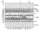
図7に示すように、第1基板SUB1は、絶縁基板10、絶縁層11乃至16、下側遮光層US、半導体層SC、スイッチング素子SW、共通電極CE、画素電極PE、及び配向膜AL1を備えている。絶縁基板10は、有機絶縁材料としてポリイミドなどの樹脂材料によって形成され、可撓性及び光透過性を有する基板である。絶縁基板10は、第1主面1を含んでいる。
FIG. 7 is a sectional view showing a part of the display panel PNL. The illustrated configuration example of the pixel PX corresponds to an example in which a display mode using a horizontal electric field is applied.
As shown in FIG. 7, the first substrate SUB1 includes an insulating
絶縁層11は、絶縁基板10の上に配置されている。下側遮光層USは、絶縁層11の上に位置し、絶縁層12によって覆われている。なお、第1基板SUB1は、絶縁層11無しに形成されてもよく、この場合、下側遮光層USは、絶縁基板10の上に位置している。半導体層SCは、絶縁層12の上に位置し、絶縁層13によって覆われている。半導体層SCは、例えば、多結晶シリコンによって形成されているが、非晶質シリコンや酸化物半導体によって形成されていてもよい。
The insulating
スイッチング素子SWにおいて、ゲート電極GE1及びGE2は、絶縁層13の上に位置し、絶縁層14によって覆われている。ゲート電極GE1及びGE2は、図5に示したいずれかの走査線Gと電気的に接続されている。ソース電極SE及びドレイン電極DEは、絶縁層14の上に位置し、絶縁層15によって覆われている。ソース電極SEは、図5に示したいずれかの信号線Sと電気的に接続されている。ソース電極SEは、絶縁層13及び14を貫通するコンタクトホールCH1を介して半導体層SCにコンタクトしている。ドレイン電極DEは、絶縁層13及び14を貫通するコンタクトホールCH2を介して半導体層SCにコンタクトしている。
In the switching element SW, the gate electrodes GE1 and GE2 are located on the insulating layer 13 and are covered by the insulating layer. The gate electrodes GE1 and GE2 are electrically connected to one of the scanning lines G shown in FIG. The source electrode SE and the drain electrode DE are located on the insulating layer 14 and are covered by the insulating
共通電極CEは、絶縁層15の上に位置し、絶縁層16によって覆われている。画素電極PEは、絶縁層16の上に位置し、配向膜AL1によって覆われている。画素電極PEの一部は、絶縁層16を介して共通電極CEと対向している。共通電極CE及び画素電極PEは、インジウム・ティン・オキサイド(ITO)やインジウム・ジンク・オキサイド(IZO)などの透明な導電材料によって形成されている。画素電極PEは、共通電極CEの開口と重畳する位置において、絶縁層15及び16を貫通するコンタクトホールCH3を介してドレイン電極DEにコンタクトしている。なお、絶縁層11乃至14、及び、絶縁層16は、例えばシリコン酸化物、シリコン窒化物、シリコン酸窒化物などの無機絶縁材料で形成された無機絶縁層であり、単層構造であってもよいし、多層構造であってもよい。絶縁層15は、樹脂として例えばアクリル樹脂などの有機絶縁材料で形成された有機絶縁層である。
The common electrode CE is located on the insulating
第2基板SUB2は、絶縁基板20、絶縁層21、遮光層BM、カラーフィルタ層CF、オーバーコート層OC、及び配向膜AL2を備えている。絶縁基板20は、有機絶縁材料としてポリイミドなどの樹脂材料によって形成され、可撓性及び光透過性を有する基板である。絶縁基板20は、第4主面4を含んでいる。絶縁層21は、例えばシリコン酸化物、シリコン窒化物、シリコン酸窒化物などの無機絶縁層であり、単層構造であってもよいし、多層構造であってもよい。なお、第2基板SUB2は、絶縁層21無しに形成されてもよく、この場合、遮光層BM及びカラーフィルタ層CFは、絶縁基板20の第1基板SUB1と対向する側に位置している。
The second substrate SUB2 includes an insulating
遮光層BM及びカラーフィルタ層CFは、絶縁層21の第1基板SUB1と対向する側に位置している。遮光層BMは、図6などに示した遮光層LSと同一材料を用いて一括して形成可能である。遮光層BMは、信号線Sや走査線Gやスイッチング素子SWなどの配線部とそれぞれ対向する位置に配置されている。カラーフィルタ層CFは、画素電極PEと対向する位置に配置され、その一部が遮光層BMに重なっている。オーバーコート層OCは、カラーフィルタ層CFを覆っている。配向膜AL2は、オーバーコート層OCを覆っている。
The light shielding layer BM and the color filter layer CF are located on the side of the insulating
液晶層LCは、第1基板SUB1と第2基板SUB2との間に位置し、配向膜AL1と配向膜AL2との間に保持されている。液晶層LCは、液晶分子を含んでいる。このような液晶層LCは、ポジ型(誘電率異方性が正)の液晶材料、あるいは、ネガ型(誘電率異方性が負)の液晶材料によって構成されている。
ここで、絶縁基板10の厚みT10及び絶縁基板20の厚みT20は、ぞれぞれ、表示領域DA、額縁領域FA、及び周辺領域APの全体にわたって均一である。
The liquid crystal layer LC is located between the first substrate SUB1 and the second substrate SUB2, and is held between the alignment films AL1 and AL2. The liquid crystal layer LC contains liquid crystal molecules. Such a liquid crystal layer LC is made of a positive liquid crystal material (having a positive dielectric anisotropy) or a negative liquid crystal material (having a negative dielectric anisotropy).
Here, the thickness T10 of the insulating
図8は、図1の線VIII−VIIIに沿った表示装置DSPを示す断面図である。
図8に示すように、第1光学フィルムOF1は、表示セルCLに固定され、表示セルCLと照明装置ILとの間に位置している。第1光学フィルムOF1は、照明装置ILの上面MU、第1側面MS1、第3側面MS3、及び下面MBに接触している。
FIG. 8 is a sectional view showing the display device DSP along the line VIII-VIII in FIG.
As shown in FIG. 8, the first optical film OF1 is fixed to the display cell CL and is located between the display cell CL and the lighting device IL. The first optical film OF1 is in contact with the upper surface MU, the first side surface MS1, the third side surface MS3, and the lower surface MB of the lighting device IL.
表示パネルPNL(表示セルCL)の周辺領域AP1において、第1領域AP1aは、第1角部C1aと対向し、折れ曲がっている。第2領域AP1bは、第1側面MS1と対向している。第3領域AP1cは、第2角部C2aと対向し、折れ曲がっている。第4領域AP1dは、下面MBと対向している。
表示パネルPNL(表示セルCL)の周辺領域AP3において、第1領域AP3aは、第1角部C1cと対向し、折れ曲がっている。第2領域AP3bは、第3側面MS3と対向している。第3領域AP3cは、第2角部C2cと対向し、折れ曲がっている。第4領域AP3dは、下面MBと対向している。
In the peripheral area AP1 of the display panel PNL (display cell CL), the first area AP1a faces the first corner C1a and is bent. The second region AP1b faces the first side surface MS1. The third area AP1c faces the second corner C2a and is bent. The fourth area AP1d faces the lower surface MB.
In the peripheral area AP3 of the display panel PNL (display cell CL), the first area AP3a faces the first corner C1c and is bent. The second region AP3b faces the third side surface MS3. The third area AP3c faces the second corner C2c and is bent. The fourth area AP3d faces the lower surface MB.
図9は、図1の線IX−IXに沿った表示装置DSPを示す断面図である。
図9に示すように、第1光学フィルムOF1は、さらに照明装置ILの第2側面MS2及び第4側面MS4に接触している。
FIG. 9 is a sectional view showing the display device DSP along the line IX-IX in FIG.
As shown in FIG. 9, the first optical film OF1 is further in contact with the second side surface MS2 and the fourth side surface MS4 of the lighting device IL.
表示パネルPNL(表示セルCL)の周辺領域AP2において、第1領域AP2aは、第1角部C1bと対向し、折れ曲がっている。第2領域AP2bは、第2側面MS2と対向している。第3領域AP2cは、第2角部C2bと対向し、折れ曲がっている。第4領域AP2dは、下面MBと対向している。
表示パネルPNL(表示セルCL)の周辺領域AP4において、第1領域AP4aは、第1角部C1dと対向し、折れ曲がっている。第2領域AP4bは、第4側面MS4と対向している。第3領域AP4cは、第2角部C2dと対向し、折れ曲がっている。第4領域AP4dは、下面MBと対向している。
In the peripheral area AP2 of the display panel PNL (display cell CL), the first area AP2a faces the first corner C1b and is bent. The second area AP2b faces the second side surface MS2. The third area AP2c faces the second corner C2b and is bent. The fourth area AP2d faces the lower surface MB.
In the peripheral area AP4 of the display panel PNL (display cell CL), the first area AP4a faces the first corner C1d and is bent. The second region AP4b faces the fourth side surface MS4. The third area AP4c faces the second corner C2d and is bent. The fourth area AP4d faces the lower surface MB.
次に、上記表示セルCLの端部の構造について説明する。ここでは、周辺領域AP1を含む上記表示セルCLの端部の構造について代表して説明する。なお、後述する説明は、他の周辺領域AP2,AP3,AP4の構造にも適用可能である。図10は、上記表示セルCLの一部を展開して示す断面図である。 Next, the structure of the end of the display cell CL will be described. Here, the structure of the end of the display cell CL including the peripheral area AP1 will be described as a representative. Note that the description to be described later is also applicable to the structure of other peripheral areas AP2, AP3, and AP4. FIG. 10 is a sectional view showing a part of the display cell CL in an expanded manner.
図10に示すように、第1主面1から第4主面4までの距離を第1距離D1とする。ここで、第1距離D1は図10における第3方向Zの直線距離である。又は、第1距離D1は第1主面1から第4主面4までの最短距離である。額縁領域FAの第1距離D1は、表示領域DAの第1距離D1と同一である。周辺領域AP1の第1距離D1うち少なくとも第1領域AP1aの第1距離D1は、表示領域DAの第1距離D1より短い。本実施形態において、第2領域AP1b、第3領域AP1c及び第4領域AP1dの第1距離D1は、第1領域AP1aの第1距離D1と同一である。例えば、第2領域AP1bの第1距離D1は、表示領域DAの第1距離D1より短い。
As shown in FIG. 10, a distance from the first
第2主面2から第3主面3までの距離を第2距離D2とする。ここで、第2距離D2は図10における第3方向Zの直線距離である。又は、第2距離D2は第2主面2から第3主面3までの最短距離である。額縁領域FAの第2距離D2は、表示領域DAの第2距離D2と、同一である。周辺領域AP1の第2距離D2のうち少なくとも第1領域AP1aの第2距離D2は、表示領域DAの第2距離D2より短い。本実施形態において、第2領域AP1b、第3領域AP1c及び第4領域AP1dの第2距離D2は、第1領域AP1aの第2距離D2と同一である。
The distance from the second
上述した第1距離D1及び第2距離D2の関係を得るため、本実施形態ではスペーサSPにて調整している。表示セルCLは、複数のスペーサSPを有している。スペーサSPは、第1基板SUB1と第2基板SUB2との間に位置し、第1基板SUB1と第2基板SUB2との間の隙間を保持している。複数のスペーサSPは、表示領域DA及び額縁領域FAに位置した複数の第1スペーサSP1と、周辺領域AP1のうち少なくとも第1領域AP1aに位置した複数の第2スペーサSP2と、を有している。本実施形態において、第2領域AP1b、第3領域AP1c及び第4領域AP1dのスペーサSPも第2スペーサSP2である。第2主面2と第3主面3とが対向する方向において、第2スペーサSP2の長さL2は、第1スペーサSP1の長L1さより短い。
In order to obtain the above-described relationship between the first distance D1 and the second distance D2, in the present embodiment, the adjustment is performed using the spacer SP. The display cell CL has a plurality of spacers SP. The spacer SP is located between the first substrate SUB1 and the second substrate SUB2, and holds a gap between the first substrate SUB1 and the second substrate SUB2. The plurality of spacers SP include a plurality of first spacers SP1 located in the display area DA and the frame area FA, and a plurality of second spacers SP2 located in at least the first area AP1a of the peripheral area AP1. . In the present embodiment, the spacers SP in the second region AP1b, the third region AP1c, and the fourth region AP1d are also the second spacers SP2. In the direction in which the second
複数の第1スペーサSP1及び複数の第2スペーサSP2は、それぞれ、第1基板SUB1及び第2基板SUB2の何れか一方の基板に固定され他方の基板の主面である第2主面2又は第3主面3に接触する柱状スペーサである。本実施形態において、第1スペーサSP1及び第2スペーサSP2は、それぞれ、第2基板SUB2に固定され第1基板SUB1の第2主面2に接触している。そのため、第2スペーサSP2の高さ(L2)は、第1スペーサSP1の高さ(L1)未満である。
The plurality of first spacers SP1 and the plurality of second spacers SP2 are fixed to one of the first substrate SUB1 and the second substrate SUB2, respectively, and the second
額縁領域FAと第1領域AP1aの境界近傍において、第1基板SUB1及び第2基板SUB2の両方に歪みが生じている。但し、本実施形態と異なり、上記境界近傍において、第1基板SUB1及び第2基板SUB2の一方のみに歪みが生じていてもよい。 Near the boundary between the frame area FA and the first area AP1a, both the first substrate SUB1 and the second substrate SUB2 are distorted. However, unlike this embodiment, in the vicinity of the boundary, only one of the first substrate SUB1 and the second substrate SUB2 may be distorted.
上記のように構成された一実施形態に係る表示装置DSPよれば、表示パネルPNLの周辺領域AP1,AP2,AP3,AP4を照明装置ILに沿って折り曲げることができる。図2に示したように、表示装置DSPの裏面(下面MB)側に、周辺領域AP1,AP2,AP3,AP4を折りこむことができる。これにより、表示装置DSPの表面の額縁を縮小することができる。 According to the display device DSP according to the embodiment configured as described above, the peripheral regions AP1, AP2, AP3, and AP4 of the display panel PNL can be bent along the illumination device IL. As shown in FIG. 2, the peripheral regions AP1, AP2, AP3, and AP4 can be folded on the back surface (lower surface MB) of the display device DSP. Thereby, the frame on the surface of the display device DSP can be reduced.
周辺領域AP1に注目すると、第1領域AP1a及び第3領域AP1cのそれぞれの第1距離D1は、表示領域DAの第1距離D1より短い。第1領域AP1a及び第3領域AP1cのそれぞれの第1距離D1が表示領域DAの第1距離D1と同一である場合と比較して、表示パネルPNLを折り曲げた際に表示セルCLに加わる応力(ストレス)を低減することができる。これにより、第1領域AP1a及び第3領域AP1cなどの周辺領域AP1において、絶縁基板10,20の破損、座屈の発生、歪みの発生などを低減することができる。ひいては、周辺領域AP1に位置する配線の断線など、不具合の発生を低減することができる。なお、上記歪みとは、額縁領域FAと第1領域AP1aの境界近傍に生じる所望の歪みではなく、不所望の歪みを言う。
上記のことから、信頼性の高い表示装置DSPを得ることができる。
Focusing on the peripheral area AP1, the first distance D1 of each of the first area AP1a and the third area AP1c is shorter than the first distance D1 of the display area DA. The stress applied to the display cell CL when the display panel PNL is bent, as compared with the case where the first distance D1 of each of the first area AP1a and the third area AP1c is the same as the first distance D1 of the display area DA ( Stress) can be reduced. Accordingly, in the peripheral regions AP1 such as the first region AP1a and the third region AP1c, it is possible to reduce damage, buckling, distortion, and the like of the insulating
From the above, a highly reliable display device DSP can be obtained.
(変形例1)
次に、上記実施形態の変形例1に係る表示装置DSPについて説明する。図11は、上記実施形態の変形例1に係る表示セルCLの一部を展開して示す断面図である。ここでは、表示セルCLの周辺領域AP1の構成を代表して説明する。但し、本変形例1の技術は、上記周辺領域AP2,AP3,AP4にも適用可能である。
(Modification 1)
Next, a display device DSP according to a first modification of the embodiment will be described. FIG. 11 is a cross-sectional view showing a part of a display cell CL according to Modification Example 1 of the embodiment in an expanded manner. Here, the configuration of the peripheral area AP1 of the display cell CL will be described as a representative. However, the technique of the first modification is also applicable to the peripheral areas AP2, AP3, and AP4.
図11に示すように、第2領域AP1bの第1距離D1及び第4領域AP1dの第1距離D1は、それぞれ、表示領域DAの第1距離D1と同一であってもよい。なお、周辺領域AP1の第1距離D1うち第1領域AP1aの第1距離D1は、表示領域DAの第1距離D1より短い。第1領域AP1aの第1距離D1は、第3領域AP1cの第1距離D1と同一である。第1領域AP1aの第2距離D2は、表示領域DAの第2距離D2より短く、第3領域AP1cの第2距離D2と同一である。 As shown in FIG. 11, the first distance D1 of the second area AP1b and the first distance D1 of the fourth area AP1d may be the same as the first distance D1 of the display area DA. The first distance D1 of the first area AP1a among the first distances D1 of the peripheral area AP1 is shorter than the first distance D1 of the display area DA. The first distance D1 of the first area AP1a is the same as the first distance D1 of the third area AP1c. The second distance D2 of the first area AP1a is shorter than the second distance D2 of the display area DA, and is equal to the second distance D2 of the third area AP1c.
上述した第1距離D1及び第2距離D2の関係を得るため、本変形例1ではスペーサSPにて調整している。周辺領域AP1のうち、第2領域AP1b及び第4領域AP1dには第1スペーサSP1が位置し、第1領域AP1a及び第3領域AP1cには第2スペーサSP2が位置している。
上記のように構成された変形例1においても、上記実施形態と同様の効果を得ることができる。
In order to obtain the above-described relationship between the first distance D1 and the second distance D2, in the first modification, the adjustment is performed using the spacer SP. In the peripheral area AP1, the first spacer SP1 is located in the second area AP1b and the fourth area AP1d, and the second spacer SP2 is located in the first area AP1a and the third area AP1c.
In the first modification configured as described above, the same effect as in the above embodiment can be obtained.
(変形例2)
次に、上記実施形態の変形例2に係る表示装置DSPについて説明する。図12は、上記実施形態の変形例2に係る表示セルCLの一部を展開して示す断面図である。ここでは、表示セルCLの周辺領域AP1の構成を代表して説明する。但し、本変形例2の技術は、上記周辺領域AP2,AP3,AP4にも適用可能である。
(Modification 2)
Next, a display device DSP according to a modified example 2 of the embodiment will be described. FIG. 12 is a cross-sectional view showing a part of a display cell CL according to
図12に示すように、複数の第2スペーサSP2は、球状スペーサであってもよい。第2スペーサSP2は、それぞれ第2主面2及び第3主面3に接触している。第2スペーサSP2の直径(L2)は、第1スペーサSP1の高さ(L1)未満である。
上記のように構成された変形例2においても、上記実施形態と同様の効果を得ることができる。
As shown in FIG. 12, the plurality of second spacers SP2 may be spherical spacers. The second spacer SP2 is in contact with the second
In the modified example 2 configured as described above, the same effect as in the above embodiment can be obtained.
(変形例3)
次に、上記実施形態の変形例3に係る表示装置DSPについて説明する。図13は、上記実施形態の変形例3に係る表示セルCLの一部を展開して示す断面図である。ここでは、表示セルCLの周辺領域AP1の構成を代表して説明する。但し、本変形例3の技術は、上記周辺領域AP2,AP3,AP4にも適用可能である。
(Modification 3)
Next, a display device DSP according to a third modification of the embodiment will be described. FIG. 13 is a cross-sectional view showing a part of a display cell CL according to a third modification of the embodiment in an expanded manner. Here, the configuration of the peripheral area AP1 of the display cell CL will be described as a representative. However, the technique of the third modification is applicable to the above-described peripheral areas AP2, AP3, and AP4.
図13に示すように、第1基板SUB1は、絶縁基板10と、有機絶縁層としての絶縁層15と、を備えている。ここでは、第1基板SUB1のうち絶縁基板10及び絶縁層15以外の図示を割愛している。なお、図5から分かるように、表示セルCLの周辺領域AP1には、配線、パッド、及び回路が設けられている。そのため、第1基板SUB1のうち図13に示す部分は、他の絶縁層、及び導電層を含んでいる。
As shown in FIG. 13, the first substrate SUB1 includes an insulating
絶縁層15は、絶縁基板10より第2基板SUB2側に位置している。周辺領域AP1のうち少なくとも第1領域AP1a及び第3領域AP1cにおいて、絶縁層15は、複数の凹部15aを含んでいる。複数の凹部15aは、それぞれ第2基板SUB2から絶縁基板10に向かって凹んでいる。凹部15aは、絶縁層15を貫通している。なお、凹部15aは、凹んでいればよく、絶縁層15を貫通していなくともよい。図13に示す例では、第2主面2は、絶縁層15のうち第2基板SUB2側の面である。凹部15aにおいて、第2主面2は、絶縁基板10のうち第2基板SUB2側の面である。
但し、第2主面2は、図13に示す例に限定されるものではない。第1基板SUB1のうち絶縁層15より第2基板SUB2側の層が、第2主面2を有していてもよい。同様に、凹部15aにおいても、絶縁基板10より第2基板SUB2側の層が、第2主面2を有していてもよい。
The insulating
However, the second
複数のスペーサSPは、柱状スペーサであり、表示領域DA及び額縁領域FAに位置した複数の第1スペーサSP1と、周辺領域AP1のうち少なくとも第1領域AP1a及び第3領域AP1cに位置した複数の第2スペーサSP2と、を有している。各々の第2スペーサSP2の高さ(L2)は、各々の第1スペーサSP1の高さ(L1)と同一である。
本実施形態において、凹部15a及び第2スペーサSP2は、第1領域AP1a及び第3領域AP1cだけではなく、第2領域AP1b、及び第4領域AP1dにも設けられている。
The plurality of spacers SP are columnar spacers, and the plurality of first spacers SP1 located in the display area DA and the frame area FA, and the plurality of first spacers located in at least the first area AP1a and the third area AP1c of the peripheral area AP1. And two spacers SP2. The height (L2) of each second spacer SP2 is the same as the height (L1) of each first spacer SP1.
In the present embodiment, the
第1スペーサSP1及び第2スペーサSP2は、第2基板SUB2に固定され、第2主面2に接触している。第1スペーサSP1は、第2主面2として絶縁層15のうち第2基板SUB2側の面に接触している。全てのスペーサSPは、第2基板SUB2に共に固定されている方が望ましい。但し、第1スペーサSP1に関しては、第1基板SUB1に固定され、第3主面3に接触していてもよい。複数の第2スペーサSP2は、それぞれ対応する凹部15aに入り、第2主面2に接触している。
The first spacer SP1 and the second spacer SP2 are fixed to the second substrate SUB2 and are in contact with the second
上記のことから、絶縁層15の厚みの分、周辺領域AP1の第1距離D1は、表示領域DAの第1距離D1より短い。なお、周辺領域AP1の第2距離D2も、絶縁層15の厚みの分、表示領域DAの第2距離D2より短い。
上記のように構成された変形例3においても、上記実施形態と同様の効果を得ることができる。
From the above, the first distance D1 of the peripheral area AP1 is shorter than the first distance D1 of the display area DA by the thickness of the insulating
In the third modification configured as described above, the same effect as in the above embodiment can be obtained.
(変形例4)
次に、上記実施形態の変形例4に係る表示装置DSPについて説明する。図14は、上記実施形態の変形例4に係る表示セルCLの一部を展開して示す断面図である。ここでは、表示セルCLの周辺領域AP1の構成を代表して説明する。但し、本変形例4の技術は、上記周辺領域AP2,AP3,AP4にも適用可能である。
(Modification 4)
Next, a display device DSP according to a modified example 4 of the embodiment will be described. FIG. 14 is a cross-sectional view showing a part of a display cell CL according to
図14に示すように、複数のスペーサSPは、表示領域DA及び額縁領域FAに位置した複数の第1スペーサSP1と、周辺領域AP1のうち少なくとも第1領域AP1a及び第3領域AP1cに位置した複数の第2スペーサSP2と、を有している。第2主面2と第3主面3とが対向する方向において、各々の第2スペーサSP2の長さL2は、各々の第1スペーサSP1の長さL1と同一である。額縁領域FAの第2距離D2及び周辺領域AP1のうち少なくとも第1領域AP1a及び第3領域AP1cの第2距離D2は、それぞれ、表示領域DAの第2距離D2と、同一である。
As shown in FIG. 14, the plurality of spacers SP include a plurality of first spacers SP1 located in the display area DA and the frame area FA, and a plurality of spacers SP located in at least the first area AP1a and the third area AP1c of the peripheral area AP1. And the second spacer SP2. In the direction in which the second
絶縁層15は、表示領域DA及び額縁領域FAに位置し、周辺領域AP1のうち少なくとも第1領域AP1a及び第3領域AP1cに位置していない。
本実施形態において、絶縁層15は、第2領域AP1b、及び第4領域AP1dにも位置していない。第2スペーサSP2は、第2領域AP1b、及び第4領域AP1dにも設けられている。表示領域DA及び額縁領域FAにおいて、第1スペーサSP1は絶縁層15と対向している。
The insulating
In the present embodiment, the insulating
上記のことから、絶縁層15の厚みの分、周辺領域AP1の第1距離D1は、表示領域DAの第1距離D1より短い。但し、周辺領域AP1の第2距離D2は、表示領域DAの第2距離D2と同一である。
上記のように構成された変形例4においても、上記実施形態と同様の効果を得ることができる。
From the above, the first distance D1 of the peripheral area AP1 is shorter than the first distance D1 of the display area DA by the thickness of the insulating
In the modified example 4 configured as described above, the same effect as the above embodiment can be obtained.
本発明の一実施形態及び変形例を説明したが、上記の実施形態及び変形例は、例として提示したものであり、発明の範囲を限定することは意図していない。上記の新規な実施形態及び変形例は、その他の様々な形態で実施されることが可能であり、発明の要旨を逸脱しない範囲で、種々の省略、置き換え、変更を行うことができる。上記の実施形態やその変形例は、発明の範囲や要旨に含まれるとともに、特許請求の範囲に記載された発明とその均等の範囲に含まれる。必要に応じて、上記の実施形態及び変形例を組合せることも可能である。 Although the embodiment and the modified example of the present invention have been described, the above-described embodiment and the modified example are presented as examples, and are not intended to limit the scope of the invention. The above-described novel embodiments and modified examples can be implemented in other various forms, and various omissions, replacements, and changes can be made without departing from the spirit of the invention. The above embodiment and its modified examples are included in the scope and the gist of the invention, and are also included in the invention described in the claims and its equivalents. It is also possible to combine the above-described embodiments and modified examples as needed.
例えば、図15に示すように、上記変形例1(図11)と上記変形例3(図13)とを組み合わせてもよい。上記のことから、絶縁層15の厚みの分、第2領域AP1b及び第4領域AP1dの第1距離D1は、表示領域DAの第1距離D1より短い。そして、第2スペーサSP2の高さ(L2)と第1スペーサSP1の高さ(L1)との差分だけ、第1領域AP1a及び第3領域AP1cの第1距離D1は、第2領域AP1b及び第4領域AP1dの第1距離D1より短い。
For example, as shown in FIG. 15, the above-described first modification (FIG. 11) and the third modification (FIG. 13) may be combined. From the above, the first distance D1 of the second region AP1b and the fourth region AP1d is shorter than the first distance D1 of the display region DA by the thickness of the insulating
DSP…表示装置、IL…照明装置、MS1,MS2,MS3,MS4…側面、
C1a,C1b,C1c,C1d,C2a,C2b,C2c,C2d…角部、
MU…上面、MB…下面、PNL…表示パネル、DA…表示領域、NDA…非表示領域、
FA…額縁領域、AP1,AP2,AP3,AP4…周辺領域、
AP1a,AP2a,AP3a,AP4a…第1領域、
AP1b,AP2b,AP3b,AP4b…第2領域、
AP1c,AP2c,AP3c,AP4c…第3領域、
AP1d,AP2d,AP3d,AP4d…第4領域、
CL…表示セル、LC…液晶層、SUB1,SUB2…基板、10,20…絶縁基板、
15…絶縁層、15a…凹部、SL…シール材、SP,SP1,SP2…スペーサ、
1,2,3,4…主面、D1,D2…距離、L1,L2…長さ。
DSP: display device, IL: lighting device, MS1, MS2, MS3, MS4: side surface,
C1a, C1b, C1c, C1d, C2a, C2b, C2c, C2d...
MU: upper surface, MB: lower surface, PNL: display panel, DA: display area, NDA: non-display area,
FA: frame area, AP1, AP2, AP3, AP4: peripheral area,
AP1a, AP2a, AP3a, AP4a ... first area,
AP1b, AP2b, AP3b, AP4b ... second area,
AP1c, AP2c, AP3c, AP4c ... third area,
AP1d, AP2d, AP3d, AP4d ... the fourth area,
CL: display cell, LC: liquid crystal layer, SUB1, SUB2: substrate, 10, 20: insulating substrate,
15 insulating layer, 15a recess, SL sealing material, SP, SP1, SP2 spacer
1, 2, 3, 4... Main surface, D1, D2... Distance, L1, L2.
Claims (12)
前記第2主面に隙間を置いて対向した第3主面及び前記第3主面とは反対側の第4主面とを含み、前記表示領域及び前記非表示領域に位置した第2基板と、
前記非表示領域に位置し、前記第1基板と前記第2基板とを接合したシール材と、
前記第1基板、前記第2基板、及び前記シール材で囲まれた空間に設けられた液晶層と、を有する表示セルを備え、
前記非表示領域は、第1領域を含む周辺領域と、前記表示領域及び前記周辺領域の間に位置し前記表示領域を囲む額縁領域と、を有し、
前記シール材と前記液晶層との境界は、前記額縁領域に位置し、
前記第1主面から前記第4主面までの距離を第1距離とすると、
前記額縁領域の前記第1距離は、前記表示領域の前記第1距離と、同一であり、
前記周辺領域の前記第1距離うち少なくとも前記第1領域の前記第1距離は、前記表示領域の前記第1距離より短い、
表示装置。 A first substrate including a first main surface and a second main surface opposite to the first main surface, the first substrate being located in a display region and a non-display region outside the display region;
A second substrate positioned in the display area and the non-display area, including a third main surface facing the second main surface with a gap therebetween, and a fourth main surface opposite to the third main surface; ,
A sealing material that is located in the non-display area and that joins the first substrate and the second substrate;
A display cell having a liquid crystal layer provided in a space surrounded by the first substrate, the second substrate, and the sealant;
The non-display area has a peripheral area including a first area, and a frame area located between the display area and the peripheral area and surrounding the display area,
A boundary between the sealing material and the liquid crystal layer is located in the frame region,
When the distance from the first main surface to the fourth main surface is a first distance,
The first distance of the frame area is the same as the first distance of the display area;
At least the first distance of the first region among the first distances of the peripheral region is shorter than the first distance of the display region;
Display device.
前記第2基板は、前記第4主面を含み有機絶縁材料で形成された第2絶縁基板を有し、
前記第1絶縁基板及び前記第2絶縁基板は、ぞれぞれ、前記表示領域、前記額縁領域、及び前記周辺領域の全体にわたって均一の厚みを有する、
請求項1に記載の表示装置。 The first substrate has a first insulating substrate including the first main surface and formed of an organic insulating material,
The second substrate includes a second insulating substrate including the fourth main surface and formed of an organic insulating material,
The first insulating substrate and the second insulating substrate each have a uniform thickness over the entire display region, the frame region, and the peripheral region,
The display device according to claim 1.
前記額縁領域の前記第2距離は、前記表示領域の前記第2距離と、同一であり、
前記周辺領域の前記第2距離のうち少なくとも前記第1領域の前記第2距離は、前記表示領域の前記第2距離より短い、
請求項1に記載の表示装置。 Assuming that the distance from the second main surface to the third main surface is a second distance,
The second distance of the frame area is the same as the second distance of the display area;
At least the second distance of the first region among the second distances of the peripheral region is shorter than the second distance of the display region;
The display device according to claim 1.
前記複数のスペーサは、前記表示領域及び前記額縁領域に位置した複数の第1スペーサと、前記周辺領域のうち少なくとも前記第1領域に位置した複数の第2スペーサと、を有し、
前記第2主面と前記第3主面とが対向する方向において、
各々の前記第2スペーサの長さは、各々の前記第1スペーサの長さより短い、
請求項3に記載の表示装置。 The display cell further includes a plurality of spacers located between the first substrate and the second substrate, and holding a gap between the first substrate and the second substrate,
The plurality of spacers include a plurality of first spacers located in the display area and the frame area, and a plurality of second spacers located in at least the first area of the peripheral area,
In a direction in which the second main surface and the third main surface face each other,
A length of each of the second spacers is shorter than a length of each of the first spacers;
The display device according to claim 3.
各々の前記第2スペーサの高さは、各々の前記第1スペーサの高さ未満である、
請求項4に記載の表示装置。 The plurality of first spacers and the plurality of second spacers are respectively fixed to one of the first substrate and the second substrate, and the second main surface or the main surface of the other substrate is a main surface of the other substrate. A columnar spacer that contacts the third main surface,
A height of each of the second spacers is less than a height of each of the first spacers;
The display device according to claim 4.
前記複数の第2スペーサは、それぞれ前記第2主面及び前記第3主面に接触する球状スペーサであり、
各々の前記第2スペーサの直径は、各々の前記第1スペーサの高さ未満である、
請求項4に記載の表示装置。 The plurality of first spacers are each fixed to one of the first substrate and the second substrate, and are columnar in contact with the second main surface or the third main surface that is a main surface of the other substrate. Spacer
The plurality of second spacers are spherical spacers that are in contact with the second main surface and the third main surface, respectively.
A diameter of each of the second spacers is less than a height of each of the first spacers;
The display device according to claim 4.
前記第1基板は、前記第1主面を含み有機絶縁材料で形成された第1絶縁基板と、前記第1絶縁基板より前記第2基板側に位置した有機絶縁層と、を有し、
前記第2基板は、前記第4主面を含み有機絶縁材料で形成された第2絶縁基板を有し、
前記周辺領域のうち少なくとも前記第1領域において、前記有機絶縁層は、それぞれ前記第2基板から前記第1絶縁基板に向かって凹んだ複数の凹部を含み、
前記複数のスペーサは、前記表示領域及び前記額縁領域に位置した複数の第1スペーサと、前記周辺領域のうち少なくとも前記第1領域に位置した複数の第2スペーサと、を有し、
各々の前記第2スペーサの高さは、各々の前記第1スペーサの高さと同一であり、
前記複数の第1スペーサは、それぞれ、前記第1基板及び前記第2基板の何れか一方の基板に固定され他方の基板の主面である前記第2主面又は前記第3主面に接触する柱状スペーサであり、
前記複数の第2スペーサは、それぞれ、前記第2基板に固定され対応する前記凹部に入り前記第2主面に接触する柱状スペーサである、
請求項3に記載の表示装置。 The display cell further includes a plurality of spacers located between the first substrate and the second substrate, and holding a gap between the first substrate and the second substrate,
The first substrate includes a first insulating substrate including the first main surface and formed of an organic insulating material, and an organic insulating layer positioned closer to the second substrate than the first insulating substrate,
The second substrate includes a second insulating substrate including the fourth main surface and formed of an organic insulating material,
In at least the first region of the peripheral region, the organic insulating layer includes a plurality of recesses each recessed from the second substrate toward the first insulating substrate,
The plurality of spacers include a plurality of first spacers located in the display area and the frame area, and a plurality of second spacers located in at least the first area of the peripheral area,
A height of each of the second spacers is equal to a height of each of the first spacers;
The plurality of first spacers are fixed to one of the first substrate and the second substrate, respectively, and are in contact with the second main surface or the third main surface, which is the main surface of the other substrate. A columnar spacer,
Each of the plurality of second spacers is a columnar spacer that is fixed to the second substrate and enters the corresponding recess and contacts the second main surface.
The display device according to claim 3.
前記複数のスペーサは、前記表示領域及び前記額縁領域に位置した複数の第1スペーサと、前記周辺領域のうち少なくとも前記第1領域に位置した複数の第2スペーサと、を有し、
前記第2主面と前記第3主面とが対向する方向において、
各々の前記第2スペーサの長さは、各々の前記第1スペーサの長さと同一であり、
前記第2主面から前記第3主面までの距離を第2距離とすると、
前記額縁領域の前記第2距離及び前記周辺領域のうち少なくとも前記第1領域の前記第2距離は、それぞれ、前記表示領域の前記第2距離と、同一であり、
前記第1基板は、前記第1主面を含み有機絶縁材料で形成された第1絶縁基板と、前記第1絶縁基板より前記第2基板側に位置した有機絶縁層と、を有し、
前記第2基板は、前記第4主面を含み有機絶縁材料で形成された第2絶縁基板を有し、
前記有機絶縁層は、前記表示領域及び前記額縁領域に位置し、前記周辺領域のうち少なくとも前記第1領域に位置していない、
請求項1に記載の表示装置。 The display cell further includes a plurality of spacers located between the first substrate and the second substrate, and holding a gap between the first substrate and the second substrate,
The plurality of spacers include a plurality of first spacers located in the display area and the frame area, and a plurality of second spacers located in at least the first area of the peripheral area,
In a direction in which the second main surface and the third main surface face each other,
A length of each of the second spacers is the same as a length of each of the first spacers;
Assuming that the distance from the second main surface to the third main surface is a second distance,
At least the second distance of the first region among the second distance of the frame region and the peripheral region is the same as the second distance of the display region, respectively.
The first substrate includes a first insulating substrate including the first main surface and formed of an organic insulating material, and an organic insulating layer positioned closer to the second substrate than the first insulating substrate,
The second substrate includes a second insulating substrate including the fourth main surface and formed of an organic insulating material,
The organic insulating layer is located in the display area and the frame area, and is not located in at least the first area of the peripheral area;
The display device according to claim 1.
前記表示セルにおいて、
前記表示領域及び前記額縁領域は、前記上面と対向し、
前記周辺領域は、前記第1側面と対向する第2領域をさらに含み、
前記第1領域は、前記額縁領域と前記第2領域との間に位置し、前記第1角部と対向し、折れ曲がっている、
請求項1に記載の表示装置。 Further comprising a plate-shaped lighting device having an upper surface, a first side surface, and a first corner located between the upper surface and the first side surface,
In the display cell,
The display area and the frame area face the upper surface,
The peripheral region further includes a second region facing the first side surface,
The first region is located between the frame region and the second region, faces the first corner, and is bent.
The display device according to claim 1.
請求項9に記載の表示装置。 The first distance of the second area is shorter than the first distance of the display area;
The display device according to claim 9.
請求項9に記載の表示装置。 The first distance of the first area is the same as the first distance of the display area,
The display device according to claim 9.
前記表示セルにおいて、
前記周辺領域は、第3領域と、前記下面と対向する第4領域と、をさらに含み、
前記第3領域は、前記第2領域と前記第4領域との間に位置し、前記第2角部と対向し、折れ曲がっている、
請求項9に記載の表示装置。 The lighting device further includes a lower surface opposite to the upper surface, and a second corner located between the lower surface and the first side surface,
In the display cell,
The peripheral region further includes a third region and a fourth region facing the lower surface,
The third region is located between the second region and the fourth region, faces the second corner, and is bent;
The display device according to claim 9.
Priority Applications (2)
| Application Number | Priority Date | Filing Date | Title |
|---|---|---|---|
| JP2018121866A JP2020003601A (en) | 2018-06-27 | 2018-06-27 | Display |
| PCT/JP2019/022997 WO2020003998A1 (en) | 2018-06-27 | 2019-06-10 | Display device |
Applications Claiming Priority (1)
| Application Number | Priority Date | Filing Date | Title |
|---|---|---|---|
| JP2018121866A JP2020003601A (en) | 2018-06-27 | 2018-06-27 | Display |
Publications (1)
| Publication Number | Publication Date |
|---|---|
| JP2020003601A true JP2020003601A (en) | 2020-01-09 |
Family
ID=68984826
Family Applications (1)
| Application Number | Title | Priority Date | Filing Date |
|---|---|---|---|
| JP2018121866A Pending JP2020003601A (en) | 2018-06-27 | 2018-06-27 | Display |
Country Status (2)
| Country | Link |
|---|---|
| JP (1) | JP2020003601A (en) |
| WO (1) | WO2020003998A1 (en) |
Families Citing this family (1)
| Publication number | Priority date | Publication date | Assignee | Title |
|---|---|---|---|---|
| JP2021114587A (en) * | 2020-01-21 | 2021-08-05 | 株式会社ジャパンディスプレイ | Flexible substrate |
Family Cites Families (4)
| Publication number | Priority date | Publication date | Assignee | Title |
|---|---|---|---|---|
| JP3297385B2 (en) * | 1998-10-21 | 2002-07-02 | 株式会社東芝 | Liquid crystal display |
| JP2004151549A (en) * | 2002-10-31 | 2004-05-27 | Seiko Epson Corp | Electro-optical panel, electro-optical device, electronic equipment, and method for manufacturing electro-optical panel |
| CN105659310B (en) * | 2013-08-13 | 2021-02-26 | 飞利斯有限公司 | Optimization of electronic display area |
| KR102242439B1 (en) * | 2014-09-30 | 2021-04-20 | 삼성디스플레이 주식회사 | Curved liquid crystal display |
-
2018
- 2018-06-27 JP JP2018121866A patent/JP2020003601A/en active Pending
-
2019
- 2019-06-10 WO PCT/JP2019/022997 patent/WO2020003998A1/en active Application Filing
Also Published As
| Publication number | Publication date |
|---|---|
| WO2020003998A1 (en) | 2020-01-02 |
Similar Documents
| Publication | Publication Date | Title |
|---|---|---|
| US11740510B2 (en) | Display device | |
| JP5448940B2 (en) | Liquid crystal display | |
| JP2018049193A (en) | Display device | |
| JP2020027190A (en) | Display device | |
| JP2018112692A (en) | Display | |
| JP2017167527A (en) | Display device | |
| JP2019028139A (en) | Display device | |
| JP2014032346A (en) | Liquid crystal display panel | |
| JP2023174931A (en) | display device | |
| US11809049B2 (en) | Display device | |
| WO2020003998A1 (en) | Display device | |
| WO2019111594A1 (en) | Display apparatus | |
| US11703735B2 (en) | Display device | |
| WO2020080086A1 (en) | Display device | |
| WO2020079963A1 (en) | Display device | |
| WO2020071009A1 (en) | Display device | |
| JP7467688B2 (en) | Display device | |
| JP2020177731A (en) | Cover glass and display device | |
| JP2019215414A (en) | Display device | |
| CN111679519B (en) | Display device | |
| JP7456013B2 (en) | Display device | |
| US11614668B2 (en) | Display device | |
| JP7326558B2 (en) | Display device | |
| US20230359096A1 (en) | Display device | |
| WO2020036041A1 (en) | Display device |