JP2019534148A - PT-NI-IR catalyst for fuel cell - Google Patents
PT-NI-IR catalyst for fuel cell Download PDFInfo
- Publication number
- JP2019534148A JP2019534148A JP2019522524A JP2019522524A JP2019534148A JP 2019534148 A JP2019534148 A JP 2019534148A JP 2019522524 A JP2019522524 A JP 2019522524A JP 2019522524 A JP2019522524 A JP 2019522524A JP 2019534148 A JP2019534148 A JP 2019534148A
- Authority
- JP
- Japan
- Prior art keywords
- catalyst
- layer
- nickel
- range
- platinum
- Prior art date
- Legal status (The legal status is an assumption and is not a legal conclusion. Google has not performed a legal analysis and makes no representation as to the accuracy of the status listed.)
- Pending
Links
Images


Classifications
-
- H—ELECTRICITY
- H01—ELECTRIC ELEMENTS
- H01M—PROCESSES OR MEANS, e.g. BATTERIES, FOR THE DIRECT CONVERSION OF CHEMICAL ENERGY INTO ELECTRICAL ENERGY
- H01M4/00—Electrodes
- H01M4/86—Inert electrodes with catalytic activity, e.g. for fuel cells
- H01M4/90—Selection of catalytic material
- H01M4/92—Metals of platinum group
- H01M4/921—Alloys or mixtures with metallic elements
-
- H—ELECTRICITY
- H01—ELECTRIC ELEMENTS
- H01M—PROCESSES OR MEANS, e.g. BATTERIES, FOR THE DIRECT CONVERSION OF CHEMICAL ENERGY INTO ELECTRICAL ENERGY
- H01M4/00—Electrodes
- H01M4/86—Inert electrodes with catalytic activity, e.g. for fuel cells
- H01M4/8647—Inert electrodes with catalytic activity, e.g. for fuel cells consisting of more than one material, e.g. consisting of composites
- H01M4/8657—Inert electrodes with catalytic activity, e.g. for fuel cells consisting of more than one material, e.g. consisting of composites layered
-
- H—ELECTRICITY
- H01—ELECTRIC ELEMENTS
- H01M—PROCESSES OR MEANS, e.g. BATTERIES, FOR THE DIRECT CONVERSION OF CHEMICAL ENERGY INTO ELECTRICAL ENERGY
- H01M4/00—Electrodes
- H01M4/86—Inert electrodes with catalytic activity, e.g. for fuel cells
- H01M4/88—Processes of manufacture
- H01M4/8878—Treatment steps after deposition of the catalytic active composition or after shaping of the electrode being free-standing body
-
- H—ELECTRICITY
- H01—ELECTRIC ELEMENTS
- H01M—PROCESSES OR MEANS, e.g. BATTERIES, FOR THE DIRECT CONVERSION OF CHEMICAL ENERGY INTO ELECTRICAL ENERGY
- H01M4/00—Electrodes
- H01M4/86—Inert electrodes with catalytic activity, e.g. for fuel cells
- H01M4/90—Selection of catalytic material
- H01M4/92—Metals of platinum group
- H01M4/925—Metals of platinum group supported on carriers, e.g. powder carriers
-
- H—ELECTRICITY
- H01—ELECTRIC ELEMENTS
- H01M—PROCESSES OR MEANS, e.g. BATTERIES, FOR THE DIRECT CONVERSION OF CHEMICAL ENERGY INTO ELECTRICAL ENERGY
- H01M4/00—Electrodes
- H01M4/86—Inert electrodes with catalytic activity, e.g. for fuel cells
- H01M4/98—Raney-type electrodes
-
- H—ELECTRICITY
- H01—ELECTRIC ELEMENTS
- H01M—PROCESSES OR MEANS, e.g. BATTERIES, FOR THE DIRECT CONVERSION OF CHEMICAL ENERGY INTO ELECTRICAL ENERGY
- H01M8/00—Fuel cells; Manufacture thereof
- H01M8/10—Fuel cells with solid electrolytes
- H01M2008/1095—Fuel cells with polymeric electrolytes
-
- H—ELECTRICITY
- H01—ELECTRIC ELEMENTS
- H01M—PROCESSES OR MEANS, e.g. BATTERIES, FOR THE DIRECT CONVERSION OF CHEMICAL ENERGY INTO ELECTRICAL ENERGY
- H01M4/00—Electrodes
- H01M4/86—Inert electrodes with catalytic activity, e.g. for fuel cells
- H01M4/88—Processes of manufacture
- H01M4/8825—Methods for deposition of the catalytic active composition
- H01M4/8867—Vapour deposition
- H01M4/8871—Sputtering
-
- Y—GENERAL TAGGING OF NEW TECHNOLOGICAL DEVELOPMENTS; GENERAL TAGGING OF CROSS-SECTIONAL TECHNOLOGIES SPANNING OVER SEVERAL SECTIONS OF THE IPC; TECHNICAL SUBJECTS COVERED BY FORMER USPC CROSS-REFERENCE ART COLLECTIONS [XRACs] AND DIGESTS
- Y02—TECHNOLOGIES OR APPLICATIONS FOR MITIGATION OR ADAPTATION AGAINST CLIMATE CHANGE
- Y02E—REDUCTION OF GREENHOUSE GAS [GHG] EMISSIONS, RELATED TO ENERGY GENERATION, TRANSMISSION OR DISTRIBUTION
- Y02E60/00—Enabling technologies; Technologies with a potential or indirect contribution to GHG emissions mitigation
- Y02E60/30—Hydrogen technology
- Y02E60/50—Fuel cells
Landscapes
- Chemical & Material Sciences (AREA)
- Chemical Kinetics & Catalysis (AREA)
- Electrochemistry (AREA)
- General Chemical & Material Sciences (AREA)
- Engineering & Computer Science (AREA)
- Materials Engineering (AREA)
- Manufacturing & Machinery (AREA)
- Composite Materials (AREA)
- Catalysts (AREA)
- Inert Electrodes (AREA)
- Fuel Cell (AREA)
Abstract
式PtxNiyIrzを有する触媒材料(106)によって少なくとも部分的に被覆された外表面(105)を有するマイクロ構造化ウィスカー(104)を含むナノ構造化要素(102)を含む触媒(100)であって、xは26.6〜47.8の範囲内であり、yは48.7〜70の範囲内であり、zは1〜11.4の範囲内である、触媒(100)。本明細書で説明される触媒は、例えば、燃料電池膜電極接合体において有用である。【選択図】なしA catalyst (100) comprising a nanostructured element (102) comprising a microstructured whisker (104) having an outer surface (105) at least partially coated with a catalyst material (106) having the formula PtxNiyIrz, Catalyst (100), wherein x is in the range of 26.6 to 47.8, y is in the range of 48.7 to 70, and z is in the range of 1 to 11.4. The catalysts described herein are useful, for example, in fuel cell membrane electrode assemblies. [Selection figure] None
Description
(関連出願の相互参照)
本出願は、2016年10月26日に出願された米国仮特許出願第62/413153号の利益を主張するものであり、その米国仮特許出願の開示は、その全体で本明細書に参照により組み込まれている。
(Cross-reference of related applications)
This application claims the benefit of US Provisional Patent Application No. 62/413153, filed Oct. 26, 2016, the disclosure of which is hereby incorporated by reference in its entirety. It has been incorporated.
[背景技術]
燃料電池は、燃料の電気化学的酸化、及び、酸化剤の還元によって電気を生み出す。燃料電池は、一般的に、電解質の型、並びに、燃料及び酸化剤反応物の型により分類される。1つの型の燃料電池は、電解質が、ポリマーのイオン伝導体であり、反応物が、水素燃料、及び、酸化剤としての酸素である、ポリマー電解質膜燃料電池(polymer electrolyte membrane fuel cell、PEMFC)である。酸素は、周囲空気から提供されることが多い。
[Background technology]
Fuel cells produce electricity by electrochemical oxidation of the fuel and reduction of the oxidant. Fuel cells are generally classified by electrolyte type and fuel and oxidant reactant types. One type of fuel cell is a polymer electrolyte membrane fuel cell (PEMFC) in which the electrolyte is a polymer ionic conductor and the reactants are hydrogen fuel and oxygen as an oxidant. It is. Oxygen is often provided from ambient air.
PEMFCは、典型的には、PEMFC性能を改善する、水素酸化反応(hydrogen oxidation reaction、HOR)及び酸素還元反応(oxygenreduction reaction、ORR)の反応速度を改善するための電極触媒(electrocatalyst)の使用を要する。PEMFC電極触媒は、相対的に高価な貴金属である白金を含むことが多い。コストを最小化するために、PEMFCデバイス内の白金含有量を最小化することが、典型的には望ましい。しかしながら、十分な白金含有量が、十分な触媒活性及びPEMFCデバイス性能を提供するためには必要とされる。しかるがゆえに、単位触媒質量当たりの触媒活性(質量活性)を増大することの所望が存する。質量活性を増大するための2つの一般的な手法、すなわち、単位触媒表面積当たりの触媒活性(比活性)を増大すること、及び、触媒質量当たりの触媒表面積(比表面積又は比面積)を増大することが存する。HOR及びORRは、触媒表面上で発生し、そのため、比表面積及び/又は比活性を増大することは、所望される絶対性能を達成するために必要とされる触媒の量を低減し、コストを低減することができる。 PEMFC typically uses the use of electrocatalyst to improve the reaction rate of hydrogen oxidation reaction (HOR) and oxygen reduction reaction (ORR), which improves PEMFC performance. Cost. PEMFC electrocatalysts often contain platinum, a relatively expensive noble metal. In order to minimize cost, it is typically desirable to minimize the platinum content in the PEMFC device. However, sufficient platinum content is required to provide sufficient catalytic activity and PEMFC device performance. Therefore, there is a desire to increase catalyst activity (mass activity) per unit catalyst mass. Two general approaches to increase mass activity: increase catalyst activity per unit catalyst surface area (specific activity) and increase catalyst surface area (specific surface area or specific area) per catalyst mass There is a thing. HOR and ORR occur on the catalyst surface, so increasing the specific surface area and / or specific activity reduces the amount of catalyst needed to achieve the desired absolute performance and reduces cost. Can be reduced.
比面積を最大化するために、PEMFC電極触媒は、担体材料上のナノメートルスケール薄フィルム又は粒子の形態でのものであることが多い。ナノ粒子PEMFC電極触媒に対する例示的な担体材料はカーボンブラックであり、薄フィルム電極触媒に対する例示的な担体材料はウィスカーである。 To maximize specific area, PEMFC electrocatalysts are often in the form of nanometer scale thin films or particles on a support material. An exemplary support material for the nanoparticulate PEMFC electrocatalyst is carbon black and an exemplary support material for the thin film electrocatalyst is a whisker.
比活性を増大するために、PEMFC Pt ORR電極触媒は、更には、コバルト又はニッケルなどの所定の遷移金属を含むことが多い。理論により束縛されることなく、Pt格子内への所定の遷移金属の取り込みは、触媒表面でのPt原子の収縮を誘導すると考えられ、その収縮は、分子酸素結合及び解離エネルギー、並びに、反応中間体及び/又は傍観者種の結合エネルギーの修正により運動反応速度を増大する。 In order to increase the specific activity, the PEMFC Pt ORR electrocatalyst often further includes certain transition metals such as cobalt or nickel. Without being bound by theory, it is believed that the incorporation of a given transition metal into the Pt lattice induces the contraction of Pt atoms at the catalyst surface, which includes molecular oxygen binding and dissociation energy, as well as reaction intermediates. Increase the motor response rate by modifying the binding energy of the body and / or bystander species.
PEMFC電極触媒は、他の貴金属を取り込んでもよい。例えば、HOR PEMFC Pt電極触媒は、知られているPt触媒毒である、一酸化炭素に対する耐性を改善するために、ルテニウムと合金化され得る。HOR及びORR PEMFC電極触媒は、更には、酸素発生反応(oxygen evolution reaction、OER)に対する改善される活性を促進するために、イリジウムを取り込むことがある。改善されるOER活性は、燃料の欠乏時の、並びに、PEMFCシステム起動及びシャットダウン中の、不慮の動作のもとでのPEMFCの耐久性を改善することができる。しかしながら、PEMFC ORR電極触媒内へのイリジウムの取り込みは、減少される質量活性、及び、より高い触媒コストを結果的に生じさせることがある。イリジウムは、白金より相対的に低い、ORRに対する比活性を有し、潜在的可能性として、減少される質量活性を結果的に生じさせる。イリジウムは、更には貴金属であり、以て、その取り込みは、コストを増大することがある。しかるがゆえに、PEMFC ORR電極触媒内に取り込まれるイリジウムの量は、改善されるOER活性、及び、減少されるORR活性を釣り合わせるべきものである。 The PEMFC electrocatalyst may incorporate other noble metals. For example, HOR PEMFC Pt electrocatalysts can be alloyed with ruthenium to improve resistance to carbon monoxide, a known Pt catalyst poison. HOR and ORR PEMFC electrocatalysts may also incorporate iridium to promote improved activity against oxygen evolution reactions (OER). Improved OER activity can improve the durability of the PEMFC under inadvertent operation during fuel depletion and during PEMFC system startup and shutdown. However, the incorporation of iridium into the PEMFC ORR electrocatalyst can result in reduced mass activity and higher catalyst costs. Iridium has a specific activity relative to the ORR that is relatively lower than platinum, potentially resulting in reduced mass activity. Iridium is also a noble metal, so its incorporation can increase costs. Therefore, the amount of iridium incorporated into the PEMFC ORR electrocatalyst should balance improved OER activity and reduced ORR activity.
PEMFC電極触媒は、異なる構造的及び組成的形態を有し得る。構造的及び組成的形態は、電極触媒堆積方法及びアニーリング方法でのバリエーションなど、電極触媒製作中の特定の処理方法によって修整されることが多い。PEMFC電極触媒は、組成的に均質であり、組成的に層状であり得るものであり、又は、電極触媒の全体を通して組成勾配を含み得る。電極触媒の中の組成プロファイルの修整は、電極触媒の活性及び耐久性を改善することができる。PEMFC電極触媒粒子又はナノメートルスケールフィルムは、実質的に平滑な表面を有し得る、又は、原子若しくはナノメートルスケール粗さを有し得る。PEMFC電極触媒は、構造的に均質であり得るものであり、又は、ナノメートルスケール細孔及び固体触媒リガメントから構成されてナノ多孔質であり得る。 PEMFC electrocatalysts can have different structural and compositional forms. Structural and compositional forms are often modified by specific processing methods during electrocatalyst fabrication, such as variations in electrocatalyst deposition and annealing methods. A PEMFC electrocatalyst can be compositionally homogeneous, can be compositionally layered, or can comprise a composition gradient throughout the electrocatalyst. The modification of the composition profile in the electrocatalyst can improve the activity and durability of the electrocatalyst. The PEMFC electrocatalyst particles or nanometer scale film can have a substantially smooth surface, or can have atomic or nanometer scale roughness. PEMFC electrocatalysts can be structurally homogeneous or can be nanoporous, composed of nanometer scale pores and solid catalyst ligaments.
構造的に均質な電極触媒と比較して、ナノ多孔質PEMFC電極触媒は、より高い比面積を有し、以て、コストを低減することができる。ナノ多孔質触媒は、多数の相互接続されたナノスケール触媒リガメントから構成され、ナノ多孔質材料の表面積は、ナノスケールリガメントの直径及び容積測定数密度に依存する。表面積は、ナノスケールリガメント直径が減少し、容積測定数密度が増大する際に増大することが期待される。 Compared to structurally homogeneous electrocatalysts, nanoporous PEMFC electrocatalysts have a higher specific area, which can reduce costs. A nanoporous catalyst is composed of a number of interconnected nanoscale catalyst ligaments, and the surface area of the nanoporous material depends on the diameter and volumetric number density of the nanoscale ligament. The surface area is expected to increase as the nanoscale ligament diameter decreases and the volumetric number density increases.
ナノ多孔質PEMFC電極触媒を形成する1つの方法は、30原子%Pt及び70原子%Niを伴うPtNi合金などの、遷移金属リッチPt合金前駆体の脱合金化によるものである。脱合金化中、前駆体は、遷移金属が溶解される状況に暴露され、表面Ptは、表面下の遷移金属の露出、及び、ナノ細孔を分離するナノスケールリガメントの形成を可能とするのに十分な移動性を有する。ナノ細孔を形成するための脱合金化は、酸への暴露などの自由腐食手法によって、又は、繰り返される電気化学的酸化及び還元サイクルへの暴露によって誘導され得る。電極触媒ナノ細孔形成は、PEMFCの中の電気化学的動作中に自発的に発生することがあり、又は、PEMFC動作より前のex−situ処理によって発生することがある。 One method of forming a nanoporous PEMFC electrocatalyst is by dealloying a transition metal rich Pt alloy precursor, such as a PtNi alloy with 30 atomic% Pt and 70 atomic% Ni. During dealloying, the precursor is exposed to the situation where the transition metal is dissolved, and the surface Pt allows for the exposure of the subsurface transition metal and the formation of nanoscale ligaments that separate the nanopores. Have sufficient mobility. Dealloying to form nanopores can be induced by free corrosion techniques, such as exposure to acid, or by exposure to repeated electrochemical oxidation and reduction cycles. Electrocatalytic nanopore formation may occur spontaneously during electrochemical operation in PEMFC, or may occur by ex-situ processing prior to PEMFC operation.
PEMFCデバイスでは、電極触媒は、構造的及び組成的変化を誘導する様々な劣化機構に起因して、性能を経時的に失うことがある。そのような性能損失は、そのようなシステムの実用的な寿命を短縮することがある。電極触媒劣化は、例えば、単位表面積当たりの電極触媒活性の損失、及び、電極触媒表面積の損失に起因して発生することがある。電極触媒比活性は、例えば、電極触媒合金元素の溶解に起因して失われることがある。非多孔質ナノ粒子及びナノスケール薄フィルムは、例えば、Pt溶解、粒子焼結、及び、表面粗さの損失に起因して、表面積を失うことがある。ナノ多孔質電極触媒は、加えて、例えば、増大されるナノスケールリガメント直径、及び、減少されるナノスケールリガメント密度に起因して、表面積を失うことがある。 In PEMFC devices, electrocatalysts can lose performance over time due to various degradation mechanisms that induce structural and compositional changes. Such performance loss may shorten the practical life of such a system. Electrocatalyst degradation may occur due to, for example, a loss of electrode catalyst activity per unit surface area and a loss of electrode catalyst surface area. The electrocatalytic specific activity may be lost due to, for example, dissolution of the electrocatalytic alloy element. Non-porous nanoparticles and nanoscale thin films can lose surface area due to, for example, Pt dissolution, particle sintering, and loss of surface roughness. Nanoporous electrocatalysts may additionally lose surface area due to, for example, increased nanoscale ligament diameter and reduced nanoscale ligament density.
上記で論考された問題点のうちの1つ以上に対処するものを含む、そのような触媒を含む追加的な電極触媒及びシステムが所望される。 Additional electrocatalysts and systems containing such catalysts are desired, including those that address one or more of the problems discussed above.
[発明の概要]
1つの態様では、本開示は、式PtxNiyIrzを有する触媒材料によって少なくとも部分的に被覆された外表面を有するマイクロ構造化ウィスカー(microstructured whisker)を含むナノ構造化要素(nanostructuredelement)を含む触媒であって、xは26.6〜47.8の範囲内であり、yは48.7〜70の範囲内であり、zは1〜11.4の範囲内である(一部の実施形態では、xは26.6〜47.6の範囲内であり、yは48.7〜69.3の範囲内であり、zは1〜11.4の範囲内であり、xは26.6〜30の範囲内であり、yは17〜62の範囲内であり、zは1〜11.4の範囲内であり、又は更には、xは47.6〜47.8の範囲内であり、yは48.7〜52.2の範囲内であり、zは0〜3.7の範囲内であり、又は更には、1つの例示的な実施形態では、xは28.1であり、yは64.9であり、zは7.0である)、触媒を提供する。一部の実施形態では、触媒材料は、酸素還元触媒材料として機能する。
[Summary of Invention]
In one aspect, the present disclosure includes a nanostructured element that includes a microstructured whisker having an outer surface at least partially coated with a catalytic material having the formula Pt x Ni y Ir z. Including x, wherein x is in the range of 26.6 to 47.8, y is in the range of 48.7 to 70, and z is in the range of 1 to 11.4 (some In embodiments, x is in the range of 26.6 to 47.6, y is in the range of 48.7 to 69.3, z is in the range of 1 to 11.4, and x is 26 In the range of 6-30, y in the range of 17-62, z in the range of 1-11.4, or even x in the range of 47.6-47.8. Y is in the range of 48.7 to 52.2, z is in the range of 0 to 3.7, or Further, in one exemplary embodiment, x is 28.1, y is 64.9, and z is 7.0), providing a catalyst. In some embodiments, the catalyst material functions as an oxygen reduction catalyst material.
一部の実施形態では、白金及びニッケルを含む少なくとも一部の層が、少なくとも1つの層からニッケルを除去するために脱合金化されている。一部の実施形態では、ニッケルが除去された、1nm〜10nmの範囲内の(一部の実施形態では、2nm〜8nm、又は更には、3nm〜7nmの範囲内の)直径を伴う細孔が存する。 In some embodiments, at least some of the layers comprising platinum and nickel are dealloyed to remove nickel from at least one layer. In some embodiments, pores with diameters in the range of 1 nm to 10 nm (in some embodiments in the range of 2 nm to 8 nm, or even 3 nm to 7 nm) from which nickel has been removed have been removed. Exist.
一部の実施形態では、本明細書で説明される触媒はアニーリングされている。 In some embodiments, the catalysts described herein are annealed.
驚くべきことに、本出願人は、PtNi触媒へのイリジウムの添加が、加速電極触媒エージングの後の、質量活性、比面積、及び/又は性能の保持特性を実質的に改善することができるということを発見した。イリジウムは、取り込まれたのが触媒のバルク内にあるか、それとも触媒の表面であるかに関わらず、触媒内に取り込まれたのがアニーリングの前であるか、それとも後であるかに関わらず、及び、触媒内に、又は触媒の表面で取り込まれたのが、ナノ多孔性が脱合金化によって形成された前であるか、それとも後であるかに関わらず、耐久性を改善することが観察された。 Surprisingly, Applicants have found that the addition of iridium to the PtNi catalyst can substantially improve the retention properties of mass activity, specific area, and / or performance after accelerated electrocatalytic aging. I discovered that. Iridium is incorporated into the catalyst before or after annealing, whether it is in the catalyst bulk or on the surface of the catalyst. And can be incorporated into the catalyst or at the surface of the catalyst to improve durability, regardless of whether the nanoporosity was formed by dealloying or after. Observed.
本明細書で説明される触媒は、例えば、燃料電池膜電極接合体において有用である。 The catalysts described herein are useful, for example, in fuel cell membrane electrode assemblies.
[発明を実施するための形態]
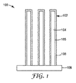
図1を参照すると、基材108上の、本明細書で説明される例示的な触媒100は、式PtxNiyIrzを有する触媒材料106によって少なくとも部分的に被覆された外表面105を有するマイクロ構造化ウィスカー104を伴うナノ構造化要素102を有し、xは26.6〜47.8の範囲内であり、yは48.7〜70の範囲内であり、zは1〜11.4の範囲内である(一部の実施形態では、xは26.6〜47.6の範囲内であり、yは48.7〜69.3の範囲内であり、zは1〜11.4の範囲内であり、xは26.6〜30の範囲内であり、yは17〜62の範囲内であり、zは1〜11.4の範囲内であり、又は更には、xは47.6〜47.8の範囲内であり、yは48.7〜52.2の範囲内であり、zは0〜3.7の範囲内であり、又は更には、1つの例示的な実施形態では、xは28.1であり、yは64.9であり、zは7.0である)。
[Mode for Carrying Out the Invention]
Referring to FIG. 1, an
適したウィスカーは、米国特許第4,812,352号(Debe)、第5,039,561号(Debe)、第5,338,430号(Parsonage et al.)、第6,136,412号(Spiewak et al.)、及び第7,419,741号(Vernstrom et al.)で説明されているものを含む、当技術分野で知られている技法により準備され得るものであり、それらの文献の開示は、参照により本明細書に組み込まれている。一般的に、ナノ構造化ウィスカーは、例えば、基材(例えば、マイクロ構造化触媒転写ポリマーシート)上に、有機又は無機材料の層を(例えば、昇華により)真空堆積させ、次いで、ペリレンレッド堆積の事例では、熱アニーリングによりペリレンレッド顔料をナノ構造化ウィスカーへと変換することにより準備され得る。典型的には、真空堆積工程は、約10−3トル又は0.1パスカル以下の全圧で実行される。例示的なマイクロ構造は、有機顔料C.I.ピグメントレッド149(すなわち、N,N’−ジ(3,5−キシリル)ペリレン−3,4:9,10−ビス(ジカルボキシイミド))の熱昇華及び真空アニーリングにより製造される。有機ナノ構造化層の製造方法は、例えば、Materials Science and Engineering,A158(1992),pp.1〜6;J.Vac.Sci.Technol.A,5,(4),July/August 1987,pp.1914〜16;J.Vac.Sci.Technol.A,6,(3),May/August 1988,pp.1907〜11;Thin Solid Films,186,1990,pp.327〜47;J.Mat.Sci.,25,1990,pp.5257〜68;Rapidly Quenched Metals,Proc.of the Fifth Int.Conf.on Rapidly Quenched Metals,Wurzburg,Germany(Sep.3〜7,1984),S.Steeb et al.,eds.,Elsevier Science Publishers B.V.,New York,(1985),pp.1117〜24;Photo.Sci.and Eng.,24,(4),July/August 1980,pp.211〜16;並びに、米国特許第4,340,276号(Maffitt et al.)及び第4,568,598号(Bilkadi et al.)で報告されており、それらの文献の開示は、参照により本明細書に組み込まれている。カーボンナノチューブアレイを使用する触媒層の特質は、論文「High Dispersion and Electrocatalytic Properties of Platinum on Well−Aligned Carbon Nanotube Arrays」,Carbon,42,(2004),pp.191〜197で報告されている。草のような(grassy)又は逆立った(bristled)ケイ素を使用する触媒層の特質は、例えば、米国特許出願公開第2004/0048466(A1)号(Gore et al.)で報告されている。 Suitable whiskers are disclosed in US Pat. Nos. 4,812,352 (Debe), 5,039,561 (Debe), 5,338,430 (Parsonage et al.), 6,136,412. (Spiewak et al.), And 7,419,741 (Vernstrom et al.), Which can be prepared by techniques known in the art, and their references. The disclosure of which is incorporated herein by reference. In general, nanostructured whiskers, for example, vacuum deposit (eg, by sublimation) a layer of organic or inorganic material onto a substrate (eg, a microstructured catalyst transfer polymer sheet) and then perylene red deposition. In this case, it can be prepared by converting perylene red pigment into nanostructured whiskers by thermal annealing. Typically, the vacuum deposition process is performed at a total pressure of about 10-3 Torr or 0.1 Pascal or less. Exemplary microstructures include organic pigments C.I. I. Pigment Red 149 (ie, N, N′-di (3,5-xylyl) perylene-3,4: 9,10-bis (dicarboximide)) is produced by thermal sublimation and vacuum annealing. The method for producing the organic nanostructured layer is described in, for example, Materials Science and Engineering, A158 (1992), pp. 1-6; Vac. Sci. Technol. A, 5, (4), July / August 1987, pp. 1914-16; Vac. Sci. Technol. A, 6, (3), May / August 1988, pp. 1907-11; Thin Solid Films, 186, 1990, pp. 327-47; Mat. Sci. , 25, 1990, pp. 5257-68; Rapidly Quenched Metals, Proc. of the First Int. Conf. on Rapidly Quenched Metals, Wurzburg, Germany (Sep. 3-7, 1984), S. et al. Steelb et al. , Eds. Elsevier Sciences Publishers B. V. , New York, (1985), pp. 1117-24; Photo. Sci. and Eng. , 24, (4), July / August 1980, pp. And U.S. Pat. Nos. 4,340,276 (Maffitt et al.) And 4,568,598 (Bilkadi et al.), The disclosures of which are incorporated by reference. Is incorporated herein. The nature of the catalyst layer using carbon nanotube arrays is described in the article “High Dispersion and Electrocatalytic Properties of Platinum on Well-Aligned Carbon Nanotube Arrays”, Carbon, 42, (2004), p. 191-197. The nature of catalyst layers using grassy or bristled silicon is reported, for example, in US Patent Application Publication No. 2004/0048466 (A1) (Gore et al.).
真空堆積は、任意の適した装置で実行され得る(例えば、米国特許第5,338,430号(Parsonage et al.)、第5,879,827号(Debe et al.)、第5,879,828号(Debe et al.)、第6,040,077号(Debe et al.)、及び第6,319,293号(Debe et al.)、並びに、米国特許出願公開第2002/0004453(A1)号(Haugen et al.)が参照され、それらの文献の開示は、参照により本明細書に組み込まれている。)1つの例示的な装置が、米国特許第5,338,430号(Parsonage et al.)の図4Aで概略的に図示され、付随するテキストで論考されており、そこでは、基材がドラム上に装着され、そのドラムは、次いで、有機前駆体(例えば、ペリレンレッド顔料)を堆積させるために昇華又は蒸発源の上方で回転させられることが、ウィスカーを形成するためにこの有機前駆体をアニーリングするより前に行われる。 Vacuum deposition can be performed in any suitable apparatus (eg, US Pat. No. 5,338,430 (Parsonage et al.), 5,879,827 (Debe et al.), 5,879). , 828 (Debe et al.), 6,040,077 (Debe et al.), And 6,319,293 (Debe et al.), And US Patent Application Publication No. 2002/0004453 ( A1) (Haugen et al.), The disclosures of which are incorporated herein by reference.) One exemplary apparatus is described in US Pat. No. 5,338,430 ( Parsonage et al.), Schematically illustrated in FIG. 4A and discussed in the accompanying text, where the substrate is mounted on a drum and The drum is then rotated over a sublimation or evaporation source to deposit an organic precursor (eg, perylene red pigment) before annealing the organic precursor to form whiskers. Done.
典型的には、堆積させられるペリレンレッド顔料の公称厚は、約50nm〜500nmの範囲内である。典型的には、ウィスカーは、20nm〜60nmの範囲内の平均断面寸法、及び、0.3マイクロメートル〜3マイクロメートルの範囲内の平均長さを有する。 Typically, the nominal thickness of the deposited perylene red pigment is in the range of about 50 nm to 500 nm. Typically, whiskers have an average cross-sectional dimension in the range of 20 nm to 60 nm and an average length in the range of 0.3 micrometers to 3 micrometers.
一部の実施形態では、ウィスカーはバッキングに取り付けられる。例示的なバッキングとしては、ポリイミド、ナイロン、金属箔、又は、最高で300℃の熱アニーリング温度に耐えることができる他の材料が挙げられる。一部の実施形態では、バッキングは、25マイクロメートル〜125マイクロメートルの範囲内の平均厚を有する。 In some embodiments, the whiskers are attached to the backing. Exemplary backings include polyimide, nylon, metal foil, or other materials that can withstand a thermal annealing temperature of up to 300 ° C. In some embodiments, the backing has an average thickness in the range of 25 micrometers to 125 micrometers.
一部の実施形態では、バッキングは、その表面のうちの少なくとも1つの上にマイクロ構造を有する。一部の実施形態では、マイクロ構造は、ウィスカーの平均サイズの少なくとも3倍(一部の実施形態では、少なくとも4倍、5倍、10倍以上)の、実質的に一様に形状設定されサイズ設定される特徴部から構成される。マイクロ構造の形状は、例えば、V字状の溝部及び頂部(例えば、米国特許第6,136,412号(Spiewak et al.)が参照され、その文献の開示は参照により本明細書に組み込まれている)、又は、角錐(例えば、米国特許第7,901,829号(Debe et al.)が参照され、その文献の開示は参照により本明細書に組み込まれている)であり得る。一部の実施形態では、31個ごとのV溝部頂部が、両側のものより25%、又は50%、又は更には100%丈長であるなどの、周期的な方式で、マイクロ構造特徴部の、ある程度の割合が、マイクロ構造化頂部の平均又は大部分より上に延びていた。一部の実施形態では、マイクロ構造化頂部の大部分より上に延びる、特徴部のこの割合は、最高で10%(一部の実施形態では、最高で3%、2%、又は更には、最高で1%)であり得る。時折より丈長のマイクロ構造特徴部の使用は、被覆された基材がロールツーロール被覆作業でローラの表面の上方を移動するとき、一様により小さいマイクロ構造頂部を保護することを助けることができる。より小さいマイクロ構造の頂部ではなく、時折より丈長の特徴部がローラの表面に触れ、そのため、ナノ構造化材料又はウィスカー材料のうち、基材が被覆プロセスを通って移動する際に、掻き取られるか又は他の形で乱される公算が大きいものは、はるかに少ない。一部の実施形態では、マイクロ構造特徴部は、実質的には、膜電極接合体を製造するにあたり触媒が転写されることになる膜の厚さの半分より小さい。このことは、触媒転写プロセス中に、より丈長のマイクロ構造特徴部が、それらの特徴部が膜の反対の側で電極と重なり合うことがある場合に、膜を貫通しないようにするためである。一部の実施形態では、最も丈長のマイクロ構造特徴部は、膜厚の1/3又は1/4未満である。最も薄いイオン交換膜(例えば、厚さで約10マイクロメートル〜15マイクロメートル)に関しては、約3マイクロメートル〜4.5マイクロメートル以下の丈長であるマイクロ構造化特徴部を伴う基材を有することが望ましいことがある。V字状の、又は他のマイクロ構造化特徴部の側部の急峻さ、すなわち、隣接する特徴部同士の間の夾角は、一部の実施形態では、積層転写プロセス中の触媒転写においての容易さのために、及び、基材バッキングの平面的な幾何学的表面に関して、2の平方根(1.414)倍のマイクロ構造化層の表面積から生じる電極の表面積の増加を生むために、90°の程度であるのが望ましいことがある。 In some embodiments, the backing has a microstructure on at least one of its surfaces. In some embodiments, the microstructure is substantially uniformly shaped and sized at least 3 times the average size of the whiskers (in some embodiments, at least 4 times, 5 times, 10 times or more). Consists of set features. For example, reference is made to V-shaped grooves and tops (eg, US Pat. No. 6,136,412 (Spiewak et al.)), The disclosure of which is incorporated herein by reference. Or a pyramid (see, eg, US Pat. No. 7,901,829 (Debe et al.), The disclosure of which is incorporated herein by reference). In some embodiments, every thirty-one V-groove top is 25%, 50%, or even 100% taller than that on both sides, in a periodic manner, such as in a microscopic feature. A certain percentage extended above the average or most of the microstructured top. In some embodiments, this percentage of features extending above most of the microstructured top can be up to 10% (in some embodiments, up to 3%, 2%, or even Up to 1%). Occasionally the use of a longer structural feature helps to protect the uniformly smaller microstructure top as the coated substrate moves over the surface of the roller in a roll-to-roll coating operation. it can. Rather than the top of the smaller microstructures, occasionally a longer feature touches the surface of the roller, so scraping of the nanostructured or whisker material as the substrate moves through the coating process Much less likely to be played or otherwise disturbed. In some embodiments, the microstructure features are substantially less than half the thickness of the membrane to which the catalyst will be transferred in making the membrane electrode assembly. This is so that during the catalyst transfer process, the longer microstructured features do not penetrate the membrane if they may overlap the electrode on the opposite side of the membrane. . In some embodiments, the tallest microstructure feature is less than 1/3 or less than 1/4 of the film thickness. For thinnest ion exchange membranes (eg, about 10 to 15 micrometers in thickness), it has a substrate with microstructured features that are about 3 to 4.5 micrometers tall It may be desirable. The steepness of the sides of V-shaped or other microstructured features, i.e., the included angle between adjacent features, in some embodiments, is easy in catalyst transfer during a laminate transfer process. And to produce an increase in the surface area of the electrode resulting from the surface area of the microstructured layer 2 times the square root (1.414) times the planar geometric surface of the substrate backing. It may be desirable to be on the order.
一部の実施形態では、触媒材料は、白金及びニッケルを含む層と、白金及びニッケルを含む層上のイリジウムを含む層とを含む。 In some embodiments, the catalyst material includes a layer comprising platinum and nickel and a layer comprising iridium over the layer comprising platinum and nickel.
一部の実施形態では、白金及びニッケルを含む層は、0.4nm〜70nmの範囲内の(一部の実施形態では、0.4nm〜10nm、0.4nm〜5nm、1nm〜25nm、又は更には、1nm〜10nmの範囲内の)平面等価厚(planar equivalent thickness)を有し、イリジウムを含む層は、0.01nm〜20nmの範囲内の(一部の実施形態では、0.01nm〜10nm、0.01nm〜5nm、0.02nm〜2.5nm、又は更には、0.02nm〜1nmの範囲内の)平面等価厚(すなわち、実質的に平坦な、平面的な基材上に堆積させられる場合の厚さ)を有する。一部の実施形態では、白金及びニッケルを集合的に含む層は、最高で600nmの(一部の実施形態では、最高で575nm、550nm、500nm、400nm、300nm、200nm、100nm、75nm、50nm、25nm、10nm、5nm、2.5nm、1nm、又は更には、最高で2つの単層(例えば、0.4nm)の、一部の実施形態では、0.4nm〜600nm、0.4nm〜500nm、1nm〜500nm、5nm〜500nm、10nm〜500nm、10nm〜400nm、又は更には、40nm〜300nmの範囲内の)平面等価厚を有し、イリジウムを含む層は、最高で50nmの(一部の実施形態では、最高で45nm、40nm、35nm、30nm、25nm、20nm、15nm、10nm、5nm、4nm、3nm、2nm、1nm、単層(例えば、0.2nm)、又は更には、単層未満(例えば、0.01nm)の、一部の実施形態では、0.01nm〜50nm、1nm〜50nm、5nm〜40nm、又は更には、5nm〜35nmの範囲内の)平面等価厚を有する。 In some embodiments, the layer comprising platinum and nickel is in the range of 0.4 nm to 70 nm (in some embodiments, 0.4 nm to 10 nm, 0.4 nm to 5 nm, 1 nm to 25 nm, or even Has a planar equivalent thickness (in the range of 1 nm to 10 nm) and the iridium-containing layer is in the range of 0.01 nm to 20 nm (in some embodiments, 0.01 nm to 10 nm). , 0.01 nm to 5 nm, 0.02 nm to 2.5 nm, or even within the range of 0.02 nm to 1 nm) equivalent planar thickness (ie, deposited on a substantially flat, planar substrate) Thickness). In some embodiments, the layer comprising platinum and nickel collectively is up to 600 nm (in some embodiments, up to 575 nm, 550 nm, 500 nm, 400 nm, 300 nm, 200 nm, 100 nm, 75 nm, 50 nm, 25 nm, 10 nm, 5 nm, 2.5 nm, 1 nm, or even up to two monolayers (eg, 0.4 nm), in some embodiments, 0.4 nm to 600 nm, 0.4 nm to 500 nm, Layers having a planar equivalent thickness (in the range of 1 nm to 500 nm, 5 nm to 500 nm, 10 nm to 500 nm, 10 nm to 400 nm, or even 40 nm to 300 nm) and containing iridium can be up to 50 nm (some implementations) In form, up to 45 nm, 40 nm, 35 nm, 30 nm, 25 nm, 20 nm, 15 nm, 10 nm 5 nm, 4 nm, 3 nm, 2 nm, 1 nm, single layer (eg, 0.2 nm), or even less than a single layer (eg, 0.01 nm), in some embodiments, 0.01 nm to 50 nm, 1 nm A planar equivalent thickness (in the range of ˜50 nm, 5 nm to 40 nm, or even 5 nm to 35 nm).
一部の実施形態では、触媒材料は、白金及びニッケルを含む交互層と、イリジウムを含む層とを(すなわち、白金及びニッケルを含む層と、イリジウムを含む層と、白金及びニッケルを含む層と、イリジウムを含む層と、等々を)含む。一部の実施形態では、少なくとも2、3、4、5、10、15、20、25、50、75、100、150、200、250個の、又は更には、少なくとも275個のセットの交互層である。 In some embodiments, the catalyst material comprises alternating layers comprising platinum and nickel and layers comprising iridium (ie, layers comprising platinum and nickel, layers comprising iridium, and layers comprising platinum and nickel). Iridium-containing layer, and so on). In some embodiments, at least 2, 3, 4, 5, 10, 15, 20, 25, 50, 75, 100, 150, 200, 250, or even at least 275 sets of alternating layers It is.
個々の堆積させられる触媒層の厚さは、例えば、層の面触媒担持量、及び触媒密度に依存し得る。例えば、平面的な基材上に堆積させられる、cm2の平面面積当たり10マイクログラムのPt、及び、21.45g/cm3の密度による、Ptの単一層の厚さは、4.7nmと算出され、同じ面積担持量によるNi層の厚さは、11.2nmである。 The thickness of the individual deposited catalyst layers can depend, for example, on the surface catalyst loading of the layer and the catalyst density. For example, with a density of 10 micrograms Pt per cm 2 planar area and a density of 21.45 g / cm 3 deposited on a planar substrate, the thickness of a single layer of Pt is 4.7 nm The thickness of the Ni layer calculated and having the same area loading is 11.2 nm.
一部の実施形態では、触媒材料は、白金を含む層と、白金を含む層上のニッケルを含む層と、ニッケルを含む層上のイリジウムを含む層とを含む。一部の実施形態では、触媒材料は、ニッケルを含む層と、ニッケルを含む層上の白金を含む層と、白金を含む層上のイリジウムを含む層とを含む。一部の実施形態では、触媒材料は、白金、ニッケル、及びイリジウムの、順次繰り返す個々の層を含む。一部の実施形態では、少なくとも2、3、4、5、10、15、20、25、50、75、100、150、200、250個の、又は更には、少なくとも275個のセットの繰り返す層である。 In some embodiments, the catalyst material includes a layer that includes platinum, a layer that includes nickel on the layer that includes platinum, and a layer that includes iridium on the layer that includes nickel. In some embodiments, the catalyst material includes a layer that includes nickel, a layer that includes platinum on the layer that includes nickel, and a layer that includes iridium on the layer that includes platinum. In some embodiments, the catalyst material comprises sequentially repeating individual layers of platinum, nickel, and iridium. In some embodiments, at least 2, 3, 4, 5, 10, 15, 20, 25, 50, 75, 100, 150, 200, 250, or even at least 275 sets of repeating layers. It is.
一部の実施形態では、触媒材料は、露出したイリジウム表面層を有する。 In some embodiments, the catalyst material has an exposed iridium surface layer.
一部の実施形態では、各々の層は、最高で100nmの(一部の実施形態では、最高で50nm、20nm、15nm、10nm、5nm、4nm、3nm、2nm、1nm、単層(例えば、0.2nm)、又は更には、最高で単層未満(例えば、0.01nm)の、一部の実施形態では、0.01nm〜100nm、0.01nm〜50nm、0.1nm〜15nm、0.1nm〜10nm、又は更には、1nm〜5nmの範囲内の)平面等価厚をそれぞれ独立して有する。 In some embodiments, each layer is up to 100 nm (in some embodiments, up to 50 nm, 20 nm, 15 nm, 10 nm, 5 nm, 4 nm, 3 nm, 2 nm, 1 nm, single layer (e.g., 0 .2 nm), or even up to less than a single layer (e.g., 0.01 nm), in some embodiments, 0.01 nm to 100 nm, 0.01 nm to 50 nm, 0.1 nm to 15 nm, 0.1 nm Each having a plane equivalent thickness (in the range of 10 nm to 10 nm, or even 1 nm to 5 nm) independently.
一般的に、触媒は、当技術分野で知られている技法により堆積させられ得る。例示的な堆積技法としては、スパッタリング(反応性スパッタリングを含む)、原子層堆積、分子有機化学蒸着、分子線エピタキシー、熱物理蒸着、エレクトロスプレーイオン化による真空堆積、及びパルスレーザ堆積からなる群から独立して選択されるものが挙げられる。追加的な一般的な詳細は、例えば、米国特許第5,879,827号(Debe et al.)、第6,040,077号(Debe et al.)、及び第7,419,741号(Vernstrom et al.)で見出され得るものであり、それらの文献の開示は、参照により本明細書に組み込まれている。熱物理蒸着法は、(例えば、抵抗加熱、電子ビーム銃、又はレーザによる)適した昇温を使用して、ターゲット(原料材料)を蒸気状態へと融解又は昇華させ、その蒸気状態のものが、真空空間を通過させられ、次いでその熱物理蒸着法は、この蒸発させられた形態のものを基材表面上に凝縮させる。熱物理蒸着機器は、例えば、それぞれ、「METAL EVAPORATOR(ME−SERIES)」又は「ORGANIC MOLECULAR EVAPORATOR(DE−SERIES)」という商品名で、独国ドレスデンのCreaPhys GmbHから、金属蒸発器として、又は有機分子蒸発器として入手可能なものを含めて、当技術分野で知られており、別の例の有機材料蒸発器は、「ORGANIC MATERIALS EVAPORATIOR(ORMA−SERIES)」という商品名で、英国オックスフォードシャーのMantis Deposition LTDから入手可能である。複数個の交互層を含む触媒材料は、例えば、複数個のターゲットからスパッタリングされ得る(例えば、Ptが第1のターゲットからスパッタリングされ、Niが第2のターゲットからスパッタリングされ、Irが、第3のものから、又は、2つ以上の元素(例えば、Pt及びNi)を含むターゲットからである)。触媒被覆が、単一ターゲットによって行われる場合、触媒被覆の凝縮の熱が、下方にある触媒、該当する際のPt、Ni、又はIr原子、及び基材表面を加熱することを、これらの原子が、良好に混合され、熱力学的に安定な合金ドメインを形成するのに充分な表面移動性をもたらすのに十分に行うように、被覆層が、単一の工程で、ガス分配層、ガス分散層、触媒転写層、又は膜上に付与されるということが望ましいことがある。あるいは、例えば、基材は更には、この原子移動性を促進するために、熱い様態で準備され得る、又は加熱され得る。一部の実施形態では、スパッタリングは、アルゴンを含む雰囲気中で、少なくとも部分的に遂行される。有機金属形態の触媒は、例えば、質量選別されたイオンのソフト又は反応性ランディングにより堆積させられ得る。質量選別されたイオンのソフトランディングは、有機配位子を完備した触媒活性金属錯体を、この気相から不活性表面上に移転させるために使用される。この方法は、画定された活性部位を伴う材料を調製するために使用され得るものであり、かくして、周囲条件、又は、伝統的な真空条件のいずれかのもとで、高度に制御された様式で、表面の分子設計を達成することができる。追加的な詳細に関しては、例えば、Johnson et al.,Anal.Chem.,2010,82,pp.5718〜5727、及び、Johnson et al.,Chemistry:A European Journal,2010,16,pp.14433〜14438が参照され、それらの文献の開示は、参照により本明細書に組み込まれている。 In general, the catalyst can be deposited by techniques known in the art. Exemplary deposition techniques are independent of the group consisting of sputtering (including reactive sputtering), atomic layer deposition, molecular organic chemical vapor deposition, molecular beam epitaxy, thermal physical vapor deposition, vacuum deposition by electrospray ionization, and pulsed laser deposition. Can be selected. Additional general details can be found, for example, in US Pat. Nos. 5,879,827 (Debe et al.), 6,040,077 (Debe et al.), And 7,419,741 ( Vernstrom et al.), The disclosures of which are incorporated herein by reference. Thermal physical vapor deposition uses a suitable temperature rise (eg, by resistance heating, an electron beam gun, or a laser) to melt or sublimate the target (raw material) into a vapor state, , Passed through a vacuum space, and then the thermal physical vapor deposition condenses this evaporated form onto the substrate surface. Thermophysical vapor deposition equipment, for example, under the trade name “METAL EVAROTOROR (ME-SERIES)” or “ORGANIC MOOLECULAR EVAPORATOR (DE-SERIES)”, respectively, from CreatPhys GmbH, Dresden, Germany, as an organic evaporator or organic Another example of an organic material evaporator known in the art, including what is available as a molecular evaporator, is an organic material evaporator under the trade name "ORGANIC MATERIALS EVAPORATOR (ORMA-SERIES)" in Oxfordshire, England. Available from Mantis Deposition LTD. The catalyst material comprising a plurality of alternating layers can be sputtered, for example, from a plurality of targets (eg, Pt is sputtered from the first target, Ni is sputtered from the second target, Ir is the third, Or from a target containing two or more elements (eg, Pt and Ni)). If the catalyst coating is performed by a single target, the heat of condensation of the catalyst coating will heat the underlying catalyst, the Pt, Ni, or Ir atoms as applicable, and the substrate surface. In a single step so that the coating layer is sufficient to provide sufficient surface mobility to form a well-mixed and thermodynamically stable alloy domain. It may be desirable to be applied on the dispersion layer, the catalyst transfer layer, or the membrane. Alternatively, for example, the substrate can be further prepared in a hot manner or heated to promote this atom mobility. In some embodiments, sputtering is performed at least partially in an atmosphere comprising argon. The organometallic form of the catalyst can be deposited, for example, by soft or reactive landing of mass sorted ions. Soft landing of mass-selected ions is used to transfer catalytically active metal complexes complete with organic ligands from this gas phase onto an inert surface. This method can be used to prepare materials with defined active sites, and thus in a highly controlled manner under either ambient conditions or traditional vacuum conditions. Thus, the molecular design of the surface can be achieved. For additional details, see, for example, Johnson et al. , Anal. Chem. , 2010, 82, pp. 5718-5727, and Johnson et al. , Chemistry: A European Journal, 2010, 16, pp. 14433-14438, the disclosures of which are incorporated herein by reference.
一部の実施形態では、白金のイリジウムに対する重量比は、1:1〜50:1の範囲内(一部の実施形態では、2:1〜40:1の範囲内)である。 In some embodiments, the weight ratio of platinum to iridium is in the range of 1: 1 to 50: 1 (in some embodiments, in the range of 2: 1 to 40: 1).
一部の実施形態では、本明細書で説明される触媒の製造方法は、白金及びニッケルを含むターゲット(例えば、Pt3Ni7ターゲット)から白金及びニッケルを堆積させることと、イリジウムを含むターゲットからイリジウムを堆積させることと、を含む。一部の実施形態では、白金及びニッケルを含む層は、0.4nm〜580nmの範囲内の(一部の実施形態では、0.4nm〜72nmの範囲内の)平面等価厚を有し、イリジウムを含む層は、0.01nm〜32nmの範囲内の(一部の実施形態では、0.01nm〜16nmの範囲、又は更には、0.01nm〜2nmの範囲内の)平面等価厚を有する。 In some embodiments, the method of making a catalyst described herein includes depositing platinum and nickel from a target including platinum and nickel (eg, a Pt 3 Ni 7 target) and from a target including iridium. Depositing iridium. In some embodiments, the layer comprising platinum and nickel has a planar equivalent thickness in the range of 0.4 nm to 580 nm (in some embodiments, in the range of 0.4 nm to 72 nm), and iridium The layer comprising has a planar equivalent thickness in the range of 0.01 nm to 32 nm (in some embodiments, in the range of 0.01 nm to 16 nm, or even in the range of 0.01 nm to 2 nm).
一部の実施形態では、本明細書で説明される触媒の製造方法は、白金を含むターゲットから白金を堆積させることと、ニッケルを含むターゲットからニッケルを堆積させることと、イリジウムを含むターゲットからイリジウムを堆積させることと、を含む。一部の実施形態では、白金を含む層、ニッケルを含む隣接層、及び、イリジウムを含む隣接層は、0.5nm〜50nmの範囲内の(一部の実施形態では、0.5nm〜30nmの範囲内の)集合的な平面等価厚を有する。一部の実施形態では、白金を含む層は、0.2nm〜30nmの範囲内の(一部の実施形態では、0.2nm〜20nm、又は更には、0.2nm〜10nmの範囲内の)平面等価厚を有し、ニッケルを含む層は、0.2nm〜50nmの範囲内の(一部の実施形態では、0.2nm〜25nm、又は更には、0.2nm〜10nmの範囲内の)平面等価厚を有し、イリジウムを含む層は、0.01nm〜20nmの範囲内の(一部の実施形態では、0.01nm〜10nm、0.01nm〜5nm、0.02nm〜5nm、0.02nm〜1nm、又は更には、0.1nm〜1nmの範囲内の)平面等価厚を有する。一部の実施形態では、白金のイリジウムに対する重量比は、2.4:1〜34.3:1の範囲内(一部の実施形態では、6.5:1〜34.3:1、又は更には、9.7:1〜34.3:1の範囲内)である。 In some embodiments, a method of making a catalyst described herein includes depositing platinum from a target that includes platinum, depositing nickel from a target that includes nickel, and iridium from a target that includes iridium. Depositing. In some embodiments, the platinum-containing layer, the nickel-containing adjacent layer, and the iridium-containing adjacent layer are in the range of 0.5 nm to 50 nm (in some embodiments, 0.5 nm to 30 nm). Have a collective planar equivalent thickness (within range). In some embodiments, the layer comprising platinum is in the range of 0.2 nm to 30 nm (in some embodiments, in the range of 0.2 nm to 20 nm, or even 0.2 nm to 10 nm). The layer having a planar equivalent thickness and comprising nickel is in the range of 0.2 nm to 50 nm (in some embodiments, in the range of 0.2 nm to 25 nm, or even 0.2 nm to 10 nm). The layer having a planar equivalent thickness and containing iridium is in the range of 0.01 nm to 20 nm (in some embodiments, 0.01 nm to 10 nm, 0.01 nm to 5 nm, 0.02 nm to 5 nm,. It has a planar equivalent thickness (in the range of 02 nm to 1 nm, or even 0.1 nm to 1 nm). In some embodiments, the weight ratio of platinum to iridium is in the range of 2.4: 1 to 34.3: 1 (in some embodiments, 6.5: 1 to 34.3: 1, or Furthermore, it is in the range of 9.7: 1 to 34.3: 1).
一部の実施形態では、白金及びニッケルを含む少なくとも1つの層(白金及びニッケルを含む層、又は、白金、ニッケル、及びイリジウムを含む層を含む)はナノ多孔質(例えば、1nm〜10nmの範囲内の(一部の実施形態では、2nm〜8nm、又は更には、3nm〜7nmの範囲内の)直径を伴う細孔)である。一部の実施形態では、白金及びニッケルを含む、少なくとも2、3、4、5、10、15、20、25、50、75、100、150、200、250個の、又は更には、少なくとも275個の層がナノ多孔質である。 In some embodiments, at least one layer comprising platinum and nickel (including a layer comprising platinum and nickel or a layer comprising platinum, nickel, and iridium) is nanoporous (eg, in the range of 1 nm to 10 nm). Pores with diameters (in some embodiments, in the range of 2 nm to 8 nm, or even 3 nm to 7 nm). In some embodiments, at least 2, 3, 4, 5, 10, 15, 20, 25, 50, 75, 100, 150, 200, 250, or even at least 275, including platinum and nickel. The individual layers are nanoporous.
ナノ多孔性は、触媒材料を脱合金化して、ニッケルの一部分を除去することにより準備され得る。一般的に、脱合金化は、「自由腐食」手法(例えば、酸中の浸漬)によること、又は、電気化学的処理(例えば、酸性媒体での電位サイクリング)によることを含む、当技術分野で知られている技法により成し遂げられ得る。ナノ多孔性形成は、典型的には、脱合金化媒体での十分に異なる溶解速度を伴う少なくとも2つの成分を含む合金で、及び、より腐食しない成分が、十分な表面移動性を有するときに発生する。追加的な詳細に関しては、例えば、Erlebacher et al.,Nature,2001,410,pp.450〜453、並びに、米国特許第6,805,972(B2)号(Erlebacher et al.);第8,673,773(B2)号(Opperman et al.);及び第8,895,206(B2)号(Erlebacher et al.)が参照され、それらの文献の開示は参照により本明細書に組み込まれている。 Nanoporosity can be prepared by dealloying the catalyst material to remove a portion of the nickel. In general, dealloying is known in the art, including by “free corrosion” techniques (eg, immersion in acid) or by electrochemical treatment (eg, potential cycling in acidic media). Can be accomplished by known techniques. Nanoporosity is typically an alloy containing at least two components with sufficiently different dissolution rates in a dealloying medium, and when a less corrosive component has sufficient surface mobility. Occur. For additional details, see, for example, Erlebacher et al. , Nature, 2001, 410, pp. 450-453, and U.S. Patent Nos. 6,805,972 (B2) (Errebacher et al.); 8,673,773 (B2) (Operman et al.); And 8,895,206 ( No. B2) (Errebacher et al.), The disclosures of which are incorporated herein by reference.
一部の実施形態では、触媒材料はアニーリングされる。一部の実施形態では、触媒は、脱合金化の前にアニーリングされる。一般的に、アニーリングは、触媒材料を、例えばオーブン又はファーネスによって、レーザによって、及び、赤外線技法によって加熱することを含む、当技術分野で知られている技法により行われ得る。アニーリングは、例えば、不活性又は反応性ガス環境で遂行され得る。理論により束縛されることを欲してはいないが、アニーリングは、触媒の活性及び耐久性に影響を及ぼし得る、原子スケールでの構造的変化を誘導することができると考えられる。更に、ナノスケール粒子及びフィルムをアニーリングすることは、粒子又は薄フィルムグレインの成長を引き起こし得る、原子構成成分での移動性を誘導することができると考えられる。多元素混合物、合金、又は、層状粒子及びフィルムの事例では、アニーリングは、例えば、成分元素特質及びアニーリング環境に依存して、表面に対する粒子又はフィルムの中の成分の偏析、ランダムの不規則合金の形成、及び、規則的な金属間化合物の形成を誘導することができると考えられる。アニーリングについての追加的な詳細に関しては、例えば、van der Vliet et al.,Nature Materials,2012,11,pp.1051〜1058;Wang et al.,Nature Materials,2013,12,pp.81〜87、及び、米国特許第8,748,330(B2)号(Debe et al.)が参照され、それらの文献の開示は参照により本明細書に組み込まれている。 In some embodiments, the catalyst material is annealed. In some embodiments, the catalyst is annealed prior to dealloying. In general, annealing may be performed by techniques known in the art, including heating the catalyst material, for example, by an oven or furnace, by a laser, and by infrared techniques. Annealing can be performed, for example, in an inert or reactive gas environment. While not wishing to be bound by theory, it is believed that annealing can induce structural changes at the atomic scale that can affect the activity and durability of the catalyst. Furthermore, it is believed that annealing nanoscale particles and films can induce mobility at atomic components that can cause the growth of particles or thin film grains. In the case of multi-element mixtures, alloys, or layered particles and films, annealing is dependent on, for example, component element characteristics and the annealing environment, segregation of the components in the particles or film to the surface, random disordered alloys It is believed that formation and regular intermetallic compound formation can be induced. For additional details on annealing, see, for example, van der Vliet et al. , Nature Materials, 2012, 11, pp. 1051-1058; Wang et al. , Nature Materials, 2013, 12, pp. 81-87 and US Pat. No. 8,748,330 (B2) (Debe et al.), The disclosures of which are incorporated herein by reference.
一部の実施形態では、本明細書で説明される触媒の製造方法は、
白金及びニッケルを含むターゲットから白金及びニッケルを堆積させて、白金及びニッケルを含む少なくとも1つの層を準備すること(一部の実施形態では、ターゲットから繰り返し堆積させて、複数個の層を準備すること)と、
白金及びニッケルを含む少なくとも1つの層を脱合金化して、少なくとも1つの層からニッケルを除去することと、
イリジウムを含むターゲットからイリジウムを含む層を堆積させることと、を含む。一部の実施形態では、ニッケルが除去された、1nm〜10nmの範囲内の(一部の実施形態では、2nm〜8nm、又は更には、3nm〜7nmの範囲内の)直径を伴う細孔が存する。一部の実施形態では、ターゲットはPt3Ni7ターゲットである。
In some embodiments, the method for producing a catalyst described herein comprises:
Depositing platinum and nickel from a target including platinum and nickel to prepare at least one layer including platinum and nickel (in some embodiments, repeatedly depositing from the target to prepare a plurality of layers That)
De-alloying at least one layer comprising platinum and nickel to remove nickel from the at least one layer;
Depositing a layer containing iridium from a target containing iridium. In some embodiments, pores with diameters in the range of 1 nm to 10 nm (in some embodiments in the range of 2 nm to 8 nm, or even 3 nm to 7 nm) from which nickel has been removed have been removed. Exist. In some embodiments, the target is a Pt 3 Ni 7 target.
一部の実施形態では、本明細書で説明される触媒の製造方法であって、
白金を含むターゲットから白金を堆積させて、白金を含む少なくとも1つの層を準備することと、
ニッケルを含むターゲットからニッケルを堆積させて、ニッケルを含む少なくとも1つの層を準備することと、
白金及びニッケルを含む少なくとも1つの層を脱合金化して、少なくとも1つの層からニッケルを除去することと、
イリジウムを含むターゲットからイリジウムを含む層を堆積させることと、を含む、製造方法である。一部の実施形態では、層を堆積させて、白金又はニッケルをそれぞれ含む交互層を準備することである。一部の実施形態では、ニッケルが除去された、1nm〜10nmの範囲内の(一部の実施形態では、2nm〜8nm、又は更には、3nm〜7nmの範囲内の)直径を伴う細孔が存する。
In some embodiments, a method of making a catalyst as described herein comprising:
Depositing platinum from a platinum-containing target to provide at least one layer containing platinum;
Depositing nickel from a target containing nickel to prepare at least one layer containing nickel;
De-alloying at least one layer comprising platinum and nickel to remove nickel from the at least one layer;
Depositing a layer containing iridium from a target containing iridium. In some embodiments, the layers are deposited to provide alternating layers comprising platinum or nickel, respectively. In some embodiments, pores with diameters in the range of 1 nm to 10 nm (in some embodiments in the range of 2 nm to 8 nm, or even 3 nm to 7 nm) from which nickel has been removed have been removed. Exist.
一部の実施形態では、本明細書で説明される触媒の製造方法は、
白金及びニッケルを含むターゲットから白金及びニッケルを堆積させて、白金及びニッケルを含む第1の層を準備することと、
イリジウムを含むターゲットからイリジウムを含む層を堆積させることと、
先行する2つのステップを、順に、少なくとも1回繰り返すこと(一部の実施形態では、2、3、4、5、10、15、20、25、50、75、100、150、200、250回、又は更には、少なくとも275回繰り返すこと)と、
白金及びニッケルを含む少なくとも1つの層を脱合金化して、層からニッケルを除去することと、を含む。一部の実施形態では、ニッケルが除去された、1nm〜10nmの範囲内の(一部の実施形態では、2nm〜8nm、又は更には、3nm〜7nmの範囲内の)直径を伴う細孔が存する。一部の実施形態では、ターゲットはPt3Ni7ターゲットである。
In some embodiments, the method for producing a catalyst described herein comprises:
Depositing platinum and nickel from a target comprising platinum and nickel to provide a first layer comprising platinum and nickel;
Depositing a layer containing iridium from a target containing iridium;
Repeat the preceding two steps at least once in sequence (in some
De-alloying at least one layer comprising platinum and nickel to remove nickel from the layer. In some embodiments, pores with diameters in the range of 1 nm to 10 nm (in some embodiments in the range of 2 nm to 8 nm, or even 3 nm to 7 nm) from which nickel has been removed have been removed. Exist. In some embodiments, the target is a Pt 3 Ni 7 target.
本明細書で説明される触媒は、例えば、燃料電池膜電極接合体(membrane electrode assembly、MEA)において有用である。「膜電極接合体」は、膜と、アノード及びカソード電極層と、ガス拡散層とを含む、燃料電池材料の層状サンドイッチを指す。典型的には、カソード触媒層は、本明細書で説明される触媒を含むが、一部の実施形態では、アノード触媒層は、本明細書で説明される触媒を独立して含む。 The catalysts described herein are useful, for example, in fuel cell membrane electrode assemblies (MEAs). “Membrane electrode assembly” refers to a layered sandwich of fuel cell materials comprising a membrane, anode and cathode electrode layers, and a gas diffusion layer. Typically, the cathode catalyst layer includes the catalyst described herein, but in some embodiments, the anode catalyst layer independently includes the catalyst described herein.
MEAは、順に、
第1の主表面と第2の反対側の主表面とを有する第1のガス分配層と、
第1の主表面と第2の反対側の主表面とを有するアノード触媒層であって、アノード触媒は第1の触媒を含む、アノード触媒層と、
電解質膜と、
第1の主表面と第2の反対側の主表面とを有するカソード触媒層であって、カソード触媒は第2の触媒を含む、カソード触媒層と、
第1の主表面と第2の反対側の主表面とを有する第2のガス分配層と、を含む。
The MEA is
A first gas distribution layer having a first major surface and a second opposite major surface;
An anode catalyst layer having a first major surface and a second opposite major surface, wherein the anode catalyst comprises a first catalyst;
An electrolyte membrane;
A cathode catalyst layer having a first major surface and a second opposite major surface, wherein the cathode catalyst comprises a second catalyst;
A second gas distribution layer having a first main surface and a second opposite main surface.
電解質膜は、アノード触媒層とカソード触媒層との間で反応中間体イオンを導通させる。電解質膜は、好ましくは、化学的及び電気化学的酸化安定性を含む、電気化学的環境での高い耐久性を有する。電解質膜は、好ましくは、反応中間体イオンの輸送に対する低いイオン抵抗を有するが、他のイオン、電子、及び反応物種に対しては、相対的に不透過性の障壁である。一部の実施形態では、電解質膜は、陽イオンを導通させるプロトン交換膜(proton exchange membrane、PEM)である。PEM燃料電池では、電解質膜は、好ましくは、プロトンを導通させる。PEMは、典型的には、構造的主鎖及びペンダント陽イオン交換基から構成される、部分的にフッ素化された、又は全フッ素化されたポリマーである。PEMは、例えば、「NAFION」という商品名で、デラウェア州ウィルミントンのE.I.du Pont de Nemours and Companyから、「AQUIVION」という商品名で、ベルギー国ブリュッセルのSolvayから、「3M PFSA MEMBRANE」という商品名で、ミネソタ州セントポールの3M Companyから、及び、「FLEMION」という商品名で、日本国東京の旭硝子株式会社から入手可能である。 The electrolyte membrane conducts reaction intermediate ions between the anode catalyst layer and the cathode catalyst layer. The electrolyte membrane preferably has high durability in an electrochemical environment, including chemical and electrochemical oxidative stability. The electrolyte membrane preferably has a low ionic resistance to transport of reaction intermediate ions, but is a relatively impermeable barrier to other ions, electrons, and reactant species. In some embodiments, the electrolyte membrane is a proton exchange membrane (PEM) that conducts cations. In PEM fuel cells, the electrolyte membrane preferably conducts protons. PEMs are partially fluorinated or fully fluorinated polymers that are typically composed of a structural backbone and pendant cation exchange groups. PEM, for example, under the trade name “NAFION” is an E.I. in Wilmington, Delaware. I. Du Pont de Nemours and Company under the trade name "AQUIVION", from Solvay in Brussels, Belgium, under the trade name "3M PFSA MEMBRANE", from the 3M Company in St. Paul, Minnesota, and under the trade name "FLEMION" And available from Asahi Glass Co., Ltd. in Tokyo, Japan.
ガス分配層は、一般的に、ガスを均等に電極に供給し、一部の実施形態では、電気を伝導する。そのガス分配層は、更には、燃料電池の事例では、蒸気又は液体のいずれかの形態での水の除去を可能にする。ガス分配層は、典型的には、電極と流れ場との間の反応物及び生成物輸送を可能とするように多孔質である。ガス分配層の原料は、不織紙又は織物の形態での、多孔質層を形成するようにランダムに配向された炭素繊維を含む。不織炭素紙は、例えば、「GRAFIL U−105」という商品名で、日本国東京の三菱レイヨン株式会社から、「TORAY」という商品名で、日本国東京の東レ株式会社から、「AVCARB」という商品名で、マサチューセッツ州ローウェルのAvCarb Material Solutionsから、「SIGRACET」という商品名で、独国ヴィースバーデンのSGL Group,the Carbon Companyから、「FREUDENBERG」という商品名で、独国ヴァインハイムのFreudenberg FCCT SE & Co.KG,Fuel Cell Component Technologiesから、及び、「SPECTRACARB GDL」という商品名で、コネチカット州シェルトンのEngineered Fibers Technology(EFT)から入手可能である。炭素織物又は織布は、例えば、「EC−CC1−060」及び「EC−AC−CLOTH」という商品名で、マサチューセッツ州ウーバンのElectro Chem Inc.から、「ELAT−LT」及び「ELAT」という商品名で、インディアナ州クラウンポイントのNuVant Systems Inc.から、「E−TEK ELAT LT」という商品名で、北米のBASF Fuel Cell GmbHから、並びに、「ZOLTEK CARBON CLOTH」という商品名で、ミズーリ州セントルイスのZoltek Corp.から入手可能である。不織紙又は織物は、その疎水性を修正するように処置され得る(例えば、後続の乾燥及びアニーリングを伴う、ポリテトラフルオロエチレン(polytetrafluoroethylene、PTFE)懸濁液による処置)。ガス分散層は、サブマイクロメートル電子伝導性粒子(例えば、炭素)の多孔質層と、バインダー(例えば、PTFE)とを含むことが多い。理論により束縛されることを欲してはいないが、ガス分散層は、電極とガス分配層との間の反応物及び生成物水輸送を促進するということが考えられる。 The gas distribution layer generally supplies gas evenly to the electrodes and, in some embodiments, conducts electricity. The gas distribution layer further allows the removal of water in either vapor or liquid form in the case of fuel cells. The gas distribution layer is typically porous to allow reactant and product transport between the electrode and the flow field. The raw material of the gas distribution layer includes carbon fibers randomly oriented to form a porous layer in the form of a nonwoven paper or fabric. The non-woven carbon paper is, for example, “AVAFRB” from Mitsubishi Rayon Co., Ltd. in Tokyo, Japan, “TORAY”, from Toray Co., Ltd., Tokyo, Japan, under the trade name “GRAFIL U-105”. The product name is AvCarb Material Solutions, Lowell, Massachusetts, the product name is “SIGRACE”, the product name is SGL Group, the Carbon Company, Wiesbaden, Germany, and the product name “FREEDENBERG” is from Fred, Seinen, Germany. & Co. KG, Fuel Cell Component Technologies and under the trade designation “SPECTRACARB GDL” are available from Engineered Fibers Technology (EFT), Shelton, Connecticut. Carbon fabrics or woven fabrics are, for example, trade names “EC-CC1-060” and “EC-AC-CLOTH” under the name of Electro Chem Inc. of Uban, Massachusetts. From NuVant Systems Inc. of Crown Point, Indiana under the trade designations “ELAT-LT” and “ELAT”. From the North American BASF Fuel Cell GmbH, under the trade name “E-TEK ELAT LT”, and under the trade name “ZOLTEK CARBON CLOTH”, Zoltek Corp. of St. Louis, Missouri. Is available from The nonwoven paper or fabric can be treated to modify its hydrophobicity (eg, treatment with a polytetrafluoroethylene (PTFE) suspension with subsequent drying and annealing). The gas dispersion layer often includes a porous layer of submicrometer electron conductive particles (eg, carbon) and a binder (eg, PTFE). Without wishing to be bound by theory, it is believed that the gas dispersion layer facilitates reactant and product water transport between the electrode and the gas distribution layer.
アノード触媒又はカソード触媒のうちの少なくとも1つは、本明細書で説明される触媒材料を伴うウィスカーを有する。「他の触媒層」は、当技術分野で知られている従来の触媒であってよく、当技術分野で知られている技法(例えば、米国特許第5,759,944号(Buchanan et al.)、第5,068,161号(Keck et al.)、及び第4,447,506号(Luczak et al.))により準備され得るものであり、それらの文献の開示は、参照により本明細書に組み込まれている。 At least one of the anode catalyst or cathode catalyst has a whisker with the catalyst material described herein. The “other catalyst layer” may be a conventional catalyst known in the art, and is known in the art (eg, US Pat. No. 5,759,944 (Buchan et al. ), 5,068,161 (Keck et al.), And 4,447,506 (Luczak et al.)), The disclosures of which are hereby incorporated by reference. Embedded in the book.
一部の実施形態では、カソード及び/又はアノード触媒層は、本明細書で説明される触媒材料を伴うウィスカーを含む。 In some embodiments, the cathode and / or anode catalyst layer comprises whiskers with the catalyst material described herein.
燃料電池は、水素燃料、及び、空気からの酸素を結び付けて、電気、熱、及び水を生み出す電気化学的デバイスである。燃料電池は燃焼を利用せず、しかるがゆえに、燃料電池は、有害な廃水があるとしてもほとんど生み出さない。燃料電池は、水素燃料及び酸素を直接電気へと変換し、例えば、内燃発電機よりはるかに高い効率で動作させられ得る。 A fuel cell is an electrochemical device that combines hydrogen fuel and oxygen from the air to produce electricity, heat, and water. Fuel cells do not make use of combustion, and therefore fuel cells produce little if any harmful wastewater. Fuel cells convert hydrogen fuel and oxygen directly into electricity and can be operated with much higher efficiency than, for example, internal combustion generators.
図2を参照すると、例示的な燃料電池200は、アノード203に隣接する第1のガス分配層201を含む。隣接するアノード203は、電解質膜204である。カソード205は、電解質膜204に隣接して位置し、第2のガス分配層207は、カソード205に隣接して位置する。動作時に、水素燃料は、燃料電池200のアノード部分内に導入され、第1のガス分配層201を通過し、アノード203の上方を進む。アノード203で、水素燃料は、水素イオン(H+)及び電子(e−)へと分離される。
With reference to FIG. 2, an
電解質膜204は、水素イオンすなわちプロトンのみが、電解質膜204を通過し、燃料電池200のカソード部分に進むことを許す。電子は、電解質膜204を通過することはできず、代わりに、電流の形態で外部電気回路を通って流れる。この電流は、電気モータなどの電気負荷217に電力供給することができ、又は、再充電可能バッテリなどのエネルギー貯蔵デバイスに方向付けられ得る。
The
酸素は、第2の分配層207を経て、燃料電池200のカソード側内に流れる。酸素がカソード205の上方を進む際に、酸素、プロトン、及び電子が結び付いて、水及び熱を生み出す。
例示的な実施形態
Oxygen flows into the cathode side of the
Exemplary Embodiment
1A.式PtxNiyIrzを有する触媒材料によって少なくとも部分的に被覆された外表面を有するマイクロ構造化ウィスカーを含むナノ構造化要素を含む触媒であって、xは26.6〜47.8の範囲内であり、yは48.7〜70の範囲内であり、zは1〜11.4の範囲内である(一部の実施形態では、xは26.6〜47.6の範囲内であり、yは48.7〜69.3の範囲内であり、zは1〜11.4の範囲内であり、xは26.6〜30の範囲内であり、yは17〜62の範囲内であり、zは1〜11.4の範囲内であり、又は更には、xは47.6〜47.8の範囲内であり、yは48.7〜52.2の範囲内であり、zは0〜3.7の範囲内であり、又は更には、1つの例示的な実施形態では、xは28.1であり、yは64.9であり、zは7.0である)、触媒。 1A. A catalyst comprising nanostructured elements comprising microstructured whiskers having an at least partially coated outer surface by the catalyst material having the formula Pt x Ni y Ir z, x is the 26.6 to 47.8 Is in the range, y is in the range of 48.7 to 70, and z is in the range of 1 to 11.4 (in some embodiments, x is in the range of 26.6 to 47.6. And y is in the range of 48.7 to 69.3, z is in the range of 1 to 11.4, x is in the range of 26.6 to 30, and y is in the range of 17 to 62. Is in the range, z is in the range of 1 to 11.4, or even x is in the range of 47.6 to 47.8, and y is in the range of 48.7 to 52.2. Yes, z is in the range of 0-3.7, or even in one exemplary embodiment, x is 28.1 and y is 6 A .9, z is 7.0), the catalyst.
2A.触媒材料は、白金及びニッケルを含む層と、白金及びニッケルを含む層上のイリジウムを含む層とを含む、例示的な実施形態1Aに記載の触媒。 2A. The catalyst of embodiment 1A, wherein the catalyst material comprises a layer comprising platinum and nickel and a layer comprising iridium on the layer comprising platinum and nickel.
3A.白金及びニッケルを集合的に含む層は、最高で600nmの(一部の実施形態では、最高で575nm、550nm、500nm、400nm、300nm、200nm、100nm、75nm、50nm、25nm、10nm、5nm、2.5nm、1nm、又は更には、最高で2つの単層(例えば、0.4nm)の、一部の実施形態では、0.4nm〜600nm、0.4nm〜500nm、1nm〜500nm、5nm〜500nm、10nm〜500nm、10nm〜400nm、又は更には、40nm〜300nmの範囲内の)平面等価厚を有し、イリジウムを含む層は、最高で50nmの(一部の実施形態では、最高で45nm、40nm、35nm、30nm、25nm、20nm、15nm、10nm、5nm、4nm、3nm、2nm、1nm、単層(例えば、0.2nm)、又は更には、単層未満(例えば、0.01nm)の、一部の実施形態では、0.01nm〜50nm、1nm〜50nm、5nm〜40nm、又は更には、5nm〜35nmの範囲内の)平面等価厚を有する、例示的な実施形態2Aに記載の触媒。 3A. Layers comprising platinum and nickel collectively can be up to 600 nm (in some embodiments, up to 575 nm, 550 nm, 500 nm, 400 nm, 300 nm, 200 nm, 100 nm, 75 nm, 50 nm, 25 nm, 10 nm, 5 nm, 2 nm 0.5 nm, 1 nm, or even up to two monolayers (e.g., 0.4 nm), in some embodiments, 0.4 nm-600 nm, 0.4 nm-500 nm, 1 nm-500 nm, 5 nm-500 nm Having a planar equivalent thickness in the range of 10 nm to 500 nm, 10 nm to 400 nm, or even 40 nm to 300 nm, and the layer containing iridium can be up to 50 nm (in some embodiments, up to 45 nm, 40 nm, 35 nm, 30 nm, 25 nm, 20 nm, 15 nm, 10 nm, 5 nm, 4 nm, 3 nm m, 2 nm, 1 nm, monolayer (eg, 0.2 nm), or even less than a monolayer (eg, 0.01 nm), in some embodiments, 0.01 nm-50 nm, 1 nm-50 nm, 5 nm The catalyst of exemplary embodiment 2A, having a planar equivalent thickness (in the range of ˜40 nm, or even 5 nm to 35 nm).
4A.各々の層は、最高で100nmの(一部の実施形態では、最高で50nm、20nm、15nm、10nm、5nm、4nm、3nm、2nm、1nm、単層(例えば、0.2nm)、又は更には、最高で単層未満(例えば、0.01nm)の、一部の実施形態では、0.01nm〜100nm、0.01nm〜50nm、0.1nm〜15nm、0.1nm〜10nm、又は更には、1nm〜5nmの範囲内の)平面等価厚をそれぞれ独立して有する、例示的な実施形態3Aに記載の触媒。 4A. Each layer can be up to 100 nm (in some embodiments, up to 50 nm, 20 nm, 15 nm, 10 nm, 5 nm, 4 nm, 3 nm, 2 nm, 1 nm, single layer (eg, 0.2 nm), or even , Up to less than a single layer (e.g., 0.01 nm), in some embodiments, 0.01 nm to 100 nm, 0.01 nm to 50 nm, 0.1 nm to 15 nm, 0.1 nm to 10 nm, or even The catalyst of exemplary embodiment 3A, each independently having a planar equivalent thickness (in the range of 1 nm to 5 nm).
5A.触媒材料は、白金及びニッケルを含む交互層と、イリジウムを含む層とを(すなわち、白金及びニッケルを含む層と、イリジウムを含む層と、白金及びニッケルを含む層と、イリジウムを含む層と、等々を)含む、例示的な実施形態1Aに記載の触媒。一部の実施形態では、少なくとも2、3、4、5、10、15、20、25、50、75、100、150、200、250個の、又は更には、少なくとも275個のセットの交互層である。 5A. The catalyst material includes alternating layers containing platinum and nickel, and layers containing iridium (i.e., layers containing platinum and nickel, layers containing iridium, layers containing platinum and nickel, and layers containing iridium; Etc.) of Example Embodiment 1A. In some embodiments, at least 2, 3, 4, 5, 10, 15, 20, 25, 50, 75, 100, 150, 200, 250, or even at least 275 sets of alternating layers It is.
6A.各々の層は、最高で100nmの(一部の実施形態では、最高で50nm、20nm、15nm、10nm、5nm、4nm、3nm、2nm、1nm、単層(例えば、0.2nm)、又は更には、最高で単層未満(例えば、0.01nm)の、一部の実施形態では、0.01nm〜100nm、0.01nm〜50nm、0.1nm〜15nm、0.1nm〜10nm、又は更には、1nm〜5nmの範囲内の)平面等価厚をそれぞれ独立して有する、例示的な実施形態5Aに記載の触媒。 6A. Each layer can be up to 100 nm (in some embodiments, up to 50 nm, 20 nm, 15 nm, 10 nm, 5 nm, 4 nm, 3 nm, 2 nm, 1 nm, single layer (eg, 0.2 nm), or even , Up to less than a single layer (e.g., 0.01 nm), in some embodiments, 0.01 nm to 100 nm, 0.01 nm to 50 nm, 0.1 nm to 15 nm, 0.1 nm to 10 nm, or even The catalyst of exemplary embodiment 5A, each independently having a planar equivalent thickness (in the range of 1 nm to 5 nm).
7A.触媒材料は、白金を含む層と、白金を含む層上のニッケルを含む層と、ニッケルを含む層上のイリジウムを含む層とを含む、例示的な実施形態1Aに記載の触媒。 7A. The catalyst of example Embodiment 1A, wherein the catalyst material comprises a layer comprising platinum, a layer comprising nickel on the layer comprising platinum, and a layer comprising iridium on the layer comprising nickel.
8A.触媒材料は、ニッケルを含む層と、ニッケルを含む層上の白金を含む層と、白金を含む層上のイリジウムを含む層とを含む、例示的な実施形態1Aに記載の触媒。 8A. The catalyst of example Embodiment 1A, wherein the catalyst material comprises a layer comprising nickel, a layer comprising platinum on the layer comprising nickel, and a layer comprising iridium on the layer comprising platinum.
9A.白金及びニッケルの両方を含む少なくとも1つの層はナノ多孔質である、例示的な実施形態1A〜8Aのいずれか1つに記載の触媒。一部の実施形態では、白金及びニッケルを含む、少なくとも2、3、4、5、10、15、20、25、50、75、100、150、200、250個の、又は更には、少なくとも275個の層がナノ多孔質(例えば、1nm〜10nmの範囲内の(一部の実施形態では、2nm〜8nm、又は更には、3nm〜7nmの範囲内の)直径を伴う細孔)である。 9A. The catalyst of any one of Exemplary Embodiments 1A-8A, wherein at least one layer comprising both platinum and nickel is nanoporous. In some embodiments, at least 2, 3, 4, 5, 10, 15, 20, 25, 50, 75, 100, 150, 200, 250, or even at least 275, including platinum and nickel. The individual layers are nanoporous (eg, pores with diameters in the range of 1 nm to 10 nm (in some embodiments, in the range of 2 nm to 8 nm, or even 3 nm to 7 nm)).
10A.露出したイリジウム表面層を有する、例示的な実施形態1A〜9Aのいずれか1つに記載の触媒。 10A. The catalyst according to any one of exemplary embodiments 1A-9A, having an exposed iridium surface layer.
11A.触媒材料は、白金、ニッケル、及びイリジウムの、順次繰り返す個々の層を含む、例示的な実施形態1Aに記載の触媒。一部の実施形態では、少なくとも2、3、4、5、10、15、20、25、50、75、100、150、200、250個の、又は更には、少なくとも275個のセットの繰り返す層である。 11A. The catalyst of exemplary embodiment 1A, wherein the catalyst material comprises sequentially repeating individual layers of platinum, nickel, and iridium. In some embodiments, at least 2, 3, 4, 5, 10, 15, 20, 25, 50, 75, 100, 150, 200, 250, or even at least 275 sets of repeating layers. It is.
12A.白金、ニッケル、及びイリジウムを含む少なくとも1つの層はナノ多孔質である、例示的な実施形態11Aに記載の触媒。一部の実施形態では、白金、ニッケル、及びイリジウムを含む、少なくとも2、3、4、5、10、15、20、25、50、75、100、150、200、250個の、又は更には、少なくとも275個の層がナノ多孔質(例えば、1nm〜10nmの範囲内の(一部の実施形態では、2nm〜8nm、又は更には、3nm〜7nmの範囲内の)直径を伴う細孔)である。 12A. The catalyst of Exemplary Embodiment 11A, wherein the at least one layer comprising platinum, nickel, and iridium is nanoporous. In some embodiments, at least 2, 3, 4, 5, 10, 15, 20, 25, 50, 75, 100, 150, 200, 250, or even comprising platinum, nickel, and iridium. , At least 275 layers are nanoporous (eg, pores with diameters in the range of 1 nm to 10 nm (in some embodiments, in the range of 2 nm to 8 nm, or even 3 nm to 7 nm)) It is.
13A.白金のイリジウムに対する重量比は、1:1〜50:1の範囲内(一部の実施形態では、2:1〜40:1の範囲内)である、例示的な実施形態1A〜12Aのいずれか1つに記載の触媒。 13A. Any of Exemplary Embodiments 1A-12A, wherein the weight ratio of platinum to iridium is in the range of 1: 1 to 50: 1 (in some embodiments, in the range of 2: 1 to 40: 1). The catalyst as described in any one.
14A.例示的な実施形態1A〜13Aのいずれか1つに記載の触媒を含む、燃料電池膜電極接合体。 14A. A fuel cell membrane electrode assembly comprising the catalyst of any one of Exemplary Embodiments 1A-13A.
1B.触媒を脱合金化する方法であって、白金及びニッケルを含む少なくとも一部の層を脱合金化して、少なくとも1つの層からニッケルを除去して、例示的な実施形態1A〜13Aのいずれか1つに記載の触媒を準備することを含む、方法。一部の実施形態では、ニッケルが除去された、1nm〜10nmの範囲内の(一部の実施形態では、2nm〜8nm、又は更には、3nm〜7nmの範囲内の)直径を伴う細孔が存する。 1B. A method of dealloying a catalyst, wherein at least a portion of a layer comprising platinum and nickel is dealloyed to remove nickel from at least one of the layers and any one of exemplary embodiments 1A-13A. Providing a catalyst according to claim 1. In some embodiments, pores with diameters in the range of 1 nm to 10 nm (in some embodiments in the range of 2 nm to 8 nm, or even 3 nm to 7 nm) from which nickel has been removed have been removed. Exist.
1C.脱合金化の前に、例示的な実施形態1Bに記載の触媒をアニーリングすることを含む方法。 1C. A method comprising annealing the catalyst of exemplary embodiment 1B prior to dealloying.
1D.例示的な実施形態1A〜13Aのいずれか1つに記載の触媒をアニーリングすることを含む方法。 1D. A method comprising annealing the catalyst of any one of exemplary embodiments 1A-13A.
1E.例示的な実施形態1A〜13Aのいずれか1つに記載の触媒の製造方法であって、白金及びニッケルを含むターゲットから白金及びニッケルを堆積させることと、イリジウムを含むターゲットからイリジウムを堆積させることと、を含む、製造方法。 1E. A method of manufacturing a catalyst according to any one of exemplary embodiments 1A-13A, comprising depositing platinum and nickel from a target comprising platinum and nickel and depositing iridium from a target comprising iridium. And a manufacturing method.
2E.ターゲットはPt3Ni7ターゲットである、例示的な実施形態1Eに記載の製造方法。 2E. The manufacturing method of exemplary embodiment 1E, wherein the target is a Pt 3 Ni 7 target.
3E.白金及びニッケルを含む層は、0.4nm〜580nmの範囲内の(一部の実施形態では、0.4nm〜72nmの範囲内の)平面等価厚を有し、イリジウムを含む層は、0.01nm〜32nmの範囲内の(一部の実施形態では、0.01nm〜16nmの範囲、又は更には、0.01nm〜2nmの範囲内の)平面等価厚を有する、例示的な実施形態1E又は2Eに記載の製造方法。 3E. The layer containing platinum and nickel has a planar equivalent thickness in the range of 0.4 nm to 580 nm (in some embodiments, in the range of 0.4 nm to 72 nm), and the layer containing iridium Exemplary Embodiment 1E having a planar equivalent thickness in the range of 01 nm to 32 nm (in some embodiments, in the range of 0.01 nm to 16 nm, or even in the range of 0.01 nm to 2 nm) or The production method according to 2E.
4E.白金及びニッケルを含む少なくとも一部の層を脱合金化して、少なくとも1つの層からニッケルを除去することを更に含む、例示的な実施形態1E〜3Eのいずれか1つに記載の製造方法。一部の実施形態では、ニッケルが除去された、1nm〜10nmの範囲内の(一部の実施形態では、2nm〜8nm、又は更には、3nm〜7nmの範囲内の)直径を伴う細孔が存する。 4E. The method of any one of exemplary embodiments 1E-3E, further comprising dealloying at least some of the layers comprising platinum and nickel to remove nickel from the at least one layer. In some embodiments, pores with diameters in the range of 1 nm to 10 nm (in some embodiments in the range of 2 nm to 8 nm, or even 3 nm to 7 nm) from which nickel has been removed have been removed. Exist.
5E.触媒をアニーリングすることを更に含む、例示的な実施形態1E〜3Eのいずれか1つに記載の製造方法。 5E. The method of any one of exemplary embodiments 1E-3E, further comprising annealing the catalyst.
6E.アニーリングされた触媒の少なくとも一部分を脱合金化することを更に含む、例示的な実施形態5Eに記載の製造方法。 6E. The method of embodiment 5E, further comprising dealloying at least a portion of the annealed catalyst.
1F.例示的な実施形態1A〜13Aのいずれか1つに記載の触媒の製造方法であって、白金を含むターゲットから白金を堆積させることと、ニッケルを含むターゲットからニッケルを堆積させることと、イリジウムを含むターゲットからイリジウムを堆積させることと、を含む、製造方法。 1F. A method of manufacturing a catalyst according to any one of exemplary embodiments 1A-13A, comprising depositing platinum from a target comprising platinum, depositing nickel from a target comprising nickel, and iridium Depositing iridium from the containing target.
2F.白金を含む層、ニッケルを含む隣接層、及び、イリジウムを含む隣接層は、0.5nm〜50nmの範囲内の(一部の実施形態では、0.5nm〜30nmの範囲内の)集合的な平面等価厚を有する、例示的な実施形態1Fに記載の製造方法。 2F. The platinum-containing layer, the nickel-containing adjacent layer, and the iridium-containing adjacent layer are collectively in the range of 0.5 nm to 50 nm (in some embodiments, in the range of 0.5 nm to 30 nm). The manufacturing method of exemplary embodiment 1F, having a planar equivalent thickness.
3F.白金を含む層は、0.2nm〜30nmの範囲内の(一部の実施形態では、0.2nm〜20nm、又は更には、0.2nm〜10nmの範囲内の)平面等価厚を有し、ニッケルを含む層は、0.2nm〜50nmの範囲内の(一部の実施形態では、0.2nm〜25nm、又は更には、0.2nm〜10nmの範囲内の)平面等価厚を有し、イリジウムを含む層は、0.01nm〜20nmの範囲内の(一部の実施形態では、0.01nm〜10nm、0.01nm〜5nm、0.02nm〜5nm、0.02nm〜1nm、又は更には、0.1nm〜1nmの範囲内の)平面等価厚を有する、例示的な実施形態1Fに記載の製造方法。 3F. The layer comprising platinum has a planar equivalent thickness in the range of 0.2 nm to 30 nm (in some embodiments, in the range of 0.2 nm to 20 nm, or even 0.2 nm to 10 nm); The layer comprising nickel has a planar equivalent thickness in the range of 0.2 nm to 50 nm (in some embodiments, in the range of 0.2 nm to 25 nm, or even 0.2 nm to 10 nm); The layer comprising iridium is in the range of 0.01 nm to 20 nm (in some embodiments, 0.01 nm to 10 nm, 0.01 nm to 5 nm, 0.02 nm to 5 nm, 0.02 nm to 1 nm, or even The method of embodiment 1F, having a planar equivalent thickness (in the range of 0.1 nm to 1 nm).
4F.白金のイリジウムに対する重量比は、2.4〜34.3の範囲内(一部の実施形態では、6.5:1〜34.3:1、又は更には、9.7:1〜34.3:1の範囲内)である、例示的な実施形態1F〜3Fのいずれか1つに記載の製造方法。 4F. The weight ratio of platinum to iridium is in the range of 2.4-34.3 (in some embodiments, 6.5: 1 to 34.3: 1, or even 9.7: 1 to 34. The manufacturing method according to any one of exemplary embodiments 1F to 3F, which is within a range of 3: 1.
5F.触媒をアニーリングすることを更に含む、例示的な実施形態1F〜4Fのいずれか1つに記載の製造方法。 5F. The method of any one of exemplary embodiments 1F-4F, further comprising annealing the catalyst.
6F.白金及びニッケルを含む少なくとも一部の層を脱合金化して、少なくとも1つの層からニッケルを除去することを更に含む、例示的な実施形態1F〜5Fのいずれか1つに記載の製造方法。一部の実施形態では、ニッケルが除去された、1nm〜10nmの範囲内の(一部の実施形態では、2nm〜8nm、又は更には、3nm〜7nmの範囲内の)直径を伴う細孔が存する。 6F. The method of any one of exemplary embodiments 1F-5F, further comprising dealloying at least some of the layers comprising platinum and nickel to remove nickel from the at least one layer. In some embodiments, pores with diameters in the range of 1 nm to 10 nm (in some embodiments in the range of 2 nm to 8 nm, or even 3 nm to 7 nm) from which nickel has been removed have been removed. Exist.
1G.例示的な実施形態1A〜13Aのいずれか1つに記載の触媒の製造方法であって、
白金及びニッケルを含むターゲットから白金及びニッケルを堆積させて、白金及びニッケルを含む少なくとも1つの層を準備すること(一部の実施形態では、ターゲットから繰り返し堆積させて、複数個の層を準備すること)と、
白金及びニッケルを含む少なくとも1つの層を脱合金化して、少なくとも1つの層からニッケルを除去することと、
イリジウムを含むターゲットからイリジウムを含む層を堆積させることと、を含む、製造方法。一部の実施形態では、ニッケルが除去された、1nm〜10nmの範囲内の(一部の実施形態では、2nm〜8nm、又は更には、3nm〜7nmの範囲内の)直径を伴う細孔が存する。
1G. A method for producing a catalyst according to any one of exemplary embodiments 1A-13A, comprising:
Depositing platinum and nickel from a target including platinum and nickel to prepare at least one layer including platinum and nickel (in some embodiments, repeatedly depositing from the target to prepare a plurality of layers That)
De-alloying at least one layer comprising platinum and nickel to remove nickel from the at least one layer;
Depositing a layer containing iridium from a target containing iridium. In some embodiments, pores with diameters in the range of 1 nm to 10 nm (in some embodiments in the range of 2 nm to 8 nm, or even 3 nm to 7 nm) from which nickel has been removed have been removed. Exist.
2G.白金及びニッケルを含む層をアニーリングすることを更に含む、例示的な実施形態1Gに記載の製造方法。 2G. The manufacturing method of exemplary embodiment 1G further comprising annealing the layer comprising platinum and nickel.
3G.ターゲットはPt3Ni7ターゲットである、例示的な実施形態1G又は2Gに記載の製造方法。 3G. The manufacturing method of exemplary embodiment 1G or 2G, wherein the target is a Pt 3 Ni 7 target.
4G.白金及びニッケルを含む層は、0.4nm〜70nmの範囲内の(一部の実施形態では、0.4nm〜10nm、0.4nm〜5nm、1nm〜25nm、又は更には、1nm〜10nmの範囲内の)平面等価厚を有し、イリジウムを含む層は、0.01nm〜20nmの範囲内の(一部の実施形態では、0.01nm〜10nm、0.01nm〜5nm、0.02nm〜2.5nm、又は更には、0.02nm〜1nmの範囲内の)平面等価厚を有する、例示的な実施形態1G〜3Gのいずれか1つに記載の製造方法。 4G. The layer comprising platinum and nickel is in the range of 0.4 nm to 70 nm (in some embodiments, in the range of 0.4 nm to 10 nm, 0.4 nm to 5 nm, 1 nm to 25 nm, or even 1 nm to 10 nm. The layer having a planar equivalent thickness and comprising iridium is in the range of 0.01 nm to 20 nm (in some embodiments, 0.01 nm to 10 nm, 0.01 nm to 5 nm, 0.02 nm to 2 The manufacturing method of any one of exemplary embodiments 1G to 3G having a planar equivalent thickness (in the range of .5 nm, or even 0.02 nm to 1 nm).
1H.例示的な実施形態1A〜13Aのいずれか1つに記載の触媒の製造方法であって、
白金を含むターゲットから白金を堆積させて、白金を含む少なくとも1つの層を準備することと、
ニッケルを含むターゲットからニッケルを堆積させて、ニッケルを含む少なくとも1つの層を準備することと、
白金及びニッケルを含む少なくとも1つの層を脱合金化して、少なくとも1つの層からニッケルを除去することと、
イリジウムを含むターゲットからイリジウムを含む層を堆積させることと、を含む、製造方法。一部の実施形態では、層を堆積させて、白金又はニッケルをそれぞれ含む交互層を準備することである。一部の実施形態では、ニッケルが除去された、1nm〜10nmの範囲内の(一部の実施形態では、2nm〜8nm、又は更には、3nm〜7nmの範囲内の)直径を伴う細孔が存する。
1H. A method for producing a catalyst according to any one of exemplary embodiments 1A-13A, comprising:
Depositing platinum from a platinum-containing target to provide at least one layer containing platinum;
Depositing nickel from a target containing nickel to prepare at least one layer containing nickel;
De-alloying at least one layer comprising platinum and nickel to remove nickel from the at least one layer;
Depositing a layer containing iridium from a target containing iridium. In some embodiments, the layers are deposited to provide alternating layers comprising platinum or nickel, respectively. In some embodiments, pores with diameters in the range of 1 nm to 10 nm (in some embodiments in the range of 2 nm to 8 nm, or even 3 nm to 7 nm) from which nickel has been removed have been removed. Exist.
2H.脱合金化の前に、白金及びニッケルのうちの少なくとも1つを含む層をアニーリングすることを更に含む、例示的な実施形態1Hに記載の製造方法。 2H. The method of embodiment 1H, further comprising annealing the layer comprising at least one of platinum and nickel prior to dealloying.
3H.白金及びニッケルを含む層は、0.4nm〜70nmの範囲内の(一部の実施形態では、0.4nm〜10nm、0.4nm〜5nm、1nm〜25nm、又は更には、1nm〜10nmの範囲内の)平面等価厚を有し、イリジウムを含む層は、0.01nm〜20nmの範囲内の(一部の実施形態では、0.01nm〜10nm、0.01nm〜5nm、0.02nm〜2.5nm、又は更には、0.02nm〜1nmの範囲内の)平面等価厚を有する、例示的な実施形態1H又は2Hに記載の製造方法。 3H. The layer comprising platinum and nickel is in the range of 0.4 nm to 70 nm (in some embodiments, in the range of 0.4 nm to 10 nm, 0.4 nm to 5 nm, 1 nm to 25 nm, or even 1 nm to 10 nm. The layer having a planar equivalent thickness and comprising iridium is in the range of 0.01 nm to 20 nm (in some embodiments, 0.01 nm to 10 nm, 0.01 nm to 5 nm, 0.02 nm to 2 The manufacturing method of exemplary embodiment 1H or 2H, having a planar equivalent thickness (in the range of .5 nm, or even 0.02 nm to 1 nm).
1I.例示的な実施形態1A〜13Aのいずれか1つに記載の触媒の製造方法であって、
白金及びニッケルを含むターゲットから白金及びニッケルを堆積させて、白金及びニッケルを含む第1の層を準備することと、
イリジウムを含むターゲットからイリジウムを含む層を堆積させることと、
先行する2つのステップを、順に、少なくとも1回繰り返すこと(一部の実施形態では、2、3、4、5、10、15、20、25、50、75、100、150、200、250回、又は更には、少なくとも275回繰り返すこと)と、
白金及びニッケルを含む少なくとも1つの層を脱合金化して、層からニッケルを除去することと、を含む、製造方法。一部の実施形態では、ニッケルが除去された、1nm〜10nmの範囲内の(一部の実施形態では、2nm〜8nm、又は更には、3nm〜7nmの範囲内の)直径を伴う細孔が存する。
1I. A method for producing a catalyst according to any one of exemplary embodiments 1A-13A, comprising:
Depositing platinum and nickel from a target comprising platinum and nickel to provide a first layer comprising platinum and nickel;
Depositing a layer containing iridium from a target containing iridium;
Repeat the preceding two steps at least once in sequence (in some
De-alloying at least one layer comprising platinum and nickel to remove nickel from the layer. In some embodiments, pores with diameters in the range of 1 nm to 10 nm (in some embodiments in the range of 2 nm to 8 nm, or even 3 nm to 7 nm) from which nickel has been removed have been removed. Exist.
2I.ターゲットはPt3Ni7ターゲットである、例示的な実施形態1Iに記載の製造方法。 2I. The manufacturing method of exemplary embodiment 1I, wherein the target is a Pt 3 Ni 7 target.
3I.脱合金化の前に、層をアニーリングすることを更に含む、例示的な実施形態1EI又は2Iに記載の製造方法。 3I. The manufacturing method of exemplary embodiment 1EI or 2I, further comprising annealing the layer prior to dealloying.
4I.白金及びニッケルを含む層は、0.4nm〜70nmの範囲内の(一部の実施形態では、0.4nm〜10nm、0.4nm〜5nm、1nm〜25nm、又は更には、1nm〜10nmの範囲内の)平面等価厚を有し、イリジウムを含む層は、0.01nm〜20nmの範囲内の(一部の実施形態では、0.01nm〜10nm、0.01nm〜5nm、0.02nm〜2.5nm、又は更には、0.02nm〜1nmの範囲内の)平面等価厚を有する、例示的な実施形態1I〜3Iのいずれか1つに記載の製造方法。 4I. The layer comprising platinum and nickel is in the range of 0.4 nm to 70 nm (in some embodiments, in the range of 0.4 nm to 10 nm, 0.4 nm to 5 nm, 1 nm to 25 nm, or even 1 nm to 10 nm. The layer having a planar equivalent thickness and comprising iridium is in the range of 0.01 nm to 20 nm (in some embodiments, 0.01 nm to 10 nm, 0.01 nm to 5 nm, 0.02 nm to 2 The manufacturing method of any one of exemplary embodiments 1I to 3I having a planar equivalent thickness (in the range of .5 nm, or even 0.02 nm to 1 nm).
本発明の利点及び実施形態が、後に続く実施例により更に例解されるが、これらの実施例で詳説される、個別の材料、及びそれらの材料の量、並びに、他の条件及び詳細は、本発明を不当に制限するように解釈されるべきではない。すべての割合及びパーセンテージは、別段の指示がない限り、重量によるものである。 The advantages and embodiments of the present invention are further illustrated by the examples that follow, but the individual materials, and amounts of those materials, as well as other conditions and details, detailed in these examples, The invention should not be construed as unduly limiting. All percentages and percentages are by weight unless otherwise indicated.
実施例1〜4
触媒担体として用いられるナノ構造化ウィスカーを、参照により本明細書に組み込まれている、米国特許第5,338,430号(Parsonage et al.)、第4,812,352号(Debe)、及び第5,039,561号(Debe)で説明されているプロセスによって、更には参照により本明細書に組み込まれている、米国特許第6,136,412号(Spiewak)で説明されているマイクロ構造化触媒転写基材(microstructured catalyst transfer substrate、すなわち、MCTS)を基材として使用して製造した。ペリレンレッド顔料(すなわち、N,N’−ジ(3,5−キシリル)ペリレン−3,4:9,10−ビス(ジカルボキシイミド))(ノースカロライナ州シャーロットのClariantから入手される、更には「PR149」として知られている、C.I.ピグメントレッド149)を、MCTS上に、200nmの公称厚を伴うように昇華真空被覆し、その後で、そのペリレンレッド顔料をアニーリングした。堆積及びアニーリングの後、大きいアスペクト比、制御可能である、約0.5〜2マイクロメートルの長さ、約0.03〜0.05マイクロメートルの幅、及び、平方マイクロメートル当たり約30個のウィスカーの面数密度を伴うように、下方にある基材の実質的に法線方向に配向させて、高配向結晶構造を形成した。
Examples 1-4
Nanostructured whiskers used as catalyst supports, US Pat. Nos. 5,338,430 (Parsonage et al.), 4,812,352 (Debe), incorporated herein by reference, and Microstructures described in US Pat. No. 6,136,412 (Spiewak), incorporated by reference herein, by the process described in US Pat. No. 5,039,561 (Debe). The catalyst was prepared using a microstructured catalyst transfer substrate (MCTS) as a substrate. Perylene red pigment (ie, N, N′-di (3,5-xylyl) perylene-3,4: 9,10-bis (dicarboximide)) (available from Clariant, Charlotte, NC) CI Pigment Red 149), known as PR149, was sublimated vacuum coated on MCTS with a nominal thickness of 200 nm, after which the perylene red pigment was annealed. After deposition and annealing, a large aspect ratio, controllable, about 0.5-2 micrometers long, about 0.03-0.05 micrometers wide, and about 30 per square micrometers A highly oriented crystal structure was formed by orienting in the normal direction of the underlying substrate so as to have a whisker face number density.
ナノ構造化薄フィルム(nanostructuredthin film、NSTF)触媒層を、ナノ構造化ウィスカーの層上に、DC−マグネトロンスパッタリングプロセスを使用して、順次触媒フィルムをスパッタ被覆することにより調製した。4つのクライオポンプ(テキサス州オースティンのAustin Scientific,Oxford Instrumentsから入手される)と、ターボポンプとを具備し、約5ミリトル(0.66Pa)の典型的なArスパッタガス圧、及び、2インチ×10インチ(5cm×25.4cm)矩形スパッタターゲット(ペンシルベニア州バトラーのSophisticated Alloys,Inc.から入手される)を使用する、真空スパッタ堆積システム(マサチューセッツ州ローウェルのMill Lane Engineering Co.からModel Custom Researchとして入手される)を使用した。被覆物を、スパッタリングガスとして超高純度Arを使用することにより堆積させた。Pt及びNiを、最初に、単一合金Pt3Ni7ターゲット(ペンシルベニア州バトラーのSophisticated Alloysから入手される、30原子% Pt及び70原子% Ni)から同時的に堆積させた。Pt3Ni7の50個の層を、各々が約2.8nm平面等価厚を伴うように堆積させ、そのことが、約0.10mgPt/cm2のPt面積担持量を結果的に生じさせた。単一合金ターゲットから堆積させられるPt3Ni7触媒は、「単一ターゲット」(single target、ST)と呼称される。Ir(オハイオ州メイフィールドハイツのMaterionから入手される)を、次いで、基材上の、Pt3Ni7被覆NSTF触媒の4つの区画の表面上に、引き続いて堆積させ、それらの4つの区画は、各々が、電極触媒内の1、2、5、及び10原子% Ir含有量(それぞれ、実施例1、2、3、及び4)を生むように算出された、異なるIr面積担持量を伴うものである。実施例1、2、3、及び4に対するIr層の平面等価厚は、それぞれ、1.5nm、2.9nm、7.1nm、及び12.7nmであった。 A nanostructured thin film (NSTF) catalyst layer was prepared by sputter coating the catalyst film sequentially on a layer of nanostructured whiskers using a DC-magnetron sputtering process. 4 cryopumps (obtained from Austin Scientific, Oxford Instruments, Austin, Texas) and a turbo pump, a typical Ar sputter gas pressure of about 5 millitorr (0.66 Pa), and 2 inches × A vacuum sputter deposition system (as Model Custom Research from Mille Lane Engineering Co., Lowell, Mass.) Using a 10 inch (5 cm x 25.4 cm) rectangular sputter target (obtained from Sophisticated Alloys, Inc., Butler, Pa.). Used). The coating was deposited by using ultra high purity Ar as the sputtering gas. Pt and Ni were first deposited simultaneously from a single alloy Pt 3 Ni 7 target (30 atomic% Pt and 70 atomic% Ni, obtained from Sophistiated Alloys, Butler, Pa.). Fifty layers of Pt 3 Ni 7 are deposited, each with a planar equivalent thickness of about 2.8 nm, which results in a Pt area loading of about 0.10 mg Pt / cm 2. It was. Pt 3 Ni 7 catalyst deposited from a single alloy target is referred to as a “single target” (ST). Ir (obtained from Materion, Mayfield Heights, Ohio) is then subsequently deposited on the surface of the four compartments of Pt 3 Ni 7 coated NSTF catalyst on the substrate, the four compartments being , Each with a different Ir area loading, calculated to yield 1, 2, 5, and 10 atomic% Ir content in the electrocatalyst (Examples 1, 2, 3, and 4, respectively) It is. The planar equivalent thickness of the Ir layer for Examples 1, 2, 3, and 4 was 1.5 nm, 2.9 nm, 7.1 nm, and 12.7 nm, respectively.
電極触媒の代表的な区域を、蛍光X線分光法(X-Ray Fluorescence spectroscopy、XRF)を使用して、バルク組成について分析した。代表的な触媒試料を、ロジウム(Rh)X線源と、真空雰囲気と、20mm直径測定区域とを具備する波長分散型蛍光X線分析装置(日本国東京の株式会社リガクから、「PRIMUS II」という商品名で入手される)を使用して、MCTS上で評価した。各々の試料を、担持量に比例する、測定されたPt、Ni、及びIr信号強度に対する、平均及び標準偏差を得るために、3回分析した。実施例1〜4の電極触媒、Pt、Ni、及びIrに対する面積担持量を、それらの測定されたXRF強度を、知られている面積担持量を伴うPt、Ni、及びIrを含有する標準的NSTF電極触媒によって得られたXRF強度と比較することにより決定した。XRFで決定されたPt、Ni、及びIr面積担持量から、触媒の組成、及び、Pt対Ir重量比を算出した。全白金族金属(platinum group metal、PGM)含有量を、Pt及びIrの面積担持量を加算することにより決定した。担持量及び組成情報は、下記の表1で提供される。

MCTS上の、PtxNiyIrz触媒、及び、NSTF PtCoMn被覆アノード触媒ウィスカー(0.05mgPt/cm2、Pt69Co28Mn3)を、次いで、触媒被覆膜(catalyst coated membrane、CCM)を形成するために、ラミネータ(オハイオ州ウェストチェスタータウンシップのChemInstruments,Inc.から、「HL−101」という商品名で入手される)を使用して、24マイクロメートルの厚さのプロトン交換膜(ミネソタ州セントポールの3M Companyから、「3M PFSA 825EW」(純正(neat))という商品名で入手可能である)の両側に転写した。3層積重体を、270°F(132℃)、150psi(1.03MPa)のニップでの、及び、0.5fpm(0.25cm/s)の相当量で回転する、熱いニップロールを伴うラミネータ内に手動送りした。積層の直後に、MCTS層を、PEMの両側内に埋め込まれた触媒被覆ウィスカーを残す様態で引きはがした。CCMを、同一のガス拡散層(3M Companyから、「3M 2979 GAS DIFFUSION LAYERS」という商品名で入手可能である)とともに、アノード及びカソード上に、ガス拡散層の10%圧縮を与えるように選択されたガスケットを伴う4連サーペンタイン(quad-serpentine)流れ場を伴う、50cm2活性区域試験セル(ニューメキシコ州アルバカーキのFuel Cell Technologies,Inc.から、「50 CM2 CELL HARDWARE」という商品名で入手される)内に設置した。本発明の触媒を、燃料電池カソードとして評価した。 Pt x Ni y Ir z catalyst and NSTF PtCoMn coated anode catalyst whisker (0.05 mg Pt / cm 2 , Pt 69 Co 28 Mn 3 ) on MCTS, then catalyst coated membrane (CCM) ) Using a laminator (obtained under the trade designation “HL-101” from ChemInstruments, Inc., Westchester Township, Ohio) using a 24 micrometer thick proton exchange membrane. Transferred to both sides of “3M PFSA 825EW” (available under the trade name neat) from 3M Company, St. Paul, Minnesota. In a laminator with a hot nip roll rotating the three-layer stack at a nip of 270 ° F. (132 ° C.), 150 psi (1.03 MPa), and 0.5 fpm (0.25 cm / s) Sent manually. Immediately after lamination, the MCTS layer was peeled away in a manner that left catalyst coated whiskers embedded in both sides of the PEM. CCM is selected to provide 10% compression of the gas diffusion layer on the anode and cathode, along with the same gas diffusion layer (available from 3M Company under the trade name “3M 2979 GAS DIFFUSION LAYERS”) 50 cm 2 active area test cell with a quad-serpentine flow field with an open gasket (available from Fuel Cell Technologies, Inc., Albuquerque, New Mexico, under the name “50 CM2 CELL HARDWARE”) Installed). The catalyst of the present invention was evaluated as a fuel cell cathode.
組み立ての後、試験セルを、試験ステーション(Fuel Cell Technologies,Inc.から、「SINGLE FUEL CELL TEST STATION」という商品名で入手される)に接続した。MEAを、次いで、見かけ定常状態性能を達成するために、コンディショニングプロトコルのもとで約40時間の間動作させた。プロトコルは、各々が継続時間でそれぞれ約40分及び45分である、動作段階及びシャットダウン段階の繰り返されるサイクルからなるものであった。動作段階では、MEAを、それぞれH2及び空気の800及び1800sccmの一定の流速を伴う、75℃セル温度、70℃露点、101/101kPaA H2/空気で動作させた。40分動作段階中、セル電圧を、5分の長さの0.85V〜0.25Vの分極サイクルと、5分の長さの0.40Vでの電位保持との間で交流化した。45分シャットダウン段階中、セル電位を開回路電圧にセットし、セルへのH2及び空気流れを停止し、セル温度を室温に向けて冷却し、一方で、液体水を、アノード及びカソードセル入口内に、それぞれ0.26g/分及び0.40g/分で注入した。理論により束縛されることなく、多数の電位サイクルを含む燃料電池コンディショニングプロトコルは、電極触媒の中のナノ細孔の形成を誘導することができるということが考えられる。 After assembly, the test cell was connected to a test station (obtained from Fuel Cell Technologies, Inc. under the trade name “SINGLE FUEL CELL TEST STATION”). The MEA was then operated for about 40 hours under a conditioning protocol to achieve apparent steady state performance. The protocol consisted of repeated cycles of operational and shutdown phases, each of about 40 and 45 minutes in duration, respectively. In the operational phase, the MEA was operated at 75 ° C. cell temperature, 70 ° C. dew point, 101/101 kPa A H 2 / air with constant flow rates of 800 and 1800 sccm of H 2 and air, respectively. During the 40 minute operating phase, the cell voltage was ACed between a 5 minute long 0.85 V to 0.25 V polarization cycle and a 5 minute long potential hold at 0.40 V. During 45 minutes the shutdown phase, set the cell potential to the open circuit voltage, stops the H 2 and air flow to the cell was cooled toward the cell temperature to room temperature, while the liquid water, the anode and cathode cell inlet Were injected at 0.26 g / min and 0.40 g / min, respectively. Without being bound by theory, it is believed that a fuel cell conditioning protocol involving multiple potential cycles can induce the formation of nanopores in the electrocatalyst.
MEAをコンディショニングした後、電極触媒を、後に続くように説明される、妥当なH2/空気試験条件のもとでの、触媒活性、表面積、及び動作性能を含む、妥当な寿命初期(beginning of life、BOL)特性について特性評価した。 After conditioning the MEA, the electrocatalyst is subjected to a reasonable beginning of life, including catalytic activity, surface area, and operating performance under reasonable H 2 / air test conditions, described as follows. Life, BOL) characteristics were evaluated.
カソード酸素還元反応(ORR)絶対活性を、飽和した150kPaA H2/O2、80℃セル温度で、1200秒間、100% H2基準/対向電極に対して900mVで測定した。ORR絶対活性(A/cm2又はmA/cm2)を、1050秒の保持時間及び電子短絡の後の測定された電流密度、並びに、O2の代わりに作用電極に給送されるN2によって測定された2mV/sサイクリックボルタモグラムから推定される水素クロスオーバ電流密度を加算することにより得た。電極触媒質量活性、単位貴金属含有量当たりの触媒活性の測定量は、補正されたORR絶対活性(A/cm2 planar)をカソードPt又はPGM面積担持量(mg/cm2)で除算して、質量活性(A/mgPt又はA/mgPGM)を得ることにより算出される。電極触媒質量活性は、下記の表2、並びに、図3A及び3Bで提供される。
カソード触媒表面増強因子(surface enhancement factor、SEF、m2 Pt/m2 planar、又は同様に、cm2 Pt/cm2 planar)を、飽和した101キロパスカル絶対圧(kPaA)H2/N2、及び70℃セル温度のもとで、サイクリックボルタンメトリ(100mV/s、0.65V〜0.85V、100個のスキャンの平均)によって測定した。SEFを、酸化及び還元波に対する累積の水素アンダーポテンシャル析出(HUPD)電荷(μC/cm2 planar)の平均を取り、220μC/cm2 Ptで除算することにより推定した。電極触媒の比表面積(m2 Pt/gpt又はm2 Pt/gPGM)、触媒分散の測定量を、SEF(m2 Pt/m2 planar)をPt又は白金族金属(PGM)の合計面積担持量(gPt/m2 planar又はgPGM/m2 planar)で除算することにより算出した。電極触媒の比面積は、上記の表2、並びに、図3C及び図3Dに提供されている。
Cathodic oxygen reduction reaction (ORR) absolute activity was measured at 900 mV against a 100% H 2 reference / counter electrode for 1200 seconds at a saturated 150 kPa A H 2 / O 2 , 80 ° C. cell temperature. The ORR absolute activity (A / cm 2 or mA / cm 2 ) is determined by the measured current density after 1050 seconds holding time and electron short circuit, and N 2 delivered to the working electrode instead of O 2 It was obtained by adding the hydrogen crossover current density estimated from the measured 2 mV / s cyclic voltammogram. Electrocatalyst mass activity, measured amount of catalyst activity per unit noble metal content, divided by corrected ORR absolute activity (A / cm 2 planar ) by cathode Pt or PGM area loading (mg / cm 2 ), Calculated by obtaining mass activity (A / mg Pt or A / mg PGM ). Electrocatalytic mass activity is provided in Table 2 below and FIGS. 3A and 3B.
Cathode catalyst surface enhancement factor (surface enhancement factor, SEF, m 2 Pt / m 2 planar , or similarly cm 2 Pt / cm 2 planar ) saturated with 101 kilopascal absolute pressure (kPaA) H 2 / N 2 , And cyclic voltammetry (100 mV / s, 0.65 V to 0.85 V, average of 100 scans) at 70 ° C. cell temperature. SEF was estimated by taking the average of the cumulative hydrogen underpotential deposition (H UPD ) charge (μC / cm 2 planar ) for oxidation and reduction waves and dividing by 220 μC / cm 2 Pt . Specific surface area of electrode catalyst (m 2 Pt / g pt or m 2 Pt / g PGM ), measured amount of catalyst dispersion, SEF (m 2 Pt / m 2 planar ) as total area of Pt or platinum group metal (PGM) It was calculated by dividing by the supported amount (g Pt / m 2 planar or g PGM / m 2 planar ). The specific area of the electrocatalyst is provided in Table 2 above and in FIGS. 3C and 3D.
電極触媒の動作性能を、2.0H2、及び、空気に対する2.5の、一定の化学量論量を伴う、80℃セル温度、68℃露点、150/150kPaA H2/空気で測定された、H2/空気分極曲線によって評価した。電流密度を、初期に20mA/cm2にセットし、次いで、段階的に増大し、一方で、セル電圧を、0.40Vより上で維持し、その後で、電流密度を、20mA/cm2に戻るように段階的に減少した。セルを、2分間、各々の電流密度で保持した。特定の電流密度、20mA/cm2でのセル電圧が、「H2/空気性能」として報告されており、上記の表2、及び図3Eで報告されている。 The performance of the electrode catalyst, 2.0H 2, and, of 2.5 to air involves a certain stoichiometric amount, 80 ° C. cell temperature, 68 ° C. dew point was measured at 150 / 150kPaA H 2 / air , Evaluated by H 2 / air polarization curve. The current density was initially set to 20 mA / cm 2 and then increased stepwise while the cell voltage was maintained above 0.40 V, after which the current density was increased to 20 mA / cm 2 . Reduced step by step to return. The cell was held at each current density for 2 minutes. The cell voltage at a specific current density, 20 mA / cm 2 , is reported as “H 2 / air performance” and is reported in Table 2 above and FIG. 3E.
実施例1、2、及び3の触媒を加えて、電極触媒金属の安定性を評価した、加速ストレス試験(accelerated stress test、AST)のもとで評価した。この試験では、セルを、80℃セル温度、200/200sccm H2/N2、101kPaA、100%入口相対湿度(relative humidity、RH)で動作させ、カソード電極電位を、水素対向/基準電極に対して0.6V〜1.0Vで、50mV/sのスキャン速度でサイクリングした。理論により束縛されることなく、多数の電位サイクルを含むASTプロトコルは、電極触媒の中のナノ細孔の形成を誘導することができるということが考えられる。1万又は1万5千のASTサイクルの後、MEAを、初期コンディショニングプロトコルを使用して約16時間の間再コンディショニングし、その後で、カソード表面積、ORR活性、及びH2/空気分極曲線を、性能損失の速度及び程度を決定するために、再び測定した。AST、再コンディショニング、及び特性評価のこのプロセスを、セルが、合計30,000回のASTサイクルに暴露されるように繰り返した。30,000のASTサイクルの後の、比面積、質量活性、及びH2/空気性能の変化が、下記の表3に列挙され、図4A、図4B、及び図4Cに示される。
実施例5〜8
実施例5〜8を、Ir金属が、Pt3Ni7の堆積中に合金内に取り込まれ、実施例7のみが、ASTプロトコルによって耐久性について評価されたということを除いて、実施例1〜4について説明されたように調製及び評価した。
Examples 5-8
Examples 5-8 were prepared in Examples 1 to 8 except that Ir metal was incorporated into the alloy during the deposition of Pt 3 Ni 7 and only Example 7 was evaluated for durability by the AST protocol. Prepared and evaluated as described for 4.
4つの電極触媒を、変動するIr含有量を伴うように生成した。各々に対して、第1の「ST」Pt3Ni7層を、約1nmの平面等価厚を伴うように堆積させ、その層上に、Ir層を堆積させた。Irの平面等価厚は、実施例5、6、7、及び8に対して、それぞれ、約0.01nm、0.02nm、0.04nm、及び0.14nmであった。この堆積プロセスを、約0.10mgPt/cm2のPt面積担持量が達成されてしまうまで135回繰り返した。 Four electrocatalysts were produced with varying Ir content. For each, a first “ST” Pt 3 Ni 7 layer was deposited with a planar equivalent thickness of about 1 nm, and an Ir layer was deposited on the layer. The planar equivalent thickness of Ir was about 0.01 nm, 0.02 nm, 0.04 nm, and 0.14 nm for Examples 5, 6, 7, and 8, respectively. This deposition process was repeated 135 times until a Pt area loading of about 0.10 mg Pt / cm 2 was achieved.
担持量及び組成情報は、上記の表1で提供されている。初期コンディショニングの後の、触媒質量活性、比面積、及びH2/空気性能は、上記の表2で報告され、図3A、図3B、図3C、図3D、及び図3Eに示される。試験された30,000のASTサイクルの後の、実施例7の、比面積、質量活性、及びH2/空気性能の変化は、上記の表3に列挙され、図4A、図4B、及び図4Cに示される。 The loading amount and composition information are provided in Table 1 above. The catalyst mass activity, specific area, and H 2 / air performance after initial conditioning are reported in Table 2 above and are shown in FIGS. 3A, 3B, 3C, 3D, and 3E. The changes in specific area, mass activity, and H 2 / air performance of Example 7 after the 30,000 AST cycles tested are listed in Table 3 above and are shown in FIGS. 4A, 4B, and Shown in 4C.
比較例A
比較例Aを、Irが触媒内に取り込まれなかったということを除いて、実施例1について説明されたように調製及び評価した。
Comparative Example A
Comparative Example A was prepared and evaluated as described for Example 1 except that Ir was not incorporated into the catalyst.
担持量及び組成情報は、上記の表1で提供されている。初期コンディショニングの後の、触媒比面積、質量活性、及びH2/空気性能は、上記の表2に報告され、図3A、図3B、図3C、図3D、及び図3Eに示される。試験された30,000のASTサイクルの後の、比面積、質量活性、及びH2/空気性能の変化は、上記の表3に列挙され、図4A及び図4Cに示される。 The loading amount and composition information are provided in Table 1 above. The catalyst specific area, mass activity, and H 2 / air performance after initial conditioning are reported in Table 2 above and shown in FIGS. 3A, 3B, 3C, 3D, and 3E. The changes in specific area, mass activity, and H 2 / air performance after the 30,000 AST cycles tested are listed in Table 3 above and shown in FIGS. 4A and 4C.
比較例B
比較例Bを、電極触媒堆積中、Pt3Ni7担持量及び層平面等価厚が異なったということを除いて、比較例Aについて全体的に説明されたように調製した。Pt3Ni7の3つの層を、各々が約57nmの平面等価厚を伴うように堆積させ、そのことが、約0.13mgPt/cm2のPt面積担持量を結果的に生じさせた。担持量及び組成情報は、下記の表4に提供される。
Comparative Example B was prepared as generally described for Comparative Example A, except that the Pt 3 Ni 7 loading and layer plane equivalent thickness differed during electrocatalyst deposition. Three layers of Pt 3 Ni 7 were deposited, each with a planar equivalent thickness of about 57 nm, which resulted in a Pt area loading of about 0.13 mg Pt / cm 2 . The loading and composition information is provided in Table 4 below.
比較例Bを、比較例Aについて説明されたように分析したが、追加的な組成及び構造的分析を、更には履行した。 Comparative Example B was analyzed as described for Comparative Example A, but additional compositional and structural analysis was further performed.
触媒の2つの代表的なセクションを、x線回折(x-ray diffraction、XRD)を使用して、バルク結晶構造について分析した。MCTS上の電極触媒を、反射配置によって分析し、データを、垂直回折計(オランダ国アルメロのPANalytical)、銅Kα放射、及び、散乱放射のPIXcel検出器レジストリの使用によるサーベイスキャンの形態で収集した。回折計には、可変入射ビームスリット及び固定回折ビームスリットを備え付けた。サーベイスキャンを、0.05度ステップサイズ及び5500秒滞留時間セッティングを使用して、30〜55度(2θ)で遂行した。40kV及び40mAのX線発生器セッティングを用いた。比較例Bに対する代表的なXRDスペクトルが、図9に示される。下記の表5は、2つの代表的な触媒セクションから取られたXRDスペクトルから検出された相に対する(111)グレインサイズ及び格子定数を提供する。
触媒の代表的なセクションを、透過電子顕微鏡法(transmission electron microscopy、TEM)(オレゴン州ヒルズボロのFEIから、「OSIRIS」という商品名で入手される)、及びエネルギー分散分光法(EDS)(マサチューセッツ州ビレリカのBrukerから、「QUAD X−RAY DETECTOR」という商品名で入手される)を使用して、並びに、関連付けられるソフトウェア(Brukerから、「ESPRIT 1.9」という商品名で入手される)によって、ナノメートルスケール構造及び組成について評価した。TEM及びEDS分析に対して、一部のウィスカーを取り外すために、及び、それらを、薄炭素フィルムによって被覆されたTEMグリッドに移転させることのために、ウィスカーを、割られたばかりの竹片によってMCTSから掻き取った。試料を、200kV加速電圧で、TEM内でイメージングした。少なくとも2つの異なる試料グリッド区域を考察した。未加工の元素マップを、定量的な重量パーセンテージベースの元素マップを生み出すために、ビームスプレッド、吸収、及び蛍光を記述するように定量化した。比較例Bの暗視野TEM画像が、図5Aに示される。元素の空間分布を示す、図5Aに示されるのと同じ区域から取られた、C、Pt、Ni、及びIrに対するEDS元素マップのセットが、図5Bに示される。EDSにより検出される、触媒されるウィスカーの全体の厚さを通して取られた、比較例Bの線形組成プロファイルが、図8Aに、元素重量パーセンテージとしてプロットされる。図8Aに示される、Pt、Ni、及びIr重量パーセンテージデータから、Pt、Ni、及びIrモル分率として算出される、触媒されるウィスカーの全体の厚さを通しての線形組成プロファイルが、図8Bに示される。 Representative sections of the catalyst include transmission electron microscopy (TEM) (obtained from FEI, Hillsboro, Oreg. Under the trade designation “OSIRIS”), and energy dispersive spectroscopy (EDS) (Massachusetts) By using the software “obtained under the trade name“ QUAD X-RAY DETECTOR ”from Bruker, Billerica”, as well as by the associated software (obtained under the trade name “ESPRIT 1.9” from Bruker) Nanometer scale structure and composition were evaluated. For TEM and EDS analysis, to remove some whiskers and to transfer them to a TEM grid covered by a thin carbon film, the whiskers are MCTS with freshly cracked bamboo pieces. Scraped off. The sample was imaged in a TEM with a 200 kV acceleration voltage. At least two different sample grid areas were considered. The raw elemental map was quantified to describe beam spread, absorption, and fluorescence to produce a quantitative weight percentage based elemental map. A dark field TEM image of Comparative Example B is shown in FIG. 5A. A set of EDS element maps for C, Pt, Ni, and Ir taken from the same area shown in FIG. 5A showing the spatial distribution of the elements is shown in FIG. 5B. The linear composition profile of Comparative Example B, taken through the total thickness of the catalyzed whiskers detected by EDS, is plotted in FIG. 8A as elemental weight percentage. The linear composition profile throughout the total thickness of the catalyzed whiskers, calculated as Pt, Ni, and Ir mole fractions from the Pt, Ni, and Ir weight percentage data shown in FIG. 8A is shown in FIG. 8B. Indicated.
追加的な組成的及び構造的分析の後、触媒を、燃料電池へと組み立て、実施例1について説明されたように、BOL性能及びAST耐久性について評価した。燃料電池試験で評価された触媒性能及び耐久性メトリクスが、下記の表6で提供される。ASTの前(「BOT」)及びASTの後(「AST」)に取られた、H2/空気分極曲線が、図10Aに示される。
比較例C
比較例Cを、Pt3Ni7触媒が堆積の後に脱合金化されたということを除いて、比較例Bについて説明されたように、全体的に調製及び分析した。MCTS上の電極触媒を、金めっきのメッシュ電極と接触する様態で置き、カスタムラボラトリ電気化学的脱合金化セル内に設置した。セルの対向電極は、白金めっきチタンからなるものであった。セルの基準電極は、Hg/HgSO4電極であった。水性の硫酸溶液(1M、RT、aq.)が電解質であった。触媒の電位を、標準的水素電極に対して0〜1.2V−1.4Vで、50mV/秒のスキャン速度によって、数回サイクリングした。XRFによる組成分析を、脱合金化の後に遂行した。
Comparative Example C
Comparative Example C was prepared and analyzed globally as described for Comparative Example B, except that the Pt 3 Ni 7 catalyst was dealloyed after deposition. The electrocatalyst on the MCTS was placed in contact with a gold-plated mesh electrode and placed in a custom laboratory electrochemical dealloying cell. The counter electrode of the cell was made of platinum-plated titanium. The cell reference electrode was a Hg / HgSO 4 electrode. An aqueous sulfuric acid solution (1M, RT, aq.) Was the electrolyte. The potential of the catalyst was cycled several times with a scan rate of 50 mV / sec at 0-1.2 V-1.4 V versus a standard hydrogen electrode. Composition analysis by XRF was performed after dealloying.
担持量及び組成情報は、上記の表4で提供されている。燃料電池試験で評価された触媒性能及び耐久性メトリクスは、上記の表6で提供されている。4つの代表的なセクションを、XRDにより分析した。比較例Cに対する代表的なXRDスペクトルが、図9に示される。表5は、XRDにより分析された4つの代表的な触媒セクションで検出された相に対する(111)グレインサイズ及び格子定数を提供する。比較例Cの暗視野TEM画像が図6Aに示され、矢印は、ナノメートルスケール細孔が明白である領域を表象する。元素の空間分布を示す、図6Aと同じ区域から取られた、C、Pt、Ni、及びIrに対するEDS元素マップのセットが、図6Bに示される。元素重量パーセンテージとしてプロットされる、EDSにより検出される、触媒されるウィスカーの全体の厚さを通しての線形組成プロファイルが、図8Cに示される。図8Cに示される、Pt、Ni、及びIr重量パーセンテージデータから、Pt、Ni、及びIrモル分率として算出される、触媒されるウィスカーの全体の厚さを通しての線形組成プロファイルが、図8Dに示される。ASTの前(「BOT」)及びASTの後(「AST」)に取られた、H2/空気分極曲線が、図10Bに示される。 The loading and composition information is provided in Table 4 above. The catalyst performance and durability metrics evaluated in the fuel cell test are provided in Table 6 above. Four representative sections were analyzed by XRD. A representative XRD spectrum for Comparative Example C is shown in FIG. Table 5 provides (111) grain sizes and lattice constants for the phases detected in four representative catalyst sections analyzed by XRD. The dark field TEM image of Comparative Example C is shown in FIG. 6A, where the arrows represent areas where nanometer scale pores are evident. A set of EDS element maps for C, Pt, Ni, and Ir taken from the same area as FIG. 6A showing the spatial distribution of the elements is shown in FIG. 6B. The linear composition profile through the entire thickness of the catalyzed whiskers, detected by EDS, plotted as elemental weight percentage is shown in FIG. 8C. The linear composition profile throughout the total thickness of the catalyzed whiskers, calculated as Pt, Ni, and Ir mole fractions, from the Pt, Ni, and Ir weight percentage data shown in FIG. 8C is shown in FIG. 8D. Indicated. H 2 / air polarization curves taken before AST (“BOT”) and after AST (“AST”) are shown in FIG. 10B.
実施例9
実施例9を、Irが脱合金化の後に表面上に堆積させられたということを除いて、比較例Cについて説明されたように、全体的に調製及び分析した。脱合金化された電極触媒を、スパッタ堆積システム内に再び搭載し、Irの単一層を、0.01mgIr/cm2の面積担持量を伴うように、表面上に堆積させた。
Example 9
Example 9 was prepared and analyzed globally as described for Comparative Example C, except that Ir was deposited on the surface after dealloying. The dealloyed electrocatalyst was mounted again in the sputter deposition system and a single layer of Ir was deposited on the surface with an area loading of 0.01 mg Ir / cm 2 .
担持量及び組成情報は、上記の表4で提供されている。燃料電池試験で評価された触媒性能及び耐久性メトリクスは、上記の表6で提供されている。4つの代表的なセクションを、XRDにより分析した。実施例9に対する代表的なXRDスペクトルが、図9に示される。表5は、XRDにより分析された4つの代表的な触媒セクションで検出された相に対する(111)グレインサイズ及び格子定数を提供する。実施例9の暗視野TEM画像が図7Aに示され、矢印は、ナノメートルスケール細孔が明白である領域を表象する。元素の空間分布を示す、図7Aと同じ区域から取られた、C、Pt、Ni、及びIrに対するEDS元素マップのセットが、図7Bに示される。元素重量パーセンテージとしてプロットされる、EDSにより検出される、触媒されるウィスカーの全体の厚さを通しての線形組成プロファイルが、図8Eに示される。図8Eに示される、Pt、Ni、及びIr重量パーセンテージデータから、Pt、Ni、及びIrモル分率として算出される、触媒されるウィスカーの全体の厚さを通しての線形組成プロファイルが、図8Fに示される。ASTの前(「BOT」)及びASTの後(「AST」)に取られた、H2/空気分極曲線が、図10Cに示される。 The loading and composition information is provided in Table 4 above. The catalyst performance and durability metrics evaluated in the fuel cell test are provided in Table 6 above. Four representative sections were analyzed by XRD. A representative XRD spectrum for Example 9 is shown in FIG. Table 5 provides (111) grain sizes and lattice constants for the phases detected in four representative catalyst sections analyzed by XRD. The dark field TEM image of Example 9 is shown in FIG. 7A, where the arrows represent areas where nanometer scale pores are evident. A set of EDS element maps for C, Pt, Ni, and Ir taken from the same area as FIG. 7A showing the spatial distribution of the elements is shown in FIG. 7B. The linear composition profile through the total thickness of the catalyzed whiskers, detected by EDS, plotted as elemental weight percentage is shown in FIG. 8E. The linear composition profile throughout the total thickness of the catalyzed whiskers, calculated as Pt, Ni, and Ir mole fractions from the Pt, Ni, and Ir weight percentage data shown in FIG. 8E is shown in FIG. 8F. Indicated. H 2 / air polarization curves taken before AST (“BOT”) and after AST (“AST”) are shown in FIG. 10C.
比較例D
比較例Dを、独立した単一元素Pt及びNiターゲットが単一合金ターゲットの代わりに使用され、触媒が引き続いてアニーリングされたということを除いて、比較例Aについて説明されたように、全体的に調製した。約2.3nmの平面等価厚を伴う単一Pt層を、最初に、純Ptターゲット(オハイオ州メイフィールドハイツのMaterionから入手される)からMCTS上のウィスカー上に堆積させた。次に、約3.9nmの平面等価厚を伴う単一Ni層を、純Niターゲット(Materionから入手される)から堆積させた。Pt及びNi堆積プロセスを、数回繰り返し、そのことが、約0.12mgPt/cm2の面積担持量を結果的に生じさせた。目標にされる個々のPt及びNi層厚さを、組み合わされる層に対する30原子%Pt及び70原子% Niの全体としての組成を生むように算出した。個々の単一元素Pt及びNiターゲットから堆積させられるPtxNiy触媒は、「マルチターゲット」(multi target、MT)と呼称される。
Comparative Example D
Comparative Example D was run as described for Comparative Example A except that independent single element Pt and Ni targets were used instead of single alloy targets and the catalyst was subsequently annealed. Prepared. A single Pt layer with a planar equivalent thickness of about 2.3 nm was first deposited on whiskers on the MCTS from a pure Pt target (obtained from Materion, Mayfield Heights, Ohio). Next, a single Ni layer with a planar equivalent thickness of about 3.9 nm was deposited from a pure Ni target (available from Materion). Pt and Ni deposition process, repeated several times, that it has allowed the area loading of about 0.12 mg Pt / cm 2 as a result. The targeted individual Pt and Ni layer thicknesses were calculated to yield an overall composition of 30 atomic% Pt and 70 atomic% Ni for the combined layers. Pt x Ni y catalyst deposited from individual single element Pt and Ni target is referred to as “multi target” (MT).
堆積の後、電極触媒を熱アニーリングした。MCTS上の電極触媒を、石英管ファーネス(マサチューセッツ州ウォルサムのThermo Electron Corporationから、「LINDBERG BLUE M」という商品名で入手される)内に置き、流れるH2のもとで430℃に加熱した。約20分の温度ランプの後、触媒を、高温で約3時間の間アニーリングし、次いで、約3時間の期間をかけて室温に冷却させた。室温への冷却の後、管ファーネスを、残存するH2を除去するために、約15分間窒素によってパージし、その後で、基材上の触媒を、ファーネスから除去した。アニーリングされた触媒を、次いで、CCMへと、及び、実施例1について説明されたように製作した。 After deposition, the electrocatalyst was thermally annealed. The electrocatalyst on the MCTS was placed in a quartz tube furnace (obtained under the name “LINDBRG BLUE M” from Thermo Electron Corporation, Waltham, Mass.) And heated to 430 ° C. under flowing H 2 . After a temperature ramp of about 20 minutes, the catalyst was annealed at an elevated temperature for about 3 hours and then allowed to cool to room temperature over a period of about 3 hours. After cooling to room temperature, the tube furnace was purged with nitrogen for about 15 minutes to remove residual H 2 , after which the catalyst on the substrate was removed from the furnace. The annealed catalyst was then fabricated into CCM and as described for Example 1.
比較例Dを、実施例1について説明されたように分析した。担持量及び組成情報は、下記の表7にある。触媒性能及び耐久性メトリクスは、下記の表8で提供される。ASTの前(「BOT」)及びASTの後(「AST後」)に取られた、H2/空気分極曲線が、図11Aに示される。
実施例10
実施例10を、Ir金属が更には取り込まれ、Pt及びNi担持量が低減されたということを除いて、比較例Dについて説明されたように、全体的に調製した。約1.6nmの平面等価厚を伴う単一Pt層を、最初に、純Ptターゲット(オハイオ州メイフィールドハイツのMaterionから入手される)から堆積させた。次に、約2.6nmの平面等価厚を伴う単一Ni層を、純Niターゲット(Materionから入手される)から堆積させた。次に、約0.4nmの平面等価厚を伴う単一Ir層を、純Irターゲット(Materionから入手される)から堆積させた。Pt、Ni、及びIr堆積プロセスを、数回繰り返し、そのことが、約0.085mgPt/cm2の面積担持量を結果的に生じさせた。触媒を、次いで、アニーリングし、CCMへと、比較例Dについて説明されたように製作した。
Example 10
Example 10 was prepared entirely as described for Comparative Example D, except that more Ir metal was incorporated and the Pt and Ni loading was reduced. A single Pt layer with a planar equivalent thickness of about 1.6 nm was first deposited from a pure Pt target (obtained from Materion, Mayfield Heights, Ohio). Next, a single Ni layer with a planar equivalent thickness of about 2.6 nm was deposited from a pure Ni target (available from Materion). Next, a single Ir layer with a planar equivalent thickness of about 0.4 nm was deposited from a pure Ir target (available from Materion). Pt, Ni, and Ir deposition process, repeated several times, that it has allowed the area loading of about 0.085mg Pt / cm 2 as a result. The catalyst was then annealed and made to CCM as described for Comparative Example D.
実施例10を、比較例Dと同様に分析した。担持量及び組成情報は、上記の表7にある。触媒性能及び耐久性メトリクスは、上記の表8で提供されている。ASTの前(「BOT」)及びASTの後(「AST後」)に取られた、H2/空気分極曲線が、図11Bに示される。 Example 10 was analyzed in the same manner as Comparative Example D. The loading amount and composition information are in Table 7 above. Catalyst performance and durability metrics are provided in Table 8 above. H 2 / air polarization curves taken before AST (“BOT”) and after AST (“Post-AST”) are shown in FIG. 11B.
実施例11
実施例11を、触媒が、比較例Cについて説明された方法を使用して、アニーリングの後に脱合金化されたということを除いて、実施例10について説明されたように、全体的に調製した。
Example 11
Example 11 was prepared globally as described for Example 10, except that the catalyst was dealloyed after annealing using the method described for Comparative Example C. .
実施例11を、XRF組成分析が脱合金化の後に行われなかったということを除いて、実施例10について説明されたように分析した。上記の表7は、実施例10から推定される、実施例11に対するPt及びNi担持量、並びに、Pt:Ir重量比を列挙している。理論により束縛されることなく、脱合金化は、主としてPtNiIr触媒からNiを除去し、そのため、Pt及びNi担持量、並びに、Pt:Ir重量比は、投入材料(実施例10)から不変である。触媒性能及び耐久性メトリクスは、上記の表8で提供されている。ASTの前(「BOT」)及びASTの後(「AST後」)に取られた、H2/空気分極曲線が、図11Cに示される。 Example 11 was analyzed as described for Example 10, except that no XRF composition analysis was performed after dealloying. Table 7 above lists the Pt and Ni loadings and the Pt: Ir weight ratio for Example 11 estimated from Example 10. Without being bound by theory, dealloying primarily removes Ni from the PtNiIr catalyst, so the Pt and Ni loading, and the Pt: Ir weight ratio are unchanged from the input material (Example 10). . Catalyst performance and durability metrics are provided in Table 8 above. H 2 / air polarization curves taken before AST (“BOT”) and after AST (“Post-AST”) are shown in FIG. 11C.
本開示の予想可能な修正及び改変が、本発明の範囲及び趣旨から逸脱することなく、当業者には明らかとなろう。本発明は、例解目的で本出願において論述されている実施形態に限定されるべきではない。 Predictable modifications and variations of the present disclosure will be apparent to those skilled in the art without departing from the scope and spirit of the invention. The present invention should not be limited to the embodiments discussed in this application for purposes of illustration.
Claims (14)
Applications Claiming Priority (3)
| Application Number | Priority Date | Filing Date | Title |
|---|---|---|---|
| US201662413153P | 2016-10-26 | 2016-10-26 | |
| US62/413,153 | 2016-10-26 | ||
| PCT/US2017/056094 WO2018080791A1 (en) | 2016-10-26 | 2017-10-11 | Pt-ni-ir catalyst for fuel cell |
Publications (2)
| Publication Number | Publication Date |
|---|---|
| JP2019534148A true JP2019534148A (en) | 2019-11-28 |
| JP2019534148A5 JP2019534148A5 (en) | 2020-11-19 |
Family
ID=60162307
Family Applications (1)
| Application Number | Title | Priority Date | Filing Date |
|---|---|---|---|
| JP2019522524A Pending JP2019534148A (en) | 2016-10-26 | 2017-10-11 | PT-NI-IR catalyst for fuel cell |
Country Status (6)
| Country | Link |
|---|---|
| US (1) | US20190273265A1 (en) |
| EP (1) | EP3533099B1 (en) |
| JP (1) | JP2019534148A (en) |
| KR (1) | KR20190069524A (en) |
| CN (1) | CN109891646B (en) |
| WO (1) | WO2018080791A1 (en) |
Families Citing this family (8)
| Publication number | Priority date | Publication date | Assignee | Title |
|---|---|---|---|---|
| EP3533097B1 (en) | 2016-10-26 | 2021-04-21 | 3M Innovative Properties Company | Catalyst |
| KR20190076999A (en) | 2016-10-26 | 2019-07-02 | 쓰리엠 이노베이티브 프로퍼티즈 캄파니 | catalyst |
| CN109891647A (en) * | 2016-10-26 | 2019-06-14 | 3M创新有限公司 | PT-NI-IR catalyst for fuel cell |
| WO2019193461A1 (en) | 2018-04-04 | 2019-10-10 | 3M Innovative Properties Company | Catalyst comprising pt, ni, and cr |
| US11973232B2 (en) | 2018-04-04 | 2024-04-30 | 3M Innovative Properties Company | Catalyst |
| US11476470B2 (en) | 2018-04-13 | 2022-10-18 | 3M Innovative Properties Company | Catalyst |
| CN112042023A (en) | 2018-04-13 | 2020-12-04 | 3M创新有限公司 | Catalyst and process for preparing same |
| US11990626B2 (en) | 2018-04-13 | 2024-05-21 | 3M Innovative Properties Company | Catalyst |
Citations (10)
| Publication number | Priority date | Publication date | Assignee | Title |
|---|---|---|---|---|
| JPH08505227A (en) * | 1992-12-23 | 1996-06-04 | ミネソタ マイニング アンド マニュファクチャリング カンパニー | Nanostructured electrode membrane |
| JP2005267854A (en) * | 2004-03-16 | 2005-09-29 | Mitsui Eng & Shipbuild Co Ltd | Electrode catalyst for polymer electrolyte fuel cell, manufacturing method, and polymer electrolyte fuel cell |
| JP2006127979A (en) * | 2004-10-29 | 2006-05-18 | Toyota Motor Corp | Fuel cell and electrode catalyst therefor |
| JP2012501062A (en) * | 2008-08-25 | 2012-01-12 | スリーエム イノベイティブ プロパティズ カンパニー | Nanocatalyst for fuel cell with voltage reversal resistance |
| JP2013533795A (en) * | 2010-04-26 | 2013-08-29 | スリーエム イノベイティブ プロパティズ カンパニー | Platinum-nickel catalyst alloy |
| US20140171290A1 (en) * | 2012-12-18 | 2014-06-19 | Umicore Ag & Co. Kg | Catalyst particles comprising a layered core-shell-shell structure and method of their manufacture |
| JP2015506554A (en) * | 2011-12-29 | 2015-03-02 | スリーエム イノベイティブ プロパティズ カンパニー | Electrochemical battery electrode |
| JP2016522962A (en) * | 2013-04-23 | 2016-08-04 | スリーエム イノベイティブ プロパティズ カンパニー | Catalyst electrode and manufacturing method thereof |
| JP2017045625A (en) * | 2015-08-27 | 2017-03-02 | 株式会社ノリタケカンパニーリミテド | Electrode material |
| JP2019534147A (en) * | 2016-10-26 | 2019-11-28 | スリーエム イノベイティブ プロパティズ カンパニー | PT-NI-IR catalyst for fuel cell |
Family Cites Families (25)
| Publication number | Priority date | Publication date | Assignee | Title |
|---|---|---|---|---|
| JPS4534740B1 (en) * | 1964-12-08 | 1970-11-07 | ||
| US4340276A (en) | 1978-11-01 | 1982-07-20 | Minnesota Mining And Manufacturing Company | Method of producing a microstructured surface and the article produced thereby |
| US4447506A (en) | 1983-01-17 | 1984-05-08 | United Technologies Corporation | Ternary fuel cell catalysts containing platinum, cobalt and chromium |
| US4568598A (en) | 1984-10-30 | 1986-02-04 | Minnesota Mining And Manufacturing Company | Article with reduced friction polymer sheet support |
| US4812352A (en) | 1986-08-25 | 1989-03-14 | Minnesota Mining And Manufacturing Company | Article having surface layer of uniformly oriented, crystalline, organic microstructures |
| US5039561A (en) | 1986-08-25 | 1991-08-13 | Minnesota Mining And Manufacturing Company | Method for preparing an article having surface layer of uniformly oriented, crystalline, organic microstructures |
| US5068161A (en) | 1990-03-30 | 1991-11-26 | Johnson Matthey Public Limited Company | Catalyst material |
| US5759944A (en) | 1993-04-20 | 1998-06-02 | Johnson Matthey Public Limited Company | Catalyst material |
| US5879827A (en) | 1997-10-10 | 1999-03-09 | Minnesota Mining And Manufacturing Company | Catalyst for membrane electrode assembly and method of making |
| US6136412A (en) | 1997-10-10 | 2000-10-24 | 3M Innovative Properties Company | Microtextured catalyst transfer substrate |
| US5879828A (en) | 1997-10-10 | 1999-03-09 | Minnesota Mining And Manufacturing Company | Membrane electrode assembly |
| US6482763B2 (en) | 1999-12-29 | 2002-11-19 | 3M Innovative Properties Company | Suboxide fuel cell catalyst for enhanced reformate tolerance |
| WO2002003489A1 (en) * | 2000-07-03 | 2002-01-10 | Matsushita Electric Industrial Co., Ltd. | Polyelectrolyte fuel cell |
| US6805972B2 (en) | 2002-08-27 | 2004-10-19 | Johns Hopkins University | Method of forming nanoporous membranes |
| US6946362B2 (en) | 2002-09-06 | 2005-09-20 | Hewlett-Packard Development Company, L.P. | Method and apparatus for forming high surface area material films and membranes |
| US7419741B2 (en) | 2003-09-29 | 2008-09-02 | 3M Innovative Properties Company | Fuel cell cathode catalyst |
| WO2005035444A2 (en) * | 2003-10-10 | 2005-04-21 | Ohio University | Electro-catalysts for the oxidation of ammonia in alkaline media |
| US7901829B2 (en) | 2005-09-13 | 2011-03-08 | 3M Innovative Properties Company | Enhanced catalyst interface for membrane electrode assembly |
| DE102007055019B4 (en) | 2007-11-14 | 2019-04-04 | Fraunhofer-Gesellschaft zur Förderung der angewandten Forschung e.V. | Method for producing a nanoporous layer |
| CN101295795B (en) * | 2008-05-30 | 2012-02-29 | 南京工业大学 | Alkane cracking and fuel cell composite power generation system |
| US20100304268A1 (en) * | 2009-05-28 | 2010-12-02 | Tetsuo Kawamura | Ternary alloy catalysts for fuel cells |
| US8895206B2 (en) | 2009-05-28 | 2014-11-25 | The Johns Hopkins University | Porous platinum-based catalysts for oxygen reduction |
| WO2011139705A1 (en) | 2010-04-26 | 2011-11-10 | 3M Innovative Properties Company | Annealed nanostructured thin film catalyst |
| US20140246304A1 (en) * | 2011-10-10 | 2014-09-04 | 3M Innovative Properties Company | Catalyst electrodes, and methods of making and using the same |
| CA2895422A1 (en) * | 2012-12-19 | 2014-06-26 | 3M Innovative Properties Company | Nanostructured whisker article |
-
2017
- 2017-10-11 WO PCT/US2017/056094 patent/WO2018080791A1/en unknown
- 2017-10-11 KR KR1020197014374A patent/KR20190069524A/en not_active Application Discontinuation
- 2017-10-11 CN CN201780066389.1A patent/CN109891646B/en active Active
- 2017-10-11 JP JP2019522524A patent/JP2019534148A/en active Pending
- 2017-10-11 US US16/344,740 patent/US20190273265A1/en not_active Abandoned
- 2017-10-11 EP EP17788057.2A patent/EP3533099B1/en active Active
Patent Citations (10)
| Publication number | Priority date | Publication date | Assignee | Title |
|---|---|---|---|---|
| JPH08505227A (en) * | 1992-12-23 | 1996-06-04 | ミネソタ マイニング アンド マニュファクチャリング カンパニー | Nanostructured electrode membrane |
| JP2005267854A (en) * | 2004-03-16 | 2005-09-29 | Mitsui Eng & Shipbuild Co Ltd | Electrode catalyst for polymer electrolyte fuel cell, manufacturing method, and polymer electrolyte fuel cell |
| JP2006127979A (en) * | 2004-10-29 | 2006-05-18 | Toyota Motor Corp | Fuel cell and electrode catalyst therefor |
| JP2012501062A (en) * | 2008-08-25 | 2012-01-12 | スリーエム イノベイティブ プロパティズ カンパニー | Nanocatalyst for fuel cell with voltage reversal resistance |
| JP2013533795A (en) * | 2010-04-26 | 2013-08-29 | スリーエム イノベイティブ プロパティズ カンパニー | Platinum-nickel catalyst alloy |
| JP2015506554A (en) * | 2011-12-29 | 2015-03-02 | スリーエム イノベイティブ プロパティズ カンパニー | Electrochemical battery electrode |
| US20140171290A1 (en) * | 2012-12-18 | 2014-06-19 | Umicore Ag & Co. Kg | Catalyst particles comprising a layered core-shell-shell structure and method of their manufacture |
| JP2016522962A (en) * | 2013-04-23 | 2016-08-04 | スリーエム イノベイティブ プロパティズ カンパニー | Catalyst electrode and manufacturing method thereof |
| JP2017045625A (en) * | 2015-08-27 | 2017-03-02 | 株式会社ノリタケカンパニーリミテド | Electrode material |
| JP2019534147A (en) * | 2016-10-26 | 2019-11-28 | スリーエム イノベイティブ プロパティズ カンパニー | PT-NI-IR catalyst for fuel cell |
Also Published As
| Publication number | Publication date |
|---|---|
| CN109891646B (en) | 2022-06-03 |
| US20190273265A1 (en) | 2019-09-05 |
| CN109891646A (en) | 2019-06-14 |
| EP3533099A1 (en) | 2019-09-04 |
| KR20190069524A (en) | 2019-06-19 |
| EP3533099B1 (en) | 2020-11-25 |
| WO2018080791A1 (en) | 2018-05-03 |
Similar Documents
| Publication | Publication Date | Title |
|---|---|---|
| EP3533099B1 (en) | Pt-ni-ir catalyst for fuel cell | |
| US11936050B2 (en) | Pt—Ni—Ir catalyst for fuel cell | |
| JP7076715B2 (en) | catalyst | |
| US11973232B2 (en) | Catalyst | |
| US11196055B2 (en) | Nanoporous oxygen reduction catalyst material | |
| US11404702B2 (en) | Catalyst comprising Pt, Ni, and Cr | |
| EP3776702B1 (en) | Catalyst comprising pt, ni, and ta | |
| US11990626B2 (en) | Catalyst | |
| US11955645B2 (en) | Catalyst | |
| US20210008528A1 (en) | Catalyst comprising pt, ni, and ru | |
| US20220059849A1 (en) | Catalyst |
Legal Events
| Date | Code | Title | Description |
|---|---|---|---|
| RD03 | Notification of appointment of power of attorney |
Free format text: JAPANESE INTERMEDIATE CODE: A7423 Effective date: 20200702 |
|
| RD04 | Notification of resignation of power of attorney |
Free format text: JAPANESE INTERMEDIATE CODE: A7424 Effective date: 20200703 |
|
| A521 | Request for written amendment filed |
Free format text: JAPANESE INTERMEDIATE CODE: A523 Effective date: 20201009 |
|
| A621 | Written request for application examination |
Free format text: JAPANESE INTERMEDIATE CODE: A621 Effective date: 20201009 |
|
| A977 | Report on retrieval |
Free format text: JAPANESE INTERMEDIATE CODE: A971007 Effective date: 20210928 |
|
| A131 | Notification of reasons for refusal |
Free format text: JAPANESE INTERMEDIATE CODE: A131 Effective date: 20211005 |
|
| A521 | Request for written amendment filed |
Free format text: JAPANESE INTERMEDIATE CODE: A523 Effective date: 20220104 |
|
| A02 | Decision of refusal |
Free format text: JAPANESE INTERMEDIATE CODE: A02 Effective date: 20220510 |