JP2019520303A - Scratch-resistant light transmitting material and article - Google Patents
Scratch-resistant light transmitting material and article Download PDFInfo
- Publication number
- JP2019520303A JP2019520303A JP2019517195A JP2019517195A JP2019520303A JP 2019520303 A JP2019520303 A JP 2019520303A JP 2019517195 A JP2019517195 A JP 2019517195A JP 2019517195 A JP2019517195 A JP 2019517195A JP 2019520303 A JP2019520303 A JP 2019520303A
- Authority
- JP
- Japan
- Prior art keywords
- article
- substrate
- atomic percent
- less
- measured
- Prior art date
- Legal status (The legal status is an assumption and is not a legal conclusion. Google has not performed a legal analysis and makes no representation as to the accuracy of the status listed.)
- Pending
Links
- 239000000463 material Substances 0.000 title claims abstract description 157
- 230000003678 scratch resistant effect Effects 0.000 title 1
- IJGRMHOSHXDMSA-UHFFFAOYSA-N Atomic nitrogen Chemical compound N#N IJGRMHOSHXDMSA-UHFFFAOYSA-N 0.000 claims abstract description 44
- 229910052710 silicon Inorganic materials 0.000 claims abstract description 34
- 230000005540 biological transmission Effects 0.000 claims abstract description 33
- 239000010703 silicon Substances 0.000 claims abstract description 33
- XUIMIQQOPSSXEZ-UHFFFAOYSA-N Silicon Chemical compound [Si] XUIMIQQOPSSXEZ-UHFFFAOYSA-N 0.000 claims abstract description 31
- 229910052782 aluminium Inorganic materials 0.000 claims abstract description 30
- XAGFODPZIPBFFR-UHFFFAOYSA-N aluminium Chemical compound [Al] XAGFODPZIPBFFR-UHFFFAOYSA-N 0.000 claims abstract description 30
- QVGXLLKOCUKJST-UHFFFAOYSA-N atomic oxygen Chemical compound [O] QVGXLLKOCUKJST-UHFFFAOYSA-N 0.000 claims abstract description 30
- 229910052760 oxygen Inorganic materials 0.000 claims abstract description 30
- 239000001301 oxygen Substances 0.000 claims abstract description 30
- 229910052757 nitrogen Inorganic materials 0.000 claims abstract description 22
- 238000012360 testing method Methods 0.000 claims abstract description 18
- 230000008033 biological extinction Effects 0.000 claims abstract description 8
- 239000000758 substrate Substances 0.000 claims description 181
- 238000005286 illumination Methods 0.000 claims description 66
- 239000000203 mixture Substances 0.000 claims description 51
- 239000012788 optical film Substances 0.000 claims description 46
- 238000002834 transmittance Methods 0.000 claims description 25
- 239000011521 glass Substances 0.000 claims description 23
- 238000003384 imaging method Methods 0.000 claims description 9
- 238000004737 colorimetric analysis Methods 0.000 claims description 6
- 238000004630 atomic force microscopy Methods 0.000 claims description 5
- 230000006835 compression Effects 0.000 claims description 5
- 238000007906 compression Methods 0.000 claims description 5
- 239000006058 strengthened glass Substances 0.000 claims description 2
- 239000012780 transparent material Substances 0.000 abstract 1
- 239000010410 layer Substances 0.000 description 94
- 238000000034 method Methods 0.000 description 18
- 229910018072 Al 2 O 3 Inorganic materials 0.000 description 16
- 230000003287 optical effect Effects 0.000 description 16
- 229910004298 SiO 2 Inorganic materials 0.000 description 12
- 238000000576 coating method Methods 0.000 description 8
- 239000002241 glass-ceramic Substances 0.000 description 8
- 238000007373 indentation Methods 0.000 description 8
- 239000003513 alkali Substances 0.000 description 7
- 239000005358 alkali aluminosilicate glass Substances 0.000 description 7
- 238000005259 measurement Methods 0.000 description 7
- 229910052708 sodium Inorganic materials 0.000 description 7
- XKRFYHLGVUSROY-UHFFFAOYSA-N Argon Chemical compound [Ar] XKRFYHLGVUSROY-UHFFFAOYSA-N 0.000 description 6
- 206010052428 Wound Diseases 0.000 description 6
- 208000027418 Wounds and injury Diseases 0.000 description 6
- 239000007789 gas Substances 0.000 description 6
- 239000011248 coating agent Substances 0.000 description 5
- 239000013078 crystal Substances 0.000 description 5
- 238000000151 deposition Methods 0.000 description 5
- 239000003607 modifier Substances 0.000 description 5
- 229920000642 polymer Polymers 0.000 description 5
- 230000008569 process Effects 0.000 description 5
- 229910020068 MgAl Inorganic materials 0.000 description 4
- 239000005407 aluminoborosilicate glass Substances 0.000 description 4
- 239000006117 anti-reflective coating Substances 0.000 description 4
- 230000008859 change Effects 0.000 description 4
- 229920001577 copolymer Polymers 0.000 description 4
- 230000008021 deposition Effects 0.000 description 4
- 230000000694 effects Effects 0.000 description 4
- 230000005284 excitation Effects 0.000 description 4
- 230000001747 exhibiting effect Effects 0.000 description 4
- 239000010408 film Substances 0.000 description 4
- 230000006870 function Effects 0.000 description 4
- 239000004033 plastic Substances 0.000 description 4
- 229920003023 plastic Polymers 0.000 description 4
- 239000002356 single layer Substances 0.000 description 4
- 239000005341 toughened glass Substances 0.000 description 4
- 238000004627 transmission electron microscopy Methods 0.000 description 4
- 229910018068 Li 2 O Inorganic materials 0.000 description 3
- VYPSYNLAJGMNEJ-UHFFFAOYSA-N Silicium dioxide Chemical compound O=[Si]=O VYPSYNLAJGMNEJ-UHFFFAOYSA-N 0.000 description 3
- PPBRXRYQALVLMV-UHFFFAOYSA-N Styrene Natural products C=CC1=CC=CC=C1 PPBRXRYQALVLMV-UHFFFAOYSA-N 0.000 description 3
- 238000005299 abrasion Methods 0.000 description 3
- PNEYBMLMFCGWSK-UHFFFAOYSA-N aluminium oxide Inorganic materials [O-2].[O-2].[O-2].[Al+3].[Al+3] PNEYBMLMFCGWSK-UHFFFAOYSA-N 0.000 description 3
- 229910052786 argon Inorganic materials 0.000 description 3
- 239000005388 borosilicate glass Substances 0.000 description 3
- 238000006243 chemical reaction Methods 0.000 description 3
- 230000007423 decrease Effects 0.000 description 3
- 238000005137 deposition process Methods 0.000 description 3
- 238000005240 physical vapour deposition Methods 0.000 description 3
- 238000005546 reactive sputtering Methods 0.000 description 3
- 229910052594 sapphire Inorganic materials 0.000 description 3
- 239000010980 sapphire Substances 0.000 description 3
- 239000005361 soda-lime glass Substances 0.000 description 3
- 229910006404 SnO 2 Inorganic materials 0.000 description 2
- 238000002441 X-ray diffraction Methods 0.000 description 2
- 238000010521 absorption reaction Methods 0.000 description 2
- 229910000287 alkaline earth metal oxide Inorganic materials 0.000 description 2
- 230000008901 benefit Effects 0.000 description 2
- 230000015572 biosynthetic process Effects 0.000 description 2
- 239000003086 colorant Substances 0.000 description 2
- 238000005336 cracking Methods 0.000 description 2
- 125000004122 cyclic group Chemical group 0.000 description 2
- 238000011161 development Methods 0.000 description 2
- 239000010432 diamond Substances 0.000 description 2
- 229910003460 diamond Inorganic materials 0.000 description 2
- 238000009792 diffusion process Methods 0.000 description 2
- 238000005342 ion exchange Methods 0.000 description 2
- 150000002500 ions Chemical class 0.000 description 2
- 230000031700 light absorption Effects 0.000 description 2
- 150000004767 nitrides Chemical class 0.000 description 2
- 229920003229 poly(methyl methacrylate) Polymers 0.000 description 2
- -1 polyethylene terephthalate Polymers 0.000 description 2
- 229920000139 polyethylene terephthalate Polymers 0.000 description 2
- 239000005020 polyethylene terephthalate Substances 0.000 description 2
- 239000004926 polymethyl methacrylate Substances 0.000 description 2
- 229920000098 polyolefin Polymers 0.000 description 2
- 238000002310 reflectometry Methods 0.000 description 2
- 230000004044 response Effects 0.000 description 2
- 239000000243 solution Substances 0.000 description 2
- 239000000126 substance Substances 0.000 description 2
- 238000004441 surface measurement Methods 0.000 description 2
- 230000003746 surface roughness Effects 0.000 description 2
- 229920002803 thermoplastic polyurethane Polymers 0.000 description 2
- WFKWXMTUELFFGS-UHFFFAOYSA-N tungsten Chemical compound [W] WFKWXMTUELFFGS-UHFFFAOYSA-N 0.000 description 2
- 229910052721 tungsten Inorganic materials 0.000 description 2
- 239000010937 tungsten Substances 0.000 description 2
- AIRCTMFFNKZQPN-UHFFFAOYSA-N AlO Inorganic materials [Al]=O AIRCTMFFNKZQPN-UHFFFAOYSA-N 0.000 description 1
- 229910016036 BaF 2 Inorganic materials 0.000 description 1
- 229910004261 CaF 2 Inorganic materials 0.000 description 1
- 101100274801 Caenorhabditis elegans dyf-3 gene Proteins 0.000 description 1
- 239000004593 Epoxy Substances 0.000 description 1
- 229910005793 GeO 2 Inorganic materials 0.000 description 1
- 101000863856 Homo sapiens Shiftless antiviral inhibitor of ribosomal frameshifting protein Proteins 0.000 description 1
- 229910018071 Li 2 O 2 Inorganic materials 0.000 description 1
- 229910008556 Li2O—Al2O3—SiO2 Inorganic materials 0.000 description 1
- 229920000877 Melamine resin Polymers 0.000 description 1
- ISWSIDIOOBJBQZ-UHFFFAOYSA-N Phenol Chemical compound OC1=CC=CC=C1 ISWSIDIOOBJBQZ-UHFFFAOYSA-N 0.000 description 1
- 239000004793 Polystyrene Substances 0.000 description 1
- 238000007545 Vickers hardness test Methods 0.000 description 1
- 239000002253 acid Substances 0.000 description 1
- 230000002411 adverse Effects 0.000 description 1
- 229910052783 alkali metal Inorganic materials 0.000 description 1
- 229910000272 alkali metal oxide Inorganic materials 0.000 description 1
- 150000001340 alkali metals Chemical class 0.000 description 1
- 239000005354 aluminosilicate glass Substances 0.000 description 1
- 230000003667 anti-reflective effect Effects 0.000 description 1
- 238000013459 approach Methods 0.000 description 1
- 239000012237 artificial material Substances 0.000 description 1
- 238000007678 ball-on-ring test Methods 0.000 description 1
- 239000002585 base Substances 0.000 description 1
- 238000003426 chemical strengthening reaction Methods 0.000 description 1
- 238000005253 cladding Methods 0.000 description 1
- 229910052878 cordierite Inorganic materials 0.000 description 1
- 239000006059 cover glass Substances 0.000 description 1
- 230000007547 defect Effects 0.000 description 1
- 230000000593 degrading effect Effects 0.000 description 1
- 239000003989 dielectric material Substances 0.000 description 1
- WVMPCBWWBLZKPD-UHFFFAOYSA-N dilithium oxido-[oxido(oxo)silyl]oxy-oxosilane Chemical compound [Li+].[Li+].[O-][Si](=O)O[Si]([O-])=O WVMPCBWWBLZKPD-UHFFFAOYSA-N 0.000 description 1
- JSKIRARMQDRGJZ-UHFFFAOYSA-N dimagnesium dioxido-bis[(1-oxido-3-oxo-2,4,6,8,9-pentaoxa-1,3-disila-5,7-dialuminabicyclo[3.3.1]nonan-7-yl)oxy]silane Chemical compound [Mg++].[Mg++].[O-][Si]([O-])(O[Al]1O[Al]2O[Si](=O)O[Si]([O-])(O1)O2)O[Al]1O[Al]2O[Si](=O)O[Si]([O-])(O1)O2 JSKIRARMQDRGJZ-UHFFFAOYSA-N 0.000 description 1
- 238000006073 displacement reaction Methods 0.000 description 1
- 238000003280 down draw process Methods 0.000 description 1
- 238000002474 experimental method Methods 0.000 description 1
- 239000005329 float glass Substances 0.000 description 1
- 150000004673 fluoride salts Chemical class 0.000 description 1
- 230000004927 fusion Effects 0.000 description 1
- 238000007542 hardness measurement Methods 0.000 description 1
- 230000006872 improvement Effects 0.000 description 1
- 229910010272 inorganic material Inorganic materials 0.000 description 1
- 239000011147 inorganic material Substances 0.000 description 1
- 230000003993 interaction Effects 0.000 description 1
- FUJCRWPEOMXPAD-UHFFFAOYSA-N lithium oxide Chemical compound [Li+].[Li+].[O-2] FUJCRWPEOMXPAD-UHFFFAOYSA-N 0.000 description 1
- 229910001947 lithium oxide Inorganic materials 0.000 description 1
- 238000000691 measurement method Methods 0.000 description 1
- JDSHMPZPIAZGSV-UHFFFAOYSA-N melamine Chemical compound NC1=NC(N)=NC(N)=N1 JDSHMPZPIAZGSV-UHFFFAOYSA-N 0.000 description 1
- 229910052751 metal Inorganic materials 0.000 description 1
- 239000002184 metal Substances 0.000 description 1
- 238000012986 modification Methods 0.000 description 1
- 230000004048 modification Effects 0.000 description 1
- 230000003647 oxidation Effects 0.000 description 1
- 238000007254 oxidation reaction Methods 0.000 description 1
- TWNQGVIAIRXVLR-UHFFFAOYSA-N oxo(oxoalumanyloxy)alumane Chemical compound O=[Al]O[Al]=O TWNQGVIAIRXVLR-UHFFFAOYSA-N 0.000 description 1
- 230000035699 permeability Effects 0.000 description 1
- 229920000058 polyacrylate Polymers 0.000 description 1
- 239000004417 polycarbonate Substances 0.000 description 1
- 229920000515 polycarbonate Polymers 0.000 description 1
- 229920000728 polyester Polymers 0.000 description 1
- 239000004800 polyvinyl chloride Substances 0.000 description 1
- 238000012545 processing Methods 0.000 description 1
- 239000010453 quartz Substances 0.000 description 1
- 238000001552 radio frequency sputter deposition Methods 0.000 description 1
- 230000002787 reinforcement Effects 0.000 description 1
- 230000003014 reinforcing effect Effects 0.000 description 1
- 150000003839 salts Chemical class 0.000 description 1
- 239000004576 sand Substances 0.000 description 1
- LIVNPJMFVYWSIS-UHFFFAOYSA-N silicon monoxide Inorganic materials [Si-]#[O+] LIVNPJMFVYWSIS-UHFFFAOYSA-N 0.000 description 1
- 229920002050 silicone resin Polymers 0.000 description 1
- 238000003283 slot draw process Methods 0.000 description 1
- 239000006104 solid solution Substances 0.000 description 1
- 230000003595 spectral effect Effects 0.000 description 1
- 229910052596 spinel Inorganic materials 0.000 description 1
- 239000011029 spinel Substances 0.000 description 1
- 229910052566 spinel group Inorganic materials 0.000 description 1
- 238000007655 standard test method Methods 0.000 description 1
- 238000005728 strengthening Methods 0.000 description 1
- 238000005496 tempering Methods 0.000 description 1
- 229920001169 thermoplastic Polymers 0.000 description 1
- 239000004416 thermosoftening plastic Substances 0.000 description 1
- 238000001771 vacuum deposition Methods 0.000 description 1
- 238000007738 vacuum evaporation Methods 0.000 description 1
- 238000005406 washing Methods 0.000 description 1
- 229910000500 β-quartz Inorganic materials 0.000 description 1
Images


Classifications
-
- G—PHYSICS
- G02—OPTICS
- G02B—OPTICAL ELEMENTS, SYSTEMS OR APPARATUS
- G02B1/00—Optical elements characterised by the material of which they are made; Optical coatings for optical elements
- G02B1/10—Optical coatings produced by application to, or surface treatment of, optical elements
- G02B1/14—Protective coatings, e.g. hard coatings
-
- B—PERFORMING OPERATIONS; TRANSPORTING
- B32—LAYERED PRODUCTS
- B32B—LAYERED PRODUCTS, i.e. PRODUCTS BUILT-UP OF STRATA OF FLAT OR NON-FLAT, e.g. CELLULAR OR HONEYCOMB, FORM
- B32B17/00—Layered products essentially comprising sheet glass, or glass, slag, or like fibres
- B32B17/06—Layered products essentially comprising sheet glass, or glass, slag, or like fibres comprising glass as the main or only constituent of a layer, next to another layer of a specific material
-
- B—PERFORMING OPERATIONS; TRANSPORTING
- B32—LAYERED PRODUCTS
- B32B—LAYERED PRODUCTS, i.e. PRODUCTS BUILT-UP OF STRATA OF FLAT OR NON-FLAT, e.g. CELLULAR OR HONEYCOMB, FORM
- B32B33/00—Layered products characterised by particular properties or particular surface features, e.g. particular surface coatings; Layered products designed for particular purposes not covered by another single class
-
- B—PERFORMING OPERATIONS; TRANSPORTING
- B32—LAYERED PRODUCTS
- B32B—LAYERED PRODUCTS, i.e. PRODUCTS BUILT-UP OF STRATA OF FLAT OR NON-FLAT, e.g. CELLULAR OR HONEYCOMB, FORM
- B32B9/00—Layered products comprising a layer of a particular substance not covered by groups B32B11/00 - B32B29/00
- B32B9/04—Layered products comprising a layer of a particular substance not covered by groups B32B11/00 - B32B29/00 comprising such particular substance as the main or only constituent of a layer, which is next to another layer of the same or of a different material
-
- C—CHEMISTRY; METALLURGY
- C03—GLASS; MINERAL OR SLAG WOOL
- C03C—CHEMICAL COMPOSITION OF GLASSES, GLAZES OR VITREOUS ENAMELS; SURFACE TREATMENT OF GLASS; SURFACE TREATMENT OF FIBRES OR FILAMENTS MADE FROM GLASS, MINERALS OR SLAGS; JOINING GLASS TO GLASS OR OTHER MATERIALS
- C03C17/00—Surface treatment of glass, not in the form of fibres or filaments, by coating
- C03C17/22—Surface treatment of glass, not in the form of fibres or filaments, by coating with other inorganic material
- C03C17/225—Nitrides
-
- C—CHEMISTRY; METALLURGY
- C03—GLASS; MINERAL OR SLAG WOOL
- C03C—CHEMICAL COMPOSITION OF GLASSES, GLAZES OR VITREOUS ENAMELS; SURFACE TREATMENT OF GLASS; SURFACE TREATMENT OF FIBRES OR FILAMENTS MADE FROM GLASS, MINERALS OR SLAGS; JOINING GLASS TO GLASS OR OTHER MATERIALS
- C03C21/00—Treatment of glass, not in the form of fibres or filaments, by diffusing ions or metals in the surface
- C03C21/001—Treatment of glass, not in the form of fibres or filaments, by diffusing ions or metals in the surface in liquid phase, e.g. molten salts, solutions
- C03C21/002—Treatment of glass, not in the form of fibres or filaments, by diffusing ions or metals in the surface in liquid phase, e.g. molten salts, solutions to perform ion-exchange between alkali ions
-
- G—PHYSICS
- G02—OPTICS
- G02B—OPTICAL ELEMENTS, SYSTEMS OR APPARATUS
- G02B1/00—Optical elements characterised by the material of which they are made; Optical coatings for optical elements
- G02B1/10—Optical coatings produced by application to, or surface treatment of, optical elements
- G02B1/11—Anti-reflection coatings
- G02B1/113—Anti-reflection coatings using inorganic layer materials only
- G02B1/115—Multilayers
-
- B—PERFORMING OPERATIONS; TRANSPORTING
- B32—LAYERED PRODUCTS
- B32B—LAYERED PRODUCTS, i.e. PRODUCTS BUILT-UP OF STRATA OF FLAT OR NON-FLAT, e.g. CELLULAR OR HONEYCOMB, FORM
- B32B2307/00—Properties of the layers or laminate
- B32B2307/40—Properties of the layers or laminate having particular optical properties
- B32B2307/412—Transparent
-
- B—PERFORMING OPERATIONS; TRANSPORTING
- B32—LAYERED PRODUCTS
- B32B—LAYERED PRODUCTS, i.e. PRODUCTS BUILT-UP OF STRATA OF FLAT OR NON-FLAT, e.g. CELLULAR OR HONEYCOMB, FORM
- B32B2307/00—Properties of the layers or laminate
- B32B2307/50—Properties of the layers or laminate having particular mechanical properties
- B32B2307/536—Hardness
-
- B—PERFORMING OPERATIONS; TRANSPORTING
- B32—LAYERED PRODUCTS
- B32B—LAYERED PRODUCTS, i.e. PRODUCTS BUILT-UP OF STRATA OF FLAT OR NON-FLAT, e.g. CELLULAR OR HONEYCOMB, FORM
- B32B2307/00—Properties of the layers or laminate
- B32B2307/50—Properties of the layers or laminate having particular mechanical properties
- B32B2307/584—Scratch resistance
-
- C—CHEMISTRY; METALLURGY
- C03—GLASS; MINERAL OR SLAG WOOL
- C03C—CHEMICAL COMPOSITION OF GLASSES, GLAZES OR VITREOUS ENAMELS; SURFACE TREATMENT OF GLASS; SURFACE TREATMENT OF FIBRES OR FILAMENTS MADE FROM GLASS, MINERALS OR SLAGS; JOINING GLASS TO GLASS OR OTHER MATERIALS
- C03C2217/00—Coatings on glass
- C03C2217/20—Materials for coating a single layer on glass
- C03C2217/28—Other inorganic materials
- C03C2217/281—Nitrides
-
- C—CHEMISTRY; METALLURGY
- C03—GLASS; MINERAL OR SLAG WOOL
- C03C—CHEMICAL COMPOSITION OF GLASSES, GLAZES OR VITREOUS ENAMELS; SURFACE TREATMENT OF GLASS; SURFACE TREATMENT OF FIBRES OR FILAMENTS MADE FROM GLASS, MINERALS OR SLAGS; JOINING GLASS TO GLASS OR OTHER MATERIALS
- C03C2217/00—Coatings on glass
- C03C2217/20—Materials for coating a single layer on glass
- C03C2217/29—Mixtures
-
- C—CHEMISTRY; METALLURGY
- C03—GLASS; MINERAL OR SLAG WOOL
- C03C—CHEMICAL COMPOSITION OF GLASSES, GLAZES OR VITREOUS ENAMELS; SURFACE TREATMENT OF GLASS; SURFACE TREATMENT OF FIBRES OR FILAMENTS MADE FROM GLASS, MINERALS OR SLAGS; JOINING GLASS TO GLASS OR OTHER MATERIALS
- C03C2217/00—Coatings on glass
- C03C2217/70—Properties of coatings
- C03C2217/73—Anti-reflective coatings with specific characteristics
- C03C2217/732—Anti-reflective coatings with specific characteristics made of a single layer
-
- C—CHEMISTRY; METALLURGY
- C03—GLASS; MINERAL OR SLAG WOOL
- C03C—CHEMICAL COMPOSITION OF GLASSES, GLAZES OR VITREOUS ENAMELS; SURFACE TREATMENT OF GLASS; SURFACE TREATMENT OF FIBRES OR FILAMENTS MADE FROM GLASS, MINERALS OR SLAGS; JOINING GLASS TO GLASS OR OTHER MATERIALS
- C03C2217/00—Coatings on glass
- C03C2217/70—Properties of coatings
- C03C2217/73—Anti-reflective coatings with specific characteristics
- C03C2217/734—Anti-reflective coatings with specific characteristics comprising an alternation of high and low refractive indexes
-
- C—CHEMISTRY; METALLURGY
- C03—GLASS; MINERAL OR SLAG WOOL
- C03C—CHEMICAL COMPOSITION OF GLASSES, GLAZES OR VITREOUS ENAMELS; SURFACE TREATMENT OF GLASS; SURFACE TREATMENT OF FIBRES OR FILAMENTS MADE FROM GLASS, MINERALS OR SLAGS; JOINING GLASS TO GLASS OR OTHER MATERIALS
- C03C2217/00—Coatings on glass
- C03C2217/70—Properties of coatings
- C03C2217/78—Coatings specially designed to be durable, e.g. scratch-resistant
-
- C—CHEMISTRY; METALLURGY
- C03—GLASS; MINERAL OR SLAG WOOL
- C03C—CHEMICAL COMPOSITION OF GLASSES, GLAZES OR VITREOUS ENAMELS; SURFACE TREATMENT OF GLASS; SURFACE TREATMENT OF FIBRES OR FILAMENTS MADE FROM GLASS, MINERALS OR SLAGS; JOINING GLASS TO GLASS OR OTHER MATERIALS
- C03C2218/00—Methods for coating glass
- C03C2218/10—Deposition methods
- C03C2218/15—Deposition methods from the vapour phase
- C03C2218/151—Deposition methods from the vapour phase by vacuum evaporation
-
- C—CHEMISTRY; METALLURGY
- C03—GLASS; MINERAL OR SLAG WOOL
- C03C—CHEMICAL COMPOSITION OF GLASSES, GLAZES OR VITREOUS ENAMELS; SURFACE TREATMENT OF GLASS; SURFACE TREATMENT OF FIBRES OR FILAMENTS MADE FROM GLASS, MINERALS OR SLAGS; JOINING GLASS TO GLASS OR OTHER MATERIALS
- C03C2218/00—Methods for coating glass
- C03C2218/10—Deposition methods
- C03C2218/15—Deposition methods from the vapour phase
- C03C2218/154—Deposition methods from the vapour phase by sputtering
- C03C2218/155—Deposition methods from the vapour phase by sputtering by reactive sputtering
-
- C—CHEMISTRY; METALLURGY
- C08—ORGANIC MACROMOLECULAR COMPOUNDS; THEIR PREPARATION OR CHEMICAL WORKING-UP; COMPOSITIONS BASED THEREON
- C08G—MACROMOLECULAR COMPOUNDS OBTAINED OTHERWISE THAN BY REACTIONS ONLY INVOLVING UNSATURATED CARBON-TO-CARBON BONDS
- C08G2261/00—Macromolecular compounds obtained by reactions forming a carbon-to-carbon link in the main chain of the macromolecule
- C08G2261/50—Physical properties
- C08G2261/57—Physical properties photorefractive, e.g. change of refractive index
Landscapes
- Chemical & Material Sciences (AREA)
- Physics & Mathematics (AREA)
- Engineering & Computer Science (AREA)
- Materials Engineering (AREA)
- General Chemical & Material Sciences (AREA)
- Geochemistry & Mineralogy (AREA)
- Life Sciences & Earth Sciences (AREA)
- Organic Chemistry (AREA)
- Chemical Kinetics & Catalysis (AREA)
- General Physics & Mathematics (AREA)
- Optics & Photonics (AREA)
- Inorganic Chemistry (AREA)
- Ceramic Engineering (AREA)
- Laminated Bodies (AREA)
- Surface Treatment Of Glass (AREA)
Abstract
ケイ素、アルミニウム、窒素、及び、任意には酸素を含む傷がつきにくい光透過性材料の実施形態を開示する。一つ以上の実施形態では、材料は、400nmの波長で約1×10⁻³未満の吸光係数(k)、及び、約0.4マイクロメートルの厚さを有する材料を介して測定されると約380nm乃至約780nmの範囲で光波長レジームについて約80%以上の平均透過率を示す。一つ以上の実施形態では、材料は約100nm以上の凹み深さに沿ってバーコビッチ圧子硬度試験によって約400nmの厚さを有する材料の主表面で測定されると約12GPa以上の固有の最大硬度、低圧縮応力、及び、低粗さ(Ra)を有する。該材料を組み込む物品及び装置も開示する。Disclosed are embodiments of optically transparent materials that include silicon, aluminum, nitrogen, and optionally oxygen. In one or more embodiments, the material is measured through a material having an extinction coefficient (k) of less than about 1 × 10 −3 at a wavelength of 400 nm and a thickness of about 0.4 micrometers. An average transmission of about 80% or more for the light wavelength regime in the range of about 380 nm to about 780 nm. In one or more embodiments, the material has an inherent maximum hardness of about 12 GPa or more, as measured on the major surface of the material having a thickness of about 400 nm by a Berkovich indenter hardness test along a recess depth of about 100 nm or more. It has low compressive stress and low roughness (Ra). Also disclosed are articles and devices incorporating the materials.
Description
本出願は、2016年6月13日に出願された米国特許仮出願第62/349506号の米国特許法第35条119項の下で優先権の恩恵を主張するものであり、その内容は、その全体が参照により依拠され、本明細書に援用される。 This application claims the benefit of priority under 35 USC 119 35.119 of US Provisional Patent Application No. 62 / 349,506, filed Jun. 13, 2016, the contents of which are: The entire contents of which are incorporated by reference and incorporated herein.
本開示は、低光吸収率、高硬度、及び、低圧縮応力を示す材料、特に、低光吸収率、高硬度、及び、低圧縮応力や調節可能な圧縮応力を示すケイ素、アルミニウム、窒素、及び、任意には酸素を有する材料、及び、これら材料を含む物品に関わる。 The present disclosure relates to materials exhibiting low light absorption, high hardness and low compressive stress, in particular silicon, aluminum, nitrogen, low light absorption, high hardness and low compressive stress and adjustable compressive stress. And optionally, materials with oxygen, and articles comprising these materials.
カバー物品は、電気製品内の重要な装置を保護し、入力及び/又はディスプレイ用のユーザインターフェイス、及び/又は、多数の他の機能を提供するためにしばしば使用される。このような製品は、スマートフォン、mp3プレイヤー、ラップトップ、及び、コンピュータタブレット等の移動装置を含む。カバー物品は、建築物品、輸送物品(例えば、自動車用途、電車、航空機、船舶等)、電化製品物品、又は、幾らかの透明性、耐擦傷性、低応力、又は、その組み合わせを必要とする全ての物品も含む。これらの用途は、最大光透過率及び最小反射率に関して、耐擦傷性や強い光学性能特徴をしばしば要求する。更に、幾つかのカバー用途では、反射及び/又は透過において示される或いは感じられる色が、視野角度が変化したときに認識できるほどに変化しないことが要求される。これは、ディスプレイ用途では、視野角度と共に反射又は透過における色が認識可能な程度に変化すると、ディスプレイの色又は明るさにおける変化を製品のユーザが感じ、ディスプレイの認識できる質を失わせ得るからである。他の用途では、色の変化は、美観的要件や他の機能的要件に悪影響を及ぼし得る。 Covering articles are often used to protect critical devices within the appliance and to provide a user interface for input and / or display and / or a number of other functions. Such products include mobile devices such as smartphones, mp3 players, laptops, and computer tablets. Covering articles require architectural articles, shipping articles (eg, automotive applications, trains, aircraft, ships, etc.), appliance articles, or some transparency, scratch resistance, low stress, or a combination thereof. Includes all items. These applications often require scratch resistance and strong optical performance characteristics in terms of maximum light transmission and minimum reflectance. Furthermore, some cover applications require that the color exhibited or felt in reflection and / or transmission does not change appreciably as the viewing angle changes. This is because, in display applications, a noticeable change in color in reflection or transmission with viewing angle may cause the product user to perceive a change in display color or brightness and lose the display's recognizable quality. is there. In other applications, color changes can adversely affect aesthetic and other functional requirements.
カバー物品の光学性能は、様々な反射防止コーティングを用いて改善され得るが、公知の反射防止コーティングは擦り減りや摩耗を受けやすい。そのような摩耗は、反射防止コーティングによって実現される全ての光学性能の改善を犠牲にし得る。例えば、光学フィルタは、異なる屈折率を有し、光学的に透明な誘電材料(例えば、酸化物、窒化物、及び、フッ化物)よりなる多層コーティングからしばしば形成される。このような光学フィルタに使用される典型的な酸化物の多くは、移動装置、建築物品、輸送物品、又は、電化製品物品において使用するための必要な機械的特性、例えば、硬度を有さないワイドバンドギャップ材料である。窒化物及びダイアモンド状コーティングは、高い硬度値を示すが、これら材料は上記用途に必要な透過度を示さない。 While the optical performance of the cover article can be improved with various antireflective coatings, known antireflective coatings are susceptible to abrasion and abrasion. Such wear may be at the expense of all the optical performance improvement provided by the antireflective coating. For example, optical filters are often formed from multilayer coatings of optically transparent dielectric materials (eg, oxides, nitrides, and fluorides) having different refractive indices. Many of the typical oxides used in such optical filters do not have the necessary mechanical properties, eg, hardness, for use in moving devices, architectural articles, transport articles or appliance articles It is a wide band gap material. Although nitride and diamond-like coatings exhibit high hardness values, these materials do not exhibit the permeability required for the above applications.
摩耗損傷は、対向する対象物(例えば、指)からの往復摺動接触を含み得る。更に、摩耗損傷は、熱を生成し得、熱によりフィルム材料の化学結合が劣化され、剥落やカバーガラスへの他の種類の損傷が生じ得る。摩耗損傷は、傷を生ずる単一の事象よりも長い期間にわたって受けられるため、摩耗損傷を受ける配設されたコーティング材料も酸化され得、コーティングの耐久性が更に劣化される。 Wear damage can include reciprocating sliding contact from an opposing object (eg, a finger). In addition, wear damage can generate heat, which can degrade the chemical bonding of the film material, leading to spallation and other types of damage to the cover glass. Because wear damage is experienced over a period of time longer than a single event that causes damage, the disposed coating material that is subjected to wear damage can also be oxidized, further degrading the durability of the coating.
公知の反射防止コーティングはまた、傷損傷を受けやすく、このようなコーティングが上に設けられるコーティングの下にある基板よりも傷損傷をしばしば受けやすい。幾つかの場合では、このような傷損傷の相当部分は、材料において、延長した長さを有し、約100nm乃至約500nmの範囲の深さを有する単一の溝を典型的には含むマイクロダクタイル傷を含む。マイクロダクタイル傷は、サブ表面割れ、摩擦による割れ、チッピング、及び/又は擦り減り等の他の種類の可視損傷を伴うことがある。このような傷や他の可視損傷の大部分が単一接触の事象において生ずる鋭い接触によって生ずることが証拠からわかっている。一旦カバー基板に顕著な傷が現れると、傷により光拡散が増加するため物品の見掛けが劣化し、それにより、ディスプレイ上の画像の明るさ、明瞭性、及び、コントラストが顕著に低下し得る。顕著な傷は、タッチ感応ディスプレイを含む物品の正確性や信頼性にも影響を及ぼし得る。単一事象の傷損傷は、摩耗損傷と対比される。単一事象の傷損傷は、固い対向する対象物(例えば、砂、砂利、サンドペーパー)からの往復摺動接触等の多数の接触事象によって生じず、フィルム材料における化学結合を劣化させ剥落や他の種類の損傷を生じ得る熱を典型的には生成しない。更に、単一事象の傷は、典型的には酸化を生じさせず、摩耗損傷を生じさせるのと同じ条件も伴わないため、摩耗損傷を防止するためにしばしば利用される解決策も傷を防止しない。更に、公知の傷及び摩耗損傷の解決策は、光学特性をしばしば犠牲する。 Known antireflective coatings are also susceptible to scratch damage and are often more susceptible to scratch damage than the substrate underlying the coating provided thereon. In some cases, a substantial portion of such wound damage has an extended length in the material and typically comprises a single groove having a depth in the range of about 100 nm to about 500 nm. Including ductile scratches. Microductile flaws may be accompanied by other types of visible damage, such as subsurface cracking, frictional cracking, chipping, and / or abrasion. It is known from the evidence that most of these wounds and other visible damage are caused by the sharp contact that occurs in a single touch event. Once a noticeable scratch appears on the cover substrate, the scratch can degrade the appearance of the article due to increased light diffusion, which can significantly reduce the brightness, clarity and contrast of the image on the display. Significant scratches can also affect the accuracy and reliability of articles that include touch sensitive displays. Single event wound damage is contrasted with wear damage. Single-event wound damage is not caused by multiple contact events, such as reciprocating sliding contacts from hard opposing objects (eg, sand, gravel, sandpaper), which degrades chemical bonding in the film material and leads to Typically does not generate heat that can cause damage of the Furthermore, because single-event wounds typically do not cause oxidation and do not involve the same conditions that cause wear damage, solutions often used to prevent wear damage also prevent damage do not do. Furthermore, known wound and wear damage solutions often sacrifice optical properties.
従って、傷がつきにくく、低圧縮応力値や低表面粗さを示し、光学性能が改善された新しいカバー物品、及び、それを製造する方法が必要である。 Accordingly, there is a need for new cover articles that are resistant to scratches, exhibit low compressive stress values and low surface roughness, and have improved optical performance, and methods of making the same.
本開示の第一の態様は、ケイ素、アルミニウム、及び、窒素を含む組成物を有する光透過性材料に関わる。一つ以上の実施形態では、組成物は、約25原子%以下の量のケイ素、約0原子%乃至約15原子%の量の範囲のアルミニウム及び酸素、及び、窒素を有する。一つ以上の実施形態では、組成物は酸素を含む。例えば、組成物は、少なくとも約0.1原子%の酸素を含んでもよい。一つ以上の実施形態では、組成物は、約5原子%乃至約25原子%の範囲の量のケイ素、約25原子%乃至約45原子%の範囲の量のアルミニウム、約0原子%乃至約15原子%の範囲の量の酸素、及び、約35原子%乃至約50原子%の範囲の量の窒素を有する。一つ以上の実施形態では、組成物は、約7原子%乃至約17原子%の範囲の量のケイ素、約33原子%乃至約43原子%の範囲の量のアルミニウム、約0原子%乃至約10原子%の範囲の量の酸素、及び、約40原子%乃至約50原子%の範囲の量の窒素を有する。 A first aspect of the present disclosure relates to a light transmitting material having a composition comprising silicon, aluminum and nitrogen. In one or more embodiments, the composition comprises silicon in an amount of about 25 atomic percent or less, aluminum and oxygen in an amount ranging from about 0 atomic percent to about 15 atomic percent, and nitrogen. In one or more embodiments, the composition comprises oxygen. For example, the composition may comprise at least about 0.1 atomic percent oxygen. In one or more embodiments, the composition comprises silicon in an amount ranging from about 5 atomic percent to about 25 atomic percent, aluminum in an amount ranging from about 25 atomic percent to about 45 atomic percent, about 0 atomic percent to about Oxygen in an amount in the range of 15 atomic percent and nitrogen in an amount in the range of about 35 atomic percent to about 50 atomic percent. In one or more embodiments, the composition comprises silicon in an amount ranging from about 7 atomic percent to about 17 atomic percent, aluminum in an amount ranging from about 33 atomic percent to about 43 atomic percent, about 0 atomic percent to about It has oxygen in an amount in the range of 10 atomic percent and nitrogen in an amount in the range of about 40 atomic percent to about 50 atomic percent.
一つ以上の実施形態では、光透過性材料は、400nmの波長で約1×10⁻³未満の吸光係数(k)、及び、約2マイクロメートルの厚さを有する材料を介して測定されると約380nm乃至約780nmの範囲で光波長レジームについて約80%以上の平均透過率を有する。一つ以上の実施形態では、光透過性材料は、約100nm以上の凹み深さに沿ってバーコビッチ圧子硬度試験によって約400nmの厚さを有する材料の主表面で測定されると約12GPa以上の固有の最大硬度を示す。一つ以上の実施形態では、光透過性材料は、基板上に堆積された場合に約―1000MPa乃至約100MPa(或いは、約―300MPa乃至約100MPa)の範囲であり得る調節可能な圧縮応力を示す。一つ以上の実施形態では、光透過性材料は、550nmの波長で測定されると約2.0以上の屈折率を有する。 In one or more embodiments, the light transmissive material is measured via a material having an extinction coefficient (k) of less than about 1 × 10 -3 at a wavelength of 400 nm and a thickness of about 2 micrometers And an average transmission of about 80% or more for the light wavelength regime in the range of about 380 nm to about 780 nm. In one or more embodiments, the light transmissive material is specific to about 12 GPa or more as measured on the major surface of the material having a thickness of about 400 nm by the Berkovich indenter hardness test along a recess depth of about 100 nm or more. Indicates the maximum hardness of In one or more embodiments, the light transmissive material exhibits an adjustable compressive stress that can range from about -1000 MPa to about 100 MPa (or alternatively, about -300 MPa to about 100 MPa) when deposited on a substrate . In one or more embodiments, the light transmissive material has a refractive index of about 2.0 or greater when measured at a wavelength of 550 nm.
一つ以上の実施形態では、光透過性材料は、2マイクロメートル対2マイクロメートルの寸法を有する撮像域に沿って主表面で原子間力顕微鏡によって測定されると1.5nm未満の粗さ(Ra)を有する。 In one or more embodiments, the light transmissive material has a roughness of less than 1.5 nm as measured by atomic force microscopy at the major surface along an imaging area having dimensions of 2 micrometers versus 2 micrometers. Ra).
本開示の第二の態様は、主表面を有する基板、及び、主表面に堆積されてコーティングされた表面を形成する光学フィルムを有する物品に関わる。一つ以上の実施形態では、光学フィルムは本願記載の光透過性材料を有する。一つ以上の実施形態では、基板は、基板透過色座標(a* 基板,b* 基板)及び基板反射色座標(a* 基板,b* 基板)を有し、それぞれ(L*,a*,b*)測色システムで国際照明委員会の下直角入射から5度の入射照明角度で測定される。一つ以上の実施形態では、物品は、(L*,a*,b*)測色システムにおける物品透過色座標であって、国際照明委員会の下直角入射の入射照明角度で測定された場合に、基準点から約2未満の基準点色ずれを有し、基準点は色座標(a*=0,b*=0)及び基板透過色座標の一方を含む物品透過色座標を示す。一つ以上の実施形態では、(L*,a*,b*)測色システムにおける物品反射色座標であって、国際照明委員会の下直角入射から5度の入射照明角度でコーティングされた表面で測定された場合に、反射防止面で測定されると基準点から約5度未満の基準点色ずれを示し、基準点は色座標(a*=0,b*=0)、色座標(a*=−2,b*=−2)及び基板反射色座標の少なくとも一つを含む、物品反射色座標を示す。基準点が色座標(a*=0,b*=0)の場合、色ずれは√((a* article)2+(b* article)2)によって定義される。基準点が色座標(a*=−2,b*=−2)の場合、色ずれは√((a* article+2)2+(b* article+2)2)によって定義される。基準点が基板の色座標の場合、色ずれは√((a* article−a* 基板)2+(b* article−b* 基板)2)によって定義される。 A second aspect of the present disclosure relates to an article having a substrate having a major surface, and an optical film deposited on the major surface to form a coated surface. In one or more embodiments, the optical film comprises the light transmissive material described herein. In one or more embodiments, the substrate has substrate transmitted color coordinates (a * substrate , b * substrate ) and substrate reflected color coordinates (a * substrate , b * substrate ), respectively (L * , a * , b * ) Measured with a colorimetry system at an incident illumination angle of 5 degrees from the lower normal incidence of the International Commission on Illumination. In one or more embodiments, the article is an article transmission color coordinate in the (L * , a * , b * ) colorimetry system, as measured at an incident illumination angle of normal incidence below the International Commission on Illumination. And the reference point has a reference point color deviation less than about 2 from the reference point, and the reference point indicates an article transmission color coordinate including one of the color coordinate (a * = 0, b * = 0) and the substrate transmission color coordinate. In one or more embodiments, the (L * , a * , b * ) article reflection color coordinates in a colorimetric system, the surface being coated at an incident illumination angle of 5 degrees from the lower normal incidence of the International Commission on Illumination. When measured on the anti-reflection surface, it indicates a reference point color deviation less than about 5 degrees from the reference point, and the reference point is color coordinates (a * = 0, b * = 0), color coordinates ( Fig. 6 shows article reflection color coordinates including at least one of a * = -2, b * = -2) and substrate reflection color coordinates. When the reference point is a color coordinate (a * = 0, b * = 0), the color shift is defined by √ ((a * article ) 2 + (b * article ) 2 ). When the reference point is a color coordinate (a * = − 2, b * = − 2), the color shift is defined by √ ((a * article + 2) 2 + (b * article + 2) 2 ). When the reference point is the color coordinate of the substrate, the color shift is defined by √ ((a * article− a * substrate ) 2 + (b * article −b * substrate ) 2 ).
一つ以上の実施形態では、光学フィルムは約200nm乃至約3マイクロメートルの範囲の厚さを有してもよい。一つ以上の実施形態では、物品は、約100nm以上の凹み深さに沿ってバーコビッチ圧子硬度試験によってコーティングされた表面で測定されると約12GPa以上の最大硬度を示す。一つ以上の実施形態では、物品は、約380nm乃至約780nmの範囲で光波長レジームについて約8%以下のコーティングされた表面で測定される片側平均明暗視反射率を示す。一つ以上の実施形態では、物品の片側平均明暗視反射率は約6度乃至約40度の範囲の視野角度で光波長レジームについて約2%以下である。 In one or more embodiments, the optical film may have a thickness in the range of about 200 nm to about 3 micrometers. In one or more embodiments, the article exhibits a maximum hardness of about 12 GPa or more as measured on a coated surface by a Berkovich indenter hardness test along a recess depth of about 100 nm or more. In one or more embodiments, the article exhibits a single-sided average contrast reflectance measured on the coated surface of about 8% or less for the light wavelength regime in the range of about 380 nm to about 780 nm. In one or more embodiments, the one-sided mean contrast reflectance of the article is less than or equal to about 2% for the light wavelength regime at viewing angles ranging from about 6 degrees to about 40 degrees.
一つ以上の実施形態では、光透過性材料は第一の層を有し、光学フィルムは第二の層を更に有する。一実施形態では、第一の層は基板の主表面上に堆積され、第二の層は第一の層上に堆積される。別の実施形態では、第二の層は基板の主表面上に堆積され、第一の層は第二の層上に堆積される。一つ以上の実施形態では、第一の層又は第二の層は約0.4マイクロメートル乃至約3マイクロメートルの範囲の厚さを有する。 In one or more embodiments, the light transmissive material comprises a first layer and the optical film further comprises a second layer. In one embodiment, the first layer is deposited on the major surface of the substrate and the second layer is deposited on the first layer. In another embodiment, the second layer is deposited on the major surface of the substrate and the first layer is deposited on the second layer. In one or more embodiments, the first layer or the second layer has a thickness in the range of about 0.4 micrometers to about 3 micrometers.
一つ以上の実施形態では、光透過性材料は、第二の層の屈折率よりも大きい屈折率を有し、光学フィルムは交互になる複数の第一の層及び第二の層を有する。 In one or more embodiments, the light transmissive material has a refractive index greater than that of the second layer, and the optical film has a plurality of alternating first and second layers.
幾つかの実施形態では、基板は約60GPa以上のヤング率を有する。一つ以上の実施形態による基板は、アモルファス基板又は結晶基板を有してもよい。例示的なアモルファス基板は、ソーダ石灰ガラス、アルカリアルミノシリケートガラス、アルカリ含有ボロシリケートガラス、及び、アルカリアルミノボロシリケートガラス等のガラスを含む。幾つかの実施形態では、基板は、強化ガラスであり、強化ガラスは強化ガラスの表面から約10μm以上の圧縮の深さまで延在する少なくとも200MPaの表面CSを含む圧縮応力(CS)層を有する。 In some embodiments, the substrate has a Young's modulus of about 60 GPa or more. The substrate according to one or more embodiments may comprise an amorphous substrate or a crystalline substrate. Exemplary amorphous substrates include glasses such as soda lime glass, alkali aluminosilicate glass, alkali containing borosilicate glass, and alkali aluminoborosilicate glass. In some embodiments, the substrate is tempered glass, the tempered glass having a compressive stress (CS) layer comprising a surface CS of at least 200 MPa extending from the surface of the tempered glass to a compression depth of about 10 μm or more.
本開示の第三の態様は、前面、後面、及び、側面を有する筐体と、筐体内に少なくとも部分的に配置される電気部品と、筐体の前面において或いは前面に隣接して設けられるディスプレイと、ディスプレイ上に配置されるカバー物品を備える装置に関わる。カバー物品は、本願記載の物品を有してもよい。 A third aspect of the present disclosure is a housing having a front surface, a rear surface, and a side surface, an electrical component at least partially disposed in the housing, and a display provided on the front surface of the housing or adjacent to the front surface. And an apparatus comprising a cover article disposed on the display. The cover article may have the articles described herein.
追加的な特徴及び利点は以下の詳細な説明に記載し、その一部は該説明から当業者には容易に明らかとなり、又は以下の詳細な説明、特許請求の範囲、ならび、添付の図面を含む本願記載の実施形態を実施することで認識されるであろう。 Additional features and advantages are described in the following detailed description, some of which are readily apparent to one skilled in the art from the description, or which follow the detailed description, claims, and accompanying drawings. It will be appreciated by practice of the embodiments described herein, including:
前述の一般的な説明及び以下の詳細な説明は例示的に過ぎず、請求項の性質及び特徴を理解するための概観又は骨組みを提供することを意図している。添付の図面は、更なる理解を提供するために含まれ、本明細書の組み込まれてその一部を構成する。図面は、一つ以上の実施形態を例示し、説明と共に様々な実施形態の原理及び作用を説明する。 The foregoing general description and the following detailed description are exemplary only, and are intended to provide an overview or framework for understanding the nature and features of the claims. The accompanying drawings are included to provide a further understanding and are incorporated in and constitute a part of this specification. The drawings illustrate one or more embodiments and, together with the description, explain the principles and operations of the various embodiments.
ここで、様々な実施形態を詳細に参照する。 Reference will now be made in detail to the various embodiments.
本開示の第一の様態は、高硬度、約380nm乃至約780nmの範囲の光波長レジームについて高透過率、及び、約400nmの波長において低光吸収率を示す光透過性材料に関わる。一つ以上の実施形態では、光透過性材料は、低表面粗さや低圧縮応力(表面に形成された場合)も示す。 The first aspect of the present disclosure relates to light transmitting materials that exhibit high hardness, high transmission for light wavelength regimes ranging from about 380 nm to about 780 nm, and low light absorptivity at wavelengths of about 400 nm. In one or more embodiments, the light transmissive material also exhibits low surface roughness and low compressive stress (if formed on the surface).
一つ以上の実施形態では、光透過性材料は、ケイ素、アルミニウム、及び、窒素を含む組成物を有する。一つ以上の実施形態では、組成物は酸素を含む。 In one or more embodiments, the light transmissive material comprises a composition comprising silicon, aluminum, and nitrogen. In one or more embodiments, the composition comprises oxygen.
一つ以上の実施形態による光透過性材料の組成物は、約25原子%以下の量でケイ素を含んでもよい。幾つかの実施形態では、組成物中のケイ素の量は、約5原子%乃至約25原子%、約6原子%乃至約25原子%、約8原子%乃至約25原子%、約10原子%乃至約25原子%、約12原子%乃至約25原子%、約14原子%乃至約25原子%、約5原子%乃至約24原子%、約5原子%乃至約22原子%、約5原子%乃至約20原子%、約5原子%乃至約18原子%、約5原子%乃至約16原子%、約5原子%乃至約14原子%、約5原子%乃至約25原子%、又は、約7原子%乃至約17原子%の範囲でもよい。 The composition of light transmissive material according to one or more embodiments may include silicon in an amount of about 25 atomic percent or less. In some embodiments, the amount of silicon in the composition is about 5 atomic percent to about 25 atomic percent, about 6 atomic percent to about 25 atomic percent, about 8 atomic percent to about 25 atomic percent, about 10 atomic percent To about 25 atomic percent, about 12 atomic percent to about 25 atomic percent, about 14 atomic percent to about 25 atomic percent, about 5 atomic percent to about 24 atomic percent, about 5 atomic percent to about 22 atomic percent, about 5 atomic percent To about 20 atomic percent, about 5 atomic percent to about 18 atomic percent, about 5 atomic percent to about 16 atomic percent, about 5 atomic percent to about 14 atomic percent, about 5 atomic percent to about 25 atomic percent, or about 7 It may be in the range of atomic percent to about 17 atomic percent.
一つ以上の実施形態による光透過性材料の組成物は、幾らかの量のアルミニウムを含んでもよい。一つ以上の実施形態では、組成物は、約25原子%乃至約45原子%、約26原子%乃至約45原子%、約28原子%乃至約45原子%、約30原子%乃至約45原子%、約32原子%乃至約45原子%、約34原子%乃至約45原子%、約36原子%乃至約45原子%、約38原子%乃至約45原子%、約40原子%乃至約45原子%、約25原子%乃至約44原子%、約25原子%乃至約42原子%、約25原子%乃至約40原子%、約25原子%乃至約38原子%、約25原子%乃至約36原子%、約25原子%乃至約34原子%、約32原子%乃至約44原子%、又は、約33原子%乃至約43原子%の範囲でアルミニウムを含む。 The composition of light transmissive material according to one or more embodiments may include some amount of aluminum. In one or more embodiments, the composition comprises about 25 atomic percent to about 45 atomic percent, about 26 atomic percent to about 45 atomic percent, about 28 atomic percent to about 45 atomic percent, about 30 atomic percent to about 45 atoms %, About 32 atomic percent to about 45 atomic percent, about 34 atomic percent to about 45 atomic percent, about 36 atomic percent to about 45 atomic percent, about 38 atomic percent to about 45 atomic percent, about 40 atomic percent to about 45 atomic percent %, About 25 atomic% to about 44 atomic%, about 25 atomic% to about 42 atomic%, about 25 atomic% to about 40 atomic%, about 25 atomic% to about 38 atomic%, about 25 atomic% to about 36 atomic %, Aluminum, in the range of about 25 atomic percent to about 34 atomic percent, about 32 atomic percent to about 44 atomic percent, or about 33 atomic percent to about 43 atomic percent.
一つ以上の実施形態による光透過性材料の組成物は、幾らかの量の窒素を含んでもよい。一つ以上の実施形態では、組成物は、約35原子%乃至約50原子%、約36原子%乃至約50原子%、約38原子%乃至約50原子%、約40原子%乃至約50原子%、約42原子%乃至約50原子%、約44原子%乃至約50原子%、約46原子%乃至約50原子%、約35原子%乃至約48原子%、約35原子%乃至約46原子%、約35原子%乃至約44原子%、約35原子%乃至約50原子%、約35原子%乃至約50原子%、約35原子%乃至約50原子%、又は、約35原子%乃至約50原子%の範囲で窒素を含む。 The composition of light transmissive material according to one or more embodiments may include some amount of nitrogen. In one or more embodiments, the composition comprises about 35 atomic percent to about 50 atomic percent, about 36 atomic percent to about 50 atomic percent, about 38 atomic percent to about 50 atomic percent, about 40 atomic percent to about 50 atoms %, About 42 atomic percent to about 50 atomic percent, about 44 atomic percent to about 50 atomic percent, about 46 atomic percent to about 50 atomic percent, about 35 atomic percent to about 48 atomic percent, about 35 atomic percent to about 46 atomic percent %, About 35 atomic percent to about 44 atomic percent, about 35 atomic percent to about 50 atomic percent, about 35 atomic percent to about 50 atomic percent, about 35 atomic percent to about 50 atomic percent, or about 35 atomic percent to about It contains nitrogen in the range of 50 atomic%.
一つ以上の実施形態によると、光透過性材料の組成物は酸素を含んでもよい。幾つかの実施形態では、酸素の量は、約0.1原子%より大きい。幾つかの実施形態では、酸素の量は、約15原子%以下でもよい。一つ以上の実施形態では、組成物は、約0原子%乃至約15原子%、約0原子%乃至約14原子%、約0原子%乃至約12原子%、約0原子%乃至約10原子%、約0原子%乃至約8原子%、約0.1原子%乃至約15原子%、約0.5原子%乃至約15原子%、約1原子%乃至約15原子%、約2原子%乃至約15原子%、約4原子%乃至約15原子%、約5原子%乃至約15原子%、約6原子%乃至約15原子%、又は、約7原子%乃至約15原子%の範囲の量で酸素を含む。 According to one or more embodiments, the composition of light transmissive material may comprise oxygen. In some embodiments, the amount of oxygen is greater than about 0.1 atomic percent. In some embodiments, the amount of oxygen may be about 15 atomic% or less. In one or more embodiments, the composition comprises about 0 atomic percent to about 15 atomic percent, about 0 atomic percent to about 14 atomic percent, about 0 atomic percent to about 12 atomic percent, about 0 atomic percent to about 10 atoms %, About 0 atomic percent to about 8 atomic percent, about 0.1 atomic percent to about 15 atomic percent, about 0.5 atomic percent to about 15 atomic percent, about 1 atomic percent to about 15 atomic percent, about 2 atomic percent To about 15 atomic percent, about 4 atomic percent to about 15 atomic percent, about 5 atomic percent to about 15 atomic percent, about 6 atomic percent to about 15 atomic percent, or about 7 atomic percent to about 15 atomic percent Contains oxygen in quantities.
一つ以上の実施形態では、光透過性材料は、低吸収率を示す。例えば、一つ以上の実施形態では、光透過性材料は、1マイクロメートル又は2マイクロメートルの光透過性材料の厚さに対して測定した場合に、400nmの波長において約1×10⁻³未満又は1×10⁻⁴未満の吸光係数(k)を有する。幾つかの実施形態では、該厚さにおける300nm又は400nmの波長での吸光係数(k)は約9×10⁻⁴以下、約8×10⁻⁴以下、約7×10⁻⁴以下、約6×10⁻⁴以下、約5×10⁻⁴以下、約4×10⁻⁴以下、約3×10⁻⁴以下、約2×10⁻⁴以下、約1×10⁻⁴以下、約9×10⁻⁵以下、約8×10⁻⁵以下、約7×10⁻⁵以下、約6×10⁻⁵以下、又は、約5×10⁻⁵以下である。 In one or more embodiments, the light transmissive material exhibits low absorptivity. For example, in one or more embodiments, the light transmissive material is less than about 1 × 10 −3 at a wavelength of 400 nm, as measured for the thickness of the light transmissive material of 1 micrometer or 2 micrometers. Or have an extinction coefficient (k) of less than 1 × 10 −4 . In some embodiments, the absorption coefficient (k) at a wavelength of 300 nm or 400 nm in the thickness is about 9 × 10 -4 or less, about 8 × 10 -4 or less, about 7 × 10 -4 or less, about 6 × 10 -4 or less, about 5 × 10 -4 or less, about 4 × 10 -4 or less, about 3 × 10 -4 or less, about 2 × 10 -4 or less, about 1 × 10 -4 or less, about 9 × 10 -5 or less, about 8 × 10 -5 or less, about 7 × 10 -5 or less, about 6 × 10 -5 or less, or about 5 × 10 -5 or less.
一つ以上の実施形態では、光透過性材料は、1マイクロメートル又は2マイクロメートルの光透過性材料の厚さに対して測定された場合に高い透過率を示す。例えば、光透過性材料は、約380nm乃至約780nmの範囲における光波長レジームについて約80%以上の平均透過率を示す(「光波長レジーム」)。一つ以上の実施形態では、光透過性材料は、光波長レジーム全体にわたり、1マイクロメートルの厚さに対して測定されると、約82%以上、約84%以上、約86%以上、約88%以上、約90%以上、約92%以上、約94%以上、約95%以上、又は、約96%以上の平均透過率を示す。 In one or more embodiments, the light transmissive material exhibits high transmission when measured for a thickness of the light transmissive material of 1 micrometer or 2 micrometers. For example, the light transmissive material exhibits an average transmission of about 80% or more for a light wavelength regime in the range of about 380 nm to about 780 nm ("light wavelength regime"). In one or more embodiments, the light transmissive material is about 82% or more, about 84% or more, about 86% or more, about 82% or more, as measured for a thickness of 1 micrometer, throughout the light wavelength regime. It exhibits an average transmission of 88% or more, about 90% or more, about 92% or more, about 94% or more, about 95% or more, or about 96% or more.
一つ以上の実施形態では、光透過性材料は、材料の表面で測定された場合に低反射率を示す。例えば、光透過性材料は、光波長レジームについて約15%以下の平均反射率を示す。一つ以上の実施形態では、光透過性材料は、光波長レジーム全体について、約20%以下、約18%以下、約16%以下、約15%以下、約14%以下、約12%以下、約10%以下、約8%以下、約6%以下、約5%以下、約4%以下、約3%以下、約2%以下、約1%以下、又は、約0.5%以下の平均反射率を示す。 In one or more embodiments, the light transmissive material exhibits low reflectivity when measured at the surface of the material. For example, the light transmissive material exhibits an average reflectance of about 15% or less for the light wavelength regime. In one or more embodiments, the light transmissive material is about 20% or less, about 18% or less, about 16% or less, about 15% or less, about 14% or less, about 12% or less, for the entire light wavelength regime. About 10% or less, about 8% or less, about 6% or less, about 5% or less, about 4% or less, about 3% or less, about 2% or less, about 1% or less, or an average of about 0.5% or less Indicates the reflectance.
本願で使用されるように、「透過率」といった用語は、材料(例えば、光透過性材料、物品、基板、又は、その部分)を介して透過される所与の波長範囲内の入射光パワーの割合として定義される。「反射率」といった用語は、表面(例えば、光透過性材料の表面、物品の表面、基板の表面、又は、その部分)から反射される所与の波長範囲内の入射光パワーの割合として同様に定義される。透過率と反射率は、特定の線幅を用いて測定される。一つ以上の実施形態では、透過率及び反射率の特徴のスペクトル解像度は5nm又は0.02eV未満である。 As used herein, the term "transmittance" refers to incident light power within a given wavelength range that is transmitted through a material (eg, a light transmissive material, an article, a substrate, or portions thereof) Defined as a percentage of The term "reflectance" is also used as a percentage of incident light power within a given wavelength range that is reflected from a surface (e.g., the surface of a light transmissive material, the surface of an article, the surface of a substrate, or portions thereof). Defined in Transmittance and reflectance are measured using specific line widths. In one or more embodiments, the spectral resolution of the transmittance and reflectance features is less than 5 nm or 0.02 eV.
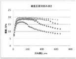
光透過性材料(及びこのような材料を含む物品)は、バーコビッチ圧子硬度試験によって測定される硬度に関して説明され得る。一つ以上の実施形態では、光透過性材料は、約100ナノメートル以上の凹み深さに沿ってバーコビッチ圧子硬度試験により400ナノメートル、500ナノメートル、1マイクロメートル、又は、2マイクロメートルの厚さを有する材料の主表面で測定されると、約12GPa以上の固有の最大硬度を示す。固有の最大硬度とは、材料が配置され得る、全ての下にある基板又は表面に関わりない材料自体の硬度である。 Light transmissive materials (and articles containing such materials) can be described in terms of hardness as measured by the Berkovich indenter hardness test. In one or more embodiments, the light transmissive material has a thickness of 400 nanometers, 500 nanometers, 1 micrometer, or 2 micrometers according to the Berkovich indenter hardness test along a recess depth of about 100 nanometers or more. When measured on the major surface of a material having a hardness, it exhibits an inherent maximum hardness of about 12 GPa or more. The inherent maximum hardness is the hardness of the material itself, regardless of the underlying substrate or surface on which the material can be placed.
本願で使用されるように、「バーコビッチ圧子硬度試験」は、ダイアモンドバーコビッチ圧子を用いて表面に凹みをつけることで、その表面上の材料の硬度を測定することを含む。バーコビッチ圧子硬度試験は、ダイアモンドバーコビッチ圧子を用いて材料の主表面又は物品のコーティング表面122(或いは、本願記載の全ての一層以上の層の表面)に凹みをつけて、特定される凹み深さまで凹みを形成し(或いは、試験される材料の全厚さ、いずれか小さい方)、Oliver,W.C.;Pharr,G.M.による「負荷及び変位感知凹み実験を用いて硬度及び弾性率を決定する改良された技術( An improved technique for determining hardness and elastic modulus using load and displacement sensing indentation experiments)」、J.Mater.Res.,Vol.7,No.6,1992年、1564−1583、及び、Oliver,W.C.;Pharr,G.M.による「機器の凹みによる硬度及び弾性率の測定:方法への理解及び改良の進歩(Measurement of Hardness and Elastic Modulus by Instrument Indentation: Advances in Understanding and Refinements to Methodology.)」、J.Mater.Res.,Vol.19,No.1,2004年、3−20記載の方法を用いて識別される凹み深さ範囲全体又は該凹み深さの識別されるセグメント(例えば、約100nm乃至600nmの範囲)に沿って該凹みから最大硬度を測定することを含む。本願で使用されるように、硬度は平均硬度ではなく最大硬度を意味する。従って、凹み深さの関数としての固有最大硬度又は最大硬度が図6に示される。図6では、各曲線は50nmより大きい、又は、100nmより大きい凹み深さに沿って12GPaの最大硬度を示す。硬度は凹み深さが深くなると低下するが、凹み範囲に沿って測定された最大硬度は12GPa以上、15GPa以上、又は、16GPa以上である。
As used herein, the "Verkovich indenter hardness test" involves measuring the hardness of the material on the surface by indenting the surface using a Diamond Burkovich indenter. The Berkovich Indenter Hardness Test is used to indent the major surface of the material or the
一つ以上の実施形態では、光透過性材料は、x線回折や透過型電子顕微鏡(TEM)によって測定されると略アモルファスな構造を有する。一つ以上の実施形態では、光透過性材料は、1マイクロメートルの厚さに沿ってTEM画像によって測定されると、非柱状形態を有する。 In one or more embodiments, the light transmissive material has a substantially amorphous structure as measured by x-ray diffraction or transmission electron microscopy (TEM). In one or more embodiments, the light transmissive material has a non-columnar morphology as measured by TEM imaging along a thickness of 1 micrometer.
一つ以上の実施形態では、光透過性材料は、約−1000MPa乃至100MPaの範囲の圧縮応力を有する。一つ以上の実施形態では、光透過性材料は、約−1000MPa乃至約100MPa、約−900MPa乃至約100MPa、約−800MPa乃至約100MPa、約−700MPa乃至約100MPa、約−600MPa乃至約100MPa、約−500MPa乃至約100MPa、約−400MPa乃至約100MPa、約−300MPa乃至約100MPa、約−200MPa乃至約100MPa、約−100MPa乃至約100MPa、又は、約−50MPa乃至約50MPaの範囲の圧縮応力を有する。光透過性材料の圧縮応力を決定するために、1マイクロメートルの厚さの材料の層が基板上に配置され、層が形成される前後に側面計を用いて下の基板の湾曲率が測定される。層は、真空蒸着技術を用いて形成される。光透過性材料が配置される基板は、約1mmの厚さと、5cm×5cmの寸法の長さと幅を有する。 In one or more embodiments, the light transmissive material has a compressive stress in the range of about -1000 MPa to 100 MPa. In one or more embodiments, the light transmissive material can be about -1000 MPa to about 100 MPa, about -900 MPa to about 100 MPa, about -800 MPa to about 100 MPa, about -700 MPa to about 100 MPa, about -600 MPa to about 100 MPa, about It has a compressive stress in the range of -500 MPa to about 100 MPa, about -400 MPa to about 100 MPa, about -300 MPa to about 100 MPa, about -200 MPa to about 100 MPa, about -100 MPa to about 100 MPa, or about -50 MPa to about 50 MPa. In order to determine the compressive stress of the light transmissive material, a layer of material of 1 micrometer thickness is placed on the substrate and the curvature of the lower substrate is measured using a side gauge before and after the layer is formed Be done. The layer is formed using a vacuum evaporation technique. The substrate on which the light transmissive material is disposed has a thickness of about 1 mm and a length and width of 5 cm × 5 cm.
一つ以上の実施形態では、光透過性材料は、550nmの波長で測定されると約2.0以上の屈折率を有する。幾つかの実施形態では、屈折率は、550nmの波長で測定されると約2.05以上、2.1以上、2.15以上、又は、2.2以上でもよい。 In one or more embodiments, the light transmissive material has a refractive index of about 2.0 or greater when measured at a wavelength of 550 nm. In some embodiments, the refractive index may be about 2.05 or more, 2.1 or more, 2.15 or more, or 2.2 or more as measured at a wavelength of 550 nm.
一つ以上の実施形態の光透過性材料は、1.5nm未満の固有の粗さ(Ra)を有する。固有の粗さは、真空蒸着技術を用いて0.4マイクロメートル以上の厚さの光透過性材料の層を形成し、次に2マイクロメートル×2マイクロメートルの寸法を有する撮像域に沿って原子間力顕微鏡(AFM)を用いて層の主表面の粗さを測定することで測定される。一つ以上の実施形態では、光透過性材料は、約1.2nm以下、1nm以下、又は、0.8nm以下の固有の粗さ(Ra)を有する。 The light transmissive material of one or more embodiments has an inherent roughness (Ra) of less than 1.5 nm. The inherent roughness forms a layer of light transmissive material of 0.4 micrometers or more in thickness using vacuum deposition techniques and then along the imaging area with dimensions of 2 micrometers by 2 micrometers It is measured by measuring the roughness of the main surface of the layer using an atomic force microscope (AFM). In one or more embodiments, the light transmissive material has an inherent roughness (Ra) of about 1.2 nm or less, 1 nm or less, or 0.8 nm or less.
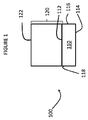
図1を参照するに、本開示の第二の様態は、基板110と基板上に配置される光学フィルム120とを含む物品100に関わる。基板110は、対向する主表面112、114及び対向する非主表面116、118を有する。光学フィルム120は、第一の対向する主表面112上に配置されるとして図1に示されるが、光学フィルム120は、第一の対向する主表面112に配置されることに加えて或いはその代わりに第二の対向する主表面114及び/又は対向する非主表面の片方または両方に配置されてもよい。光学フィルム120はコーティングされた表面122を形成する。
Referring to FIG. 1, a second aspect of the present disclosure relates to an
光学フィルム120の厚さは、本願記載の光学性能を示す物品を提供しつつ約400nm以上でもよい。幾つかの例では、光学フィルム120の厚さは、約400nm乃至約5μm(例えば、約400nm乃至約5μm、約500nm乃至約5μm、約600nm乃至約5μm、約800nm乃至約5μm、約1μm乃至約5μm、約1.2μm乃至約5μm、約1.4μm乃至約5μm、約1.5μm乃至約5μm、約1.6μm乃至約5μm、約1.8μm乃至約5μm、約2μm乃至約5μm)の範囲でもよい。
The thickness of the
光学フィルム120は、本願記載の光透過性材料の一つ以上の実施形態を含む。光透過性材料は、別個の層として光学フィルム120に存在してもよい。「層」といった用語は、単一の層でもよく、又は、一層以上のサブ層を含んでもよい。サブ層は、互いと直接的に接触していてもよい。そのようなサブ層は、同じ材料から形成されるか二種類以上の異なる材料から形成されてもよい。一つ以上の代替の実施形態では、そのようなサブ層の間に異なる材料の介在層が設けられてもよい。一つ以上の実施形態では、層は、一層以上の連続的で中断されない層及び/又は一層以上の非連続的で中断される層(すなわち、異なる材料の層が互いと隣接して形成される)を含んでもよい。層又はサブ層は、不連続的蒸着又は連続的蒸着処理を含む当技術分野で公知の任意の方法によって形成され得る。一つ以上の実施形態では、層は、連続的蒸着処理だけ、或いは、不連続的蒸着処理だけを用いて形成されてもよい。
本願で使用するように、「配置」といった用語は、当技術分野で公知の任意の方法を用いて表面上に材料をコーティング、堆積、及び/又は形成することを含む。配置された材料は、本願で定義するように、層を構成してもよい。「上に配置される」といった表現は、材料が表面と直接接触するよう表面上に材料を形成する例と、さらに、一つ以上の介在材料が、配置された材料と表面との間に設けられた状態で材料が表面上に形成される例も含む。介在材料は、本願で定義するように、層を構成してもよい。 As used herein, the term "arrangement" includes coating, depositing, and / or forming material on a surface using any method known in the art. The disposed material may constitute a layer as defined in the present application. The expression "disposed over" refers to the example of forming the material on the surface such that the material is in direct contact with the surface, and further, one or more intervening materials are provided between the material and the surface disposed. Also includes an example in which the material is formed on the surface in a fixed state. The intervening material may constitute a layer as defined in the present application.
一つ以上の実施形態では、光学フィルム120は、第二の層132を含んでもよい。一つ以上の実施形態では、第二の層は、第一の層と異なる材料を含んでもよい。第一の層130が基板の主表面112上に直接配置され(どの介在層も設けられない)、第二の層132が第一の層130上に配置されてもよい。一つ以上の実施形態では、第二の層132が基板の主表面112上に直接配置され(どの介在層も設けられない)、第一の層130が第二の層132上に配置されてもよい。
In one or more embodiments,
図2に示すように、光学フィルム120は、第一の層130と第二の層132とを交互に含む。一つ以上の実施形態では、第二の層は、第一の層とは異なる材料から形成されてもよい。幾つかの実施形態では、第二の層は、第一の層を形成する光透過性材料よりも小さい屈折率を有し得る。第二の層に使用する好適な材料の例として、SiO2、Al2O3、GeO2、SiO、AlOxNy、SiOxNy、SiuAlvOx、SiuAlvOxNy、MgO、MgAl2O4、MgF2、BaF2、CaF2、DyF3、YbF3、YF3、及び、CeF3が挙げられる。第二の層に使用する材料の窒素含有量は最小化してもよい(例えば、Al2O3及びMgAl2O4等の材料)。
As shown in FIG. 2, the
一つ以上の実施形態では、第一の層及び第二の層の少なくとも一方が特定の光学的厚さ範囲を有してもよい。本願で使用されるように、「光学的厚さ」は(n*d)によって決定され、「n」は層の屈折率、「d」は層の物理的厚さを示す。一つ以上の実施形態では、第一の層及び第二の層の少なくとも一方は約2nm乃至約200nm、約10nm乃至100nm、約15nm乃至約100nm、約15乃至約500nm、又は、約15乃至約5000nmの範囲の光学的厚さを有してもよい。幾つかの実施形態では、光学フィルム120における全ての層がそれぞれ約2nm乃至約200nm、約10nm乃至100nm、約15nm乃至約100nm、約15乃至約500nm、又は、約15乃至約5000nmの範囲の光学的厚さを有してもよい。ある場合では、光学フィルム120の少なくとも一層は約50nm以上の光学的厚さを有する。ある場合では、第一の層それぞれは、約2nm乃至約200nm、約10nm乃至100nm、約15nm乃至約100nm、約15乃至約500nm、又は、約15乃至約5000nmの範囲の光学的厚さを有する。他の場合では、第二の層それぞれは、約2nm乃至約200nm、約10nm乃至100nm、約15nm乃至約100nm、約15乃至約500nm、又は、約15乃至約5000nmの範囲の光学的厚さを有する。
In one or more embodiments, at least one of the first layer and the second layer may have a particular optical thickness range. As used herein, "optical thickness" is determined by (n * d), where "n" denotes the refractive index of the layer and "d" denotes the physical thickness of the layer. In one or more embodiments, at least one of the first layer and the second layer is about 2 nm to about 200 nm, about 10 nm to 100 nm, about 15 nm to about 100 nm, about 15 to about 500 nm, or about 15 to about It may have an optical thickness in the range of 5000 nm. In some embodiments, all layers in the
幾つかの実施形態では、光学フィルム120の一層以上の厚さが最小化されてもよい。一つ以上の実施形態では、第一の層の厚さは、約500nm未満となるよう最小化される。
In some embodiments, one or more thicknesses of
幾つかの実施形態では、体積による第二の層の厚さ又は量が最小化されてもよい。理論によって制限されることなく、第二の層が第一の層よりも屈折率が低い場合、第二の層も、屈折率及び硬度に同時に影響を与える原子結合及び電子密度の性質により、典型的には低硬度材料より形成され、それにより、該材料を最小化して本願記載の反射率及び色性能を維持しながら光学フィルム及び物品の硬度を最大化することができる。光学コーティングの物理的厚さの一部分として表わすと、第二の層は光学フィルムの物理的厚さの約60%未満、約50%未満、約40%未満、約30%未満、約20%未満、約10%未満、又は、約5%未満を有してもよい。 In some embodiments, the thickness or amount of the second layer by volume may be minimized. Without being limited by theory, when the second layer has a lower index of refraction than the first layer, the second layer is also typically represented by the nature of atomic bonding and electron density, which simultaneously affect the index of refraction and hardness. In particular, it is formed of a low hardness material, which can be minimized to maximize the hardness of the optical films and articles while maintaining the reflectance and color performance described herein. When expressed as a fraction of the physical thickness of the optical coating, the second layer is less than about 60%, less than about 50%, less than about 40%, less than about 30%, less than about 20% of the physical thickness of the optical film. , May be less than about 10%, or less than about 5%.
光学フィルム120及び物品100は、バーコビッチ圧子硬度試験によって測定される硬度について説明され得る。典型的には、下にある基板よりも硬いフィルムのナノ凹み測定方法(例えば、バーコビッチ圧子を用いて)では、測定された硬度は浅い凹み深さでプラスチックゾーンの発展により最初増加するように見られ、続いて、増加し、より深い凹み深さで最大値又は平坦域に達する。その後、硬度は、下にある基板の影響により、より深い凹み深さで低下し始める。フィルムと比べて増加した硬度を有する基板が利用される場合、同じ効果が得られるが、硬度は、下にある基板の影響によりより深い凹み深さで増加する。
凹み深さ範囲及びある凹み深さでの硬度値は、下にある基板に影響されることなく、本願に記載するように、光学フィルム構造及びその層の特定の硬度応答を識別するよう選択され得る。バーコビッチ圧子で光学フィルム構造(基板上に配置さえる場合)の硬度を測定する場合、材料の永久変形(プラスチックゾーン)の領域は、材料の硬度と関連付けられる。凹み中、弾性応力場は、永久変形の該領域をはるかに超えて延在する。凹み深さが増加すると、見掛け硬度及び係数は、下にある基板との応力場相互作用によって影響を及ぼされる。より深い凹み深さ(即ち、典型的には、光学フィルム構造又は層の厚さの約10%より大きい深さ)で、硬度への基板の影響が生じる。更に、更なる問題は、硬度応答が凹み処理中に完全な可塑性を展開するために一定の最小限の負荷を必要とする。一定の最小限の負荷の前に、硬度は、略増加する傾向を示す。 The indentation depth range and the hardness values at some indentation depths are selected to identify the specific hardness response of the optical film structure and its layers as described herein without being affected by the underlying substrate obtain. When measuring the hardness of an optical film structure (if placed on a substrate) with a Berkovich indenter, the area of permanent deformation (plastic zone) of the material is associated with the hardness of the material. During depression, the elastic stress field extends far beyond the area of permanent deformation. As the recess depth increases, the apparent hardness and modulus are affected by the stress field interaction with the underlying substrate. The deeper indentation depth (ie, typically greater than about 10% of the thickness of the optical film structure or layer) results in the effect of the substrate on hardness. Furthermore, a further problem is that the hardness response requires a certain minimum load to develop full plasticity during the indenting process. The hardness tends to increase substantially before a certain minimum load.
小さい凹み深さ(小さい負荷としても特徴付けられる)(例えば、約50nmまで)では、材料の見掛け硬度は、凹み深さに対して劇的に増加するように見える。この小さい凹み深さレジームは、硬度の真のメートル法を表さず、代わりに、圧子の有限湾曲率半径に関連する前述のプラスチックゾーンの展開を反映する。中間の凹み深さでは、見掛け硬度は最大レベルに近づく。より深い凹み深さでは、基板の影響は、凹み深さが増加するにつれてより顕著になる。硬度は、凹み深さが光学フィルム構造の厚さ又は層の厚さの約30%を一旦超えると劇的に低下する場合がある。 At small recess depths (also characterized as small loads) (eg, up to about 50 nm), the apparent hardness of the material appears to increase dramatically with recess depth. This small indentation depth regime does not represent a true metric of hardness, but instead reflects the development of the aforementioned plastic zone in relation to the finite radius of curvature of the indenter. At intermediate recess depths, the apparent hardness approaches the maximum level. At deeper indented depths, the effect of the substrate becomes more pronounced as the indented depth increases. The hardness may decrease dramatically once the recess depth exceeds about 30% of the thickness of the optical film structure or layer.
幾つかの実施形態では、光学フィルム120は、約8GPa以上、約10GPa以上、又は、約12GPa以上(例えば、14GPa以上、16GPa以上、18GPa以上、20GPa以上)の固有の最大硬度を示してもよい。光学フィルム120の固有の最大硬度は、約20GPa又は30GPaまででもよい。本願に記載するように、光学フィルム120及び全ての追加的なコーティングを含む物品100は、バーコビッチ圧子硬度試験によってコーティングされた表面122で測定されると、約5GPa以上、約8GPa以上、約10GPa以上、又は、約12GPa以上(例えば、14GPa以上、16GPa以上、18GPa以上、20GPa以上)の硬度を示す。このような測定された硬度値は、約50nm以上又は約100nm以上(例えば、約100nm乃至約300nm、約100nm乃至約400nm、約100nm乃至約500nm、約100nm乃至約600nm、約200nm乃至約300nm、約200nm乃至約400nm、約200nm乃至約500nm、又は、約200nm乃至約600nm)の凹み深さに沿って光学フィルム120及び/又は物品100によって示されてもよい。一つ以上の実施形態では、物品は基板の硬度(コーティングされた表面の反対表面で測定され得る)よりも大きい硬度を示す。上述の光学フィルムの固有の最大硬度と関連付けられる光学フィルムの厚さは、約200ナノメートル乃至約2マイクロメートルの範囲にあってもよい。
In some embodiments, the
一つ以上の実施形態では、光学フィルム120は、x線回折及び透過型電子顕微鏡(TEM)によって測定されると略アモルファスな構造を有する。一つ以上の実施形態では、光学フィルム120は、1マイクロメートルの厚さに沿ってTEM画像により測定されると、非柱状形態を有する。
In one or more embodiments,
一つ以上の実施形態では、物品の光学フィルム120は、約−1000MPa乃至100MPaの範囲の圧縮応力を有する。一つ以上の実施形態では、光学フィルムは、約−1000MPa乃至約100MPa、約−900MPa乃至約100MPa、約−800MPa乃至約100MPa、約−700MPa乃至約100MPa、約−600MPa乃至約100MPa、約−500MPa乃至約100MPa、約−400MPa乃至約100MPa、約−300MPa乃至約100MPa、約−200MPa乃至約100MPa、約−100MPa乃至約100MPa、又は、約−50MPa乃至約50MPaの範囲の圧縮応力を有する。光学フィルムの圧縮応力は、光透過性材料を参照して上述したのと同様に測定されるが、光学フィルムが形成される前後に物品の基板110の湾曲率半径が測定される。
In one or more embodiments, the
本開示の一つの様態は、発光体の下異なる入射照明角度で見た場合にでも反射率及び/又は透過率において無色を示す物品に関わる。一つ以上の実施形態では、物品は、本願記載の範囲における基準照明角度と全ての入射照明角度との間で約5以下又は約2以下の反射率及び/又は透過率における角度色ずれを示す。本願で使用するように、「色ずれ」(角度又は基準点)といった表現は、反射率及び/又は透過率におけるCIE L*、a*、b*測色システムの下、a*及びb*の両方における変化を意味する。ここで、特に記載しない限り、本願記載の物品のL*座標は全ての角度又は基準点において同じであり、色ずれに影響を与えないことは理解されるであろう。例えば、角度色ずれは、次の式を用いて決定されてもよい:
√((a* 2−a* 1)2+(b* 2−b* 1)2)
このとき、入射照明角度が基準照明角度と異なり、幾つかの場合では、少なくとも約1度、2度、又は、約5度だけ基準照明角度と異なるとして、a* 1及びb* 1は、入射基準照明角度(直角入射を含んでもよい)で見た場合に物品のa*及びb*座標を表し、a* 2及びb* 2は、入射基準照明角度で見た場合に物品のa*及びb*座標を表わす。幾つかの場合では、発光体の下、基準照明角度から様々な入射照明角度で見た場合に、物品によって約10以下(例えば、5以下、4以下、3以下、又は、2以下)の反射率及び/又は透過率における角度色ずれが示される。幾つかの場合では、反射率及び/又は透過率における角度色ずれは、約1.9以下、1.8以下、1.7以下、1.6以下、1.5以下、1.4以下、1.3以下、1.2以下、1.1以下、1以下、0.9以下、0.8以下、0.7以下、0.6以下、0.5以下、0.4以下、0.3以下、0.2以下、又は、0.1以下である。幾つかの実施形態では、角度色ずれは約0である。発光体は、A発光体(タングステンフィラメント照明)、B発光体(発光体をシミュレートする昼光)、C発光体(発光体をシミュレートする昼光)、Dシリーズ発光体(自然昼光を表す)、及び、Fシリーズ発光体(様々なタイプの蛍光照明を表す)を含み、CIEによって決定されるような標準発光体を含んでもよい。特定の実施例では、物品は、CIE F2、F10、F11、F12、又は、D65発光体の下、具体的には、CIE F2発光体の下で基準照明角度から入射照明角度で見た場合に約2以下の反射率及び/又は透過率における角度色ずれを示す。
One aspect of the present disclosure involves an article exhibiting achromaticity in reflectance and / or transmission even when viewed at different incident illumination angles below the light emitter. In one or more embodiments, the article exhibits an angular color shift in reflectance and / or transmission of about 5 or less or about 2 or less between the reference illumination angle and all incident illumination angles in the ranges described herein. . As used herein, the expression "color shift" (angle or reference point) refers to a * and b * under the CIE L * , a * , b * colorimetry system in reflectance and / or transmittance. It implies a change in both. Here, it will be understood that, unless otherwise stated, the L * coordinates of the article described herein are the same at all angles or reference points and do not affect color shift. For example, angular color shift may be determined using the following equation:
√ ((a * 2- a * 1 ) 2 + (b * 2- b * 1 ) 2 )
At this time, a * 1 and b * 1 are incident as the incident illumination angle is different from the reference illumination angle, and in some cases it differs from the reference illumination angle by at least about 1 degree, 2 degrees, or about 5 degrees, when viewed in the reference illumination angle (which may include normal incidence) to represent the a * and b * coordinates of the article, a * 2 and b * 2 is, a * and of the article when viewed by entering reference illumination angle b * represents coordinates. In some cases, a reflection of about 10 or less (e.g., 5 or less, 4 or less, 3 or less, or 2 or less) depending on the article when viewed under the light emitter at various incident illumination angles from a reference illumination angle An angular color shift in the rate and / or transmittance is indicated. In some cases, the angular color shift in reflectance and / or transmittance is about 1.9 or less, 1.8 or less, 1.7 or less, 1.6 or less, 1.5 or less, 1.4 or less, 1.3 or less, 1.2 or less, 1.1 or less, 1 or less, 0.9 or less, 0.8 or less, 0.6 or less, 0.6 or less, 0.5 or less, 0.4 or less, 0. It is 3 or less, 0.2 or less, or 0.1 or less. In some embodiments, the angular color shift is about zero. The luminous body includes A luminous body (tungsten filament illumination), B luminous body (daylight simulating luminous body), C luminous body (daylight simulating luminous body), D series luminous body (natural daylight) And F-series emitters (representing different types of fluorescent illumination) and may include standard emitters as determined by CIE. In particular embodiments, the article is viewed under the CIE F2, F10, F11, F12 or D65 emitters, specifically under the CIE F2 emitters, as viewed from the reference illumination angle at an incident illumination angle. 7 shows angular color shift at reflectance and / or transmittance of about 2 or less.
基準照明角度は、基準照明角度と入射照明角度と基準照明角度との間の差における差が、少なくとも約1度、2度、又は、5度であるとして、直角入射(即ち、約0度乃至約10度)、又は、直角入射から5度、直角入射から10度、直角入射から15度、直角入射から20度、直角入射から25度、直角入射から30度、直角入射から35度、直角入射から40度、直角入射から50度、直角入射から55度、又は、直角入射から60度を含んでもよい。入射照明角度は、基準照明角度に対して、約5度乃至約80度、約5度乃至約70度、約5度乃至約65度、約5度乃至約60度、約5度乃至約55度、約5度乃至約50度、約5度乃至約45度、約5度乃至約40度、約5度乃至約35度、約5度乃至約30度、約5度乃至約25度、約5度乃至約20度、約5度乃至約15度の範囲、及び、その間の全ての範囲及びサブ範囲だけ基準照明角度から離れていてもよい。物品は、基準照明角度が直角入射の場合、約2度乃至約80度(又は、約10度乃至約80度、又は、約20度乃至約80度)の範囲の全ての入射照明角度においてかつそれに沿って、本願に記載する反射率及び/又は透過率における角度色ずれを示してもよい。幾つかの実施形態では、物品は、入射照明角度と基準照明角度との間の差が少なくとも約1度、2度、又は、約5度の場合に、約2度乃至約80度(又は、約10度乃至約80度、又は、約20度乃至約80度)の範囲の全ての入射照明角度においてかつそれに沿って、本願に記載する反射率及び/又は透過率における角度色ずれを示してもよい。一例では、物品は、直角入射に等しい基準照明角度から約2度乃至役60度、約5度乃至約60度、又は、約10度乃至約60離れた範囲における全ての入射照明角度において5以下(例えば、4以下、3以下、又は、約2以下)の反射率及び/又は透過率における角度色ずれを示してもよい。他の例では、物品は、基準照明角度が10度であり、入射照明角度が基準照明角度から約12度乃至役60度、約15度乃至約60度、又は、約20度乃至約60離れた範囲における全ての角度の場合に、5以下(例えば、4以下、3以下、又は、約2以下)の反射率及び/又は透過率における角度色ずれを示してもよい。 The reference illumination angle is normal incidence (i.e., about 0 degrees to about 0 degrees), with the difference in the difference between the reference illumination angle and the incident illumination angle and the reference illumination angle being at least about 1 degree, 2 degrees, or 5 degrees. 10 degrees) or 5 degrees from normal incidence, 10 degrees from normal incidence, 15 degrees from normal incidence, 20 degrees from normal incidence, 25 degrees from normal incidence, 30 degrees from normal incidence, 35 degrees from normal incidence It may include 40 degrees from incidence, 50 degrees from normal incidence, 55 degrees from normal incidence, or 60 degrees from normal incidence. The incident illumination angle is about 5 degrees to about 80 degrees, about 5 degrees to about 70 degrees, about 5 degrees to about 65 degrees, about 5 degrees to about 60 degrees, about 5 degrees to about 55 degrees with respect to the reference illumination angle. Degrees, about 5 degrees to about 50 degrees, about 5 degrees to about 45 degrees, about 5 degrees to about 40 degrees, about 5 degrees to about 35 degrees, about 5 degrees to about 30 degrees, about 5 degrees to about 25 degrees, A range of about 5 degrees to about 20 degrees, about 5 degrees to about 15 degrees, and all ranges and subranges therebetween may be separated from the reference illumination angle. The article is for all incident illumination angles in the range of about 2 degrees to about 80 degrees (or about 10 degrees to about 80 degrees, or about 20 degrees to about 80 degrees) when the reference illumination angle is normal incidence and Along with that, the angular color shift in reflectance and / or transmittance described herein may be indicated. In some embodiments, the article is about 2 degrees to about 80 degrees (or, when the difference between the incident illumination angle and the reference illumination angle is at least about 1 degree, 2 degrees, or about 5 degrees. At and along all incident illumination angles ranging from about 10 degrees to about 80 degrees, or about 20 degrees to about 80 degrees), to indicate the angular color shift in reflectance and / or transmission described herein It is also good. In one example, the article has five or less at all incident illumination angles in the range of about 2 degrees to about 60 degrees, about 5 degrees to about 60 degrees, or about 10 degrees to about 60 degrees from a reference illumination angle equal to normal incidence. An angular color shift in reflectance and / or transmittance (e.g., 4 or less, 3 or less, or about 2 or less) may be indicated. In other examples, the article has a reference illumination angle of 10 degrees and an incident illumination angle of about 12 degrees to about 60 degrees from the reference illumination angle, about 15 degrees to about 60 degrees, or about 20 degrees to about 60 degrees away For all angles in the range, an angular color shift in reflectance and / or transmittance of 5 or less (e.g., 4 or less, 3 or less, or about 2 or less) may be exhibited.
幾つかの実施形態では、角度色ずれは、約20度乃至約80度の範囲において基準照明角度(例えば、直角入射)と入射照明角度との間の全ての角度において測定されてもよい。つまり、角度色ずれは測定されてもよく、約0度乃至20度、約0度乃至約30度、約0度乃至約40度、約0度乃至約50度、約0度乃至約60度、又は、約0度乃至約80度の範囲の全ての角度において約5未満又は約2未満でもよい。 In some embodiments, the angular color shift may be measured at all angles between the reference illumination angle (e.g., normal incidence) and the incident illumination angle in the range of about 20 degrees to about 80 degrees. That is, angular color shift may be measured: about 0 degrees to 20 degrees, about 0 degrees to about 30 degrees, about 0 degrees to about 40 degrees, about 0 degrees to about 50 degrees, about 0 degrees to about 60 degrees Or, it may be less than about 5 or less than about 2 at all angles ranging from about 0 degrees to about 80 degrees.
一つ以上の実施形態では、物品は、発光体(A発光体(タングステンフィラメント照明)、B発光体(発光体をシミュレートする昼光)、C発光体(発光体をシミュレートする昼光)、Dシリーズ発光体(自然昼光を表す)、及び、Fシリーズ発光体(様々なタイプの蛍光照明を表す)を含み、CIEによって決定されるような標準発光体を含んでもよい)の下、基準点から透過色又は反射色座標間の距離又は基準点の色ずれが約5以下又は約2以下となるよう反射率及び/又は透過率においてCIE L*、a*、b*測色システムにおいて色を示す。特定の実施例では、物品は、CIE F2、F10、F11、F12、又は、D65発光体の下、具体的には、CIE F2発光体の下で基準照明角度から入射照明角度で見た場合に約2以下の反射率及び/又は透過率における色ずれを示す。別の言い方をすると、物品は、本願で定義するように、基準点から約2未満の基準点の色ずれを有するコーティングされた表面122で測定される透過色(又は、透過色座標)及び/又は反射色(又は反射色座標)を示してもよい。特に記載しない限り、透過色又は透過色座標は、物品のコーティングされた表面122及び反対側の素表面(即ち、114)を含む物品の二つの表面で測定される。特に記載しない限り、反射色又は反射色座標は、物品のコーティングされた表面122のみで測定される。しかしながら、本願記載の反射色又は反射色座標は、2−表面測定(物品の両側からの反射がそれぞれ含まれる)又は1−表面測定(物品のコーティングされた表面122からの反射だけが測定される)を用いて、物品のコーティングされた表面122及び物品の反対側(即ち、図1において主表面114)の両方で測定され得る。
In one or more embodiments, the article comprises a light emitter (A light emitter (tungsten filament illumination), a B light emitter (daylight simulating a light emitter), a C light emitter (daylight simulating a light emitter) , D-series emitters (representing natural daylight) and F-series emitters (including various types of fluorescent illumination, and may include standard emitters as determined by CIE), In the CIE L * , a * , b * colorimetric system in reflectance and / or transmittance so that the distance between the reference point to the transmitted color or reflected color coordinates or the color deviation of the reference point is about 5 or less or about 2 or less Show the color. In particular embodiments, the article is viewed under the CIE F2, F10, F11, F12 or D65 emitters, specifically under the CIE F2 emitters, as viewed from the reference illumination angle at an incident illumination angle. 7 shows a color shift at a reflectance and / or transmittance of about 2 or less. Stated differently, the article may have a transmitted color (or transmitted color coordinates) and / or measured on the
一つ以上の実施形態では、基準点は、CIE L*、a*、b*測色システム(又は、色座標a*=0,b*=0)における原点(0,0)、座標(a*=−2,b*=−2)、又は、基板の透過又は反射色座標でもよい。特に記載しない限り、本願記載の物品のL*座標が基準点と同じであり、色ずれに影響を与えないことは理解されるであろう。基板に対して物品の基準点の色ずれが定義される場合、物品の透過色座標は基板の透過色座標と比較され、物品の反射色座標は基板の反射色座標と比較される。 In one or more embodiments, the reference point is the origin (0,0), coordinates (a) in the CIE L * , a * , b * colorimetric system (or color coordinates a * = 0, b * = 0). * = -2, b * =-2), or the transmitted or reflected color coordinates of the substrate. It will be appreciated that, unless otherwise stated, the L * coordinates of the article described herein are the same as the reference point and do not affect color shift. If a color shift of the reference point of the article relative to the substrate is defined, the transmitted color coordinates of the article are compared to the transmitted color coordinates of the substrate and the reflected color coordinates of the article are compared to the reflected color coordinates of the substrate.
一つ以上の具体的な実施形態では、透過色及び/又は反射色の基準点色ずれは1未満、又は、0.5未満であってもよい。一つ以上の具体的な実施形態では、透過色及び/又は反射色に対する基準点の色ずれは、1.8、1.6、1.4、1.2、0.8、0.6、0.4、0.2、0及びその間の全ての範囲及びサブ範囲でもよい。基準点が色座標a*=0,b*=0の場合、基準点の色ずれは、基準点の色ずれ=√ ((a* article)2 + (b* article)2)の式によって計算される。 In one or more specific embodiments, the reference point color shift of the transmitted and / or reflected colors may be less than 1 or less than 0.5. In one or more specific embodiments, the color shift of the reference point relative to the transmitted and / or reflected color is 1.8, 1.6, 1.4, 1.2, 0.8, 0.6, It may be 0.4, 0.2, 0 and all ranges and sub-ranges therebetween. When the reference point has color coordinates a * = 0 and b * = 0, the color shift of the reference point is calculated by the formula of color shift of the reference point = √ ((a * article ) 2 + (b * article ) 2 ) Be done.
基準点が色座標a*=−2,b*=−2の場合、基準点の色ずれは、基準点の色ずれ=√((a* article +2)2 + (b* article +2)2)の式によって計算される。 When the reference point has color coordinates a * = -2, b * = -2, the color shift of the reference point is the color shift of the reference point = (((a * article +2) 2 + (b * article +2) Calculated by the equation 2 ).
基準点が基板の色座標の場合、基準点の色ずれは、基準点の色ずれ=√((a* article−a* 基板)2 + (b* article−b* 基板)2)の式によって計算される。 When the reference point is the color coordinates of the substrate, the color shift of the reference point, by the equation of the reference point color deviation = √ ((a * article -a * substrate) 2 + (b * article -b * substrate) 2) Calculated
幾つかの実施形態では、物品は、基準点が基板の色座標、色座標a*=0、b*=0、及び、色座標a*=−2、b*=−2のいずれか一つである場合に基準点の色ずれが2未満であるように透過色(又は透過色座標)及び反射色(又は反射色座標)を示す。 In some embodiments, the article has a reference point that is any one of substrate color coordinates, color coordinates a * = 0, b * = 0, and color coordinates a * = − 2, b * = − 2 In this case, it indicates the transmission color (or transmission color coordinates) and the reflection color (or reflection color coordinates) such that the color shift of the reference point is less than 2.
一つ以上の実施形態では、物品は、約0乃至約60度(又は約0度乃至約40度或いは約0度乃至約30度)の範囲における全ての入射照明角度でのCIE L*、a*、b*測色システムにおいて約―5乃至約1、約―5乃至約0、約―4乃至約1、又は、約―4乃至約0の範囲の反射率(コーティングされた表面のみで測定される)におけるb*値を示してもよい。 In one or more embodiments, the article may have a CIE L * , a at all incident illumination angles in the range of about 0 to about 60 degrees (or about 0 degrees to about 40 degrees or about 0 degrees to about 30 degrees). * Reflectivity in the range of about -5 to about 1, about -5 to about 0, about -4 to about 1, or about -4 to about 0 in the * , b * colorimetric system (measured with coated surface only it may indicate a b * value in to).
一つ以上の実施形態では、物品は、約0乃至約60度(又は約0度乃至約40度或いは約0度乃至約30度)の範囲における全ての入射照明角度でのCIE L*、a*、b*測色システムにおいて約2未満(又は約1.8以下、約1.6以下、1.5以下、1.4以下、1.2以下、又は、約1以下)の透過率(物品のコーティングされた表面及び反対側の素表面で測定される)におけるb*値を示してもよい。透過率におけるb*値の下限は約―5でもよい。 In one or more embodiments, the article may have a CIE L * , a at all incident illumination angles in the range of about 0 to about 60 degrees (or about 0 degrees to about 40 degrees or about 0 degrees to about 30 degrees). * , B * Transmittance of less than about 2 (or about 1.8 or less, about 1.6 or less, 1.5 or less, 1.4 or less, 1.2 or less, or about 1 or less) in the colorimetric system The b * value may be shown at the coated surface of the article and at the opposite bare surface). The lower limit of the b * value in transmittance may be about -5.
幾つかの実施形態では、物品は、発光体D65、A、及び、F2の下で約0度乃至約60度の範囲における入射照明角度で約−1.5乃至約1.5(例えば、−1.5乃至―1.2、−1.5乃至―1、−1.2乃至1.2、−1乃至1、−1乃至0.5、又は、−1乃至0)の範囲の透過率(コーティングされた表面及び反対側の素表面における)におけるa*値を示す。幾つかの実施形態では、物品は、発光体D65、A、及び、F2の下で約0度乃至約60度の範囲における入射照明角度で約−1.5乃至約1.5(例えば、−1.5乃至―1.2、−1.5乃至―1、−1.2乃至1.2、−1乃至1、−1乃至0.5、又は、−1乃至0)の範囲の透過率(コーティングされた表面及び反対側の素表面における)におけるb*値を示す。 In some embodiments, the article comprises about -1.5 to about 1.5 (e.g.-) at an incident illumination angle ranging from about 0 degrees to about 60 degrees below the light emitters D65, A, and F2. Transmittance in the range of 1.5 to 1.2, -1.5 to -1, -1.2 to 1.2, -1 to 1, -1 to 0.5, or -1 to 0) The a * values at (on the coated surface and on the opposite bare surface) are shown. In some embodiments, the article comprises about -1.5 to about 1.5 (e.g.-) at an incident illumination angle ranging from about 0 degrees to about 60 degrees below the light emitters D65, A, and F2. Transmittance in the range of 1.5 to 1.2, -1.5 to -1, -1.2 to 1.2, -1 to 1, -1 to 0.5, or -1 to 0) The b * values at (on the coated surface and on the opposite bare surface) are shown.
幾つかの実施形態では、物品は、発光体D65、A、及び、F2の下で約5度乃至約60度の範囲における入射照明角度で約−5乃至約2(例えば、−4.5乃至1.5、−3乃至0、−2.5乃至0.25)の範囲の反射率(コーティングされた表面のみ)におけるa*値を示す。幾つかの実施形態では、物品は、発光体D65、A、及び、F2の下で約5度乃至約60度の範囲における入射照明角度で約−7乃至約0の範囲の反射率(コーティングされた表面のみ)におけるb*値を示す。 In some embodiments, the article comprises about -5 to about 2 (e.g. -4.5 to about 2 at an incident illumination angle in the range of about 5 degrees to about 60 degrees below the light emitters D65, A, and F2). The a * value at a reflectance (coated surface only) in the range of 1.5, -3 to 0, -2.5 to 0.25) is shown. In some embodiments, the article has a reflectance (coated) in the range of about -7 to about 0 at incident illumination angles in the range of about 5 degrees to about 60 degrees below the light emitters D65, A, and F2. shows the b * value at the surface only) was.
一つ以上の実施形態の物品は、光波長レジームについて約80%以上の平均透過率を示してもよい。一つ以上の実施形態では、物品は、全ての光波長レジームについて約82%以上、約84%以上、約86%以上、約88%以上、約90%以上、約92%以上、約94%以上、約95%以上、又は約96%以上、の平均透過率を示す。 The article of one or more embodiments may exhibit an average transmission of about 80% or more for the light wavelength regime. In one or more embodiments, the article is about 82% or more, about 84% or more, about 86% or more, about 88% or more, about 90% or more, about 92% or more, about 94% or more for all light wavelength regimes. Above, the average transmittance of about 95% or more, or about 96% or more is exhibited.
一つ以上の実施形態では、物品は低平均反射率を示す。例えば、物品は光波長レジームについて約15%以下(例えば、約20%以下、約18%以下、約16%以下、約15%以下、約14%以下、約12%以下、約10%以下、約8%以下、約6%以下、約5%以下、約4%以下、約3%以下、約2%以下、約1%以下、又は約0.5%以下)の平均反射率を示してもよい。 In one or more embodiments, the article exhibits a low average reflectance. For example, the article may have a light wavelength regime of about 15% or less (eg, about 20% or less, about 18% or less, about 16% or less, about 15% or less, about 14% or less, about 12% or less, about 10% or less Showing an average reflectance of about 8% or less, about 6% or less, about 5% or less, about 4% or less, about 3% or less, about 2% or less, about 1% or less, or about 0.5% or less) It is also good.
幾つかの実施形態では、これらの平均反射率及び平均透過率の値は、合計反射率又は合計透過率(コーティングされた表面122及び反対側の主表面114の両方における反射率又は透過率を考慮して)でもよい。幾つかの実施形態では、物品の報告された平均反射率は、コーティングされた表面122だけで測定されると(反対側の表面を考慮せず)、物品の平均片側反射率でもよい。特に記載しない限り、平均反射率は、垂直から5度の入射照明角度で測定され、平均透過率は直角入射で測定される。
In some embodiments, these average reflectance and average transmission values take into account the total reflectance or total transmission (reflectance or transmission on both the
基板
基板110は、無機材料を含んでもよく、アモルファス基板、結晶基板、又は、その組み合わせを含んでもよい。基板110は、人工材料及び/又は自然発生材料(例えば、クォーツ又はポリマー)より形成されてもよい。例えば、幾つかの場合では、基板110は有機的として特徴付けられ、具体的には高分子でもよい。好適なポリマーの例として、ポリスチレン(PS)(スチレンコポリマーや混合物を含む)、ポリカーボネート(PC)(コポリマーや混合物を含む)、ポリエステル(ポリエチレンテレフタレートやポリエチレンテレフタレートコポリマーを含むコポリマーや混合物を含む)、ポリオレフィン(PO)及び環状ポリオレフィン(環状PO)、ポリ塩化ビニル(PVC)、ポリメチルメタクリレート(PMMA)(コポリマー及び混合物を含む)を含むアクリルポリマー、熱可塑性ウレタン(TPU)、ポリエチルイミド(PEI),及び、これらポリマーの混合物を含む熱可塑性物質を含むがこれらに制限されない。他の例示的なポリマーはエポキシ、スチレン、フェノール、メラミン、及び、シリコーン樹脂を含む。
Substrate The
幾つかの特定の実施形態では、基板110はポリマー、プラスチック及び/又は金属基板を特定的に除外してもよい。基板は、アルカリ含有基板(即ち、一つ以上のアルカリを含む基板)として特徴付けられてもよい。一つ以上の実施形態では、基板は、約1.45乃至約1.55の範囲の屈折率を示す。具体的な実施形態では、基板110は、少なくとも5、少なくとも10、少なくとも15、又は、少なくとも20個のサンプルを用いたボールオンリング試験で測定されると約0.5%以上、0.6%以上、0.7%以上、0.8%以上、0.9%以上、1%以上、1.1%以上、1.2%以上、1.3%以上、1.4%以上、1.5%以上、又は、2%以上の一つ以上の対向する主表面における表面での平均破損応力を示してもよい。特定の実施形態では、基板110は、約1.2%、約1.4%、約1.6%、約1.8%、約2.2%、約2.4%、約2.6%、約2.8%、又は約3%以上の一つ以上の対向する主表面における表面での平均破損応力を示してもよい。
In some specific embodiments,
好適な基板110は、約30GPa乃至約120GPaの範囲の弾性率(又はヤング率)を示してもよい。幾つかの場合では、基板の弾性率は、約30GPa乃至約110GPa、約30GPa乃至約100GPa、約30GPa乃至約90GPa、約30GPa乃至約約80GPa、約30GPa乃至約70GPa、約40GPa乃至約120GPa、約50GPa乃至約120GPa、約60GPa乃至約120GPa、約70GPa乃至約120GPa、及び、間の全ての範囲及びサブ範囲の範囲でもよい。
A
一つ以上の実施形態では、アモルファス基板は、強化された、又は強化されていないガラスを含み得る。好適なガラスの例として、ソーダ石灰ガラス、アルカリアルミノシリケートガラス、アルカリ含有ボロシリケートガラス、及び、アルカリアルミノボロシリケートガラスが挙げられる。幾つかの変形例では、ガラスは酸化リチウムを含まない。一つ以上の代替の実施形態では、基板110はガラスセラミック基板(又は強化されていても、又は強化されていなくてもよい)等の結晶基板を含んでもよく、又は、サファイアのような単一結晶構造を含んでもよい。一つ以上の特定の実施形態では、基板110はアモルファスベース(例えば、ガラス)及び結晶クラッディング(例えば、サファイア層、多結晶アルミナ層及び/又はスピネル(MgAl2O4)層)を含む。
In one or more embodiments, the amorphous substrate can comprise a tempered or non-tempered glass. Examples of suitable glasses include soda lime glass, alkali aluminosilicate glass, alkali containing borosilicate glass, and alkali aluminoborosilicate glass. In some variations, the glass does not contain lithium oxide. In one or more alternative embodiments,
一つ以上の実施形態の基板110は、(本願記載のバーコビッチ圧子硬度試験によって測定される)物品の硬度よりも小さい硬度を有してもよい。基板の硬度は、バーコビッチ圧子硬度試験又はビッカーズ硬度試験を含むがこれに制限されない当技術分野で公知の方法を用いて測定されてもよい。
The
基板110は、略平面でもシート状でもよいが、他の実施形態は湾曲された或いはさもなければ成形された又は彫刻された基板を利用してもよい。基板110は、光学的にクリアで透明で光拡散がない。このような実施形態では、基板は、約85%以上、約86%以上、約87%以上、約88%以上、約89%以上、約90%以上、約91%以上、又は約92%以上の光波長レジームについての平均光透過率を示してもよい。一つ以上の代替の実施形態では、基板110は不透明か約10%未満、約9%未満、約8%未満、約7%未満、約6%未満、約5%未満、約4%未満、約3%未満、約2%未満、約1%未満、又は約0%未満の光波長レジームについての平均光透過率を示してもよい。幾つかの実施形態では、これら光反射率及び透過率の値は、合計反射率又は合計透過率(基板の両主表面における反射率又は透過率を考慮して)でもよく、または基板の片側で観察されてもよい(即ち、反対側の表面を考慮することなく反射防止表面122においてのみ)。特に特定しない限り、平均反射率又は透過率は、0度の入射照明角度で測定される(しかしながら、このような測定は、45度又は60度の入射照明角度で提供されてもよい)。基板110は、白、黒、赤、青、緑、黄、オレンジ等の色を任意に示してもよい。
The
追加的には、又は、代替的には、基板110の物理的な厚さは、美観的及び/又は機能的理由のためその一つ以上の寸法に沿って変化してもよい。例えば、基板110のエッジは基板110のより中央領域と比べて厚くてもよい。基板110の長さ、幅、及び、物理的厚さ寸法は、物品100の用途又は使用に応じて変化してもよい。
Additionally or alternatively, the physical thickness of
基板110は様々な異なる処理を用いて提供されてもよい。例えば、基板110がガラス等のアモルファス基板を含む場合、様々な形成方法はフロートガラス処理、フュージョンドローやスロットドロー等のダウンドロー処理を含み得る。
一旦形成されると、基板110は強化されて、強化基板が形成されてもよい。本願で使用するように、「強化基板」といった用語は、例えば、基板の表面における小さいイオンとの大きいイオンのイオン交換を通じて化学的に強化された基板を意味する。しかしながら、当技術分野で公知の他の強化方法、例えば、熱焼き戻し又は基板の部分間の熱膨張係数の不一致を利用して圧縮応力及び中央張力領域を形成することを利用して強化基板を形成してもよい。
Once formed, the
強化度は、中央張力(CT)、表面圧縮応力(CS)、及び、圧縮の深さ(DOC)のパラメータに基づいて定量化され得る。強化基板は、具体的には、第一の主表面112及び第二の主表面114の一方又は両方からDOCまで延在するCS層(表面CS値を有する)を含む。CT層又は領域は、DOCから基板の中央部分まで延在する。本願で使用するように、DOCは、基板内の応力が圧縮から引張に変化する深さを意味する。DOCにおいて、応力は正(圧縮)の応力から負(引張)の応力となり、したがってゼロの応力値を示す。
The degree of reinforcement can be quantified based on the parameters of central tension (CT), surface compressive stress (CS), and depth of compression (DOC). The reinforced substrate specifically comprises a CS layer (with a surface CS value) extending from one or both of the first
しかしながら、本説明を通じて、基板に対するCSは正又は絶対値、即ち、本願で記載するようにCS=|CS|として表される。 However, throughout this description, CS relative to the substrate is expressed as a positive or absolute value, ie, CS = | CS | as described herein.
圧縮応力(表面CSを含む)は、折原製作所(日本)によって製造されるFSM−6000等の市販の機器を用いた表面応力計(FSM)によって測定される。表面応力測定は、ガラスの複屈折に関連する応力光係数(SOC)の正確な測定に依存する。SOCもまた、「ガラス応力光係数の測定に対する標準試験方法」なる名称のASTM規格C770−16に記載される手順C(ガラスディスク方法)に応じて測定され、その内容は全体的が参照により本願に組み込まれる。 The compressive stress (including the surface CS) is measured by a surface stress meter (FSM) using a commercially available instrument such as FSM-6000 manufactured by Orihara Seisakusho (Japan). Surface stress measurement relies on accurate measurement of the stress light coefficient (SOC) associated with glass birefringence. The SOC is also measured according to Procedure C (Glass Disc Method) described in ASTM Standard C 770-16 entitled "Standard Test Method for Measurement of Glass Stress Light Coefficient", the contents of which are incorporated by reference in their entirety. Incorporated into
DOC及びCT値は、当技術分野で公知の散乱光偏光器(SCALP)を用いて測定される。 DOC and CT values are measured using a scattered light polarizer (SCALP) as known in the art.
一実施形態では、強化基板110は、250MPa以上、300MPa以上、例えば、400MPa以上、450MPa以上、500MPa以上、550MPa以上、600MPa以上、650MPa以上、700MPa以上、750MPa以上、又は800MPa以上の表面CSを有してもよい。強化基板は、10μm以上、15μm以上、20μm以上(例えば、25μm、30μm、35μm、40μm、45μm、50μm以上)のDOC及び/又は10MPa以上、20MPa以上、30MPa以上、40MPa以上、(例えば、42MPa、45MPa、又は、50MPa以上)で100MPa未満(例えば、95、90、85、80、75、70、65、60、55MPa以下)のCTを有してもよい。一つ以上の特定の実施形態では、強化基板は、500MPaより大きい表面CS、15μmより大きいDOC、及び、18MPaより大きいCTの一つ以上を有する。
In one embodiment, the reinforced
基板で使用され得る例示的なガラスは、アルカリアルミノシリケートガラス組成物又はアルカリアルミノボロシリケートガラス組成物を含んでもよいが他のガラス組成物も考えられ得る。このようなガラス組成物はイオン交換処理によって化学的に強化され得る。一つの例示的なガラス組成物は、SiO2、B2O3及びNa2Oを有し、このとき(SiO2+B2O3)≧66モル%及びNa2O≧9モル%である。一実施形態では、ガラス組成物は、少なくとも6重量%の酸化アルミニウムを含む。更なる実施形態では、基板は、一つ以上のアルカリ土類酸化物を有するガラス組成物を含み、例えば、アルカリ土類酸化物の含有量は少なくとも5重量%である。幾つかの実施形態では、好適なガラス組成物は、K2O、MgO及びCaOの少なくとも一つを更に有する。特定の実施形態では、基板において使用されるガラス組成物は、61乃至75モル%のSiO2、7乃至15モル%のAl2O3、0乃至12モル%のB2O3、9乃至21モル%のNa2O、0乃至4モル%のK2O、0乃至7モル%のMgO、及び、0乃至3モル%のCaOを有してもよい。 Exemplary glasses that may be used in the substrate may include alkaline aluminosilicate glass compositions or alkaline aluminoborosilicate glass compositions, but other glass compositions may also be considered. Such glass compositions can be chemically strengthened by ion exchange treatment. One exemplary glass composition comprises SiO 2, B 2 O 3 and Na 2 O, where (SiO 2 + B 2 O 3 ) ≧ 66 mole% and Na 2 O ≧ 9 mole%. In one embodiment, the glass composition comprises at least 6% by weight of aluminum oxide. In a further embodiment, the substrate comprises a glass composition having one or more alkaline earth oxides, for example, the content of alkaline earth oxides is at least 5% by weight. In some embodiments, suitable glass compositions further comprise at least one of K 2 O, MgO and CaO. In certain embodiments, the glass composition used in the substrate is 61 to 75 mol% of SiO2,7 to 15 mol% of Al 2 O 3, 0 to 12 mol% of B 2 O 3, 9 to 21 mol % Na 2 O, 0 to 4 mole% K 2 O, 0 to 7 mole% MgO, and 0 to 3 mole% CaO.
基板に好適な更なる例示的なガラス組成物は、60乃至70モル%のSiO2、6乃至14モル%のAl2O3、0乃至15モル%のB2O3、0乃至15モル%のLi2O、0乃至20モル%のNa2O、0乃至10モル%のK2O、0乃至8モル%のMgO、0乃至10モル%のCaO、0乃至5モル%のZrO2、0乃至1モル%のSnO2、0乃至1モル%のCeO2、50ppm未満のAs2O3、及び、50ppm未満のSb2O3を有し、このとき12モル%≦(Li2O+Na2O+K2O)≦20モル%及び0モル%≦(MgO+CaO)≦10モル%である。
Further exemplary glass compositions suitable for the substrate are 60 to 70 mole% SiO 2, 6 to 14 mole% Al 2 O 3, 0 to 15 mole% B 2 O 3, 0 to 15 mole% Li 2 O 2 , 0 to 20 mol% Na 2 O , 0 to 10 mol% K 2 O , 0 to 8
基板に好適な更なる例示的なガラス組成物は。63.5乃至66.5モル%のSiO2、8乃至12モル%のAl2O3、0乃至3モル%のB2O3、0乃至5モル%のLi2O、8乃至18モル%のNa2O、0乃至5モル%のK2O、1乃至7モル%のMgO、0乃至2.5モル%のCaO、0乃至3モル%のZrO2、0.05乃至0.25モル%のSnO2、0.05乃至0.5モル%のCeO2、50ppm未満のAs2O3及び50ppm未満のSb2O3を有し、このとき14モル%≦(Li2O+Na2O+K2O)≦18モル%及び2モル%≦(MgO+CaO)≦7モル%である。
Further exemplary glass compositions suitable for substrates. 63.5 to 66.5 mol% of
特定の実施形態では、基板に好適なアルカリアルミノシリケートガラス組成物は、アルミナ、少なくとも一つのアルカリ金属を含み、幾つかの実施形態では、50モル%を超えるSiO2、他の実施形態では少なくとも58モル%のSiO2、更に、他の実施形態では、少なくとも60モル%のSiO2を含み、このとき比(Al2O3+B2O3)/Σ変性剤(即ち、変性剤の合計)は1よりも大きく、該比では、成分はモル%で表され変性剤はアルカリ金属酸化物である。特定の実施形態におけるガラス組成物は、58乃至72モル%のSiO2、9乃至17モル%のAl2O3、2乃至12モル%のB2O3、8乃至16モル%のNa2O、及び、0乃至4モル%のK2Oを有し、このとき比(Al2O3+B2O3)/Σ変性剤(即ち、変性剤の合計)は1よりも大きい。
In certain embodiments, suitable alkali aluminosilicate glass composition to a substrate, alumina comprises at least one alkali metal, in some embodiments, at least a SiO 2, another embodiment of greater than 50 mole% 58 Mole% SiO 2 , and in another embodiment at least 60 mole% SiO 2 , wherein the ratio (Al 2 O 3 + B 2 O 3 ) / Σ modifier (ie, the sum of modifiers) is In the ratio, the component is expressed in mol% and the modifier is an alkali metal oxide. The glass composition in a specific embodiment comprises 58 to 72
更なる別の実施形態では、基板は、64乃至68モル%のSiO2、12乃至16モル%のNa2O、8乃至12モル%のAl2O3、0乃至3モル%のB2O3、2乃至5モル%のK2O、4乃至6モル%のMgO、及び、0乃至5モル%のCaOを含むアルカリアルミノシリケートガラス組成物を含んでもよく、このとき66モル%≦SiO2+B2O3+CaO≦69モル%、Na2O+K2O+B2O3+MgO+CaO+SrO>10モル%、5モル%≦MgO+CaO+SrO≦8モル%、(Na2O+B2O3)−Al2O3≦2モル%、2モル%≦Na2O−Al2O3≦6モル%、及び4モル%≦(Na2O+K2O)−Al2O3≦10モル%である。 In yet another embodiment, the substrate comprises 64 to 68 mole% SiO 2 , 12 to 16 mole% Na 2 O, 8 to 12 mole% Al 2 O 3 , 0 to 3 mole% B 2 O 3 , an alkali aluminosilicate glass composition comprising 2 to 5 mole% of K 2 O, 4 to 6 mole% of MgO and 0 to 5 mole% of CaO, wherein 66 mole% ≦ SiO 2 + B 2 O 3 + CaO ≦ 69 mol%, Na 2 O + K 2 O + B 2 O 3 + MgO + CaO + SrO> 10 mol%, 5 mol% ≦ MgO + CaO + SrO ≦ 8 mol%, (Na 2 O + B 2 O 3 ) -Al 2 O 3 ≦ 2 mol %, 2 mol% ≦ Na 2 O—Al 2 O 3 ≦ 6 mol%, and 4 mol% ≦ (Na 2 O + K 2 O) −Al 2 O 3 ≦ 10 mol%.
代替の実施形態では、基板は、2モル%以上のAl2O3及び/又はZrO2、或いは、4モル%以上のAl2O3及び/又はZrO2を含むアルカリアルミノシリケートガラス組成物を有してもよい。 In an alternative embodiment, the substrate is 2 mol% or more Al 2 O 3 and / or ZrO 2, or organic alkali aluminosilicate glass composition containing 4 mol% or more of Al 2 O 3 and / or ZrO 2 You may
基板110が結晶基板の場合、基板はAl2O3を含み得る単一結晶を含んでもよい。このような単一結晶基板はサファイアと呼ばれる。結晶基板の他の好適な材料は、多結晶アルミナ層及び/又はスピネル(MgAl2O4)を含む。
When the
任意には、結晶基板110は、強化されても強化されなくてもよいガラスセラミック基板を含んでもよい。好適なガラスセラミックの例として、Li2O−Al2O3−SiO2系(即ち、LAS系)ガラスセラミック、MgO−Al2O3−SiO2系(即ち、MAS系)ガラスセラミック及び/又は、βクォーツ固溶体、β−スポジュメンss、コーディエライト、及び、二ケイ酸リチウムを含む主結晶相を含むガラスセラミックを挙げることができる。ガラスセラミック基板は、本願記載の化学的強化処理を用いて強化されてもよい。一つ以上の実施形態では、MAS系ガラスセラミック基板は、Li2SO4溶融塩で強化されてもよく、それにより2Li+とMg2+の交換が生じ得る。
Optionally, the
一つ以上の実施形態による基板110は、約100μm乃至約5mmの範囲の物理的厚さを有し得る。例示的な基板110の物理的厚さは約100μm乃至約500μm(例えば、100、200、300、400、又は、500μm)の範囲にある。更なる例示的な基板110の物理的厚さは約500μm乃至約1000μm(例えば、500、600、700、800、900、又は、1000μm)の範囲にある。基板110は、約1mm(例えば、約2、3、4、又は、5mm)よりも大きい物理的厚さを有してもよい。一つ以上の特定の実施形態では、基板110は2mm以下又は1mm未満の物理的厚さを有してもよい。基板110は、表面の欠陥の影響を除去又は減少させるために酸研磨、さもなければ、処置されてもよい。
The
一つ以上の実施形態では、基板は基板透過色座標(a* 基板,b* 基板)及び基板反射色座標(a* 基板,b* 基板)を有してもよく、このとき、基板透過色座標及び基板反射色座標は(L*, a*, b*) 測色システムにあり、国際照明委員会の下直角入射から5度の入射照明角度で測定される。これらの値は、上述の通り、物品の基準点色ずれを計算するために使用されてもよい。 In one or more embodiments, the substrate may have substrate transmitted color coordinates (a * substrate , b * substrate ) and substrate reflected color coordinates (a * substrate , b * substrate ), where substrate transmitted color Coordinates and substrate reflection color coordinates are in the (L * , a * , b * ) colorimetric system and are measured at an incident illumination angle of 5 degrees from the lower normal incidence of the International Commission on Illumination. These values may be used to calculate the reference point color shift of the article, as described above.
本開示の第三の様態は、本願記載の物品を含む装置に関わる。例えば、装置は、ディスプレイを含むか強化薄ガラスを必要とする全ての装置を含んでもよい。一つ以上の実施形態では、装置は、携帯電話、ラップトップ、タブレット、mp3プレイヤー、ナビゲーション装置等の移動装置、又は、コンピュータ、電子ディスプレイ、車載情報/エンターテインメントシステム、ビルボード、ポイントオブセールシステム、ナビゲーションシステム等のステーショナリ装置を含み得る電子装置である。幾つかの実施形態では、本願記載の物品100は、建築的物品(壁、取付具、パネル、窓等)、輸送物品(例えば、自動車用途、電車、航空機、船舶等における艶出し又は内表面)、電化製品(例えば、洗濯機、乾燥機、食洗器、冷蔵庫等)、又は、幾らかの破壊抵抗を必要とする全ての物品に組み込まれてもよい。
A third aspect of the present disclosure relates to an apparatus comprising an article as described herein. For example, the device may include all devices that include a display or require tempered thin glass. In one or more embodiments, the device is a mobile device such as a mobile phone, laptop, tablet, mp3 player, navigation device or computer, electronic display, in-vehicle information / entertainment system, billboard, point of sale system, 1 is an electronic device that may include a stationary device, such as a navigation system. In some embodiments, the
図3に示すように、電子装置1000は、本願記載の一つ以上の実施形態による物品100を含んでもよい。装置1000は、前面1040、後面1060、及び、側面1080を含む筐体1020と、筐体内に少なくとも部分的に設けられる或いは全体的に設けられ、少なくともコントローラ、メモリ、及び、ディスプレイ1120を筐体の前面において或いは前面に隣接して含む電気部品(図示せず)とを備える。物品100は、ディスプレイ1120を覆うように筐体の前面において或いは前面上に配置されるカバーとして示される。幾つかの実施形態では、物品はバックカバーとして使用されてもよい。
As shown in FIG. 3,
様々な実施形態が以下の実施例によってより明白になるであろう。 Various embodiments will be made more apparent by the following examples.
実施例1乃至22
実施例1乃至22は、可変量のケイ素、アルミニウム、酸素、及び、窒素を含む組成物よりなる単一層の光透過性材料を含んでいた。層は、AJA工業により提供される真空室における物理蒸着処理を用いて1mmの厚さの化学強化アルカリアルミノシリケートガラス基板上に形成された。実施例1乃至22それぞれに対する堆積条件、結果として得られる厚さ(nm)、及び、成長率(GR)(nm/秒)を表1に示す。層は、ケイ素源(ターゲット)に対するRFスパッタリングと組み合わされたアルミニウム源(ターゲット)に対するDC反応スパッタリングを用いて形成された。ターゲットは、3インチ(7.62cm)直径のケイ素と3インチ(7.62cm)直径のアルミニウムであった。二つのアルミニウムターゲット(共にDC励起を用いる)と、一つのケイ素ターゲット(RF励起を用いる)が提供された。反応ガスは、窒素と酸素であり、“作動(又は不活性)ガスはアルゴンであった。ケイ素に供給された電力(ワット)は13.56MHzでのラジオ周波数(RF)であった。アルミニウムに供給された電力はDC(ワット)であった。
Examples 1 to 22
Examples 1-22 included a single layer of light transmissive material comprised of a composition comprising variable amounts of silicon, aluminum, oxygen, and nitrogen. The layer was formed on a 1 mm thick chemically strengthened alkali aluminosilicate glass substrate using physical vapor deposition process in a vacuum chamber provided by AJA Industries. The deposition conditions, the resulting thickness (nm), and the growth rate (GR) (nm / sec) for each of Examples 1-22 are shown in Table 1. The layers were formed using DC reactive sputtering on an aluminum source (target) combined with RF sputtering on a silicon source (target). The targets were 3 inch (7.62 cm) diameter silicon and 3 inch (7.62 cm) diameter aluminum. Two aluminum targets (both with DC excitation) and one silicon target (with RF excitation) were provided. The reaction gases were nitrogen and oxygen, the "working (or inert) gas was argon. The power (watts) supplied to the silicon was radio frequency (RF) at 13.56 MHz. The power supplied was DC (watts).
表2は、測定された屈折率値(n)(550nmの波長)、吸光係数値(k)(400nmの波長及びまた300nmの波長)、2マイクロメートル対2マイクロメートルの撮像域からのRa粗さ(AFMによって測定)、圧縮応力(本願記載のように測定)、及び、最大硬度(100nm以上の深さまでバーコビッチ圧子硬度試験によって測定)を示す。表3は、ケイ素、アルミニウム、酸素、及び、窒素の原子%での組成物を示す。 Table 2 shows measured refractive index values (n) (wavelength of 550 nm), extinction coefficient values (k) (wavelength of 400 nm and also wavelengths of 300 nm), Ra roughness from an imaging area of 2 micrometers to 2 micrometers (Measured by AFM), compressive stress (measured as described herein) and maximum hardness (measured by the Berkovich indenter hardness test to a depth of 100 nm or more). Table 3 shows the composition in atomic percent of silicon, aluminum, oxygen and nitrogen.

上述したように、実施例8及び22は低圧縮応力と低Ra粗さを示した。 As mentioned above, Examples 8 and 22 exhibited low compressive stress and low Ra roughness.
実施例23乃至27
実施例23乃至27は、ケイ素、アルミニウム、酸素、及び、窒素を有する組成物を含む光透過性材料の単一層であり、ケイ素の量は、実施例23から実施例27まで増加される。実施例1乃至22のように層は、物理蒸着処理及び真空室を用いて同じ基板上に形成された。層は、アルミニウム源又はターゲット(単一のアルミニウムターゲット)についてRFと組み合わされたDC反応性スパッタリング(「RF重畳DC」と呼ばれる)、及び、ケイ素源又はターゲットについてRF励起を用いて形成された。ターゲットは、3インチ(7.62cm)直径のケイ素と3インチ(7.62cm)直径のアルミニウムであった。反応ガスは、窒素と酸素であり、“作動(又は不活性)ガスはアルゴンであった。ケイ素に供給された電力(ワット)は13.56MHzでのラジオ周波数(RF)であった。アルミニウムに供給された電力はDC(ワット)であった。
Examples 23 to 27
Examples 23-27 are a single layer of light transmitting material comprising a composition having silicon, aluminum, oxygen, and nitrogen, wherein the amount of silicon is increased from Example 23 to Example 27. The layers were formed on the same substrate using physical vapor deposition and a vacuum chamber as in Examples 1-22. The layers were formed using DC reactive sputtering (referred to as "RF superimposed DC") combined with RF for an aluminum source or target (single aluminum target) and RF excitation for a silicon source or target. The targets were 3 inch (7.62 cm) diameter silicon and 3 inch (7.62 cm) diameter aluminum. The reaction gases were nitrogen and oxygen, the "working (or inert) gas was argon. The power (watts) supplied to the silicon was radio frequency (RF) at 13.56 MHz. The power supplied was DC (watts).
表4は、実施例23乃至27それぞれに対する堆積条件を示す。図4は、左軸に硬度(GPa)を示し、右軸に比E/H(GPa単位でのヤング率/GPaでの硬度)を示し、それぞれケイ素ターゲットに供給される電力(ワット)の関数として示される。表5は実施例23乃至27の各、測定された硬度、ヤング率、E/H、厚さ(nm)、屈折率(550nmの波長)、400nmの波長及び300nmの波長における吸光係数、及び、圧縮応力(Pa)を示す。 Table 4 shows the deposition conditions for each of Examples 23-27. FIG. 4 shows the hardness (GPa) on the left axis and the ratio E / H (Young's modulus in GPa / hardness at GPa) on the right axis, each as a function of the power (watts) supplied to the silicon target It is shown as. Table 5 shows the measured hardness, Young's modulus, E / H, thickness (nm), refractive index (wavelength of 550 nm), absorption coefficient at a wavelength of 400 nm and wavelength of 300 nm in each of Examples 23 to 27, and Compressive stress (Pa) is shown.
実施例28乃至43
実施例28乃至43は、様々な組成物を含む材料の単一層であった。層は、実施例23乃至27と同じ物理蒸着処理及び真空室を用いて形成された。層は、アルミニウム源(単一Alターゲット)についてRFと組み合わされたDC反応性スパッタリング(「RF重畳DC」と呼ばれる)、及び、ケイ素源又はターゲットについてRF励起を用いて形成された。ターゲットは、3インチ(7.62cm)直径のケイ素と3インチ(7.62cm)直径のアルミニウムであった。反応ガスは、窒素と酸素であり、“作動”(又は不活性)ガスはアルゴンであった。ケイ素に供給された電力(ワット)は13.56MHzでのラジオ周波数(RF)であった。アルミニウムに供給された電力はDC(ワット)であった。
Examples 28 to 43
Examples 28-43 were single layers of materials comprising various compositions. The layers were formed using the same physical vapor deposition process and vacuum chamber as in Examples 23-27. The layers were formed using DC reactive sputtering (referred to as "RF superimposed DC") combined with RF for an aluminum source (single Al target) and RF excitation for a silicon source or target. The targets were 3 inch (7.62 cm) diameter silicon and 3 inch (7.62 cm) diameter aluminum. The reaction gases were nitrogen and oxygen and the "working" (or inert) gas was argon. The power (watts) delivered to the silicon was radio frequency (RF) at 13.56 MHz. The power supplied to the aluminum was DC (watts).
表6は、実施例28乃至43それぞれに対する堆積条件を示す。図5は、サンプルそれぞれの粗さ(Ra)を示す。 Table 6 shows the deposition conditions for each of Examples 28-43. FIG. 5 shows the roughness (Ra) of each of the samples.
当業者には、本発明の精神又は範囲から逸脱することなく様々な変更態様や変形例を含み得ることが明らかであろう。例えば、変形例は以下の実施形態を含んでもよい。 It will be apparent to those skilled in the art that various modifications and variations can be included without departing from the spirit or scope of the present invention. For example, variations may include the following embodiments.
実施形態1
光透過性材料であって、
ケイ素、アルミニウム、及び、窒素を含む組成物と、
400nmの波長で約1×10⁻³未満の吸光係数(k)、及び、約2マイクロメートルの厚さを有する材料を介して測定されると約380nm乃至約780nmの範囲で光波長レジームについて約80%以上の平均透過率と、
約100nm以上の凹み深さに沿ってバーコビッチ圧子硬度試験によって約400nmの厚さを有する材料の主表面で測定されると約12GPa以上の固有の最大硬度と
を有する光透過性材料。
A light transmissive material,
A composition comprising silicon, aluminum and nitrogen;
Measured for a light wavelength regime in the range of about 380 nm to about 780 nm when measured through a material having an extinction coefficient (k) of less than about 1 × 10 −3 and a thickness of about 2 micrometers at a wavelength of 400 nm 80% average transmittance,
A light transmissive material having a unique maximum hardness of about 12 GPa or more as measured on the major surface of a material having a thickness of about 400 nm by a Berkovich indenter hardness test along a recess depth of about 100 nm or more.
実施形態2
前記組成物は酸素を更に含む、実施形態1記載の光透過性材料。
The light transmissive material of
実施形態3
前記材料は、基板上に堆積された場合に約―1000MPa乃至約100MPaの範囲の圧縮応力を有する、実施形態1又は実施形態2記載の光透過性材料。
The light transmissive material of
実施形態4
前記圧縮応力は約―300MPa乃至約100MPaの範囲にある、実施形態3記載の光透過性材料。
Embodiment 4
The light transmissive material of
実施形態5
前記材料は、550nmの波長で測定されると、約2.0以上の屈折率を有する、実施形態1乃至4のうちいずれか一つ記載の光透過性材料。
The light transmissive material of any one of embodiments 1-4, wherein the material has a refractive index of about 2.0 or greater when measured at a wavelength of 550 nm.
実施形態6
前記材料は、2マイクロメートル対2マイクロメートルの寸法を有する撮像域に沿って主表面で原子間力顕微鏡によって測定されると1.5nm未満の粗さ(Ra)を有する、実施形態1乃至5のうちいずれか一つ記載の光透過性材料。
Embodiment 6
実施形態7
光透過性材料であって、
約25原子%以下の量のケイ素、約0原子%乃至約15原子%の範囲の量のアルミニウム及び酸素、及び、窒素を有する組成物と、
2マイクロメートルの厚さを有する材料を介して測定されると約380nm乃至約780nmの範囲で光波長レジームについて約80%以上の平均透過率と、
約100nm以上の凹み深さに沿ってバーコビッチ圧子硬度試験によって約400nmの厚さを有する材料の主表面で測定されると約12GPa以上の固有の最大硬度と
を有する光透過性材料。
Embodiment 7
A light transmissive material,
A composition comprising silicon in an amount of about 25 atomic percent or less, aluminum and oxygen in an amount ranging from about 0 atomic percent to about 15 atomic percent, and nitrogen;
An average transmission of about 80% or greater for the light wavelength regime in the range of about 380 nm to about 780 nm as measured through a material having a thickness of 2 micrometers;
A light transmissive material having a unique maximum hardness of about 12 GPa or more as measured on the major surface of a material having a thickness of about 400 nm by a Berkovich indenter hardness test along a recess depth of about 100 nm or more.
実施形態8
前記組成物は、約5原子%乃至約25原子%の範囲の量のケイ素、約25原子%乃至約45原子%の範囲の量のアルミニウム、約0原子%乃至約15原子%の範囲の量の酸素、及び、約35原子%乃至約50原子%の範囲の量の窒素を有する、実施形態7記載の光透過性材料。
The composition comprises silicon in an amount ranging from about 5 atomic percent to about 25 atomic percent, aluminum in an amount ranging from about 25 atomic percent to about 45 atomic percent, an amount ranging from about 0 atomic percent to about 15 atomic percent The light transmissive material of embodiment 7, having an oxygen concentration of from about 5 to about 50 atomic percent.
実施形態9
前記組成物は、約7原子%乃至約17原子%の範囲の量のケイ素、約33原子%乃至約43原子%の範囲の量のアルミニウム、約0原子%乃至約10原子%の範囲の量の酸素、及び、約40原子%乃至約50原子%の範囲の量の窒素を有する、実施形態7記載の光透過性材料。
The composition comprises silicon in an amount ranging from about 7 atomic percent to about 17 atomic percent, aluminum in an amount ranging from about 33 atomic percent to about 43 atomic percent, and an amount ranging from about 0 atomic percent to about 10 atomic percent. The light transmissive material of embodiment 7, having an oxygen content of from about 10 to about 50 atomic percent.
実施形態10
前記組成物は、少なくとも約0.1原子%の酸素を有する、実施形態7乃至9のうちいずれか一つ記載の材料。
The material according to any one of embodiments 7-9, wherein the composition comprises at least about 0.1 atomic percent oxygen.
実施形態11
前記材料は、基板上に堆積された場合に、約−1000MPa乃至約100MPaの範囲の圧縮応力を有する、実施形態7乃至10のうちいずれか一つ記載の光透過性材料。
Embodiment 11
11. The light transmissive material of any one of embodiments 7 to 10, wherein the material has a compressive stress in the range of about -1000 MPa to about 100 MPa when deposited on a substrate.
実施形態12
前記材料は、約400nmの厚さを有する材料を介して測定されると、400nmの波長で約1×10⁻³未満の吸光係数(k)を有する、実施形態7乃至11のうちいずれか一つ記載の光透過性材料。
The embodiment according to any one of the embodiments 7-11, wherein said material has an extinction coefficient (k) of less than about 1 × 10 -3 at a wavelength of 400 nm, as measured through the material having a thickness of about 400 nm. The light transmitting material described in (3).
実施形態13
前記材料は、550nmの波長で測定されると約2.0以上の屈折率を有する、実施形態7乃至12のうちいずれか一つ記載の光透過性材料。
The light transmissive material of any one of embodiments 7-12, wherein the material has a refractive index of about 2.0 or greater when measured at a wavelength of 550 nm.
実施形態14
前記材料は、2マイクロメートル対2マイクロメートルの寸法を有する撮像域に沿って主表面で原子間力顕微鏡によって測定されると1.5nm未満の粗さ(Ra)を有する、実施形態7乃至13のうちいずれか一つ記載の光透過性材料。
Fourteenth Embodiment
Embodiment 7 to 13 wherein said material has a roughness (Ra) of less than 1.5 nm as measured by atomic force microscopy at the major surface along an imaging area having dimensions of 2 micrometers by 2 micrometers. The light transmitting material according to any one of the above.
実施形態15
物品であって、
主表面、基板透過色座標(a* 基板,b* 基板)及び基板反射色座標(a* 基板,b* 基板)を有し、当該基板透過色座標及び当該基板反射色座標は(L*,a*,b*)測色システムで国際照明委員会の下直角入射から5度の入射照明角度で測定される基板と、
前記主表面上に堆積されてコーティングされた表面を形成する約200nm乃至約3マイクロメートルの範囲の厚さを有する光学フィルムであって、ケイ素、アルミニウム、及び、窒素を含む光透過性材料を有する光学フィルムと、
を備え、
前記物品は、約100nm以上の凹み深さに沿ってバーコビッチ圧子硬度試験によって前記コーティングされた表面で測定されると約12GPa以上の最大硬度を示し、
前記物品は、約380nm乃至約780nmの範囲で光波長レジームについて約8%以下の前記コーティングされた表面で測定されると片側平均明暗視反射率を示し、以下のいずれか一方又は両方を示し、
前記(L*,a*,b*)測色システムにおける物品透過色座標であって、国際照明委員会の下直角入射の入射照明角度で測定された場合に、基準点から約2未満の基準点色ずれを有し、当該基準点は色座標(a*=0,b*=0)及び前記基板透過色座標の一方を含む物品透過色座標、及び
前記(L*,a*,b*)測色システムにおける物品反射色座標であって、国際照明委員会の下直角入射から5度の入射照明角度で前記コーティングされた表面で測定された場合に、反射防止面で測定されると基準点から約5度未満の基準点色ずれを示し、当該基準点は色座標(a*=0,b*=0)、色座標(a*=−2,b*=−2)及び前記基板反射色座標の少なくとも一つを含む物品反射色座標、
前記基準点が色座標(a*=0,b*=0)の場合、色ずれは√((a* article)2+(b* article)2)によって定義され、
前記基準点が色座標(a*=−2,b*=−2)の場合、色ずれは√((a* article+2)2+(b* article+2)2)によって定義され、
前記基準点が前記基板の色座標の場合、色ずれは√((a* article−a* 基板)2+(b* article−b* 基板)2)によって定義される物品。
An article,
It has a main surface, substrate transmission color coordinates (a * substrate , b * substrate ) and substrate reflection color coordinates (a * substrate , b * substrate ), and the substrate transmission color coordinates and the substrate reflection color coordinates are (L * , a * , b * ) substrate measured with an incident illumination angle of 5 degrees from the lower normal incidence of the International Commission on Illumination with a colorimetric system,
An optical film having a thickness in the range of about 200 nm to about 3 micrometers, deposited on the major surface to form a coated surface, comprising a light transmissive material comprising silicon, aluminum and nitrogen Optical film,
Equipped with
The article exhibits a maximum hardness of about 12 GPa or more as measured on the coated surface by the Berkovich indenter hardness test along a recess depth of about 100 nm or more,
The article exhibits a single-sided average contrast reflectance when measured on the coated surface of about 8% or less for a light wavelength regime in the range of about 380 nm to about 780 nm, and exhibits one or both of the following:
Article transmission color coordinates in the (L * , a * , b * ) colorimetry system, wherein the reference is less than about 2 from the reference point when measured at an incident illumination angle of lower normal incidence of the International Commission on Illumination An article transmission color coordinate including one of a color coordinate (a * = 0, b * = 0) and the substrate transmission color coordinate, having a point color deviation, and (L * , a * , b *) ) Article reflection color coordinates in the color measurement system, which are measured on the anti-reflection surface when measured on the coated surface at an incident illumination angle of 5 degrees from the lower normal incidence of the International Commission on Illumination A reference point color shift less than about 5 degrees from a point is shown, the reference point being color coordinates (a * = 0, b * = 0), color coordinates (a * = − 2, b * = − 2), and the substrate Article reflection color coordinates, comprising at least one of reflection color coordinates,
When the reference point is a color coordinate (a * = 0, b * = 0), the color shift is defined by √ ((a * article ) 2 + (b * article ) 2 ),
When the reference point is a color coordinate (a * =-2, b * =-2), the color shift is defined by √ ((a * article +2) 2 + (b * article +2) 2 ),
The article whose color shift is defined by √ ((a * article− a * substrate ) 2 + (b * article −b * substrate ) 2 ) when the reference point is a color coordinate of the substrate .
実施形態16
前記光透過性材料はさらに酸素を含む、実施形態15記載の物品。
Sixteenth Embodiment
The article of
実施形態17
前記光透過性材料は約―1000MPa乃至約100MPaの範囲の圧縮応力を有する、実施形態15又は16記載の物品。
Seventeenth Embodiment
The article of
実施形態18
前記光透過性材料は第一の層を有し、前記光学フィルムはさらに第二の層を有する、実施形態15乃至17のうちいずれか一つ記載の物品。
The article of any one of embodiments 15-17, wherein the light transmissive material comprises a first layer and the optical film further comprises a second layer.
実施形態19
前記第一の層は前記基板の前記主表面上に堆積され、前記第二の層は当該第一の層上に堆積される実施形態18記載の物品。
Embodiment 19
19. An article according to
実施形態20
前記第二の層は前記基板の前記主表面上に堆積され、前記第一の層は当該第二の層上に堆積される実施形態18記載の物品。
Embodiment 20
19. An article according to
実施形態21
前記透過性材料は前記第二の層の屈折率よりも大きい屈折率を有し、前記光学フィルムは交互になる複数の第一の層及び第二の層を有する、実施形態18記載の物品。
Embodiment 21
19. The article according to
実施形態22
前記物品の前記片側平均明暗視反射率は約6度乃至約40度の範囲の視野角度で光波長レジームについて約2%以下である、実施形態15乃至21のうちいずれか一つ記載の物品。
Embodiment 22
22. An article according to any one of the embodiments 15-21, wherein the one-sided average contrast reflectance of the article is less than or equal to about 2% for a light wavelength regime at a viewing angle ranging from about 6 degrees to about 40 degrees.
実施形態23
前記基板はアモルファス基板又は結晶基板を有する、実施形態15乃至22のうちいずれか一つ記載の物品。
Embodiment 23
The article of any one of embodiments 15-22, wherein the substrate comprises an amorphous substrate or a crystalline substrate.
実施形態24
前記基板は約60GPa以上のヤング率を有する、実施形態15乃至23のうちいずれか一つ記載の物品。
Embodiment 24
The article of any one of embodiments 15-23, wherein the substrate has a Young's modulus of about 60 GPa or more.
実施形態25
前記アモルファス基板はソーダ石灰ガラス、アルカリアルミノシリケートガラス、アルカリ含有ボロシリケートガラス、及び、アルカリアルミノボロシリケートガラスよりなる群から選択されるガラスを有する、実施形態15乃至24のうちいずれか一つ記載の物品。
Embodiment 25
25. The apparatus according to any one of the embodiments 15-24, wherein the amorphous substrate comprises a glass selected from the group consisting of soda lime glass, alkali aluminosilicate glass, alkali containing borosilicate glass, and alkali aluminoborosilicate glass. Goods.
実施形態26
前記ガラスは強化され、また当該強化されたガラスの表面から約10μm以上の圧縮の深さまで延在する少なくとも200MPaの表面CSを含む圧縮応力(CS)層を有する、実施形態25記載の物品。
Embodiment 26
The article of embodiment 25, wherein the glass is strengthened and has a compressive stress (CS) layer comprising a surface CS of at least 200 MPa extending from the surface of the strengthened glass to a depth of compression of about 10 μm or more.
実施形態27
前記第一の層は約0.4マイクロメートル乃至約3マイクロメートルの範囲の厚さを有する、実施形態15乃至26のうちいずれか一つ記載の物品。
Embodiment 27
27. The article according to any one of the embodiments 15-26, wherein the first layer has a thickness in the range of about 0.4 micrometers to about 3 micrometers.
実施形態28
前面、後面、及び、側面を有する筐体と、
前記筐体内に少なくとも部分的に配置される電気部品と、
前記筐体の前記前面において或いは前記前面に隣接して設けられるディスプレイと、
前記ディスプレイ上に配置されるカバー物品であって、実施形態15乃至27のうちいずれか一つの物品を有するカバー物品と、
を備える装置。
Embodiment 28
A housing having a front surface, a rear surface, and a side surface;
An electrical component at least partially disposed within the housing;
A display provided on or adjacent to the front surface of the housing;
28. A cover article disposed on the display, the cover article comprising an article of any one of embodiments 15-27;
A device comprising
100 物品
110 基板
112 主表面
114 主表面
116 非主表面
118 非主表面
120 光学フィルム
122 コーティングされた表面
130 第一の層
132 第二の層
1000 電子装置
1020 筐体
1040 前面
1060 後面
1080 側面
1120 ディスプレイ
DESCRIPTION OF
Claims (15)
ケイ素、アルミニウム、及び、窒素を含む組成物と、
400nmの波長で約1×10⁻³未満の吸光係数(k)、及び、約2マイクロメートルの厚さを有する材料を介して測定されると約380nm乃至約780nmの範囲で光波長レジームについて約80%以上の平均透過率、
約100nm以上の凹み深さに沿ってバーコビッチ圧子硬度試験によって約400nmの厚さを有する材料の主表面で測定されると約12GPa以上の固有の最大硬度と
を有する光透過性材料。 A light transmissive material,
A composition comprising silicon, aluminum and nitrogen;
Measured for a light wavelength regime in the range of about 380 nm to about 780 nm when measured through a material having an extinction coefficient (k) of less than about 1 × 10 −3 and a thickness of about 2 micrometers at a wavelength of 400 nm 80% average transmittance,
A light transmissive material having a unique maximum hardness of about 12 GPa or more as measured on the major surface of a material having a thickness of about 400 nm by a Berkovich indenter hardness test along a recess depth of about 100 nm or more.
前記材料は、2マイクロメートル対2マイクロメートルの寸法を有する撮像域に沿って前記主表面で原子間力顕微鏡によって測定されると1.5nm未満の粗さ(Ra)を有する、請求項1又は2記載の光透過性材料。 At least one of the materials has a refractive index of about 2.0 or greater when measured at a wavelength of 550 nm,
The material has a roughness (Ra) of less than 1.5 nm as measured by atomic force microscopy at the main surface along an imaging area having dimensions of 2 micrometers by 2 micrometers. 2. The light transmitting material according to 2.
約25原子%以下の量のケイ素、約0原子%乃至約15原子%の範囲の量のアルミニウム及び酸素、及び、窒素を有する組成物と、
2マイクロメートルの厚さを有する材料を介して測定されると約380nm乃至約780nmの範囲で光波長レジームについて約80%以上の平均透過率と、
約100nm以上の凹み深さに沿ってバーコビッチ圧子硬度試験によって約400nmの厚さを有する材料の主表面で測定されると約12GPa以上の固有の最大硬度と
を有する光透過性材料。 A light transmissive material,
A composition comprising silicon in an amount of about 25 atomic percent or less, aluminum and oxygen in an amount ranging from about 0 atomic percent to about 15 atomic percent, and nitrogen;
An average transmission of about 80% or greater for the light wavelength regime in the range of about 380 nm to about 780 nm as measured through a material having a thickness of 2 micrometers;
A light transmissive material having a unique maximum hardness of about 12 GPa or more as measured on the major surface of a material having a thickness of about 400 nm by a Berkovich indenter hardness test along a recess depth of about 100 nm or more.
前記材料は、550nmの波長で測定されると約2.0以上の屈折率を有し、
前記材料は、2マイクロメートル対2マイクロメートルの寸法を有する撮像域に沿って前記主表面で原子間力顕微鏡によって測定されると1.5nm未満の粗さ(Ra)を有する、請求項4乃至6のうちいずれか一項記載の光透過性材料。 At least one of the materials has an extinction coefficient (k) of less than about 1 × 10 −3 at a wavelength of 400 nm, as measured through the material having a thickness of about 400 nm;
The material has a refractive index of about 2.0 or greater when measured at a wavelength of 550 nm,
5. The material according to claim 4, wherein the material has a roughness (Ra) of less than 1.5 nm as measured by atomic force microscopy at the main surface along an imaging area having dimensions of 2 micrometers by 2 micrometers. 6. The light transmitting material as described in any one of 6.
主表面、基板透過色座標(a* 基板,b* 基板)及び基板反射色座標(a* 基板,b* 基板)を有し、該基板透過色座標及び該基板反射色座標は(L*,a*,b*)測色システムで国際照明委員会の下直角入射から5度の入射照明角度で測定される基板と、
前記主表面上に堆積されてコーティングされた表面を形成する約200nm乃至約3マイクロメートルの範囲の厚さを有する光学フィルムであって、ケイ素、アルミニウム、及び、窒素を含む光透過性材料を有する光学フィルムと、
を備え、
前記物品は、約100nm以上の凹み深さに沿ってバーコビッチ圧子硬度試験によって前記コーティングされた表面で測定されると約12GPa以上の最大硬度を示し、
前記物品は、約380nm乃至約780nmの範囲で光波長レジームについて約8%以下の前記コーティングされた表面で測定される片側平均明暗視反射率を示し、以下のいずれか一方又は両方を示し、
前記(L*,a*,b*)測色システムにおける物品透過色座標であって、国際照明委員会の下直角入射の入射照明角度で測定された場合に、基準点から約2未満の基準点色ずれを有し、該基準点は色座標(a*=0,b*=0)及び前記基板透過色座標の一方を含み、
前記(L*,a*,b*)測色システムにおける物品反射色座標であって、国際照明委員会の下直角入射から5度の入射照明角度で前記コーティングされた表面で測定された場合に、反射防止面で測定されると基準点から約5度未満の基準点色ずれを示し、該基準点は色座標(a*=0,b*=0)、色座標(a*=−2,b*=−2)及び前記基板反射色座標の少なくとも一つを含み、
前記基準点が色座標(a*=0,b*=0)の場合、色ずれは√((a* article)2+(b* article)2)によって定義され、
前記基準点が色座標(a*=−2,b*=−2)の場合、色ずれは√((a* article+2)2+(b* article+2)2)によって定義され、
前記基準点が前記基板の色座標の場合、色ずれは√((a* article−a* 基板)2+(b* article−b* 基板)2)によって定義される物品。 An article,
It has a main surface, substrate transmission color coordinates (a * substrate , b * substrate ) and substrate reflection color coordinates (a * substrate , b * substrate ), and the substrate transmission color coordinates and the substrate reflection color coordinates are (L * , a * , b * ) substrate measured with an incident illumination angle of 5 degrees from the lower normal incidence of the International Commission on Illumination with a colorimetric system,
An optical film having a thickness in the range of about 200 nm to about 3 micrometers, deposited on the major surface to form a coated surface, comprising a light transmissive material comprising silicon, aluminum and nitrogen Optical film,
Equipped with
The article exhibits a maximum hardness of about 12 GPa or more as measured on the coated surface by the Berkovich indenter hardness test along a recess depth of about 100 nm or more,
The article exhibits a single-sided average contrast reflectance measured on the coated surface of about 8% or less for a light wavelength regime in the range of about 380 nm to about 780 nm, and exhibits one or both of the following:
Article transmission color coordinates in the (L * , a * , b * ) colorimetry system, wherein the reference is less than about 2 from the reference point when measured at an incident illumination angle of lower normal incidence of the International Commission on Illumination A point color shift, the reference point including one of a color coordinate (a * = 0, b * = 0) and the substrate transmission color coordinate;
Article reflection color coordinates in the (L * , a * , b * ) colorimetry system, as measured on the coated surface at an incident illumination angle of 5 degrees from the lower normal incidence of the International Commission on Illumination When measured on a reflection preventing surface, it indicates a reference point color deviation less than about 5 degrees from the reference point, and the reference point has color coordinates (a * = 0, b * = 0), color coordinates (a * = − 2) , B * = − 2) and at least one of the substrate reflection color coordinates,
When the reference point is a color coordinate (a * = 0, b * = 0), the color shift is defined by √ ((a * article ) 2 + (b * article ) 2 ),
When the reference point is a color coordinate (a * =-2, b * =-2), the color shift is defined by √ ((a * article +2) 2 + (b * article +2) 2 ),
The article whose color shift is defined by √ ((a * article− a * substrate ) 2 + (b * article −b * substrate ) 2 ) when the reference point is a color coordinate of the substrate .
前記第二の層は前記基板の前記主表面上に堆積され、前記第一の層は該第二の層上に堆積される請求項11記載の物品。 The first layer is deposited on the major surface of the substrate, and the second layer is deposited on the first layer.
The article of claim 11, wherein the second layer is deposited on the major surface of the substrate and the first layer is deposited on the second layer.
前記基板は約60GPa以上のヤング率を有し、
前記ガラスは強化され、また、該強化されたガラスの表面から約10μm以上の圧縮深さまで延在する少なくとも200MPaの表面CSを有する圧縮応力(CS)層を有し、
前記第一の層は約0.4マイクロメートル乃至約3マイクロメートルの範囲の厚さを有する、請求項8乃至13のうちいずれか一項記載の物品。 At least one of the one-sided average contrast reflectance of the article is less than or equal to about 2% for the light wavelength regime at a viewing angle ranging from about 6 degrees to about 40 degrees;
The substrate has a Young's modulus of about 60 GPa or more,
The glass is strengthened and has a compressive stress (CS) layer having a surface CS of at least 200 MPa extending from the surface of the strengthened glass to a compression depth of about 10 μm or more,
An article according to any of claims 8 to 13, wherein the first layer has a thickness in the range of about 0.4 micrometers to about 3 micrometers.
前記筐体内に少なくとも部分的に配置される電気部品と、
前記筐体の前記前面において或いは前記前面に隣接して設けられるディスプレイと、
前記ディスプレイ上に配置されるカバー物品であって、請求項8乃至14のうちいずれか一項記載の物品を有するカバー物品と、
を備える装置。 A housing having a front surface, a rear surface, and a side surface;
An electrical component at least partially disposed within the housing;
A display provided on or adjacent to the front surface of the housing;
A cover article disposed on the display, the cover article comprising an article according to any of claims 8-14.
A device comprising
Applications Claiming Priority (3)
| Application Number | Priority Date | Filing Date | Title |
|---|---|---|---|
| US201662349506P | 2016-06-13 | 2016-06-13 | |
| US62/349,506 | 2016-06-13 | ||
| PCT/US2017/037120 WO2017218452A1 (en) | 2016-06-13 | 2017-06-13 | Scratch-resistant and optically transparent materials and articles |
Publications (2)
| Publication Number | Publication Date |
|---|---|
| JP2019520303A true JP2019520303A (en) | 2019-07-18 |
| JP2019520303A5 JP2019520303A5 (en) | 2021-11-11 |
Family
ID=59093636
Family Applications (1)
| Application Number | Title | Priority Date | Filing Date |
|---|---|---|---|
| JP2019517195A Pending JP2019520303A (en) | 2016-06-13 | 2017-06-13 | Scratch-resistant light transmitting material and article |
Country Status (7)
| Country | Link |
|---|---|
| US (2) | US10603870B2 (en) |
| EP (1) | EP3468931B1 (en) |
| JP (1) | JP2019520303A (en) |
| KR (2) | KR102423776B1 (en) |
| CN (1) | CN109311738A (en) |
| TW (1) | TWI783937B (en) |
| WO (1) | WO2017218452A1 (en) |
Families Citing this family (11)
| Publication number | Priority date | Publication date | Assignee | Title |
|---|---|---|---|---|
| US9366784B2 (en) | 2013-05-07 | 2016-06-14 | Corning Incorporated | Low-color scratch-resistant articles with a multilayer optical film |
| US9110230B2 (en) | 2013-05-07 | 2015-08-18 | Corning Incorporated | Scratch-resistant articles with retained optical properties |
| US11267973B2 (en) | 2014-05-12 | 2022-03-08 | Corning Incorporated | Durable anti-reflective articles |
| EP3770649A1 (en) | 2015-09-14 | 2021-01-27 | Corning Incorporated | High light transmission and scratch-resistant anti-reflective articles |
| DE102016125689A1 (en) * | 2016-12-23 | 2018-06-28 | Schott Ag | Substrate comprising anti-reflection coating system with hard material coating and method for its production |
| CN116444170A (en) * | 2016-12-30 | 2023-07-18 | 康宁股份有限公司 | Coated article with optical coating having residual compressive stress |
| JP7079265B2 (en) | 2017-04-11 | 2022-06-01 | コーニング インコーポレイテッド | Lighting system for optical diffused optical fiber |
| KR20230146673A (en) * | 2018-08-17 | 2023-10-19 | 코닝 인코포레이티드 | Inorganic Oxide Articles with Thin, Durable Anti-Reflective Structures |
| TW202031486A (en) * | 2018-11-15 | 2020-09-01 | 美商康寧公司 | Optical film structures, inorganic oxide articles with optical film structures, and methods of making the same |
| DE102020133286A1 (en) * | 2020-12-14 | 2022-06-15 | Schott Ag | Semi-transparent or transparent anti-wear layer, substrate with such an anti-wear layer and method for its production |
| WO2023163966A1 (en) * | 2022-02-25 | 2023-08-31 | Corning Incorporated | Coated articles having non-planar substrates and methods for the production thereof |
Citations (3)
| Publication number | Priority date | Publication date | Assignee | Title |
|---|---|---|---|---|
| US20140377522A1 (en) * | 2013-05-07 | 2014-12-25 | Corning Incorporated | Scratch-Resistant Articles with Retained Optical Properties |
| US20150323705A1 (en) * | 2014-05-12 | 2015-11-12 | Corning Incorporated | Durable and scratch-resistant anti-reflective articles |
| US20160083835A1 (en) * | 2014-08-01 | 2016-03-24 | Corning Incorporated | Scratch-resistant materials and articles including the same |
Family Cites Families (8)
| Publication number | Priority date | Publication date | Assignee | Title |
|---|---|---|---|---|
| US9366784B2 (en) * | 2013-05-07 | 2016-06-14 | Corning Incorporated | Low-color scratch-resistant articles with a multilayer optical film |
| US9359261B2 (en) * | 2013-05-07 | 2016-06-07 | Corning Incorporated | Low-color scratch-resistant articles with a multilayer optical film |
| US9703011B2 (en) * | 2013-05-07 | 2017-07-11 | Corning Incorporated | Scratch-resistant articles with a gradient layer |
| US9110230B2 (en) * | 2013-05-07 | 2015-08-18 | Corning Incorporated | Scratch-resistant articles with retained optical properties |
| TWI592311B (en) * | 2013-09-13 | 2017-07-21 | 康寧公司 | Low color anti-scratch object with multilayer optical film |
| EP3044615A1 (en) * | 2013-09-13 | 2016-07-20 | Corning Incorporated | Scratch-resistant articles with retained optical properties |
| DE102013219603A1 (en) * | 2013-09-27 | 2015-04-02 | International Solar Energy Research Center Konstanz E.V. | Process for producing a solar cell |
| US11267973B2 (en) * | 2014-05-12 | 2022-03-08 | Corning Incorporated | Durable anti-reflective articles |
-
2017
- 2017-06-13 WO PCT/US2017/037120 patent/WO2017218452A1/en unknown
- 2017-06-13 JP JP2019517195A patent/JP2019520303A/en active Pending
- 2017-06-13 US US15/621,170 patent/US10603870B2/en active Active
- 2017-06-13 KR KR1020197000841A patent/KR102423776B1/en active IP Right Grant
- 2017-06-13 KR KR1020227024692A patent/KR102589971B1/en active IP Right Grant
- 2017-06-13 TW TW106119599A patent/TWI783937B/en active
- 2017-06-13 CN CN201780036912.6A patent/CN109311738A/en active Pending
- 2017-06-13 EP EP17731995.1A patent/EP3468931B1/en active Active
-
2020
- 2020-02-18 US US16/793,644 patent/US11203179B2/en active Active
Patent Citations (3)
| Publication number | Priority date | Publication date | Assignee | Title |
|---|---|---|---|---|
| US20140377522A1 (en) * | 2013-05-07 | 2014-12-25 | Corning Incorporated | Scratch-Resistant Articles with Retained Optical Properties |
| US20150323705A1 (en) * | 2014-05-12 | 2015-11-12 | Corning Incorporated | Durable and scratch-resistant anti-reflective articles |
| US20160083835A1 (en) * | 2014-08-01 | 2016-03-24 | Corning Incorporated | Scratch-resistant materials and articles including the same |
Also Published As
| Publication number | Publication date |
|---|---|
| EP3468931B1 (en) | 2023-05-10 |
| TWI783937B (en) | 2022-11-21 |
| KR102589971B1 (en) | 2023-10-16 |
| KR20190015565A (en) | 2019-02-13 |
| WO2017218452A1 (en) | 2017-12-21 |
| US20170355172A1 (en) | 2017-12-14 |
| US20200180267A1 (en) | 2020-06-11 |
| TW201815720A (en) | 2018-05-01 |
| KR102423776B1 (en) | 2022-07-22 |
| EP3468931A1 (en) | 2019-04-17 |
| KR20220107070A (en) | 2022-08-01 |
| US10603870B2 (en) | 2020-03-31 |
| US11203179B2 (en) | 2021-12-21 |
| CN109311738A (en) | 2019-02-05 |
Similar Documents
| Publication | Publication Date | Title |
|---|---|---|
| US11203179B2 (en) | Scratch-resistant and optically transparent materials and articles | |
| US20220251396A1 (en) | Durable anti-reflective articles | |
| US12134579B2 (en) | Coated articles with optical coatings having residual compressive stress | |
| US10436945B2 (en) | Durable and scratch-resistant anti-reflective articles | |
| US11391869B2 (en) | Coated articles with light-altering features and methods for the production thereof | |
| KR20200107999A (en) | Coated articles with light-modifying features and methods of making the same | |
| JP2020050962A (en) | Scratch resistance material and article including the same | |
| JP2019526071A (en) | Non-planar substrate coating and production method thereof | |
| US12105253B2 (en) | Hybrid gradient-interference hardcoatings | |
| US11520082B2 (en) | Hybrid gradient-interference hardcoatings |
Legal Events
| Date | Code | Title | Description |
|---|---|---|---|
| A621 | Written request for application examination |
Free format text: JAPANESE INTERMEDIATE CODE: A621 Effective date: 20200611 |
|
| A977 | Report on retrieval |
Free format text: JAPANESE INTERMEDIATE CODE: A971007 Effective date: 20210316 |
|
| A131 | Notification of reasons for refusal |
Free format text: JAPANESE INTERMEDIATE CODE: A131 Effective date: 20210331 |
|
| A601 | Written request for extension of time |
Free format text: JAPANESE INTERMEDIATE CODE: A601 Effective date: 20210630 |
|
| A601 | Written request for extension of time |
Free format text: JAPANESE INTERMEDIATE CODE: A601 Effective date: 20210830 |
|
| A524 | Written submission of copy of amendment under article 19 pct |
Free format text: JAPANESE INTERMEDIATE CODE: A524 Effective date: 20210930 |
|
| A131 | Notification of reasons for refusal |
Free format text: JAPANESE INTERMEDIATE CODE: A131 Effective date: 20220216 |
|
| A02 | Decision of refusal |
Free format text: JAPANESE INTERMEDIATE CODE: A02 Effective date: 20220921 |