JP2019211450A5 - - Google Patents
Download PDFInfo
- Publication number
- JP2019211450A5 JP2019211450A5 JP2018110718A JP2018110718A JP2019211450A5 JP 2019211450 A5 JP2019211450 A5 JP 2019211450A5 JP 2018110718 A JP2018110718 A JP 2018110718A JP 2018110718 A JP2018110718 A JP 2018110718A JP 2019211450 A5 JP2019211450 A5 JP 2019211450A5
- Authority
- JP
- Japan
- Prior art keywords
- current
- bias
- magnetic field
- polarity
- value
- Prior art date
- Legal status (The legal status is an assumption and is not a legal conclusion. Google has not performed a legal analysis and makes no representation as to the accuracy of the status listed.)
- Pending
Links
- 238000001514 detection method Methods 0.000 claims description 34
- 230000005284 excitation Effects 0.000 claims description 24
- 230000000737 periodic Effects 0.000 claims description 10
- 230000004907 flux Effects 0.000 claims description 7
- 239000003990 capacitor Substances 0.000 claims description 5
- 230000001276 controlling effect Effects 0.000 claims description 3
- 238000004804 winding Methods 0.000 claims description 3
- 238000010586 diagram Methods 0.000 description 23
- 230000000875 corresponding Effects 0.000 description 7
- 238000004088 simulation Methods 0.000 description 6
- 230000001360 synchronised Effects 0.000 description 6
- 230000000694 effects Effects 0.000 description 4
- 239000000203 mixture Substances 0.000 description 4
- 238000005259 measurement Methods 0.000 description 3
- 238000000034 method Methods 0.000 description 3
- 230000003321 amplification Effects 0.000 description 2
- 238000003199 nucleic acid amplification method Methods 0.000 description 2
- 241001623015 Candidatus Bathyarchaeota Species 0.000 description 1
- 241001442055 Vipera berus Species 0.000 description 1
- 238000007796 conventional method Methods 0.000 description 1
- 230000003111 delayed Effects 0.000 description 1
- 238000007599 discharging Methods 0.000 description 1
- 238000005516 engineering process Methods 0.000 description 1
- 238000009499 grossing Methods 0.000 description 1
- 230000000630 rising Effects 0.000 description 1
- 230000000087 stabilizing Effects 0.000 description 1
Images


Description
本発明は、直流バイアス電流に交流電流が重畳した励磁電流を用いる磁界センサに関し、特にオフセットをゼロにする磁界センサに関する。 The present invention relates to a magnetic field sensor that uses an exciting current in which an alternating current is superimposed on a direct current bias current, and more particularly to a magnetic field sensor that makes an offset zero.
例えば、基本波型直交フラックスゲートは、10Hzにおいて雑音密度が3pT/√Hz程度と高分解能化できることが知られている。しかしながら、0.1Hz以下の時間的に緩やかにしか変化しない小さい磁界の計測は困難性を有する。そのため、励磁周波数よりも遅い周波数で直流バイアス電流の極性を切り替え、正のバイアス時の出力と負のバイアス時の出力を極性反転して平均する方法(特許文献1を参照)や、直流バイアス電流と交流励磁電流が一体となった電流の極性を切り替えて、切り替える前の出力と切り替えた後の出力との平均を取って、オフセットを打ち消す方法が開示されている(非特許文献1を参照)。 For example, it is known that the fundamental wave type orthogonal flux gate can improve the resolution at a noise density of about 3 pT / √Hz at 10 Hz. However, it is difficult to measure a small magnetic field that changes only slowly with a time of 0.1 Hz or less. Therefore, a method of switching the polarity of the DC bias current at a frequency lower than the excitation frequency and inverting the polarity of the output at the time of the positive bias and the output at the time of the negative bias and averaging them (see Patent Document 1), A method is disclosed in which the polarity of a current in which the AC excitation current and the AC excitation current are integrated is switched, and the output before the switching and the output after the switching are averaged to cancel the offset (see Non-Patent Document 1). .
特に、非特許文献1に示す技術では、図12に示すようなフィードバック回路の組み込み方が提案されている。アモルファス磁性薄帯やアモルファス磁性ワイヤをコアとするセンサヘッドのオフセット特性は、バイアス直流電流の正と負とで必ずしも同等ではないため、正のバイアス時の磁界入力0におけるセンサ出力(=オフセット)と負のバイアス時の磁界入力0におけるオフセットが異なるものとなっている。図12に示す回路は、バイアス直流電流の極性切り替え直後に、センサが常に異なる動作点から自己の安定点に収束していく過程で、センサヘッドから過剰な磁気雑音が生じる問題を解決したものである。その方法は、バイアス直流電流の極性切り替え後の安定点を2つ設けたことであり、そのために、誤差増幅器の処理の後段で、収束点の差分電圧を必要に応じて加算する方法が取られている。
In particular, in the technique disclosed in Non-Patent Document 1, a method of incorporating a feedback circuit as shown in FIG. 12 has been proposed. Since the offset characteristics of a sensor head having an amorphous magnetic ribbon or an amorphous magnetic wire as a core are not always equal between positive and negative bias DC currents, the sensor output (= offset) at a magnetic field input of 0 when the positive bias is applied. The offset at the
しかしながら、特許文献1に示す技術は、正のバイアス時の磁界入力0におけるオフセットと、負のバイアス時の磁界入力0におけるオフセットが異なるものとなっていることから、オフセットを0にすることが困難であり、そのために出力が変動してしまうという課題を有する。
However, in the technique disclosed in Patent Document 1, it is difficult to set the offset to 0 because the offset at the
また、非特許文献1に示す技術について、図12に示すように、エラーアンプの後段で電圧を加算して安定化動作を追及した構成であることから、結果として得られる出力は電圧の加算の程度に応じてオフセットが0にならないという課題を有する(Fig.7に示すように、この図は雑音に関する記載であるが全体として−22nT程度のオフセットが生じていることが示されている)。また、図12に示したように回路構成が非常に複雑なものになってしまうという課題を有する。 Also, as shown in FIG. 12, the technology disclosed in Non-Patent Document 1 has a configuration in which a voltage is added at the subsequent stage of the error amplifier to pursue a stabilizing operation. There is a problem that the offset does not become 0 depending on the degree (as shown in FIG. 7, this figure is a description relating to noise, but it is shown that an offset of about −22 nT occurs as a whole). Another problem is that the circuit configuration becomes very complicated as shown in FIG.
本発明は、簡単な回路で直流バイアス電流と交流電流とが重畳した励磁電流を供給すると共に、オフセットをゼロにすることができる磁界センサを提供する。 The present invention provides a magnetic field sensor capable of supplying an exciting current in which a DC bias current and an AC current are superimposed with a simple circuit and making the offset zero.
本発明に係る電流供給装置は、パルス生成手段で生成されたパルスが入力されるトランジスタと、前記トランジスタの後段側で当該トランジスタとグランドとの間に配設され、コンデンサとコイルとが並列接続されるLC共振回路と、前記LC共振回路における前記コイルの後段側に接続するための第1端子と、前記グランドに接続するための第2端子とを備え、前記第1端子及び前記第2端子間に接続する抵抗体に、交流電流と当該交流電流の振幅よりも大きい値の直流電流とを重畳した電流を供給するものである。The current supply device according to the present invention is configured such that a transistor to which a pulse generated by a pulse generation unit is input, and a transistor and a ground disposed at a subsequent stage of the transistor, and a capacitor and a coil are connected in parallel. An LC resonance circuit, a first terminal for connection to a subsequent stage of the coil in the LC resonance circuit, and a second terminal for connection to the ground, between the first terminal and the second terminal. Is supplied with a current obtained by superimposing an alternating current and a direct current having a value larger than the amplitude of the alternating current to the resistor connected to the resistor.
このように、本発明に係る電流供給装置においては、パルス生成手段で生成されたパルスが入力されるトランジスタと、前記トランジスタの後段側で当該トランジスタとグランドとの間に配設され、コンデンサとコイルとが並列接続されるLC共振回路と、前記LC共振回路における前記コイルの後段側に接続するための第1端子と、前記グランドに接続するための第2端子とを備え、前記第1端子及び前記第2端子間に接続する抵抗体に、交流電流と当該交流電流の振幅よりも大きい値の直流電流とを重畳した電流を供給するため、簡単な回路構成で直流バイアス電流と交流電流とが重畳した励磁電流を供給することができるという効果を奏する。As described above, in the current supply device according to the present invention, the transistor to which the pulse generated by the pulse generation means is input, and the capacitor and the coil are disposed between the transistor and the ground at the subsequent stage of the transistor. Are connected in parallel, a first terminal for connection to a subsequent stage of the coil in the LC resonance circuit, and a second terminal for connection to the ground. Since a current obtained by superimposing an AC current and a DC current having a value larger than the amplitude of the AC current is supplied to the resistor connected between the second terminals, the DC bias current and the AC current can be reduced with a simple circuit configuration. There is an effect that a superimposed excitation current can be supplied.
以下、本発明の実施の形態を説明する。また、本実施形態の全体を通して同じ要素には同じ符号を付けている。 Hereinafter, embodiments of the present invention will be described. The same elements are denoted by the same reference numerals throughout the embodiment.
(本発明の第1の実施形態)
本実施形態に係る磁界センサについて、図1ないし図3を用いて説明する。本実施形態に係る磁界センサは、基本波型直交フラックスゲートにおいてバイアス直流電流の極性を切り替え、この極性の切り替えに応じたバイアス直流電流を通電することでオフセットをゼロにするものである。本実施形態において、バイアス直流電流の極性を切り替えると、オフセット特性は非特許文献1のFig.2(a)に示すような特性となる。このような特性の場合、半サイクルの出力に−1を掛けて加算することで、結果的にオフセットを打ち消すことが可能となる。
(First embodiment of the present invention)
The magnetic field sensor according to the present embodiment will be described with reference to FIGS. In the magnetic field sensor according to the present embodiment, the polarity of the bias DC current is switched in the fundamental wave type orthogonal flux gate, and the bias DC current according to the switching of the polarity is applied to make the offset zero. In the present embodiment, when the polarity of the bias DC current is switched, the offset characteristic becomes as shown in FIG. The characteristics are as shown in FIG. In the case of such a characteristic, it is possible to cancel the offset by multiplying the output of the half cycle by -1 and adding the result.
図1は、本実施形態に係る磁界センサの構成を示す回路ブロック図である。図1において、磁界センサ1は、励磁電流を供給する電流供給部41と、当該励磁電流を構成する交流励磁電流及びバイアス直流電流を重畳させて通電される磁気コア15及びこの磁気コア15に巻回される検出コイル13からなるセンサヘッド14と、当該検出コイル13の接地側ではない一端に接続される負帰還構成の検出回路16とを備える。電流供給部41は、正極用のバイアス直流電流を磁気コア15に供給する直流電源10a及び負極用のバイアス直流電流を磁気コア15に供給する直流電源10bからなるバイアス用の直流電源10と、正極用の直流電源10a又は負極用の直流電源10bのいずれを通電状態にするかを周期的に切り替える第1スイッチ11と、第1スイッチ11を介して直流電源10に直列に接続されて、励磁用の交流励磁電流を磁気コア15に供給する交流電源12とを備える。
FIG. 1 is a circuit block diagram illustrating a configuration of the magnetic field sensor according to the present embodiment. In FIG. 1, a magnetic field sensor 1 includes a
なお、本実施形態に係る磁界センサ1は、磁気コア15として無磁わい組成のアモルファス磁性ワイヤ、又は細長い無磁わい組成のアモルファス磁性薄帯を用い、交流励磁電流が直接ワイヤ又は磁性薄帯に通電され、検出信号が磁気コア15の周囲に巻かれた検出コイル13の誘起電圧として検出されるものであり、磁気コア15の円周方向又は薄帯幅方向に現れる励磁磁界とワイヤ軸方向又は薄帯長手方向である検出磁界とが直交関係にある直交フラックスゲートセンサである。
Incidentally, the magnetic field sensor 1 according to this embodiment, the amorphous magnetic wire-free magnetostrictive composition as the
また、本実施形態に係る磁界センサ1は、交流励磁電流の振幅より大きなバイアス直流電流を重畳することで、検出コイルの出力が交流励磁周波数と同じ基本波の出力で得られる基本波型直交フラックスゲートセンサである。つまり、磁気コア15には、交流電源12から供給される交流励磁電流の振幅より大きい値(負極性の場合はその絶対値より大きい値)を有するバイアス直流電流が直流電源10から出力され、交流励磁電流に重畳されて供給される。さらに、交流電源12の後段側に当該交流電源12で供給される交流電流の位相を調整するための位相調整手段を設けるようにしてもよい。
Further, the magnetic field sensor 1 according to the present embodiment has a fundamental wave type orthogonal flux in which the output of the detection coil is obtained by the output of the fundamental wave having the same AC excitation frequency by superimposing a bias DC current larger than the amplitude of the AC excitation current. It is a gate sensor. In other words, a bias DC current having a value larger than the amplitude of the AC exciting current supplied from the AC power supply 12 (in the case of negative polarity, larger than its absolute value) is output from the
検出回路16は、外部磁界の印加によって検出コイル13に誘起される電圧を同期整流器(PSD)17に極性を変えずに伝達する回路18、極性を反転させて伝達する回路19、両者を直流電源10a,10の極性切り換えを行う第1スイッチ11に同期して選択する第2スイッチ20を有している。また、検出回路16を所定のタイミングで遮断するための第3スイッチ21と、当該第3スイッチ21の後段に接続されるローパスフィルタ22と、ローパスフィルタ22の後段に接続されるエラーアンプ23と、エラーアンプ23の後段側に接続し、他端側が検出コイル13の接地側ではない一端に接続されている帰還抵抗24とを備える。なお、ハイパスフィルタの後段に必要に応じてプリアンプを挿入しても良い。また、回路19を用いずにPSD17への同期パルスを反転させて(位相を180度ずらして)もよい。
The
バイアス直流電流の極性を周期的に切り替える場合、スイッチング周期で磁性コア15の磁壁移動が生じるため、切り替えを行わない場合に比べて雑音が増加する。しかし、磁壁移動に伴い生じる雑音は、スイッチング直後の一定期間に集中して発生するため、この部分を除けば優れた雑音特性を得ることができる。すなわち、第3スイッチ21(切替周波数:2fs)を用いて第1スイッチ11(切替周波数:fs)を切り替えた瞬間に信号を一時的に遮断することで、例えば、第1スイッチ11の切り替え直後から当該第1スイッチ11のスイッチング周期の1/4周期分(第3スイッチ21のスイッチング周期の1/2周期分)だけ検出回路16を切断して信号を遮断し、次の1/4周期分(第3スイッチ21のスイッチング周期の残りの1/2周期分)をフィードバック回路にもどすことで、バイアス直流電流の極性切り替えによる雑音を低減することが可能となっている。
When the polarity of the bias DC current is periodically switched, the domain wall movement of the
検出回路16のクローズドループ回路は、エラーアンプ23が常に検出コイル13に鎖交する磁束を最小にするようなフィードバック電流を流すため、センサ入出力特性の線形性誤差が低減される。また、フィードバックループ内の同期整流器17の位相調整により、センサの最適な動作点を探る事ができ、最良な位相条件ではセンサの雑音が低減できることが報告されている(参考文献1:H. Karo, K. Shimoda, Y. Maeda and I. Sasada: “The First 36 Channel Fluxgate-Sensor-Array for the MCG Measurement”, IEEJ Transactions on Sensors and Micromachines. 136, No.6, pp.224-228, DOI:10.1541/ieejsmas.136.224, 2016)。
In the closed loop circuit of the
一方で、図12に示すような従来の回路においては、正のバイアス直流電流が通電された場合のオフセットと負のバイアス直流電流が通電された場合のオフセットとが異なるため、バイアス直流電流を切り替えた場合にオフセットをゼロにすることができない。 On the other hand, in the conventional circuit as shown in FIG. 12, since the offset when a positive bias DC current is applied is different from the offset when a negative bias DC current is applied, the bias DC current is switched. The offset cannot be zeroed.
バイアス直流電流が正の場合と負の場合とでそれぞれのオフセット特性が異なる理由は、センサヘッド14のオフセット特性が、バイアス直流電流の正の領域と負の領域とで対称でないためである。一例として、図2に、バイアス直流電流0.05A及び−0.05Aに対するオフセット値A,Bを示す。このように、一般的には、絶対値が同じとなるバイアス直流電流において、それぞれのオフセットが異なる値となっている。
The reason why the offset characteristics differ between the case where the bias DC current is positive and the case where the bias DC current is negative is that the offset characteristics of the
この問題を解決するために、図3に示すような、オフセット値(=A)が等しくなる正及び負のバイアス直流電流(図3の場合は、idc1=0.05Aとidc2=−0.03A)を用いて、バイアス直流電流の極性切り替えを行うことで、収束点が同一となり図12に示したような誤差増幅後の電圧値の加算は不要となる。つまり、図1の磁界センサ1において、バイアス直流電流を供給する直流電源10a及び10bが、図3に示すようなオフセットが等価となるように電圧値が設定されている。
To solve this problem, as shown in FIG. 3, positive and negative bias DC currents having equal offset values (= A) (in FIG. 3, idc1 = 0.05A and idc2 = −0.03A). ), The convergence point becomes the same by switching the polarity of the bias DC current, so that the addition of the voltage value after the error amplification as shown in FIG. 12 becomes unnecessary. That is, in the magnetic field sensor 1 of FIG. 1, the
例えば、図3の場合は、正の領域においてバイアス直流電流がidc1=0.05A、負の領域においてバイアス直流電流がidc2=−0.03Aの場合に、それぞれのオフセット(=A)が等価となる。そのため、図1の磁界センサ1においては、キャリブレーションの際に、正極のバイアス直流電流を供給する直流電源10aがidc1=0.05Aを磁気コア15に通電するように電圧値を設定する。同様に、負極のバイアス直流電流を供給する直流電源10bがidc2=−0.03Aを磁気コア15に通電するように電圧値を設定する。
For example, in the case of FIG. 3, when the bias DC current is idc1 = 0.05 A in the positive region and the bias DC current is idc2 = −0.03 A in the negative region, the respective offsets (= A) are equivalent. Become. Therefore, in the magnetic field sensor 1 of FIG. 1, the voltage value is set such that the
なお、図3に示すバイアス直流電流idcが0近傍のピーク領域Sについては、基本波型直交フラックスゲートの動作を行うために必要な条件であるバイアス直流電流idc>交流励磁電流iacの条件を満たさない領域であるため、少なくともこの領域S外における電流値となる条件に基づいて磁気コア15への通電を行うものとする。
Note that, in the peak region S where the bias DC current idc shown in FIG. 3 is close to 0, the condition of bias DC current idc> AC excitation current iac, which is a condition necessary for performing the operation of the fundamental wave type orthogonal flux gate, is satisfied. Since there is no region, the power supply to the
このように、直流電源10a,10bのそれぞれの電圧値を正のバイアス直流電流と負のバイアス直流電流値とでオフセットが等価となるバイアス直流電流が供給されるように予め調整しておくことで、バイアス直流電流の極性切り替えを行った場合であっても、オフセットをゼロにして変動がない安定な磁界センサ1を実現すると共に、図12に示すような複雑な回路を有する必要がなく、簡単な回路で高性能な磁気センサを実現することが可能となる。
In this way, by adjusting the respective voltage values of the
(本発明の第2の実施形態)
本実施形態に係る磁界センサについて、図4ないし図9を用いて説明する。本実施形態に係る磁界センサは、前記第1の実施形態に係る磁界センサと同様に、バイアス直流電流の極性が切り替わった場合であっても、その極性に対応した値でバイアス直流電流が通電されるように制御するものであるが、極性の切り替えをバイアス直流電流と交流励磁電流とが重畳された励磁電流に対して行うことで、バイアス直流電流の極性の切り替えを行うものである。本実施形態において、バイアス直流電流と交流励磁電流とが重畳された励磁電流に対して極性の切り替えを行うと、オフセット特性は非特許文献1のFig.2(b)に示すような特性となる。このような特性の場合、単純に正のオフセットと負のオフセットを加算することで、結果的にオフセットを打ち消すことが可能となる。すなわち、前記第1の実施形態の場合と同様に、オフセットが等価となるように電圧値が設定される。なお、本実施形態において前記第1の実施形態を重複する説明は省略する。
(Second embodiment of the present invention)
The magnetic field sensor according to the present embodiment will be described with reference to FIGS. In the magnetic field sensor according to the present embodiment, similarly to the magnetic field sensor according to the first embodiment, even when the polarity of the bias DC current is switched, the bias DC current is supplied with a value corresponding to the polarity. However, the polarity of the bias DC current is switched by performing the polarity switching on the excitation current in which the bias DC current and the AC excitation current are superimposed. In the present embodiment, when the polarity is switched with respect to the exciting current in which the bias DC current and the AC exciting current are superimposed, the offset characteristics are shown in FIG. The characteristics are as shown in FIG. In the case of such a characteristic, the offset can be canceled as a result by simply adding the positive offset and the negative offset. That is, as in the case of the first embodiment, the voltage value is set so that the offset is equivalent. In the present embodiment, a duplicate description of the first embodiment will be omitted.
図4は、本実施形態に係る磁界センサの全体の回路ブロック図、図5は、本実施形態に係る磁界センサの電流供給部の回路ブロック図である。図4において、磁界センサ1は、バイアス直流電流及び交流励磁電流を供給する電流供給部41と、電流供給部41から供給されるバイアス直流電流及び交流励磁電流が重畳された励磁電流の極性を切り替える第4スイッチ42と、この励磁電流が供給される磁気コア15及びこの磁気コア15に巻回される検出コイル13からなるセンサヘッド14と、検出コイル13に接続される負帰還構成の検出回路16とを備える。
FIG. 4 is an overall circuit block diagram of the magnetic field sensor according to the present embodiment, and FIG. 5 is a circuit block diagram of a current supply unit of the magnetic field sensor according to the present embodiment. In FIG. 4, the magnetic field sensor 1 switches a polarity of a
検出回路16は、検出コイル13に接続され、検出コイル13の信号を受けてインピーダンス変換をするバッファ回路43と、その信号を増幅するプリアンプ回路44と、プリアンプ回路44の後段側に接続し、検出コイル13からの信号に対して同期整流を行う同期整流器(PSD)17と、検出回路16を所定のタイミングで遮断するための第3スイッチ21と、第3スイッチ21の後段に接続されるローパスフィルタ22と、ローパスフィルタ22の後段に接続されるエラーアンプ23と、エラーアンプ23の後段側に接続し、他端側が検出コイル13の接地側ではない一端に接続されている帰還抵抗24とを備える。なお、バッファ回路43及びプリアンプ回路44による信号の増幅後は、前記第1の実施形態において説明した構成と同じである。
The
図5は、図4における電流供給部41の原理構成図であり、正極用のバイアス直流電流を磁気コア15に供給する直流電源10a及び負極用のバイアス直流電流を磁気コア15に供給する直流電源10bからなるバイアス用の直流電源10と、正極用の直流電源10a又は負極用の直流電源10bのいずれを通電状態にするかを周期的に切り替える第1スイッチ11と、励磁用の交流励磁電流を磁気コア15に供給する交流電源12と、交流励磁電流の位相を調整する位相シフタ51と、直流と交流を加算する加算器52とを備える。
FIG. 5 is a diagram illustrating the principle of the configuration of the
第1スイッチ11と第4スイッチ42とは切り替え動作が同期しており、第4スイッチ42が正極(図4において端子P1とP2が接続されて、磁気コア15の上から下に向かってバイアス直流電流を通電する極性)に接続されている場合は、第1スイッチ11が直流電源10aに接続され、第4スイッチ42が負極(図4において端子N1とN2が接続されて、磁気コア15の下から上に向かってバイアス直流電流を通電する極性)に接続されている場合は、第1スイッチ11が直流電源10bに接続される。第4スイッチ42が正極に接続されている状態が、図3のプラス側の領域に対応しており、第4スイッチ42が負極に接続されている状態が、図3のマイナス側の領域に対応している。つまり、直流電源10a,10bのそれぞれの電圧値は、図3に示すように正極時のオフセットと負極時のオフセットが等価となるバイアス直流電流が供給されるように制御される。
The switching operation of the
図6は、図5の電流供給部41の具体的な回路構成の一例を示す図である。図6に示す回路は、バイアス直流電流に交流励磁電流が重畳された励磁電流をセンサヘッド14の磁気コア15に対して供給する際に、パルス生成手段で生成されたパルス波形をトランジスタのベース(B)に供給することで、バイアス直流電流に交流励磁電流が重畳された励磁電流を生成する。このとき、パルス発生手段が、パルス波形のデューティ比を調整することでバイアス直流電流の値を制御することが可能となっている。
FIG. 6 is a diagram illustrating an example of a specific circuit configuration of the
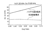
図7は、図6の回路で励磁電流を生成した場合のシミュレーション結果を示す図である。図7(A)はデューティ比を50%にした場合、図7(B)はデューティ比を32%にした場合のシミュレーション結果を示しており、グラフ下の矩形波は、デューティ比を示すための波形である。パルス波形の繰り返し周波数f=31.25kHz、LC共振回路の共振周波数fr=15.65kHzである。このように、図6のトランジスタのベースに異なるデューティ比のパルス波形を供給することで、バイアス直流電流の値を制御した励磁電流を生成することが可能となる。 FIG. 7 is a diagram illustrating a simulation result when an exciting current is generated by the circuit of FIG. FIG. 7A shows a simulation result when the duty ratio is set to 50%, and FIG. 7B shows a simulation result when the duty ratio is set to 32%. It is a waveform. The repetition frequency f of the pulse waveform is 31.25 kHz, and the resonance frequency fr of the LC resonance circuit is 15.65 kHz. In this manner, by supplying pulse waveforms having different duty ratios to the base of the transistor in FIG. 6, it is possible to generate an exciting current in which the value of the bias DC current is controlled.
図8は、図6の回路においてパルス波形のデューティ比を変えた場合のバイアス直流電流と交流励磁電流のそれぞれの電流をシミュレーションした結果を示す図である。図8に示すように、デューティ比を大きくするに伴ってバイアス直流電流が増加している。つまり、図6の回路におけるパルス波形のデューティ比を調整することで、オフセットをゼロにすることができるバイアス直流電流を通電することが可能であることが明確である。なお、図8のグラフにおいて、交流励磁電流はほぼ一定に保たれている。 FIG. 8 is a diagram showing a result of simulating the bias DC current and the AC exciting current when the duty ratio of the pulse waveform is changed in the circuit of FIG. As shown in FIG. 8, the bias DC current increases as the duty ratio increases. In other words, it is clear that by adjusting the duty ratio of the pulse waveform in the circuit of FIG. 6, a bias DC current that can make the offset zero can be supplied. In the graph of FIG. 8, the AC exciting current is kept almost constant.
図7及び図8のシミュレーション結果から、図6に示す回路構成でバイアス直流電流及び交流励磁電流の値をパルス波形のデューティ比で制御することが可能であることがわかる。このように電流値が制御されたバイアス直流電流及び交流励磁電流を極性の切り替えのタイミングで正のオフセット値及び負のオフセット値を打ち消すように供給することで、オフセットをゼロにして高性能な磁界センサを実現することができる。 From the simulation results of FIGS. 7 and 8, it is understood that the values of the bias DC current and the AC exciting current can be controlled by the duty ratio of the pulse waveform with the circuit configuration shown in FIG. By supplying the bias DC current and the AC exciting current whose current values are controlled in such a manner as to cancel the positive offset value and the negative offset value at the timing of the polarity switching, the offset is reduced to zero and the high-performance magnetic field is supplied. A sensor can be realized.
なお、図6の回路において、抵抗R1や抵抗R2の値を調整することで、励磁電流の増減を制御することが可能である。また、パルス波形の繰り返し周波数は、回路中のLC共振回路の共振周波数の1.5倍以上、好ましくは、2〜3倍の間とするのが望ましい。 In the circuit of FIG. 6, it is possible to control the increase or decrease of the exciting current by adjusting the values of the resistors R1 and R2. Further, it is desirable that the repetition frequency of the pulse waveform is 1.5 times or more, preferably 2 to 3 times the resonance frequency of the LC resonance circuit in the circuit.
図6の回路においてパルス波形のデューティ比を制御する場合の処理について、より詳細に説明する。図9は、図6の回路におけるパルス波形を生成する場合のタイミングチャートを示す図である。図9(A)において、タイマーICにより交流励磁電流の周波数の2倍の繰り返し周波数でパルスが出力される。パルス生成手段は、図9(B)に示すように、タイマーICの出力に合わせて矩形波を生成する。このとき、例えば図9(A)の波形の立ち上がりに同期して変化するTフリップフロップを利用して矩形波を生成することができる。また、図9(C)に示すように、図9(B)で生成された矩形波からランプ波(のこぎり波)を生成する。ランプ波は、例えば定電流回路でコンデンサを充電し、図9(B)の立ち上がりのタイミングで当該コンデンサを放電することで生成することが可能である。図9(C)で生成されたランプ波に対して閾値Thを設定し、この閾値Thに基づいて異なるデューティ比の矩形波が生成される(図9(D)、(E))。 Processing for controlling the duty ratio of a pulse waveform in the circuit of FIG. 6 will be described in more detail. FIG. 9 is a diagram showing a timing chart when a pulse waveform is generated in the circuit of FIG. In FIG. 9A, a pulse is output by the timer IC at a repetition frequency twice the frequency of the AC exciting current. The pulse generating means generates a rectangular wave according to the output of the timer IC, as shown in FIG. At this time, for example, a rectangular wave can be generated using a T flip-flop that changes in synchronization with the rise of the waveform in FIG. Also, as shown in FIG. 9C, a ramp wave (saw wave) is generated from the rectangular wave generated in FIG. 9B. The ramp wave can be generated by, for example, charging a capacitor with a constant current circuit and discharging the capacitor at the rising timing in FIG. 9B. A threshold value Th is set for the ramp wave generated in FIG. 9C, and rectangular waves having different duty ratios are generated based on the threshold value Th (FIGS. 9D and 9E).
なお、図4の回路図において、PSD17に入力される同期信号は、図9(B)で生成されたパルス波形となる。また、このとき位相シフトする必要がある場合は、図9(B)の波形をデューティ比D=0.5を維持したまま時間的に遅らせる。例えば、図9(A)の波形を単安定マルチバイブレータに入力し、単安定マルチバイブレータの出力の後端で第2のTフリップフロップを駆動し、その出力をPSD17に加えるようにしてもよい。
Note that, in the circuit diagram of FIG. 4, the synchronization signal input to the
例えば、図9(D)の場合は、閾値Thが高めに設定されており、閾値Thとランプ波とを入力とするコンパレータを用いて、閾値Thがランプ波形よりも高い場合にハイレベルとなる矩形波が生成されている。図9(E)の場合も図9(D)の場合と同様であるが、閾値Thが図9(D)の場合よりも低めに設定されているため、パルス波形のデューティ比が異なるものとなっている。このように閾値Thを調整することでパルス波形のデューティ比を簡単な回路で容易に調整することができる。 For example, in the case of FIG. 9 (D), the threshold value Th is set to a high value, and a high level is obtained when the threshold value Th is higher than the ramp waveform by using a comparator that inputs the threshold value Th and the ramp wave. A square wave has been generated. The case of FIG. 9 (E) is the same as that of FIG. 9 (D) except that the threshold value Th is set lower than in the case of FIG. 9 (D), so that the duty ratio of the pulse waveform is different. Has become. By adjusting the threshold value Th in this manner, the duty ratio of the pulse waveform can be easily adjusted with a simple circuit.
図7のシミュレーション結果において説明したように、図6の回路においてパルス波形のデューティ比を調整することで、バイアス直流電流の大きさを制御することが可能となる。つまり、図3に示したように、オフセットが等価となる正のバイアス直流電流と負のバイアス直流電流とは、それぞれ絶対値が異なるため、各極性におけるオフセットを打ち消すような電流が供給されるように図6のパルス生成手段がパルス波形を生成する。このとき、図9に示したように、ランプ波形と比較する閾値Thを調整することで、パルス波形のデューティ比を調整し、このデューティ比に対応した大きさの電流値を正極性及び負極性のそれぞれにおいて供給することで、オフセットをゼロとする非常に高性能な磁界センサを実現することが可能となる。 As described in the simulation result of FIG. 7, the magnitude of the bias DC current can be controlled by adjusting the duty ratio of the pulse waveform in the circuit of FIG. That is, as shown in FIG. 3, since the positive bias DC current and the negative bias DC current having the equivalent offset have different absolute values, a current is supplied so as to cancel the offset in each polarity. Next, the pulse generation means of FIG. 6 generates a pulse waveform. At this time, as shown in FIG. 9, the duty ratio of the pulse waveform is adjusted by adjusting the threshold value Th to be compared with the ramp waveform, and the current value having a magnitude corresponding to the duty ratio is adjusted to the positive polarity and the negative polarity. , It is possible to realize a very high performance magnetic field sensor having an offset of zero.
なお、図9に示したランプ波はこれに限らず、一周期の間で時間の変化と共に出力が変化する、すなわち閾値Thから時間に変換可能な波形であればよい。例えば、時間と共に単調に増加又は減少する波形や、時間と共に変化する単峰性を有する波形を用いることが可能である。 Note that the ramp wave shown in FIG. 9 is not limited to this, and any waveform may be used as long as the output changes with time during one cycle, that is, a waveform that can be converted from the threshold value Th to time. For example, it is possible to use a waveform that monotonically increases or decreases with time or a waveform that has a monomodal property that changes with time.
また、本実施形態においては、正のバイアス直流電流を通電した場合に生じるオフセット値と、負のバイアス直流電流を通電した場合に生じるオフセット値とが等価となる正及び負のバイアス直流電流値を計測手段で計測し、電流供給部41が、バイアス用の直流電流の値を計測手段で計測された正及び負のバイアス直流電流値に自動調整する構成としてもよい。
In the present embodiment, an offset value generated when a positive bias DC current is supplied and an offset value generated when a negative bias DC current is supplied are equivalent to positive and negative bias DC current values. The
このように、本実施形態に係る磁界センサにおいては、矩形パルス波形を元に直流電流でバイアスされた交番電圧波形を生成し、前記矩形パルス波形のディーティ比に応じて前記バイアス用の直流電流の値を制御するため、オフセットをゼロにすることができると共に、回路構成を簡単にすることができる。 As described above, in the magnetic field sensor according to the present embodiment, the alternating voltage waveform biased with the DC current is generated based on the rectangular pulse waveform, and the bias DC current is generated according to the duty ratio of the rectangular pulse waveform. Since the value is controlled, the offset can be made zero and the circuit configuration can be simplified.
なお、上記各実施の形態に示した構成以外に、その他の実施の形態として以下に説明する。例えば、前記第1の実施形態に示した図1の回路図における検出回路16と、第2の実施形態における図4や図6に示した電流供給部41の回路とを組み合わせて本発明の磁界センサを実現することが可能である。
In addition, other embodiments than the configuration shown in each of the above embodiments will be described below. For example, a combination of the
具体的には、まず図9(E)の波形について、ハイレベルとローレベルを反転する。図10は、図6の回路においてパルス波形のハイレベルとローレベルとを反転した場合の正弦波を示す図である。図10に示すように、パルス波形のハイレベルとローレベルを反転することで、正弦波成分もパルス波形に応じて反転する。 Specifically, first, the waveform of FIG. 9E is inverted between a high level and a low level. FIG. 10 is a diagram showing a sine wave when the high level and the low level of the pulse waveform are inverted in the circuit of FIG. As shown in FIG. 10, by inverting the high level and the low level of the pulse waveform, the sine wave component is also inverted according to the pulse waveform.
そして、反転した後のパルス波形において、デューティ比を直流電源10aの電圧が供給するバイアス直流電流の大きさになるよう調整する。このように調整した波形を仮にE’とし、バイアス直流電流の極性切り替えは図9(D)の波形とE’の波形を図4の切り替え方法を用いて行う。図11は、図9(D)に相当する波形のデューティ比を0.33、E’に相当する波形のデューティ比を0.67とした場合の励磁電流の波形を示す図である。このようにE’の波形においてパルス波形を反転した場合に正弦波の位相も反転していることがわかる。つまり、交流励磁電流への影響なくバイアス直流電流を調整することが可能である。
Then, in the inverted pulse waveform, the duty ratio is adjusted so as to be equal to the magnitude of the bias DC current supplied by the voltage of the
その他の実施形態において、このような構成にすることで、必要なバイアス直流電流idc1及びidc2を磁気コア15に供給し、交流励磁電流の反転は、あらかじめ正弦波成分を反転させていたE’の波形を用いることで反転が2度生じ、本発明に係る磁界センサの動作を行うことが可能となる。
In another embodiment, by adopting such a configuration, necessary bias DC currents idc1 and idc2 are supplied to the
以下、本発明に係る付記を示す。本発明に係る磁界センサは、必要に応じて、磁気コアに検出コイルを巻回して形成されるセンサヘッドと、前記磁気コアに励磁用の交流電流及びバイアス用の直流電流を重畳させて供給する電流供給手段と、少なくとも前記バイアス用の直流電流の極性を切り替える切替手段と、前記検出コイルに接続され、前記センサヘッドで測定された磁界をフィードバック電流で検出する検出回路とを備え、前記切替手段が前記直流電流の極性を正極性に切り替えた場合に、正のバイアス直流電流を通電したときに生じるオフセット値と、負のバイアス直流電流を通電したときに生じるオフセット値とが等価となる正のバイアス直流電流値及び負のバイアス直流電流値のうち、前記正のバイアス直流電流値が前記電流供給手段により前記磁気コアに供給され、前記切替手段が前記直流電流の極性を負極性に切り替えた場合には、前記負のバイアス直流電流値が前記電流供給手段により前記磁気コアに供給されるものである。Hereinafter, additional notes according to the present invention will be shown. The magnetic field sensor according to the present invention supplies a sensor head formed by winding a detection coil around a magnetic core, and an excitation AC current and a bias DC current superimposed on the magnetic core, if necessary. Current supply means, switching means for switching at least the polarity of the DC current for bias, and a detection circuit connected to the detection coil and detecting a magnetic field measured by the sensor head with a feedback current, the switching means When the polarity of the DC current is switched to a positive polarity, an offset value generated when a positive bias DC current is applied is equal to an offset value generated when a negative bias DC current is applied. Of the bias DC current value and the negative bias DC current value, the positive bias DC current value is supplied to the magnetic core by the current supply means. Is, when the switching means switches the polarity of the direct current negative polarity is to the negative bias DC current value is supplied to the magnetic core by the current supply means.
このように、本発明に係る磁界センサにおいては、バイアス直流電流の極性を正極性に切り替えた場合に、正のバイアス直流電流を通電したときに生じるオフセット値と、負のバイアス直流電流を通電したときに生じるオフセット値とが等価となる正のバイアス直流電流値及び負のバイアス直流電流値のうち、正のバイアス直流電流値が磁気コアに供給され、バイアス直流電流の極性を負極性に切り替えた場合には、負のバイアス直流電流値が磁気コアに供給されるため、バイアス直流電流が正極の場合と負極の場合とで、それぞれオフセットが等しく、バイアス電流が正又は負の時の出力のいずれか一方の極性を反転して平滑フィルタにおいて加算される時、オフセットが差っ引かれるようにバイアス直流電流値が制御され、オフセットをゼロにすることができるという効果を奏する。Thus, in the magnetic field sensor according to the present invention, when the polarity of the bias DC current is switched to the positive polarity, the offset value generated when the positive bias DC current is applied and the negative bias DC current are applied. Of the positive bias DC current value and the negative bias DC current value that are equivalent to the offset value that occurs when the positive bias DC current value is supplied to the magnetic core, the polarity of the bias DC current is switched to negative polarity In such a case, since the negative bias DC current value is supplied to the magnetic core, the offset is equal between the case where the bias DC current is positive and the case where the bias DC current is negative, and either the output when the bias current is positive or negative is output. When the polarity is inverted and added in the smoothing filter, the bias DC current value is controlled so that the offset is subtracted, and the offset is reduced. An effect that can be filtered.
本発明に係る磁界センサは、必要に応じて、前記電流供給手段が、前記正のバイアス直流電流を供給する第1直流電源と、前記負のバイアス直流電流を供給する第2直流電源と、前記交流電流を供給する交流電源と、前記第1直流電源が供給する正のバイアス直流電流又は前記第2直流電源が供給する負のバイアス直流電流と、前記交流電流とを加算して励磁電流を生成する加算手段とを有しており、前記励磁電流の極性を切り替える第2切替手段を備えるものである。In the magnetic field sensor according to the present invention, if necessary, the current supply means supplies a first DC power supply for supplying the positive bias DC current, a second DC power supply for supplying the negative bias DC current, An excitation current is generated by adding an AC power supply that supplies an AC current, a positive bias DC current supplied by the first DC power supply or a negative bias DC current supplied by the second DC power supply, and the AC current. And second switching means for switching the polarity of the exciting current.
このように、本発明に係る磁界センサにおいては、前記電流供給手段が、前記正のバイアス直流電流を供給する第1直流電源と、前記負のバイアス直流電流を供給する第2直流電源と、前記交流電流を供給する交流電源と、前記正のバイアス直流電流又は前記負のバイアス直流電流と、前記交流電流とを加算して励磁電流を生成する加算手段とを有しており、前記励磁電流の極性を切り替える第2切替手段を備えるため、正又は負のオフセットに応じて当該オフセットを打ち消すように正又は負のバイアス直流電流を切り替えて磁気コアに供給することができ、オフセットをゼロにすることができるという効果を奏する。As described above, in the magnetic field sensor according to the present invention, the current supply unit includes the first DC power supply that supplies the positive bias DC current, the second DC power supply that supplies the negative bias DC current, An AC power supply that supplies an AC current; and an adding unit that generates an exciting current by adding the positive bias DC current or the negative bias DC current and the AC current. Since the second switching means for switching the polarity is provided, a positive or negative bias DC current can be switched and supplied to the magnetic core so as to cancel the offset in accordance with the positive or negative offset, and the offset can be made zero. This has the effect that it can be performed.
本発明に係る磁界センサは、必要に応じて、前記電流供給手段が、矩形パルス波形を元に直流電流でバイアスされた交番電圧波形を生成し、前記矩形パルス波形のディーティ比に応じて前記バイアス用の直流電流の値を制御するものである。In the magnetic field sensor according to the present invention, if necessary, the current supply unit generates an alternating voltage waveform biased with a DC current based on a rectangular pulse waveform, and the bias is generated according to a duty ratio of the rectangular pulse waveform. To control the value of the DC current for use.
このように、本発明に係る磁界センサにおいては、矩形パルス波形を元に直流電流でバイアスされた交番電圧波形を生成し、前記矩形パルス波形のディーティ比に応じて前記バイアス用の直流電流の値を制御するため、例えば、非特許文献2に示すような誤差増幅後の電圧値の加算等の処理やその回路が不要となり、回路を簡単にすることができると共に、オフセットをゼロにすることができるという効果を奏する。As described above, in the magnetic field sensor according to the present invention, the alternating voltage waveform biased with the DC current is generated based on the rectangular pulse waveform, and the value of the bias DC current is determined according to the duty ratio of the rectangular pulse waveform. Therefore, for example, processing such as addition of a voltage value after error amplification as shown in
本発明に係る磁界センサは、必要に応じて、前記電流供給手段が、前記磁気コアに供給する交流電流の半分の周期で矩形パルス波形を生成する矩形パルス波形生成手段と、生成された矩形パルス波形に基づいて、一周期の間で時間の変化と共に出力が変化する周期波形を生成する周期波形生成手段と、生成された前記周期波形に対して設定された閾値を調整する閾値調整手段とを備え、前記閾値の変化に伴う前記周期波形の出力変化で前記矩形パルス波形のデューティ比を制御するものである。In the magnetic field sensor according to the present invention, the current supply unit may generate a rectangular pulse waveform at a half cycle of an alternating current supplied to the magnetic core, if necessary. On the basis of the waveform, a periodic waveform generating means for generating a periodic waveform whose output changes with time during one cycle, and threshold adjusting means for adjusting a threshold set for the generated periodic waveform A duty ratio of the rectangular pulse waveform is controlled by an output change of the periodic waveform according to a change of the threshold value.
このように、本発明に係る磁界センサにおいては、磁気コアに供給する交流電流の半分の周期で矩形パルス波形を生成し、生成された矩形パルス波形に基づいて、一周期の間で時間の変化と共に出力が変化する周期波形を生成し、生成された周期波形に対して設定された閾値を調整し、当該閾値の変化に伴う周期波形の出力変化で矩形パルス波形のデューティ比を制御するため、閾値の調整だけで、バイアス直流電流の極性に応じた電流値を制御して通電することができ、回路構成を簡素化することができるという効果を奏する。As described above, in the magnetic field sensor according to the present invention, the rectangular pulse waveform is generated at a half cycle of the alternating current supplied to the magnetic core, and the time change during one cycle is performed based on the generated rectangular pulse waveform. In order to control the duty ratio of the rectangular pulse waveform by adjusting the threshold set for the generated periodic waveform and controlling the duty ratio of the rectangular pulse waveform with the output change of the periodic waveform according to the change of the threshold, Only by adjusting the threshold value, it is possible to control and supply a current value corresponding to the polarity of the bias DC current, so that the circuit configuration can be simplified.
本発明に係る磁界センサは、必要に応じて、正のバイアス直流電流を通電した場合に生じるオフセット値と、負のバイアス直流電流を通電した場合に生じるオフセット値とが等価となる正及び負のバイアス直流電流値を計測する計測手段を備え、前記電流供給手段が、前記バイアス用の直流電流の値を前記計測手段で計測された正及び負のバイアス直流電流値に調整するものである。The magnetic field sensor according to the present invention, if necessary, the positive and negative offset values that occur when a positive bias DC current is applied and the offset value that occurs when a negative bias DC current is applied are equivalent Measuring means for measuring a bias DC current value is provided, and the current supply means adjusts the value of the bias DC current to positive and negative bias DC current values measured by the measuring means.
このように、本発明に係る磁界センサにおいては、正のバイアス直流電流を通電した場合に生じるオフセット値と、負のバイアス直流電流を通電した場合に生じるオフセット値とが等価となる正及び負のバイアス直流電流値を計測し、電流供給手段が、バイアス用の直流電流の値を計測手段で計測された正及び負のバイアス直流電流値に調整するため、オフセットの計測からその調整までを自動化して作業を格段に向上させることができるという効果を奏する。As described above, in the magnetic field sensor according to the present invention, the offset value generated when the positive bias DC current is applied is equal to the offset value generated when the negative bias DC current is applied. The bias DC current value is measured, and the current supply means adjusts the value of the bias DC current to the positive and negative bias DC current values measured by the measurement means. Thus, the operation can be significantly improved.
1 磁界センサ
10(10a,10b) 直流電源
11 第1スイッチ
12 交流電源
13 検出コイル
14 センサヘッド
15 磁性コア
16 検出コイル
17 同期整流器
18,19 回路
20 第2スイッチ
21 第3スイッチ
22 ローパスフィルタ
23 エラーアンプ
24 帰還抵抗
41 電流供給部
42 第4スイッチ
43 バッファ回路
44 プリアンプ回路
51 位相シフタ
Reference Signs List 1 magnetic field sensor 10 (10a, 10b)
Claims (9)
前記トランジスタの後段側で当該トランジスタとグランドとの間に配設され、コンデンサとコイルとが並列接続されるLC共振回路と、An LC resonance circuit disposed between the transistor and the ground at a subsequent stage of the transistor, wherein a capacitor and a coil are connected in parallel;
前記LC共振回路における前記コイルの後段側に接続するための第1端子と、A first terminal for connection to a subsequent stage of the coil in the LC resonance circuit;
前記グランドに接続するための第2端子とを備え、A second terminal for connecting to the ground,
前記第1端子及び前記第2端子間に接続する抵抗体に、交流電流と当該交流電流の振幅よりも大きい値の直流電流とを重畳した電流を供給することを特徴とする電流供給装置。A current supply device, wherein a current obtained by superimposing an alternating current and a direct current having a value larger than the amplitude of the alternating current is supplied to a resistor connected between the first terminal and the second terminal.
前記パルス生成手段が生成するパルス周波数が、前記LC共振回路の共振周波数よりも大きい電流供給装置。 The current supply device according to claim 1,
A current supply device wherein a pulse frequency generated by the pulse generation means is higher than a resonance frequency of the LC resonance circuit.
前記第1端子及び前記第2端子間にセンサヘッドを構成する磁気コアが接続される基本波型直交フラックスゲートとを備える磁界センサ。 A current supply device according to claim 1 or 2,
A magnetic field sensor comprising: a fundamental wave type orthogonal flux gate to which a magnetic core constituting a sensor head is connected between the first terminal and the second terminal .
前記基本波型直交フラックスゲートが、
前記磁気コアに検出コイルを巻回して形成されるセンサヘッドと、
少なくとも前記バイアス用の直流電流の極性を切り替える切替手段と、
前記検出コイルに接続され、前記センサヘッドで測定された磁界をフィードバック電流で検出する検出回路とを備え、
前記切替手段が前記直流電流の極性を正極性に切り替えた場合に、正のバイアス直流電流を通電したときに生じるオフセット値と、負のバイアス直流電流を通電したときに生じるオフセット値とが等価となる正のバイアス直流電流値及び負のバイアス直流電流値のうち、前記正のバイアス直流電流値が前記電流供給装置により前記磁気コアに供給され、
前記切替手段が前記直流電流の極性を負極性に切り替えた場合には、前記負のバイアス直流電流値が前記電流供給装置により前記磁気コアに供給されることを特徴とする磁界センサ。 The magnetic field sensor according to claim 3,
The fundamental wave type orthogonal flux gate,
A sensor head formed by winding a detection coil around the magnetic core;
Switching means for switching at least the polarity of the DC current for bias,
A detection circuit connected to the detection coil and detecting a magnetic field measured by the sensor head by a feedback current ,
When the switching unit switches the polarity of the DC current to a positive polarity, an offset value generated when a positive bias DC current is applied is equivalent to an offset value generated when a negative bias DC current is applied. Among the positive bias DC current value and the negative bias DC current value, the positive bias DC current value is supplied to the magnetic core by the current supply device,
The magnetic field sensor according to claim 1, wherein when the switching unit switches the polarity of the DC current to a negative polarity, the negative bias DC current value is supplied to the magnetic core by the current supply device .
前記電流供給装置が、矩形パルス波形を元に直流電流でバイアスされた交番電圧波形を生成し、前記矩形パルス波形のディーティ比に応じて前記バイアス用の直流電流の値を制御する磁界センサ。 The magnetic field sensor according to claim 4 ,
A magnetic field sensor , wherein the current supply device generates an alternating voltage waveform biased with a DC current based on a rectangular pulse waveform, and controls a value of the DC current for bias according to a duty ratio of the rectangular pulse waveform .
前記電流供給装置が、The current supply device,
前記磁気コアに供給する交流電流の半分の周期で矩形パルス波形を生成する矩形パルス波形生成手段と、Rectangular pulse waveform generating means for generating a rectangular pulse waveform with a half cycle of the alternating current supplied to the magnetic core,
生成された矩形パルス波形に基づいて、一周期の間で時間の変化と共に出力が変化する周期波形を生成する周期波形生成手段と、A periodic waveform generating unit that generates a periodic waveform whose output changes with time during one cycle based on the generated rectangular pulse waveform;
生成された前記周期波形に対して設定された閾値を調整する閾値調整手段とを備え、Threshold adjusting means for adjusting a threshold set for the generated periodic waveform,
前記閾値の変化に伴う前記周期波形の出力変化で前記矩形パルス波形のデューティ比を制御する磁界センサ。A magnetic field sensor for controlling a duty ratio of the rectangular pulse waveform by an output change of the periodic waveform according to a change of the threshold value.
正のバイアス直流電流を通電した場合に生じるオフセット値と、負のバイアス直流電流を通電した場合に生じるオフセット値とが等価となる正及び負のバイアス直流電流値を計測する計測手段を備え、Measuring means for measuring a positive and negative bias DC current value in which an offset value generated when a positive bias DC current is supplied and an offset value generated when a negative bias DC current is supplied are equivalent,
前記電流供給装置が、前記バイアス用の直流電流の値を前記計測手段で計測された正及び負のバイアス直流電流値に調整する磁界センサ。A magnetic field sensor, wherein the current supply device adjusts the value of the bias DC current to positive and negative bias DC current values measured by the measuring unit.
前記磁気コアに励磁用の交流電流及びバイアス用の直流電流を重畳させて供給する電流供給手段と、Current supply means for supplying an alternating current for excitation and a direct current for bias superimposed on the magnetic core;
少なくとも前記バイアス用の直流電流の極性を切り替える切替手段と、Switching means for switching at least the polarity of the DC current for bias,
前記検出コイルに接続され、前記センサヘッドで測定された磁界をフィードバック電流で検出する検出回路とを備え、A detection circuit connected to the detection coil and detecting a magnetic field measured by the sensor head by a feedback current,
前記切替手段が前記直流電流の極性を正極性に切り替えた場合に、正のバイアス直流電流を通電したときに生じるオフセット値と、負のバイアス直流電流を通電したときに生じるオフセット値とが等価となる正のバイアス直流電流値及び負のバイアス直流電流値のうち、前記正のバイアス直流電流値が前記電流供給手段により前記磁気コアに供給され、When the switching unit switches the polarity of the DC current to a positive polarity, an offset value generated when a positive bias DC current is applied is equivalent to an offset value generated when a negative bias DC current is applied. Among the positive bias DC current value and the negative bias DC current value, the positive bias DC current value is supplied to the magnetic core by the current supply unit,
前記切替手段が前記直流電流の極性を負極性に切り替えた場合には、前記負のバイアス直流電流値が前記電流供給手段により前記磁気コアに供給されることを特徴とする磁界センサ。The magnetic field sensor according to claim 1, wherein when the switching unit switches the polarity of the DC current to a negative polarity, the negative bias DC current value is supplied to the magnetic core by the current supply unit.
前記電流供給手段が、The current supply means,
前記正のバイアス直流電流を供給する第1直流電源と、A first DC power supply that supplies the positive bias DC current;
前記負のバイアス直流電流を供給する第2直流電源と、A second DC power supply that supplies the negative bias DC current;
前記交流電流を供給する交流電源と、An AC power supply for supplying the AC current;
前記第1直流電源が供給する正のバイアス直流電流又は前記第2直流電源が供給する前記負のバイアス直流電流と、前記交流電流とを加算して励磁電流を生成する加算手段とを有しており、A positive bias DC current supplied by the first DC power supply or a negative bias DC current supplied by the second DC power supply, and an adding means for adding the AC current to generate an exciting current; Yes,
前記励磁電流の極性を切り替える第2切替手段を備える磁界センサ。A magnetic field sensor comprising second switching means for switching the polarity of the exciting current.
Priority Applications (1)
| Application Number | Priority Date | Filing Date | Title |
|---|---|---|---|
| JP2018110718A JP2019211450A (en) | 2018-06-08 | 2018-06-08 | Magnetic field sensor |
Applications Claiming Priority (1)
| Application Number | Priority Date | Filing Date | Title |
|---|---|---|---|
| JP2018110718A JP2019211450A (en) | 2018-06-08 | 2018-06-08 | Magnetic field sensor |
Publications (2)
| Publication Number | Publication Date |
|---|---|
| JP2019211450A JP2019211450A (en) | 2019-12-12 |
| JP2019211450A5 true JP2019211450A5 (en) | 2020-04-02 |
Family
ID=68846735
Family Applications (1)
| Application Number | Title | Priority Date | Filing Date |
|---|---|---|---|
| JP2018110718A Pending JP2019211450A (en) | 2018-06-08 | 2018-06-08 | Magnetic field sensor |
Country Status (1)
| Country | Link |
|---|---|
| JP (1) | JP2019211450A (en) |
Families Citing this family (2)
| Publication number | Priority date | Publication date | Assignee | Title |
|---|---|---|---|---|
| JP7074368B2 (en) * | 2020-03-26 | 2022-05-24 | 国立研究開発法人宇宙航空研究開発機構 | Fluxgate magnetic field sensor |
| JP7025813B1 (en) * | 2021-10-14 | 2022-02-25 | 笹田磁気計測研究所株式会社 | Current supply device and magnetic sensor |
Family Cites Families (6)
| Publication number | Priority date | Publication date | Assignee | Title |
|---|---|---|---|---|
| JPS6265187A (en) * | 1985-09-17 | 1987-03-24 | 松下電器産業株式会社 | Coin detector |
| JP3374590B2 (en) * | 1995-03-31 | 2003-02-04 | 株式会社島津製作所 | Magnetometer |
| JP4209114B2 (en) * | 2002-01-21 | 2009-01-14 | 株式会社産学連携機構九州 | Magnetic field sensor |
| JP4732705B2 (en) * | 2004-04-30 | 2011-07-27 | 独立行政法人科学技術振興機構 | Magnetic field sensor |
| US8237438B2 (en) * | 2009-03-13 | 2012-08-07 | Quantec Geoscience | Very low noise magnetometer |
| JP2013156207A (en) * | 2012-01-31 | 2013-08-15 | Semiconductor Components Industries Llc | Flow measurement device of fluid |
-
2018
- 2018-06-08 JP JP2018110718A patent/JP2019211450A/en active Pending
Similar Documents
| Publication | Publication Date | Title |
|---|---|---|
| EP3121609B1 (en) | Direct-current residual-current detecting device | |
| JP5364816B1 (en) | Magnetic element control device, magnetic element control method, and magnetic detection device | |
| JP5364814B2 (en) | Magnetic element control device, magnetic element control method, and magnetic detection device | |
| JP5393844B2 (en) | Magnetic element control device, magnetic element control method, and magnetic detection device | |
| JP2011017618A (en) | Electric current sensor | |
| WO2014010187A1 (en) | Current detection device | |
| JP6885538B2 (en) | Magnetic field sensor | |
| JP2017502302A (en) | Resonant impedance sensing with negative impedance control loop | |
| JP2019211450A5 (en) | ||
| WO2001006266A1 (en) | Ac current detection device | |
| JP2019211450A (en) | Magnetic field sensor | |
| JP2020126016A (en) | Flux gate magnetic field sensor and method for adjusting the same | |
| JP2022549382A (en) | fluxgate current converter | |
| JP5702592B2 (en) | Current detector | |
| JP6823878B2 (en) | Fluxgate magnetic field sensor | |
| JP3161133B2 (en) | Force detection device | |
| JP2014071101A (en) | Signal processing circuit and magnetic field detection device using the same | |
| JPS6057277A (en) | Self-excitation type magnetism detecting method | |
| WO2015104776A1 (en) | Current detection device | |
| JP6229243B2 (en) | Current detector | |
| JP6043606B2 (en) | Magnetic element control device, magnetic element control method, and magnetic detection device | |
| JP7289987B2 (en) | How to Reduce Noise in Fluxgate Current Transducers | |
| JP2015121424A (en) | Magnetic element control device, magnetic element control method, and magnetic detector | |
| JP3583699B2 (en) | Sensor device | |
| JP7074368B2 (en) | Fluxgate magnetic field sensor |