JP2019201075A - Substrate processing apparatus and substrate processing method - Google Patents
Substrate processing apparatus and substrate processing method Download PDFInfo
- Publication number
- JP2019201075A JP2019201075A JP2018093939A JP2018093939A JP2019201075A JP 2019201075 A JP2019201075 A JP 2019201075A JP 2018093939 A JP2018093939 A JP 2018093939A JP 2018093939 A JP2018093939 A JP 2018093939A JP 2019201075 A JP2019201075 A JP 2019201075A
- Authority
- JP
- Japan
- Prior art keywords
- substrate
- processing
- liquid
- top plate
- wafer
- Prior art date
- Legal status (The legal status is an assumption and is not a legal conclusion. Google has not performed a legal analysis and makes no representation as to the accuracy of the status listed.)
- Granted
Links
Images


Classifications
-
- H—ELECTRICITY
- H01—ELECTRIC ELEMENTS
- H01L—SEMICONDUCTOR DEVICES NOT COVERED BY CLASS H10
- H01L21/00—Processes or apparatus adapted for the manufacture or treatment of semiconductor or solid state devices or of parts thereof
- H01L21/67—Apparatus specially adapted for handling semiconductor or electric solid state devices during manufacture or treatment thereof; Apparatus specially adapted for handling wafers during manufacture or treatment of semiconductor or electric solid state devices or components ; Apparatus not specifically provided for elsewhere
- H01L21/67005—Apparatus not specifically provided for elsewhere
- H01L21/67011—Apparatus for manufacture or treatment
- H01L21/67155—Apparatus for manufacturing or treating in a plurality of work-stations
- H01L21/6719—Apparatus for manufacturing or treating in a plurality of work-stations characterized by the construction of the processing chambers, e.g. modular processing chambers
-
- B—PERFORMING OPERATIONS; TRANSPORTING
- B05—SPRAYING OR ATOMISING IN GENERAL; APPLYING FLUENT MATERIALS TO SURFACES, IN GENERAL
- B05C—APPARATUS FOR APPLYING FLUENT MATERIALS TO SURFACES, IN GENERAL
- B05C11/00—Component parts, details or accessories not specifically provided for in groups B05C1/00 - B05C9/00
- B05C11/02—Apparatus for spreading or distributing liquids or other fluent materials already applied to a surface ; Controlling means therefor; Control of the thickness of a coating by spreading or distributing liquids or other fluent materials already applied to the coated surface
- B05C11/023—Apparatus for spreading or distributing liquids or other fluent materials already applied to a surface
-
- F—MECHANICAL ENGINEERING; LIGHTING; HEATING; WEAPONS; BLASTING
- F26—DRYING
- F26B—DRYING SOLID MATERIALS OR OBJECTS BY REMOVING LIQUID THEREFROM
- F26B21/00—Arrangements or duct systems, e.g. in combination with pallet boxes, for supplying and controlling air or gases for drying solid materials or objects
- F26B21/02—Circulating air or gases in closed cycles, e.g. wholly within the drying enclosure
- F26B21/022—Circulating air or gases in closed cycles, e.g. wholly within the drying enclosure with provisions for changing the drying gas flow pattern, e.g. by reversing gas flow, by moving the materials or objects through subsequent compartments, at least two of which have a different direction of gas flow
- F26B21/028—Circulating air or gases in closed cycles, e.g. wholly within the drying enclosure with provisions for changing the drying gas flow pattern, e.g. by reversing gas flow, by moving the materials or objects through subsequent compartments, at least two of which have a different direction of gas flow by air valves, movable baffles or nozzle arrangements
-
- H—ELECTRICITY
- H01—ELECTRIC ELEMENTS
- H01L—SEMICONDUCTOR DEVICES NOT COVERED BY CLASS H10
- H01L21/00—Processes or apparatus adapted for the manufacture or treatment of semiconductor or solid state devices or of parts thereof
- H01L21/02—Manufacture or treatment of semiconductor devices or of parts thereof
- H01L21/02041—Cleaning
- H01L21/02057—Cleaning during device manufacture
-
- H—ELECTRICITY
- H01—ELECTRIC ELEMENTS
- H01L—SEMICONDUCTOR DEVICES NOT COVERED BY CLASS H10
- H01L21/00—Processes or apparatus adapted for the manufacture or treatment of semiconductor or solid state devices or of parts thereof
- H01L21/02—Manufacture or treatment of semiconductor devices or of parts thereof
- H01L21/02104—Forming layers
- H01L21/02107—Forming insulating materials on a substrate
- H01L21/02296—Forming insulating materials on a substrate characterised by the treatment performed before or after the formation of the layer
- H01L21/02299—Forming insulating materials on a substrate characterised by the treatment performed before or after the formation of the layer pre-treatment
- H01L21/02307—Forming insulating materials on a substrate characterised by the treatment performed before or after the formation of the layer pre-treatment treatment by exposure to a liquid
-
- H—ELECTRICITY
- H01—ELECTRIC ELEMENTS
- H01L—SEMICONDUCTOR DEVICES NOT COVERED BY CLASS H10
- H01L21/00—Processes or apparatus adapted for the manufacture or treatment of semiconductor or solid state devices or of parts thereof
- H01L21/02—Manufacture or treatment of semiconductor devices or of parts thereof
- H01L21/02104—Forming layers
- H01L21/02107—Forming insulating materials on a substrate
- H01L21/02296—Forming insulating materials on a substrate characterised by the treatment performed before or after the formation of the layer
- H01L21/02318—Forming insulating materials on a substrate characterised by the treatment performed before or after the formation of the layer post-treatment
- H01L21/02343—Forming insulating materials on a substrate characterised by the treatment performed before or after the formation of the layer post-treatment treatment by exposure to a liquid
-
- H—ELECTRICITY
- H01—ELECTRIC ELEMENTS
- H01L—SEMICONDUCTOR DEVICES NOT COVERED BY CLASS H10
- H01L21/00—Processes or apparatus adapted for the manufacture or treatment of semiconductor or solid state devices or of parts thereof
- H01L21/02—Manufacture or treatment of semiconductor devices or of parts thereof
- H01L21/04—Manufacture or treatment of semiconductor devices or of parts thereof the devices having at least one potential-jump barrier or surface barrier, e.g. PN junction, depletion layer or carrier concentration layer
- H01L21/18—Manufacture or treatment of semiconductor devices or of parts thereof the devices having at least one potential-jump barrier or surface barrier, e.g. PN junction, depletion layer or carrier concentration layer the devices having semiconductor bodies comprising elements of Group IV of the Periodic System or AIIIBV compounds with or without impurities, e.g. doping materials
- H01L21/30—Treatment of semiconductor bodies using processes or apparatus not provided for in groups H01L21/20 - H01L21/26
- H01L21/302—Treatment of semiconductor bodies using processes or apparatus not provided for in groups H01L21/20 - H01L21/26 to change their surface-physical characteristics or shape, e.g. etching, polishing, cutting
- H01L21/306—Chemical or electrical treatment, e.g. electrolytic etching
- H01L21/30604—Chemical etching
-
- H—ELECTRICITY
- H01—ELECTRIC ELEMENTS
- H01L—SEMICONDUCTOR DEVICES NOT COVERED BY CLASS H10
- H01L21/00—Processes or apparatus adapted for the manufacture or treatment of semiconductor or solid state devices or of parts thereof
- H01L21/67—Apparatus specially adapted for handling semiconductor or electric solid state devices during manufacture or treatment thereof; Apparatus specially adapted for handling wafers during manufacture or treatment of semiconductor or electric solid state devices or components ; Apparatus not specifically provided for elsewhere
- H01L21/67005—Apparatus not specifically provided for elsewhere
- H01L21/67011—Apparatus for manufacture or treatment
- H01L21/67017—Apparatus for fluid treatment
- H01L21/67028—Apparatus for fluid treatment for cleaning followed by drying, rinsing, stripping, blasting or the like
- H01L21/6704—Apparatus for fluid treatment for cleaning followed by drying, rinsing, stripping, blasting or the like for wet cleaning or washing
- H01L21/67051—Apparatus for fluid treatment for cleaning followed by drying, rinsing, stripping, blasting or the like for wet cleaning or washing using mainly spraying means, e.g. nozzles
-
- H—ELECTRICITY
- H01—ELECTRIC ELEMENTS
- H01L—SEMICONDUCTOR DEVICES NOT COVERED BY CLASS H10
- H01L21/00—Processes or apparatus adapted for the manufacture or treatment of semiconductor or solid state devices or of parts thereof
- H01L21/67—Apparatus specially adapted for handling semiconductor or electric solid state devices during manufacture or treatment thereof; Apparatus specially adapted for handling wafers during manufacture or treatment of semiconductor or electric solid state devices or components ; Apparatus not specifically provided for elsewhere
- H01L21/67005—Apparatus not specifically provided for elsewhere
- H01L21/67011—Apparatus for manufacture or treatment
- H01L21/6715—Apparatus for applying a liquid, a resin, an ink or the like
-
- H—ELECTRICITY
- H01—ELECTRIC ELEMENTS
- H01L—SEMICONDUCTOR DEVICES NOT COVERED BY CLASS H10
- H01L21/00—Processes or apparatus adapted for the manufacture or treatment of semiconductor or solid state devices or of parts thereof
- H01L21/67—Apparatus specially adapted for handling semiconductor or electric solid state devices during manufacture or treatment thereof; Apparatus specially adapted for handling wafers during manufacture or treatment of semiconductor or electric solid state devices or components ; Apparatus not specifically provided for elsewhere
- H01L21/67005—Apparatus not specifically provided for elsewhere
- H01L21/67011—Apparatus for manufacture or treatment
- H01L21/67155—Apparatus for manufacturing or treating in a plurality of work-stations
- H01L21/67161—Apparatus for manufacturing or treating in a plurality of work-stations characterized by the layout of the process chambers
- H01L21/67173—Apparatus for manufacturing or treating in a plurality of work-stations characterized by the layout of the process chambers in-line arrangement
-
- H—ELECTRICITY
- H01—ELECTRIC ELEMENTS
- H01L—SEMICONDUCTOR DEVICES NOT COVERED BY CLASS H10
- H01L21/00—Processes or apparatus adapted for the manufacture or treatment of semiconductor or solid state devices or of parts thereof
- H01L21/67—Apparatus specially adapted for handling semiconductor or electric solid state devices during manufacture or treatment thereof; Apparatus specially adapted for handling wafers during manufacture or treatment of semiconductor or electric solid state devices or components ; Apparatus not specifically provided for elsewhere
- H01L21/67005—Apparatus not specifically provided for elsewhere
- H01L21/67242—Apparatus for monitoring, sorting or marking
-
- H—ELECTRICITY
- H01—ELECTRIC ELEMENTS
- H01L—SEMICONDUCTOR DEVICES NOT COVERED BY CLASS H10
- H01L21/00—Processes or apparatus adapted for the manufacture or treatment of semiconductor or solid state devices or of parts thereof
- H01L21/67—Apparatus specially adapted for handling semiconductor or electric solid state devices during manufacture or treatment thereof; Apparatus specially adapted for handling wafers during manufacture or treatment of semiconductor or electric solid state devices or components ; Apparatus not specifically provided for elsewhere
- H01L21/677—Apparatus specially adapted for handling semiconductor or electric solid state devices during manufacture or treatment thereof; Apparatus specially adapted for handling wafers during manufacture or treatment of semiconductor or electric solid state devices or components ; Apparatus not specifically provided for elsewhere for conveying, e.g. between different workstations
- H01L21/67739—Apparatus specially adapted for handling semiconductor or electric solid state devices during manufacture or treatment thereof; Apparatus specially adapted for handling wafers during manufacture or treatment of semiconductor or electric solid state devices or components ; Apparatus not specifically provided for elsewhere for conveying, e.g. between different workstations into and out of processing chamber
- H01L21/67748—Apparatus specially adapted for handling semiconductor or electric solid state devices during manufacture or treatment thereof; Apparatus specially adapted for handling wafers during manufacture or treatment of semiconductor or electric solid state devices or components ; Apparatus not specifically provided for elsewhere for conveying, e.g. between different workstations into and out of processing chamber horizontal transfer of a single workpiece
-
- H—ELECTRICITY
- H01—ELECTRIC ELEMENTS
- H01L—SEMICONDUCTOR DEVICES NOT COVERED BY CLASS H10
- H01L21/00—Processes or apparatus adapted for the manufacture or treatment of semiconductor or solid state devices or of parts thereof
- H01L21/67—Apparatus specially adapted for handling semiconductor or electric solid state devices during manufacture or treatment thereof; Apparatus specially adapted for handling wafers during manufacture or treatment of semiconductor or electric solid state devices or components ; Apparatus not specifically provided for elsewhere
- H01L21/683—Apparatus specially adapted for handling semiconductor or electric solid state devices during manufacture or treatment thereof; Apparatus specially adapted for handling wafers during manufacture or treatment of semiconductor or electric solid state devices or components ; Apparatus not specifically provided for elsewhere for supporting or gripping
- H01L21/687—Apparatus specially adapted for handling semiconductor or electric solid state devices during manufacture or treatment thereof; Apparatus specially adapted for handling wafers during manufacture or treatment of semiconductor or electric solid state devices or components ; Apparatus not specifically provided for elsewhere for supporting or gripping using mechanical means, e.g. chucks, clamps or pinches
- H01L21/68714—Apparatus specially adapted for handling semiconductor or electric solid state devices during manufacture or treatment thereof; Apparatus specially adapted for handling wafers during manufacture or treatment of semiconductor or electric solid state devices or components ; Apparatus not specifically provided for elsewhere for supporting or gripping using mechanical means, e.g. chucks, clamps or pinches the wafers being placed on a susceptor, stage or support
- H01L21/68764—Apparatus specially adapted for handling semiconductor or electric solid state devices during manufacture or treatment thereof; Apparatus specially adapted for handling wafers during manufacture or treatment of semiconductor or electric solid state devices or components ; Apparatus not specifically provided for elsewhere for supporting or gripping using mechanical means, e.g. chucks, clamps or pinches the wafers being placed on a susceptor, stage or support characterised by a movable susceptor, stage or support, others than those only rotating on their own vertical axis, e.g. susceptors on a rotating caroussel
-
- H—ELECTRICITY
- H01—ELECTRIC ELEMENTS
- H01L—SEMICONDUCTOR DEVICES NOT COVERED BY CLASS H10
- H01L21/00—Processes or apparatus adapted for the manufacture or treatment of semiconductor or solid state devices or of parts thereof
- H01L21/67—Apparatus specially adapted for handling semiconductor or electric solid state devices during manufacture or treatment thereof; Apparatus specially adapted for handling wafers during manufacture or treatment of semiconductor or electric solid state devices or components ; Apparatus not specifically provided for elsewhere
- H01L21/683—Apparatus specially adapted for handling semiconductor or electric solid state devices during manufacture or treatment thereof; Apparatus specially adapted for handling wafers during manufacture or treatment of semiconductor or electric solid state devices or components ; Apparatus not specifically provided for elsewhere for supporting or gripping
- H01L21/687—Apparatus specially adapted for handling semiconductor or electric solid state devices during manufacture or treatment thereof; Apparatus specially adapted for handling wafers during manufacture or treatment of semiconductor or electric solid state devices or components ; Apparatus not specifically provided for elsewhere for supporting or gripping using mechanical means, e.g. chucks, clamps or pinches
- H01L21/68714—Apparatus specially adapted for handling semiconductor or electric solid state devices during manufacture or treatment thereof; Apparatus specially adapted for handling wafers during manufacture or treatment of semiconductor or electric solid state devices or components ; Apparatus not specifically provided for elsewhere for supporting or gripping using mechanical means, e.g. chucks, clamps or pinches the wafers being placed on a susceptor, stage or support
- H01L21/68771—Apparatus specially adapted for handling semiconductor or electric solid state devices during manufacture or treatment thereof; Apparatus specially adapted for handling wafers during manufacture or treatment of semiconductor or electric solid state devices or components ; Apparatus not specifically provided for elsewhere for supporting or gripping using mechanical means, e.g. chucks, clamps or pinches the wafers being placed on a susceptor, stage or support characterised by supporting more than one semiconductor substrate
-
- B—PERFORMING OPERATIONS; TRANSPORTING
- B05—SPRAYING OR ATOMISING IN GENERAL; APPLYING FLUENT MATERIALS TO SURFACES, IN GENERAL
- B05B—SPRAYING APPARATUS; ATOMISING APPARATUS; NOZZLES
- B05B15/00—Details of spraying plant or spraying apparatus not otherwise provided for; Accessories
- B05B15/50—Arrangements for cleaning; Arrangements for preventing deposits, drying-out or blockage; Arrangements for detecting improper discharge caused by the presence of foreign matter
- B05B15/55—Arrangements for cleaning; Arrangements for preventing deposits, drying-out or blockage; Arrangements for detecting improper discharge caused by the presence of foreign matter using cleaning fluids
- B05B15/555—Arrangements for cleaning; Arrangements for preventing deposits, drying-out or blockage; Arrangements for detecting improper discharge caused by the presence of foreign matter using cleaning fluids discharged by cleaning nozzles
-
- B—PERFORMING OPERATIONS; TRANSPORTING
- B05—SPRAYING OR ATOMISING IN GENERAL; APPLYING FLUENT MATERIALS TO SURFACES, IN GENERAL
- B05D—PROCESSES FOR APPLYING FLUENT MATERIALS TO SURFACES, IN GENERAL
- B05D1/00—Processes for applying liquids or other fluent materials
- B05D1/002—Processes for applying liquids or other fluent materials the substrate being rotated
- B05D1/005—Spin coating
Abstract
Description
本開示は、基板処理装置および基板処理方法に関する。 The present disclosure relates to a substrate processing apparatus and a substrate processing method.
従来、半導体ウェハ(以下、ウェハと呼称する。)などの基板を処理する基板処理装置では、筐体内にFFU(Fan Filter Unit)を用いて清浄化された大気雰囲気が供給されている(たとえば、特許文献1参照)。 2. Description of the Related Art Conventionally, in a substrate processing apparatus that processes a substrate such as a semiconductor wafer (hereinafter referred to as a wafer), an air atmosphere that has been cleaned using an FFU (Fan Filter Unit) is supplied into a housing (for example, Patent Document 1).
本開示は、基板を処理する際における雰囲気調整ガスの使用量を削減することができる技術を提供する。 The present disclosure provides a technique capable of reducing the amount of atmosphere adjustment gas used when processing a substrate.
本開示の一態様による基板処理装置は、基板保持部と、天板部と、ガス供給部と、処理液ノズルと、アームとを備える。基板保持部は、基板を保持する。天板部は、前記基板保持部に保持された前記基板に向かい合って設けられ、少なくとも前記基板の中心に対向する位置に貫通孔が形成される。ガス供給部は、前記基板保持部と前記天板部との間の空間に雰囲気を調整する雰囲気調整ガスを供給する。処理液ノズルは、前記基板を処理する処理液を前記基板に吐出する。アームは、前記処理液ノズルを保持し、前記処理液ノズルから前記貫通孔を介して前記処理液を吐出する処理位置と前記基板より外方の待機位置との間で移動させる。 A substrate processing apparatus according to an aspect of the present disclosure includes a substrate holding unit, a top plate unit, a gas supply unit, a processing liquid nozzle, and an arm. The substrate holding unit holds the substrate. The top plate portion is provided to face the substrate held by the substrate holding portion, and a through hole is formed at a position facing at least the center of the substrate. The gas supply unit supplies an atmosphere adjustment gas for adjusting an atmosphere to a space between the substrate holding unit and the top plate unit. The processing liquid nozzle discharges a processing liquid for processing the substrate onto the substrate. The arm holds the processing liquid nozzle and moves it between a processing position for discharging the processing liquid from the processing liquid nozzle via the through hole and a standby position outside the substrate.
本開示によれば、基板を処理する際における雰囲気調整ガスの使用量を削減することができる。 According to the present disclosure, it is possible to reduce the amount of the atmosphere adjustment gas used when processing a substrate.
以下、添付図面を参照して、本願の開示する基板処理装置および基板処理方法の実施形態を詳細に説明する。なお、以下に示す実施形態により本開示が限定されるものではない。また、図面は模式的なものであり、各要素の寸法の関係、各要素の比率などは、現実と異なる場合があることに留意する必要がある。さらに、図面の相互間においても、互いの寸法の関係や比率が異なる部分が含まれている場合がある。 Hereinafter, embodiments of a substrate processing apparatus and a substrate processing method disclosed in the present application will be described in detail with reference to the accompanying drawings. In addition, this indication is not limited by embodiment shown below. It should be noted that the drawings are schematic, and the relationship between the dimensions of each element, the ratio of each element, and the like may differ from the actual situation. Furthermore, there are cases in which parts having different dimensional relationships and ratios are included between the drawings.
従来、ウェハなどの基板を処理する基板処理装置では、筐体内にFFUを用いて清浄化された大気雰囲気が供給されている。 2. Description of the Related Art Conventionally, in a substrate processing apparatus that processes a substrate such as a wafer, an air atmosphere cleaned using an FFU is supplied into a housing.
一方で、処理によっては大気雰囲気ではなく、ウェハ周囲の雰囲気を低湿度や低酸素濃度などの所定の条件に調整する場合がある。しかしながら、雰囲気を所定の条件に調整するガス(以下、雰囲気調整ガスと呼称する。)で筐体の内部全体の雰囲気を調整した場合、かかる雰囲気調整ガスの使用量が増大する恐れがある。 On the other hand, depending on the process, the atmosphere around the wafer may be adjusted to a predetermined condition such as low humidity or low oxygen concentration instead of the air atmosphere. However, when the atmosphere inside the housing is adjusted with a gas that adjusts the atmosphere to a predetermined condition (hereinafter referred to as atmosphere adjusting gas), the amount of the atmosphere adjusting gas used may increase.
そこで、ウェハを処理する際における雰囲気調整ガスの使用量を削減することが期待されている。 Therefore, it is expected to reduce the amount of atmosphere adjustment gas used when processing wafers.
<基板処理システムの概要>
最初に、図1を参照しながら、実施形態に係る基板処理システム1の概略構成について説明する。図1は、実施形態に係る基板処理システム1の概略構成を示す模式図である。以下では、位置関係を明確にするために、互いに直交するX軸、Y軸およびZ軸を規定し、Z軸正方向を鉛直上向き方向とする。
<Outline of substrate processing system>
First, a schematic configuration of the
図1に示すように、基板処理システム1は、搬入出ステーション2と、処理ステーション3とを備える。搬入出ステーション2と処理ステーション3とは隣接して設けられる。
As shown in FIG. 1, the
搬入出ステーション2は、キャリア載置部11と、搬送部12とを備える。キャリア載置部11には、複数枚の基板、実施形態では半導体ウェハW(以下、ウェハWと呼称する。)を水平状態で収容する複数のキャリアCが載置される。ウェハWは、基板の一例である。
The carry-in /
搬送部12は、キャリア載置部11に隣接して設けられ、内部に基板搬送装置13と、受渡部14とを備える。基板搬送装置13は、ウェハWを保持するウェハ保持機構を備える。また、基板搬送装置13は、水平方向および鉛直方向への移動ならびに鉛直軸を中心とする旋回が可能であり、ウェハ保持機構を用いてキャリアCと受渡部14との間でウェハWの搬送を行う。
The
処理ステーション3は、搬送部12に隣接して設けられる。処理ステーション3は、搬送部15と、複数の処理ユニット16とを備える。複数の処理ユニット16は、搬送部15の両側に並べて設けられる。処理ユニット16は、基板処理装置の一例である。
The
搬送部15は、内部に基板搬送装置17を備える。基板搬送装置17は、ウェハWを保持するウェハ保持機構を備える。また、基板搬送装置17は、水平方向および鉛直方向への移動ならびに鉛直軸を中心とする旋回が可能であり、ウェハ保持機構を用いて受渡部14と処理ユニット16との間でウェハWの搬送を行う。
The
処理ユニット16は、基板搬送装置17によって搬送されるウェハWに対して所定の液処理を行う。処理ユニット16の詳細については後述する。
The
また、基板処理システム1は、制御装置4を備える。制御装置4は、たとえばコンピュータであり、制御部18と記憶部19とを備える。記憶部19には、基板処理システム1において実行される各種の処理を制御するプログラムが格納される。制御部18は、記憶部19に記憶されたプログラムを読み出して実行することによって基板処理システム1の動作を制御する。
Further, the
なお、かかるプログラムは、コンピュータによって読み取り可能な記憶媒体に記録されていたものであって、その記憶媒体から制御装置4の記憶部19にインストールされたものであってもよい。コンピュータによって読み取り可能な記憶媒体としては、たとえばハードディスク(HD)、フレキシブルディスク(FD)、コンパクトディスク(CD)、マグネットオプティカルディスク(MO)、メモリカードなどがある。 Such a program may be recorded on a computer-readable storage medium, and may be installed in the storage unit 19 of the control device 4 from the storage medium. Examples of the computer-readable storage medium include a hard disk (HD), a flexible disk (FD), a compact disk (CD), a magnetic optical disk (MO), and a memory card.
上記のように構成された基板処理システム1では、まず、搬入出ステーション2の基板搬送装置13が、キャリア載置部11に載置されたキャリアCからウェハWを取り出し、取り出したウェハWを受渡部14に載置する。受渡部14に載置されたウェハWは、処理ステーション3の基板搬送装置17によって受渡部14から取り出されて、処理ユニット16へ搬入される。
In the
処理ユニット16へ搬入されたウェハWは、処理ユニット16によって処理された後、基板搬送装置17によって処理ユニット16から搬出されて、受渡部14に載置される。そして、受渡部14に載置された処理済のウェハWは、基板搬送装置13によってキャリア載置部11のキャリアCへ戻される。
The wafer W carried into the
<処理ユニットの概要>
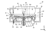
次に、処理ユニット16の概要について、図2および図3を参照しながら説明する。図2は、実施形態に係る処理ユニット16の構成を示す上面図であり、図3は、図2におけるA−A線断面図である。なお、理解の容易のため、図3ではウェハWが搬入された状態を示すとともに、リードスクリュー54の図示を省略している。
<Outline of processing unit>
Next, an overview of the
図2に示すように、処理ユニット16は、筐体20と、基板処理部30と、隔壁部40と、液供給部50とを備える。筐体20は、基板処理部30と、隔壁部40と、液供給部50とを収容する。
As shown in FIG. 2, the
筐体20は、搬送部15と接する位置に搬入出口21を有する。そして、搬送部15の基板搬送装置17で搬送されたウェハWは、かかる搬入出口21から筐体20の内部に搬入される。また、筐体20は、かかる搬入出口21を開閉可能に構成されるシャッター22を有する。
The
図3に示すように、筐体20の天井部には、FFU23が設けられる。FFU23は、筐体20内に供給される清浄化された大気雰囲気のダウンフローを形成する。また、筐体20の底部には、FFU23から供給される大気雰囲気を処理ユニット16の外部へ排気する排気口24が形成される。
As shown in FIG. 3, an
基板処理部30は、ウェハWに所定の液処理を施す。図3に示すように、基板処理部30は、基板保持部31と、支柱部32と、液受けカップ33と、回収カップ34と、排液口35とを有する。基板保持部31は、ウェハWを水平に保持する。かかる基板保持部31は、たとえば、ウェハWの外縁部を側方から保持する。
The
支柱部32は、鉛直方向に延在する部材であり、下方側の基端部が図示しない駆動部によって回転可能に支持される。また、図3には図示していないが、支柱部32は、上方側の先端部において基板保持部31を水平に支持することができる。
The support |
そして、基板処理部30は、駆動部を用いて支柱部32を回転させることによって支柱部32に支持された基板保持部31を回転させる。これにより、基板処理部30は、基板保持部31に保持されたウェハWを回転させる。また、支柱部32は、上下に移動可能に構成されており、基板処理部30の上方に搬入されたウェハWに向かって移動し、ウェハWを受け取ることができる。
Then, the
液受けカップ33は、略円環状であり、下側に凹んだ湾曲形状を有する。液受けカップ33は、基板保持部31の外縁部を取り囲むように配置され、基板保持部31の回転によってウェハWから飛散する処理液L(図4C参照)を捕集する。たとえば、液受けカップ33は、基板保持部31に保持されたウェハWの同一平面より少なくとも上側における基板保持部31の外縁部を囲むように配置される。なお、液受けカップ33は、基板保持部31とともに回転してもよい。
The
回収カップ34は、基板保持部31を取り囲むように配置され、基板保持部31の回転によってウェハWから飛散する処理液Lを捕集する。なお、図3には図示していないが、回収カップ34は、複数の処理液Lをそれぞれ捕集可能なマルチカップであってもよい。
The
かかる回収カップ34の底部には、排液口35が形成されている。そして、液受けカップ33または回収カップ34によって捕集された処理液Lは、かかる排液口35から処理ユニット16の外部へ排出される。
A
隔壁部40は、筐体20の内部において、上述の搬入出口21から基板処理部30までの第1空間A1と、かかる第1空間A1以外の第2空間A2との間を仕切る。また、隔壁部40は、仕切られた第1空間A1内の雰囲気を所定の条件に調整可能に構成される。
The
図3に示すように、隔壁部40は、天板部41と、側壁部42と、隙間埋め部43と、ガス供給部44とを有する。天板部41は、略円板状の形状を有し、基板保持部31に保持されたウェハWと略平行に向かい合って設けられ、ウェハWの上方を覆うように配置される。
As shown in FIG. 3, the
また、天板部41は、筐体20内を上下に移動可能に構成され、ウェハWが搬入出口21から搬入出される際には、ウェハWの搬送路と干渉しない上方に移動する。一方で、天板部41は、ウェハWが基板処理部30で処理される際には、かかるウェハWに近接する下方の位置に移動する。
The
天板部41には、上下に連通する貫通孔41aが形成される。たとえば、図2に示すように、かかる貫通孔41aはスリット状であり、少なくとも基板保持部31に保持されたウェハWの中心部に対向するように形成される。また、貫通孔41aは、後述する処理液ノズル51を挿通可能に形成される。
The
また、図3に示すように、天板部41は、ウェハWに向かって突出する凸部41bを有する。かかる凸部41bは、たとえば略円柱状に突出する。そして、凸部41bの外径は、向かい合うウェハWの外径より大きく、隣接する液受けカップ33の内径より小さい。
As shown in FIG. 3, the
側壁部42は、ウェハWを保持する基板保持部31や液受けカップ33、天板部41などの側方を囲む。側壁部42は、たとえば、図2に示すように、上面視で搬入出口21がある手前側が直線状であり、ウェハWが液処理される奥側がウェハWの形状に沿った半円状の形状を有する。
The
実施形態において、側壁部42は、天板部41と一体で上下に移動可能である。一方で、側壁部42は、天板部41とともに上下に移動する必要はなく、筐体20内で固定されていてもよい。この場合、天板部41は、固定された側壁部42に沿って上下に移動可能に構成されるとよい。
In the embodiment, the
隙間埋め部43は、ウェハWが基板処理部30で処理される際に、第1空間A1における基板処理部30以外の隙間(たとえば、搬入出口21の周辺)を埋める。また、隙間埋め部43は、筐体20内を移動可能に構成され、ウェハWが搬入出口21から搬入出される際には、ウェハWの搬送路と干渉しない位置に移動する。隙間埋め部43は、たとえば、図2に示すように、上面視において内側が円弧状であり、外側が矩形状の略U字形状を有する。
The
ガス供給部44は、第1空間A1に接続され、かかる第1空間A1に雰囲気調整ガスを供給する。たとえば、ガス供給部44における雰囲気調整ガスの吐出ノズルが、搬入出口21と基板処理部30との間の天板部41に設けられる。
The
なお、実施形態における雰囲気調整ガスは、たとえば、窒素ガスやArガスなどの大気雰囲気より酸素濃度が低い不活性ガスや、乾燥ガスなどの大気雰囲気より湿度が低いガスなどである。 Note that the atmosphere adjustment gas in the embodiment is, for example, an inert gas having a lower oxygen concentration than the air atmosphere such as nitrogen gas or Ar gas, or a gas having a lower humidity than the air atmosphere such as a dry gas.
図2に示す液供給部50は、第1空間A1に保持されたウェハWに対して処理液Lを供給する。液供給部50は、処理液ノズル51と、ノズルバス52と、アーム53と、リードスクリュー54とを有し、第2空間A2に配置される。
The
処理液ノズル51は、図示しないバルブおよび流量調整器を介して処理液供給源に接続され、天板部41に形成された貫通孔41aを用いてウェハWに処理液Lを吐出する。
The processing
処理液ノズル51から吐出される処理液Lは、たとえば、酸系処理液やアルカリ系処理液、有機系処理液、リンス液などウェハWの各種液処理に用いられる様々な液体を含む。酸系処理液は、たとえば、DHF(Diluted HydroFluoric acid:希フッ酸)などである。アルカリ系処理液は、たとえばSC1(アンモニア、過酸化水素および水の混合液)などである。有機系処理液は、たとえば、IPA(IsoPropyl Alcohol)などである。リンス液は、たとえば、DIW(DeIonized Water:脱イオン水)などである。
The processing liquid L discharged from the processing
ノズルバス52は、処理液ノズル51を待機位置で待機させるとともに、処理液ノズル51から処理液Lをダミーディスペンスするための容器である。アーム53は、処理液ノズル51を支持する。
The
リードスクリュー54には、らせん溝が形成されている。また、リードスクリュー54は、回動可能に軸支され、図示しない駆動部から駆動力が伝達されることにより、回転軸を軸に所定の回転方向に回転する。
A spiral groove is formed in the
そして、リードスクリュー54を所定の回転方向に回転させることにより、リードスクリュー54のらせん溝に連結されたアーム53が処理液ノズル51とともにリードスクリュー54の回転軸に沿ってスライド移動する。これにより、処理液ノズル51を筐体20内の所定の位置にスライド移動させることができる。
Then, by rotating the
また、アーム53には図示しない昇降機構が備えられている。そして、液供給部50は、かかる昇降機構を動作させることにより、処理液ノズル51を昇降させることができる。
The
このように、液供給部50は、リードスクリュー54および昇降機構を動作させることにより、処理液ノズル51を貫通孔41aの位置に移動させて、かかる貫通孔41aに挿通させることができる。すなわち、アーム53は、処理液ノズル51から貫通孔41aを介して処理液Lを吐出する処理位置と、ウェハWより外方の待機位置との間で処理液ノズル51を移動させる。
Thus, the
また、実施形態では、貫通孔41aがスリット状であり、リードスクリュー54の軸方向と貫通孔41aの延伸方向とが略平行であることから、貫通孔41a内で処理液ノズル51をスキャン移動させることができる。
In the embodiment, the through
なお、図2に示した例では、処理液ノズル51、ノズルバス52およびアーム53が2組設けられた場合について示したが、処理ユニット16に設けられる処理液ノズル51、ノズルバス52およびアーム53は2組に限られず、所定の数設けることができる。
In the example shown in FIG. 2, the case where two sets of the processing
また、図2に示した例では、処理液ノズル51がアーム53に固定されている場合について示したが、処理液ノズル51はアーム53に固定されている場合に限られず、ピックアップノズルなどであってもよい。また、アーム53をスライド移動させる機構はリードスクリュー54に限られず、様々な既知の機構を用いることができる。
In the example shown in FIG. 2, the case where the processing
<液処理の詳細>
つづいて、図4A〜図4Dを参照しながら、実施形態に係る液処理の詳細について説明する。図4A〜図4Dは、実施形態に係る液処理の一工程を示す模式図(1)〜(4)である。
<Details of liquid treatment>
Next, details of the liquid processing according to the embodiment will be described with reference to FIGS. 4A to 4D. Drawing 4A-Drawing 4D are mimetic diagrams (1)-(4) showing one process of liquid processing concerning an embodiment.
図4Aに示すように、処理ユニット16では、ウェハWを基板処理部30に搬入するに先立って、第1空間A1におけるウェハWの搬送路を確保する。具体的には、処理ユニット16は、ウェハWの搬送路から天板部41を上方に退避させるとともに、隙間埋め部43を下方に退避させる。
As shown in FIG. 4A, in the
また、処理ユニット16は、ウェハWを基板処理部30に搬入する前の所定のタイミングから、ガス供給部44を用いて所定の雰囲気調整ガスを第1空間A1に供給する(ステップS1)。これにより、処理ユニット16は、事前に第1空間A1内の雰囲気を雰囲気調整ガスで置換することができる。
Further, the
一方で、処理ユニット16の第2空間A2は、FFU23を用いて清浄化された大気雰囲気である。そして、第1空間A1に供給された雰囲気調整ガスと、第2空間A2に供給された大気雰囲気とは、排気口24で共通に排気される。
On the other hand, the second space A2 of the
次に、処理ユニット16は、シャッター22を移動させて搬入出口21を開放する。そして、基板搬送装置17は、ウェハWを処理ユニット16内に搬入する(ステップS2)。そして、処理ユニット16は、基板保持部31の上方まで搬入されたウェハWを、上方に移動させた支柱部32で受け取ってから下方に移動させて、基板保持部31で保持する(ステップS3)。
Next, the
次に、図4Bに示すように、処理ユニット16は、シャッター22を移動させて搬入出口21を閉じる(ステップS4)。また、処理ユニット16は、天板部41を下方に移動させて、ウェハWに近接させる(ステップS5)。たとえば、かかるステップS5では、天板部41とウェハWとのギャップが1〜4mm程度となる位置に天板部41を近接させる。
Next, as shown in FIG. 4B, the
また、処理ユニット16は、隙間埋め部43を上方に移動させて、第1空間A1における基板処理部30以外の隙間を埋める(ステップS6)。なお、図4Bに示したステップS4〜S6の順番は任意であり、たとえば、ステップS4〜S6はすべて同時に行ってもよい。
In addition, the
実施形態では、かかるステップS4〜S6の間、処理ユニット16は、ガス供給部44を動作させて所定の雰囲気調整ガスを第1空間A1に供給し続ける。これにより、ウェハWが配置された第1空間A1の雰囲気を所定の条件に調整し続けることができる。
In the embodiment, during such steps S4 to S6, the
次に、図4Cに示すように、処理ユニット16は、液供給部50を動作させることにより、処理液ノズル51をウェハW上の所定の位置に移動させて、貫通孔41aに挿通させる(ステップS7)。そして、処理ユニット16は、処理液ノズル51を動作させることにより、ウェハWに所定の処理液Lを供給する(ステップS8)。なお、処理液ノズル51を貫通孔41aに挿通させる動作は、雰囲気調整ガスを供給する前(例えば、ステップS4の前)に行ってもよい。
Next, as shown in FIG. 4C, the
また、かかるステップS8において、処理ユニット16は、ウェハWを回転させてもよいし、停止させてもよい。また、ステップS8では、液供給部50は、所定の動作により処理液ノズル51をウェハW上でスキャンさせてもよい。
In step S8, the
次に、図4Dに示すように、処理ユニット16は、基板処理部30を動作させることにより、ウェハWを回転させる(ステップS9)。これにより、処理液LがウェハWの外周側に移動して、ウェハWが液処理される(ステップS10)。なお、かかる液処理の具体的な例については後述する。
Next, as illustrated in FIG. 4D, the
実施形態では、かかるステップS7〜S10の間、処理ユニット16は、ガス供給部44を動作させて所定の雰囲気調整ガスを第1空間A1に供給し続ける。これにより、液処理されるウェハW周囲の雰囲気を所定の条件に調整し続けることができる。
In the embodiment, during such steps S7 to S10, the
ここで、実施形態では、筐体20内の第2空間A2には大気雰囲気が供給され、隔壁部40で仕切られた第1空間A1に限って雰囲気調整ガスが供給されている。したがって、実施形態によれば、ウェハWを液処理する際における雰囲気調整ガスの使用量を削減することができる。
Here, in the embodiment, an air atmosphere is supplied to the second space A <b> 2 in the
また、実施形態では、天板部41をウェハWに近接させるとともに、隙間埋め部43で第1空間A1の隙間を埋めることにより、第1空間A1を狭小にすることができる。したがって、実施形態によれば、雰囲気調整ガスの使用量をさらに削減することができる。
In the embodiment, the first space A1 can be narrowed by making the
また、実施形態では、液受けカップ33の内径を天板部41の凸部41bの外径より大きくするとよい。これにより、図4Bなどに示すように、液受けカップ33に干渉することなく、天板部41をウェハWに近接させることができる。したがって、実施形態によれば、雰囲気調整ガスの使用量をさらに削減することができる。
In the embodiment, the inner diameter of the
また、実施形態では、図4Cおよび図4Dに示すように、ウェハWを液処理する際に、天板部41とウェハWとの間を処理液Lで満たすとよい。これにより、液処理する際のウェハW上の処理液Lの膜厚を均等にすることができる。したがって、実施形態によれば、ウェハWの液処理を良好な状態で実施することができる。
In the embodiment, as shown in FIGS. 4C and 4D, when the wafer W is subjected to liquid processing, the space between the
また、実施形態では、天板部41とウェハWとの間を処理液Lで満たすことにより、高温処理する際に蒸発した処理液Lが天板部41に付着することを抑制することができる。さらに、実施形態では、天板部41とウェハWとの間を処理液Lで満たすことにより、天板部41に別途追加した加熱手段(たとえば、ヒータなど)で処理液Lを容易に昇温することができる。
Further, in the embodiment, by filling the space between the
なお、実施形態では、天板部41とウェハWとの間を処理液Lで満たした場合でも、ウェハWの回転を比較的低速で開始し、徐々に回転速度を上げることにより、天板部41表面の処理液LをウェハW表面の処理液Lとともに外周側に移動させることができる。これにより、実施形態では、液処理の後、天板部41の表面に処理液Lが残ることを抑制することができる。
In the embodiment, even when the space between the
また、実施形態では、図4Dなどに示すように、天板部41の凸部41bの外径を、ウェハWの外径より大きくするとよい。これにより、液処理の後に凸部41bの外縁部に処理液Lが残った場合でも、かかる残った処理液LがウェハWに付着することを抑制することができる。
In the embodiment, as shown in FIG. 4D and the like, the outer diameter of the
なお、液処理の後に凸部41bの外縁部に処理液Lが残った場合には、かかる外縁部に残った処理液Lを雰囲気調整ガスなどでパージするとよい。
In addition, when the processing liquid L remains on the outer edge portion of the
また、実施形態では、貫通孔41aが、少なくとも基板保持部31に保持されたウェハWの中心部に対向するように形成されるとよい。これにより、処理液ノズル51をウェハWの中心部の上方に配置することができることから、ウェハWの中心部に対して処理液Lを吐出することができる。したがって、実施形態によれば、ウェハWの全面に均等に処理液Lを供給することができる。
In the embodiment, the through
処理ユニット16における処理の続きを説明する。液処理が終わった処理ユニット16は、ウェハWの搬送路から天板部41を上方に退避させるとともに、隙間埋め部43を下方に退避させて、第1空間A1におけるウェハWの搬送路を確保する。
The continuation of the processing in the
そして、シャッター22を移動させて搬入出口21を開放し、基板搬送装置17を用いてウェハWを処理ユニット16から搬出する。最後に、処理ユニット16は、シャッター22を閉じるとともに、ガス供給部44による雰囲気調整ガスの供給を停止する。
Then, the
このように、ウェハWが搬出された第1空間A1への雰囲気調整ガスの供給を停止することにより、雰囲気調整ガスの使用量をさらに削減することができる。 Thus, by stopping the supply of the atmosphere adjustment gas to the first space A1 from which the wafer W has been unloaded, the usage amount of the atmosphere adjustment gas can be further reduced.
また、実施形態では、上述のように、ウェハWが搬入される前にガス供給部44による雰囲気調整ガスの供給を開始して、第1空間A1を事前に雰囲気調整ガスで置換するとよい。これにより、雰囲気が調整された第1空間A1にウェハWを搬入することができる。
In the embodiment, as described above, the supply of the atmosphere adjustment gas by the
また、実施形態では、第1空間A1を雰囲気調整ガスで事前に置換する際に、第1空間A1内で基板保持部31を回転させてもよい。これにより、第1空間A1内に雰囲気調整ガス以外の雰囲気が滞留することを抑制することができることから、効率よく第1空間A1を雰囲気調整ガスで置換することができる。
In the embodiment, the
なお、実施形態では、第1空間A1と第2空間A2との間が貫通孔41aで連通していることから、かかる貫通孔41aを介して第2空間A2の大気雰囲気が第1空間A1に流入する可能性がある。
In the embodiment, since the first space A1 and the second space A2 are communicated with each other through the through
そこで、実施形態では、第1空間A1への大気雰囲気の流入を抑制する流入抑制部45(図5A参照)を設けている。つづいては、かかる流入抑制部45の詳細について、図5A〜図5Cを参照しながら説明する。なお、流入抑制部45による大気雰囲気の流入を抑制する動作は、雰囲気調整ガスの供給中に行われる。
Therefore, in the embodiment, an inflow suppression unit 45 (see FIG. 5A) that suppresses the inflow of the air atmosphere into the first space A1 is provided. Next, the details of the
図5Aは、実施形態に係る流入抑制部45の一例を説明するための模式図であり、天板部41の貫通孔41aが含まれる部位の断面を模式的に示した図である。図5Aに示すように、流入抑制部45は、第1配管部45aと第2配管部45bとを有する。
FIG. 5A is a schematic diagram for explaining an example of the
第1配管部45aおよび第2配管部45bは、貫通孔41aの内壁における互いに向かい合う位置に接続される。第1配管部45aは、雰囲気調整ガスなどを供給する図示しないガス供給機構に接続され、かかるガス供給機構から供給されたガスを貫通孔41a内に吐出する。
The
また、第2配管部45bは、図示しない排気機構に接続され、かかる排気機構により貫通孔41a内の雰囲気を排気する。このように、流入抑制部45は、第1配管部45aから吐出されたガスを向かい合う第2配管部45bで排気することにより、貫通孔41a内にいわゆるガスカーテンを形成することができる。
The
これにより、第2空間A2の大気雰囲気が第1空間A1に流入することを抑制することができる。したがって、実施形態によれば、所定の条件に調整された雰囲気で第1空間A1を良好に維持することができる。なお、図5Aに示した例では、第2配管部45bから吐出されたガスを向かい合う第1配管部45aで排気してもよい。
Thereby, it can suppress that the air atmosphere of 2nd space A2 flows in into 1st space A1. Therefore, according to the embodiment, the first space A1 can be favorably maintained in an atmosphere adjusted to a predetermined condition. In the example shown in FIG. 5A, the gas discharged from the
図5Bは、実施形態に係る流入抑制部45の別の例を説明するための模式図である。図5Bの例では、第1配管部45aおよび第2配管部45bの両方から雰囲気調整ガスなどを吐出している。これによっても、貫通孔41a内にガスカーテンを形成することができる。
FIG. 5B is a schematic diagram for explaining another example of the
したがって、図5Bの例でも、第2空間A2の大気雰囲気が第1空間A1に流入することを抑制することができることから、所定の条件に調整された雰囲気で第1空間A1を良好に維持することができる。 Therefore, in the example of FIG. 5B as well, since the atmospheric atmosphere of the second space A2 can be suppressed from flowing into the first space A1, the first space A1 is favorably maintained in an atmosphere adjusted to a predetermined condition. be able to.
なお、第1配管部45aおよび第2配管部45bの両方から雰囲気調整ガスなどを吐出する場合、図5Bに示すように、第1配管部45aおよび第2配管部45bの吐出方向を斜め上側(すなわち、第2空間A2側)に向けて向かい合うようにするとよい。これにより、第2空間A2の大気雰囲気が第1空間A1に流入することを効果的に抑制することができることから、所定の条件に調整された雰囲気で第1空間A1をさらに良好に維持することができる。
In addition, when discharging atmosphere adjustment gas etc. from both the
図5Cは、実施形態に係る流入抑制部45のさらに別の例を説明するための模式図である。図5Cの例では、第1配管部45aおよび第2配管部45bの両方から排気している。これにより、第2空間A2から貫通孔41a内に流入する大気雰囲気を、第1配管部45aおよび第2配管部45bを用いて外部に排気することができる。
FIG. 5C is a schematic diagram for explaining still another example of the
したがって、図5Cの例でも、第2空間A2の大気雰囲気が第1空間A1に流入することを抑制することができることから、所定の条件に調整された雰囲気で第1空間A1を良好に維持することができる。 Therefore, even in the example of FIG. 5C, since the atmospheric atmosphere of the second space A2 can be suppressed from flowing into the first space A1, the first space A1 is favorably maintained in an atmosphere adjusted to a predetermined condition. be able to.
なお、実施形態では、処理液ノズル51を貫通孔41aに挿通させた状態で処理液LをウェハWに供給した例について示している。一方で、処理液ノズル51を貫通孔41aに挿通させることなく、貫通孔41aの上方に配置した処理液ノズル51から、処理液Lを貫通孔41a内に通流させてウェハWに供給してもよい。
In the embodiment, an example is shown in which the processing liquid L is supplied to the wafer W in a state where the processing
一方で、処理液ノズル51を貫通孔41aに挿通させた状態で処理液LをウェハWに供給することにより、ここまで説明した流入抑制部45より第1空間A1側で処理液Lを吐出することができる。すなわち、貫通孔41a内に処理液Lを通流させる場合よりも、流入抑制部45を十分に機能させることができる。
On the other hand, by supplying the processing liquid L to the wafer W in a state where the processing
したがって、実施形態によれば、処理液ノズル51を貫通孔41aに挿通させた状態で処理液LをウェハWに供給することにより、所定の条件に調整された雰囲気で第1空間A1を良好に維持することができる。
Therefore, according to the embodiment, by supplying the processing liquid L to the wafer W in a state where the processing
<変形例>
つづいて、図6〜図9Cを参照しながら、実施形態にかかる処理ユニット16の各種変形例について説明する。図6は、実施形態の変形例1に係る処理ユニット16の構成を示す上面図である。
<Modification>
Subsequently, various modifications of the
図6に示す変形例1では、貫通孔41aがスリット状ではなく、挿通される処理液ノズル51と同様の形状(たとえば、略円状)である。かかる変形例1でも、基板保持部31に保持されたウェハWの中心部に対向するように貫通孔41aを配置することにより、ウェハWの全面に均等に処理液Lを供給することができる。
In the first modification shown in FIG. 6, the through
図7は、実施形態の変形例2に係る処理ユニット16の構成を示す上面図である。図7に示す変形例2では、貫通孔41aが直線状のスリットではなく、円弧状のスリットである。
FIG. 7 is a top view illustrating a configuration of the
かかる変形例2では、処理液ノズル51が貫通孔41aに沿って回動するように液供給部50を構成することにより、実施形態と同様に貫通孔41a内で処理液ノズル51をスキャン移動させることができる。
In the second modification, by configuring the
なお、変形例2でも、少なくともウェハWの中心部に対向するように貫通孔41aを配置することにより、ウェハWの全面に均等に処理液Lを供給することができる。
In the second modification as well, the processing liquid L can be evenly supplied to the entire surface of the wafer W by disposing the through
次に、処理ユニット16の変形例3について、図8A〜図8Dを用いて説明する。図8A〜図8Dは、実施形態の変形例3に係る処理ユニット16による液処理の一工程を示す模式図(1)〜(4)である。なお、図8A〜図8Dでは、処理ユニット16の模式的な斜視図を示している。
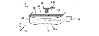
Next,
図8Aに示すように、変形例3の処理ユニット16では、天板部41にスリット状の貫通孔41aがウェハWの中心部から外縁部に向かって直線状に形成されている。また、スキャン天板55が、貫通孔41aを覆うとともに、ウェハWの一方の外縁部から他方の外縁部まで延びるように配置されている。かかるスキャン天板55は、貫通孔41aに沿って移動可能に構成される。
As shown in FIG. 8A, in the
さらに、変形例3の処理ユニット16は、複数の処理液ノズル51がピックアップノズルとして設けられている。そして、かかる複数の処理液ノズル51を挿通可能な複数の貫通孔55aがスキャン天板55に形成されている。
Further, the
この変形例3の処理ユニット16では、まず、処理液ノズル51から処理液Lのダミーディスペンスを行う(ステップS21)。
In the
次に、図8Bに示すように、処理ユニット16は、図示しない搬送部で処理液ノズル51をピックアップし、かかる処理液ノズル51をウェハW中央部の上方に搬送する(ステップS22)。なお、かかるステップS22の際に、スキャン天板55の貫通孔55aは、ウェハW中央部の上方に配置される。
Next, as shown in FIG. 8B, the
次に、図8Cに示すように、処理ユニット16は、スキャン天板55の貫通孔55aを介して、処理液ノズル51を天板部41の貫通孔41aに挿通させる(ステップS23)。そして、処理ユニット16は、貫通孔41aに挿通された処理液ノズル51から、処理液LをウェハWに供給する(ステップS24)。
Next, as illustrated in FIG. 8C, the
次に、図8Dに示すように、処理ユニット16は、処理液ノズル51をスキャン天板55と同期させて移動させながら、処理液Lが吐出されている処理液ノズル51をウェハW上でスキャンさせる(ステップS25)。なお、ステップS25では、処理液ノズル51をピックアップした搬送部で処理液ノズル51を移動させてもよいし、スキャン天板55で処理液ノズル51を移動させてもよい。
Next, as illustrated in FIG. 8D, the
ここまで説明したように、変形例3では、処理液ノズル51と同期して移動するスキャン天板55で貫通孔41aを覆うことにより、第2空間A2の大気雰囲気が貫通孔41aを介して第1空間A1に流入することを抑制することができる。したがって、変形例3によれば、所定の条件に調整された雰囲気で第1空間A1を良好に維持することができる。
As described so far, in
次に、処理ユニット16の変形例4について、図9A〜図9Cを用いて説明する。図9A〜図9Cは、実施形態の変形例4に係る処理ユニット16による液処理の一工程を示す模式図(1)〜(3)である。なお、図9A〜図9Cでは、処理ユニット16の模式的な上面図を示している。
Next, Modification 4 of the
変形例4では、1つの処理ユニット16に複数(たとえば、2つ)の基板処理部30が設けられ、1つの処理ユニット16で複数のウェハWをまとめて液処理することができる。そして、変形例4の天板部41は、複数の基板処理部30をすべて覆うように配置されるとともに、基板処理部30の上方で回転可能に構成される。
In the fourth modification, a plurality of (for example, two)
また、変形例4では、天板部41に処理液ノズル51が設けられ、天板部41などで仕切られた第1空間A1内にノズルバス52が設けられる。なお、図9Aの例では、3本の処理液ノズル51と1つのノズルバス52とのセットが2組設けられた例について示している。
Moreover, in the modification 4, the process
かかる変形例4の処理ユニット16は、まず、図9Aに示すように、ノズルバス52の上方に配置された処理液ノズル51から処理液Lのダミーディスペンスを行う。次に、図9Bに示すように、処理ユニット16は、天板部41を回転させて、処理液ノズル51をウェハWの上方に移動させる。
First, the
そして、処理ユニット16は、基板処理部30でウェハWを回転させながら、処理液ノズル51でウェハWに処理液Lを供給する。
Then, the
さらに、図9Cに示すように、処理ユニット16は、処理液ノズル51で処理液Lを供給しながら、天板部41をさらに回転させて、処理液ノズル51をウェハWの上方でスキャンする。
Further, as illustrated in FIG. 9C, the
ここまで説明したように、変形例4では、天板部41などで仕切られ、雰囲気調整ガスで雰囲気が調整された第1空間A1内の複数のウェハWに処理液Lを供給することができる。
As described so far, in the fourth modification, the processing liquid L can be supplied to the plurality of wafers W in the first space A1 that is partitioned by the
また、変形例4では、図9Aなどに示したように、処理液ノズル51を基板処理部30の数に対応する分用意するとよい。これにより、変形例4では、処理ユニット16に収容された複数のウェハWに対して同時に液処理を行うことができる。
In Modification 4, as shown in FIG. 9A and the like, it is preferable to prepare the processing
なお、変形例4では、天板部41を回転させる際に、処理液ノズル51が少なくともウェハWの中心部を通過するように配置されるとよい。これにより、ウェハWの全面に均等に処理液Lを供給することができる。
In the fourth modification, when the
実施形態に係る基板処理装置(処理ユニット16)は、基板保持部31と、天板部41と、ガス供給部44と、処理液ノズル51と、アーム53とを備える。基板保持部31は、基板(ウェハW)を保持する。天板部41は、基板保持部31に保持された基板(ウェハW)に向かい合って設けられ、少なくとも基板(ウェハW)の中心に対向する位置に貫通孔41aが形成される。ガス供給部44は、基板保持部31と天板部41との間の空間(第1空間A1)に雰囲気を調整する雰囲気調整ガスを供給する。処理液ノズル51は、基板(ウェハW)を処理する処理液Lを基板(ウェハW)に吐出する。アーム53は、処理液ノズル51を保持し、処理液ノズル51から貫通孔41aを介して処理液Lを吐出する処理位置と基板(ウェハW)より外方の待機位置との間で移動させる。これにより、ウェハWを液処理する際における雰囲気調整ガスの使用量を削減することができる。
The substrate processing apparatus (processing unit 16) according to the embodiment includes a
また、実施形態に係る基板処理装置(処理ユニット16)において、天板部41は、基板(ウェハW)と天板部41との間の空間(第1空間A1)に貫通孔41aを経由して雰囲気調整ガスとは異なるガスが流入することを抑制する流入抑制部45を有する。これにより、所定の条件に調整された雰囲気で第1空間A1を良好に維持することができる。
In the substrate processing apparatus (processing unit 16) according to the embodiment, the
また、実施形態に係る基板処理装置(処理ユニット16)において、貫通孔41aは、スリット状である。これにより、貫通孔41a内で処理液ノズル51をスキャン移動させることができる。
In the substrate processing apparatus (processing unit 16) according to the embodiment, the through
また、変形例3に係る基板処理装置(処理ユニット16)は、スリット状の貫通孔41aを覆うように配置され、処理液ノズル51と同期して基板(ウェハW)上でスキャンされるスキャン天板55をさらに備える。これにより、所定の条件に調整された雰囲気で第1空間A1を良好に維持することができる。
Further, the substrate processing apparatus (processing unit 16) according to
また、変形例4に係る基板処理装置(処理ユニット16)は、基板保持部31が複数並んで設けられる。そして、天板部41は、複数の基板保持部31を覆うように配置され、複数の基板保持部31上で回動可能である。これにより、天板部41などで仕切られ、雰囲気調整ガスで雰囲気が調整された第1空間A1内の複数のウェハWに処理液Lを供給することができる。
Further, the substrate processing apparatus (processing unit 16) according to Modification 4 is provided with a plurality of
また、実施形態に係る基板処理装置(処理ユニット16)において、天板部41は、基板(ウェハW)に向かって突出する凸部41bを有し、凸部41bの外径は、基板(ウェハW)の外径より大きい。これにより、液処理の後に凸部41bの外縁部に処理液Lが残った場合でも、かかる残った処理液LがウェハWに付着することを抑制することができる。
In the substrate processing apparatus (processing unit 16) according to the embodiment, the
また、実施形態に係る基板処理装置(処理ユニット16)は、基板保持部31の外縁部を取り囲むように配置され、液処理された処理液Lを受ける液受けカップ33をさらに備える。そして、液受けカップ33の内径は、凸部41bの外径より大きい。これにより、液受けカップ33に干渉することなく、天板部41をウェハWに近接させることができる。
The substrate processing apparatus (processing unit 16) according to the embodiment further includes a
<液処理の詳細>
つづいて、図10および図11を参照しながら、実施形態に係る液処理の詳細について説明する。図10は、実施形態に係る液処理全体の処理手順を示すフローチャートである。
<Details of liquid treatment>
Next, details of the liquid processing according to the embodiment will be described with reference to FIGS. 10 and 11. FIG. 10 is a flowchart showing a processing procedure of the entire liquid processing according to the embodiment.
なお、図10および図11に示す液処理は、実施形態に係る記憶媒体から記憶部19にインストールされたプログラムを制御部18が読み出すとともに、読み出した命令に基づいて、制御部18が搬送部12や搬送部15、処理ユニット16などを制御することにより実行される。
10 and FIG. 11, the control unit 18 reads out the program installed in the storage unit 19 from the storage medium according to the embodiment, and the control unit 18 controls the
まず、制御部18は、処理ユニット16のガス供給部44を制御して、隔壁部40で仕切られた第1空間A1に雰囲気調整ガスを供給する(ステップS101)。つづいて、制御部18は、基板搬送装置13および基板搬送装置17を制御して、キャリアCから、基板搬送装置13と、受渡部14と、基板搬送装置17とを経由して、ウェハWを処理ユニット16の内部に搬入する(ステップS102)。
First, the control unit 18 controls the
次に、制御部18は、処理ユニット16の基板処理部30を制御して、基板保持部31でウェハWを保持する(ステップS103)。かかるステップS103は、たとえば、基板保持部31の上方まで搬入されたウェハWを、上方に移動させた支柱部32で受け取ってから下方に移動させて、基板保持部31で保持することにより行われる。
Next, the control unit 18 controls the
次に、制御部18は、処理ユニット16の隔壁部40を制御して、天板部41をウェハWに近接させる(ステップS104)。また、ステップS104の処理と平行して、制御部18は、隔壁部40を制御して、第1空間A1の隙間を隙間埋め部43で埋める(ステップS105)。
Next, the control unit 18 controls the
次に、制御部18は、処理ユニット16の液供給部50を制御して、処理液ノズル51を天板部41の貫通孔41aに挿通する(ステップS106)。そして、制御部18は、液供給部50を制御して、処理液ノズル51から処理液LをウェハWに供給する(ステップS107)。
Next, the control unit 18 controls the
次に、制御部18は、基板処理部30を制御して、ウェハWを液処理する(ステップS108)。かかるステップS108は、たとえば、基板保持部31を回転させることによりウェハWを回転させて、ウェハWに供給された処理液Lを外周側に移動させることにより行われる。また、上述のステップS107およびS108は、天板部41とウェハWとの間を処理液Lで満たすように行われる。
Next, the control unit 18 controls the
次に、制御部18は、隔壁部40を制御して、第1空間A1におけるウェハWの搬送路を確保する(ステップS109)。かかるステップS109は、たとえば、ウェハWの搬送路から天板部41を上方に退避させるとともに、隙間埋め部43を下方に退避させることにより行われる。
Next, the control unit 18 controls the
次に、制御部18は、基板処理部30、基板搬送装置17および基板搬送装置13を制御して、処理ユニット16の内部から基板搬送装置17と、受渡部14と、基板搬送装置13とを経由して、キャリアCにウェハWを搬出する(ステップS110)。
Next, the control unit 18 controls the
最後に、制御部18は、ガス供給部44を制御して、隔壁部40で仕切られた第1空間A1への雰囲気調整ガスの供給を停止して(ステップS111)、処理を完了する。
Finally, the control unit 18 controls the
図11は、実施形態に係る液処理(上述のステップS108)の詳細な処理手順を示すフローチャートである。 FIG. 11 is a flowchart showing a detailed processing procedure of the liquid processing (the above-described step S108) according to the embodiment.
実施形態の液処理は、まず所定の第1処理液で第1液処理を行う(ステップS201)。かかる第1液処理は、たとえば、DHFなどの酸系処理液やSC1などのアルカリ系処理液といった第1処理液を処理液ノズル51からウェハWに供給することにより行われる。
In the liquid treatment of the embodiment, first, a first liquid treatment is performed with a predetermined first treatment liquid (step S201). The first liquid processing is performed by supplying a first processing liquid such as an acid processing liquid such as DHF or an alkaline processing liquid such as SC1 from the processing
次に、所定のリンス液でリンス処理を行う(ステップS202)。かかるリンス処理は、たとえば、DIWなどのリンス液を処理液ノズル51からウェハWに供給することにより行われる。なお、かかるリンス処理により、天板部41に付着した第1処理液も表面から除去することができる。
Next, a rinsing process is performed with a predetermined rinsing solution (step S202). The rinsing process is performed, for example, by supplying a rinsing liquid such as DIW from the processing
次に、所定の第2処理液で第2液処理を行う(ステップS203)。かかる第2液処理は、たとえば、DHFなどの酸系処理液やSC1などのアルカリ系処理液といった第2処理液を処理液ノズル51からウェハWに供給することにより行われる。
Next, a second liquid treatment is performed with a predetermined second treatment liquid (step S203). Such second liquid processing is performed, for example, by supplying a second processing liquid such as an acid processing liquid such as DHF or an alkaline processing liquid such as SC1 from the processing
次に、所定のリンス液でリンス処理を行う(ステップS204)。かかるリンス処理は、ステップS202と同様の処理である。なお、かかるリンス処理により、天板部41に付着した第2処理液も表面から除去することができる。
Next, a rinsing process is performed with a predetermined rinsing solution (step S204). Such a rinsing process is the same process as step S202. In addition, the 2nd process liquid adhering to the top-
次に、処理液ノズル51を用いて、ウェハWにIPAを供給する(ステップS205)。最後に、IPAが供給されたウェハWを回転させることにより、ウェハWをスピン乾燥して(ステップS206)、処理を完了する。 Next, IPA is supplied to the wafer W using the processing liquid nozzle 51 (step S205). Finally, the wafer W supplied with IPA is rotated to spin dry the wafer W (step S206), thereby completing the process.
実施形態に係る基板処理方法は、雰囲気調整ガスを供給する工程と、基板保持部31で基板を保持する工程と、液処理する工程と、を含む。雰囲気調整ガスを供給する工程は、基板(ウェハW)を保持する基板保持部31と基板保持部31と向かい合って設けられる天板部41との間の空間(第1空間A1)に雰囲気を調整する雰囲気調整ガスを供給する。液処理する工程は、天板部41に形成された貫通孔41aを用いて基板(ウェハW)に処理液Lを供給して液処理する。これにより、ウェハWを液処理する際における雰囲気調整ガスの使用量を削減することができる。
The substrate processing method according to the embodiment includes a step of supplying an atmosphere adjustment gas, a step of holding the substrate by the
また、実施形態に係る基板処理方法は、処理液Lを吐出する処理液ノズル51を貫通孔41aに挿通する工程をさらに含む。これにより、所定の条件に調整された雰囲気で第1空間A1を良好に維持することができる。
The substrate processing method according to the embodiment further includes a step of inserting the processing
また、実施形態に係る基板処理方法は、基板保持部31に保持された基板(ウェハW)に天板部41を近接させる工程をさらに含む。これにより、第1空間A1を狭小にすることができることから、雰囲気調整ガスの使用量をさらに削減することができる。
The substrate processing method according to the embodiment further includes a step of bringing the
また、実施形態に係る基板処理方法において、液処理する工程は、天板部41と基板(ウェハW)との間を処理液Lで満たす。これにより、ウェハWの液処理を良好な状態で実施することができる。
Further, in the substrate processing method according to the embodiment, in the liquid processing step, the space between the
また、実施形態に係る記憶媒体は、上記に記載の基板処理方法をコンピュータに実行させる、プログラムを記憶する。これにより、ウェハWを液処理する際における雰囲気調整ガスの使用量を削減することができる。 The storage medium according to the embodiment stores a program that causes a computer to execute the substrate processing method described above. Thereby, the usage-amount of the atmosphere adjustment gas at the time of liquid-processing the wafer W can be reduced.
以上、本開示の各実施形態について説明したが、本開示は上記実施形態に限定されるものではなく、その趣旨を逸脱しない限りにおいて種々の変更が可能である。たとえば、上述の実施形態では、天板部41とウェハWとの間を処理液Lで満たした場合について説明したが、天板部41とウェハWの間に雰囲気調整ガスを供給しておけば、必ずしも天板部41とウェハWとの間を処理液Lで満たす必要はない。また、雰囲気調整ガスの供給量を処理中に変えてもよい。
As mentioned above, although each embodiment of this indication was described, this indication is not limited to the above-mentioned embodiment, and various changes are possible unless it deviates from the meaning. For example, in the above-described embodiment, the case where the space between the
今回開示された実施形態は全ての点で例示であって制限的なものではないと考えられるべきである。実に、上記した実施形態は多様な形態で具現され得る。また、上記の実施形態は、添付の特許請求の範囲及びその趣旨を逸脱することなく、様々な形態で省略、置換、変更されてもよい。 It should be thought that embodiment disclosed this time is an illustration and restrictive at no points. Indeed, the above-described embodiment can be embodied in various forms. The above embodiments may be omitted, replaced, and modified in various forms without departing from the scope and spirit of the appended claims.
W ウェハ(基板の一例)
L 処理液
1 基板処理システム
16 処理ユニット(基板処理装置の一例)
17 基板搬送装置
20 筐体
21 搬入出口
30 基板処理部
31 基板保持部
32 支柱部
33 液受けカップ
34 回収カップ
40 隔壁部
41 天板部
41a 貫通孔
41b 凸部
42 側壁部
43 隙間埋め部
44 ガス供給部
45 流入抑制部
50 液供給部
51 処理液ノズル
53 アーム
55 スキャン天板
A1 第1空間
A2 第2空間
W wafer (example of substrate)
L processing liquid 1
DESCRIPTION OF
Claims (12)
前記基板保持部に保持された前記基板に向かい合って設けられ、少なくとも前記基板の中心に対向する位置に貫通孔が形成される天板部と、
前記基板保持部と前記天板部との間の空間に雰囲気を調整する雰囲気調整ガスを供給するガス供給部と、
前記基板を処理する処理液を前記基板に吐出する処理液ノズルと、
前記処理液ノズルを保持し、前記処理液ノズルから前記貫通孔を介して前記処理液を吐出する処理位置と前記基板より外方の待機位置との間で移動させるアームと、
を備える基板処理装置。 A substrate holder for holding the substrate;
A top plate portion provided facing the substrate held by the substrate holding portion and having a through hole formed at a position facing at least the center of the substrate;
A gas supply unit for supplying an atmosphere adjustment gas for adjusting an atmosphere in a space between the substrate holding unit and the top plate unit;
A processing liquid nozzle for discharging a processing liquid for processing the substrate onto the substrate;
An arm that holds the processing liquid nozzle and moves the processing liquid from a processing position that discharges the processing liquid from the processing liquid nozzle through the through-hole and a standby position outside the substrate;
A substrate processing apparatus comprising:
前記天板部は、複数の前記基板保持部を覆うように配置され、複数の前記基板保持部上で回動可能である請求項1〜4のいずれか一つに記載の基板処理装置。 A plurality of the substrate holding portions are provided side by side,
The substrate processing apparatus according to claim 1, wherein the top plate portion is disposed so as to cover the plurality of substrate holding portions and is rotatable on the plurality of substrate holding portions.
前記凸部の外径は、前記基板の外径より大きい請求項1〜5のいずれか一つに記載の基板処理装置。 The top plate portion has a convex portion protruding toward the substrate,
The substrate processing apparatus according to claim 1, wherein an outer diameter of the convex portion is larger than an outer diameter of the substrate.
前記液受けカップの内径は、前記凸部の外径より大きい請求項6に記載の基板処理装置。 A liquid receiving cup that is disposed so as to surround an outer edge portion of the substrate holding unit and receives the processing liquid subjected to liquid processing;
The substrate processing apparatus according to claim 6, wherein an inner diameter of the liquid receiving cup is larger than an outer diameter of the convex portion.
前記基板保持部で前記基板を保持する工程と、
前記天板部に形成された貫通孔を用いて前記基板に処理液を供給して液処理する工程と、
を含む基板処理方法。 Supplying an atmosphere adjustment gas for adjusting the atmosphere in a space between a substrate holding part for holding a substrate and a top plate part provided facing the substrate holding part;
Holding the substrate by the substrate holding unit;
A step of supplying a processing liquid to the substrate using a through-hole formed in the top plate portion to perform a liquid processing;
A substrate processing method.
Priority Applications (5)
| Application Number | Priority Date | Filing Date | Title |
|---|---|---|---|
| JP2018093939A JP7090468B2 (en) | 2018-05-15 | 2018-05-15 | Board processing equipment and board processing method |
| TW108115494A TWI791109B (en) | 2018-05-15 | 2019-05-06 | Substrate processing device and substrate processing method |
| KR1020190054155A KR20190130963A (en) | 2018-05-15 | 2019-05-09 | Substrate processing apparatus and substrate processing method |
| US16/407,245 US10892176B2 (en) | 2018-05-15 | 2019-05-09 | Substrate processing apparatus having top plate with through hole and substrate processing method |
| CN201910392650.8A CN110491799B (en) | 2018-05-15 | 2019-05-13 | Substrate processing apparatus and substrate processing method |
Applications Claiming Priority (1)
| Application Number | Priority Date | Filing Date | Title |
|---|---|---|---|
| JP2018093939A JP7090468B2 (en) | 2018-05-15 | 2018-05-15 | Board processing equipment and board processing method |
Publications (2)
| Publication Number | Publication Date |
|---|---|
| JP2019201075A true JP2019201075A (en) | 2019-11-21 |
| JP7090468B2 JP7090468B2 (en) | 2022-06-24 |
Family
ID=68532491
Family Applications (1)
| Application Number | Title | Priority Date | Filing Date |
|---|---|---|---|
| JP2018093939A Active JP7090468B2 (en) | 2018-05-15 | 2018-05-15 | Board processing equipment and board processing method |
Country Status (5)
| Country | Link |
|---|---|
| US (1) | US10892176B2 (en) |
| JP (1) | JP7090468B2 (en) |
| KR (1) | KR20190130963A (en) |
| CN (1) | CN110491799B (en) |
| TW (1) | TWI791109B (en) |
Cited By (1)
| Publication number | Priority date | Publication date | Assignee | Title |
|---|---|---|---|---|
| US11373883B2 (en) * | 2018-06-29 | 2022-06-28 | Tokyo Electron Limited | Substrate processing apparatus, substrate processing system and substrate processing method |
Citations (8)
| Publication number | Priority date | Publication date | Assignee | Title |
|---|---|---|---|---|
| JP2000012458A (en) * | 1998-06-11 | 2000-01-14 | Samsung Electron Co Ltd | Semiconductor device manufacturing equipment |
| JP2001176765A (en) * | 1999-12-20 | 2001-06-29 | Tokyo Electron Ltd | Film-forming device |
| JP2002368066A (en) * | 2001-06-06 | 2002-12-20 | Tokyo Electron Ltd | Processing device |
| JP2008047629A (en) * | 2006-08-11 | 2008-02-28 | Dainippon Screen Mfg Co Ltd | Device and method for processing substrate |
| JP2012204451A (en) * | 2011-03-24 | 2012-10-22 | Dainippon Screen Mfg Co Ltd | Substrate processing device |
| JP2013030613A (en) * | 2011-07-28 | 2013-02-07 | Dainippon Screen Mfg Co Ltd | Substrate processing apparatus and substrate processing method |
| JP2015162557A (en) * | 2014-02-27 | 2015-09-07 | 株式会社Screenホールディングス | substrate processing apparatus and substrate processing method |
| US20150343484A1 (en) * | 2014-05-28 | 2015-12-03 | Spintrac Systems, Inc. | Removable spin chamber with vacuum attachment |
Family Cites Families (24)
| Publication number | Priority date | Publication date | Assignee | Title |
|---|---|---|---|---|
| US6676757B2 (en) * | 1999-12-17 | 2004-01-13 | Tokyo Electron Limited | Coating film forming apparatus and coating unit |
| JP2001319845A (en) | 2000-05-02 | 2001-11-16 | Tokyo Electron Ltd | Coating developing system |
| US6811613B2 (en) * | 2001-11-26 | 2004-11-02 | Tokyo Electron Limited | Coating film forming apparatus |
| JP4565433B2 (en) * | 2001-11-27 | 2010-10-20 | 東京エレクトロン株式会社 | Liquid processing apparatus and liquid processing method |
| JP2004006672A (en) * | 2002-04-19 | 2004-01-08 | Dainippon Screen Mfg Co Ltd | Substrate processing method and apparatus |
| JP4112923B2 (en) * | 2002-07-22 | 2008-07-02 | 芝浦メカトロニクス株式会社 | Substrate processing apparatus and processing method |
| JP3824567B2 (en) * | 2002-09-30 | 2006-09-20 | 株式会社荏原製作所 | Substrate processing equipment |
| JP4865208B2 (en) * | 2004-11-12 | 2012-02-01 | シャープ株式会社 | Atmospheric pressure plasma processing equipment |
| US7914626B2 (en) * | 2005-11-24 | 2011-03-29 | Tokyo Electron Limited | Liquid processing method and liquid processing apparatus |
| JP2007157898A (en) * | 2005-12-02 | 2007-06-21 | Tokyo Electron Ltd | Substrate cleaning method, substrate cleaning device, control program, and computer readable storage medium |
| JP4760516B2 (en) * | 2005-12-15 | 2011-08-31 | 東京エレクトロン株式会社 | Coating apparatus and coating method |
| JP4762098B2 (en) * | 2006-09-28 | 2011-08-31 | 大日本スクリーン製造株式会社 | Substrate processing apparatus and substrate processing method |
| JP5067432B2 (en) * | 2010-02-15 | 2012-11-07 | 東京エレクトロン株式会社 | Coating, developing device, developing method, and storage medium |
| JP5789546B2 (en) * | 2011-04-26 | 2015-10-07 | 東京エレクトロン株式会社 | Coating processing apparatus, coating and developing processing system, coating processing method, and recording medium recording a program for executing the coating processing method |
| JP2013062361A (en) * | 2011-09-13 | 2013-04-04 | Tokyo Electron Ltd | Heat treatment apparatus, temperature control system, heat treatment method, temperature control method, and record medium recording program for executing heat treatment method or temperature control method |
| JP5829092B2 (en) * | 2011-10-13 | 2015-12-09 | 東京エレクトロン株式会社 | Liquid processing apparatus and liquid processing method |
| JP5666414B2 (en) * | 2011-10-27 | 2015-02-12 | 東京エレクトロン株式会社 | Liquid processing apparatus, liquid processing method, and storage medium |
| US8703403B2 (en) * | 2011-12-22 | 2014-04-22 | Taiwan Semiconductor Manufacturing Company, Ltd. | Method and apparatus for drying a wafer |
| JP6090837B2 (en) * | 2012-06-13 | 2017-03-08 | 株式会社Screenホールディングス | Substrate processing apparatus and substrate processing method |
| KR101512560B1 (en) * | 2012-08-31 | 2015-04-15 | 가부시키가이샤 스크린 홀딩스 | Substrate processing apparatus |
| JP2014204018A (en) * | 2013-04-08 | 2014-10-27 | シンフォニアテクノロジー株式会社 | Cooling unit of workpiece |
| JP6032189B2 (en) * | 2013-12-03 | 2016-11-24 | 東京エレクトロン株式会社 | Coating film forming apparatus, coating film forming method, and storage medium |
| EP3112018A1 (en) * | 2015-07-02 | 2017-01-04 | Centrillion Technology Holdings Corporation | Systems and methods to dispense and mix reagents |
| JP6670674B2 (en) * | 2016-05-18 | 2020-03-25 | 株式会社Screenホールディングス | Substrate processing apparatus and substrate processing method |
-
2018
- 2018-05-15 JP JP2018093939A patent/JP7090468B2/en active Active
-
2019
- 2019-05-06 TW TW108115494A patent/TWI791109B/en active
- 2019-05-09 KR KR1020190054155A patent/KR20190130963A/en active IP Right Grant
- 2019-05-09 US US16/407,245 patent/US10892176B2/en active Active
- 2019-05-13 CN CN201910392650.8A patent/CN110491799B/en active Active
Patent Citations (8)
| Publication number | Priority date | Publication date | Assignee | Title |
|---|---|---|---|---|
| JP2000012458A (en) * | 1998-06-11 | 2000-01-14 | Samsung Electron Co Ltd | Semiconductor device manufacturing equipment |
| JP2001176765A (en) * | 1999-12-20 | 2001-06-29 | Tokyo Electron Ltd | Film-forming device |
| JP2002368066A (en) * | 2001-06-06 | 2002-12-20 | Tokyo Electron Ltd | Processing device |
| JP2008047629A (en) * | 2006-08-11 | 2008-02-28 | Dainippon Screen Mfg Co Ltd | Device and method for processing substrate |
| JP2012204451A (en) * | 2011-03-24 | 2012-10-22 | Dainippon Screen Mfg Co Ltd | Substrate processing device |
| JP2013030613A (en) * | 2011-07-28 | 2013-02-07 | Dainippon Screen Mfg Co Ltd | Substrate processing apparatus and substrate processing method |
| JP2015162557A (en) * | 2014-02-27 | 2015-09-07 | 株式会社Screenホールディングス | substrate processing apparatus and substrate processing method |
| US20150343484A1 (en) * | 2014-05-28 | 2015-12-03 | Spintrac Systems, Inc. | Removable spin chamber with vacuum attachment |
Cited By (1)
| Publication number | Priority date | Publication date | Assignee | Title |
|---|---|---|---|---|
| US11373883B2 (en) * | 2018-06-29 | 2022-06-28 | Tokyo Electron Limited | Substrate processing apparatus, substrate processing system and substrate processing method |
Also Published As
| Publication number | Publication date |
|---|---|
| US10892176B2 (en) | 2021-01-12 |
| US20190355593A1 (en) | 2019-11-21 |
| TW201947689A (en) | 2019-12-16 |
| CN110491799B (en) | 2024-04-02 |
| TWI791109B (en) | 2023-02-01 |
| CN110491799A (en) | 2019-11-22 |
| KR20190130963A (en) | 2019-11-25 |
| JP7090468B2 (en) | 2022-06-24 |
Similar Documents
| Publication | Publication Date | Title |
|---|---|---|
| US9305767B2 (en) | Liquid processing apparatus, liquid processing method and storage medium | |
| JP6425639B2 (en) | Substrate processing system | |
| CN107154371B (en) | Liquid processing method, substrate processing apparatus, and storage medium | |
| KR102294642B1 (en) | Liquid processing apparatus | |
| US20200168482A1 (en) | Substrate processing apparatus and substrate processing method | |
| JP2019201075A (en) | Substrate processing apparatus and substrate processing method | |
| JP7213624B2 (en) | SUBSTRATE PROCESSING APPARATUS, SUBSTRATE PROCESSING SYSTEM AND SUBSTRATE PROCESSING METHOD | |
| US11373883B2 (en) | Substrate processing apparatus, substrate processing system and substrate processing method | |
| JP4688533B2 (en) | Substrate processing equipment | |
| JP6917807B2 (en) | Substrate processing method | |
| JP7337175B2 (en) | SUBSTRATE PROCESSING APPARATUS AND SUBSTRATE PROCESSING METHOD | |
| JP5726637B2 (en) | Liquid processing apparatus and liquid processing method | |
| JP5726636B2 (en) | Liquid processing apparatus and liquid processing method | |
| JP7080331B2 (en) | Board processing method and board processing equipment | |
| WO2022196384A1 (en) | Substrate treatment method and substrate treatment device | |
| JP7138493B2 (en) | Substrate liquid processing method, storage medium and substrate liquid processing apparatus | |
| JPWO2019012978A1 (en) | Substrate transfer device and substrate transfer method | |
| CN115332109A (en) | Substrate processing apparatus and substrate processing method |
Legal Events
| Date | Code | Title | Description |
|---|---|---|---|
| A621 | Written request for application examination |
Free format text: JAPANESE INTERMEDIATE CODE: A621 Effective date: 20210312 |
|
| A977 | Report on retrieval |
Free format text: JAPANESE INTERMEDIATE CODE: A971007 Effective date: 20220113 |
|
| A131 | Notification of reasons for refusal |
Free format text: JAPANESE INTERMEDIATE CODE: A131 Effective date: 20220118 |
|
| A521 | Request for written amendment filed |
Free format text: JAPANESE INTERMEDIATE CODE: A523 Effective date: 20220225 |
|
| TRDD | Decision of grant or rejection written | ||
| A01 | Written decision to grant a patent or to grant a registration (utility model) |
Free format text: JAPANESE INTERMEDIATE CODE: A01 Effective date: 20220517 |
|
| A61 | First payment of annual fees (during grant procedure) |
Free format text: JAPANESE INTERMEDIATE CODE: A61 Effective date: 20220614 |
|
| R150 | Certificate of patent or registration of utility model |
Ref document number: 7090468 Country of ref document: JP Free format text: JAPANESE INTERMEDIATE CODE: R150 |