JP2019092143A - Solid-state imaging device, imaging apparatus, and control method of solid-state imaging device - Google Patents
Solid-state imaging device, imaging apparatus, and control method of solid-state imaging device Download PDFInfo
- Publication number
- JP2019092143A JP2019092143A JP2018025772A JP2018025772A JP2019092143A JP 2019092143 A JP2019092143 A JP 2019092143A JP 2018025772 A JP2018025772 A JP 2018025772A JP 2018025772 A JP2018025772 A JP 2018025772A JP 2019092143 A JP2019092143 A JP 2019092143A
- Authority
- JP
- Japan
- Prior art keywords
- pixel
- signal
- comparator
- solid
- imaging device
- Prior art date
- Legal status (The legal status is an assumption and is not a legal conclusion. Google has not performed a legal analysis and makes no representation as to the accuracy of the status listed.)
- Pending
Links
- 238000003384 imaging method Methods 0.000 title claims abstract description 183
- 238000000034 method Methods 0.000 title claims description 38
- 238000012545 processing Methods 0.000 claims description 75
- 239000003990 capacitor Substances 0.000 claims description 66
- 238000009792 diffusion process Methods 0.000 claims description 32
- 238000007667 floating Methods 0.000 claims description 32
- 238000005070 sampling Methods 0.000 claims description 16
- 230000008569 process Effects 0.000 claims description 8
- 238000005516 engineering process Methods 0.000 description 77
- 238000006243 chemical reaction Methods 0.000 description 64
- 238000010586 diagram Methods 0.000 description 53
- 230000000694 effects Effects 0.000 description 38
- 238000012546 transfer Methods 0.000 description 38
- 238000012986 modification Methods 0.000 description 27
- 230000004048 modification Effects 0.000 description 27
- 239000000203 mixture Substances 0.000 description 22
- 238000001514 detection method Methods 0.000 description 18
- 230000008859 change Effects 0.000 description 10
- 230000000875 corresponding effect Effects 0.000 description 9
- 101100191136 Arabidopsis thaliana PCMP-A2 gene Proteins 0.000 description 8
- 101100048260 Saccharomyces cerevisiae (strain ATCC 204508 / S288c) UBX2 gene Proteins 0.000 description 8
- 101100422768 Saccharomyces cerevisiae (strain ATCC 204508 / S288c) SUL2 gene Proteins 0.000 description 7
- 230000003287 optical effect Effects 0.000 description 6
- 230000003321 amplification Effects 0.000 description 5
- 230000006870 function Effects 0.000 description 5
- 230000007246 mechanism Effects 0.000 description 5
- 238000003199 nucleic acid amplification method Methods 0.000 description 5
- 230000009471 action Effects 0.000 description 3
- 230000001276 controlling effect Effects 0.000 description 3
- 230000007423 decrease Effects 0.000 description 3
- 239000004065 semiconductor Substances 0.000 description 3
- 101100205847 Mus musculus Srst gene Proteins 0.000 description 2
- 101150082969 SELP gene Proteins 0.000 description 2
- 101150036293 Selenop gene Proteins 0.000 description 2
- 238000013461 design Methods 0.000 description 2
- 230000006866 deterioration Effects 0.000 description 2
- 239000000284 extract Substances 0.000 description 2
- 238000005286 illumination Methods 0.000 description 2
- 238000009434 installation Methods 0.000 description 2
- 229910044991 metal oxide Inorganic materials 0.000 description 2
- 150000004706 metal oxides Chemical class 0.000 description 2
- 230000007704 transition Effects 0.000 description 2
- 101100476641 Homo sapiens SAMM50 gene Proteins 0.000 description 1
- 101100421142 Mus musculus Selenon gene Proteins 0.000 description 1
- 235000004522 Pentaglottis sempervirens Nutrition 0.000 description 1
- 101100243108 Saccharomyces cerevisiae (strain ATCC 204508 / S288c) PDI1 gene Proteins 0.000 description 1
- 102100035853 Sorting and assembly machinery component 50 homolog Human genes 0.000 description 1
- 230000001133 acceleration Effects 0.000 description 1
- 230000005540 biological transmission Effects 0.000 description 1
- 230000015572 biosynthetic process Effects 0.000 description 1
- 239000003086 colorant Substances 0.000 description 1
- 238000002485 combustion reaction Methods 0.000 description 1
- 238000004891 communication Methods 0.000 description 1
- 230000002596 correlated effect Effects 0.000 description 1
- 230000036039 immunity Effects 0.000 description 1
- 238000012423 maintenance Methods 0.000 description 1
- 238000004519 manufacturing process Methods 0.000 description 1
- 238000005259 measurement Methods 0.000 description 1
- 230000000116 mitigating effect Effects 0.000 description 1
- 230000001151 other effect Effects 0.000 description 1
- 238000003825 pressing Methods 0.000 description 1
- 238000013139 quantization Methods 0.000 description 1
- 101150018075 sel-2 gene Proteins 0.000 description 1
- 230000035939 shock Effects 0.000 description 1
- 239000007787 solid Substances 0.000 description 1
- 239000000758 substrate Substances 0.000 description 1
- 238000003786 synthesis reaction Methods 0.000 description 1
- 230000002123 temporal effect Effects 0.000 description 1
- -1 xSEL1 Proteins 0.000 description 1
Images


Classifications
-
- H—ELECTRICITY
- H03—ELECTRONIC CIRCUITRY
- H03M—CODING; DECODING; CODE CONVERSION IN GENERAL
- H03M1/00—Analogue/digital conversion; Digital/analogue conversion
- H03M1/12—Analogue/digital converters
- H03M1/34—Analogue value compared with reference values
- H03M1/38—Analogue value compared with reference values sequentially only, e.g. successive approximation type
- H03M1/46—Analogue value compared with reference values sequentially only, e.g. successive approximation type with digital/analogue converter for supplying reference values to converter
-
- H—ELECTRICITY
- H04—ELECTRIC COMMUNICATION TECHNIQUE
- H04N—PICTORIAL COMMUNICATION, e.g. TELEVISION
- H04N25/00—Circuitry of solid-state image sensors [SSIS]; Control thereof
- H04N25/70—SSIS architectures; Circuits associated therewith
- H04N25/71—Charge-coupled device [CCD] sensors; Charge-transfer registers specially adapted for CCD sensors
- H04N25/75—Circuitry for providing, modifying or processing image signals from the pixel array
-
- H—ELECTRICITY
- H04—ELECTRIC COMMUNICATION TECHNIQUE
- H04N—PICTORIAL COMMUNICATION, e.g. TELEVISION
- H04N25/00—Circuitry of solid-state image sensors [SSIS]; Control thereof
- H04N25/70—SSIS architectures; Circuits associated therewith
- H04N25/76—Addressed sensors, e.g. MOS or CMOS sensors
- H04N25/77—Pixel circuitry, e.g. memories, A/D converters, pixel amplifiers, shared circuits or shared components
- H04N25/772—Pixel circuitry, e.g. memories, A/D converters, pixel amplifiers, shared circuits or shared components comprising A/D, V/T, V/F, I/T or I/F converters
-
- H—ELECTRICITY
- H01—ELECTRIC ELEMENTS
- H01L—SEMICONDUCTOR DEVICES NOT COVERED BY CLASS H10
- H01L27/00—Devices consisting of a plurality of semiconductor or other solid-state components formed in or on a common substrate
- H01L27/14—Devices consisting of a plurality of semiconductor or other solid-state components formed in or on a common substrate including semiconductor components sensitive to infrared radiation, light, electromagnetic radiation of shorter wavelength or corpuscular radiation and specially adapted either for the conversion of the energy of such radiation into electrical energy or for the control of electrical energy by such radiation
- H01L27/144—Devices controlled by radiation
- H01L27/146—Imager structures
- H01L27/14601—Structural or functional details thereof
- H01L27/14609—Pixel-elements with integrated switching, control, storage or amplification elements
- H01L27/14612—Pixel-elements with integrated switching, control, storage or amplification elements involving a transistor
-
- H—ELECTRICITY
- H01—ELECTRIC ELEMENTS
- H01L—SEMICONDUCTOR DEVICES NOT COVERED BY CLASS H10
- H01L27/00—Devices consisting of a plurality of semiconductor or other solid-state components formed in or on a common substrate
- H01L27/14—Devices consisting of a plurality of semiconductor or other solid-state components formed in or on a common substrate including semiconductor components sensitive to infrared radiation, light, electromagnetic radiation of shorter wavelength or corpuscular radiation and specially adapted either for the conversion of the energy of such radiation into electrical energy or for the control of electrical energy by such radiation
- H01L27/144—Devices controlled by radiation
- H01L27/146—Imager structures
- H01L27/14601—Structural or functional details thereof
- H01L27/14636—Interconnect structures
-
- H—ELECTRICITY
- H01—ELECTRIC ELEMENTS
- H01L—SEMICONDUCTOR DEVICES NOT COVERED BY CLASS H10
- H01L27/00—Devices consisting of a plurality of semiconductor or other solid-state components formed in or on a common substrate
- H01L27/14—Devices consisting of a plurality of semiconductor or other solid-state components formed in or on a common substrate including semiconductor components sensitive to infrared radiation, light, electromagnetic radiation of shorter wavelength or corpuscular radiation and specially adapted either for the conversion of the energy of such radiation into electrical energy or for the control of electrical energy by such radiation
- H01L27/144—Devices controlled by radiation
- H01L27/146—Imager structures
- H01L27/14643—Photodiode arrays; MOS imagers
-
- H—ELECTRICITY
- H03—ELECTRONIC CIRCUITRY
- H03M—CODING; DECODING; CODE CONVERSION IN GENERAL
- H03M1/00—Analogue/digital conversion; Digital/analogue conversion
- H03M1/12—Analogue/digital converters
- H03M1/1205—Multiplexed conversion systems
- H03M1/122—Shared using a single converter or a part thereof for multiple channels, e.g. a residue amplifier for multiple stages
- H03M1/1225—Shared using a single converter or a part thereof for multiple channels, e.g. a residue amplifier for multiple stages using time-division multiplexing
-
- H—ELECTRICITY
- H04—ELECTRIC COMMUNICATION TECHNIQUE
- H04N—PICTORIAL COMMUNICATION, e.g. TELEVISION
- H04N25/00—Circuitry of solid-state image sensors [SSIS]; Control thereof
- H04N25/70—SSIS architectures; Circuits associated therewith
- H04N25/71—Charge-coupled device [CCD] sensors; Charge-transfer registers specially adapted for CCD sensors
- H04N25/745—Circuitry for generating timing or clock signals
-
- H—ELECTRICITY
- H04—ELECTRIC COMMUNICATION TECHNIQUE
- H04N—PICTORIAL COMMUNICATION, e.g. TELEVISION
- H04N25/00—Circuitry of solid-state image sensors [SSIS]; Control thereof
- H04N25/70—SSIS architectures; Circuits associated therewith
- H04N25/76—Addressed sensors, e.g. MOS or CMOS sensors
- H04N25/77—Pixel circuitry, e.g. memories, A/D converters, pixel amplifiers, shared circuits or shared components
-
- H—ELECTRICITY
- H03—ELECTRONIC CIRCUITRY
- H03M—CODING; DECODING; CODE CONVERSION IN GENERAL
- H03M1/00—Analogue/digital conversion; Digital/analogue conversion
- H03M1/12—Analogue/digital converters
- H03M1/1205—Multiplexed conversion systems
- H03M1/123—Simultaneous, i.e. using one converter per channel but with common control or reference circuits for multiple converters
-
- H—ELECTRICITY
- H03—ELECTRONIC CIRCUITRY
- H03M—CODING; DECODING; CODE CONVERSION IN GENERAL
- H03M1/00—Analogue/digital conversion; Digital/analogue conversion
- H03M1/12—Analogue/digital converters
- H03M1/34—Analogue value compared with reference values
- H03M1/38—Analogue value compared with reference values sequentially only, e.g. successive approximation type
- H03M1/46—Analogue value compared with reference values sequentially only, e.g. successive approximation type with digital/analogue converter for supplying reference values to converter
- H03M1/466—Analogue value compared with reference values sequentially only, e.g. successive approximation type with digital/analogue converter for supplying reference values to converter using switched capacitors
Abstract
Description
本技術は、固体撮像素子、撮像装置、および、固体撮像素子の制御方法に関する。詳しくは、二次元格子状に複数の画素が配列された固体撮像素子、撮像装置、および、固体撮像素子の制御方法に関する。 The present technology relates to a solid-state imaging device, an imaging device, and a control method of the solid-state imaging device. Specifically, the present invention relates to a solid-state imaging device in which a plurality of pixels are arranged in a two-dimensional grid, an imaging device, and a control method of the solid-state imaging device.
従来より、撮像装置などにおいて、アナログの画素信号をデジタル信号に変換するためにADC(Analog to Digital Converter)が用いられている。例えば、二次元格子状に複数の画素を配列した画素領域と、その画素領域における列ごとにシングルスロープ型のADCを配置したカラム信号処理部とを設けた固体撮像素子が提案されている(例えば、特許文献1参照。)。 Conventionally, an ADC (Analog to Digital Converter) has been used to convert an analog pixel signal into a digital signal in an imaging device or the like. For example, a solid-state imaging device has been proposed in which a pixel area in which a plurality of pixels are arranged in a two-dimensional grid and a column signal processing unit in which single slope ADCs are arranged for each column in the pixel area Patent Document 1).
上述の従来技術では、列ごとに配置したADCのAD変換により、行単位で画素信号を読み出すことができる。しかしながら、この従来技術では、読出し速度を向上させることが困難である。上述の固体撮像素子は、1行ずつ順番に行を駆動して画素信号を出力させ、その信号が静定するセトリングタイムが経過した後にAD変換を行うため、セトリングタイムとAD変換に要する時間との合計が1行の読出し時間となる。セトリングタイムは一定であるため、読出し時間を短くして読出し速度を速くするには、AD変換における量子化ビット数を少なくすればよいが、画像データの画質が低下するため望ましくない。また、列ごとにADCを2つ設ければ、2行を同時に駆動してAD変換を行い、全行の読出し速度を2倍にすることができるが、ADCの個数が増大するため、望ましくない。このように、画像データの画質の低下や回路規模の増大を抑制しつつ、読出し速度を速くするのは困難である。 In the above-mentioned prior art, pixel signals can be read out in units of rows by AD conversion of ADCs arranged for each column. However, in this prior art, it is difficult to improve the reading speed. The above-described solid-state imaging device drives the rows sequentially and outputs pixel signals one row at a time, and performs AD conversion after the settling time for which the signal is settled to elapse, so the settling time and the time required for AD conversion Is the read time of one row. Since the settling time is constant, in order to shorten the readout time and increase the readout rate, the number of quantization bits in AD conversion may be reduced, but this is undesirable because the image quality of the image data is degraded. In addition, if two ADCs are provided for each column, two rows can be simultaneously driven to perform AD conversion, and the readout speed of all the rows can be doubled, but this is undesirable because the number of ADCs increases. . As described above, it is difficult to increase the reading speed while suppressing the deterioration of the image quality of the image data and the increase of the circuit scale.
本技術はこのような状況に鑑みて生み出されたものであり、ADCが配置された固体撮像素子において、画素信号の読出し速度を向上させることを目的とする。 The present technology has been created in view of such a situation, and it is an object of the present technology to improve the readout speed of pixel signals in a solid-state imaging device in which an ADC is disposed.
本技術は、上述の問題点を解消するためになされたものであり、その第1の側面は、複数の画素が配列された画素ブロックと、上記画素ブロックを駆動して複数の画素信号を同時に出力させる駆動回路と、上記複数の画素信号を逐次選択して当該選択した画素信号と所定の基準信号とを比較する比較器と、上記比較器の比較結果に基づいて上記所定の基準信号を更新させるための制御信号を生成する制御部と、上記制御信号に従って上記所定の基準信号を更新する基準信号更新部とを具備する固体撮像素子、および、その制御方法である。これにより、複数の画素信号が逐次選択されて基準信号と比較されるという作用をもたらす。 The present technology has been made to solve the above-described problems, and a first aspect of the present technology is directed to a pixel block in which a plurality of pixels are arranged and a plurality of pixel signals simultaneously by driving the pixel block. The predetermined reference signal is updated based on the comparison result of the drive circuit to be output, the comparator that sequentially selects the plurality of pixel signals and compares the selected pixel signal with the predetermined reference signal, and the comparison result of the comparator The present invention is a solid-state imaging device including a control unit that generates a control signal for causing the control signal and a reference signal update unit that updates the predetermined reference signal according to the control signal, and a control method thereof. This brings about the effect that a plurality of pixel signals are sequentially selected and compared with the reference signal.
また、この第1の側面において、上記比較器は、上記複数の画素信号のうち互いに異なる画素信号がゲートに入力される複数の画素側トランジスタと、正側出力ノードと負側出力ノードとに接続されたカレントミラー回路と、上記正側出力ノードおよび上記負側出力ノードの一方にドレインが接続され、上記所定の基準信号がゲートに入力される基準側トランジスタと、所定の選択信号に従って上記複数の画素側トランジスタのいずれかを選択して当該選択したトランジスタのドレインと上記正側出力ノードおよび上記負側出力ノードの他方とを接続する比較器内選択部とを備え、上記比較器は、上記正側出力ノードおよび上記負側出力ノードから上記比較結果を出力してもよい。これにより、複数の画素側トランジスタのいずれかのドレインと正側出力ノードおよび負側出力ノードの他方とが接続されるという作用をもたらす。 Further, in the first aspect, the comparator is connected to a plurality of pixel side transistors to which different pixel signals among the plurality of pixel signals are input to the gate, a positive side output node and a negative side output node And a reference side transistor having a drain connected to one of the positive side output node and the negative side output node, and the predetermined reference signal inputted to the gate, and the plurality of the plurality of current mirror circuits according to a predetermined selection signal. And an in-comparator selection unit for selecting one of the pixel side transistors and connecting the drain of the selected transistor to the other of the positive side output node and the negative side output node. The comparison result may be output from the side output node and the negative side output node. This brings about the effect that the drain of any of the plurality of pixel side transistors is connected to the other of the positive side output node and the negative side output node.
また、この第1の側面において、上記比較器は、所定のイネーブル信号に従って上記複数の画素側トランジスタと上記基準側トランジスタとに一定の電流を供給する電流源トランジスタをさらに備え、上記カレントミラー回路は、各々のゲートに上記所定のイネーブル信号が入力された一対のカレントミラートランジスタを備えてもよい。これにより、比較器が有効または無効に制御されるという作用をもたらす。 In addition, in the first aspect, the comparator further includes a current source transistor that supplies a constant current to the plurality of pixel transistors and the reference transistor according to a predetermined enable signal, and the current mirror circuit further includes: Each of the gates may include a pair of current mirror transistors in which the predetermined enable signal is input. This brings about the effect that the comparator is controlled to be valid or invalid.
また、この第1の側面において、上記カレントミラー回路は、各々のゲートが互いに接続された一対のカレントミラートランジスタと、上記一対のカレントミラートランジスタの一方のドレインと上記一対のカレントミラートランジスタのそれぞれの上記ゲートとの間の経路を上記所定のイネーブル信号に従って開閉するイネーブルスイッチとを備えてもよい。これにより、比較器が有効または無効に制御されるという作用をもたらす。 In addition, in the first aspect, the current mirror circuit includes a pair of current mirror transistors whose gates are connected to each other, a drain of the pair of current mirror transistors, and a pair of current mirror transistors. An enable switch may be provided which opens and closes a path between the gate and the gate in accordance with the predetermined enable signal. This brings about the effect that the comparator is controlled to be valid or invalid.
また、この第1の側面において、上記比較器は、上記所定の選択信号に従って上記画素側トランジスタのうち選択されていないトランジスタのドレインおよびソースを短絡する短絡部をさらに備えてもよい。これにより、選択されていないトランジスタのドレインおよびソースが短絡されるという作用をもたらす。 In addition, in the first aspect, the comparator may further include a shorting portion that shorts a drain and a source of a non-selected one of the pixel side transistors according to the predetermined selection signal. This has the effect of shorting the drains and sources of the unselected transistors.
また、この第1の側面において、上記比較器は、上記複数の画素側トランジスタのそれぞれについてキャパシタをさらに備え、上記複数の画素信号は、互いに異なる信号線を介して出力され、上記複数の画素側トランジスタのそれぞれのゲートは、互いに異なる上記キャパシタを介して互いに異なる上記信号線に接続されてもよい。これにより、キャパシタに画素信号が保持されるという作用をもたらす。 In the first aspect, the comparator further includes a capacitor for each of the plurality of pixel transistors, and the plurality of pixel signals are output through different signal lines, and the plurality of pixel sides are output. The respective gates of the transistors may be connected to the different signal lines via the different capacitors. This brings about the effect that the pixel signal is held in the capacitor.
また、この第1の側面において、上記比較部は、所定のリセット信号に従って上記キャパシタのそれぞれを初期化するリセット部をさらに備えてもよい。これにより、キャパシタが初期化されるという作用をもたらす。 In the first aspect, the comparison unit may further include a reset unit configured to initialize each of the capacitors in accordance with a predetermined reset signal. This brings about the effect that the capacitor is initialized.
また、この第1の側面において、上記比較器は、上側比較器および下側比較器を備え、上記駆動回路は、上記複数の画素信号の半分を上記上側比較器および上記下側比較器の一方に出力し、上記複数の画素信号の残りを上記上側比較器および上記下側比較器の他方に出力してもよい。これにより、上側比較器および下側比較器が並列に動作するという作用をもたらす。 In addition, in the first aspect, the comparator includes an upper comparator and a lower comparator, and the drive circuit selects one half of the plurality of pixel signals as one of the upper comparator and the lower comparator. And the rest of the plurality of pixel signals may be output to the other of the upper comparator and the lower comparator. This brings about the effect that the upper comparator and the lower comparator operate in parallel.
また、この第1の側面において、上記複数の画素信号のうち所定数の画素信号を選択して上記比較器に供給する比較外選択部をさらに具備してもよい。これにより、複数の画素信号のうち所定数が逐次選択されて基準信号と比較されるという作用をもたらす。 In addition, the first aspect may further include a comparison outside selection unit that selects a predetermined number of pixel signals among the plurality of pixel signals and supplies the selected signal to the comparator. This brings about the effect that a predetermined number of the plurality of pixel signals are sequentially selected and compared with the reference signal.
また、この第1の側面において、上記駆動回路は、上記複数の画素信号のそれぞれのリセットレベルを出力させた後に上記複数の画素信号のそれぞれの信号レベルを出力させ、上記比較器は、上記リセットレベルと上記所定の基準信号とを比較した後に上記信号レベルと上記所定の基準信号とを比較してもよい。これにより、リセットレベルと信号レベルとが順にAD変換されるという作用をもたらす。 In addition, in the first aspect, the drive circuit outputs the respective reset levels of the plurality of pixel signals and then outputs the respective signal levels of the plurality of pixel signals, and the comparator performs the reset The signal level may be compared with the predetermined reference signal after comparing the level with the predetermined reference signal. This brings about the effect that the reset level and the signal level are AD converted in order.
また、この第1の側面において、上記画素ブロックは、上記複数の画素が所定方向に配列された列からなり、上記比較器は、上記列ごとに配置されてもよい。これにより、列ごとにAD変換が実行されるという作用をもたらす。 In addition, in the first aspect, the pixel block may be a column in which the plurality of pixels are arranged in a predetermined direction, and the comparator may be arranged for each column. This brings about the effect that AD conversion is performed for each column.
また、この第1の側面において、所定数の上記画素ブロックは、画素領域内において二次元格子状に配列され、上記画素ブロック内において、上記複数の画素は二次元格子状に配列され、上記比較器は、上記画素ブロックの列ごとに配列されてもよい。これにより、画素ブロックの列ごとにAD変換が実行されるという作用をもたらす。 In the first aspect, the predetermined number of pixel blocks are arranged in a two-dimensional grid in the pixel area, and the plurality of pixels are arranged in a two-dimensional grid in the pixel block, and the comparison is performed. The detectors may be arranged for each column of the pixel block. This brings about the effect that AD conversion is performed for every column of a pixel block.
また、この第1の側面において、上記画素ブロックには、それぞれが浮遊拡散層を共有する複数の画素からなる複数の共有ブロックが設けられてもよい。これにより、共有ブロックが設けられた画素ブロック内の複数の画素のそれぞれの画素信号が逐次選択されるという作用をもたらす。 In addition, in the first aspect, the pixel block may be provided with a plurality of shared blocks each including a plurality of pixels sharing the floating diffusion layer. This brings about the effect | action that each pixel signal of the several pixel in the pixel block in which the share block was provided is selected one by one.
また、この第1の側面において、所定数の上記画素ブロックは、画素領域内において二次元格子状に配列され、上記画素領域において隣接する一対の画素は、一対の像の位相差を検出するための画素であってもよい。これにより、位相差から焦点が検出されるという作用をもたらす。 In the first aspect, the predetermined number of pixel blocks are arranged in a two-dimensional grid in the pixel area, and a pair of adjacent pixels in the pixel area detect a phase difference between a pair of images. It may be a pixel of This brings about the effect that the focus is detected from the phase difference.
また、この第1の側面において、上記複数の画素は、ベイヤー配列により配列されてもよい。これにより、ベイヤー配列で配列された複数の画素のそれぞれの画素信号が逐次選択されるという作用をもたらす。 In the first aspect, the plurality of pixels may be arranged in a Bayer arrangement. This brings about the effect | action that each pixel signal of the several pixel arranged by Bayer array is selected one by one.
また、この第1の側面において、所定数の上記画素ブロックは、画素領域内において二次元格子状に配列され、上記画素領域において隣接する複数の画素のそれぞれは、同一の色の光を光電変換して画素信号を生成してもよい。これにより、隣接する複数の画素が同色の画素ブロックからの画素信号がAD変換されるという作用をもたらす。 In the first aspect, the predetermined number of pixel blocks are arranged in a two-dimensional grid in the pixel area, and each of a plurality of adjacent pixels in the pixel area photoelectrically converts light of the same color. The pixel signal may be generated. This brings about the effect that the pixel signal from the pixel block of the same color of a plurality of adjacent pixels is AD converted.
また、この第1の側面において、上記基準信号更新部は、複数の容量と、上記制御信号に従って上記複数の容量のそれぞれの一端の電位を変更する電位制御部とを備え、上記制御部は、疑似乱数に基づいて上記複数の容量のうち所定個数を選択して当該選択した容量のそれぞれの電位を変更させる上記制御信号を生成してもよい。これにより、複数の容量のうち所定個数がランダムに選択されるという作用をもたらす。 Further, in the first aspect, the reference signal update unit includes a plurality of capacitors, and a potential control unit that changes the potential of one end of each of the plurality of capacitors according to the control signal, and the control unit A predetermined number of the plurality of capacitors may be selected based on the pseudo random number, and the control signal may be generated to change the potential of each of the selected capacitors. This brings about the effect | action that predetermined number is selected at random among several capacity | capacitance.
また、この第1の側面において、上記比較器は、上記複数の画素信号のうち互いに異なる画素信号がゲートに入力される複数の画素側トランジスタと、上記所定の基準信号がゲートに入力される基準側トランジスタと、所定の選択信号に従って上記複数の画素側トランジスタのソースおよびドレインに、ソース側ノードおよびドレイン側ノードの中間電位を供給する比較器内制御部とを備えてもよい。これにより、画素側トランジスタのソースおよびドレインに中間電位が供給されるという作用をもたらす。 Further, in the first aspect, the comparator is a reference of a plurality of pixel side transistors to which different pixel signals among the plurality of pixel signals are input to the gate, and a reference to which the predetermined reference signal is input to the gate It is possible to provide a side transistor and an in-comparator control unit that supplies an intermediate potential of a source side node and a drain side node to the sources and drains of the plurality of pixel side transistors according to a predetermined selection signal. As a result, the intermediate potential is supplied to the source and drain of the pixel transistor.
また、この第1の側面において、上記複数の画素信号の切替えのたびに上記ソース側ノードの電位を初期値にするソースリセットスイッチをさらに具備してもよい。これにより、画素信号の切り替えのたびにソース側ノードがリセットされるという作用をもたらす。 In addition, the first aspect may further include a source reset switch that sets the potential of the source side node to an initial value each time the plurality of pixel signals are switched. This brings about the effect that the source side node is reset each time the pixel signal is switched.
また、この第1の側面において、所定のサンプリング信号に同期して上記中間電位をサンプリングして保持するサンプルホールド回路をさらに具備してもよい。これにより、逐次選択前に中間電位がサンプリングおよび保持されるという作用をもたらす。 In addition, the first aspect may further include a sample and hold circuit that samples and holds the intermediate potential in synchronization with a predetermined sampling signal. This brings about the effect that the intermediate potential is sampled and held before sequential selection.
また、この第1の側面において、上記中間電位を生成するレプリカ回路をさらに具備してもよい。これにより、レプリカ回路からの中間電位が供給されるという作用をもたらす。 In addition, the first aspect may further include a replica circuit that generates the intermediate potential. This brings about the effect that the intermediate potential from the replica circuit is supplied.
また、この第1の側面において、所定数の上記比較器が配列され、上記レプリカ回路は上記比較器のそれぞれの内部に配置されてもよい。これにより、比較器内で生成された中間電位が供給されるという作用をもたらす。 In addition, in the first aspect, a predetermined number of the comparators may be arranged, and the replica circuit may be disposed in each of the comparators. This brings about the effect that the intermediate potential generated in the comparator is supplied.
また、この第1の側面において、所定数の上記比較器が配列され、上記レプリカ回路は上記所定数の比較器により共有されてもよい。これにより、所定数の比較器により共有されたレプリカ回路からの中間電位が供給されるという作用をもたらす。 In addition, in the first aspect, a predetermined number of the comparators may be arranged, and the replica circuit may be shared by the predetermined number of comparators. This brings about the effect that the intermediate potential from the replica circuit shared by the predetermined number of comparators is supplied.
また、この第1の側面において、上記レプリカ回路は、所定のバイアス電圧がゲートに入力されるレプリカ回路内トランジスタを備えてもよい。これにより、レプリカ回路内トランジスタを設けたレプリカ回路からの中間電位が供給されるという作用をもたらす。 In the first aspect, the replica circuit may include a transistor in a replica circuit whose gate receives a predetermined bias voltage. As a result, the intermediate potential is supplied from the replica circuit provided with the transistor in the replica circuit.
また、この第1の側面において、上記レプリカ回路は、上記レプリカ回路内トランジスタと上記比較器内制御部との間に挿入された固定抵抗をさらに備えてもよい。これにより、一定の中間電位が供給されるという作用をもたらす。 In the first aspect, the replica circuit may further include a fixed resistor inserted between the in-replica circuit transistor and the in-comparator control unit. This brings about the effect that a fixed intermediate potential is supplied.
また、この第1の側面において、上記レプリカ回路は、上記レプリカ回路内トランジスタと上記比較器内制御部との間に挿入された可変抵抗をさらに備えてもよい。これにより、可変抵抗により調整された中間電位が供給されるという作用をもたらす。 In the first aspect, the replica circuit may further include a variable resistor inserted between the in-replica circuit transistor and the in-comparator control unit. This brings about the effect that the intermediate potential adjusted by the variable resistor is supplied.
また、この第1の側面において、上記比較器は、上記複数の画素信号のうち互いに異なる画素信号がゲートに入力される複数の画素側トランジスタと、上記所定の基準信号がゲートに入力される基準側トランジスタとを備え、上記固体撮像素子は、上記複数の画素側トランジスタのそれぞれのソース電圧およびドレイン電圧を生成して供給するレプリカ回路をさらに備えてもよい。これにより、画素側トランジスタのそれぞれのソース電圧およびドレイン電圧がレプリカ回路により生成されるという作用をもたらす。 Further, in the first aspect, the comparator is a reference of a plurality of pixel side transistors to which different pixel signals among the plurality of pixel signals are input to the gate, and a reference to which the predetermined reference signal is input to the gate The solid state imaging device may further include a replica circuit that generates and supplies a source voltage and a drain voltage of each of the plurality of pixel transistors. This brings about the effect that the source voltage and drain voltage of each of the pixel side transistors are generated by the replica circuit.
また、この第1の側面において、上記比較器は、上記複数の画素信号のうち互いに異なる画素信号がゲートに入力される複数の画素側トランジスタと、上記所定の基準信号がゲートに入力される基準側トランジスタと、所定の制御信号に従って上記複数の基準側トランジスタのソースおよびドレインに、ソース側ノードおよびドレイン側ノードの中間電位を供給する比較器内制御部とを備えてもよい。これにより、基準側トランジスタのソースおよびドレインに中間電位が供給されるという作用をもたらす。 Further, in the first aspect, the comparator is a reference of a plurality of pixel side transistors to which different pixel signals among the plurality of pixel signals are input to the gate, and a reference to which the predetermined reference signal is input to the gate A side transistor, and an in-comparator control unit that supplies an intermediate potential of the source side node and the drain side node to the sources and drains of the plurality of reference side transistors according to a predetermined control signal may be provided. This has the effect of supplying an intermediate potential to the source and drain of the reference side transistor.
また、この第1の側面において、前記比較器内制御部は、所定の選択信号に従って前記複数の画素側トランジスタのソースおよびドレインに前記中間電位をさらに供給してもよい。これにより、画素側トランジスタのソースおよびドレインに中間電位が供給されるという作用をもたらす。 In the first aspect, the in-comparator control unit may further supply the intermediate potential to the sources and drains of the plurality of pixel transistors in accordance with a predetermined selection signal. As a result, the intermediate potential is supplied to the source and drain of the pixel transistor.
また、この第1の側面において、前記複数の画素信号の切替えのたびに前記ソース側ノードの電位を初期値にするソースリセットスイッチをさらに具備してもよい。これにより、画素信号の切り替えのたびにソース側ノードがリセットされるという作用をもたらす。 In addition, the first aspect may further include a source reset switch that sets the potential of the source side node to an initial value each time the plurality of pixel signals are switched. This brings about the effect that the source side node is reset each time the pixel signal is switched.
また、この第1の側面において、所定のサンプリング信号に同期して前記中間電位をサンプリングして保持するサンプルホールド回路をさらに具備してもよい。これにより、逐次選択前に中間電位がサンプリングおよび保持されるという作用をもたらす。 In addition, the first aspect may further include a sample and hold circuit that samples and holds the intermediate potential in synchronization with a predetermined sampling signal. This brings about the effect that the intermediate potential is sampled and held before sequential selection.
また、この第1の側面において、前記中間電位を生成するレプリカ回路をさらに具備してもよい。これにより、レプリカ回路からの中間電位が供給されるという作用をもたらす。 In addition, in the first aspect, a replica circuit that generates the intermediate potential may be further included. This brings about the effect that the intermediate potential from the replica circuit is supplied.
また、この第1の側面において、所定数の前記比較器が配列され、前記レプリカ回路は前記比較器のそれぞれの内部に配置されてもよい。これにより、比較器内で生成された中間電位が供給されるという作用をもたらす。 In addition, in the first aspect, a predetermined number of the comparators may be arranged, and the replica circuit may be disposed in each of the comparators. This brings about the effect that the intermediate potential generated in the comparator is supplied.
また、この第1の側面において、所定数の前記比較器が配列され、前記レプリカ回路は前記所定数の比較器により共有されてもよい。これにより、所定数の比較器により共有されたレプリカ回路からの中間電位が供給されるという作用をもたらす。 In addition, in the first aspect, a predetermined number of the comparators may be arranged, and the replica circuit may be shared by the predetermined number of comparators. This brings about the effect that the intermediate potential from the replica circuit shared by the predetermined number of comparators is supplied.
また、この第1の側面において、前記レプリカ回路は、所定のバイアス電圧がゲートに入力されるレプリカ回路内トランジスタを備えてもよい。これにより、レプリカ回路内トランジスタを設けたレプリカ回路からの中間電位が供給されるという作用をもたらす。 In the first aspect, the replica circuit may include a transistor in a replica circuit whose gate receives a predetermined bias voltage. As a result, the intermediate potential is supplied from the replica circuit provided with the transistor in the replica circuit.
また、この第1の側面において、前記レプリカ回路は、前記レプリカ回路内トランジスタと前記比較器内制御部との間に挿入された固定抵抗をさらに備えてもよい。これにより、一定の中間電位が供給されるという作用をもたらす。 In the first aspect, the replica circuit may further include a fixed resistor inserted between the in-replica circuit transistor and the in-comparator control unit. This brings about the effect that a fixed intermediate potential is supplied.
また、この第1の側面において、前記レプリカ回路は、前記レプリカ回路内トランジスタと前記比較器内制御部との間に挿入された可変抵抗をさらに備えてもよい。これにより、可変抵抗により調整された中間電位が供給されるという作用をもたらす。 In the first aspect, the replica circuit may further include a variable resistor inserted between the in-replica circuit transistor and the in-comparator control unit. This brings about the effect that the intermediate potential adjusted by the variable resistor is supplied.
また、本技術の第2の側面は、複数の画素が配列された画素ブロックと、上記画素ブロックを駆動して複数の画素信号を同時に出力させる駆動回路と、上記複数の画素信号を逐次選択して当該選択した画素信号と所定の基準信号とを比較する比較器と、上記比較器の比較結果に基づいて上記所定の基準信号を更新させるための制御信号を生成する制御部と、上記制御信号に従って上記所定の基準信号を更新する基準信号更新部と、上記比較結果からなる画素データを処理する画像処理部とを具備する電子機器である。これにより、複数の画素信号が逐次選択されてAD変換され、画像処理が実行されるという作用をもたらす。 Further, according to a second aspect of the present technology, a pixel block in which a plurality of pixels are arranged, a drive circuit which drives the pixel block to simultaneously output a plurality of pixel signals, and sequentially selects the plurality of pixel signals A comparator for comparing the selected pixel signal with a predetermined reference signal, a control unit for generating a control signal for updating the predetermined reference signal based on the comparison result of the comparator, and the control signal The electronic device comprises a reference signal updating unit that updates the predetermined reference signal according to the above, and an image processing unit that processes pixel data that is the comparison result. This brings about the effect that a plurality of pixel signals are sequentially selected and AD converted, and image processing is performed.
本技術によれば、ADCが配置された固体撮像素子において、画素信号の読出し速度を向上させることができるという優れた効果を奏し得る。なお、ここに記載された効果は必ずしも限定されるものではなく、本開示中に記載されたいずれかの効果であってもよい。 According to the present technology, in the solid-state imaging device in which the ADC is arranged, it is possible to achieve an excellent effect that the reading speed of the pixel signal can be improved. In addition, the effect described here is not necessarily limited, and may be any effect described in the present disclosure.
以下、本技術を実施するための形態(以下、実施の形態と称する)について説明する。説明は以下の順序により行う。
1.第1の実施の形態(SARADCが2つの画素信号を逐次選択する例)
2.第2の実施の形態(SARADCが2つの共有ブロックからの画素信号を逐次選択する例)
3.第3の実施の形態(キャパシタが配置されたSARADCが画素信号を逐次選択する例)
4.第4の実施の形態(上側および下側のSARADCが2つの画素信号を逐次選択する例)
5.第5の実施の形態(SARADCが4つの画素信号を逐次選択する例)
6.第6の実施の形態(マルチプレクサからの2つの画素信号をSARADCが逐次選択する例)
7.第7の実施の形態(容量の組合せを変更し、SARADCが2つの画素信号を逐次選択する例)
8.第8の実施の形態(SARADCが2つの画素信号を逐次選択し、中間電位を供給する例)
9.第9の実施の形態(SARADCが2つの画素信号を逐次選択し、可変抵抗により調整した中間電位を供給する例)
10.第10の実施の形態(SARADCが2つの画素信号を逐次選択し、ソース側電位をリセットする例)
11.第11の実施の形態(SARADCが2つの画素信号を逐次選択し、中間電位をサンプリングして保持する例)
12.第12の実施の形態(SARADCが2つの画素信号を逐次選択し、レプリカ回路によりドレイン電圧およびソース電圧を生成する例)
13.第13の実施の形態(SARADCが2つの画素信号を逐次選択し、基準側にも中間電位を供給する例)
14.移動体への応用例
Hereinafter, modes for implementing the present technology (hereinafter, referred to as embodiments) will be described. The description will be made in the following order.
1. First embodiment (example in which SARADC sequentially selects two pixel signals)
2. Second embodiment (example in which SARADC sequentially selects pixel signals from two shared blocks)
3. Third embodiment (example in which SARADC in which a capacitor is arranged sequentially select pixel signals)
4. Fourth Embodiment (Example in which upper and lower SARADCs sequentially select two pixel signals)
5. Fifth embodiment (example in which SARADC sequentially selects four pixel signals)
6. Sixth embodiment (example in which SARADC sequentially selects two pixel signals from a multiplexer)
7. Seventh embodiment (example in which the combination of capacitances is changed and SARADC selects two pixel signals sequentially)
8. Eighth embodiment (example in which SARADC sequentially selects two pixel signals and supplies an intermediate potential)
9. Ninth embodiment (example in which SARADC sequentially selects two pixel signals and supplies an intermediate potential adjusted by a variable resistor)
10. Tenth embodiment (example in which SARADC sequentially selects two pixel signals and resets the source side potential)
11. Eleventh embodiment (an example in which the SAR ADC sequentially selects two pixel signals and samples and holds an intermediate potential)
12. 12. Twelfth embodiment (an example in which a SAR ADC sequentially selects two pixel signals and generates a drain voltage and a source voltage by a replica circuit)
13. Thirteenth embodiment (example in which SARADC sequentially selects two pixel signals and supplies an intermediate potential also to the reference side)
14. Application example to mobile
<1.第1の実施の形態>
[電子機器の構成例]
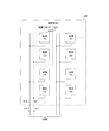
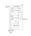
図1は、本技術の第1の実施の形態における電子機器100の一構成例を示すブロック図である。この電子機器100は、画像データを撮像するための機器であり、光学系110、固体撮像素子200、画像処理部120、メモリ130、撮像制御部140およびモニタ150を備える。電子機器100としては、スマートフォン、IoT(Internet of Things)カメラや車載カメラなどが想定される。
<1. First embodiment>
[Configuration Example of Electronic Device]
FIG. 1 is a block diagram showing a configuration example of an
光学系110は、被写体からの入射光を集光して固体撮像素子200に導くものである。光学系110は、1枚以上の光学レンズを含む。
The
固体撮像素子200は、撮像制御部140の制御に従って画像データを撮像するものである。この固体撮像素子200は、撮像した画像データを画像処理部120に信号線209を介して供給する。
The solid-
撮像制御部140は、固体撮像素子200を制御するものである。この撮像制御部140は、撮像タイミングを示す垂直同期信号や、露光時間を制御する信号などを固体撮像素子200に信号線149を介して供給する。また、撮像制御部140は、例えば、撮像を開始させるための操作(シャッターボタンの押下など)が行われたときに、垂直同期信号の供給を開始する。
The
画像処理部120は、画像データに対して、デモザイク処理やホワイトバランス処理などの所定の画像処理を実行するものである。この画像処理部120は、処理後の画像データをメモリ130やモニタ150に信号線128および129を介して供給する。メモリ130は、画像データを記憶するものである。モニタ150は、画像データを表示するものである。
The
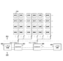
[固体撮像素子の構成例]
図2は、本技術の第1の実施の形態における固体撮像素子200の一構成例を示すブロック図である。この固体撮像素子200は、センサチップ201と、そのセンサチップ201に積層された回路チップ202とを備える。
[Configuration Example of Solid-State Imaging Device]
FIG. 2 is a block diagram showing a configuration example of the solid-
センサチップ201には、複数の画素が二次元格子状に配列された画素領域220が配置される。また、回路チップ202には、垂直駆動回路210、カラム信号処理部240、タイミング制御回路250および出力回路260が配置される。
In the
垂直駆動回路210は、画素を駆動して画素信号をカラム信号処理部240へ出力させるものである。カラム信号処理部240は、列ごとに、画素信号に対してAD(Analog to Digital)変換処理を実行し、出力回路260に供給するものである。出力回路260は、カラム信号処理部240からのデータに対してCDS(Correlated Double Sampling)処理などを実行し、画像処理部120へ出力するものである。また、出力回路260においては、CDS処理の他、画像データのコントラストに基づいて焦点を検出するコントラストAF(Auto Focus)処理が必要に応じて実行される。
The
タイミング制御回路250は、垂直同期信号に同期して、垂直駆動回路210、カラム信号処理部240および出力回路260のそれぞれの動作タイミングを制御するものである。
The
図3は、本技術の第1の実施の形態における画素領域220の平面図の一例である。この画素領域220には、複数の画素230が二次元格子状に、例えば、ベイヤー配列により配列される。ベイヤー配列においては、赤色の画素信号を生成するR(Red)の画素230と、緑色の画素信号を生成するG(Green)の画素230と、青色の画素信号を生成するB(Blue)の画素230とが配列される。なお、画素230は、ベイヤー配列以外の方式により、配列してもよい。
FIG. 3 is an example of a plan view of the
また、画素230の列ごとに、垂直方向に垂直信号線VSL1およびVSL2が配線される。画素領域220内の列の総数をM(Mは、整数)とすると、合計で2×M本の垂直信号線が配線される。垂直方向において隣接する2つの画素230の一方は、垂直信号線VSL1に接続され、他方は垂直信号線VSL2に接続される。例えば、2k(kは、整数)行目の画素230は、垂直信号線VSL1に接続され、2k+1行目の画素230は、垂直信号線VSL2に接続される。これらの2k行目および2k+1行目の2画素からなる集合を、画素ブロック221とする。また、垂直信号線VSL1は、画素信号AINP1を伝送し、垂直信号線VSL2は、画素信号AINP2を伝送する。
Also, for each column of the
垂直駆動回路210は、画素ブロック221の行を順に選択して駆動し、その行において画素ブロック221ごとに画素信号AINP1およびAINP2を同時に出力させる。言い換えれば、垂直駆動回路210は、画素230の2k行目および2k+1行目を同時に駆動する。なお、垂直駆動回路210は、特許請求の範囲に記載の駆動回路の一例である。
The
[画素回路の構成例]
図4は、本技術の第1の実施の形態における画素230の一構成例を示す回路図である。この画素230は、フォトダイオード231、転送トランジスタ232、リセットトランジスタ233、浮遊拡散層234、増幅トランジスタ235および選択トランジスタ236を備える。
[Configuration Example of Pixel Circuit]
FIG. 4 is a circuit diagram showing a configuration example of the
フォトダイオード231は、受光した光を光電変換して電荷を生成するものである。このフォトダイオード231は、半導体基板において回路を配置する面を表面として、表面に対する裏面に配置される。このような固体撮像素子は、裏面照射型の固体撮像素子と呼ばれる。なお、裏面照射型の代わりに、表面にフォトダイオード231を配置する表面照射型の構成を用いることもできる。
The
転送トランジスタ232は、垂直駆動回路210からの転送信号TRGに従ってフォトダイオード231から浮遊拡散層234へ電荷を転送するものである。浮遊拡散層234は、転送された電荷を蓄積して、蓄積した電荷の量に応じた電圧を生成するものである。
The
リセットトランジスタ233は、垂直駆動回路210からのリセット信号RSTpに従って浮遊拡散層234から電荷を引き抜いて、電荷量を初期化するものである。増幅トランジスタ235は、浮遊拡散層234の電圧を増幅するものである。選択トランジスタ236は、垂直駆動回路210からの選択信号SELpに従って、増幅された電圧の信号を画素信号として垂直信号線(例えば、VSL1)を介してカラム信号処理部240へ出力するものである。
The
垂直駆動回路210は、露光が終了する直前の所定のタイミングにおいて、2k行目および2k+1行目に同時にリセット信号RSTpを供給して(言い換えれば、駆動して)画素信号AINP1およびAINP2を同時に出力させる。このリセット時の画素信号のレベルを以下、「リセットレベル」と称する。カラム信号処理部240は、列ごとに2つのリセットレベルを逐次選択してAD変換し、出力回路260へ出力する。
The
また、垂直駆動回路210は、露光終了時のタイミングにおいて、2k行目および2k+1行目に同時に転送信号TRGを供給して(言い換えれば、駆動して)画素信号AINP1およびAINP2を同時に出力させる。この信号転送時の画素信号のレベルを以下、「信号レベル」と称する。カラム信号処理部240は、列ごとに2つの信号レベルを逐次選択してAD変換し、出力回路260へ出力する。
Also, the
そして、出力回路260は、画素230ごとに、リセットレベルと信号レベルとの差分を、kTCノイズ(リセットノイズ)を除去した正味の画素データとして求める。この処理は、CDS処理と呼ばれる。CDS処理により、固体撮像素子200は、ノイズの少ない画像データを撮像することができる。
Then, the
なお、画素230の回路構成は、光電変換により画素信号を生成することができるものであれば、図4に例示した構成に限定されない。
Note that the circuit configuration of the
[カラム信号処理部の構成例]
図5は、本技術の第1の実施の形態におけるカラム信号処理部240の一構成例を示すブロック図である。このカラム信号処理部240は、列ごとに、定電流源241および242とSARADC300とを備える。画素領域220内の画素列の総数をMとすると、合計でM個のSARADC300が配置される。
[Configuration example of column signal processing unit]
FIG. 5 is a block diagram showing a configuration example of the column
定電流源241は、垂直信号線VSL1に一定の電流を供給するものである。定電流源242は、垂直信号線VSL2に一定の電流を供給するものである。
The constant
SARADC300は、対応する列の垂直信号線VSL1およびVSL2に接続される。このSARADC300は、これらの垂直信号線からの画素信号AINP1およびAINP2を逐次選択してAD変換するものである。SARADC300は、AD変換後のデジタル信号DOUTを出力回路260へ出力する。
The
[SARADCの構成例]
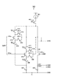
図6は、本技術の第1の実施の形態におけるSARADC300の一構成例を示すブロック図である。このSARADC300は、比較器310、SAR(Successive Approximation Register)ロジック回路350およびDAC(Digital to Analog Converter)360を備える。比較器310の入力端子は、サンプル・ホールド回路を介さずに垂直信号線VSL1およびVSL2と直接接続されている。
[Configuration example of SARADC]
FIG. 6 is a block diagram showing a configuration example of the
ここで、近年、いわゆるスマートフォンやウェアラブルデバイスなどの小型端末で用いられる固体撮像素子は、画素サイズが1マイクロメートル(μm)程度と微細であり、サンプル・ホールド回路を設けるのは困難である。その理由として、サンプル・ホールド回路を設けると、その回路により生じるノイズ(いわゆるkTCノイズ)を抑えるにはサンプル・ホールド回路内の容量を大きくするしかなく、回路面積が増加してしまうためである。また、ADCの入力容量が大きくなってしまう。つまり、垂直信号線の負荷容量が増大することに伴ってセトリング速度が低下してしまい、全体として、処理速度が低下することとなる。また垂直信号線を切り替えた際に、サンプル・ホールド回路の容量を再度充電する必要があり、垂直信号線の切り替えに伴う余分なセトリング時間を必要としてしまう。 Here, in recent years, a solid-state imaging device used in a small terminal such as a so-called smartphone or wearable device has a minute pixel size of about 1 micrometer (μm), and it is difficult to provide a sample and hold circuit. The reason is that if a sample-and-hold circuit is provided, the capacity in the sample-and-hold circuit must be increased to suppress noise (so-called kTC noise) generated by the circuit, and the circuit area increases. In addition, the input capacity of the ADC is increased. That is, as the load capacity of the vertical signal line increases, the settling speed decreases, and as a whole, the processing speed decreases. Further, when switching the vertical signal line, it is necessary to recharge the capacitance of the sample and hold circuit, which requires an extra settling time associated with the switching of the vertical signal line.
これに対し、SARADC300では、サンプルホールド回路を設けずに、垂直信号線を切り替えることが可能であるため、サンプル・ホールド回路を用いる構成によるノイズ発生が生じない。そのため、画質の劣化を抑制することができる。また、サンプル・ホールド回路を設ける場合と比較して、固体撮像素子200の実装面積や消費電力を低減することができる。
On the other hand, in the
比較器310は、タイミング制御回路250の制御に従って画素信号AINP1およびAINP2を逐次選択して、その選択した信号と所定の基準信号AINDACとを比較するものである。この比較器310は、比較結果を示す差動信号をSARロジック回路350に出力する。この差動信号は、正側信号CMPと負側信号xCMPとからなる。
The
ここで、タイミング制御回路250は、信号線選択信号とイネーブル信号ENとを比較器310に供給して、その動作を制御する。信号線選択信号は、垂直信号線VSL1およびVSL2のいずれかを選択させるための信号であり、選択信号SEL1、xSEL1、SEL2、xSEL2からなる。垂直信号線VSL1を選択させる場合には、例えば、選択信号SEL1およびxSEL2がハイレベルに、残りの信号はローレベルに設定される。一方、垂直信号線VSL2を選択させる場合には、例えば、選択信号SEL2およびxSEL1がハイレベルに、残りの信号はローレベルに設定される。
Here, the
また、イネーブル信号ENは、比較器310を有効または無効に制御するための信号である。例えば、比較器310を有効にする場合に、イネーブル信号ENにハイレベルが設定される。一方、比較器310を無効にする場合に、イネーブル信号ENにローレベルが設定される。
The enable signal EN is a signal for controlling the
SARロジック回路350は、比較器310の比較結果に基づいて、画素信号に近似するような基準信号AINDACの値を示すデジタル信号を求めてレジスタに保持し、その値に基準信号AINDACを更新させるための制御信号CTLを生成するものである。DAC360は、制御信号CTLに対するDA(Digital to Analog)変換により、アナログの基準信号AINDACを更新するものである。なお、SARロジック回路350は、特許請求の範囲に記載の制御部の一例である。DAC360は、特許請求の範囲に記載の基準信号更新部の一例である。
The
初期状態において基準信号AINDACのレベルは、所定の参照電圧をVREFとして、例えば、初期値VREF/2に設定される。そして、比較器310は、選択した画素信号と、初期値の基準信号AINDACとを比較する。画素信号が基準信号AINDACより大きい場合、SARロジック回路350は、デジタル信号DOUTのMSB(Most Significant Bit)を「1」にする。そして、SARロジック回路350は、基準信号AINDACをVREF/4の分、上昇させる。
In the initial state, the level of the reference signal AIN DAC is set to, for example, an initial value V REF / 2, with the predetermined reference voltage as V REF . Then, the
一方、画素信号が基準信号AINDAC以下の場合、SARロジック回路350は、デジタル信号DOUTのMSBを「0」にする。そして、SARロジック回路350は、基準信号AINDACをVREF/4の分、降下させる。
On the other hand, if the pixel signal is less than or equal to the reference signal AIN DAC , the
そして、比較器310は、次の比較を行い、画素信号が基準信号AINDACより大きい場合、SARロジック回路350は、MSBの次の桁を「1」にする。そして、SARロジック回路350は、基準信号AINDACをVREF/8の分、上昇させる。
Then, the
一方、画素信号が基準信号AINDAC以下の場合、SARロジック回路350は、MSBの次の桁を「0」にする。そして、SARロジック回路350は、基準信号AINDACをVREF/8の分、降下させる。
On the other hand, if the pixel signal is less than or equal to the reference signal AIN DAC , the
以下、同様の手順が、LSB(Least Significant Bit)まで継続される。これにより、アナログの画素信号が、デジタル信号DOUTにAD変換される。AD変換の終了時にSARロジック回路350は、デジタル信号DOUTを出力回路260に出力する。このデジタル信号DOUTは、画素信号(リセットレベルまたは信号レベル)をAD変換したデータ(すなわち、画素データ)を示す。
Hereinafter, the same procedure is continued until LSB (Least Significant Bit). Thus, the analog pixel signal is AD converted to the digital signal DOUT. At the end of AD conversion, the
なお、タイミング制御回路250は、DAC360の参照電圧VREFを変更することにより、SARADC300のゲインを制御することができる。ゲインは、例えば、「1」乃至「8」倍の範囲で制御される。
Note that the
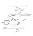
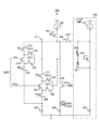
[比較器の構成例]
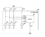
図7は、本技術の第1の実施の形態における比較器310の一構成例を示す回路図である。この比較器310は、カレントミラートランジスタ311および312と、イネーブルスイッチ313と、選択スイッチ314および317と、画素側トランジスタ315および318と、短絡スイッチ316および319とを備える。また、比較器310は、基準側トランジスタ320と、電流源トランジスタ321とを備える。カレントミラートランジスタ311および312として、例えば、pMOS(p-channel Metal Oxide Semiconductor)トランジスタが用いられる。また、画素側トランジスタ315、画素側トランジスタ318、基準側トランジスタ320および電流源トランジスタ321として、例えば、nMOS(n-channel Metal Oxide Semiconductor)トランジスタが用いられる。
[Configuration example of comparator]
FIG. 7 is a circuit diagram showing one configuration example of the
カレントミラートランジスタ311のゲートは、カレントミラートランジスタ312のゲートに接続され、ソースは電源に接続される。また、カレントミラートランジスタ311のドレインは、正側出力ノード322に接続される。カレントミラートランジスタ312のソースは電源に接続され、ドレインは、負側出力ノード323に接続される。
The gate of the
イネーブルスイッチ313は、タイミング制御回路250からのイネーブル信号ENに従って、カレントミラートランジスタ311および312のそれぞれのゲートと負側出力ノード323との間の経路を開閉するものである。例えば、イネーブル信号ENがハイレベル(有効)の場合にイネーブルスイッチ313は閉状態に移行し、イネーブル信号ENがローレベル(無効)の場合にイネーブルスイッチ313は開状態に移行する。カレントミラートランジスタ311および312とイネーブルスイッチ313とからなる回路は、カレントミラー回路として機能する。
The enable
選択スイッチ314は、タイミング制御回路250からの選択信号SEL1に従って画素側トランジスタ315のドレインと正側出力ノード322との間の経路を開閉するものである。例えば、選択信号SEL1がハイレベルである(すなわち、垂直信号線VSL1が選択された)場合に選択スイッチ314は閉状態に移行し、選択信号SEL1がローレベルである場合に選択スイッチ314は開状態に移行する。
The
画素側トランジスタ315のゲートは垂直信号線VSL1に接続され、ソースは電流源トランジスタ321のドレインに接続される。
The gate of the
短絡スイッチ316は、選択信号xSEL1に従って、画素側トランジスタ315のソースおよびドレインを短絡するものである。例えば、選択信号xSEL1がハイレベルである(すなわち、垂直信号線VSL1が選択されていない)場合に短絡スイッチ316は閉状態に移行してソースおよびドレインを短絡する。一方、選択信号xSEL1がローレベルである場合に短絡スイッチ316は、開状態に移行する。
The shorting
選択スイッチ317は、タイミング制御回路250からの選択信号SEL2に従って画素側トランジスタ318のドレインと正側出力ノード322との間の経路を開閉するものである。例えば、選択信号SEL2がハイレベルである(すなわち、垂直信号線VSL2が選択された)場合に選択スイッチ317は閉状態に移行し、選択信号SEL2がローレベルである場合に選択スイッチ317は開状態に移行する。なお、選択スイッチ314および317からなる回路は、特許請求の範囲に記載の比較器内選択部の一例である。
The
画素側トランジスタ318のゲートは垂直信号線VSL2に接続され、ソースは電流源トランジスタ321のドレインに接続される。
The gate of the
短絡スイッチ319は、選択信号xSEL2に従って、画素側トランジスタ318のソースおよびドレインを短絡するものである。例えば、選択信号xSEL2がハイレベルである(すなわち、垂直信号線VSL2が選択されていない)場合に短絡スイッチ319は閉状態に移行してソースおよびドレインを短絡する。一方、選択信号xSEL2がローレベルである場合に短絡スイッチ319は、開状態に移行する。なお、短絡スイッチ316および319からなる回路は、特許請求の範囲に記載の短絡部の一例である。
The shorting
基準側トランジスタ320のゲートには、DAC360からの基準信号AINDACが入力され、ソースは電流源トランジスタ321のドレインに接続され、ドレインは負側出力ノード323に接続される。
The reference signal AIN DAC from the DAC 360 is input to the gate of the
正側出力ノード322および負側出力ノード323からは、正側信号CMPおよび負側信号xCMPがSARロジック回路350へ出力される。これらの正側信号CMPおよび負側信号xCMPからなる差動信号は、選択された垂直信号線からの画素信号と基準信号AINDACとの比較結果を示す。
From positive
電流源トランジスタ321のゲートには一定のバイアス電圧Vbiasが入力され、ソースは、接地端子に接続される。
A constant bias voltage Vbias is input to the gate of the
上述の構成により、垂直信号線VSL1が選択された場合には、選択スイッチ314が閉状態に移行して、画素側トランジスタ315のドレインと正側出力ノード322とを接続する。また、選択スイッチ317は開状態に移行して、選択されない方の画素側トランジスタ318のドレインをハイインピーダンスにする。さらに、短絡スイッチ319は、選択されない方の画素側トランジスタ318のソースおよびドレインを短絡する。
With the configuration described above, when the vertical signal line VSL1 is selected, the
一方、垂直信号線VSL2が選択された場合には、選択スイッチ317が閉状態に移行して、画素側トランジスタ318のドレインと正側出力ノード322とを接続する。また、選択スイッチ314は開状態に移行して、選択されない方の画素側トランジスタ315のドレインをハイインピーダンスにする。さらに、短絡スイッチ316は、選択されない方の画素側トランジスタ315のソースおよびドレインを短絡する。
On the other hand, when the vertical signal line VSL2 is selected, the
このように、選択されない方の画素側トランジスタのドレインをハイインピーダンスにし、そのソースおよびドレインを短絡することにより、選択されない方の垂直信号線からのノイズの影響を抑制することができる。すなわち、ノイズ耐性を向上させることができる。 As described above, by setting the drain of the non-selected pixel transistor to high impedance and shorting the source and the drain, the influence of noise from the non-selected vertical signal line can be suppressed. That is, noise immunity can be improved.
また、イネーブル信号ENをローレベルにすることにより、イネーブルスイッチ313が開状態となるため、比較器310の比較動作を無効にすることができる。タイミング制御回路250は、例えば、AD変換を行わない期間においてイネーブル信号ENにより比較器310を無効にすることによって、消費電力を削減することができる。なお、図8に例示するように、イネーブルスイッチ313を削除し、カレントミラートランジスタ311および312と電流源トランジスタ321とのそれぞれのゲートにイネーブル信号ENを入力してもよい。この場合にタイミング制御回路250は、例えば、比較器310が比較を行うタイミングにおいてイネーブル信号ENをハイレベルにする。また、タイミング制御回路250は、SARロジック回路350がレジスタを更新中の期間や、DAC36の基準信号を更新中の期間においてイネーブル信号ENをローレベルにする。これにより、さらに消費電力を削減することができる。
Further, by setting the enable signal EN to the low level, the enable
図9は、本技術の第1の実施の形態における固体撮像素子200の全体図の一例である。画素ブロック221には、2つの画素230が垂直方向に配列される。垂直駆動回路210は、画素ブロック221を駆動して、2つの画素信号(AINP1およびAINP2)を垂直信号線VSL1およびVSL2を介して同時に出力させる。
FIG. 9 is an example of the entire view of the solid-
そして、SARADC300において、比較器310は、画素信号AINP1およびAINP2を逐次選択して、その信号と基準信号AINDACとを比較する。
Then, in the
SARロジック回路350は、比較器310の比較結果に基づいて、基準信号AINDACを更新させるための制御信号CTLを生成してDAC360に供給する。DAC360は、その制御信号CTLに従って、基準信号AINDACを更新し、比較器310に供給する。
The
[固体撮像素子の動作例]
図10は、本技術の第1の実施の形態における固体撮像素子200の動作の一例を示すタイミングチャートである。垂直駆動回路210は、タイミングT0において、リセット信号RSTpにより画素ブロック221を駆動して、リセットレベルR1およびR2を同時に出力させる。また、タイミング制御回路250は、SARADC300を初期化する。ここで、SARADC300の初期化とは、SARADC300内の基準信号AINDACおよびデジタル信号DOUTを初期値にすることを意味する。
[Operation example of solid-state imaging device]
FIG. 10 is a timing chart showing an example of the operation of the solid-
リセットレベルR1およびR2が静定するまでのセトリングタイムが経過したタイミングT1においてタイミング制御回路250は、選択信号によりSARADC300を制御してリセットレベルR1のAD変換を開始させる。リセットレベルR1のAD変換完了時のタイミングT11においてタイミング制御回路250は、選択信号によりSARADC300を制御してリセットレベルR2のAD変換を開始させる。これらのAD変換が完了するタイミングT2までの間において、アナログのリセットレベルR1およびR2は、保持される。また、AD変換されたリセットレベルは、出力回路260により保持される。
At timing T1 at which the settling time until the reset levels R1 and R2 settle down has elapsed, the
AD変換が完了したタイミングT2において垂直駆動回路210は、転送信号TRGにより画素ブロック221を駆動して、信号レベルS1およびS2を同時に出力させる。また、タイミング制御回路250は、SARADC300を初期化する。
At timing T2 when AD conversion is completed, the
信号レベルS1およびS2が静定するまでのセトリングタイムが経過したタイミングT3においてタイミング制御回路250は、選択信号によりSARADC300を制御して信号レベルS1のAD変換を開始させる。信号レベルS1のAD変換完了時のタイミングT31においてタイミング制御回路250は、選択信号によりSARADC300を制御して信号レベルS2のAD変換を開始させる。これらのAD変換が完了するタイミングT4までの間において、アナログの信号レベルS1およびS2は保持される。そして、出力回路260は、AD変換された信号レベルを取得し、その信号レベルと、保持しておいたリセットレベルとの差分を求める。
At timing T3 at which the settling time for the signal levels S1 and S2 to settle has elapsed, the
上述の画素ブロック221の駆動およびAD変換は、画素ブロック221の行ごとに実行される。画素ブロック221の1行は、画素230の2行に相当するため、タイミングT0やT2において2行を同時に駆動することにより、それらの2行を順に駆動する場合と比較して、画像データの読出し速度を向上させることができる。ここで、読出し速度は、画素230を駆動してからAD変換が完了するまでの時間により、一定値(例えば、画素データのデータサイズ)を除した値を意味する。
The drive and AD conversion of the
また、AD変換をSARADC300により実行するため、シングルスロープ型のADCによりAD変換を実行する場合と比較して、AD変換の速度を速くすることができる。
Further, since the AD conversion is performed by the
図11は、本技術の第1の実施の形態における固体撮像素子200の動作の一例を示すフローチャートである。この動作は、例えば、画像データを撮像するための所定のアプリケーションが実行されたときに開始される。
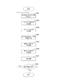
FIG. 11 is a flowchart illustrating an example of the operation of the solid-
固体撮像素子200内の垂直駆動回路210は、まず、2k行目および2k+1行目をリセット信号RSTpにより同時に初期化する(ステップS901)。リセットレベルR1およびR2が静定した後にSARADC300は、リセットレベルR1をAD変換し(ステップS902)、次にリセットレベルR2をAD変換する(ステップS903)。
First, the
そして、垂直駆動回路210は、2k行目および2k+1行目において転送信号TRGにより同時に電荷の転送を行わせる(ステップS904)。信号レベルS1およびS2が静定した後にSARADC300は、信号レベルS1をAD変換し(ステップS905)、次に信号レベルS2をAD変換する(ステップS906)。
Then, the
そして、出力回路260は、CDS処理を実行する(ステップS907)。固体撮像素子200は、全行の読出しが完了したか否かを判断する(ステップS908)。全行の読出しが完了していない場合に(ステップS908:No)、固体撮像素子200は、ステップS901以降を繰り返し実行する。一方、全行の読出しが完了した場合に(ステップS908:Yes)、固体撮像素子200は、画像データを撮像する動作を終了する。複数の画像データを撮像する場合には、例えば、垂直同期信号に同期してステップS901乃至S908が繰り返し実行される。
Then, the
このように、本技術の第1の実施の形態によれば、垂直駆動回路210が2つの画素信号を同時に出力させ、比較器310がそれらを逐次選択して比較することにより、画素信号を1つずつ出力させて比較する場合よりも読出し速度を向上させることができる。
As described above, according to the first embodiment of the present technology, the
[第1の変形例]
上述の第1の実施の形態では、固体撮像素子200は、コントラストAF方式を用いて焦点を検出していたが、コントラストAFは、位相差AF方式と比較して、AF速度が遅くなってしまう。この第1の実施の形態の変形例の固体撮像素子200は、位相差AF方式を用いて焦点を検出する点において第1の実施の形態と異なる。
[First Modification]
In the first embodiment described above, the solid-
図12は、本技術の第1の実施の形態の変形例における画素領域220の平面図の一例である。この第1の実施の形態の変形例の画素領域220には、長方形の画素が配列される。
FIG. 12 is an example of a plan view of a
また、画素領域220においては、同色の一対の画素が、水平方向に隣接して配列される。例えば、Gの画素291の右側にGの画素292が配置される。その画素292の右側に一対のB画素が配列される。画素291および292の下方には一対のR画素が配置され、それらの右側には2つのG画素が配置される。
Further, in the
そして、隣接する同色の一対の画素には、同一のマイクロレンズが設けられる。図11における一点鎖線は、マイクロレンズの位置を表す。これらの一対の画素の一方には、瞳分割された2つの像の一方の入射光が入力され、一対の画素の他方には、瞳分割された2つの像の他方の入射光が入力される。出力回路260は、画素データから2つの像の位相差を求め、その位相差から焦点を検出する位相差AF処理を実行する。
The same microlens is provided in a pair of adjacent pixels of the same color. The dashed-dotted line in FIG. 11 represents the position of the microlens. The incident light of one of the two pupil-divided images is input to one of the pair of pixels, and the other incident light of the two pupil-divided images is input to the other of the pair of pixels . The
このように、本技術の第1の実施の形態の変形例によれば、位相差AF方式を用いることにより、コントラストAF方式を用いる場合と比較して、高速に焦点を検出することができる。 As described above, according to the modification of the first embodiment of the present technology, the use of the phase difference AF method makes it possible to detect the focus at high speed as compared with the case of using the contrast AF method.
<2.第2の実施の形態>
上述の第1の実施の形態では、画素230ごとに、浮遊拡散層234や選択トランジスタ236を配置していたが、画素数が多くなるほど回路規模が増大するおそれがある。この第2の実施の形態の固体撮像素子200は、複数の画素が浮遊拡散層等を共有する点において第1の実施の形態と異なる。
<2. Second embodiment>
In the first embodiment described above, the floating
図13は、本技術の第2の実施の形態における画素領域220の平面図の一例である。第2の実施の形態の画素領域220において、画素ブロック221には、2つの共有ブロック270が垂直方向に配列される。それぞれの共有ブロック270には、浮遊拡散層を共有する複数の画素が配列される。例えば、4行×2列の8画素が共有ブロック270に配列される。これらの画素は、第1の実施の形態と同様にベイヤー配列により配列される。なお、共有ブロック270内の画素数は、8個に限定されない。
FIG. 13 is an example of a plan view of the
また、SARADC300は、画素ブロック221の列ごとに配列される。言い換えれば、SARADC300は、画素の2列ごとに配列される。また、垂直信号線は、画素ブロック221の列ごとに2本配線される。例えば、画素領域220内の画素列の総数をMとすると、SARADC300は、合計でM/2個配列され、垂直信号線は、合計でM本配線される。また、画素ブロック221内の2つの共有ブロック270は、互いに異なる垂直信号線に接続される。
In addition, the
図14は、本技術の第1の実施の形態における共有ブロック270の一構成例を示す回路図である。この共有ブロック270は、転送トランジスタ271、272、275、276、279、280、283および284と、フォトダイオード273、274、277、278、281、282、285および286とを備える。また、共有ブロック270は、リセットトランジスタ287、浮遊拡散層288、増幅トランジスタ289および選択トランジスタ290を備える。転送トランジスタ271等のトランジスタとして、例えば、nMOSトランジスタが用いられる。
FIG. 14 is a circuit diagram showing one configuration example of the shared
フォトダイオード273、274、277、278、281、282、285および286のそれぞれは、受光した光を光電変換して電荷を生成するものである。
Each of the
転送トランジスタ271は、垂直駆動回路210からの転送信号TRG0に従ってフォトダイオード273から浮遊拡散層288へ電荷を転送するものである。転送トランジスタ272は、垂直駆動回路210からの転送信号TRG1に従ってフォトダイオード274から浮遊拡散層288へ電荷を転送するものである。
The
転送トランジスタ275は、垂直駆動回路210からの転送信号TRG2に従ってフォトダイオード277から浮遊拡散層288へ電荷を転送するものである。転送トランジスタ276は、垂直駆動回路210からの転送信号TRG3に従ってフォトダイオード278から浮遊拡散層288へ電荷を転送するものである。
The
また、転送トランジスタ279は、垂直駆動回路210からの転送信号TRG4に従ってフォトダイオード281から浮遊拡散層288へ電荷を転送するものである。転送トランジスタ280は、垂直駆動回路210からの転送信号TRG5に従ってフォトダイオード282から浮遊拡散層288へ電荷を転送するものである。
Further, the
転送トランジスタ283は、垂直駆動回路210からの転送信号TRG6に従ってフォトダイオード285から浮遊拡散層288へ電荷を転送するものである。転送トランジスタ284は、垂直駆動回路210からの転送信号TRG7に従ってフォトダイオード286から浮遊拡散層288へ電荷を転送するものである。
The
浮遊拡散層288は、転送された電荷を蓄積して、蓄積した電荷の量に応じた電圧を生成するものである。リセットトランジスタ287は、垂直駆動回路210からのリセット信号RSTpに従って浮遊拡散層288から電荷を引き抜いて、電荷量を初期化するものである。増幅トランジスタ289は、浮遊拡散層288の電圧を増幅するものである。選択トランジスタ290は、垂直駆動回路210からの選択信号SELpに従って、増幅された電圧の信号を画素信号として垂直信号線VSL1等を介してカラム信号処理部240へ出力するものである。
The floating
垂直駆動回路210は、画素ブロック221を駆動して、上側の共有ブロック270内のいずれかの画素の画素信号と下側の共有ブロック270内のいずれかの画素の画素信号とを同時に出力させる。
The
このように、本技術の第2の実施の形態によれば、複数の画素が浮遊拡散層288や選択トランジスタ290を共有するため、浮遊拡散層288等を共有しない構成と比較して、画素当たりの回路規模を削減することができる。
As described above, according to the second embodiment of the present technology, the plurality of pixels share the floating
[変形例]
上述の第2の実施の形態では、ベイヤー配列により画素を画素領域220に配列していたが、ベイヤー配列では同色の画素が隣り合っていないため、同色の複数の画素データを画素加算する際に画質が低下するおそれがある。この第2の実施の形態の変形例の固体撮像素子200は、同色の複数の画素を隣接して配置した点において第2の実施の形態と異なる。
[Modification]
In the second embodiment described above, the pixels are arranged in the
図15は、本技術の第2の実施の形態の変形例における画素領域220の平面図の一例である。同図に例示するように、第2の実施の形態の変形例では、同色の4個の画素が隣接して配置される。例えば、Gの画素293が共有ブロック270の左上に配置され、その右側にGの画素294が配置される。また、画素293の下方にGの画素295が配置され、その右側にGの画素296が配置される。共有ブロック270において残りには、R画素が4つ配置される。その右側の共有ブロック270には、4個のB画素と4個のG画素とが配置される。
FIG. 15 is an example of a plan view of a
出力回路260は、画素加算モードなどにおいて、隣接する同色の4個の画素データを画素加算する。
The
また、垂直駆動回路210は、ダイナミックレンジを拡大するモードにおいて、隣接する同色の4個の画素のうち半分の露光時間を、残りの露光時間と異なる値に設定する。例えば、垂直駆動回路210は、画素293と、その右下の画素296とを露光時間TSに亘って露光させる。次に、垂直駆動回路210は、画素294と、その左下の画素295とを、露光時間TSより長い露光時間TLに亘って露光させる。そして、出力回路260は、露光時間TSで露光した画素データと、露光時間TLで露光した画素データとをアルファ合成などにより合成する。これにより、ダイナミックレンジを拡大することができる。
Also, in the mode for expanding the dynamic range, the
このように、本技術の第2の実施の形態の変形例によれば、同色の複数の画素を隣接して配置したため、隣接する画素の色が異なるベイヤー配列の場合と比較して、画素加算した画像データの画質を向上させることができる。 As described above, according to the modification of the second embodiment of the present technology, since the plurality of pixels of the same color are arranged adjacent to each other, pixel addition is performed as compared to the Bayer arrangement in which adjacent pixels have different colors. It is possible to improve the image quality of the processed image data.
<3.第3の実施の形態>
上述の第1の実施の形態では、SARADC300内にサンプル・ホールドを行うためのキャパシタを配置していなかった。しかし、この構成では、AD変換に要する時間が長くなると、画素230が保持した画素信号のレベルが変動して、AD変換の誤差が大きくなるおそれがある。この第3の実施の形態のSARADC300は、キャパシタを備える点において第1の実施の形態と異なる。
<3. Third embodiment>
In the first embodiment described above, no capacitor for sample and hold is arranged in the
図16は、本技術の第3の実施の形態におけるSARADC300の一構成例を示すブロック図である。この第3の実施の形態のSARADC300は、キャパシタ381および382と、リセットスイッチ371および372とをさらに備える点において第1の実施の形態と異なる。
FIG. 16 is a block diagram showing a configuration example of the
キャパシタ381の一端は垂直信号線VSL1に接続され、他端は比較器310の入力端子に接続される。キャパシタ382の一端は垂直信号線VSL2に接続され、他端は比較器310の入力端子に接続される。
One end of the
リセットスイッチ371は、タイミング制御回路250からのリセット信号RSTaに従って、キャパシタ381の比較器310側の端子と、低インピーダンスの固定電位との間の経路を開閉するものである。リセットスイッチ372は、リセット信号RSTaに従って、キャパシタ382の比較器310側の端子と固定電位との間の経路を開閉するものである。例えば、リセット信号RSTaがハイレベルの場合にリセットスイッチ371および372は閉状態に移行する。これにより、キャパシタ381および382のそれぞれの電荷量が初期化される。一方、リセット信号RSTaがローレベルの場合にリセットスイッチ371および372は開状態に移行し、ハイインピーダンスとなる。なお、リセットスイッチ371および372からなる回路は、特許請求の範囲に記載のリセット部の一例である。
The
図17は、本技術の第3の実施の形態における固体撮像素子200の動作の一例を示すタイミングチャートである。画素ブロック221が初期化されるタイミングT0から、セトリングタイムが経過するタイミングT1までの間において、タイミング制御回路250は、リセット信号RSTaによりリセットスイッチ371および372を閉状態にする。これにより、キャパシタ381および382の電荷量が初期化される。
FIG. 17 is a timing chart showing an example of the operation of the solid-
そして、タイミングT1において、タイミング制御回路250は、リセット信号RSTaによりリセットスイッチ371および372を開状態にする。これにより、リセットスイッチ371および372はハイインピーダンスとなる。このときに、リセットノイズがキャパシタ381および382に保持される。一方、画素230もリセットレベルを保持し続ける。そして、リセットレベルのAD変換が完了するタイミングT3まで、タイミング制御回路250は、リセットスイッチ371および372を開状態に維持する。
Then, at timing T1, the
また、タイミングT2から信号レベルが静定するタイミングT3までの間においても、タイミング制御回路250は、リセットスイッチ371および372を開状態のままにする。これにより、キャパシタ381および382の片側が解放端のままの状態であり続けるため、容量電荷が移動せず、新たにkTCノイズが印加されることを回避することができる。タイミングT3から、次に画素230をリセットするタイミングまで、タイミング制御回路250は、リセットスイッチ371および372を開状態に維持する。
Further, the
なお、第3の実施の形態では、画素230ごとに、浮遊拡散層234等を配置しているが、第2の実施の形態のように、複数の画素が浮遊拡散層等を共有する構成としてもよい。
In the third embodiment, the floating
このように、本技術の第3の実施の形態によれば、SARADC300内に画素信号を保持するキャパシタ381および382を設けることにより、AD変換中の画素信号の変動を抑制することができる。
As described above, according to the third embodiment of the present technology, by providing the
<4.第4の実施の形態>
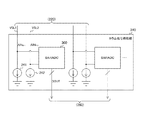
上述の第1の実施の形態では、1つのカラム信号処理部240が2k行目と2k+1行目の画素信号を逐次選択してAD変換していたが、行数が増大するほど、AD変換の回数が増加し、読出し速度が低下してしまう。この第4の実施の形態の固体撮像素子200は、2つのカラム信号処理部を配置した点において第1の実施の形態と異なる。
<4. Fourth embodiment>
In the above-described first embodiment, one column
図18は、本技術の第4の実施の形態における固体撮像素子200の一構成例を示すブロック図である。この固体撮像素子200は、カラム信号処理部240の代わりに、上側カラム信号処理部245と下側カラム信号処理部246とを備える点において第1の実施の形態と異なる。
FIG. 18 is a block diagram showing a configuration example of a solid-
画素ブロック221には、4つの画素230が垂直方向に配列される。また、垂直駆動回路210は、それらの画素230を駆動して4k行目と4k+1行目の画素信号を上側カラム信号処理部245に出力させ、4k+2行目と4k+3行目の画素信号とを下側カラム信号処理部246に出力させる。
In the
上側カラム信号処理部245は、4k行目と4k+1行目の画素信号をAD変換し、下側カラム信号処理部246は、4k+2行目と4k+3行目の画素信号をAD変換する。
The upper column
なお、第4の実施の形態では、画素230ごとに、浮遊拡散層234等を配置しているが、第2の実施の形態のように、複数の画素が浮遊拡散層等を共有する構成としてもよい。
In the fourth embodiment, the floating
このように、本技術の第4の実施の形態によれば、上側カラム信号処理部245と下側カラム信号処理部246とが並列にAD変換を行うことにより、それらの一方のみを設ける場合と比較して読出し速度を2倍にすることができる。
As described above, according to the fourth embodiment of the present technology, the upper column
<5.第5の実施の形態>
上述の第1の実施の形態では、列ごとにSARADC300を配置していたが、列数が増大するほど、SARADC300の個数が多くなり、カラム信号処理部240の回路規模が大きくなるおそれがある。この第5の実施の形態の固体撮像素子200は、2列ごとにSARADC300を配置した点において第1の実施の形態と異なる。
<5. Fifth embodiment>
In the first embodiment described above, the
図19は、本技術の第5の実施の形態の変形例における画素領域220の平面図の一例である。第5の実施の形態の画素領域220においては、画素ブロック221ごとに、2行×2列に4つの画素230が配列される。また、2列ごとに、垂直信号線VSL1乃至VSL4の4本が配線される。画素領域220内の画素列の総数をMとすると、合計で2×M本の垂直信号線が配線される。画素ブロック221内の4画素は、互いに異なる垂直信号線に接続される。
FIG. 19 is an example of a plan view of a
なお、画素ブロック221内に4画素を配列して、画素ブロック221の列ごとに4本の垂直信号線を配線しているが、垂直信号線の本数は2本以上であれば、4本に限定されない。すなわち、画素ブロック221内にN(Nは2以上の整数)画素を配列して、N本の垂直信号線を配線することができる。ただし、Nは、2乃至16が妥当な値である。
Although four pixels are arranged in the
また、第5の実施の形態では、画素230ごとに、浮遊拡散層234等を配置しているが、第2の実施の形態のように、複数の画素が浮遊拡散層等を共有する構成としてもよい。
In the fifth embodiment, the floating
図20は、本技術の第5の実施の形態におけるカラム信号処理部240の一構成例を示すブロック図である。この第5の実施の形態のカラム信号処理部240は、2列ごとに、定電流源241、242、243および244とSARADC300とを備える。画素領域220内の画素列の総数をMとすると、合計でM/2個のSARADC300が配置される。SARADC300ごとの垂直信号線をN本とする場合には、図21に例示するように、N本の垂直信号線がSARADC300に入力される。
FIG. 20 is a block diagram showing a configuration example of a column
図22は、本技術の第5の実施の形態におけるSARADC300の一構成例を示すブロック図である。この第5の実施の形態のSARADC300は、キャパシタ381、382、383および384と、リセットスイッチ371、372、373および274とをさらに備える点において第1の実施の形態と異なる。
FIG. 22 is a block diagram illustrating a configuration example of the
リセットスイッチ371および372と、キャパシタ381および382との接続構成は、第3の実施の形態と同様である。
The connection configuration between the reset switches 371 and 372 and the
キャパシタ383の一端は垂直信号線VSL3に接続され、他端は比較器310の入力端子に接続される。キャパシタ384の一端は垂直信号線VSL4に接続され、他端は比較器310の入力端子に接続される。
One end of the
リセットスイッチ373は、タイミング制御回路250からのリセット信号RSTaに従って、キャパシタ383の比較器310側の端子と、固定電位との間の経路を開閉するものである。リセットスイッチ374は、リセット信号RSTaに従って、キャパシタ384の比較器310側の端子と固定電位との間の経路を開閉するものである。
The
また、比較器310には、選択スイッチ314、画素側トランジスタ315および短絡スイッチ316からなる回路と同様の回路が、垂直信号線VSL3およびVSL4のそれぞれについて、さらに追加される。
In addition, in the
図23は、本技術の第5の実施の形態における固体撮像素子200の動作の一例を示すタイミングチャートである。タイミング制御回路250は、タイミングT0において、リセット信号RSTpにより画素ブロック221を駆動して、リセットレベルR1乃至R4を同時に出力させる。また、タイミング制御回路250は、SARADC300を初期化する。
FIG. 23 is a timing chart showing an example of the operation of the solid-
セトリングタイムが経過したタイミングT1においてタイミング制御回路250は、選択信号によりSARADC300を制御してリセットレベルR1のAD変換を開始させる。リセットレベルR1のAD変換完了時のタイミングT11においてタイミング制御回路250は、リセットレベルR2のAD変換を開始させる。そしてタイミング制御回路250は、リセットレベルR2のAD変換完了時のタイミングT12においてリセットレベルR3のAD変換を開始させ、リセットレベルR3のAD変換完了時のタイミングT13においてリセットレベルR4のAD変換を開始させる。
At timing T1 when the settling time has elapsed, the
AD変換が完了したタイミングT2において垂直駆動回路210は、転送信号TRGにより画素ブロック221を駆動して、信号レベルS1乃至S4を同時に出力させる。また、タイミング制御回路250は、SARADC300を初期化する。
At timing T2 when AD conversion is completed, the
セトリングタイムが経過したタイミングT3においてタイミング制御回路250は、選択信号によりSARADC300を制御して信号レベルS1のAD変換を開始させる。信号レベルS1のAD変換完了時のタイミングT31においてタイミング制御回路250は、信号レベルS2のAD変換を開始させる。そしてタイミング制御回路250は、信号レベルS2のAD変換完了時のタイミングT32において信号レベルS3のAD変換を開始させ、信号レベルS3のAD変換完了時のタイミングT33において信号レベルS4のAD変換を開始させる。なお、リセットスイッチ371乃至374の制御タイミングは、第3の実施の形態と同様である。
At timing T3 when the settling time has elapsed, the
ここで、固体撮像素子が、2k行目のリセット(または電荷転送)と並列に、2k+1行目の画素信号のAD変換を実行するパイプライン処理を実行する方法も考えられる。しかし、このパイプライン処理では、パイプライン処理を実行しない場合と比較して読出し速度を2倍までしか高速化することができない。これは、垂直信号線の駆動速度は、AD変換速度と比較して遅く、セトリングタイムにより律速されてしまい、パイプライン処理そのものを高速化することができないためである。 Here, a method is also conceivable in which the solid-state imaging device executes pipeline processing in which AD conversion of pixel signals on the 2k + 1st row is performed in parallel with resetting (or charge transfer) on the 2kth row. However, in this pipeline processing, the read speed can be speeded up by only twice as compared with the case where pipeline processing is not performed. This is because the driving speed of the vertical signal line is slower than the AD conversion speed, and is limited by the settling time, and the pipeline processing itself can not be speeded up.
これに対して、固体撮像素子200では、パイプライン処理を行っておらず、複数の画素を同時にリセットし、セトリング後のタイミングT1以降に逐次選択してAD変換している。このため、読出し速度がセトリングタイムにより律速されることがなく、読出し速度を2倍よりも速くすることができる。
On the other hand, in the solid-
このように、本技術の第5の実施の形態によれば、2列ごとにSARADC300を配置することにより、列ごとにSARADC300を配置する場合と比較して、SARADC300の個数を削減することができる。これにより、カラム信号処理部240の回路規模、実装面積や消費電力を低減することができる。
As described above, according to the fifth embodiment of the present technology, arranging the
<6.第6の実施の形態>
上述の第1の実施の形態では、列ごとにSARADC300を配置していたが、列数が増大するほど、SARADC300の個数が多くなり、カラム信号処理部240の回路規模が大きくなるおそれがある。この第6の実施の形態の固体撮像素子200は、SARADC300の前段にマルチプレクサを配置した点において第1の実施の形態と異なる。
<6. Sixth embodiment>
In the first embodiment described above, the
図24は、本技術の第6の実施の形態における画素領域220の平面図の一例である。この第6の実施の形態の画素領域220において、画素ブロック221のそれぞれには、4行×2列の8個の共有ブロック270が配列される。それぞれの共有ブロック270の構成は、第2の実施の形態と同様である。また、共有ブロック270の2列(言い換えれば、画素の4列)ごとに、垂直信号線VSL1乃至VSL8の8本が配線される。画素領域220内の画素列の総数をMとすると、垂直信号線は、合計で2×M本配線される。画素ブロック221内の共有ブロック270は、互いに異なる垂直信号線に接続される。
FIG. 24 is an example of a plan view of the
また、固体撮像素子200には、第4の実施の形態と同様に上側カラム信号処理部245と下側カラム信号処理部246とが配置される。
Further, in the solid-
垂直駆動回路210は、画素ブロック221を駆動して、それぞれの共有ブロック270に1個の画素信号を出力させる。共有ブロック270は、8個であるため、8個の画素信号が同時に出力される。これらの8個の画素信号のうち4個は、上側カラム信号処理部245によりAD変換され、残りの4個は、下側カラム信号処理部246によりAD変換される。例えば、2個のR画素の画素信号と2個のB画素の画素信号とを上側カラム信号処理部245がAD変換し、4個のG画素の画素信号を下側カラム信号処理部246がAD変換する。
The
なお、画素ブロック221内の共有ブロック270の個数は8個に限定されず、共有ブロック270内の画素数も8個に限定されない。
The number of shared
図25は、本技術の第6の実施の形態における下側カラム信号処理部246の一構成例を示すブロック図である。この下側カラム信号処理部246は、画素ブロック221の列(言い換えれば、画素の4列)ごとに、マルチプレクサ247、SARADC300、定電流源241および定電流源242を2個ずつ備える。画素領域220内の画素列の総数をM列とすると、マルチプレクサ247やSARADC300は、合計でM/2個ずつ配置される。上側カラム信号処理部245の構成は、下側カラム信号処理部246と同様である。
FIG. 25 is a block diagram showing a configuration example of the lower column
マルチプレクサ247は、タイミング制御回路250からの選択信号に従って、垂直信号線VSL1乃至VSL8のうち2本を選択するものである。このマルチプレクサ247は、選択した2本からの画素信号をSARADC300へ出力する。
The
タイミング制御回路250は、下側カラム信号処理部246が処理する4個の画素信号のうち、2個を伝送する垂直信号線を1個目のマルチプレクサ247に選択させ、残りを2個目のマルチプレクサ247に選択させる。なお、マルチプレクサ247は、特許請求の範囲に記載の比較器外選択部の一例である。
The
また、垂直信号線VSL1乃至VSL8は、回路チップ202内で分岐して2個のマルチプレクサ247に入力される。図23における四角のマークは、チップの境界の端子を示す。なお、チップの境界は、この構成に限定されない。例えば、マルチプレクサ247の入力端子をチップの境界としてもよいし、マルチプレクサ247の出力端子をチップの境界としてもよい。
Also, the vertical signal lines VSL1 to VSL8 branch in the
このように、本技術の第6の実施の形態によれば、マルチプレクサ247が8個の画素信号のうち2個を選択し、それらをSARADC300が逐次比較することにより、2列ごとにSARADC300を配置することができる。これにより、カラム信号処理部240の回路規模、実装面積や消費電力を低減することができる。
Thus, according to the sixth embodiment of the present technology, the
<7.第7の実施の形態>
上述の第1の実施の形態では、垂直方向に並んだ画素を同じSARADC300でAD変換するために、そのリニアリティのばらつきに起因して画像データにおいて縦筋が生じるおそれがある。この第7の実施の形態のSARADC300は、DAC360内の容量の組合せをランダムに変更して、制御を行うことで縦筋を抑制する点において第1の実施の形態と異なる。
<7. Seventh embodiment>
In the first embodiment described above, since the pixels arranged in the vertical direction are subjected to AD conversion by the
図26は、本技術の第7の実施の形態におけるDAC360の一構成例を示すブロック図である。このDAC360は、容量361−1乃至361−7と、容量362−1乃至362−13と、電位制御スイッチ363−1乃至363−20とを備える。これらの容量361−1乃至361−7と、容量362−1乃至362−13とのそれぞれの一端は、共通に比較器310の入力端子に接続され、その電位の信号が基準信号AINDACとして供給される。
FIG. 26 is a block diagram showing a configuration example of a
容量361−1乃至361−7は、デジタル信号DOUTの上位の所定ビット(例えば、上位3ビット)を生成するために用いられる容量であり、画素ブロック221の行が選択されるたびに、組合せがランダムに変更される。例えば、これらの容量の値は全て同一であり、所定の単位容量値をCとして、16Cに設定される。
The capacitors 361-1 to 361-7 are capacitors used to generate upper predetermined bits (for example, upper 3 bits) of the digital signal DOUT, and the combination is selected each time the row of the
容量362−1乃至362−13は、デジタル信号DOUTの下位の所定ビット(例えば、5ビット目からLSBまで)を生成するために用いられる容量である。例えば、8C、4C、2C、1Cおよび0.5Cなどの各種の容量値が設定される。 The capacitors 362-1 to 362-13 are capacitors used to generate lower predetermined bits (for example, the fifth bit to the LSB) of the digital signal DOUT. For example, various capacitance values such as 8C, 4C, 2C, 1C and 0.5C are set.
電位制御スイッチ363−1乃至363−20は、容量361−1乃至361−7と容量362−1乃至362−13とのそれぞれの両端のうち比較器310に接続されていない方の一端の電位を変更するものである。電位制御スイッチ363−1乃至363−20のそれぞれには互いに異なる容量が対応付けられ、それらのスイッチは、対応する容量の一端を互いに異なる電位VRC、VRTおよびVRBのいずれかに接続する。例えば、電位VRCは、初期値の電位であり、初期状態において全ての容量は電位VRCに接続される。電位VRTは、電位VRCより高い電位(VRCの2倍など)であり、電位VRBは、電位VRCより低い電位(接地電位など)である。
The potential control switches 363-1 to 363-20 have a potential at one end of each of the capacitors 361-1 to 361-7 and the capacitors 362-1 to 362-13 which are not connected to the
また、電位制御スイッチ363−1乃至363−20には、SARロジック回路350からの制御信号CTLenおよびCTLudが入力され、それぞれのスイッチは、それらの制御信号に従って接続先を切り替える。
Further, control signals CTLen and CTLud from the
制御信号CTLenは、容量ごとに、その容量の一端の電位をVRCに接続するか否かを示す信号である。例えば、容量が20個である場合、制御信号CTLenのデータサイズは、20ビットである。 The control signal CTLen is a signal indicating, for each capacitor, whether or not to connect the potential at one end of the capacitor to the VRC. For example, when the capacity is 20, the data size of control signal CTLen is 20 bits.
制御信号CTLudは、容量ごとに、その容量の一端の電位を電位VRT、VRBの接続するか否かを示す信号である。例えば、容量が20個である場合、制御信号CTLudのデータサイズは、20ビットである。 The control signal CTLud is a signal indicating whether or not the potential of one end of the capacitor is connected to the potential VRT or VRB for each capacitor. For example, when the capacity is 20, the data size of the control signal CTLud is 20 bits.
図27は、本技術の第7の実施の形態におけるSARロジック回路350の一構成例を示すブロック図である。このSARロジック回路350は、下位ビット生成部351、上位ビット生成部352および疑似乱数生成部353を備える。
FIG. 27 is a block diagram showing a configuration example of the
下位ビット生成部351は、逐次比較制御により、容量362−1乃至362−13に対応する下位ビットを生成するものである。ここで、下位ビットの生成において、制御信号CTLen、制御信号CTLudにより指定される容量の順序は固定である。例えば、逐次比較5ビット目を生成する際は、容量362−1が指定され、次の6ビット目を生成する際は、容量362−2が指定される。
The lower
上位ビット生成部352は、逐次比較制御により、容量361−1乃至361−7に対応する上位ビットを生成するものである。この上位ビットの生成において、制御信号CTLen、制御信号CTLudにより指定される容量の組合せは、画素の行が選択されるたびに変更される。
The
疑似乱数生成部353は、上位ビット生成部352の制御に従って疑似乱数を生成するものである。
The pseudo random
下位ビット生成部351および上位ビット生成部352は、比較器310の比較結果に基づいて制御信号CTLenおよびCTLudを生成してDAC360に供給し、デジタル信号DOUTを生成して出力する。
The
この逐次比較制御において、上位ビット生成部352は、例えば、逐次比較2ビット目の基準信号AINDACを生成する際に、4ビットを論理値「1」にし、残りを論理値「0」にした7ビットの疑似乱数を疑似乱数生成部353に生成させる。そして、上位ビット生成部352は、その4ビットに対応した制御信号CTLen、制御信号CTLudをDAC360に供給する。
In this successive approximation control, for example, when generating the reference signal AIN DAC of the second bit of the successive approximation, the upper
そして、逐次比較3ビット目の基準信号AINDACを生成する際に、上位ビット生成部352は、2ビット目の生成時に論理値「1」にしたビットを除く3ビットのうち2ビットを論理値「1」にした7ビットの疑似乱数を疑似乱数生成部353に生成させる。上位ビット生成部352は、その2ビットに対応した制御信号CTLen、制御信号CTLudをDAC360に供給する。
Then, when generating the reference signal AIN DAC of the 3rd bit of successive approximation, the upper
続いて、逐次比較4ビット目の基準信号AINDACを生成する際に、上位ビット生成部352は、逐次比較2ビット目生成時と逐次比較3ビット目生成時とに論理値「1」にしたビットを除く残りの1ビットに対応した制御信号CTLen、制御信号CTLudをDAC360に供給する。
Subsequently, when generating the reference signal AIN DAC of the fourth bit of successive approximation, the upper
図28は、本技術の第7の実施の形態における画素信号の1行目の逐次比較4ビット目までのDAC360の制御例を説明するための図である。同図におけるaは、2ビット目を生成する際のDAC360の状態の一例を示す図である。同図におけるbは、3ビット目を生成する際のDAC360の状態の一例を示す図であり、同図におけるcは、4ビット目を生成する際のDAC360の状態の一例を示す図である。
FIG. 28 is a diagram for describing an example of control of the
まず、上位ビット生成部352は、比較器310の比較結果に基づいて基準信号AINDACを生成する。そして、逐次比較2ビット目の基準信号AINDACを生成する際に、上位ビット生成部352は、7ビットの疑似乱数により、容量361−1乃至361−7のうちランダムに4つを選択する。例えば、2進数で「1111000」の疑似乱数が生成された場合、容量361−1乃至361−4が選択される。これらの容量値が16Cである場合、64Cの合成容量が得られる。また、上位ビット生成部352は、前回の比較器310の比較結果に基づいて電位VRTおよびVRBのいずれに接続するかを指定する。例えば、比較結果CMPが論理値「1」であった場合には、基準信号AINDACを上昇させるため、同図におけるaに例示するように容量361−1乃至361−4を電位VRTに接続させる。
First, the
そして、逐次比較3ビット目の基準信号AINDACを生成する際に、上位ビット生成部352は、7ビットの疑似乱数により、既に選択済みの4つを除いた残り3つの容量のうちからランダムに2つを選択する。例えば、2進数で「0000110」の疑似乱数が生成された場合、容量361−5および361−6が選択される。これらの容量値が16Cである場合、32Cの合成容量が得られる。また、上位ビット生成部352は、前回の比較器310の比較結果に基づいて電位VRTおよびVRBのいずれに接続するかを指定する。例えば、比較結果CMPが論理値「0」であった場合には、基準信号AINDACを降下させるため、同図におけるaに例示するように容量361−5および361−6を、電位VRBに接続させる。
Then, when generating the reference signal AIN DAC of the third bit of successive approximation, the upper
そして、逐次比較4ビット目の基準信号AINDACを生成する際に、上位ビット生成部352は、既に選択済みの6つを除いた残り1つの容量を選択する。例えば、容量361−7が選択され、この容量値は16Cである。また、上位ビット生成部352は、前回の比較器310の比較結果に基づいて電位VRTおよびVRBのいずれに接続するかを指定する。例えば、比較結果CMPが論理値「1」であった場合には、基準信号AINDACを上昇させるため、同図におけるaに例示するように容量361−7を、電位VRTに接続させる。
Then, when generating the reference signal AIN DAC of the fourth bit of the successive approximation, the upper
なお、上記の例ではビット生成毎に疑似乱数の生成を実施したが、逐次比較2ビット目を生成する際に逐次比較4ビット目までの疑似乱数を一度に生成してもよい。この場合には、疑似乱数生成部353内などに、疑似乱数を保持するためのメモリが追加され、SARロジック回路350は、そのメモリから疑似乱数を読み出して容量の組合せを変更する。
In the above example, pseudo random numbers are generated for each bit generation, but when generating the second bit of sequential comparison, pseudo random numbers of up to the fourth bit of sequential comparison may be generated at one time. In this case, a memory for holding the pseudo random number is added in the pseudo random
5ビット目以降は、下位ビット生成部351により固定の順序で容量が選択される。
For the fifth and subsequent bits, the lower
図29は、本技術の第7の実施の形態における画素信号2行目の逐次比較4ビット目までのDAC360の制御例を説明するための図である。同図におけるaは、2ビット目を生成する際のDAC360の状態の一例を示す図である。同図におけるbは、3ビット目を生成する際のDAC360の状態の一例を示す図であり、同図におけるcは、4ビット目を生成する際のDAC360の状態の一例を示す図である。
FIG. 29 is a diagram for describing a control example of the
逐次比較2ビット目生成時に2進数で「0011110」の疑似乱数が生成された場合、同図におけるaに例示するように、容量361−3乃至361−6が選択される。3ビット目生成時に2進数で「1100000」の疑似乱数が生成された場合、同図におけるbに例示するように、容量361−1および361−2が選択される。4ビット目生成時には、同図におけるcに例示するように、残りの容量361−7が選択される。 When a pseudo-random number "0011110" in binary is generated at the time of generation of the successive approximation second bit, the capacities 361-3 to 361-6 are selected as exemplified in a in the figure. When a pseudo-random number of “1100000” is generated in binary at the time of generation of the third bit, the capacities 361-1 and 361-2 are selected as exemplified in b in FIG. When the fourth bit is generated, the remaining capacity 361-7 is selected as exemplified in c in FIG.
図30は、本技術の第7の実施の形態における画素信号3行目の逐次比較4ビット目までのDAC360の制御例を説明するための図である。同図におけるaは、2ビット目を生成する際のDAC360の状態の一例を示す図である。同図におけるbは、3ビット目を生成する際のDAC360の状態の一例を示す図であり、同図におけるcは、4ビット目を生成する際のDAC360の状態の一例を示す図である。
FIG. 30 is a diagram for describing an example of control of the
逐次比較2ビット目生成時に2進数で「1000111」の疑似乱数が生成された場合、同図におけるaに例示するように、容量361−1と容量361−5乃至361−7とが選択される。3ビット目生成時に2進数で「0011000」の疑似乱数が生成された場合、同図におけるbに例示するように、容量361−3および361−4が選択される。4ビット目生成時には、同図におけるcに例示するように、残りの容量361−2が選択される。 When a pseudo-random number "1000111" in binary is generated at the time of generation of the successive approximation second bit, the capacity 361-1 and the capacities 361-5 to 361-7 are selected as exemplified in a in the figure. . When a pseudo-random number "0011000" in binary is generated at the time of generation of the third bit, the capacities 361-3 and 361-4 are selected as exemplified in b in the figure. When the fourth bit is generated, the remaining capacity 361-2 is selected as exemplified in c in the figure.
画素信号4行目以降も同様に、行が選択されるたびに、容量361−1乃至361−7の組合せがランダムに変更される。 Similarly, in the fourth and subsequent rows of the pixel signal, the combination of the capacitors 361-1 to 361-7 is randomly changed each time a row is selected.
垂直方向に並んだ画素を同じSARADC300でAD変換すると、そのリニアリティのばらつきに起因して、容量の組合せを変更しない第1の実施の形態では、画像データに縦筋が生じるおそれがある。これに対して、第7の実施の形態では、SARロジック回路350が、行ごとにランダムに容量の組合せを変更するため、SARADC300が持つ固定のエラーパターンを変化させることができる。行ごとのエラーパターンの変化により、画像データにおいて、エラーパターンが分散され、縦筋の発生を抑制することができる。
When pixels arranged in the vertical direction are AD converted by the
なお、DAC360内の容量の個数を20個としているが、容量は2個以上であれば、20個に限定されない。また、20個の容量のうち上位4ビットに対応する7個の組合せをランダムに変更しているが、ランダムに組合せを変更する容量の個数は7個に限定されない。例えば、全ての容量について、組合せをランダムに変更してもよい。また、上位4ビットについて、容量の組合せをランダムに変更しているが、組合せを変更するビット列は上位4ビットに限定されない。例えば、上位2ビットや上位3ビットについて容量の組合せをランダムに変更してもよい。
Although the number of capacitors in the
また、疑似乱数生成部353をSARロジック回路350の内部に配置しているが、SARロジック回路350の外部に配置することもできる。
Also, although the pseudo random
また、基準信号AINDACをシングルエンド信号としているが、差動信号としてもよい。この場合には、DAC360内において、複数の容量と電位制御スイッチとが正側と負側とのそれぞれに配置される。そして、上位ビット生成部352は、行が選択されるたびに、正側の容量と負側の容量とのそれぞれの組合せをランダムに変更する。
Also, although the reference signal AIN DAC is a single end signal, it may be a differential signal. In this case, in the
このように、本技術の第7の実施の形態によれば、SARロジック回路350は、疑似乱数に基づいて容量を選択するため、行ごとに容量の組合せをランダムに変更することができる。これにより、SARADC300のエラーパターンを行ごとに変化させて縦筋を抑制し、画質を向上させることができる。
As described above, according to the seventh embodiment of the present technology, the
<8.第8の実施の形態>
上述の第1の実施の形態では、比較器310において、垂直信号線VSL1およびVSL2を切り替えていたが、切替えの際に切り替え先の垂直信号線の電位が大きく変動することがある。そして、この変動に起因して画素側トランジスタ毎の黒レベルずれやストリーキングが発生するおそれがある。この第8の実施の形態の比較器310は、切替え先のトランジスタのソースおよびドレインに、中間電位を供給することにより、切替え時の電位変動を抑制する点において第1の実施の形態と異なる。
<8. Eighth embodiment>
In the above-described first embodiment, the vertical signal lines VSL1 and VSL2 are switched in the
図31は、本技術の第8の実施の形態における比較器310の一構成例を示すブロック図である。この第8の実施の形態の比較器310は、電流源401、イネーブル制御トランジスタ402と、画素側トランジスタ315および318と、基準側トランジスタ320と、レプリカ回路420とを備える。また、比較器310は、選択スイッチ314、317、404および406と、短絡スイッチ316、319、403および405と、固定抵抗407および408とを備える。レプリカ回路420は、電流源421と、固定抵抗422乃至424と、レプリカ回路内トランジスタ425とを備える。イネーブル制御トランジスタ402およびレプリカ回路内トランジスタ425として、例えば、nMOSトランジスタが用いられる。また、第8の実施の形態では、画素側トランジスタ315等の各トランジスタとして、pMOSトランジスタが用いられる。
FIG. 31 is a block diagram illustrating a configuration example of the
電流源401およびイネーブル制御トランジスタ402は、電源端子とドレイン側ノード411との間において直列に接続される。また、イネーブル制御トランジスタ402のゲートには、イネーブル信号ENが入力される。
The
ソース側ノード411とドレイン側ノード412との間において、画素側トランジスタ315および318は並列に接続される。また、画素側トランジスタ315のゲートには垂直信号線VSL1からの画素信号AINP1が入力され、画素側トランジスタ318のゲートには垂直信号線VSL1からの画素信号AINP2が入力される。ドレイン側ノード412と接地端子との間には固定抵抗407が挿入される。ドレイン側ノード412から負側信号xCMPが出力される。
The
基準側トランジスタ320のゲートには基準信号AINDACが入力され、ソースはソース側ノード411に接続され、ドレインは固定抵抗408に接続される。固定抵抗408の他端は、接地端子に接続される。基準側トランジスタ320および固定抵抗408の接続点から正側信号CMPが出力される。
The reference signal AIN DAC is input to the gate of the
選択スイッチ314は、選択信号SEL1に従って、画素側トランジスタ315のソースと、ソース側ノード411との間の経路を開閉するものである。選択スイッチ404は、選択信号SEL1に従って、画素側トランジスタ315のドレインと、ドレイン側ノード412との間の経路を開閉するものである。
The
短絡スイッチ316は、選択信号xSEL1に従って画素側トランジスタ315のソースと固定抵抗422および423の接続点との間の経路を開閉するものである。短絡スイッチ403は、選択信号xSEL1に従って画素側トランジスタ315のドレインと固定抵抗422および423の接続点との間の経路を開閉するものである。
The
選択スイッチ317は、選択信号SEL2に従って、画素側トランジスタ318のソースと、ソース側ノード411との間の経路を開閉するものである。選択スイッチ406は、選択信号SEL2に従って、画素側トランジスタ318のドレインと、ドレイン側ノード412との間の経路を開閉するものである。
The
短絡スイッチ319は、選択信号xSEL2に従って画素側トランジスタ318のソースと固定抵抗422および423の接続点との間の経路を開閉するものである。短絡スイッチ405は、選択信号xSEL2に従って画素側トランジスタ318のソドレインと固定抵抗422および423の接続点との間の経路を開閉するものである。
The
また、レプリカ回路420において、電流源421、レプリカ回路内トランジスタ425および固定抵抗424は、電源端子と接地端子との間において直列に接続される。また、固定抵抗422および423は、レプリカ回路内トランジスタ425のドレインおよびソースの間において直列に接続される。レプリカ回路内トランジスタ425のゲートには、所定のバイアス電圧Vbが供給される。
In
上述の構成により、レプリカ回路420は、ソース側ノード411とドレイン側ノード412との中間の中間電位を生成する。そして、選択スイッチ314等は、選択信号により選択された画素側トランジスタのソースおよびドレインをソース側ノード411およびドレイン側ノード412に接続する。ここで、AINP1からAINP2に切り替えるため、選択スイッチ314等が切替え先の画素側トランジスタを接続した際に、そのトランジスタのドレインおよびソースの電位が変動する。第1の実施の形態では、ドレインの電位変動が、切替え先の垂直信号線にキックバックしてしまう。このキックバックに起因して、比較器310の出力に誤差が生じ、黒レベルずれやストリーキングが発生してしまうおそれがある。
With the above configuration,
そこで、第8の実施の形態では、短絡スイッチ316等が、切替えの前に、切替え先の画素側トランジスタのソースおよびドレインをレプリカ回路420と接続しておき、それらに中間電位を供給する。これにより、切替えの際に、画素側トランジスタのソース電圧Vsが変動した際に、そのトランジスタのドレイン電圧Vdも変動し、その波形はソース電圧Vsと逆相であるため、これらが打ち消し合って、キックバック量を抑制することができる。
Therefore, in the eighth embodiment, the
なお、短絡スイッチ316、319、403および405からなる回路は、特許請求の範囲に記載の比較器内制御部の一例である。
In addition, the circuit which consists of
また、2本の垂直信号線VSLを切り替えているが、3本以上の垂直信号線を切り替えることもできる。この場合には、選択スイッチや短絡スイッチを垂直信号線の本数に応じて追加すればよい。 Further, although the two vertical signal lines VSL are switched, three or more vertical signal lines can be switched. In this case, selection switches and short switches may be added according to the number of vertical signal lines.
図32は、本技術の第8の実施の形態における電位変動の一例を示すタイミングチャートである。タイミングT11において、垂直信号線VSL1から垂直信号線VSL2に切り替え、リセットレベルR1およびR2を順にAD変換する場合を考える。垂直信号線VSL1から垂直信号線VSL2の切替えの際に、画素トランジスタ318のドレイン電圧Vdが変動する。その一方で、ソース電圧Vsも変動し、その波形はドレイン電圧Vdと逆相である。このため、これらが相殺してキックバック量が抑制され、切替え先の垂直信号線VSL2の電位の変動が抑制される。
FIG. 32 is a timing chart showing an example of potential fluctuation in the eighth embodiment of the present technology. At timing T11, it is assumed that the vertical signal line VSL1 is switched to the vertical signal line VSL2 and AD reset of the reset levels R1 and R2 is sequentially performed. When switching from the vertical signal line VSL1 to the vertical signal line VSL2, the drain voltage Vd of the
このように、本技術の第8の実施の形態によれば、比較器310は、画素側トランジスタのソースおよびドレインに中間電位を供給しておくため、切替えの際のキックバック量を低減して黒レベルずれやストリーキングを抑制することができる。
As described above, according to the eighth embodiment of the present technology, the
[変形例]
上述の第1の実施の形態では、SADADC300ごとにレプリカ回路420を配置していたが、配置するSADADC300が多くなるほど、レプリカ回路420の個数が多くなり、回路規模が増大してしまう。この第1の実施の形態の変形例における固体撮像素子200は、複数のSARADC300がレプリカ回路420を共有する点において第1の実施の形態と異なる。
[Modification]
In the first embodiment described above, the
図33は、本技術の第8の実施の形態の変形例における固体撮像素子200の一構成例を示すブロック図である。この第2の実施の形態の固体撮像素子200において、複数本(例えば、8本)の垂直信号線に対して、1つのSARADC300が接続される。また、レプリカ回路420は、2つ配置され、複数のSADRAC300により、これらのレプリカ回路420が共有される。レプリカ回路420の個数は2つに限定されず、例えば、1つであってもよい。また、センサチップ201には、複数の画素230が配置され、回路チップ202には、SARADC300やレプリカ回路420などが配置される。
FIG. 33 is a block diagram showing a configuration example of a solid-
図34は、本技術の第8の実施の形態の変形例における比較器310の一構成例を示すブロック図である。この第8の実施の形態の変形例の比較器310は、レプリカ回路420が内部に配置されない点において第8の実施の形態と異なる。
FIG. 34 is a block diagram showing a configuration example of a
このように、本技術の第8の実施の形態の変形例によれば、複数のSARADC300がレプリカ回路420を共有するため、SARADC300ごとにレプリカ回路420を配置する場合と比較して、回路規模を削減することができる。
As described above, according to the modification of the eighth embodiment of the present technology, since the plurality of
<9.第9の実施の形態>
上述の第8の実施の形態では、レプリカ回路420が一定の中間電位を供給していたが、レプリカ回路420内の素子の製造ばらつきにより、中間電位が設計値からずれてしまうおそれがある。この第9の実施の形態のレプリカ回路420は、可変抵抗により、中間電位を調整する点において第8の実施の形態と異なる。
<9. Ninth embodiment>
Although the
図35は、本技術の第9の実施の形態における比較器310の一構成例を示すブロック図である。この第9の実施の形態の比較器310は、レプリカ回路420において、固定抵抗422および423の代わりに可変抵抗426および427が配置される点において第8の実施の形態と異なる。
FIG. 35 is a block diagram showing a configuration example of the
可変抵抗426および427のそれぞれの抵抗値は、中間電位が設計値と略一致するように、工場出荷時などに作業者やアプリケーションの実行により設定される。そして、設定値は、レジスタなどに保持される。
The resistance value of each of
なお、第9の実施の形態において、第8の実施の形態の変形例のように、レプリカ回路420を複数のSARADC300が共有する構成とすることもできる。
In the ninth embodiment, as in the modification of the eighth embodiment, the
このように、本技術の第9の実施の形態によれば、レプリカ回路420内に可変抵抗426および427を配置したため、それらの抵抗値の変更により中間電位を調整することができる。
As described above, according to the ninth embodiment of the present technology, since the
<10.第10の実施の形態>
上述の第9の実施の形態では、レプリカ回路420が中間電位を生成していたが、ソース側ノード411の電位変動により、切替えの際に中間電位からソース電位への変動量が入力毎に大きく変わるおそれがある。この第10の実施の形態の比較器310は、画素信号の切替えのたびにソース側ノード411の電位を初期値にリセットする点において第9の実施の形態と異なる。
<10. Tenth embodiment>
In the above-described ninth embodiment,
図36は、本技術の第10の実施の形態における比較器310の一構成例を示すブロック図である。この第10の実施の形態の比較器310は、ソースリセットスイッチ409をさらに配置した点において第1の実施の形態と異なる。
FIG. 36 is a block diagram showing a configuration example of the
ソースリセットスイッチ409は、画素信号の切り替えのたびにソース側ノード411の電位をリセットするものである。このソースリセットスイッチ409は、タイミング制御回路250からのソースリセット信号sRSTに従ってソース側ノード411と、電流源421および可変抵抗426の接続点との間の経路を開閉する。
The source
図37は、本技術の第10の実施の形態における比較器310の制御例の一例を示すタイミングチャートである。タイミングT1乃至T11までの間に亘ってタイミング制御回路250は、ハイレベルの選択信号SEL1を供給して、信号レベルS1のAD変換を実行させる。そして、タイミングT11からタイミングT12までの期間内にタイミング制御回路250は、ソースリセット信号sRSTを供給してソース側ノード411の電位をリセットさせる。次に、タイミング制御回路250は、タイミングT12乃至T2までの間に亘って、ハイレベルの選択信号SEL2を供給して、信号レベルS2のAD変換を実行させる。
FIG. 37 is a timing chart illustrating an example of control of the
第9の実施の形態で画素信号(データもしくは信号レベルなど)を切り替える際に、切替え前後でソース側ノード411の電位が遷移すると、中間電位からソースへの変動量が画素トランジスタ毎に変わりキックバック量に差分が生じてしまう。これにより、比較器310の比較結果が期待値と異なる値になるおそれがある。
When switching the pixel signal (data or signal level etc.) in the ninth embodiment, if the potential of the
これに対して、第10の実施の形態では、画素信号を切り替えるたびにタイミング制御回路250が、ソース側ノード411の電位をリセットしている。これにより、画素信号のそれぞれについて中間電位からソース電位への遷移量が同一となり、キックバック量に差分が生じなくなる。
On the other hand, in the tenth embodiment, the
また、第10の実施の形態においてタイミング制御回路250は、選択信号SELn(nは整数)がハイレベルになったときから、全てのAD変換が終了するまでの期間に亘って、選択信号xSELnをローレベルにしている。例えば、選択信号SEL1がハイレベルになったタイミングT1から、信号レベルS1およびS2のAD変換が終了するタイミングT2までの間に亘って選択信号xSEL1がローレベルに設定される。このように切替えの際に、切替え前の選択信号xSEL1に対応する画素側トランジスタ315のソースおよびドレインがレプリカ回路420に再度接続されないように制御することにより、中間電位の揺れを抑制することができる。
In the tenth embodiment, the
なお、比較器310は、2つの画素信号を切り替えているが、3つ以上の画素信号を切り替える構成とすることもできる。また、第10の実施の形態において、第8の実施の形態の変形例のように、レプリカ回路420を複数のSARADC300が共有する構成とすることもできる。
Although the
このように、本技術の第10の実施の形態によれば、比較器310が、画素信号の切替えのたびにソース側ノード411の電位をリセットするため、切替えの際のソース側ノード411の画素トランジスタ毎の電位遷移を抑制することができる。
Thus, according to the tenth embodiment of the present technology, since the
<11.第11の実施の形態>
上述の第10の実施の形態では、レプリカ回路420が中間電位を生成していたが、ソース側ノード411のリセットや電源揺れなどにより、中間電位が変動するおそれがある。この第11の実施の形態の比較器310は、サンプルホールド回路により、中間電位の変動を抑制する点において第10の実施の形態と異なる。
<11. Eleventh embodiment>
In the above-described tenth embodiment, although the
図38は、本技術の第11の実施の形態における比較器310の一構成例を示すブロック図である。この第11の実施の形態の比較器310は、サンプルホールド回路430をさらに配置した点において第10の実施の形態と異なる。
FIG. 38 is a block diagram showing a configuration example of the
サンプルホールド回路430は、タイミング制御回路250からのサンプリング信号SMPに同期して、中間電位をサンプリングし、保持するものである。このサンプルホールド回路430は、サンプリング信号SMPに同期してサンプリングを行うサンプリングスイッチ431と、サンプリングされた電位を保持する容量432とを備える。
The
図39は、本技術の第11の実施の形態における比較器310の制御例の一例を示すタイミングチャートである。タイミング制御回路250は、例えば、最初のAD変換が開始されるタイミングT1の直前において、サンプリング信号SMPにより中間電位のサンプリングおよび保持を実行させる。そして、全てのAD変換終了後に、再度サンプリングが行われる。なお、サンプリングのタイミングは、同図に例示したタイミングに限定されない。例えば、画素信号が切り替えられるたびに、その直前にサンプルホールド回路430がサンプリングすることもできる。
FIG. 39 is a timing chart illustrating an example of control of the
なお、比較器310は、2つの画素信号を切り替えているが、3つ以上の画素信号を切り替える構成とすることもできる。また、第11の実施の形態において、第8の実施の形態の変形例のように、レプリカ回路420を複数のSARADC300が共有する構成とすることもできる。
Although the
このように、本技術の第11の実施の形態によれば、サンプルホールド回路430が、中間電位をサンプリングして保持するため、ソース側ノード411のリセットや電源揺れなどによる中間電位の揺れを抑制することができる。
As described above, according to the eleventh embodiment of the present technology, the sample and hold
<12.第12の実施の形態>
上述の第8の実施の形態では、固定抵抗422および423とレプリカ回路内トランジスタ425とにより中間電位を生成していた。しかし、固定抵抗422および423を用いずにレプリカ回路420を構成することもできる。この第12の実施の形態のレプリカ回路420は、固定抵抗422および423が配置されない点において第8の実施の形態と異なる。
<12. Twelfth embodiment>
In the eighth embodiment described above, the intermediate potential is generated by the fixed
図40は、本技術の第12の実施の形態における比較器310の一構成例を示すブロック図である。この第12の実施の形態の比較器310は、固定抵抗422および423が配置されない点において第8の実施の形態と異なる。また、レプリカ回路内トランジスタ425のソースおよびドレインは、短絡スイッチ316、403、319および405を介して、画素側トランジスタ315および318のそれぞれのソースおよびドレインに接続される。
FIG. 40 is a block diagram showing a configuration example of the
上述の構成により、画素側トランジスタ315および318のそれぞれのソースおよびドレインへの電圧をバイアス電圧Vbにより生成することができる。この場合、レプリカ回路420は、そのレプリカ回路420以外の比較器310内の回路である本回路と同様の電流密度となるように構成される。このため、消費電流は、第8の実施の形態と比較して増大するおそれがある。なお、アプリケーションに応じて、ノイズに対する要求が緩く、キックバックによるノイズが多少生じてもよい場合には、レプリカ回路420と本回路との電流密度を多少変えてもよい。
With the above-described configuration, voltages to the sources and drains of the
なお、第12の実施の形態において、第8の実施の形態の変形例のように、レプリカ回路420を複数のSARADC300が共有する構成とすることもできる。
In the twelfth embodiment, as in the modification of the eighth embodiment, the
このように、本技術の第12の実施の形態によれば、固定抵抗422および423を用いずにレプリカ回路420を構成したため、第8の実施の形態と比較してレプリカ回路420の回路規模を削減することができる。
As described above, according to the twelfth embodiment of the present technology, since the
<13.第13の実施の形態>
上述の第8の実施の形態では、画素側トランジスタのソースおよびドレインに中間電位を供給して画素側のキックバックを抑制していたが、DAC350側のキックバックを抑制することもできる。この第13の実施の形態の比較器310は、基準側トランジスタ320のソースおよびドレインに中間電位を供給する点において第8の実施の形態と異なる。
<13. Thirteenth embodiment>
In the eighth embodiment described above, the intermediate potential is supplied to the source and drain of the pixel transistor to suppress the kickback on the pixel side, but the kickback on the
図41は、本技術の第13の実施の形態における比較器310の一構成例を示すブロック図である。この第13の実施の形態の比較器310は、短絡スイッチ441および442と選択スイッチ443および444とをさらに備える点において第8の実施の形態と異なる。
FIG. 41 is a block diagram showing a configuration example of the
短絡スイッチ441は、選択信号xSELdacに従って基準側トランジスタ320のソースと固定抵抗422および423の接続点との間の経路を開閉するものである。短絡スイッチ442は、選択信号xSELdacに従って基準側トランジスタ320のドレインと固定抵抗422および423の接続点との間の経路を開閉するものである。
The
選択スイッチ443は、選択信号SELdacに従って、基準側トランジスタ320のソースと、ソース側ノード411との間の経路を開閉するものである。選択スイッチ444は、選択信号SELdacに従って、基準側トランジスタ320のドレインと、ドレイン側ノード412との間の経路を開閉するものである。選択信号SELdacは、例えば、逐次比較によるAD変換の期間にハイレベルに制御され、それ以外の期間にローレベルに制御される。選択信号xSELdacは、選択信号SELdacを反転した信号であってもよいし、図39のxSELと同様の制御であってもよい。
The
なお、第13の実施の形態において、比較器310は、2つの画素信号を切り替えているが、3つ以上の画素信号を切り替える構成とすることもできる。また、第8の実施の形態の変形例のように、レプリカ回路420を複数のSARADC300が共有する構成とすることもできる。また、第9の実施の形態のように、レプリカ回路420内に可変抵抗426および427を配置することもできる。また、第10の実施の形態のように、ソースリセットスイッチ409をさらに配置することもできる。また、第11の実施の形態のように、サンプルホールド回路430をさらに配置することもできる。
In the thirteenth embodiment, the
このように、本技術の第13の実施の形態によれば、比較器310は、基準側トランジスタ320のソースおよびドレインに中間電位を供給しておくため、基準側においても切替えの際のキックバック量を低減することができる。
As described above, according to the thirteenth embodiment of the present technology, the
<14.移動体への応用例>
本開示に係る技術(本技術)は、様々な製品へ応用することができる。例えば、本開示に係る技術は、自動車、電気自動車、ハイブリッド電気自動車、自動二輪車、自転車、パーソナルモビリティ、飛行機、ドローン、船舶、ロボット等のいずれかの種類の移動体に搭載される装置として実現されてもよい。
<14. Applications to mobiles>
The technology according to the present disclosure (the present technology) can be applied to various products. For example, the technology according to the present disclosure is realized as a device mounted on any type of mobile object such as a car, an electric car, a hybrid electric car, a motorcycle, a bicycle, personal mobility, an airplane, a drone, a ship, a robot May be
図42は、本開示に係る技術が適用され得る移動体制御システムの一例である車両制御システムの概略的な構成例を示すブロック図である。 FIG. 42 is a block diagram showing a schematic configuration example of a vehicle control system that is an example of a mobile control system to which the technology according to the present disclosure can be applied.
車両制御システム12000は、通信ネットワーク12001を介して接続された複数の電子制御ユニットを備える。図42に示した例では、車両制御システム12000は、駆動系制御ユニット12010、ボディ系制御ユニット12020、車外情報検出ユニット12030、車内情報検出ユニット12040、及び統合制御ユニット12050を備える。また、統合制御ユニット12050の機能構成として、マイクロコンピュータ12051、音声画像出力部12052、及び車載ネットワークI/F(interface)12053が図示されている。
駆動系制御ユニット12010は、各種プログラムにしたがって車両の駆動系に関連する装置の動作を制御する。例えば、駆動系制御ユニット12010は、内燃機関又は駆動用モータ等の車両の駆動力を発生させるための駆動力発生装置、駆動力を車輪に伝達するための駆動力伝達機構、車両の舵角を調節するステアリング機構、及び、車両の制動力を発生させる制動装置等の制御装置として機能する。
The
ボディ系制御ユニット12020は、各種プログラムにしたがって車体に装備された各種装置の動作を制御する。例えば、ボディ系制御ユニット12020は、キーレスエントリシステム、スマートキーシステム、パワーウィンドウ装置、あるいは、ヘッドランプ、バックランプ、ブレーキランプ、ウィンカー又はフォグランプ等の各種ランプの制御装置として機能する。この場合、ボディ系制御ユニット12020には、鍵を代替する携帯機から発信される電波又は各種スイッチの信号が入力され得る。ボディ系制御ユニット12020は、これらの電波又は信号の入力を受け付け、車両のドアロック装置、パワーウィンドウ装置、ランプ等を制御する。
Body
車外情報検出ユニット12030は、車両制御システム12000を搭載した車両の外部の情報を検出する。例えば、車外情報検出ユニット12030には、撮像部12031が接続される。車外情報検出ユニット12030は、撮像部12031に車外の画像を撮像させるとともに、撮像された画像を受信する。車外情報検出ユニット12030は、受信した画像に基づいて、人、車、障害物、標識又は路面上の文字等の物体検出処理又は距離検出処理を行ってもよい。
Outside vehicle
撮像部12031は、光を受光し、その光の受光量に応じた電気信号を出力する光センサである。撮像部12031は、電気信号を画像として出力することもできるし、測距の情報として出力することもできる。また、撮像部12031が受光する光は、可視光であっても良いし、赤外線等の非可視光であっても良い。
The
車内情報検出ユニット12040は、車内の情報を検出する。車内情報検出ユニット12040には、例えば、運転者の状態を検出する運転者状態検出部12041が接続される。運転者状態検出部12041は、例えば運転者を撮像するカメラを含み、車内情報検出ユニット12040は、運転者状態検出部12041から入力される検出情報に基づいて、運転者の疲労度合い又は集中度合いを算出してもよいし、運転者が居眠りをしていないかを判別してもよい。
In-vehicle
マイクロコンピュータ12051は、車外情報検出ユニット12030又は車内情報検出ユニット12040で取得される車内外の情報に基づいて、駆動力発生装置、ステアリング機構又は制動装置の制御目標値を演算し、駆動系制御ユニット12010に対して制御指令を出力することができる。例えば、マイクロコンピュータ12051は、車両の衝突回避あるいは衝撃緩和、車間距離に基づく追従走行、車速維持走行、車両の衝突警告、又は車両のレーン逸脱警告等を含むADAS(Advanced Driver Assistance System)の機能実現を目的とした協調制御を行うことができる。
The
また、マイクロコンピュータ12051は、車外情報検出ユニット12030又は車内情報検出ユニット12040で取得される車両の周囲の情報に基づいて駆動力発生装置、ステアリング機構又は制動装置等を制御することにより、運転者の操作に拠らずに自律的に走行する自動運転等を目的とした協調制御を行うことができる。
Further, the
また、マイクロコンピュータ12051は、車外情報検出ユニット12030で取得される車外の情報に基づいて、ボディ系制御ユニット12020に対して制御指令を出力することができる。例えば、マイクロコンピュータ12051は、車外情報検出ユニット12030で検知した先行車又は対向車の位置に応じてヘッドランプを制御し、ハイビームをロービームに切り替える等の防眩を図ることを目的とした協調制御を行うことができる。
Further, the
音声画像出力部12052は、車両の搭乗者又は車外に対して、視覚的又は聴覚的に情報を通知することが可能な出力装置へ音声及び画像のうちの少なくとも一方の出力信号を送信する。図42の例では、出力装置として、オーディオスピーカ12061、表示部12062及びインストルメントパネル12063が例示されている。表示部12062は、例えば、オンボードディスプレイ及びヘッドアップディスプレイの少なくとも一つを含んでいてもよい。
The audio
図43は、撮像部12031の設置位置の例を示す図である。
FIG. 43 is a diagram illustrating an example of the installation position of the
図43では、撮像部12031として、撮像部12101,12102,12103,12104,12105を有する。
In FIG. 43,
撮像部12101,12102,12103,12104,12105は、例えば、車両12100のフロントノーズ、サイドミラー、リアバンパ、バックドア及び車室内のフロントガラスの上部等の位置に設けられる。フロントノーズに備えられる撮像部12101及び車室内のフロントガラスの上部に備えられる撮像部12105は、主として車両12100の前方の画像を取得する。サイドミラーに備えられる撮像部12102,12103は、主として車両12100の側方の画像を取得する。リアバンパ又はバックドアに備えられる撮像部12104は、主として車両12100の後方の画像を取得する。車室内のフロントガラスの上部に備えられる撮像部12105は、主として先行車両又は、歩行者、障害物、信号機、交通標識又は車線等の検出に用いられる。
The
なお、図43には、撮像部12101ないし12104の撮影範囲の一例が示されている。撮像範囲12111は、フロントノーズに設けられた撮像部12101の撮像範囲を示し、撮像範囲12112,12113は、それぞれサイドミラーに設けられた撮像部12102,12103の撮像範囲を示し、撮像範囲12114は、リアバンパ又はバックドアに設けられた撮像部12104の撮像範囲を示す。例えば、撮像部12101ないし12104で撮像された画像データが重ね合わせられることにより、車両12100を上方から見た俯瞰画像が得られる。
Note that FIG. 43 shows an example of the imaging range of the
撮像部12101ないし12104の少なくとも1つは、距離情報を取得する機能を有していてもよい。例えば、撮像部12101ないし12104の少なくとも1つは、複数の撮像素子からなるステレオカメラであってもよいし、位相差検出用の画素を有する撮像素子であってもよい。
At least one of the
例えば、マイクロコンピュータ12051は、撮像部12101ないし12104から得られた距離情報を基に、撮像範囲12111ないし12114内における各立体物までの距離と、この距離の時間的変化(車両12100に対する相対速度)を求めることにより、特に車両12100の進行路上にある最も近い立体物で、車両12100と略同じ方向に所定の速度(例えば、0km/h以上)で走行する立体物を先行車として抽出することができる。さらに、マイクロコンピュータ12051は、先行車の手前に予め確保すべき車間距離を設定し、自動ブレーキ制御(追従停止制御も含む)や自動加速制御(追従発進制御も含む)等を行うことができる。このように運転者の操作に拠らずに自律的に走行する自動運転等を目的とした協調制御を行うことができる。
For example, based on the distance information obtained from the
例えば、マイクロコンピュータ12051は、撮像部12101ないし12104から得られた距離情報を元に、立体物に関する立体物データを、2輪車、普通車両、大型車両、歩行者、電柱等その他の立体物に分類して抽出し、障害物の自動回避に用いることができる。例えば、マイクロコンピュータ12051は、車両12100の周辺の障害物を、車両12100のドライバが視認可能な障害物と視認困難な障害物とに識別する。そして、マイクロコンピュータ12051は、各障害物との衝突の危険度を示す衝突リスクを判断し、衝突リスクが設定値以上で衝突可能性がある状況であるときには、オーディオスピーカ12061や表示部12062を介してドライバに警報を出力することや、駆動系制御ユニット12010を介して強制減速や回避操舵を行うことで、衝突回避のための運転支援を行うことができる。
For example, based on the distance information obtained from the
撮像部12101ないし12104の少なくとも1つは、赤外線を検出する赤外線カメラであってもよい。例えば、マイクロコンピュータ12051は、撮像部12101ないし12104の撮像画像中に歩行者が存在するか否かを判定することで歩行者を認識することができる。かかる歩行者の認識は、例えば赤外線カメラとしての撮像部12101ないし12104の撮像画像における特徴点を抽出する手順と、物体の輪郭を示す一連の特徴点にパターンマッチング処理を行って歩行者か否かを判別する手順によって行われる。マイクロコンピュータ12051が、撮像部12101ないし12104の撮像画像中に歩行者が存在すると判定し、歩行者を認識すると、音声画像出力部12052は、当該認識された歩行者に強調のための方形輪郭線を重畳表示するように、表示部12062を制御する。また、音声画像出力部12052は、歩行者を示すアイコン等を所望の位置に表示するように表示部12062を制御してもよい。
At least one of the
以上、本開示に係る技術が適用され得る車両制御システムの一例について説明した。本開示に係る技術は、以上説明した構成のうち、撮像部12031に適用され得る。具体的には、図1に例示した電子機器100は、撮像部12031に適用することができる。撮像部12031に本開示に係る技術を適用することにより、より見やすい撮影画像を得ることができるため、ドライバの疲労を軽減することが可能になる。
The example of the vehicle control system to which the technology according to the present disclosure can be applied has been described above. The technology according to the present disclosure may be applied to the
なお、上述の実施の形態は本技術を具現化するための一例を示したものであり、実施の形態における事項と、特許請求の範囲における発明特定事項とはそれぞれ対応関係を有する。同様に、特許請求の範囲における発明特定事項と、これと同一名称を付した本技術の実施の形態における事項とはそれぞれ対応関係を有する。ただし、本技術は実施の形態に限定されるものではなく、その要旨を逸脱しない範囲において実施の形態に種々の変形を施すことにより具現化することができる。 Note that the above-described embodiment shows an example for embodying the present technology, and the matters in the embodiment and the invention-specifying matters in the claims have correspondence relationships. Similarly, the invention specific matter in the claims and the matter in the embodiment of the present technology with the same name as this have a correspondence relation, respectively. However, the present technology is not limited to the embodiments, and can be embodied by variously modifying the embodiments without departing from the scope of the present technology.
また、上述の実施の形態において説明した処理手順は、これら一連の手順を有する方法として捉えてもよく、また、これら一連の手順をコンピュータに実行させるためのプログラム乃至そのプログラムを記憶する記録媒体として捉えてもよい。この記録媒体として、例えば、CD(Compact Disc)、MD(MiniDisc)、DVD(Digital Versatile Disc)、メモリカード、ブルーレイディスク(Blu-ray(登録商標)Disc)等を用いることができる。 Further, the processing procedure described in the above embodiment may be regarded as a method having a series of these procedures, and a program for causing a computer to execute the series of procedures or a recording medium storing the program. You may catch it. As this recording medium, for example, a CD (Compact Disc), an MD (Mini Disc), a DVD (Digital Versatile Disc), a memory card, a Blu-ray disc (Blu-ray (registered trademark) Disc) or the like can be used.
なお、本明細書に記載された効果はあくまで例示であって、限定されるものではなく、また、他の効果があってもよい。 In addition, the effect described in this specification is an illustration to the last, is not limited, and may have other effects.
なお、本技術は以下のような構成もとることができる。
(1)複数の画素が配列された画素ブロックと、
前記画素ブロックを駆動して複数の画素信号を同時に出力させる駆動回路と、
前記複数の画素信号を逐次選択して当該選択した画素信号と所定の基準信号とを比較する比較器と、
前記比較器の比較結果に基づいて前記所定の基準信号を更新させるための制御信号を生成する制御部と、
前記制御信号に従って前記所定の基準信号を更新する基準信号更新部と
を具備する固体撮像素子。
(2)前記比較器は、
前記複数の画素信号のうち互いに異なる画素信号がゲートに入力される複数の画素側トランジスタと、
正側出力ノードと負側出力ノードとに接続されたカレントミラー回路と、
前記正側出力ノードおよび前記負側出力ノードの一方にドレインが接続され、前記所定の基準信号がゲートに入力される基準側トランジスタと、
所定の選択信号に従って前記複数の画素側トランジスタのいずれかを選択して当該選択したトランジスタのドレインと前記正側出力ノードおよび前記負側出力ノードの他方とを接続する比較器内選択部と
を備え、
前記比較器は、前記正側出力ノードおよび前記負側出力ノードから前記比較結果を出力する
前記(1)記載の固体撮像素子。
(3)前記比較器は、
所定のイネーブル信号に従って前記複数の画素側トランジスタと前記基準側トランジスタとに一定の電流を供給する電流源トランジスタをさらに備え、
前記カレントミラー回路は、各々のゲートに前記所定のイネーブル信号が入力された一対のカレントミラートランジスタを備える
前記(2)記載の固体撮像素子。
(4)前記カレントミラー回路は、
各々のゲートが互いに接続された一対のカレントミラートランジスタと、
前記一対のカレントミラートランジスタの一方のドレインと前記一対のカレントミラートランジスタのそれぞれの前記ゲートとの間の経路を前記所定のイネーブル信号に従って開閉するイネーブルスイッチと
を備える前記(2)記載の固体撮像素子。
(5)前記比較器は、前記所定の選択信号に従って前記複数の画素側トランジスタのうち選択されていないトランジスタのドレインおよびソースを短絡する短絡部をさらに備える
前記(2)から(4)のいずれかに記載の固体撮像素子。
(6)前記比較器は、前記複数の画素側トランジスタのそれぞれについてキャパシタをさらに備え、
前記複数の画素信号は、互いに異なる信号線を介して出力され、
前記複数の画素側トランジスタのそれぞれのゲートは、互いに異なる前記キャパシタを介して互いに異なる前記信号線に接続される
前記(2)から(5)のいずれかに記載の固体撮像素子。
(7)前記比較部は、所定のリセット信号に従って前記キャパシタのそれぞれを初期化するリセット部をさらに備える前記(6)記載の固体撮像素子。
(8)前記比較器は、上側比較器および下側比較器を備え、
前記駆動回路は、前記複数の画素信号の半分を前記上側比較器および前記下側比較器の一方に出力し、前記複数の画素信号の残りを前記上側比較器および前記下側比較器の他方に出力する
前記(1)から(7)のいずれかに記載の固体撮像素子。
(9)前記複数の画素信号のうち所定数の画素信号を選択して前記比較器に供給する比較外選択部をさらに具備する
前記(1)から(8)のいずれかに記載の固体撮像素子。
(10)前記駆動回路は、前記複数の画素信号のそれぞれのリセットレベルを出力させた後に前記複数の画素信号のそれぞれの信号レベルを出力させ、
前記比較器は、前記リセットレベルと前記所定の基準信号とを比較した後に前記信号レベルと前記所定の基準信号とを比較する
前記(1)から(9)のいずれかに記載の固体撮像素子。
(11)前記画素ブロックは、前記複数の画素が所定方向に配列された列からなり、
前記比較器は、前記列ごとに配置される
前記(1)から(10)のいずれかに記載の固体撮像素子。
(12)所定数の前記画素ブロックは、画素領域内において二次元格子状に配列され、
前記画素ブロック内において、前記複数の画素は二次元格子状に配列され、
前記比較器は、前記画素ブロックの列ごとに配列される
前記(1)から(10)のいずれかに記載の固体撮像素子。
(13)前記画素ブロックには、それぞれが浮遊拡散層を共有する複数の画素からなる複数の共有ブロックが設けられる
前記(12)記載の固体撮像素子。
(14)所定数の前記画素ブロックは、画素領域内において二次元格子状に配列され、
前記画素領域において隣接する一対の画素は、一対の像の位相差を検出するための画素である
前記(1)から(13)のいずれかに記載の固体撮像素子。
(15)前記複数の画素は、ベイヤー配列により配列される
前記(1)から(14)のいずれかに記載の固体撮像素子。
(16)所定数の前記画素ブロックは、画素領域内において二次元格子状に配列され、
前記画素領域において隣接する複数の画素のそれぞれは、同一の色の光を光電変換して画素信号を生成する
前記(1)から(14)のいずれかに記載の固体撮像素子。
(17)前記基準信号更新部は、
複数の容量と、
前記制御信号に従って前記複数の容量のそれぞれの一端の電位を変更する電位制御部と
を備え、
前記制御部は、疑似乱数に基づいて前記複数の容量のうち所定個数を選択して当該選択した容量のそれぞれの電位を変更させる前記制御信号を生成する
前記(1)から(16)のいずれかに記載の固体撮像素子。
(18)前記比較器は、
前記複数の画素信号のうち互いに異なる画素信号がゲートに入力される複数の画素側トランジスタと、
前記所定の基準信号がゲートに入力される基準側トランジスタと、
所定の選択信号に従って前記複数の画素側トランジスタのソースおよびドレインに、ソース側ノードおよびドレイン側ノードの中間電位を供給する比較器内制御部と
を備える
前記(1)から(17)のいずれかに記載の固体撮像素子。
(19)前記複数の画素信号の切替えのたびに前記ドレイン側ノードの電位を初期値にするドレインリセットスイッチをさらに具備する
請求項18記載の固体撮像素子。
(20)所定のサンプリング信号に同期して前記中間電位をサンプリングして保持するサンプルホールド回路をさらに具備する
前記(18)または(19)に記載の固体撮像素子。
(21)前記中間電位を生成するレプリカ回路をさらに具備する
前記(18)から(20)のいずれかに記載の固体撮像素子。
(22)所定数の前記比較器が配列され、
前記レプリカ回路は前記比較器のそれぞれの内部に配置される
前記(21)記載の固体撮像素子。
(23)所定数の前記比較器が配列され、
前記レプリカ回路は前記所定数の比較器により共有される
前記(21)記載の固体撮像素子。
(24)前記レプリカ回路は、所定のバイアス電圧がゲートに入力されるレプリカ回路内トランジスタを備える
前記(21)から(23)のいずれかに記載の固体撮像素子。
(25)前記レプリカ回路は、前記レプリカ回路内トランジスタと前記比較器内制御部との間に挿入された固定抵抗をさらに備える
前記(24)に記載の固体撮像素子。
(26)前記レプリカ回路は、前記レプリカ回路内トランジスタと前記比較器内制御部との間に挿入された可変抵抗をさらに備える
前記(24)に記載の固体撮像素子。
(27)前記比較器は、
前記複数の画素信号のうち互いに異なる画素信号がゲートに入力される複数の画素側トランジスタと、
前記所定の基準信号がゲートに入力される基準側トランジスタと
を備え、
前記固体撮像素子は、前記複数の画素側トランジスタのそれぞれのソース電圧およびドレイン電圧を生成して供給するレプリカ回路をさらに備える
前記(1)から(17)のいずれかに記載の固体撮像素子。
(28)前記比較器は、
前記複数の画素信号のうち互いに異なる画素信号がゲートに入力される複数の画素側トランジスタと、
前記所定の基準信号がゲートに入力される基準側トランジスタと、
所定の制御信号に従って前記複数の基準側トランジスタのソースおよびドレインに、ソース側ノードおよびドレイン側ノードの中間電位を供給する比較器内制御部と
を備える
前記(1)から(17)のいずれかに記載の固体撮像素子。
(29)前記比較器内制御部は、所定の選択信号に従って前記複数の画素側トランジスタのソースおよびドレインに前記中間電位をさらに供給する
前記(28)記載の固体撮像素子。
(30)前記複数の画素信号の切替えのたびに前記ソース側ノードの電位を初期値にするソースリセットスイッチをさらに具備する
前記(29)記載の固体撮像素子。
(31)所定のサンプリング信号に同期して前記中間電位をサンプリングして保持するサンプルホールド回路をさらに具備する
前記(28)から(30)のいずれかに記載の固体撮像素子。
(32)前記中間電位を生成するレプリカ回路をさらに具備する
前記(28)から(31)のいずれかに記載の固体撮像素子。
(33)所定数の前記比較器が配列され、
前記レプリカ回路は前記比較器のそれぞれの内部に配置される
前記(32)記載の固体撮像素子。
(34)所定数の前記比較器が配列され、
前記レプリカ回路は前記所定数の比較器により共有される
前記(32)に記載の固体撮像素子。
(35)前記レプリカ回路は、所定のバイアス電圧がゲートに入力されるレプリカ回路内トランジスタを備える
前記(32)から(34)のいずれかに記載の固体撮像素子。
(36)前記レプリカ回路は、前記レプリカ回路内トランジスタと前記比較器内制御部との間に挿入された固定抵抗をさらに備える
前記(35)記載の固体撮像素子。
(37)前記レプリカ回路は、前記レプリカ回路内トランジスタと前記比較器内制御部との間に挿入された可変抵抗をさらに備える
前記(35)記載の固体撮像素子。
(29)複数の画素が配列された画素ブロックと、
前記画素ブロックを駆動して複数の画素信号を同時に出力させる駆動回路と、
前記複数の画素信号を逐次選択して当該選択した画素信号と所定の基準信号とを比較する比較器と、
前記比較器の比較結果に基づいて前記所定の基準信号を更新させるための制御信号を生成する制御部と、
前記制御信号に従って前記所定の基準信号を更新する基準信号更新部と、
前記比較結果からなる画素データを処理する画像処理部と
を具備する電子機器。
(30)駆動回路が、複数の画素が配列された画素ブロックを駆動して複数の画素信号を同時に出力させる駆動手順と、
比較器が、前記複数の画素信号を逐次選択して当該選択した画素信号と所定の基準信号とを比較する比較手順と、
制御部が、前記比較器の比較結果に基づいて前記所定の基準信号を更新させるための制御信号を生成する制御手順と、
基準信号更新部が、前記制御信号に従って前記所定の基準信号を更新する基準信号更新手順と
を具備する固体撮像素子の制御方法。
The present technology can also be configured as follows.
(1) A pixel block in which a plurality of pixels are arranged,
A driving circuit which drives the pixel block to simultaneously output a plurality of pixel signals;
A comparator sequentially selecting the plurality of pixel signals and comparing the selected pixel signal with a predetermined reference signal;
A control unit that generates a control signal for updating the predetermined reference signal based on the comparison result of the comparator;
A reference signal updating unit configured to update the predetermined reference signal according to the control signal.
(2) The comparator is
A plurality of pixel side transistors in which different pixel signals among the plurality of pixel signals are input to a gate;
A current mirror circuit connected to the positive output node and the negative output node;
A reference side transistor having a drain connected to one of the positive side output node and the negative side output node, and a gate receiving the predetermined reference signal;
It has an in-comparator selection unit which selects one of the plurality of pixel side transistors according to a predetermined selection signal and connects the drain of the selected transistor to the other of the positive side output node and the negative side output node. ,
The solid-state imaging device according to (1), wherein the comparator outputs the comparison result from the positive side output node and the negative side output node.
(3) The comparator is
And a current source transistor for supplying a constant current to the plurality of pixel transistors and the reference transistor according to a predetermined enable signal.
The solid-state imaging device according to (2), wherein the current mirror circuit includes a pair of current mirror transistors in which the predetermined enable signal is input to each gate.
(4) The current mirror circuit is
A pair of current mirror transistors whose gates are connected to each other,
The solid-state imaging device according to (2), further comprising: an enable switch that opens and closes a path between one drain of the pair of current mirror transistors and the gate of each of the pair of current mirror transistors according to the predetermined enable signal. .
(5) The comparator according to any one of (2) to (4), further comprising: a shorting portion shorting a drain and a source of a transistor not selected among the plurality of pixel side transistors according to the predetermined selection signal. The solid-state imaging device according to
(6) The comparator further includes a capacitor for each of the plurality of pixel transistors.
The plurality of pixel signals are output via different signal lines,
The solid-state imaging device according to any one of (2) to (5), wherein respective gates of the plurality of pixel side transistors are connected to different signal lines via the different capacitors.
(7) The solid-state imaging device according to (6), wherein the comparison unit further includes a reset unit configured to initialize each of the capacitors in accordance with a predetermined reset signal.
(8) The comparator includes an upper comparator and a lower comparator.
The drive circuit outputs half of the plurality of pixel signals to one of the upper comparator and the lower comparator, and the rest of the plurality of pixel signals is output to the other of the upper comparator and the lower comparator. The solid-state imaging device according to any one of (1) to (7), which outputs.
(9) The solid-state imaging device according to any one of (1) to (8), further including a comparison outside selection unit which selects a predetermined number of pixel signals among the plurality of pixel signals and supplies the selected signal to the comparator. .
(10) The drive circuit outputs the respective signal levels of the plurality of pixel signals after outputting the respective reset levels of the plurality of pixel signals.
The solid-state imaging device according to any one of (1) to (9), wherein the comparator compares the signal level with the predetermined reference signal after comparing the reset level with the predetermined reference signal.
(11) The pixel block comprises a column in which the plurality of pixels are arranged in a predetermined direction,
The solid-state imaging device according to any one of (1) to (10), wherein the comparator is arranged for each row.
(12) A predetermined number of the pixel blocks are arranged in a two-dimensional grid in a pixel area,
In the pixel block, the plurality of pixels are arranged in a two-dimensional grid shape,
The solid-state imaging device according to any one of (1) to (10), wherein the comparator is arranged for each column of the pixel block.
(13) The solid-state imaging device according to (12), wherein the pixel block is provided with a plurality of shared blocks each including a plurality of pixels sharing a floating diffusion layer.
(14) A predetermined number of the pixel blocks are arranged in a two-dimensional grid in a pixel area,
The solid-state imaging device according to any one of (1) to (13), wherein a pair of adjacent pixels in the pixel area is a pixel for detecting a phase difference between a pair of images.
(15) The solid-state imaging device according to any one of (1) to (14), wherein the plurality of pixels are arranged in a Bayer arrangement.
(16) The predetermined number of pixel blocks are arranged in a two-dimensional grid in a pixel area,
The solid-state imaging device according to any one of (1) to (14), wherein each of a plurality of adjacent pixels in the pixel area photoelectrically converts light of the same color to generate a pixel signal.
(17) The reference signal updating unit
With multiple capacities,
And a potential control unit that changes the potential at one end of each of the plurality of capacitors according to the control signal,
The control unit is configured to select a predetermined number of the plurality of capacitors based on pseudo random numbers, and generate the control signal to change the potential of each of the selected capacitors. The solid-state imaging device according to
(18) The comparator is
A plurality of pixel side transistors in which different pixel signals among the plurality of pixel signals are input to a gate;
A reference side transistor whose gate receives the predetermined reference signal;
In any one of the above (1) to (17), further comprising: an in-comparator control unit that supplies an intermediate potential of the source side node and the drain side node to the sources and drains of the plurality of pixel side transistors The solid-state image sensor of description.
(19) The solid-state imaging device according to claim 18, further comprising a drain reset switch that sets the potential of the drain side node to an initial value each time the plurality of pixel signals are switched.
(20) The solid-state imaging device according to (18) or (19), further including a sample and hold circuit that samples and holds the intermediate potential in synchronization with a predetermined sampling signal.
(21) The solid-state imaging device according to any one of (18) to (20), further including a replica circuit that generates the intermediate potential.
(22) a predetermined number of the comparators are arranged;
The solid-state imaging device according to (21), wherein the replica circuit is disposed inside each of the comparators.
(23) a predetermined number of the comparators are arranged;
The solid-state imaging device according to (21), wherein the replica circuit is shared by the predetermined number of comparators.
(24) The solid-state imaging device according to any one of (21) to (23), wherein the replica circuit includes a transistor in a replica circuit in which a predetermined bias voltage is input to a gate.
(25) The solid-state imaging device according to (24), wherein the replica circuit further includes a fixed resistor inserted between the in-replica circuit transistor and the in-comparator control unit.
(26) The solid-state imaging device according to (24), wherein the replica circuit further includes a variable resistor inserted between the in-replica circuit transistor and the in-comparator control unit.
(27) The comparator is
A plurality of pixel side transistors in which different pixel signals among the plurality of pixel signals are input to a gate;
And a reference side transistor whose gate receives the predetermined reference signal.
The solid-state imaging device according to any one of (1) to (17), further including: a replica circuit that generates and supplies a source voltage and a drain voltage of each of the plurality of pixel transistors.
(28) The comparator is
A plurality of pixel side transistors in which different pixel signals among the plurality of pixel signals are input to a gate;
A reference side transistor whose gate receives the predetermined reference signal;
In any one of the above (1) to (17), further comprising: an in-comparator control unit that supplies an intermediate potential of the source side node and the drain side node to the sources and drains of the plurality of reference side transistors The solid-state image sensor of description.
(29) The solid-state imaging device according to (28), wherein the in-comparator control unit further supplies the intermediate potential to sources and drains of the plurality of pixel transistors in accordance with a predetermined selection signal.
(30) The solid-state imaging device according to (29), further including: a source reset switch that sets the potential of the source side node to an initial value each time the plurality of pixel signals are switched.
(31) The solid-state imaging device according to any one of (28) to (30), further including a sample and hold circuit that samples and holds the intermediate potential in synchronization with a predetermined sampling signal.
(32) The solid-state imaging device according to any one of (28) to (31), further including a replica circuit that generates the intermediate potential.
(33) a predetermined number of the comparators are arranged;
The solid-state imaging device according to (32), wherein the replica circuit is disposed inside each of the comparators.
(34) a predetermined number of the comparators are arranged;
The solid-state imaging device according to (32), wherein the replica circuit is shared by the predetermined number of comparators.
(35) The solid-state imaging device according to any one of (32) to (34), wherein the replica circuit includes a transistor in a replica circuit in which a predetermined bias voltage is input to a gate.
(36) The solid-state imaging device according to (35), wherein the replica circuit further includes a fixed resistor inserted between the in-replica circuit transistor and the in-comparator control unit.
(37) The solid-state imaging device according to (35), wherein the replica circuit further includes a variable resistor inserted between the in-replica circuit transistor and the in-comparator control unit.
(29) A pixel block in which a plurality of pixels are arranged,
A driving circuit which drives the pixel block to simultaneously output a plurality of pixel signals;
A comparator sequentially selecting the plurality of pixel signals and comparing the selected pixel signal with a predetermined reference signal;
A control unit that generates a control signal for updating the predetermined reference signal based on the comparison result of the comparator;
A reference signal update unit that updates the predetermined reference signal according to the control signal;
And an image processing unit configured to process pixel data including the comparison result.
(30) A driving procedure for driving a pixel block in which a plurality of pixels are arranged to simultaneously output a plurality of pixel signals by the driving circuit.
A comparison procedure in which a comparator sequentially selects the plurality of pixel signals and compares the selected pixel signal with a predetermined reference signal;
A control procedure for generating a control signal for updating the predetermined reference signal based on the comparison result of the comparator;
A control method of a solid-state imaging device, comprising: a reference signal update procedure of updating a predetermined reference signal according to the control signal.
100 電子機器
110 光学系
120 画像処理部
130 メモリ
140 撮像制御部
150 モニタ
200 固体撮像素子
201 センサチップ
202 回路チップ
210 垂直駆動回路
220 画素領域
221、画素ブロック
230、291〜296 画素
231、273、274、277、278、281、282、285、286 フォトダイオード
232、271、272、275、276、279、280、283、284、 転送トランジスタ
233、287、 リセットトランジスタ
234、288 浮遊拡散層
235、289 増幅トランジスタ
236、290 選択トランジスタ
240 カラム信号処理部
241〜244 定電流源
245 上側カラム信号処理部
246 下側カラム信号処理部
247 マルチプレクサ
250 タイミング制御回路
260 出力回路
270 共有ブロック
300 SARADC
310 比較器
311、312 カレントミラートランジスタ
313 イネーブルスイッチ
314、317、404、406、443、444 選択スイッチ
315、318 画素側トランジスタ
316、319、403、405、441、442 短絡スイッチ
320 基準側トランジスタ
321 電流源トランジスタ
350 SAR(Successive Approximation Register)ロジック回路
351 下位ビット生成部
352 上位ビット生成部
353 疑似乱数生成部
360 DAC(Digital to Analog Converter)
361−1〜361−7、362−1〜362−13、432 容量
363−1〜363−20 電位制御スイッチ
371〜374 リセットスイッチ
381〜384 キャパシタ
401、421 電流源
402 イネーブル制御トランジスタ
407、408、422、423、424 固定抵抗
409 ドレインリセットスイッチ
420 レプリカ回路
425 レプリカ回路内トランジスタ
426、427 可変抵抗
430 サンプルホールド回路
431 サンプリングスイッチ
12031 撮像部
100
310
361-1 to 361-7, 362-1 to 362-13, 432 Capacitance 363-1 to 363-20
Claims (39)
前記画素ブロックを駆動して複数の画素信号を同時に出力させる駆動回路と、
前記複数の画素信号を逐次選択して当該選択した画素信号と所定の基準信号とを比較する比較器と、
前記比較器の比較結果に基づいて前記所定の基準信号を更新させるための制御信号を生成する制御部と、
前記制御信号に従って前記所定の基準信号を更新する基準信号更新部と
を具備する固体撮像素子。 A pixel block in which a plurality of pixels are arranged,
A driving circuit which drives the pixel block to simultaneously output a plurality of pixel signals;
A comparator sequentially selecting the plurality of pixel signals and comparing the selected pixel signal with a predetermined reference signal;
A control unit that generates a control signal for updating the predetermined reference signal based on the comparison result of the comparator;
A reference signal updating unit configured to update the predetermined reference signal according to the control signal.
前記複数の画素信号のうち互いに異なる画素信号がゲートに入力される複数の画素側トランジスタと、
正側出力ノードと負側出力ノードとに接続されたカレントミラー回路と、
前記正側出力ノードおよび前記負側出力ノードの一方にドレインが接続され、前記所定の基準信号がゲートに入力される基準側トランジスタと、
所定の選択信号に従って前記複数の画素側トランジスタのいずれかを選択して当該選択したトランジスタのドレインと前記正側出力ノードおよび前記負側出力ノードの他方とを接続する比較器内選択部と
を備え、
前記比較器は、前記正側出力ノードおよび前記負側出力ノードから前記比較結果を出力する
請求項1記載の固体撮像素子。 The comparator is
A plurality of pixel side transistors in which different pixel signals among the plurality of pixel signals are input to a gate;
A current mirror circuit connected to the positive output node and the negative output node;
A reference side transistor having a drain connected to one of the positive side output node and the negative side output node, and a gate receiving the predetermined reference signal;
It has an in-comparator selection unit which selects one of the plurality of pixel side transistors according to a predetermined selection signal and connects the drain of the selected transistor to the other of the positive side output node and the negative side output node. ,
The solid-state imaging device according to claim 1, wherein the comparator outputs the comparison result from the positive side output node and the negative side output node.
所定のイネーブル信号に従って前記複数の画素側トランジスタと前記基準側トランジスタとに一定の電流を供給する電流源トランジスタをさらに備え、
前記カレントミラー回路は、各々のゲートに前記所定のイネーブル信号が入力された一対のカレントミラートランジスタを備える
請求項2記載の固体撮像素子。 The comparator is
And a current source transistor for supplying a constant current to the plurality of pixel transistors and the reference transistor according to a predetermined enable signal.
The solid-state imaging device according to claim 2, wherein the current mirror circuit includes a pair of current mirror transistors in which the predetermined enable signal is input to each gate.
各々のゲートが互いに接続された一対のカレントミラートランジスタと、
前記一対のカレントミラートランジスタの一方のドレインと前記一対のカレントミラートランジスタのそれぞれの前記ゲートとの間の経路を前記所定のイネーブル信号に従って開閉するイネーブルスイッチと
を備える
請求項2記載の固体撮像素子。 The current mirror circuit is
A pair of current mirror transistors whose gates are connected to each other,
The solid-state imaging device according to claim 2, further comprising: an enable switch that opens and closes a path between one drain of the pair of current mirror transistors and the gate of each of the pair of current mirror transistors according to the predetermined enable signal.
請求項2記載の固体撮像素子。 The solid-state imaging device according to claim 2, wherein the comparator further includes a shorting portion that shorts a drain and a source of a non-selected transistor among the plurality of pixel side transistors according to the predetermined selection signal.
前記複数の画素信号は、互いに異なる信号線を介して出力され、
前記複数の画素側トランジスタのそれぞれのゲートは、互いに異なる前記キャパシタを介して互いに異なる前記信号線に接続される
請求項2記載の固体撮像素子。 The comparator further includes a capacitor for each of the plurality of pixel transistors.
The plurality of pixel signals are output via different signal lines,
The solid-state imaging device according to claim 2, wherein respective gates of the plurality of pixel side transistors are connected to different signal lines via the different capacitors.
前記駆動回路は、前記複数の画素信号の半分を前記上側比較器および前記下側比較器の一方に出力し、前記複数の画素信号の残りを前記上側比較器および前記下側比較器の他方に出力する
請求項1記載の固体撮像素子。 The comparator comprises an upper comparator and a lower comparator.
The drive circuit outputs half of the plurality of pixel signals to one of the upper comparator and the lower comparator, and the rest of the plurality of pixel signals is output to the other of the upper comparator and the lower comparator. The solid-state imaging device according to claim 1, which outputs.
請求項1記載の固体撮像素子。 The solid-state imaging device according to claim 1, further comprising a comparison outside selection unit that selects a predetermined number of pixel signals among the plurality of pixel signals and supplies the selected signal to the comparator.
前記比較器は、前記リセットレベルと前記所定の基準信号とを比較した後に前記信号レベルと前記所定の基準信号とを比較する
請求項1記載の固体撮像素子。 The drive circuit outputs the respective signal levels of the plurality of pixel signals after outputting the respective reset levels of the plurality of pixel signals.
The solid-state imaging device according to claim 1, wherein the comparator compares the signal level with the predetermined reference signal after comparing the reset level with the predetermined reference signal.
前記比較器は、前記列ごとに配置される
請求項1記載の固体撮像素子。 The pixel block comprises a column in which the plurality of pixels are arranged in a predetermined direction,
The solid-state imaging device according to claim 1, wherein the comparators are arranged for each of the columns.
前記画素ブロック内において、前記複数の画素は二次元格子状に配列され、
前記比較器は、前記画素ブロックの列ごとに配列される
請求項1記載の固体撮像素子。 A predetermined number of the pixel blocks are arranged in a two-dimensional grid in a pixel area;
In the pixel block, the plurality of pixels are arranged in a two-dimensional grid shape,
The solid-state imaging device according to claim 1, wherein the comparators are arranged for each column of the pixel block.
請求項12記載の固体撮像素子。 The solid-state imaging device according to claim 12, wherein the pixel block is provided with a plurality of shared blocks each including a plurality of pixels sharing a floating diffusion layer.
前記画素領域において隣接する一対の画素は、一対の像の位相差を検出するための画素である
請求項1記載の固体撮像素子。 A predetermined number of the pixel blocks are arranged in a two-dimensional grid in a pixel area;
The solid-state imaging device according to claim 1, wherein a pair of adjacent pixels in the pixel area is a pixel for detecting a phase difference between a pair of images.
請求項1記載の固体撮像素子。 The solid-state imaging device according to claim 1, wherein the plurality of pixels are arranged in a Bayer arrangement.
前記画素領域において隣接する複数の画素のそれぞれは、同一の色の光を光電変換して画素信号を生成する
請求項1記載の固体撮像素子。 A predetermined number of the pixel blocks are arranged in a two-dimensional grid in a pixel area;
The solid-state imaging device according to claim 1, wherein each of a plurality of adjacent pixels in the pixel area photoelectrically converts light of the same color to generate a pixel signal.
複数の容量と、
前記制御信号に従って前記複数の容量のそれぞれの一端の電位を変更する電位制御部と
を備え、
前記制御部は、疑似乱数に基づいて前記複数の容量のうち所定個数を選択して当該選択した容量のそれぞれの電位を変更させる前記制御信号を生成する
請求項1記載の固体撮像素子。 The reference signal updating unit
With multiple capacities,
And a potential control unit that changes the potential at one end of each of the plurality of capacitors according to the control signal,
The solid-state imaging device according to claim 1, wherein the control unit generates a control signal that selects a predetermined number of the plurality of capacitors based on pseudo random numbers and changes the potential of each of the selected capacitors.
前記複数の画素信号のうち互いに異なる画素信号がゲートに入力される複数の画素側トランジスタと、
前記所定の基準信号がゲートに入力される基準側トランジスタと、
所定の選択信号に従って前記複数の画素側トランジスタのソースおよびドレインに、ソース側ノードおよびドレイン側ノードの中間電位を供給する比較器内制御部と
を備える
請求項1記載の固体撮像素子。 The comparator is
A plurality of pixel side transistors in which different pixel signals among the plurality of pixel signals are input to a gate;
A reference side transistor whose gate receives the predetermined reference signal;
The solid-state imaging device according to claim 1, further comprising: an in-comparator control unit that supplies an intermediate potential of a source side node and a drain side node to sources and drains of the plurality of pixel side transistors according to a predetermined selection signal.
請求項18記載の固体撮像素子。 The solid-state imaging device according to claim 18, further comprising a source reset switch that sets the potential of the source side node to an initial value each time the plurality of pixel signals are switched.
請求項18記載の固体撮像素子。 The solid-state imaging device according to claim 18, further comprising a sample and hold circuit that samples and holds the intermediate potential in synchronization with a predetermined sampling signal.
請求項18記載の固体撮像素子。 The solid-state imaging device according to claim 18, further comprising a replica circuit that generates the intermediate potential.
前記レプリカ回路は前記比較器のそれぞれの内部に配置される
請求項21記載の固体撮像素子。 A predetermined number of said comparators are arranged;
The solid-state imaging device according to claim 21, wherein the replica circuit is disposed inside each of the comparators.
前記レプリカ回路は前記所定数の比較器により共有される
請求項21記載の固体撮像素子。 A predetermined number of said comparators are arranged;
The solid-state imaging device according to claim 21, wherein the replica circuit is shared by the predetermined number of comparators.
請求項21記載の固体撮像素子。 22. The solid-state imaging device according to claim 21, wherein the replica circuit includes a transistor in a replica circuit whose gate receives a predetermined bias voltage.
請求項24記載の固体撮像素子。 The solid-state imaging device according to claim 24, wherein the replica circuit further includes a fixed resistor inserted between the in-replica circuit transistor and the in-comparator control unit.
請求項24記載の固体撮像素子。 The solid-state imaging device according to claim 24, wherein the replica circuit further comprises a variable resistor inserted between the in-replica circuit transistor and the in-comparator control unit.
前記複数の画素信号のうち互いに異なる画素信号がゲートに入力される複数の画素側トランジスタと、
前記所定の基準信号がゲートに入力される基準側トランジスタと
を備え、
前記固体撮像素子は、前記複数の画素側トランジスタのそれぞれのソース電圧およびドレイン電圧を生成して供給するレプリカ回路をさらに備える
請求項1記載の固体撮像素子。 The comparator is
A plurality of pixel side transistors in which different pixel signals among the plurality of pixel signals are input to a gate;
And a reference side transistor whose gate receives the predetermined reference signal.
The solid-state imaging device according to claim 1, further comprising: a replica circuit that generates and supplies a source voltage and a drain voltage of each of the plurality of pixel side transistors.
前記複数の画素信号のうち互いに異なる画素信号がゲートに入力される複数の画素側トランジスタと、
前記所定の基準信号がゲートに入力される基準側トランジスタと、
所定の制御信号に従って前記複数の基準側トランジスタのソースおよびドレインに、ソース側ノードおよびドレイン側ノードの中間電位を供給する比較器内制御部と
を備える
請求項1記載の固体撮像素子。 The comparator is
A plurality of pixel side transistors in which different pixel signals among the plurality of pixel signals are input to a gate;
A reference side transistor whose gate receives the predetermined reference signal;
The solid-state imaging device according to claim 1, further comprising: an in-comparator control unit that supplies an intermediate potential of a source side node and a drain side node to the sources and drains of the plurality of reference side transistors according to a predetermined control signal.
請求項28記載の固体撮像素子。 The solid-state imaging device according to claim 28, wherein the in-comparator control unit further supplies the intermediate potential to sources and drains of the plurality of pixel transistors in accordance with a predetermined selection signal.
請求項29記載の固体撮像素子。 30. The solid-state imaging device according to claim 29, further comprising a source reset switch that sets the potential of the source side node to an initial value each time the plurality of pixel signals are switched.
請求項28記載の固体撮像素子。 The solid-state imaging device according to claim 28, further comprising a sample and hold circuit that samples and holds the intermediate potential in synchronization with a predetermined sampling signal.
請求項28記載の固体撮像素子。 The solid-state imaging device according to claim 28, further comprising a replica circuit that generates the intermediate potential.
前記レプリカ回路は前記比較器のそれぞれの内部に配置される
請求項32記載の固体撮像素子。 A predetermined number of said comparators are arranged;
The solid-state imaging device according to claim 32, wherein the replica circuit is disposed inside each of the comparators.
前記レプリカ回路は前記所定数の比較器により共有される
請求項32記載の固体撮像素子。 A predetermined number of said comparators are arranged;
The solid-state imaging device according to claim 32, wherein the replica circuit is shared by the predetermined number of comparators.
請求項32記載の固体撮像素子。 The solid-state imaging device according to claim 32, wherein the replica circuit includes a transistor in a replica circuit whose gate receives a predetermined bias voltage.
請求項35記載の固体撮像素子。 The solid-state imaging device according to claim 35, wherein the replica circuit further includes a fixed resistor inserted between the in-replica circuit transistor and the in-comparator control unit.
請求項35記載の固体撮像素子。 The solid-state imaging device according to claim 35, wherein the replica circuit further comprises a variable resistor inserted between the in-replica circuit transistor and the in-comparator control unit.
前記画素ブロックを駆動して複数の画素信号を同時に出力させる駆動回路と、
前記複数の画素信号を逐次選択して当該選択した画素信号と所定の基準信号とを比較する比較器と、
前記比較器の比較結果に基づいて前記所定の基準信号を更新させるための制御信号を生成する制御部と、
前記制御信号に従って前記所定の基準信号を更新する基準信号更新部と、
前記比較結果からなる画素データを処理する画像処理部と
を具備する電子機器。 A pixel block in which a plurality of pixels are arranged,
A driving circuit which drives the pixel block to simultaneously output a plurality of pixel signals;
A comparator sequentially selecting the plurality of pixel signals and comparing the selected pixel signal with a predetermined reference signal;
A control unit that generates a control signal for updating the predetermined reference signal based on the comparison result of the comparator;
A reference signal update unit that updates the predetermined reference signal according to the control signal;
And an image processing unit configured to process pixel data including the comparison result.
比較器が、前記複数の画素信号を逐次選択して当該選択した画素信号と所定の基準信号とを比較する比較手順と、
制御部が、前記比較器の比較結果に基づいて前記所定の基準信号を更新させるための制御信号を生成する制御手順と、
基準信号更新部が、前記制御信号に従って前記所定の基準信号を更新する基準信号更新手順と
を具備する固体撮像素子の制御方法。 A driving procedure for driving a pixel block in which a plurality of pixels are arranged to simultaneously output a plurality of pixel signals;
A comparison procedure in which a comparator sequentially selects the plurality of pixel signals and compares the selected pixel signal with a predetermined reference signal;
A control procedure for generating a control signal for updating the predetermined reference signal based on the comparison result of the comparator;
A control method of a solid-state imaging device, comprising: a reference signal update procedure of updating a predetermined reference signal according to the control signal.
Priority Applications (6)
| Application Number | Priority Date | Filing Date | Title |
|---|---|---|---|
| DE112018005409.8T DE112018005409T5 (en) | 2017-11-10 | 2018-09-21 | SOLID IMAGING ELEMENT, IMAGING DEVICE, AND CONTROL METHOD OF A SOLID IMAGING ELEMENT |
| PCT/JP2018/035166 WO2019092994A1 (en) | 2017-11-10 | 2018-09-21 | Solid-state imaging apparatus |
| CN201880069791.XA CN111279616B (en) | 2017-11-10 | 2018-09-21 | Solid-state image pickup device |
| KR1020207011680A KR102598891B1 (en) | 2017-11-10 | 2018-09-21 | solid-state imaging device |
| US16/761,224 US11368644B2 (en) | 2017-11-10 | 2018-09-21 | Solid-state imaging element, imaging apparatus, and control method of solid-state imaging element with improved reading speed of pixel signals |
| US17/735,347 US11750951B2 (en) | 2017-11-10 | 2022-05-03 | Solid-state imaging element, imaging apparatus, and control method of solid-state imaging element with improved reading speed of pixel signals |
Applications Claiming Priority (2)
| Application Number | Priority Date | Filing Date | Title |
|---|---|---|---|
| JP2017216980 | 2017-11-10 | ||
| JP2017216980 | 2017-11-10 |
Publications (1)
| Publication Number | Publication Date |
|---|---|
| JP2019092143A true JP2019092143A (en) | 2019-06-13 |
Family
ID=66836766
Family Applications (1)
| Application Number | Title | Priority Date | Filing Date |
|---|---|---|---|
| JP2018025772A Pending JP2019092143A (en) | 2017-11-10 | 2018-02-16 | Solid-state imaging device, imaging apparatus, and control method of solid-state imaging device |
Country Status (5)
| Country | Link |
|---|---|
| US (1) | US11368644B2 (en) |
| JP (1) | JP2019092143A (en) |
| KR (1) | KR102598891B1 (en) |
| CN (1) | CN111279616B (en) |
| DE (1) | DE112018005409T5 (en) |
Cited By (5)
| Publication number | Priority date | Publication date | Assignee | Title |
|---|---|---|---|---|
| WO2021124774A1 (en) * | 2019-12-19 | 2021-06-24 | ソニーセミコンダクタソリューションズ株式会社 | Solid-state imaging device and electronic apparatus |
| WO2021261375A1 (en) | 2020-06-25 | 2021-12-30 | ソニーセミコンダクタソリューションズ株式会社 | Imaging device and electronic apparatus |
| WO2021261367A1 (en) * | 2020-06-25 | 2021-12-30 | ソニーセミコンダクタソリューションズ株式会社 | Imaging device and electronic apparatus |
| WO2022210380A1 (en) * | 2021-03-31 | 2022-10-06 | ソニーセミコンダクタソリューションズ株式会社 | Imaging device and electronic device |
| WO2023067924A1 (en) * | 2021-10-20 | 2023-04-27 | ソニーセミコンダクタソリューションズ株式会社 | Photographing device and electronic apparatus |
Families Citing this family (8)
| Publication number | Priority date | Publication date | Assignee | Title |
|---|---|---|---|---|
| JP6993773B2 (en) | 2016-12-01 | 2022-01-14 | ソニーセミコンダクタソリューションズ株式会社 | Image sensor and image sensor |
| WO2019092994A1 (en) * | 2017-11-10 | 2019-05-16 | Sony Semiconductor Solutions Corporation | Solid-state imaging apparatus |
| JP2020170947A (en) * | 2019-04-03 | 2020-10-15 | キヤノン株式会社 | Imaging device and control method thereof, program, and storage medium |
| CN114514739A (en) * | 2020-07-29 | 2022-05-17 | 指纹卡安娜卡敦知识产权有限公司 | Adaptive readout of global shutter optical biometric sensor |
| WO2022025812A1 (en) | 2020-07-29 | 2022-02-03 | Fingerprint Cards Anacatum Ip Ab | Adaptive readout from an optical biometric sensor to a host device |
| US11463640B1 (en) * | 2021-06-04 | 2022-10-04 | Omnivision Technologies, Inc. | Bitline control supporting binning mode phase detection autofocus photodiodes |
| US11463648B1 (en) * | 2021-06-08 | 2022-10-04 | Omnivision Technologies, Inc. | Image sensor with three readout approach for phase detection autofocus and image sensing photodiodes through multiple column bitlines |
| EP4277294A1 (en) * | 2022-05-10 | 2023-11-15 | Canon Kabushiki Kaisha | Photoelectric conversion device, imaging system, movable object, equipment, signal processing device and signal processing method |
Family Cites Families (24)
| Publication number | Priority date | Publication date | Assignee | Title |
|---|---|---|---|---|
| US6788237B1 (en) | 2001-03-30 | 2004-09-07 | Pixim, Inc. | Electrically and optically symmetrical analog-to-digital converter for digital pixel sensors |
| JP4959207B2 (en) * | 2006-03-06 | 2012-06-20 | ソニー株式会社 | Solid-state imaging device |
| JP4661876B2 (en) * | 2008-01-18 | 2011-03-30 | ソニー株式会社 | Solid-state imaging device and camera system |
| GB2479710A (en) * | 2010-03-29 | 2011-10-26 | St Microelectronics | Solid state image sensor for touch screens. |
| JP5521745B2 (en) | 2010-04-28 | 2014-06-18 | ソニー株式会社 | Solid-state imaging device, driving method thereof, and camera system |
| JP2012253624A (en) * | 2011-06-03 | 2012-12-20 | Sony Corp | Solid-state imaging device and camera system |
| US8817153B2 (en) * | 2011-07-25 | 2014-08-26 | Aptina Imaging Corporation | Column parallel readout image sensors with shared column analog-to-digital converter circuitry |
| JP2013090305A (en) * | 2011-10-21 | 2013-05-13 | Sony Corp | Comparator, ad converter, solid state image pickup device and camera system |
| US8969774B2 (en) * | 2012-12-27 | 2015-03-03 | Omnivision Technologies, Inc. | Conversion circuitry for reducing pixel array readout time |
| US10256833B2 (en) * | 2013-01-23 | 2019-04-09 | Forza Silicon Corporation | Dual reset branch analog-to-digital conversion |
| TWI694726B (en) * | 2013-02-27 | 2020-05-21 | 日商新力股份有限公司 | Camera element |
| JP6037947B2 (en) * | 2013-06-11 | 2016-12-07 | ルネサスエレクトロニクス株式会社 | Solid-state imaging device and semiconductor device |
| CN105981370B (en) * | 2014-02-07 | 2019-07-19 | 拉姆伯斯公司 | Feedthrough compensates imaging sensor |
| KR102170658B1 (en) * | 2014-04-21 | 2020-10-27 | 삼성전자주식회사 | Successive approximation analog-to-digital converter and method for analog-to-digital converting thereof |
| JP2016012904A (en) * | 2014-06-02 | 2016-01-21 | ソニー株式会社 | Imaging element, imaging method, and electronic equipment |
| US10165209B2 (en) * | 2014-07-25 | 2018-12-25 | Rambus Inc. | Low-noise, high dynamic-range image sensor |
| JP2016111677A (en) * | 2014-09-26 | 2016-06-20 | 株式会社半導体エネルギー研究所 | Semiconductor device, wireless sensor and electronic device |
| KR102290287B1 (en) * | 2014-10-24 | 2021-08-17 | 삼성전자주식회사 | IMAGE SENSOR GENERATING IMAGE SIGNAL AND PROXIMITY SIGNAL simultaneously |
| WO2016121352A1 (en) * | 2015-01-28 | 2016-08-04 | パナソニックIpマネジメント株式会社 | Solid-state imaging device and camera |
| EP3101812B1 (en) * | 2015-06-05 | 2022-10-26 | Cmosis Bvba | In-pixel differential transconductance amplifier for adc and image sensor architecture |
| US9521351B1 (en) * | 2015-09-21 | 2016-12-13 | Rambus Inc. | Fractional-readout oversampled image sensor |
| CN106656191A (en) * | 2016-09-22 | 2017-05-10 | 天津大学 | Successive approximation type ADC adjusting reference voltage adaptively |
| JP6993773B2 (en) | 2016-12-01 | 2022-01-14 | ソニーセミコンダクタソリューションズ株式会社 | Image sensor and image sensor |
| JP7029890B2 (en) | 2017-03-02 | 2022-03-04 | ソニーセミコンダクタソリューションズ株式会社 | Image sensor, control method of image sensor, and electronic equipment |
-
2018
- 2018-02-16 JP JP2018025772A patent/JP2019092143A/en active Pending
- 2018-09-21 DE DE112018005409.8T patent/DE112018005409T5/en active Pending
- 2018-09-21 US US16/761,224 patent/US11368644B2/en active Active
- 2018-09-21 KR KR1020207011680A patent/KR102598891B1/en active IP Right Grant
- 2018-09-21 CN CN201880069791.XA patent/CN111279616B/en active Active
Cited By (6)
| Publication number | Priority date | Publication date | Assignee | Title |
|---|---|---|---|---|
| WO2021124774A1 (en) * | 2019-12-19 | 2021-06-24 | ソニーセミコンダクタソリューションズ株式会社 | Solid-state imaging device and electronic apparatus |
| US11950007B2 (en) | 2019-12-19 | 2024-04-02 | Sony Semiconductor Solutions Corporation | Solid-state imaging device and electronic apparatus |
| WO2021261375A1 (en) | 2020-06-25 | 2021-12-30 | ソニーセミコンダクタソリューションズ株式会社 | Imaging device and electronic apparatus |
| WO2021261367A1 (en) * | 2020-06-25 | 2021-12-30 | ソニーセミコンダクタソリューションズ株式会社 | Imaging device and electronic apparatus |
| WO2022210380A1 (en) * | 2021-03-31 | 2022-10-06 | ソニーセミコンダクタソリューションズ株式会社 | Imaging device and electronic device |
| WO2023067924A1 (en) * | 2021-10-20 | 2023-04-27 | ソニーセミコンダクタソリューションズ株式会社 | Photographing device and electronic apparatus |
Also Published As
| Publication number | Publication date |
|---|---|
| KR102598891B1 (en) | 2023-11-06 |
| CN111279616A (en) | 2020-06-12 |
| CN111279616B (en) | 2024-03-19 |
| US11368644B2 (en) | 2022-06-21 |
| KR20200081372A (en) | 2020-07-07 |
| DE112018005409T5 (en) | 2020-06-18 |
| US20200366863A1 (en) | 2020-11-19 |
Similar Documents
| Publication | Publication Date | Title |
|---|---|---|
| KR102598891B1 (en) | solid-state imaging device | |
| JP2019057873A (en) | Solid-state imaging element and electronic device | |
| WO2021215105A1 (en) | Solid-state image capturing element | |
| US11750951B2 (en) | Solid-state imaging element, imaging apparatus, and control method of solid-state imaging element with improved reading speed of pixel signals | |
| WO2019087612A1 (en) | Solid-state imaging element, imaging device, and method for controlling solid-state imaging element | |
| WO2021215093A1 (en) | Solid-state image capturing element, and image capturing device | |
| WO2021090538A1 (en) | Sensing device, electronic apparatus, and method for controlling sensing device | |
| CN116724565A (en) | Solid-state imaging element and imaging device | |
| JP2022123205A (en) | Solid-state imaging element, imaging device, and method for controlling solid-state imaging element | |
| JPWO2020012943A1 (en) | Comparator and imaging device | |
| WO2023007772A1 (en) | Solid-state imaging element | |
| WO2023062935A1 (en) | Solid-state imaging element, imaging device, and method for controlling solid-state imaging element | |
| WO2024004377A1 (en) | Solid-state imaging element, imaging device, and method for controlling solid-state imaging element | |
| WO2023157489A1 (en) | Solid-state imaging element, imaging device, and method for controlling solid-state imaging element | |
| WO2022209126A1 (en) | Solid-state imaging element, imaging device, and method for controlling solid-state imaging element | |
| WO2023166854A1 (en) | Solid-state imaging element, imaging device, and method for controlling solid-state imaging element | |
| WO2023162471A1 (en) | Solid-state imaging element, imaging device, and method for controlling solid-state imaging element | |
| WO2022249736A1 (en) | Imaging device and electronic apparatus | |
| WO2023062940A1 (en) | Solid-state image sensor, imaging device, and method for controlling solid-state image sensor | |
| WO2023171109A1 (en) | Solid-state imaging element, imaging device, and method for controlling solid-state imaging element | |
| WO2023112594A1 (en) | Physical quantity detection device and imaging device | |
| WO2023067961A1 (en) | Solid-state imaging element, imaging device, and method for controlling solid-state imaging element | |
| WO2023276199A1 (en) | Solid-state imaging element, electronic device, and method for controlling solid-state imaging element | |
| WO2023074522A1 (en) | Physical quantity detecting device and imaging device | |
| WO2023042415A1 (en) | Solid-state imaging element, control method for solid-state imaging element, and electronic device |