JP2019040403A - Semiconductor device and image recognition system - Google Patents
Semiconductor device and image recognition system Download PDFInfo
- Publication number
- JP2019040403A JP2019040403A JP2017162057A JP2017162057A JP2019040403A JP 2019040403 A JP2019040403 A JP 2019040403A JP 2017162057 A JP2017162057 A JP 2017162057A JP 2017162057 A JP2017162057 A JP 2017162057A JP 2019040403 A JP2019040403 A JP 2019040403A
- Authority
- JP
- Japan
- Prior art keywords
- circuit
- input
- cumulative addition
- coefficient
- register
- Prior art date
- Legal status (The legal status is an assumption and is not a legal conclusion. Google has not performed a legal analysis and makes no representation as to the accuracy of the status listed.)
- Pending
Links
Images

Classifications
-
- G—PHYSICS
- G06—COMPUTING; CALCULATING OR COUNTING
- G06T—IMAGE DATA PROCESSING OR GENERATION, IN GENERAL
- G06T1/00—General purpose image data processing
- G06T1/20—Processor architectures; Processor configuration, e.g. pipelining
-
- G—PHYSICS
- G06—COMPUTING; CALCULATING OR COUNTING
- G06F—ELECTRIC DIGITAL DATA PROCESSING
- G06F17/00—Digital computing or data processing equipment or methods, specially adapted for specific functions
- G06F17/10—Complex mathematical operations
- G06F17/15—Correlation function computation including computation of convolution operations
- G06F17/153—Multidimensional correlation or convolution
-
- G—PHYSICS
- G06—COMPUTING; CALCULATING OR COUNTING
- G06N—COMPUTING ARRANGEMENTS BASED ON SPECIFIC COMPUTATIONAL MODELS
- G06N3/00—Computing arrangements based on biological models
- G06N3/02—Neural networks
- G06N3/04—Architecture, e.g. interconnection topology
-
- G—PHYSICS
- G06—COMPUTING; CALCULATING OR COUNTING
- G06N—COMPUTING ARRANGEMENTS BASED ON SPECIFIC COMPUTATIONAL MODELS
- G06N3/00—Computing arrangements based on biological models
- G06N3/02—Neural networks
- G06N3/04—Architecture, e.g. interconnection topology
- G06N3/045—Combinations of networks
-
- G—PHYSICS
- G06—COMPUTING; CALCULATING OR COUNTING
- G06N—COMPUTING ARRANGEMENTS BASED ON SPECIFIC COMPUTATIONAL MODELS
- G06N3/00—Computing arrangements based on biological models
- G06N3/02—Neural networks
- G06N3/06—Physical realisation, i.e. hardware implementation of neural networks, neurons or parts of neurons
- G06N3/063—Physical realisation, i.e. hardware implementation of neural networks, neurons or parts of neurons using electronic means
-
- G—PHYSICS
- G06—COMPUTING; CALCULATING OR COUNTING
- G06N—COMPUTING ARRANGEMENTS BASED ON SPECIFIC COMPUTATIONAL MODELS
- G06N3/00—Computing arrangements based on biological models
- G06N3/02—Neural networks
- G06N3/08—Learning methods
-
- G—PHYSICS
- G06—COMPUTING; CALCULATING OR COUNTING
- G06T—IMAGE DATA PROCESSING OR GENERATION, IN GENERAL
- G06T7/00—Image analysis
- G06T7/0002—Inspection of images, e.g. flaw detection
-
- G—PHYSICS
- G06—COMPUTING; CALCULATING OR COUNTING
- G06V—IMAGE OR VIDEO RECOGNITION OR UNDERSTANDING
- G06V10/00—Arrangements for image or video recognition or understanding
- G06V10/94—Hardware or software architectures specially adapted for image or video understanding
Abstract
Description
本開示は半導体装置に関し、例えば画像認識装置を備える半導体装置に適用可能である。 The present disclosure relates to a semiconductor device, and can be applied to a semiconductor device including an image recognition device, for example.
2012年に国際的な画像分類コンテスト(ImageNet Large Scale Visual Recognition Competition:ILSVRC)で畳み込みニューラルネットワーク(Convolutional Neural Network:CNN)が1位を獲得して以来、CNNは多くの画像認識処理で用いられその有用性が認められている。近年では、リソースが豊富なワークステーションだけでなく、組み込み向けの機器でもCNNを活用したいという声が高まっている。CNNについては、例えば、特開2008−310700号公報や特開2016−99707号公報に開示されている。 Since the Convolutional Neural Network (CNN) won first place in the International Image Classification Contest (ILSVRC) in 2012, CNN has been used in many image recognition processes. Usefulness is recognized. In recent years, there has been an increasing demand for utilizing CNN not only for workstations with abundant resources but also for embedded devices. About CNN, it is disclosed by Unexamined-Japanese-Patent No. 2008-310700 and Unexamined-Japanese-Patent No. 2006-99707, for example.
しかし、CNNは入力画像と係数の畳み込み演算をチャネル数の分だけ繰り返す必要があり、演算量が極端に多いので、リソースが制限された組み込み向けSoC(Silicon on Chip)では実装することが困難である。
その他の課題と新規な特徴は、本明細書の記述および添付図面から明らかになるであろう。
However, the CNN needs to repeat the convolution calculation of the input image and the coefficient as many as the number of channels, and the amount of calculation is extremely large. is there.
Other problems and novel features will become apparent from the description of the specification and the accompanying drawings.
本開示のうち代表的なものの概要を簡単に説明すれば下記の通りである。
すなわち、半導体装置はチャネル別に累積加算する機能を備え、複数のチャネルを並行して畳み込み演算する。
An outline of typical ones of the present disclosure will be briefly described as follows.
That is, the semiconductor device has a function of cumulative addition for each channel, and performs convolution calculations on a plurality of channels in parallel.
上記半導体装置によれば、畳み込み演算の演算量を低減することができる。 According to the semiconductor device, it is possible to reduce the amount of convolution calculations.
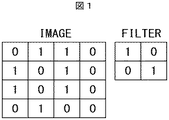
まず、CNNの畳み込み演算について図1、2A〜2Cを用いて説明する。図1は畳み込み演算の概念を説明する図であり、画像とフィルタを示す図である。図2A〜2Cは畳み込み演算の概念を説明する図であり、画像の画素値とフィルタの係数の積和演算を示す図である。 First, the CNN convolution operation will be described with reference to FIGS. FIG. 1 is a diagram for explaining the concept of convolution calculation, and shows an image and a filter. 2A to 2C are diagrams for explaining the concept of the convolution operation, and are diagrams illustrating the product-sum operation of the pixel value of the image and the coefficient of the filter.
説明を分かり易くするため、画像(IMAGE)を簡略化して数字で表すと高さ×幅の行列と考えることができる。図1の左に示すように、入力画像を例えば4×4の2値で表す。このような行列に、図1の右に示すように、2×2のフィルタ(FILTER)を適用し畳み込み演算する。 In order to make the explanation easy to understand, if the image (IMAGE) is simplified and represented by a number, it can be considered as a matrix of height × width. As shown on the left in FIG. 1, the input image is represented by binary values of 4 × 4, for example. As shown on the right side of FIG. 1, a 2 × 2 filter (FILTER) is applied to such a matrix to perform a convolution operation.
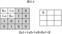
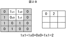
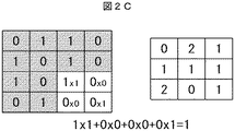
図2Aに示すように、画像の一番左上の部分にフィルタを重ね、同じ位置の値同士を掛け合わせる。掛け算の結果を足し合わせて出力する。図2Bに示すように、フィルタを1ピクセル分だけ横にずらして同じように値同士を掛け合せる。掛け算の結果を足し合わせて出力する。以下、図2Cに示すように、入力画像に対し、右下までフィルタ単位で要素ごとに掛け合わせて加算していく。 As shown in FIG. 2A, a filter is superimposed on the upper left portion of the image, and values at the same position are multiplied. The result of multiplication is added and output. As shown in FIG. 2B, the values are similarly multiplied by shifting the filter horizontally by one pixel. The result of multiplication is added and output. Hereinafter, as shown in FIG. 2C, the input image is multiplied and added element by element in the filter unit to the lower right.
畳み込み演算を行う場合、入力画像とフィルタの係数の畳み込み演算をチャネル数(フィルタの数)の分だけ繰り返す必要がある。 When performing the convolution operation, it is necessary to repeat the convolution operation of the input image and the filter coefficient by the number of channels (the number of filters).
実施形態では、チャネル別に累積加算する機能を備え、複数のチャネルを並行して畳み込み演算する。チャネル別に累積加算を実行可能なブロックの数と同等のチャネル数を同時に一括して畳み込み演算が可能なため、処理時間を短縮することができる。 In the embodiment, a function of cumulative addition for each channel is provided, and a plurality of channels are convolved in parallel. Since the number of channels equivalent to the number of blocks that can be cumulatively added for each channel can be simultaneously convolved, the processing time can be shortened.
畳み込み演算処理回路と統合係数テーブルを組み合わせて、複数のチャネルの畳み込み演算を1回で実施することができる。無駄な積和演算を省いてCNNを少ない積和演算回数で実現することができる。入力パタン生成回路を用いることで、フィルタサイズに依存せず、任意の畳み込み演算を実施することができる。 By combining the convolution operation processing circuit and the integrated coefficient table, convolution operations for a plurality of channels can be performed at one time. CNN can be realized with a small number of product-sum operations without useless product-sum operations. By using the input pattern generation circuit, any convolution operation can be performed without depending on the filter size.
以下、実施例および変形例について、図面を用いて説明する。ただし、以下の説明において、同一構成要素には同一符号を付し繰り返しの説明を省略することがある。 Hereinafter, examples and modifications will be described with reference to the drawings. However, in the following description, the same components may be denoted by the same reference numerals and repeated description may be omitted.
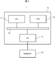
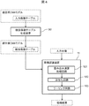
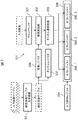
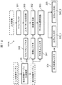
図3は画像認識システムの構成例を示すブロック図である。図4は図3の画像認識システムのデータの流れを示す図である。 FIG. 3 is a block diagram illustrating a configuration example of the image recognition system. FIG. 4 is a diagram showing a data flow of the image recognition system of FIG.
図3に示すように、画像認識システム1は半導体装置10と半導体記憶装置(MEMORY)20とを備える。半導体装置10は、画像認識装置(IRU)11と、中央処理装置(CPU)12と、半導体記憶装置20の制御回路(MC)13と、それらを接続するバス14と、を一つの半導体チップに備える。半導体記憶装置20は、例えばDDR−SDRAMである。
As shown in FIG. 3, the
図4に示すように、統合係数テーブル生成装置50は、記憶装置に格納された統合前CNNモデルに含まれる入力係数テーブルを統合し、統合後CNNモデルの統合係数テーブルを生成し、半導体記憶装置20に格納する。画像認識システム1の画像認識装置11は、半導体記憶装置20に格納された入力画像を統合係数テーブルに基づいて処理し、処理結果を半導体記憶装置20に格納する。
As shown in FIG. 4, the integrated coefficient
入力画像は、光学系(レンズ)や撮像素子を有する撮像装置(不図示)によって取得された画像であり、撮像装置が取得した画像の全体または一部である。入力画像は半導体記憶装置20に格納される。
The input image is an image acquired by an imaging device (not shown) having an optical system (lens) and an imaging device, and is the whole or a part of the image acquired by the imaging device. The input image is stored in the
画像認識装置11は、統合後CNNモデルの統合係数テーブルと入力画像を用いて計算し、処理結果を出力する。画像認識装置11は統合後CNNモデルで必要な演算を行う装置である。
The
処理結果は、画像認識装置11の出力であり、例えば入力画像の分類結果、セグメンテーション結果、特定物体の検知結果である。処理結果は半導体記憶装置20に格納される。
The processing result is an output of the
統合前CNNモデルは、一般的なCNNモデルを指す。例えば、AlexNet、VGGNet、SegNet、R−CNNである。入力係数テーブルは、結合前CNNモデルに含まれる係数のうち、畳み込み演算に用いられる係数である。 The pre-integration CNN model refers to a general CNN model. For example, AlexNet, VGGNet, SegNet, R-CNN. The input coefficient table is a coefficient used for the convolution operation among the coefficients included in the pre-combination CNN model.
統合係数テーブル生成装置50は、入力係数テーブルを分析し、より少ない畳み込み演算で処理可能な統合係数テーブルを生成する装置であり、例えば中央処理装置と中央処理装置のプログラム等を格納する記憶装置等で構成される。
The integrated coefficient
統合後CNNモデルは、統合前CNNモデルの畳み込み演算回数を削減したモデルである。統合係数テーブルは、統合係数テーブル生成装置50の出力である。
The post-integration CNN model is a model in which the number of convolution operations of the pre-integration CNN model is reduced. The integrated coefficient table is an output of the integrated coefficient
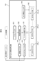
画像認識装置11は畳み込み演算処理回路101と活性化回路102とプーリング回路103とを備え、積演算結果をチャネル別に累積加算することが可能である。畳み込み演算処理回路101は、各係数に対応したチャネル番号ごとに畳み込み演算の結果を加算する。活性化回路102とプーリング回路103は、それぞれ活性化処理とプーリング処理を行う回路である。活性化処理には、例えば、周知のロジスティックジグモイド関数やReLU関数(Rectified Linear Units)などが用いられる。また、プーリング処理は、大きな画像を重要な情報は残しつつ縮小する方法で、例えば、画像内を小さなウィンドウに区切り、区切ったそれぞれのウィンドウから入力されるデータの最大値を出力する周知の最大プーリング関数や、入力されるデータの平均値を出力する周知の平均プーリング関数などが用いられる。
The
図5は畳み込み演算処理回路の構成例を説明するためのブロック図である。図6は図5のチャネル選択回路の構成例を説明するブロック図である。 FIG. 5 is a block diagram for explaining a configuration example of a convolution operation processing circuit. FIG. 6 is a block diagram illustrating a configuration example of the channel selection circuit of FIG.
統合係数テーブルは、畳み込み演算で用いられる係数が保存されているテーブルである。係数にチャネル番号が付加されている。統合係数テーブル生成装置50は複数の入力係数テーブルから統合係数テーブルを生成する。
The integrated coefficient table is a table in which coefficients used in the convolution calculation are stored. A channel number is added to the coefficient. The integrated coefficient
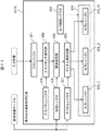
畳み込み演算処理回路101は、1回の畳み込み演算で複数回分の畳み込み演算の結果を出力する。畳み込み演算処理回路101は、ラインバッファ301と、積演算回路302と、チャネル選択回路303と、出力制御レジスタ304と、出力レジスタ305(第一出力レジスタ305_1、第二出力レジスタ305_2、・・・、第N出力レジスタ305_N)と、係数レジスタ306と、チャネルレジスタ307と、を備える。ラインバッファ301は指定されたライン数分の入力画像データを半導体記憶装置20より取得する。積演算回路302は、係数レジスタ306とラインバッファ301からの入力画像との積を計算する。チャネル選択回路303は、チャネルレジスタ307に登録されたチャネル番号を積演算結果に付加し、出力制御レジスタ304に従い、チャネル番号に応じて適切な出力レジスタ305に積演算結果を累積加算して出力する。出力制御レジスタ304は、チャネル番号と出力レジスタの番号を対応させる。
The convolution
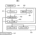
図6に示すように、チャネル選択回路303は、シフトダウン回路401、累積加算回路402、セレクタ回路403、累積加算レジスタ404を備えている。シフトダウン回路401は、積演算結果を指定されたビット数だけシフトダウンして出力する。累積加算回路402は、累積加算レジスタ404とシフトダウン回路401が出力した結果をチャネル番号ごとに加算して出力する。セレクタ回路403は、指定された出力レジスタ305に累積加算回路402の出力を出力する。
As shown in FIG. 6, the
出力制御レジスタ304、係数レジスタ306、チャネルレジスタ307はCPU12によって設定される。
The
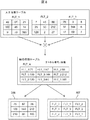
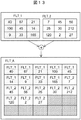
統合係数テーブル生成装置50が3種類の入力係数テーブルから1種の統合係数テーブルを生成し、その統合係数テーブルを用いて畳み込み演算する場合の例について図7〜10を用いて説明する。図7は3×3の畳み込み演算処理回路の構成を示すブロック図である。図8は図7の統合係数テーブル生成装置の動作を説明する模式図であり、3チャネル分の入力係数テーブルから1つの統合係数テーブルを生成する場合を示している。図9は図7の畳み込み演算処理回路の動作を説明する概念図である。図10は図7の累積加算回路の動作を説明する概念図である。
An example in which the integrated coefficient
図7の畳み込み演算処理回路は3×3畳み込み演算回路を用いて、3チャネル分の3×3畳み込み演算を1回で実行する。 The convolution operation processing circuit in FIG. 7 uses a 3 × 3 convolution operation circuit to execute 3 × 3 convolution operations for three channels at a time.
ここで、畳み込みに用いる係数テーブルの係数をwi,j,chanelとし、テーブルをCl,w,channelとし、 Here, the coefficient of the coefficient table used for convolution is w i, j, chanel , the table is C l, w, channel ,

とする。ただし、i,jは整数、channelがチャネル番号、lがテーブルの幅、wがテーブルの高さ、を表している。統合係数テーブルの係数を And Here, i and j are integers, channel is a channel number, l is a table width, and w is a table height. The coefficients of the integrated coefficient table
で表す。ただし、MAX(・・・)は引数のうち最大の値を返す関数である。 Represented by However, MAX (...) Is a function that returns the maximum value among the arguments.
また、li,j,FLT_Aを統合係数テーブルに用いるテーブルの種類を表す文字列とし、 Also, let l i, j, FLT_A be a character string representing the type of table used for the integration coefficient table,
とする。ただし、CHANNEL(・・・)は引数のうち最大の値を返したチャネル番号を表す関数である。このとき統合係数テーブルのC3,3,FLT_Aを And However, CHANNEL (...) Is a function representing the channel number that returned the maximum value among the arguments. At this time, C 3, 3, FLT_A of the integration coefficient table
と表す。 It expresses.
図8は具体的にl=3、w=3とした場合、どのように統合係数テーブルが生成されるかを模式的に表したものである。統合係数テーブル生成装置50は3種類の入力係数テーブル(FLT_1、FLT_2、FLT_3)を処理して統合係数テーブル(FLT_A)を出力する。入力係数テーブル(FLT_1、FLT_2、FLT_3)において、係数が一番大きいものが統合係数テーブルに出力されるが、その係数がそれぞれ網掛けされている。左上はFLT_3の「75」、中上はFLT_1の「87」、右上はFLT_2の「56」が最大値である。左中はFLT_1の「100」、中中はFLT_3の「144」、右中はFLT_2の「212」が最大値である。左下はFLT_2の「120」、中下はFLT_3の「60」、右下はFLT_1の「165」が最大値である。これらを統合した統合係数テーブル(FLT_A)には入力係数テーブル(FLT_1、FLT_2、FLT_3)のそれぞれの網掛け部分が配置される。統合係数テーブル(FLT_A)には係数の他にチャネル番号も格納される。
FIG. 8 schematically shows how the integrated coefficient table is generated when l = 3 and w = 3. The integrated coefficient
図8に示すように、畳み込み演算処理回路101は、統合係数テーブルから係数とチャネル番号を読み出し、それぞれ係数レジスタ306とチャネルレジスタ307に値を設定する。
As shown in FIG. 8, the convolution
図9に示すように、積演算回路302は係数レジスタ306に設定された値とラインバッファ301に設定された値の積を3×3の積演算回路で一度に計算する。チャネル選択回路303は、チャネルレジスタ307に設定された値(チャネル番号)に基づいて出力レジスタ305に累積加算回路402の出力を設定する。出力制御レジスタ304は出力レジスタ305とチャネルレジスタ307の対応を設定する。この例では、第一出力レジスタ305_1がFLT_1、第二出力レジスタ305_2がFLT_2、第三出力レジスタ305_3がFLT_3に対応する。畳み込み演算処理回路101は、第一出力レジスタ305_1、第二出力レジスタ305_2、第三出力レジスタ305_3にそれぞれFLT_1、FLT_2、FLT_3の係数を用いて畳み込み演算を実行した結果を出力する。
図10に示すように、累積加算回路402は、チャネルレジスタ307のチャネル番号に基づいて積演算回路302の演算結果と累積加算レジスタ404の内容をチャネル別に入力し各チャネルを並行して加算する。これにより、チャネル別の累積加算結果が一緒に得られる。畳み込み演算処理回路101は、積演算の結果を一律に累積加算するのではなく、チャネル番号によって別々に累積加算する。
As shown in FIG. 9, the
As shown in FIG. 10, the
具体例では、3×3畳み込み演算回路を用いて3チャネル分の3×3畳み込み演算を1回で実行する例を説明したが、これに限定されるものではなく、実施例はN×N畳み込み演算回路を用いてNチャネル分のN×N畳み込み演算を1回で実行することが可能である。 In the specific example, the 3 × 3 convolution operation circuit is used to execute the 3 × 3 convolution operation for 3 channels at a time. However, the embodiment is not limited to this, and the embodiment is not limited to N × N convolution. It is possible to execute N × N convolution calculations for N channels at a time using an arithmetic circuit.
<変形例>
以下、代表的な変形例について例示する。以下の変形例の説明において、上述の実施例にて説明されているものと同様の構成および機能を有する部分に対しては、上述の実施例と同様の符号が用いられ得るものとする。そして、かかる部分の説明については、技術的に矛盾しない範囲内において、上述の実施例における説明が適宜援用され得るものとする。また、上述の実施例の一部、および、変形例の全部または一部が、技術的に矛盾しない範囲内において、適宜、複合的に適用され得る。
<Modification>
Hereinafter, typical modifications will be illustrated. In the following description of the modified examples, the same reference numerals as those in the above-described embodiments can be used for portions having the same configurations and functions as those described in the above-described embodiments. And about description of this part, the description in the above-mentioned Example shall be used suitably in the range which is not technically consistent. In addition, a part of the above-described embodiments and all or a part of the modified examples can be appropriately combined in a range not technically inconsistent.
入力画像の配列によらず畳み込み演算を行う例について図11を用いて説明する。図11は畳み込み演算処理回路の他の構成例を説明するためのブロック図である。 An example of performing a convolution operation regardless of the arrangement of input images will be described with reference to FIG. FIG. 11 is a block diagram for explaining another configuration example of the convolution operation processing circuit.
畳み込み演算処理回路101Aは、実施例の畳み込み演算処理回路101の構成に、さらに入力パタンレジスタ308と入力パタン生成回路309を有する。入力パタンレジスタ308は、ラインバッファ301に設定された画素値をどのように入力パタン生成回路309から出力するかを設定するためのレジスタである。入力パタン生成回路309は、ラインバッファ301を入力とし、入力パタンレジスタ308に従った出力を生成する回路である。入力パタンレジスタ308はCPU12によって設定される。
The convolution
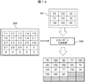
次に、統合係数テーブル生成装置50が2種類の入力係数テーブルから1種の統合係数テーブルを生成し、その統合係数テーブルを用いて畳み込み演算する場合の例について図12〜14を用いて説明する。図12は畳み込み演算処理回路の構成を示す図である。図13は図12の統合係数テーブル生成装置の動作を説明する模式図であり、2チャネル分の入力係数テーブルから1つの統合係数テーブルを生成する場合を示している。図14は図12の入力パタン生成回路の動作を説明する模式図であり、3×3入力画像を2チャネル分の5×5の入力画像を生成する場合を示している。
Next, an example in which the integrated coefficient
図12の畳み込み演算処理回路101Aは、5×5畳み込み演算回路を用いて、2回分の3×3畳み込み演算を1回で実行する。
The convolution
入力係数テーブルをC3,3,FLT_1、C3,3,FLT_2、統合係数テーブルをC5,5,FLT_A、とすると、 If the input coefficient table is C 3,3, FLT_1 , C 3,3, FLT_2 , and the integrated coefficient table is C 5,5, FLT_A ,
と表す。 It expresses.
また、Ii,jをi行j列の入力画像の画素値(濃淡値)、入力パタン生成回路309の出力をA5,5とし、
Also, I i, j is the pixel value (gray value) of the input image of i rows and j columns, and the output of the input
とする。 And
図13は具体的にl=3、w=3とした場合、どのように統合係数テーブルが生成されるかを模式的に表したものである。統合係数テーブル生成装置50は2種類の入力係数テーブル(FLT_1、FLT_2)を処理して統合係数テーブル(FLT_A)を出力する。3×3の入力係数テーブル(FLT_1、FLT_2)の係数を5×5の統合係数テーブルに出力される。
FIG. 13 schematically shows how the integrated coefficient table is generated when l = 3 and w = 3. The integrated coefficient
図13に示すように、FLT_Aの一行目の左から右にFLT_1の一行目の係数「40」、「87」、「21」、二行目の係数「100」、「45」が配置される。FLT_Aの二行目の左から右にFLT_1の二行目の右端の係数「14」、三行目の係数「9」、「33」、「165」、FLT_2の一行目の左端の係数「7」が配置される。FLT_Aの三行目の左から右にFLT_2の一行目の真ん中の係数「45」、右端の係数「56」、二行目の係数「25」、「30」、「212」が配置される。FLT_Aの四行目の左から右にFLT_2の三行目の係数「120」、「2」、「27」が配置される。FLT_Aの四行目の右の2か所およびFLT_Aの五行目には係数は配置されず、空欄となる。統合係数テーブル(FLT_A)には係数の他にチャネル番号も格納される。 As shown in FIG. 13, coefficients “40”, “87”, “21” in the first row of FLT — 1 and coefficients “100”, “45” in the second row are arranged from left to right in the first row of FLT_A. . From left to right of the second row of FLT_A, the coefficient “14” at the right end of the second row of FLT_1, the coefficients “9”, “33”, “165” of the third row, and the coefficient “7” of the left end of the first row of FLT_2 Is arranged. From the left to the right of the third row of FLT_A, the middle coefficient “45”, the rightmost coefficient “56” of the first row of FLT_2, and the coefficients “25”, “30”, and “212” of the second row are arranged. The coefficients “120”, “2”, and “27” in the third row of FLT_2 are arranged from left to right in the fourth row of FLT_A. Coefficients are not arranged in the two right places of the fourth row of FLT_A and the fifth row of FLT_A, and are blank. The integrated coefficient table (FLT_A) stores channel numbers in addition to coefficients.
図14に示すように、入力パタン生成回路309は、入力パタンレジスタ308の5×5の入力パタンに基づいてラインバッファ301より取得した3×3の画素を繰り返す形態で出力する。入力パタンは1回目の3×3の画素(1−1、1−2、・・・、1−9)と2回目の3×3の画素(2−1、2−2、・・・、2−9)の配置順番を規定する。
As shown in FIG. 14, the input
図14に示すように、入力パタン生成回路309の出力の一行目の左から右に入力画像の一行目の画素値「76」、「120」、「32」、二行目の画素値「77」、「130」が配置される。二行目の左から右に入力画像の二行目の右端の画素値「34」、三行目の画素値「130」、「100」、「54」、二回目の入力画像の一行目の左端の画素値「78」が配置される。三行目の左から右に入力画像の一行目の真ん中の画素値「120」、右端の画素値「32」、二行目の画素値「77」、「130」、「34」が配置される。四行目の左から右に入力画像の三行目の画素値「130」、「100」、「54」が配置される。四行目の右の2か所および五行目には画素は配置されず、空欄となる。これにより、入力パタン生成回路309の出力の画素の並びは統合係数テーブル(FLT_A)の係数の並びと同じである。
As shown in FIG. 14, the pixel values “76”, “120”, “32” of the first row of the input image from the left to the right of the first row of the output of the input
入力パタンレジスタ308および入力パタン生成回路309を追加することで、ラインバッファ301に格納されている画素を任意の形で読み出すことができる。
By adding the input pattern register 308 and the input
実施例と同様に、畳み込み演算処理回路101Aは、統合係数テーブルから係数とチャネル番号を読み出し、それぞれ係数レジスタ306とチャネルレジスタ307に値を設定する。
Similar to the embodiment, the convolution
実施例と同様に、積演算回路302は係数レジスタ306に設定された値と入力パタン生成回路309で生成された値の積を5×5の積演算回路で一度に計算する。チャネル選択回路303は、チャネルレジスタ307に設定された値(チャネル番号)に基づいて出力レジスタ305に累積加算回路402の出力を設定する。出力制御レジスタ304は出力レジスタ305とチャネルレジスタ307の対応を設定する。この例では、第一出力レジスタ305_1がFLT_1、第二出力レジスタ305_2がFLT_2に対応する。畳み込み演算処理回路101Aは、第一出力レジスタ305_1、第二出力レジスタ305_2、にそれぞれFLT_1、FLT_2の係数を用いて畳み込み演算を実行した結果を出力する。
実施例と同様に、累積加算回路402は、チャネルレジスタ307のチャネル番号に基づいて積演算回路の演算結果と累積加算レジスタの内容をチャネル別に入力し各チャネルを並行して加算する。これにより、チャネル別の累積加算結果が一緒に得られる。
Similar to the embodiment, the
Similar to the embodiment, the
変形例では、入力パタンレジスタ308と統合係数テーブル生成装置50を組み合わせて用いることで任意の畳み込み演算が実施可能となる。そのため、5×5の畳み込み演算回路を用いていても3×3や1×1の畳み込み演算を効率よく行うことが可能となる。
In the modification, an arbitrary convolution operation can be performed by using the input pattern register 308 and the integrated coefficient
具体例では、5×5畳み込み演算回路を用いて、2回分の3×3畳み込み演算を1回で実行する例について説明したが、これに限定されるものではなく、変形例はN×N畳み込み演算回路を用いて、L回分のM×M畳み込み演算を1回で実行することが可能である。ここで、M<N、L=INT(N2/M2)≧2である。 In the specific example, the example in which the 5 × 5 convolution operation circuit is used to execute 2 × 3 × 3 convolution operations at one time has been described. Using the arithmetic circuit, it is possible to execute L times of M × M convolution operations at one time. Here, M <N and L = INT (N 2 / M 2 ) ≧ 2.
以上、本発明者によってなされた発明を実施形態、実施例および変形例に基づき具体的に説明したが、本発明は、上記実施形態、実施例および変形例に限定されるものではなく、種々変更可能であることはいうまでもない。 As mentioned above, the invention made by the present inventor has been specifically described based on the embodiments, examples, and modifications. However, the present invention is not limited to the above-described embodiments, examples, and modifications, and various modifications can be made. It goes without saying that it is possible.
1・・・画像認識システム
10・・・半導体装置
11・・・画像認識装置
101・・・畳み込み演算処理回路
301・・・ラインバッファ
302・・・積演算回路
303・・・チャネル選択回路
401・・・シフトダウン回路
402・・・累積加算回路
403・・・セレクタ回路
404・・・累積加算レジスタ
304・・・出力制御回路
305・・・出力レジスタ
306・・・係数レジスタ
307・・・チャネルレジスタ
308・・・入力パタンレジスタ
309・・・入力パタン生成回路
102・・・活性化回路
103・・・プーリング回路
12・・・中央処理装置
13・・・制御回路
14・・・バス
20・・・半導体記憶装置
50・・・統合係数テーブル生成装置
DESCRIPTION OF
Claims (18)
前記畳み込み演算処理回路は、
統合係数テーブルの係数が設定される係数レジスタと、
入力画像と前記係数との積を求める積演算回路と、
前記統合係数テーブルのチャネル番号が設定されるチャネルレジスタと、
前記チャネル番号に基づいて累積加算演算の出力先を選択するチャネル選択回路と、
前記累積加算演算の結果を格納する複数の出力レジスタと、
を備え、
前記統合係数テーブルは複数の入力係数テーブルを統合したものであり、前記統合係数テーブルはN×Nの大きさであり、
前記積演算回路はN×Nのデータを一度に演算することが可能な半導体装置。 An image recognition device having a convolution operation processing circuit is provided,
The convolution processing circuit is
A coefficient register in which the coefficients of the integrated coefficient table are set;
A product operation circuit for obtaining a product of the input image and the coefficient;
A channel register in which a channel number of the integration coefficient table is set;
A channel selection circuit that selects an output destination of the cumulative addition operation based on the channel number;
A plurality of output registers for storing the result of the cumulative addition operation;
With
The integrated coefficient table is obtained by integrating a plurality of input coefficient tables, and the integrated coefficient table has a size of N × N,
The product operation circuit is a semiconductor device capable of calculating N × N data at a time.
前記チャネル選択回路は、
前記チャネル番号ごとに前記積を加算する累積加算回路と、
前記累積加算回路の出力を前記チャネル番号ごとに保持する累積加算レジスタと、
を備え、
前記累積加算回路は、前記チャネル番号ごとの加算を並行して行う半導体装置。 In claim 1,
The channel selection circuit includes:
A cumulative addition circuit for adding the product for each channel number;
A cumulative addition register for holding the output of the cumulative addition circuit for each channel number;
With
The cumulative addition circuit is a semiconductor device that performs addition for each channel number in parallel.
前記チャネル選択回路は、さらに、前記チャネル番号に基づいて前記累積加算回路の出力を前記複数の出力レジスタのいずれかに出力するセレクタを備える半導体装置。 In claim 2,
The channel selection circuit further includes a selector that outputs an output of the cumulative addition circuit to any one of the plurality of output registers based on the channel number.
前記統合係数テーブルの各要素は前記複数の入力係数テーブルの対応する各要素において最も大きい値の係数が格納される半導体装置。 In claim 1,
Each element of the integrated coefficient table is a semiconductor device in which a coefficient having the largest value is stored in each corresponding element of the plurality of input coefficient tables.
前記複数の入力係数テーブルの個数はN個であり、前記複数の入力係数テーブルのそれぞれはN×Nの大きさである半導体装置。 In claim 1,
The number of the plurality of input coefficient tables is N, and each of the plurality of input coefficient tables is a size of N × N.
入力パタンレジスタと、
前記入力パタンレジスタの内容に基づいて入力画像の配置を変更する入力パタン生成回路と、
を備え、
前記統合係数テーブルはL個の入力係数テーブルを統合したものであり、前記統合係数テーブルはN×Nの大きさであり、前記L個の入力係数テーブルのそれぞれはM×Mの大きさであり、MはNよりも小さい値であり、
前記積演算回路はN×Nのデータを一度に演算することが可能な半導体装置。 The input pattern register according to claim 1, further comprising:
An input pattern generation circuit for changing the arrangement of the input image based on the contents of the input pattern register;
With
The integrated coefficient table is obtained by integrating L input coefficient tables, and the integrated coefficient table has a size of N × N, and each of the L input coefficient tables has a size of M × M. , M is a value smaller than N,
The product operation circuit is a semiconductor device capable of calculating N × N data at a time.
前記チャネル選択回路は、
前記チャネル番号ごとに前記積を加算する累積加算回路と、
前記累積加算回路の出力を前記チャネル番号ごとに保持する累積加算レジスタと、
を備え、
前記累積加算回路は、前記チャネル番号ごとの加算を並行して行う半導体装置。 In claim 6,
The channel selection circuit includes:
A cumulative addition circuit for adding the product for each channel number;
A cumulative addition register for holding the output of the cumulative addition circuit for each channel number;
With
The cumulative addition circuit is a semiconductor device that performs addition for each channel number in parallel.
前記チャネル選択回路は、さらに、前記チャネル番号に基づいて前記累積加算回路の出力を前記複数の出力レジスタのいずれかに出力するセレクタを備える半導体装置。 In claim 7,
The channel selection circuit further includes a selector that outputs an output of the cumulative addition circuit to any one of the plurality of output registers based on the channel number.
前記入力パタン生成回路は、M×Mの入力画像を前記L個繰り返してN×Nの入力画像に変換する半導体装置。 In claim 6,
The input pattern generation circuit is a semiconductor device that repeats the L number of M × M input images into an N × N input image.
半導体記憶装置と、
を備え、
前記半導体装置は、
統合係数テーブルの係数が設定される係数レジスタと、前記半導体記憶装置から読み出した入力画像と前記係数との積を求める積演算回路と、前記統合係数テーブルのチャネル番号が設定されるチャネルレジスタと、前記チャネル番号に基づいて累積加算演算の出力先を選択するチャネル選択回路と、前記累積加算演算の結果を格納する複数の出力レジスタと、を有する畳み込み演算処理回路と、
プーリング回路と、
を備え、
前記積演算回路はN×Nのデータを一度に演算することが可能であり、
前記統合係数テーブルは複数の入力係数テーブルを統合したものであり、前記統合係数テーブルはN×Nの大きさである画像認識システム。 A semiconductor device;
A semiconductor memory device;
With
The semiconductor device includes:
A coefficient register in which coefficients of the integrated coefficient table are set; a product operation circuit for obtaining a product of the input image read from the semiconductor storage device and the coefficients; a channel register in which channel numbers of the integrated coefficient table are set; A convolution operation processing circuit comprising: a channel selection circuit that selects an output destination of the cumulative addition operation based on the channel number; and a plurality of output registers that store the result of the cumulative addition operation;
A pooling circuit;
With
The product operation circuit can calculate N × N data at a time,
The integrated coefficient table is an image recognition system in which a plurality of input coefficient tables are integrated, and the integrated coefficient table has a size of N × N.
前記チャネル選択回路は、
前記チャネル番号ごとに前記積を加算する累積加算回路と、
前記累積加算回路の出力を前記チャネル番号ごとに保持する累積加算レジスタと、
を備え、
前記累積加算回路は、前記チャネル番号ごとの加算を並行して行う画像認識システム。 In claim 10,
The channel selection circuit includes:
A cumulative addition circuit for adding the product for each channel number;
A cumulative addition register for holding the output of the cumulative addition circuit for each channel number;
With
The cumulative addition circuit is an image recognition system that performs addition for each channel number in parallel.
前記チャネル選択回路は、さらに、前記チャネル番号に基づいて前記累積加算回路の出力を前記複数の出力レジスタのいずれかに出力するセレクタを備える画像認識システム。 In claim 11,
The channel selection circuit further includes a selector that outputs an output of the cumulative addition circuit to any one of the plurality of output registers based on the channel number.
前記統合係数テーブルの各要素は前記複数の入力係数テーブルの対応する各要素において最も大きい値の係数が格納される画像認識システム。 In claim 10,
The image recognition system in which each element of the integrated coefficient table stores a coefficient having the largest value in each corresponding element of the plurality of input coefficient tables.
前記複数の入力係数テーブルの個数はN個であり、前記複数の入力係数テーブルのそれぞれはN×Nの大きさである画像認識システム。 In claim 10,
The number of the plurality of input coefficient tables is N, and each of the plurality of input coefficient tables has a size of N × N.
前記半導体装置は、さらに、
入力パタンレジスタと、
前記入力パタンレジスタの内容に基づいて入力画像の配置を変更する入力パタン生成回路と、
を備え、
前記統合係数テーブルはL個の入力係数テーブルを統合したものであり、前記統合係数テーブルはN×Nの大きさであり、前記L個の入力係数テーブルのそれぞれはM×Mの大きさであり、MはNよりも小さい値であり、
前記積演算回路はN×Nのデータを一度に演算することが可能な画像認識システム。 In claim 10,
The semiconductor device further includes:
An input pattern register;
An input pattern generation circuit for changing the arrangement of the input image based on the contents of the input pattern register;
With
The integrated coefficient table is obtained by integrating L input coefficient tables, and the integrated coefficient table has a size of N × N, and each of the L input coefficient tables has a size of M × M. , M is a value smaller than N,
The product calculation circuit is an image recognition system capable of calculating N × N data at a time.
前記チャネル選択回路は、
前記チャネル番号ごとに前記積を加算する累積加算回路と、
前記累積加算回路の出力を前記チャネル番号ごとに保持する累積加算レジスタと、
を備え、
前記累積加算回路は、前記チャネル番号ごとの加算を並行して行う画像認識システム。 In claim 15,
The channel selection circuit includes:
A cumulative addition circuit for adding the product for each channel number;
A cumulative addition register for holding the output of the cumulative addition circuit for each channel number;
With
The cumulative addition circuit is an image recognition system that performs addition for each channel number in parallel.
前記チャネル選択回路は、さらに、前記チャネル番号に基づいて前記累積加算回路の出力を前記複数の出力レジスタのいずれかに出力するセレクタを備える画像認識システム。 In claim 16,
The channel selection circuit further includes a selector that outputs an output of the cumulative addition circuit to any one of the plurality of output registers based on the channel number.
前記入力パタン生成回路は、M×Mの入力画像を前記L個繰り返してN×Nの入力画像に変換する画像認識システム。 In claim 15,
The input pattern generation circuit is an image recognition system that repeats the L number of M × M input images into an N × N input image.
Priority Applications (5)
| Application Number | Priority Date | Filing Date | Title |
|---|---|---|---|
| JP2017162057A JP2019040403A (en) | 2017-08-25 | 2017-08-25 | Semiconductor device and image recognition system |
| US16/035,010 US11461633B2 (en) | 2017-08-25 | 2018-07-13 | Semiconductor device and image recognition system |
| EP18185295.5A EP3447682B1 (en) | 2017-08-25 | 2018-07-24 | Semiconductor device and image recognition system |
| TW107126993A TW201921287A (en) | 2017-08-25 | 2018-08-03 | Semiconductor device and image recognition system |
| CN201810938920.6A CN109427035B (en) | 2017-08-25 | 2018-08-17 | Semiconductor device and image recognition system |
Applications Claiming Priority (1)
| Application Number | Priority Date | Filing Date | Title |
|---|---|---|---|
| JP2017162057A JP2019040403A (en) | 2017-08-25 | 2017-08-25 | Semiconductor device and image recognition system |
Publications (1)
| Publication Number | Publication Date |
|---|---|
| JP2019040403A true JP2019040403A (en) | 2019-03-14 |
Family
ID=63041921
Family Applications (1)
| Application Number | Title | Priority Date | Filing Date |
|---|---|---|---|
| JP2017162057A Pending JP2019040403A (en) | 2017-08-25 | 2017-08-25 | Semiconductor device and image recognition system |
Country Status (5)
| Country | Link |
|---|---|
| US (1) | US11461633B2 (en) |
| EP (1) | EP3447682B1 (en) |
| JP (1) | JP2019040403A (en) |
| CN (1) | CN109427035B (en) |
| TW (1) | TW201921287A (en) |
Cited By (3)
| Publication number | Priority date | Publication date | Assignee | Title |
|---|---|---|---|---|
| EP4102411A1 (en) | 2021-06-11 | 2022-12-14 | Renesas Electronics Corporation | Semiconductor device |
| DE102022212269A1 (en) | 2021-11-22 | 2023-05-25 | Renesas Electronics Corporation | SEMICONDUCTOR DEVICE |
| DE102023204651A1 (en) | 2022-05-18 | 2023-11-23 | Renesas Electronics Corporation | SEMICONDUCTOR DEVICE |
Family Cites Families (8)
| Publication number | Priority date | Publication date | Assignee | Title |
|---|---|---|---|---|
| AUPQ289099A0 (en) * | 1999-09-16 | 1999-10-07 | Silverbrook Research Pty Ltd | Method and apparatus for manipulating a bayer image |
| JP5184824B2 (en) | 2007-06-15 | 2013-04-17 | キヤノン株式会社 | Arithmetic processing apparatus and method |
| JP5376920B2 (en) | 2008-12-04 | 2013-12-25 | キヤノン株式会社 | Convolution operation circuit, hierarchical convolution operation circuit, and object recognition device |
| JP6365258B2 (en) | 2014-11-19 | 2018-08-01 | 株式会社デンソー | Arithmetic processing unit |
| US9582726B2 (en) * | 2015-06-24 | 2017-02-28 | Qualcomm Incorporated | Systems and methods for image processing in a deep convolution network |
| JP6700712B2 (en) | 2015-10-21 | 2020-05-27 | キヤノン株式会社 | Convolution operation device |
| CN108073549B (en) * | 2016-11-14 | 2021-04-27 | 耐能股份有限公司 | Convolution operation device and method |
| CN106951395B (en) * | 2017-02-13 | 2018-08-17 | 上海客鹭信息技术有限公司 | Parallel convolution operations method and device towards compression convolutional neural networks |
-
2017
- 2017-08-25 JP JP2017162057A patent/JP2019040403A/en active Pending
-
2018
- 2018-07-13 US US16/035,010 patent/US11461633B2/en active Active
- 2018-07-24 EP EP18185295.5A patent/EP3447682B1/en active Active
- 2018-08-03 TW TW107126993A patent/TW201921287A/en unknown
- 2018-08-17 CN CN201810938920.6A patent/CN109427035B/en active Active
Cited By (4)
| Publication number | Priority date | Publication date | Assignee | Title |
|---|---|---|---|---|
| EP4102411A1 (en) | 2021-06-11 | 2022-12-14 | Renesas Electronics Corporation | Semiconductor device |
| DE102022212269A1 (en) | 2021-11-22 | 2023-05-25 | Renesas Electronics Corporation | SEMICONDUCTOR DEVICE |
| KR20230075349A (en) | 2021-11-22 | 2023-05-31 | 르네사스 일렉트로닉스 가부시키가이샤 | Semiconductor device |
| DE102023204651A1 (en) | 2022-05-18 | 2023-11-23 | Renesas Electronics Corporation | SEMICONDUCTOR DEVICE |
Also Published As
| Publication number | Publication date |
|---|---|
| CN109427035B (en) | 2023-09-05 |
| EP3447682A1 (en) | 2019-02-27 |
| US11461633B2 (en) | 2022-10-04 |
| EP3447682B1 (en) | 2023-05-24 |
| TW201921287A (en) | 2019-06-01 |
| US20190065947A1 (en) | 2019-02-28 |
| CN109427035A (en) | 2019-03-05 |
Similar Documents
| Publication | Publication Date | Title |
|---|---|---|
| JP6945986B2 (en) | Arithmetic circuit, its control method and program | |
| CN108133270B (en) | Convolutional neural network acceleration method and device | |
| US10824934B2 (en) | Methods and apparatus for matrix processing in a convolutional neural network | |
| JP6700712B2 (en) | Convolution operation device | |
| JP2018067154A (en) | Arithmetic processing circuit and recognition system | |
| US11487845B2 (en) | Convolutional operation device with dimensional conversion | |
| JP2019040403A (en) | Semiconductor device and image recognition system | |
| EP3093757B1 (en) | Multi-dimensional sliding window operation for a vector processor | |
| CN108717571B (en) | Acceleration method and device for artificial intelligence | |
| CN111738433B (en) | Reconfigurable convolution hardware accelerator | |
| CN108073549B (en) | Convolution operation device and method | |
| CN108681773B (en) | Data operation acceleration method, device, terminal and readable storage medium | |
| WO2022121474A1 (en) | Method and system for optimizing convolutional residual structure of neural network, device, and medium | |
| JP2018073103A (en) | Arithmetic circuit, method for controlling the same, and program | |
| JP6532334B2 (en) | Parallel computing device, image processing device and parallel computing method | |
| CN110738317A (en) | FPGA-based deformable convolution network operation method, device and system | |
| US20170278214A1 (en) | Image processing apparatus, image processing method, and vehicle control apparatus | |
| US20220101083A1 (en) | Methods and apparatus for matrix processing in a convolutional neural network | |
| CN113657587A (en) | FPGA-based deformable convolution acceleration method and device | |
| CN112099737B (en) | Method, device, equipment and storage medium for storing data | |
| WO2023112581A1 (en) | Inference device | |
| US20220004363A1 (en) | Semiconductor device, data generation methods used for the same, and method of controlling the same | |
| KR102428033B1 (en) | Hardware accelerator for transposed convolution operation | |
| JP2018195060A (en) | Arithmetic processing device | |
| KR20230059726A (en) | Method and electronic device for performing deep neural network operations |