JP2018534847A - Multi-lane N-factorial coding communication system and other multi-wire communication systems - Google Patents
Multi-lane N-factorial coding communication system and other multi-wire communication systems Download PDFInfo
- Publication number
- JP2018534847A JP2018534847A JP2018517310A JP2018517310A JP2018534847A JP 2018534847 A JP2018534847 A JP 2018534847A JP 2018517310 A JP2018517310 A JP 2018517310A JP 2018517310 A JP2018517310 A JP 2018517310A JP 2018534847 A JP2018534847 A JP 2018534847A
- Authority
- JP
- Japan
- Prior art keywords
- symbols
- sequence
- clock signal
- clock
- symbol
- Prior art date
- Legal status (The legal status is an assumption and is not a legal conclusion. Google has not performed a legal analysis and makes no representation as to the accuracy of the status listed.)
- Pending
Links
Images


Classifications
-
- H—ELECTRICITY
- H04—ELECTRIC COMMUNICATION TECHNIQUE
- H04L—TRANSMISSION OF DIGITAL INFORMATION, e.g. TELEGRAPHIC COMMUNICATION
- H04L7/00—Arrangements for synchronising receiver with transmitter
- H04L7/0008—Synchronisation information channels, e.g. clock distribution lines
-
- G—PHYSICS
- G06—COMPUTING; CALCULATING OR COUNTING
- G06F—ELECTRIC DIGITAL DATA PROCESSING
- G06F13/00—Interconnection of, or transfer of information or other signals between, memories, input/output devices or central processing units
- G06F13/38—Information transfer, e.g. on bus
- G06F13/42—Bus transfer protocol, e.g. handshake; Synchronisation
- G06F13/4282—Bus transfer protocol, e.g. handshake; Synchronisation on a serial bus, e.g. I2C bus, SPI bus
- G06F13/4291—Bus transfer protocol, e.g. handshake; Synchronisation on a serial bus, e.g. I2C bus, SPI bus using a clocked protocol
-
- H—ELECTRICITY
- H04—ELECTRIC COMMUNICATION TECHNIQUE
- H04L—TRANSMISSION OF DIGITAL INFORMATION, e.g. TELEGRAPHIC COMMUNICATION
- H04L25/00—Baseband systems
- H04L25/02—Details ; arrangements for supplying electrical power along data transmission lines
- H04L25/14—Channel dividing arrangements, i.e. in which a single bit stream is divided between several baseband channels and reassembled at the receiver
-
- H—ELECTRICITY
- H04—ELECTRIC COMMUNICATION TECHNIQUE
- H04L—TRANSMISSION OF DIGITAL INFORMATION, e.g. TELEGRAPHIC COMMUNICATION
- H04L25/00—Baseband systems
- H04L25/38—Synchronous or start-stop systems, e.g. for Baudot code
- H04L25/40—Transmitting circuits; Receiving circuits
- H04L25/49—Transmitting circuits; Receiving circuits using code conversion at the transmitter; using predistortion; using insertion of idle bits for obtaining a desired frequency spectrum; using three or more amplitude levels ; Baseband coding techniques specific to data transmission systems
Abstract
特に電子装置内の2つのデバイス間の、マルチワイヤデータ通信リンクを通じたデータの通信を容易にする、システム、方法、および装置が説明される。受信デバイスは、マルチワイヤリンクを通じてシンボルのシーケンスを受信する。受信デバイスはさらに、専用クロック線を介してクロック信号を受信し、専用クロック線は、マルチワイヤリンクとは別個であり並列である。受信デバイスは、クロック信号を使用してシンボルのシーケンスを復号する。ある態様では、第2のクロック信号が、シンボルのシーケンスの中の連続するシンボルのペアとペアの間の保証された遷移に埋め込まれる。したがって、受信デバイスは、第2のクロック信号を無視する一方、専用クロック線を介して受信されるクロック信号を使用して、シンボルのシーケンスを復号する。 Systems, methods, and apparatus are described that facilitate communication of data over a multi-wire data communication link, particularly between two devices in an electronic device. A receiving device receives a sequence of symbols over a multi-wire link. The receiving device further receives a clock signal via a dedicated clock line, which is separate and parallel to the multi-wire link. The receiving device uses the clock signal to decode the sequence of symbols. In an aspect, the second clock signal is embedded in a guaranteed transition between pairs of consecutive symbols in the sequence of symbols. Thus, the receiving device ignores the second clock signal while using the clock signal received via the dedicated clock line to decode the sequence of symbols.
Description
関連出願の相互参照
[0001]本出願は、2015年10月5日に米国特許商標庁に出願された非仮出願第14/875,592号の優先権と利益とを主張し、この非仮出願は、2014年4月10日に出願された「Multi−Lane N−Factorial (N!) And Other Multi−Wire Communication Systems」という表題の米国非仮出願第14/250,119号の一部継続出願であり、2013年10月3日に出願された「N Factorial Clock And Data Recovery With Negative Hold Time Sampling」という表題の米国仮出願第61/886,567号の優先権を主張する2014年4月14日に出願された「N Factorial Dual Data Rate Clock And Data Recovery」という表題の米国非仮出願第14/252,450号の一部継続出願でもあり、さらに、2013年10月3日に出願された「Method To Enhance MIPI D−PHY Link Rate With Minimal PHY Changes And No Protocol Changes」という表題の米国仮出願第61/886,556号の優先権を主張する2014年9月19日に出願された「Method To Enhance MIPI D−PHY Link Rate With Minimal PHY Changes And No Protocol Changes」という表題の米国非仮出願第14/491,884号の一部継続出願であり、これらの内容全体が参考として本明細書に組み込まれる。
Cross-reference of related applications
[0001] This application claims the priority and benefit of non-provisional application No. 14 / 875,592, filed with the US Patent and Trademark Office on October 5, 2015, which non-provisional application is This is a continuation-in-part application of US Non-Provisional Application No. 14 / 250,119 entitled “Multi-Lane N-Factorial (N!) And Other Multi-Wire Communication Systems” filed on April 10, 2013. Filed on Apr. 14, 2014 claiming priority of US Provisional Application No. 61 / 886,567 entitled “N Factory Clock And Data Recovery With Negative Hold Time Sampling” filed Oct. 3, “N Factory Dual Dat It is also a continuation-in-part of US Non-Provisional Application No. 14 / 252,450 entitled “Rate Clock And Data Recovery”, and further, “Method To Enhancement MIPI D-PHY Link Rate” filed on October 3, 2013. “Method To Enhancing MIPI D-PHY Link Rate Rate” filed on September 19, 2014 claiming priority from US Provisional Application No. 61 / 886,556 entitled “With Minimal PHY Changes And No Protocol Changes”. This is a continuation-in-part of US Non-Provisional Application No. 14 / 491,884 entitled “PHY Changes And No Protocol Changes” Is incorporated herein by reference.
[0002]本開示は全般にデータ通信インターフェースに関し、より具体的には、マルチレーンのマルチワイヤデータ通信インターフェースに関する。 [0002] This disclosure relates generally to data communication interfaces, and more specifically to multi-lane multi-wire data communication interfaces.
[0003]携帯電話などのモバイルデバイスの製造業者は、異なる製造業者を含む様々な供給源からモバイルデバイスの部品を入手することがある。たとえば、携帯電話の中のアプリケーションプロセッサは第1の製造業者から入手され得るが、携帯電話のディスプレイは第2の製造業者から入手され得る。アプリケーションプロセッサおよびディスプレイまたは他のデバイスは、規格に基づいた、またはプロプライエタリな物理インターフェースを使用して相互接続され得る。たとえば、ディスプレイは、Mobile Industry Processor Interface Alliance(MIPI)によって指定されるDisplay System Interface(DSI)規格に準拠するインターフェースを提供し得る。 [0003] Manufacturers of mobile devices such as cell phones may obtain mobile device parts from various sources, including different manufacturers. For example, the application processor in a mobile phone can be obtained from a first manufacturer, while the display of the mobile phone can be obtained from a second manufacturer. Application processors and displays or other devices may be interconnected using standard-based or proprietary physical interfaces. For example, the display may provide an interface that conforms to the Display System Interface (DSI) standard specified by the Mobile Industry Processor Interface Alliance (MIPI).
[0004]一例では、マルチシグナルデータ転送システムは、3相またはN階乗(N!)低電圧差動シグナリング(LVDS)などのマルチワイヤ差動シグナリングを利用することがあり、一つ一つのシンボルサイクルにおいてシンボル遷移を引き起こすことによってシンボルクロック情報を埋め込むために、トランスコーディング(たとえば、ある符号化タイプから別の符号化タイプへのデジタル対デジタルのデータ変換)が実行されることがある。トランスコーディングによってクロック情報を埋め込むことは、クロックとデータ信号との間のスキューを最小にするための、ならびに、データ信号からクロック情報を復元するための位相ロックループ(PLL)の必要性をなくすための、効果的な方法である。 [0004] In one example, a multi-signal data transfer system may utilize multi-wire differential signaling, such as three-phase or N-factorial (N!) Low voltage differential signaling (LVDS), and each symbol Transcoding (eg, digital-to-digital data conversion from one encoding type to another encoding type) may be performed to embed symbol clock information by causing symbol transitions in a cycle. Embedding clock information by transcoding minimizes the skew between the clock and the data signal, as well as eliminates the need for a phase locked loop (PLL) to recover the clock information from the data signal. It is an effective method.
[0005]マルチシグナル通信リンク上での最適化された通信および改善されたデータ転送レートに対する、継続的な需要が存在する。 [0005] There is a continuing demand for optimized communication and improved data transfer rates over multi-signal communication links.
[0006]本明細書において開示される実施形態は、マルチレーンのマルチワイヤインターフェースに関するシステムと、方法と、装置とを提供する。 [0006] Embodiments disclosed herein provide systems, methods, and apparatus for multi-lane, multi-wire interfaces.
[0007]本開示のある態様では、受信デバイスにおけるデータ通信の方法は、マルチワイヤリンクを通じてシンボルのシーケンスを受信することを含む。シンボルのシーケンスの中の各シンボルは、マルチワイヤリンクのN本のワイヤのシグナリング状態に対応し、ここでNは1より大きい整数である。方法はさらに、専用クロック線を介してクロック信号を受信することと、ここにおいて、専用クロック線が、マルチワイヤリンクとは別個であり並列である、クロック信号を使用してシンボルのシーケンスを復号することとを含む。 [0007] In certain aspects of the present disclosure, a method of data communication at a receiving device includes receiving a sequence of symbols over a multi-wire link. Each symbol in the sequence of symbols corresponds to the signaling state of N wires of the multi-wire link, where N is an integer greater than one. The method further includes receiving a clock signal via a dedicated clock line, wherein the dedicated clock line is separate and parallel to the multi-wire link and uses the clock signal to decode a sequence of symbols. Including.
[0008]本開示のある態様では、第2のクロック信号が、シンボルのシーケンスの中の連続するシンボルのペアとペアの間の保証された遷移に埋め込まれる。したがって、方法は、第2のクロック信号を無視する一方、専用クロック線を介して受信されるクロック信号を使用して、シンボルのシーケンスを復号する。 [0008] In certain aspects of the present disclosure, a second clock signal is embedded in a guaranteed transition between pairs of consecutive symbols in a sequence of symbols. Thus, the method decodes the sequence of symbols using the clock signal received via the dedicated clock line while ignoring the second clock signal.
[0009]本開示のある態様では、復号することは、クロック信号を使用してシンボルのシーケンスをデータビットのセットに変換することを含む。本開示のさらなる態様では、シンボルのシーケンスをデータビットのセットに変換することは、シンボルのシーケンスを遷移数のセットに変換するためにトランスコーダを使用することと、遷移数のセットをデータビットのセットに変換することとを含む。 [0009] In certain aspects of the present disclosure, decoding includes converting a sequence of symbols into a set of data bits using a clock signal. In a further aspect of the disclosure, converting the sequence of symbols into a set of data bits includes using a transcoder to convert the sequence of symbols into a set of transition numbers, and converting the set of transition numbers into a set of data bits. Converting to a set.
[0010]本開示のある態様では、マルチワイヤリンクのうちの少なくとも1本の線は双方向性である。方法はさらに、専用クロック線を介して受信されたクロック信号に基づいて、少なくとも1つの双方向の線を通じてシンボルの第2のシーケンスを送信することを含む。 [0010] In certain aspects of the present disclosure, at least one line of the multi-wire link is bidirectional. The method further includes transmitting a second sequence of symbols over at least one bi-directional line based on a clock signal received via the dedicated clock line.
[0011]本開示のある態様では、専用クロック線は、双方向性であり、マルチワイヤリンクを通じて送信するあらゆるデバイスから駆動され得る。方法はさらに、専用クロック線を介して第3のクロック信号を送信することを含む。第3のクロック信号は、少なくとも1つの双方向の線を通じて送信されるシンボルのシーケンスへとデータビットを符号化するために使用される送信クロックと関連付けられ得る。 [0011] In certain aspects of the present disclosure, the dedicated clock line is bidirectional and can be driven from any device transmitting over a multi-wire link. The method further includes transmitting a third clock signal via a dedicated clock line. The third clock signal may be associated with a transmit clock used to encode the data bits into a sequence of symbols transmitted over at least one bi-directional line.
[0012]本開示のある態様では、受信デバイスは処理回路を含む。メモリが処理回路に結合され得る。処理回路は、マルチワイヤリンクを通じてシンボルのシーケンスを受信し、専用クロック線を介してクロック信号を受信し、ここにおいて、専用クロック線が、マルチワイヤリンクとは別個であり並列である、クロック信号を使用してシンボルのシーケンスを復号するように構成される。 [0012] In certain aspects of the present disclosure, the receiving device includes processing circuitry. A memory may be coupled to the processing circuit. The processing circuit receives a sequence of symbols over a multi-wire link and receives a clock signal over a dedicated clock line, where the dedicated clock line is separate from and parallel to the multi-wire link. And configured to decode a sequence of symbols.
[0013]本開示のある態様では、装置は、マルチワイヤリンクを通じてシンボルのシーケンスを受信するための手段と、専用クロック線を介してクロック信号を受信するための手段と、ここにおいて、専用クロック線が、マルチワイヤリンクとは別個であり並列である、クロック信号を使用してシンボルのシーケンスを復号するための手段とを含む。 [0013] In certain aspects of the present disclosure, an apparatus includes: means for receiving a sequence of symbols over a multi-wire link; means for receiving a clock signal via a dedicated clock line; Includes means for decoding a sequence of symbols using a clock signal that is separate and parallel to the multi-wire link.
[0014]本開示のある態様では、プロセッサ可読記憶媒体は、1つまたは複数の命令を記憶または維持している。少なくとも1つの処理回路によって実行されると、命令は、少なくとも1つの処理回路に、マルチワイヤリンクを通じてシンボルのシーケンスを受信させ、専用クロック線を介してクロック信号を受信させ、ここにおいて、専用クロック線が、マルチワイヤリンクとは別個であり並列である、クロック信号を使用してシンボルのシーケンスを復号させる。 [0014] In certain aspects of the present disclosure, a processor-readable storage medium stores or maintains one or more instructions. When executed by at least one processing circuit, the instructions cause at least one processing circuit to receive a sequence of symbols over a multi-wire link and receive a clock signal over a dedicated clock line, where the dedicated clock line However, a sequence of symbols is decoded using a clock signal that is separate and parallel to the multi-wire link.
[0015]本開示のある態様では、送信デバイスにおけるデータ通信の方法は、データビットをシンボルのシーケンスへと符号化することと、任意選択でシンボルのシーケンスに第2のクロック信号を埋め込むこととを含み、ここにおいて、第2のクロック信号は、シンボルのシーケンスの中の連続するシンボルのペアとペアの間の保証された遷移に埋め込まれる。シンボルのシーケンスの中の各シンボルは、マルチワイヤリンクのN本のワイヤのシグナリング状態に対応し、ここでNは1より大きい整数である。方法はさらに、マルチワイヤリンクを通じてシンボルのシーケンスを送信することと、専用クロック線を介してシンボルのシーケンスと関連付けられるクロック信号を送信することとを含み、ここにおいて、専用クロック線は、マルチワイヤリンクとは別個であり並列である。 [0015] In certain aspects of the present disclosure, a method of data communication at a transmitting device includes encoding data bits into a sequence of symbols and optionally embedding a second clock signal in the sequence of symbols. Including, where the second clock signal is embedded in a guaranteed transition between pairs of consecutive symbols in the sequence of symbols. Each symbol in the sequence of symbols corresponds to the signaling state of N wires of the multi-wire link, where N is an integer greater than one. The method further includes transmitting a sequence of symbols over the multi-wire link and transmitting a clock signal associated with the sequence of symbols over the dedicated clock line, where the dedicated clock line is the multi-wire link. Are separate and parallel.
[0016]本開示のある態様では、データビットを符号化することは、データビットを遷移数のセットに変換するためにトランスコーダを使用することと、シンボルのシーケンスを取得するために遷移数のセットを変換することとを含む。 [0016] In certain aspects of the present disclosure, encoding the data bits includes using a transcoder to convert the data bits into a set of transition numbers and determining the number of transitions to obtain a sequence of symbols. Converting the set.
[0017]本開示のある態様では、マルチワイヤリンクのうちの少なくとも1本の線は双方向性である。方法はさらに、専用クロック線を介して送信されたクロック信号に基づいて、少なくとも1つの双方向の線を通じてシンボルの第2のシーケンスを受信することを含む。 [0017] In certain aspects of the present disclosure, at least one of the multi-wire links is bidirectional. The method further includes receiving a second sequence of symbols over at least one bidirectional line based on a clock signal transmitted over the dedicated clock line.
[0018]本開示のある態様では、専用クロック線は、双方向性であり、マルチワイヤリンクを通じて送信するあらゆるデバイスから駆動され得る。方法はさらに、専用クロック線を介して第3のクロック信号を受信することを含む。第3のクロック信号は、少なくとも1つの双方向の線を通じて受信されるシンボルのシーケンスへとデータビットを符号化するために使用される送信クロックと関連付けられ得る。 [0018] In certain aspects of the present disclosure, the dedicated clock line is bidirectional and can be driven from any device transmitting over a multi-wire link. The method further includes receiving a third clock signal via a dedicated clock line. The third clock signal may be associated with a transmit clock used to encode the data bits into a sequence of symbols received over at least one bi-directional line.
[0019]本開示のある態様では、送信デバイスは処理回路を含む。処理回路がメモリに結合され得る。処理回路は、データビットをシンボルのシーケンスへと符号化し、任意選択でシンボルのシーケンスに第2のクロック信号を埋め込み、ここにおいて、第2のクロック信号が、シンボルのシーケンスの中の連続するシンボルのペアとペアの間の保証された遷移に埋め込まれる、マルチワイヤリンクを通じてシンボルのシーケンスを送信し、専用クロック線を介してシンボルのシーケンスと関連付けられるクロック信号を送信し、ここにおいて、専用クロック線が、マルチワイヤリンクとは別個であり並列である、ように構成される。 [0019] In certain aspects of the present disclosure, the transmitting device includes processing circuitry. Processing circuitry may be coupled to the memory. The processing circuit encodes the data bits into a sequence of symbols, and optionally embeds a second clock signal in the sequence of symbols, where the second clock signal is a sequence of symbols in the sequence of symbols. Send a sequence of symbols over a multi-wire link, embedded in a guaranteed transition between pairs, and send a clock signal associated with the sequence of symbols over a dedicated clock line, where the dedicated clock line is , Configured to be separate and parallel to the multi-wire link.
[0020]本開示のある態様では、装置は、クロック信号を使用してデータビットをシンボルのシーケンスへと符号化するための手段と、任意選択でシンボルのシーケンスに第2のクロック信号を埋め込むための手段と、ここにおいて、第2のクロック信号が、シンボルのシーケンスの中の連続するシンボルのペアとペアの間の保証された遷移に埋め込まれる、マルチワイヤリンクを通じてシンボルのシーケンスを送信するための手段と、専用クロック線を介してシンボルのシーケンスと関連付けられるクロック信号を送信するための手段と、ここにおいて、専用クロック線が、マルチワイヤリンクとは別個であり並列である、を含む。 [0020] In certain aspects of the present disclosure, an apparatus uses a clock signal to encode data bits into a sequence of symbols, and optionally to embed a second clock signal in the sequence of symbols. Means for transmitting a sequence of symbols over a multi-wire link, wherein a second clock signal is embedded in a guaranteed transition between pairs of consecutive symbols in the sequence of symbols. Means and means for transmitting a clock signal associated with the sequence of symbols via a dedicated clock line, wherein the dedicated clock line is separate and parallel to the multi-wire link.
[0021]本開示のある態様では、プロセッサ可読記憶媒体は、1つまたは複数の命令を記憶または維持している。少なくとも1つの処理回路によって実行されると、命令は、少なくとも1つの処理回路に、データビットをシンボルのシーケンスへと符号化させ、任意選択でシンボルのシーケンスへ第2のクロック信号を埋め込ませ、ここにおいて、第2のクロック信号が、シンボルのシーケンスの中の連続するシンボルのペアとペアの間の保証された遷移に埋め込まれる、マルチワイヤリンクを通じてシンボルのシーケンスを送信させ、専用クロック線を介してシンボルのシーケンスと関連付けられるクロック信号を送信させ、ここにおいて、専用クロック線が、マルチワイヤリンクとは別個であり並列である。 [0021] In certain aspects of the present disclosure, a processor-readable storage medium stores or maintains one or more instructions. When executed by at least one processing circuit, the instructions cause the at least one processing circuit to encode the data bits into a sequence of symbols and optionally embed a second clock signal into the sequence of symbols, where A second clock signal is transmitted through a multi-wire link, embedded in a guaranteed transition between pairs of consecutive symbols in the sequence of symbols, via a dedicated clock line A clock signal associated with the sequence of symbols is transmitted, where the dedicated clock line is separate and parallel to the multi-wire link.
[0044]ここで、図面を参照して様々な態様が説明される。以下の説明では、説明の目的で、1つまたは複数の態様の完全な理解を与えるために多数の具体的な詳細が記載される。しかしながら、そのような態様は、これらの具体的な詳細なしで実践され得ることが明らかであろう。 [0044] Various aspects are now described with reference to the drawings. In the following description, for purposes of explanation, numerous specific details are set forth in order to provide a thorough understanding of one or more aspects. It will be apparent, however, that such embodiments can be practiced without these specific details.
[0045]本出願で使用される「構成要素」、「モジュール」、「システム」などの用語は、限定はされないが、ハードウェア、ファームウェア、ハードウェアとソフトウェアの組合せ、ソフトウェア、または実行中のソフトウェアなどの、コンピュータ関連のエンティティを含むことが意図される。たとえば、構成要素は、限定はされないが、プロセッサ上で実行されるプロセス、プロセッサ、オブジェクト、実行ファイル、実行スレッド、プログラム、および/またはコンピュータであり得る。例として、コンピューティングデバイス上で動作しているアプリケーションと、そのコンピューティングデバイスの両方が構成要素であり得る。1つまたは複数の構成要素がプロセスおよび/または実行スレッド内に存在することができ、1つの構成要素が1つのコンピュータ上に局在し、および/または2つ以上のコンピュータ間に分散されることがある。さらに、これらの構成要素は、様々なデータ構造を記憶している様々なコンピュータ可読媒体から実行することができる。これらの構成要素は、信号を介して、ローカルシステム、分散システムの中の別の構成要素と相互作用し、および/またはインターネットなどのネットワーク上で他のシステムと相互作用する1つの構成要素からのデータなどの、1つまたは複数のデータパケットを有する信号に従うことなどによって、ローカルプロセスおよび/またはリモートプロセスを介して通信し得る。 [0045] The terms "component", "module", "system", etc. used in this application include, but are not limited to, hardware, firmware, a combination of hardware and software, software, or running software It is intended to include computer related entities such as. For example, a component can be, but is not limited to being, a process running on a processor, a processor, an object, an executable, an execution thread, a program, and / or a computer. By way of illustration, both an application running on a computing device and the computing device can be a component. One or more components can exist within a process and / or thread of execution, and one component can be localized on one computer and / or distributed between two or more computers There is. In addition, these components can execute from various computer readable media having various data structures stored thereon. These components interact via signals from one component that interacts with another component in the local system, distributed system, and / or interacts with other systems over a network such as the Internet. Communication may be via a local process and / or a remote process, such as by following a signal having one or more data packets, such as data.
[0046]さらに、「または」という用語は、排他的な「または」ではなく、包括的な「または」を意味することが意図される。すなわち、別段に規定されていない限り、または文脈から明らかでない限り、「XはAまたはBを使用する」という句は、自然な包括的並べ替えのいずれかを意味することが意図される。すなわち、「XはAまたはBを使用する」という句は、以下の場合、すなわち、XがAを使用する場合、XがBを使用する場合、またはXがAとBの両方を使用する場合のうちのいずれかによって満足される。その上、本出願および添付の特許請求の範囲において使用されるとき、冠詞「a」および「an」は、別段に規定されていない限り、または単数形を対象とすべきであることが文脈から明らかでない限り、通常、「1つまたは複数」を意味すると解釈されるべきである。 [0046] Furthermore, the term “or” is intended to mean an inclusive “or” rather than an exclusive “or”. That is, unless otherwise specified or apparent from the context, the phrase “X uses A or B” is intended to mean any of the natural global permutations. That is, the phrase “X uses A or B” is used when: X uses A, X uses B, or X uses both A and B Satisfied by any of the. Moreover, from the context that the articles “a” and “an”, as used in the present application and the appended claims, should be directed to the singular unless otherwise specified. Unless otherwise apparent, it should normally be taken to mean “one or more”.
[0047]本発明のいくつかの態様は、電話、モバイルコンピューティングデバイス、家電製品、自動車エレクトロニクス、アビオニクスシステムなどの装置の副構成要素を含み得る電子デバイスの間で展開される通信リンクに適用可能であり得る。図1は、ICデバイス間の通信リンクを利用し得る装置を図示する。一例では、装置100は、無線アクセスネットワーク(RAN)、コアアクセスネットワーク、インターネット、および/または別のネットワークと高周波(RF)トランシーバを通じて通信するワイヤレス通信デバイスを含み得る。装置100は、処理回路102に動作可能に結合された通信トランシーバ106を含み得る。処理回路102は、特定用途向け集積回路(ASIC)108などの、1つまたは複数のICデバイスを備え得る。ASIC108は、1つまたは複数の処理デバイス、論理回路などを含み得る。処理回路102は、処理回路102によって実行され得る命令およびデータを維持し得るメモリ112などのプロセッサ可読ストレージを含み、および/またはそれに結合され得る。処理回路102は、ワイヤレスデバイスのメモリデバイス112などの記憶媒体の中に存在するソフトウェアモジュールの実行をサポートし可能にするオペレーティングシステムおよびアプリケーションプログラミングインターフェース(API)110レイヤのうちの1つまたは複数によって制御され得る。メモリデバイス112は、読取り専用メモリ(ROM)もしくはランダムアクセスメモリ(RAM)、電気的消去可能プログラマブルROM(EEPROM(登録商標))、フラッシュカード、または処理システムおよびコンピューティングプラットフォームにおいて使用され得る任意のメモリデバイスを含み得る。処理回路102は、装置100を構成し動作させるために使用される動作パラメータと他の情報とを維持することができるローカルデータベース114を含み、またはそれにアクセスし得る。ローカルデータベース114は、データベースモジュール、フラッシュメモリ、磁気媒体、EEPROM、光媒体、テープ、ソフトディスクまたはハードディスクなどのうちの1つまたは複数を使用して実装され得る。処理回路はまた、構成要素の中でもとりわけ、アンテナ122、ディスプレイ124、ボタン128およびキーパッド126などの操作員制御などの、外部デバイスに動作可能に結合され得る。
[0047] Some aspects of the invention are applicable to communication links deployed between electronic devices that may include subcomponents of equipment such as telephones, mobile computing devices, consumer electronics, automotive electronics, avionics systems, etc. It can be. FIG. 1 illustrates an apparatus that may utilize a communication link between IC devices. In one example,
[0048]図2は、通信バスに接続される装置200のいくつかの態様を示すブロック概略図であり、装置200は、ワイヤレスモバイルデバイス、携帯電話、モバイルコンピューティングシステム、ワイヤレス電話、ノートブックコンピュータ、タブレットコンピューティングデバイス、メディアプレーヤ、sゲームデバイスなどのうちの1つまたは複数において具現化され得る。装置200は、通信リンク220を通じてデータと制御情報とを交換する複数のICデバイス202と230とを備え得る。通信リンク220は、互いに近接して位置している、または装置200の異なる部分に物理的に位置しているICデバイス202と230とを接続するために使用され得る。一例では、通信リンク220は、ICデバイス202と230とを担持するチップキャリア、基板、または回路板に設けられ得る。別の例では、第1のICデバイス202は折り畳み型電話のキーパッド部分に位置していることがあり、一方で第2のICデバイス230は折り畳み型電話のディスプレイ部分に位置していることがある。別の例では、通信リンク220の一部分は、ケーブル接続または光接続を備え得る。
[0048] FIG. 2 is a block schematic diagram illustrating some aspects of an
[0049]通信リンク220は、複数のチャネル222と、224と、226とを含み得る。1つまたは複数のチャネル226は、双方向性であることがあり、半二重モードおよび/または全二重モードで動作することがある。1つまたは複数のチャネル222および224は単方向性であり得る。通信リンク220は、非対称であることがあり、一方向により大きな帯域幅を提供する。本明細書で説明される一例では、第1の通信チャネル222は順方向リンク222と呼ばれることがあり、一方で第2の通信チャネル224は逆方向リンク224と呼ばれることがある。ICデバイス202と230の両方が通信リンク222上で送信し受信するように構成される場合であっても、第1のICデバイス202がホストシステムまたは送信機として指定されることがあり、一方で第2のICデバイス230がクライアントシステムまたは受信機として指定されることがある。一例では、順方向リンク222は、第1のICデバイス202から第2のICデバイス230にデータを通信するときにより高いデータレートで動作することがあり、一方で、逆方向リンク224は、第2のICデバイス230から第1のICデバイス202にデータを通信するときにより低いデータレートで動作することがある。
[0049] The
[0050]ICデバイス202および230は各々、プロセッサあるいは他の処理および/またはコンピューティング回路もしくはデバイス206、236を有し得る。一例では、第1のICデバイス202は、ワイヤレストランシーバ204およびアンテナ214を通じてワイヤレス通信を維持することを含む、装置200の主要な機能を実行することができ、一方で第2のICデバイス230は、ディスプレイコントローラ232を管理または操作するユーザインターフェースをサポートすることができる。第1のICデバイス202または第2のICデバイス230は、カメラコントローラ234を使用してカメラまたはビデオ入力デバイスの動作を制御し得る。ICデバイス202および230のうちの1つまたは複数によってサポートされる他の特徴は、キーボードと、音声認識構成要素と、他の入力デバイスまたは出力デバイスとを含み得る。ディスプレイコントローラ232は、液晶ディスプレイ(LCD)パネル、タッチスクリーンディスプレイ、インジケータなどのディスプレイをサポートする、回路とソフトウェアドライバとを含み得る。記憶媒体208および238は、それぞれのプロセッサ206および236、ならびに/またはICデバイス202および230の他の構成要素によって使用される命令とデータとを維持するように適合される、一時的および/または非一時的記憶デバイスを含み得る。各プロセッサ206、236と、その対応する記憶媒体208および238と、他のモジュールおよび回路との間の通信はそれぞれ、1つまたは複数のバス212および242によって容易にされ得る。
[0050] Each
[0051]逆方向リンク224は順方向リンク222と同じ方式で動作することがあり、順方向リンク222および逆方向リンク224は、同等の速度または異なる速度で送信することが可能であることがあり、ここで速度はデータ転送レートおよび/またはクロッキングレートとして表され得る。順方向データレートおよび逆方向データレートは、用途に応じて、実質的に同じであることがあり、または桁が異なることがある。いくつかの用途では、単一の双方向リンク226が、第1のICデバイス202と第2のICデバイス230との間の通信をサポートし得る。順方向リンク222および/または逆方向リンク224は、たとえば、順方向リンク222および逆方向リンク224が同じ物理的接続を共有し半二重の方式で動作するとき、双方向モードで動作するように構成される。一例では、通信リンク220は、業界規格または他の規格に従って第1のICデバイス202と第2のICデバイス230との間で制御情報と、コマンド情報と、他の情報とを通信するように動作し得る。
[0051] The
[0052]一例では、順方向リンク222および逆方向リンク224は、フレームバッファを伴わずにwide video graphics array(WVGA)の80フレーム毎秒のLCDドライバをサポートするように構成または適合され、ディスプレイリフレッシュのために810Mbpsで画素データを配信し得る。別の例では、順方向リンク222および逆方向リンク224は、ダブルデータレート同期ダイナミックランダムアクセスメモリ(SDRAM)などの、同期ランダムアクセスメモリ(DRAM)との通信を可能にするように、構成または適合され得る。符号化デバイス210および/または240は、クロック遷移ごとに複数のビットを符号化することができ、SDRAM、制御信号、アドレス信号などからデータを送信し受信するために、ワイヤの複数のセットが使用され得る。
[0052] In one example, the
[0053]順方向リンク222および逆方向リンク224は、用途固有の業界規格に準拠し、またはそれと互換性があり得る。一例では、MIPI規格が、アプリケーションプロセッサICデバイス202と、モバイルデバイスのカメラまたはディスプレイをサポートするICデバイス230との間の、物理層インターフェースを定義する。MIPI規格は、モバイルデバイス向けのMIPI仕様に準拠する製品の動作上の特性を支配する仕様を含む。MIPI規格は、相補型金属酸化膜半導体(CMOS)並列バスを利用するインターフェースを定義し得る。
[0053] Forward link 222 and
[0054]一例では、図2の通信リンク220は、複数の信号ワイヤ(N本のワイヤと表記される)を含む有線バスとして実装され得る。N本のワイヤは、シンボルとして符号化されるデータを搬送するように構成されることがあり、ここでクロック情報が、複数のワイヤを通じて送信されるシンボルのシーケンスに埋め込まれる。
[0054] In one example, the
[0055]図3は、Nワイヤシステムにおいて埋め込まれたクロック情報を復元するために利用され得るクロックおよびデータ復元(CDR:clock and data recovery)回路300の例を示す。図4は、CDR回路300の動作を通じて生成されるいくつかの信号を示すタイミング図400である。CDR回路300およびそのタイミング図400は、一般化された例により与えられるが、いくつかの事例では、CDR回路300および/または他のCDR回路の他の変形が使用されてもよい。N本のワイヤ308から受信される信号は最初に、ある数(NC2)の受信機302によって処理され、これらの受信機が、対応する数の生の信号を出力として産生する。示される例では、N=4本のワイヤ308は、受信されたシンボルを表す6個の生の信号を含む第1の状態遷移信号(SI信号)320を産生する4C2=6個の受信機302によって処理される。各々の異なる受信機からの各々の生の信号出力に対して、その間は対応する信号の状態が定義されない、不確定である、過渡的である、または別様に不安定であるような、シンボルS0402と、S1404と、S2406との間に設けられる、セットアップ時間408があり得る。レベルラッチ310、比較器304、セットリセットラッチ306、ワンショット回路326、アナログ遅延素子312、および(バス接続された)レベルラッチ310は、SI信号320の遅れたインスタンスを表すレベルラッチされた信号(S信号)322を生成するように構成されることがあり、更新されたS信号322を提供するためにSI信号320がレベルラッチ310によって捕捉されるまでの遅延は、遅延要素(Delay S)312を構成することによって選択されることがある。
[0055] FIG. 3 shows an example of a clock and data recovery (CDR)
[0056]動作において、比較器304は、SI信号320をS信号322と比較し、バイナリ比較信号(NE信号)314を出力する。セットリセットラッチ306は、比較器304からNE信号314を受信し、信号(NEFLT信号)316を出力することができ、信号316はNE信号314のフィルタリングされたバージョンである。セットリセットラッチ306の動作は、NE信号314におけるあらゆる過渡的な不安定性を取り除くように構成されることがあり、ここで過渡的な不安定性はNE信号314におけるスパイク410として示されている。NEFLT信号316は、S信号322を出力データ信号328として捉える出力ラッチ324を制御するために使用され得る。
[0056] In operation, the
[0057]ワンショット回路326は、NEFLT信号316を受信し、固定幅パルス412を産生し、固定幅パルス412が次いで、クロック信号(SDRCLK)318を産生するために遅延素子312によって遅らされ得る。いくつかの事例では、SDRCLK信号318は、CDR300のデータ出力328をサンプリングするために外部回路によって使用され得る。一例では、SDRCLK信号318は、デコーダ回路またはデシリアライザ回路に与えられ得る。レベルラッチ310は、SI信号320を受信してS信号322を出力し、ここでレベルラッチ310は、SDRCLK信号318によってトリガされ、または別様に制御される。
[0057] The one-
[0058]動作において、比較器304は、SI信号320をS信号322と比較し、S信号322はレベルラッチ310から出力される。比較器304は、SI信号320とS信号322が等しいときにNE信号314を第1の状態(たとえば、論理ロー)に、およびSI信号320とS信号322が等しくないときに第2の状態(たとえば、論理ハイ)に駆動する。NE信号314は、SI信号320およびS信号322が異なるシンボルを表すとき、第2の状態にある。したがって、第2の状態は、遷移が発生していることを示す。
In operation, the
[0059]タイミング図400から理解され得るように、S信号322は基本的にSI信号320の遅らされてフィルタリングされたバージョンであり、過渡状態または異常408は、SI信号320とS信号322との間の遅延414が原因で取り除かれている。SI信号320における複数の遷移408は、NE信号314においてスパイク410として反映され得るが、これらのスパイク410は、セットリセット回路の動作を通じてNEFLT信号316では隠されている。その上、SDRCLK318は、フィードバックパスにおいてレベルラッチ310およびセットリセットラッチ306に与えられる遅延326a、312の使用に基づいて、シンボル遷移における線のスキューおよび異常に耐性があり、上記の遅延によって、SDRCLK信号318はセットリセットラッチ306のリセット機能を制御する。
[0059] As can be seen from the timing diagram 400, the S signal 322 is essentially a delayed and filtered version of the
[0060]第1のシンボル値S0402と次のシンボル値S1404との間の遷移の開始416において、SI信号320が状態を変え始める。SI信号320の状態は、S0402とS1404との間の遷移の間の可能性その中間状態または不確定状態408が原因で、S1404と異なり得る。これらの中間状態または不確定状態408は、たとえば、ワイヤ間のスキュー、オーバー/アンダーシュート、クロストークなどによって引き起こされ得る。
[0060] At the beginning of the
[0061]NE信号314は、比較器304がSI信号320とS信号322との間に値の差を検出するとすぐにハイになり、NE信号314のハイへの遷移は非同期的にセットリセットラッチ306の出力を設定し、NEFLT信号316をハイに駆動する。NEFLT信号316は、セットリセットラッチ306がSDRCLK信号318のハイ状態によってリセットされるまで、ハイ状態に維持される。SDRCLK信号318はNE1SHOT信号324の遅らされたバージョンであり、NE1SHOT信号324はNEFLT信号316のパルス幅が限定されたバージョンである。SDRCLK信号318は、たとえば、アナログ遅延回路312の使用を通じて、NE1SHOT信号324に関して遅らされ得る。
[0061] The NE signal 314 goes high as soon as the
[0062]SI320の中間状態または不確定状態408は無効なデータを表し得る。これらの中間状態または不確定状態408は、以前のシンボル値S0402を短期間含むことがあり、NE信号314を、短い時間の期間ローへ戻らせることがある。SI信号320の遷移は、NE信号314にスパイク410を生成し得る。スパイク410は、実質的にフィルタリングされ、NEFLT信号316には現れない。
[0062] The intermediate state or
[0063]NEFLT信号316のハイ状態により、SDRCLK信号318は、遅延回路312により引き起こされる遅延期間340の後でハイに遷移する。SDRCLK信号318のハイ状態は、セットリセットラッチ306の出力をリセットし、NEFLT信号316をロー状態に遷移させる。SDRCLK信号318のハイ状態はまたレベルラッチ310を有効にし、SI信号320の値がS信号322上で出力され得る。
[0063] Due to the high state of the
[0064]比較器304は、(シンボルS1402のための)S信号322がSI信号320に現れているシンボルS1402と一致することを検出し、出力(NE信号314)をローに切り替える。NEFLT信号316のロー状態により、SDRCLK信号318は、アナログ遅延312により引き起こされる遅延期間342の後でローになる。このサイクルは、SI信号320の各遷移に対して繰り返す。SDRCLK信号318の立下りエッジの後のある時間において、新しいシンボルS2406が受信されることがあり、新しいシンボルS2406は、SI信号320に、次のシンボルS2406に従って値を切り替えさせることがある。
[0064]
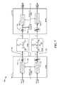
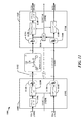
[0065]図5は、2つのデバイス502と532の間で提供されるマルチレーンインターフェース500の一例を示す図である。送信機502において、トランスコーダ506、516が、たとえばN階乗(N!)符号化を使用して、各レーン512、522上のN本のワイヤのセットを通じて送信されるべきシンボルにデータ504、514とクロック情報とを符号化するために使用され得る。クロック情報は、それぞれの送信クロック524、526から導出され、連続するシンボルの間のNC2個の信号のうちの少なくとも1つでシグナリング状態遷移が発生することを確実にすることによって、N本のワイヤを通じてNC2個の差動信号において送信されるシンボルのシーケンスの中で符号化され得る。N!符号化がN本のワイヤを駆動するために使用されるとき、シンボルの各ビットは、線ドライバ510、520のセットのうちの1つによって差動信号として送信され、ここで線ドライバ510、520のセットの中の差動ドライバはN本のワイヤの異なるペアに結合される。ワイヤのペアと信号との利用可能な組合せの数はNC2として計算されることが可能であり、利用可能な組合せの数は、N本のワイヤを通じて送信されることが可能な信号の数を決定する。シンボルにおいて符号化されることが可能なデータビット504、514の数は、各シンボル送信間隔に対して利用可能な、利用可能シグナリング状態の数に基づいて計算され得る。
FIG. 5 is a diagram illustrating an example of a
[0066]終端インピーダンス(通常は抵抗性)が、N本のワイヤの各々を終端ネットワーク528、530の中の共通中点に結合する。N本のワイヤのシグナリング状態は、各ワイヤに結合された差動ドライバ510、520に起因する終端ネットワーク528、530の中の電流の組合せを反映することが、理解されるだろう。終端ネットワーク528、530の中点はヌルポイントであり、これにより終端ネットワーク528、530の中の電流が中点において互いに打ち消すことがさらに理解されるだろう。
[0066] A termination impedance (usually resistive) couples each of the N wires to a common midpoint in termination network 528,530. It will be appreciated that the signaling state of the N wires reflects the combination of currents in the
[0067]リンクの中のNC2個の信号のうちの少なくとも1つが連続するシンボルとシンボルの間で遷移するので、N!符号化方式は、別個のクロックチャネルおよび/または0に戻らない復号を使用する必要がない。実質的に、各トランスコーダ506、516は、各シンボルが直前のシンボルとは異なるようなシンボルのシーケンスを産生することによって、N本のワイヤで送信されるシンボルの各ペアの間で遷移が発生することを確実にする。図5に示される例では、各レーン512、522はN=4本のワイヤを有し、4本のワイヤの各セットは4C2=6個の差動信号を搬送することができる。トランスコーダ506、516は、レーン512、522上で利用可能なN本のワイヤ上での送信のための生のシンボルを生成するために、あるマッピング方式を利用し得る。トランスコーダ506、516およびシリアライザ508、518は、入力データビット504、514に基づいて、送信のための生のシンボルを協力して産生する。受信機532において、トランスコーダ540、550は、たとえば、連続する生のシンボルのペアとルックアップテーブルの中のシンボルとの差を特徴付ける遷移数を決定するために、マッピングを利用し得る。トランスコーダ506、516、540、550は、生のシンボルの一つ一つの連続するペアが2つの異なるシンボルを含むということを基礎にして動作する。
[0067] Since at least one of the N C 2 signals in the link transitions between consecutive symbols, N! The encoding scheme does not need to use a separate clock channel and / or decoding that does not return to zero. In effect, each
[0068]送信機502におけるトランスコーダ506、516は、一つ一つのシンボル遷移において利用可能なN!−1個の状態の中から選択し得る。一例では、4!システムは、各シンボル遷移において送信されるべき次のシンボルのために4!−1=23個のシグナリング状態を提供する。ビットレートは、送信クロック524、526のサイクル当たりlog2(利用可能な状態)として計算され得る。ダブルデータレート(DDR)クロッキングを使用するシステムでは、シンボル遷移は、送信クロック524、526の立上りエッジと立下りエッジの両方で発生する。一例では、2つ以上のシンボルがワードごとに(すなわち、送信クロックサイクルごとに)送信されることが可能であるので、送信クロックサイクルにおける全体の利用可能な状態は(NC2−1)2=(23)2=529個であり、シンボル当たりの送信され得るデータビット504の数は、log2(529)=9.047ビットとして計算され得る。
[0068]
[0069]受信機デバイス532は、線受信機534、544のセットを使用してシンボルのシーケンスを受信し、ここで線受信機534、544のセットの中の各受信機は、N本のワイヤの1つのペアでのシグナリング状態の差を決定する。したがって、NC2個の受信機が各レーン512、522において使用され、ここでNは対応するレーン512、522におけるワイヤの数を表す。NC2個の受信機534、544は、対応する数の生のシンボルを出力として産生する。
[0069] The
[0070]図示される例では、各レーン512、522はN=4本のワイヤを有し、各レーン512、522の4本のワイヤで受信される信号は、対応するCDR536、546およびデシリアライザ538、548に提供される状態遷移信号を産生するために、6個の受信機(4C2=6)を含む線受信機534または544の対応するセットによって処理される。CDR536および546は、全般に図3のCDR300と同じ方式で動作することができ、各CDR536および546は、対応するデシリアライザ538、548によって使用されることが可能な受信クロック信号554、556を産生し得る。クロック信号554は、トランスコーダ540、550によって提供されるデータを受信するために外部回路によって使用されることが可能なDDRクロック信号を含み得る。各トランスコーダ540、550は、各々の次のシンボルをその直前と比較することによって、対応するデシリアライザ538、548から受信シンボルのブロックを復号する。トランスコーダ540、550は、送信機502に提供されるデータ504、514に対応する出力データ542と552とを産生する。
[0070] In the illustrated example, each
[0071]図5の例に示されるように、各レーン512、522は独立に動作し得るが、典型的な応用では、一方のレーン512を通じて送信されるデータ504は他方のレーン522を通じて送信されるデータ514と同期され得る。一例では、第1のレーン(この例ではレーンX)512を通じた送信のためのデータビット504は、所定のシーケンスで送信されると、第1のレーン512の4本のワイヤで送信される少なくとも1つの信号においてシグナリング状態の遷移が発生することを確実にする、生のシンボルのセットを生成する第1のトランスコーダ506によって受信される。シリアライザ508は、各シンボル間隔のための第1のレーン512の4本のワイヤのシグナリング状態を決定する線ドライバ510に提供されるシンボル値のシーケンスを産生する。同時に、データビット514が、第2のレーン(この例ではレーンY)522の第2のトランスコーダ516によって受信される。第2のトランスコーダ516は、各シンボル間隔のための第2のレーン522の4本のワイヤのシグナリング状態を決定する線ドライバ520に提供されるシンボル値のシーケンスへ遷移数のセットを変換するシリアライザ518によってシリアライズされる、遷移数のセットを生成する。生のシンボルのシーケンスは、連続するシンボルの各ペア間の第2のレーン522の4本のワイヤで送信される少なくとも1つの信号においてシグナリング状態の遷移が発生することを確実にする。
[0071] As shown in the example of FIG. 5, each
[0072]図6は、本明細書で開示されるいくつかの態様に従って提供されるマルチレーンインターフェース600の第1の例を示す。マルチレーンインターフェース600は、第1のレーン(ここではレーンX)612上で送信されるシンボルに符号化されたクロック情報が、レーンY622を含む1つまたは複数の他のレーン上の符号化されたクロック情報を伴わずに送信されたシンボルを受信するために使用されるとき、データスループットの改善と回路の複雑さの低減とをもたらす。図示される例では、各レーン612、622は4本のワイヤを含む。
[0072] FIG. 6 illustrates a first example of a
[0073]送信のためのデータは2つの部分604および614に分割されることがあり、ここで各部分は異なるレーン612、622上で送信される。第1のレーン612上で、データ604および送信クロック624に関する情報が、図5に関して説明されたようにシリアライズされる生のシンボルを取得するために、トランスコーダ/シリアライザ608を使用して符号化され得る。受信機632において、第1のレーン612と関連付けられる受信機634の出力はCDR636に提供される。CDR636は、両方のレーン612、622のためのデシリアライズおよびトランスコード回路638と648の両方によって使用される受信クロック654を生成するために、シグナリング状態の遷移を検出するように構成され得る。第1のデシリアライズ回路およびトランスコード回路638は、第1のレーン612から受信された生のシンボルからデータ642を抽出し、一方で、第2のデシリアライズ回路およびトランスコード回路648は、第2のレーン622から受信された生のシンボルからデータ652を抽出する。
[0073] Data for transmission may be divided into two
[0074]第2のレーン622のために、送信データ614が、トランスコード回路およびシリアライズ回路618に提供され、符号化されたクロック情報を伴わずに第2のレーン622上で送信され得る。第2のレーン622のための生のシンボルを産生するために使用されるトランスコード回路は、第1のレーン612上での送信のために埋め込まれたクロック情報とともに生のシンボルを産生するために使用されるトランスコード回路よりも、はるかに複雑ではないことがある。たとえば、第2のレーン622のためのトランスコード回路は、一つ一つのシンボル境界における状態遷移を保証するために、いくつかの算術演算と論理関数とを実行する必要がないことがある。
[0074] For the
[0075]図6に示される例では、DDRクロッキングされた4ワイヤの第1のレーン612は、(4!−1)2=(23)2=529個のシグナリング状態を提供し、受信されたワード604、614当たりlog2529=9.047ビットのデータを符号化することができ、一方でDDRクロッキングされた4ワイヤの第2のレーン622は、(4!)2=(24)2=576個のシグナリング状態を提供し、ワード当たりlog2576=9.170ビットのデータを符号化することができる。別の例では、インターフェースは2つの3ワイヤレーンを有することがあり、ここでクロック情報は第1のレーンにおいては符号化されるが、第2のレーンでは符号化されない。この後者の例では、ワード当たり7個のシンボルが送信されることがあり、3ワイヤの第1のレーンは、(3!−1)7=(5)7=78125個のシグナリング状態を提供し、ワード当たりlog278125=16.253ビットのデータを符号化することができ、一方で3ワイヤの第2のレーンは、(3!)7=(6)7=279936個のシグナリング状態を提供し、各クロックサイクルにおいてlog2279936=18.095ビットのデータを符号化することができる。マルチレーンN!の単一のレーンにおいてクロック情報を符号化することによって、より高い全体のスループットが、より少ないハードウェアで実現され得る。
[0075] In the example shown in FIG. 6, DDR clocked 4-wire
[0076]図7は、本明細書で開示される1つまたは複数の態様に従って提供されるマルチレーンインターフェース700の別の例を示す。マルチレーンインターフェース700は、データスループットの最適化および回路の複雑さの低減に加えて、設計の柔軟性の改善をもたらす。ここでは、1つのレーン(ここではレーンX)712で送信されるシンボルに符号化されるクロック情報が、異なる数のワイヤを有する1つまたは複数の他のレーン722で送信されるシンボルを受信するために使用され得る。
[0076] FIG. 7 illustrates another example of a
[0077]図示される例では、送信のためのデータは複数の部分704および714に分割されることがあり、ここで各部分は異なるレーン712、722で送信されることになる。第1のレーン712上で、データ704および送信クロック724は、図5および図6に関して説明されたように生のシンボルのシーケンスを取得するために、トランスコード回路およびシリアライズ回路708によって変換され得る。第2のレーン722上で、受信されたデータ714が、トランスコード回路およびシリアライズ回路718に提供され、次いで、埋め込まれたクロック情報を伴わずに送信され得る。
[0077] In the illustrated example, the data for transmission may be divided into
[0078]受信機732において、第1のレーン712と関連付けられる受信機734の出力はCDR736に提供される。CDR736は、第1のレーン712の中の3本のワイヤのシグナリング状態の遷移を検出し、両方のレーン712、722のためのデシリアライズ回路およびトランスコード回路738と748の両方によって使用される受信クロック754を生成するように構成され得る。第1のデシリアライズ回路およびトランスコード回路738は、第1のレーン712から受信された生のシンボルからデータ742を抽出し、一方で、第2のデシリアライズ回路およびトランスコード回路748は、第2のレーン722から受信された生のシンボルからデータ752を抽出する。
[0078] At the
[0079]例では、第1のレーン712は3!動作のために構成された3本のワイヤを含むが、第2のレーン722は4!動作のために構成された4本のワイヤを含む。第1のレーン712は、ワード当たり2シンボルのシステムに対して(3!−1)2=(5)2=25個のシグナリング状態を提供することができ、これにより、log225=4.644ビットのデータがワードごとに符号化され得る。4ワイヤの第2のレーン722は、(4!)2=(24)2=576個のシグナリング状態を提供し、ワードごとにlog2576=9.170ビットのデータを符号化することができる。
[0079] In the example, the
[0080]単一のレーン712がクロック情報を符号化し、可変の数のワイヤが他のレーン722に割り当てられ得るときに、大きな効率が得られ得る。10個の相互接続(ワイヤまたはコネクタ)が2つのデバイスの間で利用可能である例では、従来の3!システムは3つの3ワイヤレーンを構成することがあり、このとき各レーン上にクロック情報が符号化される。3つのレーンの各々が、全体でシンボル当たり15個の状態に対して、シンボル当たり5個のシグナリング状態を提供する。しかしながら、本明細書で説明されるいくつかの態様に従って提供されるシステムは、2つの3!レーンと1つの4!レーンとを提供するために10個の相互接続を使用することができ、ここでクロック情報は第1の3!レーンにおいて符号化される。レーンのこの組合せは、シンボル当たり5個の状態とクロック情報とを提供する第1の3!レーン、シンボル当たり6個の状態を提供する第2の3!レーン、およびシンボル当たり24個の状態を提供する4!レーンに基づいて、全体でシンボル当たり5×6×24=720個のシグナリング状態を提供する。
[0080] Great efficiency can be obtained when a
[0081]図8は、本明細書で開示される1つまたは複数の態様に従って提供されるマルチレーンインターフェース800の別の例を示す。マルチレーンインターフェース800は、改善された復号の信頼性を含む様々な利点をもたらし、これはより高い送信レートを可能にし得る。この例でのマルチレーンインターフェース800の構成および動作は、CDR836が第1のレーン812または第2のレーン822のいずれかで検出される遷移から受信クロック854を生成するように構成されることを除き、図6のマルチレーンインターフェース600の構成および動作と同様である。したがって、CDR836は受信機834および844の出力を受信する。CDR836はレーン812または822のいずれかでの最初に検出された遷移からクロックを生成するので、シンボル境界と受信クロック854のエッジとの間の遅延の変動が低減され得る。この手法は、線ドライバ810、820または受信機834、844の、ワイヤ上の可変の遷移時間および/または可変のスイッチング時間の影響を減らすことができる。
[0081] FIG. 8 illustrates another example of a
[0082]動作において、送信のためのデータは2つ以上の部分804および814において受信されることがあり、ここで部分804、814は、異なるレーン812、822上での送信のためのものである。図5に関して説明されるように、トランスコーダ回路とシリアライザ回路808の組合せは、データビットX804を符号化し、第1のレーン812で送信されるべきシンボルのシーケンスに、送信クロック824に関する情報を埋め込むことができる。受信機832において、受信機834および844の両方のセットの出力がCDR836に与えられ、CDR836は、レーン812、822のいずれかでのシグナリング状態の遷移を検出し、遷移に基づいて受信クロック854を生成するように構成される。受信クロック854は、デシリアライズ/トランスコード回路838と848の両方によって使用され、デシリアライズ/トランスコード回路838および848はそれぞれの第1のレーンデータ出力842および第2のレーンデータ出力852を産生する。
[0082] In operation, data for transmission may be received in two or
[0083]図9は、本明細書で開示される1つまたは複数の態様に従って提供されるマルチレーンインターフェース900の別の例を示す。この例では、マルチレーンインターフェース900は、連続的なシンボル間隔とシンボル間隔の間のシグナリング状態の遷移が複数のレーン912、922のいずれか1つで発生することを確実にすることによって、改善されたデータスループットと符号化の効率性とを提供する。したがって、クロック情報を符号化することと関連付けられるパーセンテージオーバーヘッドは、単一のレーンで送信されるシンボルのシーケンスにクロック情報が埋め込まれるシステムより相対的に低減され得る。マルチレーンインターフェース900では、第1のレーン(ここではレーンX)912は、3!個の符号化された信号を搬送する3本のワイヤを含み、一方で第2のレーン(ここではレーンY)922は4本のワイヤを含み、4!符号化のために構成される。異なる数および構成のレーンが利用されることがあり、図9に図示される具体的な例は例示のみを目的に与えられる。トランスコーダ906は、2つ以上のレーン912および/または922を通じて送信されるべきシンボルにおいてデータ904とクロック情報とを合成するように適合され得る。
[0083] FIG. 9 illustrates another example of a
[0084]すべてのレーン912、922に対する利用可能なシグナリング状態の組合せに基づいてクロック情報を埋め込むことによって、符号化の効率性が実現され得る。連続するシンボル間隔とシンボル間隔との間に少なくとも1つのレーン912、922でシグナリング状態の遷移が発生することを確実にすることによって、クロック情報が埋め込まれる。動作において、トランスコーダ906は、各レーン912、922のためにシンボルの異なるセットを産生するように構成され得る。一例では、クロック信号924に従って送信機902によって受信されるデータ904は、3!の第1のレーン912で送信される3つの信号に符号化されるシンボルの第1のシーケンスおよび4!の第2のレーン922で同時に送信される6つの信号に符号化されるシンボルの第2のシーケンスとして送信され得る。トランスコーダ906は、連続するシンボルとシンボルの間にレーン912と922の少なくとも1つでシグナリング状態遷移が発生することを確実にすることによって、クロック情報を埋め込む。シンボル間隔当たりの状態の総数は、第1のレーン912で送信されるシンボル当たりの状態の数と第2のレーン922で送信されるシンボル当たりの状態の数との積である。したがって、各シンボル間隔においてトランスコーダに対して利用可能な状態の数は、クロック情報が両方のレーン912、922にわたって埋め込まれるとき、次のように計算され得る。
(Nlane1!×Nlane2!)−1=(3!×4!)−1=(6×24)−1=143
別の例では、各シンボル間隔においてトランスコーダに対して利用可能な状態の数は、クロック情報が3!を使用する3つの信号に符号化される2つのレーンにわたって埋め込まれるとき、次のように計算され得る。
(NlaneX!×NlaneY!)−1=(3!×3!)−1=(6×6)−1=35
[0084] Encoding efficiency may be achieved by embedding clock information based on a combination of available signaling states for all
(N lane1 ! × N lane2 !)-1 = (3! × 4!)-1 = (6 × 24) -1 = 143
In another example, the number of states available to the transcoder in each symbol interval is 3! Can be computed as follows when embedded over two lanes encoded into three signals using:
(N laneX ! × N laneY !) − 1 = (3! × 3!) − 1 = (6 × 6) −1 = 35
[0085]各シンボル遷移においてトランスコーダに対して利用可能な状態の数は、各受信データサイクルにおいて送信され得るビットの数を支配する。 [0085] The number of states available to the transcoder at each symbol transition governs the number of bits that can be transmitted in each received data cycle.

[0086]表1および表2は、クロック情報が2つ以上のN!レーンにわたってトランスコーダによって埋め込まれるときの、コーディング効率の向上を示す。表1は図9のマルチレーンインターフェース900に関係する。表から理解され得るように、トランスコーダ906が両方のレーン912、922で送信されるシンボルのシーケンスを考慮することによってクロック情報を埋め込むときに、最大の符号化効率が得られる。
[0086] Tables 1 and 2 show that N! Fig. 5 shows the coding efficiency improvement when embedded by a transcoder across lanes. Table 1 relates to the
表2は2つの3!レーンを有するマルチレーンインターフェースの例に関係する。 Table 2 shows two 3! This relates to an example of a multi-lane interface with lanes.
[0087]図9の例では、受信機932は、両方のレーン912、922での遷移を検出することによって受信クロック954を生成するCDR936を含む。デシリアライザ938、948は、送信機の中のトランスコーダ906によって実行されるトランスコーディングを反転させるトランスコーダ940に、それぞれのレーン912、922から受信されたシンボルを提供する。受信機932の中のトランスコーダ940は、出力データ942を産生するために受信されたシンボルの合成されたシーケンスを検査することによって動作し、出力データ942は送信機902において受信されるデータ904に対応する。線ドライバ910、920および受信機934、944のセットは、N!レーン912、922の中のワイヤの数に従って提供され得る。
[0087] In the example of FIG. 9, the
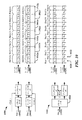
[0088]マルチレーンインターフェース900は、従来のインターフェースを上回る追加の利点を提供するように構成され得る。図10は、受信機へのデータの配信の順序を制御するためにトランスコーダ1024が使用され得る例を示す。図5のマルチレーンインターフェース500などの1つのマルチレーンインターフェース1000が、対応する数のレーンを通じた送信のために、シンボル1006、1008のシーケンスにデータビット1002、1004の2つ以上のセットを独立に符号化し得る。データはデータビット1002、1004のセットへと事前に分けられたマルチレーンインターフェース1000に提供されることがあり、および/または、データビット1002、1004のセットはマルチレーンインターフェース1000によって分割されることがある。データビットは、機能、設計選好に従って、または利便性および/もしくは他の理由で、データビット1002、1004の2つ以上のセットの間で任意に割り振られ得る。
[0088] The
[0089]示されるマルチレーンインターフェース1000では、第1のクロックサイクルにおいて受信される各ワード、バイト、または他のデータ要素は、2つのレーンのうちの1つでシンボル間隔1012a〜1012gのペアにおいて順番に送信される2つ以上のシンボルへと符号化され得る。受信機は、2つ以上のシンボルがシンボル間隔1012a〜1012gのペアから受信されるとき、データ要素を復号することができる。
[0089] In the illustrated
[0090]図9のマルチレーンインターフェース900などのマルチレーンインターフェース1020は、2つ以上のレーンを通じて同時に送信されるシンボルの複数のシーケンス1026、1028へとデータ1022とクロック情報とを符号化する、トランスコーダ1024を含み得る。トランスコーダ1024は、2つのレーンでの送信のためにシンボルを同時に送信することによって、受信機へのデータの配信の順序を制御し得る。一例では、第1のクロックサイクルにおいて受信されるデータビット1022(Bits(0))は、2つのシンボルへとトランスコードされ、第1のシンボル間隔1030の間に2つのレーンで並列に送信され得る。第2のクロックサイクルにおいて受信されるデータビット1022(Bits(1))は、第2のシンボル間隔1032の間に2つのレーンで並列に2つのシンボルとして送信され得る。2つの並列なデータレーンでのデータの送信は、カメラのシャッターおよび/またはフラッシュ制御、ゲームアプリケーションと関連付けられる制御信号などの、タイミングに敏感な用途で一定の利益をもたらし得る。
[0090] A
[0091]図11は、本明細書で開示される1つまたは複数の態様に従って提供されるマルチレーンインターフェース1100の別の例を示す。この例では、マルチレーンインターフェース1100は、少なくとも1つのN!符号化されるレーン1112とシリアルデータリンク1122とを含む。シリアルデータリンク1122は、シングルエンドのシリアルリンク(図示されるような)または差動的に符号化されるシリアルデータリンクであり得る。シリアルデータリンク1122は、集積回路間(I2C)バス、カメラ制御インターフェース(CCI)シリアルバス、またはこれらのシリアルバス技術の派生物などの、シリアルバスを含み得る。図示される例では、クロック信号1124が、N!リンクのシリアライザ1108およびシリアルリンク1122のシリアライザ1118によって使用され、クロック信号1124は、別個のクロック信号レーンを通じて受信機1132に送信される必要がない。代わりに、トランスコーダ1106が、N!レーン1112の差動線ドライバにシリアライザを通じて提供されるシンボルのシーケンスにクロック情報を埋め込む。
[0091] FIG. 11 illustrates another example of a
[0092]受信機1132において、CDR1136が、受信機1134の出力において検出される遷移から受信機クロック信号1154を生成する。受信機クロック信号1154は、N!レーンデシリアライザ1138およびシリアルリンクデシリアライザ1148によって使用される。いくつかの事例では、CDR1136は、シンボル間隔とシンボル間隔の間での遷移の検出を改善するために、シリアルリンク1122と関連付けられる線受信機1144の出力を監視し得る。N!レーンデシリアライザ1138は、デシリアライズされたシンボル情報をトランスコーダ1140に提供し、トランスコーダ1140は、N!符号化されるレーン1112を通じて送信される入力データ1104を表す出力データ1142を産生する。
[0092] At the
[0093]一例では、送信機1102は、3!符号化される第1のレーン1112で3つの信号においてシンボルを送信する。シンボルは埋め込まれたクロック情報を含み、シンボル当たり5個のシグナリング状態が第1のレーン1112で利用可能である。送信機はまた、シリアルリンク1122のワイヤで送信される4つのシリアル信号を使用して、第2のレーンでデータを送信し得る。受信機1132は、第1のレーン1112で送信されるシンボルからクロック信号1154を生成することができ、ここでクロックは、両方のレーン1112、1122で送信されるデータを復号/デシリアライズするために使用される。したがって、シリアルリンク1122は、CDR1136によって提供されるクロック1154が第2のレーンシリアルリンク1122のためのデシリアライザ1148によって使用されるとき、シンボル当たり24=16個の状態を提供する。CDR1136によって提供されるクロック1154が使用されるとき、総計でシンボル当たり5×16=80個の状態が達成される。
[0093] In one example,
[0094]比較として、従来の、または通常の4ワイヤのシリアルリンク1122は、4本のワイヤのうちの1本を、クロック信号の搬送専用にすることがあり、データ送信は4本のワイヤのうちの他の3本の3つの信号に限定されることがある。この後者の構成では、シンボル当たり23=8個のシグナリング状態がシリアルリンク1122上で提供されることが可能であり、データが3!符号化された第1のレーン1112においても送信されるとき、総計でシンボル当たり5×8=40個のシグナリング状態が得られる。
[0094] As a comparison, a conventional or regular 4-wire
[0095]図12は、Nワイヤ通信リンク上でのデータ通信のための方法を示すフローチャート1200である。通信リンクは、N!符号化、マルチフェーズ符号化、マルチワイヤ差動符号化などの適切な符号化方式を使用して符号化されるシンボルを搬送する、複数のコネクタを含み得る。コネクタは、導電性ワイヤ、光信号導体、半導体相互接続などを含み得る。方法は、受信デバイスの1つまたは複数のプロセッサによって実行され得る。
[0095] FIG. 12 is a
[0096]ステップ1202において、シンボルの第1のシーケンスが、マルチレーンインターフェースの第1のレーンから受信される。シンボルのシーケンスの中の各シンボルは、第1のレーンのN本のワイヤのシグナリング状態に対応し得る。
[0096] In
[0097]ステップ1204において、クロック信号がマルチレーンインターフェースから復元または抽出される。クロック信号は、シンボルの第1のシーケンスの中の連続するシンボルのペアとペアの間に、N本のワイヤのシグナリング状態の複数の遷移に対応するエッジを含み得る。
[0097] In
[0098]ステップ1206において、シンボルの第1のシーケンスが、クロック信号を使用してデータビットの第1のセットに変換される。シンボルの第1のシーケンスは、シンボルの第1のシーケンスを遷移数のセットに変換するためにトランスコーダを使用すること、およびデータビットの第1のセットを得るために遷移数のセットを変換することによって、データビットの第1のセットに変換され得る。
[0098] In
[0099]ステップ1208において、データビットの第2のセットが、クロック信号を使用してマルチレーンインターフェースの第2のレーンから受信される1つまたは複数の信号から導出される。データビットの第2のセットは、トランスコーダを使用せずに導出され得る。
[0099] In
[00100]本明細書で開示されるいくつかの態様によれば、シンボルの第1のシーケンスは、N本のワイヤのNC2個の異なるペアから受信されるNC2個の差動信号に符号化され得る。第2のレーンはM本のワイヤを含むことがあり、ここで、シンボルの第2のシーケンスは、M本のワイヤのMC2個の異なるペアから受信されるMC2個の差動信号に符号化される。MおよびNは、等しい値または異なる値を有し得る。 According to some embodiments [00100] disclosed herein, a first sequence of symbols, N C 2 pieces of differential signals received from the N C 2 pieces of different pairs of the N wires Can be encoded. The second lane may contain M of wires, wherein the second sequence of symbols, M C 2 pieces of differential signals received from M C 2 pieces of different pairs M of wires Is encoded. M and N can have equal or different values.
[00101]本明細書で開示されるいくつかの態様によれば、データビットの第2のセットを導出することは、シリアルインターフェースのM本のワイヤの各々からシリアル信号を受信することと、クロック信号に従ってシリアル信号をサンプリングすることによってデータビットの第2のセットを抽出することとを含む。データビットの第2のセットを導出することは、シリアルインターフェースのM本のワイヤからM/2個の差動信号を受信することと、クロック信号に従ってM/2個の差動信号をサンプリングすることによってデータビットの第2のセットを抽出することとを含む。 [00101] According to some aspects disclosed herein, deriving the second set of data bits includes receiving a serial signal from each of the M wires of the serial interface, and a clock. Extracting a second set of data bits by sampling the serial signal according to the signal. Deriving the second set of data bits includes receiving M / 2 differential signals from the M wires of the serial interface and sampling the M / 2 differential signals according to the clock signal. Extracting a second set of data bits.
[00102]本明細書で開示されるいくつかの態様によれば、クロック信号は、N本のワイヤのシグナリング状態または第2のレーンの1つまたは複数のワイヤのシグナリング状態において検出される遷移に対応する、クロック信号の遷移を提供することによって、復元または抽出され得る。クロック信号は、マルチレーンインターフェースの第2のレーンの少なくとも1本のワイヤのシグナリング状態の1つまたは複数の遷移に対応するエッジを含み得る。 [00102] According to some aspects disclosed herein, a clock signal is transmitted to a transition detected in the signaling state of the N wires or the signaling state of one or more wires in the second lane. By providing corresponding clock signal transitions, they can be recovered or extracted. The clock signal may include an edge corresponding to one or more transitions in the signaling state of at least one wire of the second lane of the multilane interface.
[00103]本明細書で開示されるいくつかの態様によれば、シンボルの第1のシーケンスはNC2個の差動信号に符号化される。NC2個の差動信号の各々が、N本のワイヤの異なるペアから受信され得る。シンボルの第2のシーケンスは、第2のレーンのM本のワイヤから受信されるMC2個の差動信号に符号化され得る。MC2個の差動信号の各々が、M本のワイヤの異なるペアから受信され得る。シンボルの第1のシーケンスは、トランスコーダ回路を使用してデータビットの第1のセットに変換され得る。シンボルの第2のシーケンスは、同じトランスコーダ回路を使用してデータビットの第2のセットに変換され得る。 [00103] According to some aspects disclosed herein, the first sequence of symbols is encoded into N C 2 differential signals. Each of the N C 2 differential signals may be received from a different pair of N wires. The second sequence of symbols may be encoded into M C 2 differential signals received from the M wires of the second lane. Each of the M C 2 differential signals may be received from a different pair of M wires. The first sequence of symbols may be converted to a first set of data bits using a transcoder circuit. The second sequence of symbols can be converted to a second set of data bits using the same transcoder circuit.
[00104]本明細書で開示されるいくつかの態様によれば、N本のワイヤおよびM本のワイヤのうちの1つまたは複数のシグナリング状態の遷移は、シンボルの第1のシーケンスの中のシンボルの各々の順次的なペアとペアの間で発生する。シンボルの第1のシーケンスの各々は、異なるシンボル間隔において送信され得る。各シンボル間隔において受信されるデータビットの第1のセットおよびデータビットの第2のセットは、各シンボル間隔からの完全なデータ要素を得るために組み合わされ得る。 [00104] According to some aspects disclosed herein, a transition of one or more signaling states of the N wires and the M wires is performed in a first sequence of symbols. Occurs between each sequential pair of symbols. Each of the first sequence of symbols may be transmitted in a different symbol interval. The first set of data bits and the second set of data bits received in each symbol interval may be combined to obtain a complete data element from each symbol interval.
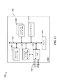
[00105]図13は、処理回路1302を利用する装置1300のためのハードウェア実装形態の簡略化された例を示す図である。処理回路は、一般に、マイクロプロセッサ、マイクロコントローラ、デジタル信号プロセッサ、シーケンサおよび状態機械のうちの1つまたは複数を含み得るプロセッサ1316を有する。処理回路1302は、バス1320によって全般に表されるバスアーキテクチャを用いて実装され得る。バス1320は、処理回路1302の具体的な適用例および全体的な設計制約に応じて、任意の数の相互接続バスおよびブリッジを含み得る。バス1320は、プロセッサ1316、モジュールならびに/または回路1304、1306、および1308、コネクタまたはワイヤ(マルチレーンインターフェース)1314を通じて通信するように構成可能な線インターフェース回路1312、ならびにプロセッサ可読/コンピュータ可読記憶媒体1318によって表される、1つまたは複数のプロセッサおよび/またはハードウェアモジュールを含む様々な回路を一緒につなぐ。バス1320はまた、タイミングソース、周辺機器、電圧調節器、および電力管理回路などの、様々な他の回路をつなぎ得るが、これらの回路は当技術分野においてよく知られており、したがって、これ以上説明されない。
[00105] FIG. 13 is a diagram illustrating a simplified example of a hardware implementation for an
[00106]プロセッサ1316は、コンピュータ可読記憶媒体1318に記憶されたソフトウェアの実行を含む一般的な処理を担当する。ソフトウェアは、プロセッサ1316によって実行されると、処理回路1302に、任意の特定の装置のための上で説明された様々な機能を実行させる。コンピュータ可読記憶媒体1318はまた、コネクタ1314を通じて送信されるシンボルから復号されるデータを含む、ソフトウェアを実行するときにプロセッサ1316によって操作されるデータを記憶するために使用され得る。処理回路1302はさらに、モジュールならびに/または回路1304、1306、および1308のうちの少なくとも1つを含む。モジュールならびに/または回路1304、1306および1308は、コンピュータ可読記憶媒体1318に存在する/記憶された、プロセッサ1316において動作するソフトウェアモジュールであるか、プロセッサ1316に結合された1つまたは複数のハードウェアモジュールであるか、またはそれらの何らかの組合せであり得る。モジュールならびに/または回路1304、1306および/もしくは1308は、マイクロコントローラ命令、状態機械構成パラメータ、またはそれらの何らかの組合せを含み得る。
[00106] The
[00107]一構成では、ワイヤレス通信のための装置1300は、マルチレーンインターフェース1314の第1のレーンからシンボルの第1のシーケンスを受信するように構成されるモジュールおよび/または回路1306、1312と、マルチレーンインターフェース1314からクロック信号を復元するように構成されるモジュールおよび/または回路1306と、ここにおいて、クロック信号が、シンボルの第1のシーケンスの中の連続するシンボルのペアとペアの間でN本のワイヤのシグナリング状態の複数の遷移に対応するエッジが発生するを含む、クロック信号を使用してシンボルの第1のシーケンスをデータビットの第1のセットに変換するように構成されるモジュールならびに/または回路1304および/もしくは1308と、クロック信号を使用してマルチレーンインターフェース1314の第2のレーンから受信される1つまたは複数の信号からデータビットの第2のセットを導出するように構成されるモジュールならびに/または回路1304および/もしくは1308とを含む。一例では、図6〜図9および図11に示される回路は、処理回路1302によって実行される様々な機能を実装する論理を提供する。
[00107] In one configuration, an
[00108]本開示のある態様では、コンピュータ可読記憶媒体1318は、1つまたは複数の命令を記憶または維持している。処理回路1302の少なくとも1つのプロセッサ1316によって実行されると、命令は、処理回路1302に、マルチレーンインターフェース1314の第1のレーンからシンボルの第1のシーケンスを受信させ、マルチレーンインターフェース1314からクロック信号を復元させ、ここにおいて、クロック信号が、シンボルの第1のシーケンスの中の連続するシンボルのペアとペアの間のN本のワイヤのシグナリング状態の複数の遷移に対応するエッジを含む、クロック信号を使用してシンボルの第1のシーケンスをデータビットの第1のセットへ変換させ、クロック信号を使用してマルチレーンインターフェース1314の第2のレーンから受信される1つまたは複数の信号からデータビットの第2のセットを導出させ得る。シンボルのシーケンスの中の各シンボルは、N本のワイヤのシグナリング状態に対応し得る。
[00108] In certain aspects of the present disclosure, the computer-
[00109]前述の手段は、たとえば、プロセッサ206または236の何らかの組合せ、物理層ドライバ210または240、および記憶媒体208および238を使用して実装され得る。
[00109] The foregoing means may be implemented using, for example, some combination of
[00110]図14は、Nワイヤ通信リンク上でのデータ通信のための方法を示すフローチャート1400である。通信リンクは、N!符号化、マルチフェーズ符号化、マルチワイヤ差動符号化などの適切な符号化方式を使用して符号化されるシンボルを搬送する、複数のコネクタを含み得る。コネクタは、導電性ワイヤ、光信号導体、半導体相互接続などを含み得る。方法は、受信デバイスの1つまたは複数のプロセッサによって実行され得る。
[00110] FIG. 14 is a
[00111]ステップ1402において、クロック情報が、第1のデータビットを符号化するシンボルの第1のシーケンスに埋め込まれる。シンボルの第1のシーケンスの各々は、マルチレーンインターフェースの第1のレーンのN本のワイヤのシグナリング状態に対応し得る。クロック情報は、第1のデータビットを遷移数のセットに変換するためにトランスコーダを使用することによって符号化されることがあり、シンボルの第1のシーケンスを取得するために遷移数のセットを変換することができる。第2のデータビットは、トランスコーダを使用することなくシンボルの第2のシーケンスに符号化され得る。
[00111] At
[00112]ステップ1404において、シンボルの第1のシーケンスが第1のレーンで送信される。
[00112] In
[00113]ステップ1406において、シンボルの第2のシーケンスが、マルチレーンインターフェースの第2のレーンで送信される。シンボルの第2のシーケンスは、第2のデータビットとともに、また埋め込まれたクロック情報を伴わずに符号化され得る。
[00113] At
[00114]本明細書で開示されるいくつかの態様によれば、シンボルの第1のシーケンスは、N本のワイヤのNC2個の異なるペア上のNC2個の差動信号においてシンボルの第1のシーケンスを送信することによって送信され得る。第2のレーンはM本のワイヤを含み得る。シンボルの第2のシーケンスは、M本のワイヤのMC2個の異なるペア上のMC2個の差動信号において送信され得る。MおよびNの値は、等しくても異なっていてもよい。 According to some aspects disclosed [00114] herein, first the sequence, N of wires of N C 2 pieces of different symbols in the N C 2 pieces of differential signals on a pair of symbols May be transmitted by transmitting the first sequence of The second lane may include M wires. Second sequence of symbols may be sent in M C 2 pieces of differential signals on M C 2 pieces of different pairs of M of wires. The values of M and N may be equal or different.
[00115]本明細書で開示されるいくつかの態様によれば、シンボルの第2のシーケンスは、シリアルバスのM本のワイヤで送信され得る。シンボルの第2のシーケンスを送信することは、M/2の差動信号においてデータの第2のセットを送信することを含み得る。 [00115] According to some aspects disclosed herein, the second sequence of symbols may be transmitted on the M wires of the serial bus. Transmitting the second sequence of symbols may include transmitting a second set of data in M / 2 differential signals.
[00116]本明細書で開示されるいくつかの態様によれば、シンボルの第1のシーケンスの各々が異なるシンボル間隔において送信される。クロック情報を埋め込むことは、シンボルの第1のシーケンスの中の連続するシンボルの各ペア間での、N本のワイヤのシグナリング状態に、または第2のレーンの1つまたは複数のワイヤのシグナリング状態に、遷移を引き起こすことを含み得る。 [00116] According to some aspects disclosed herein, each of the first sequence of symbols is transmitted in a different symbol interval. Embedding clock information may be in the signaling state of N wires or the signaling state of one or more wires in the second lane between each pair of consecutive symbols in the first sequence of symbols. Can include causing a transition.
[00117]本明細書で開示されるいくつかの態様によれば、単一のトランスコーダ回路は、シンボルの第1のシーケンスに第1のデータビットを符号化するために、およびシンボルの第2のシーケンスに第2のデータビットを符号化するために使用され得る。 [00117] According to some aspects disclosed herein, a single transcoder circuit encodes a first data bit into a first sequence of symbols and a second of symbols. Can be used to encode the second data bit in the sequence.
[00118]本明細書で開示されるいくつかの態様によれば、クロック情報を埋め込むことは、シンボルの第1のシーケンスの中の連続するシンボルの各ペア間でのN本のワイヤのシグナリング状態に、または、シンボルの第2のシーケンスの中の連続するシンボルの各ペア間での第2のレーンのM本のワイヤのシグナリング状態に、遷移を引き起こすことを含む。クロック情報は、シンボルの第1のシーケンスとシンボルの第2のシーケンスの両方を符号化するために使用される送信クロックに関し得る。 [00118] In accordance with certain aspects disclosed herein, embedding clock information is the signaling state of N wires between each pair of consecutive symbols in the first sequence of symbols. Or causing a transition in the signaling state of the M wires in the second lane between each pair of consecutive symbols in the second sequence of symbols. The clock information may relate to a transmit clock that is used to encode both the first sequence of symbols and the second sequence of symbols.
[00119]本明細書で開示されるいくつかの態様によれば、データ要素は、データビットの第1のセットおよびデータビットの第2のセットを得るために分割され得る。データビットの第1のセットに対応する第1のシンボルは、第2のレーン上のデータビットの第2のセットに対応する第2のシンボルの送信と同時に、第1のレーンで送信され得る。 [00119] According to some aspects disclosed herein, the data elements may be partitioned to obtain a first set of data bits and a second set of data bits. The first symbol corresponding to the first set of data bits may be transmitted on the first lane simultaneously with the transmission of the second symbol corresponding to the second set of data bits on the second lane.
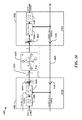
[00120]図15は、処理回路1502を利用する装置1500のためのハードウェア実装形態の簡略化された例を示す図である。処理回路は、一般に、マイクロプロセッサ、マイクロコントローラ、デジタル信号プロセッサ、シーケンサおよび状態機械のうちの1つまたは複数を含み得るプロセッサ1516を有する。処理回路1502は、バス1520によって全般に表されるバスアーキテクチャを用いて実装され得る。バス1520は、処理回路1502の具体的な適用例および全体的な設計制約に応じて、任意の数の相互接続バスおよびブリッジを含み得る。バス1520は、プロセッサ1516、モジュールおよび/または回路1504、1506、および1508、コネクタまたはワイヤ1514を通じて通信するように構成可能な線インターフェース回路1512、ならびにプロセッサ可読/コンピュータ可読記憶媒体1518によって代表される、1つまたは複数のプロセッサおよび/またはハードウェアモジュールを含む様々な回路を一緒につなぐ。バス1520はまた、タイミングソース、周辺機器、電圧調節器、および電力管理回路などの、様々な他の回路をつなぎ得るが、これらの回路は当技術分野においてよく知られており、したがって、これ以上説明されない。
[00120] FIG. 15 is a diagram illustrating a simplified example of a hardware implementation for an
[00121]プロセッサ1516は、コンピュータ可読記憶媒体1518に記憶されたソフトウェアの実行を含む一般的な処理を担当する。ソフトウェアは、プロセッサ1516によって実行されると、処理回路1502に、任意の特定の装置のための上で説明された様々な機能を実行させる。コンピュータ可読記憶媒体1518はまた、コネクタ1514を通じて送信されるシンボルから復号されるデータを含む、ソフトウェアを実行するときにプロセッサ1516によって操作されるデータを記憶するために使用され得る。処理回路1502はさらに、モジュールならびに/または回路1504、1506、および1508のうちの少なくとも1つを含む。モジュールならびに/または回路1504、1506および1508は、コンピュータ可読記憶媒体1518に存在する/記憶された、プロセッサ1516において動作するソフトウェアモジュールであるか、プロセッサ1516に結合された1つまたは複数のハードウェアモジュールであるか、またはそれらの何らかの組合せであり得る。モジュールならびに/または回路1504、1506および/もしくは1508は、マイクロコントローラ命令、状態機械構成パラメータ、またはそれらの何らかの組合せを含み得る。
[00121] The
[00122]一構成では、ワイヤレス通信のための装置1500は、シンボルの第1のシーケンスに符号化される第1のデータビットとともに情報を埋め込むように構成されるモジュールおよび/または回路1504と、マルチレーンインターフェース第1のレーンの第1のレーンでシンボルの第1のシーケンスを送信するように構成されるモジュールおよび/または回路1506、1512と、マルチレーンインターフェースの第2のレーンでシンボルの第2のシーケンスを送信するように構成されるモジュールならびに/または回路1504、1506、および/もしくは1508を含む。一例では、図6〜図9および図11に示される回路は、処理回路1502によって実行される様々な機能を実装する論理を提供する。
[00122] In one configuration, an
[00123]本開示のある態様では、プロセッサ可読/コンピュータ可読記憶媒体1518は、1つまたは複数の命令を記憶または維持している。処理回路1502の少なくとも1つのプロセッサ1516によって実行されると、命令は、プロセッサ1516に、シンボルの第1のシーケンスに符号化された第1のデータビットとともにクロック情報を埋め込ませ、マルチレーンインターフェース1514の第1のレーンでシンボルの第1のシーケンスを送信させ、マルチレーンインターフェース1514の第2のレーンでシンボルの第2のシーケンスを送信させ得る。シンボルの第1のシーケンスの各々は、マルチレーンインターフェース1514の第1のレーンのN本のワイヤのシグナリング状態に対応し得る。シンボルの第2のシーケンスは、第2のデータビットとともに、また埋め込まれたクロック情報を伴わずに符号化され得る。
[00123] In certain aspects of the present disclosure, the processor-readable / computer-
[00124]前述の手段は、たとえば、プロセッサ206または236の何らかの組合せ、物理層ドライバ210または240、および記憶媒体208および238を使用して実装され得る。
[00124] The foregoing means may be implemented using, for example, some combination of
専用クロックを有するマルチワイヤシンボル遷移リンクの例示的な説明
[00125]上で説明されたように、マルチワイヤシンボル遷移クロッキングは、クロックをシンボル遷移に埋め込むことによって実施され得る。しかしながら、埋め込まれたクロックは、シンボル遷移から埋め込まれたクロックを復元するために受信デバイスにおいてクロックおよびデータ復元(CDR)論理/回路を必要とする。そのようなCDR論理/回路は、一部の受信デバイスにより実装するには、複雑または高価であり得る。埋め込まれたクロックはまた、過剰なジッタ、レーン間スキュー、信号スパイク、および他の原因による、シンボルスリップエラーを被ることがある。
Exemplary Description of Multi-Wire Symbol Transition Link with Dedicated Clock
[00125] As described above, multi-wire symbol transition clocking may be implemented by embedding a clock into the symbol transition. However, the embedded clock requires clock and data recovery (CDR) logic / circuits at the receiving device to recover the embedded clock from symbol transitions. Such CDR logic / circuits can be complex or expensive to implement with some receiving devices. Embedded clocks can also suffer symbol slip errors due to excessive jitter, lane-to-lane skew, signal spikes, and other causes.
[00126]本開示のある態様では、N!マルチワイヤバス/リンクは、専用クロック線が専用クロックを送信するために使用される間、埋め込まれるクロックが保証されたシンボル遷移において符号化される/埋め込まれるような、シンボルの送信を容易にするために使用され得る。本開示の他の態様では、バス/リンクは、シングルエンドのマルチワイヤバス/リンクであり得る。専用クロック線を介して送信される専用クロックは、CDR論理/回路を使用することなく、および埋め込まれたクロックに依存する必要なく、マルチワイヤバス/リンクを通じて送信されるシンボルを受信機が復号するのを容易にする。したがって、専用クロックを受信するための専用クロック線の使用は、受信機が、CDR論理/回路を実装しなくても済むようにし、その結果、そのような実装と関連付けられる複雑さとコストとを最小にし、ならびに埋め込まれたクロックに関するシンボルスリップエラーを減らすことを可能にする。 [00126] In certain aspects of the disclosure, N! Multi-wire bus / link facilitates transmission of symbols such that embedded clocks are encoded / embedded in guaranteed symbol transitions while dedicated clock lines are used to transmit dedicated clocks Can be used for. In other aspects of the present disclosure, the bus / link may be a single-ended multi-wire bus / link. A dedicated clock transmitted over a dedicated clock line allows the receiver to decode symbols transmitted over the multi-wire bus / link without using CDR logic / circuits and without having to rely on embedded clocks. To make it easier. Thus, the use of dedicated clock lines to receive dedicated clocks eliminates the need for receivers to implement CDR logic / circuits, thereby minimizing the complexity and cost associated with such implementations. As well as reducing the symbol slip error associated with the embedded clock.
[00127]別の態様では、クロック信号を送信/受信するために専用クロック線を使用するシステムでは、別個のクロックが、送信されるべきシンボルのシーケンスのシンボル遷移に符号化される/埋め込まれる必要がない。したがって、システムがシンボルのシーケンスの中の各シンボルの間での遷移を保証することは必須ではないので、システムは、データレーン上で、および複数のデータレーンにわたって、異なるタイプのシンボルを散りばめることが可能である。その上、そのようなシステムではシンボル遷移からのクロックの復元が発生し得ないので、保証された遷移を有するシンボルへと生のシンボルを変換するための回路/モジュールが送信機において省かれてよく、保証された遷移を有するシンボルを生のシンボルへと変換するための回路/モジュールが受信機において省かれてよく、したがって、そのような回路/モジュールを実装することと関連付けられる複雑さとコストとを最小にする。 [00127] In another aspect, in systems that use dedicated clock lines to transmit / receive clock signals, a separate clock needs to be encoded / embedded in symbol transitions of the sequence of symbols to be transmitted There is no. Therefore, it is not essential for the system to guarantee transitions between each symbol in a sequence of symbols, so the system will interspers different types of symbols on the data lane and across multiple data lanes. Is possible. Moreover, in such systems no clock recovery from symbol transitions can occur, so that circuits / modules for converting raw symbols to symbols with guaranteed transitions may be omitted at the transmitter. , Circuitry / modules for converting symbols with guaranteed transitions to raw symbols may be omitted at the receiver, thus reducing the complexity and cost associated with implementing such circuits / modules. Minimize.
[00128]さらなる態様では、クロック信号を送信/受信するために専用クロック線を使用するシステムでは、クロック信号はデータ信号とは別々に送信されるので、データ信号送信の方向は、クロック信号送信の方向によって制約されない。よって、そのようなシステムは、クロック信号と関連付けられるデータ/シンボルが第2のデバイスから第1のデバイスに送信される間に、第1のデバイスから第2のデバイスへ専用クロック線を通じてクロック信号が送信されることを可能にする。その上、そのようなシステムは今や、双方向送信のためにマルチワイヤバス/リンクおよび/または専用クロック線を利用することが可能である。したがって、第1のデバイスと第2のデバイスの両方が、マルチワイヤバス/リンクの線をインターリーブすること、および/または専用クロック線を通じて専用クロックを交互に送信することによって、送信のためのマルチワイヤバス/リンクを利用することができる。 [00128] In a further aspect, in a system that uses a dedicated clock line to transmit / receive a clock signal, the clock signal is transmitted separately from the data signal, so the direction of the data signal transmission is Unconstrained by direction. Thus, such a system allows a clock signal to be transmitted from a first device to a second device over a dedicated clock line while data / symbols associated with the clock signal are transmitted from the second device to the first device. Allows to be sent. Moreover, such systems can now utilize multiwire bus / link and / or dedicated clock lines for bi-directional transmission. Thus, both the first device and the second device can interleave the lines of the multi-wire bus / link and / or alternately transmit a dedicated clock through the dedicated clock line, thereby transmitting the multi-wire for transmission. Bus / link can be used.
[00129]図16は、2つのデバイス1602と1632の間で提供されるマルチレーンインターフェース1600のさらなる例を示す図である。送信機1602において、トランスコーダ1606が、たとえばN階乗(N!)符号化を使用して、レーン(または「マルチワイヤリンク」)1612上のN本のワイヤのセットを通じて送信されるべきシンボルにデータ1604とクロック情報とを符号化するために使用されることがあり、ここでNは2より大きい整数である。クロック情報は、第1の送信クロック(たとえば、DDRCLK X)1624または第2の送信クロック(たとえば、DDRCLK Y)1626から導出され、連続するシンボルの間のNC2個の信号のうちの少なくとも1つでシグナリング状態遷移が発生することを確実にすることによって、N本のワイヤを通じてNC2個の差動信号において送信されるシンボルのシーケンスの中で符号化され得る。N!符号化がN本のワイヤを駆動するために使用されるとき、シンボルの各ビットは、線ドライバ1610のセットのうちの1つによって差動信号として送信され、ここで線ドライバ1610のセットの中の差動ドライバはN本のワイヤの異なるペアに結合される。ワイヤのペアと信号との利用可能な組合せの数はNC2として計算されることが可能であり、利用可能な組合せの数は、N本のワイヤを通じて送信されることが可能な信号の数を決定する。シンボルにおいて符号化されることが可能なデータビット1604の数は、各シンボル送信間隔に対して利用可能な、利用可能シグナリング状態の数に基づいて計算され得る。
[00129] FIG. 16 is a diagram illustrating a further example of a
[00130]終端インピーダンス(通常は抵抗性)が、N本のワイヤの各々を終端ネットワーク1628の中の共通中点に結合する。N本のワイヤのシグナリング状態は、各ワイヤに結合された差動ドライバ1610に起因する終端ネットワーク1628の中の電流の組合せを反映することが、理解されるだろう。終端ネットワーク1628の中点はヌルポイントであり、これにより終端ネットワーク1628の中の電流が中点において互いに打ち消すことがさらに理解されるだろう。
[00130] A termination impedance (usually resistive) couples each of the N wires to a common midpoint in
[00131]連続するシンボルとシンボルの間で、リンクの中のNC2個の信号のうちの少なくとも1つが遷移する。実質的に、トランスコーダ1606は、各シンボルが直前のシンボルとは異なるようなシンボルのシーケンスを産生することによって、N本のワイヤで送信されるシンボルの各ペアの間で遷移が発生することを確実にする。図16に示される例では、レーン1612はN=4本のワイヤを有し、4本のワイヤのセットは4C2=6個の差動信号を搬送することができる。トランスコーダ1606は、レーン1612上で利用可能なN本のワイヤ上での送信のための生のシンボルを生成するために、あるマッピング方式を利用し得る。トランスコーダ1606およびシリアライザ1608は、入力データビット1604に基づいて、送信のための生のシンボルを協力して産生する。受信機1632において、トランスコーダ1640は、たとえば、連続する生のシンボルのペアとルックアップテーブルの中のシンボルとの差を特徴付ける遷移数を決定するために、マッピングを利用し得る。トランスコーダ1606、1640は、生のシンボルの一つ一つの連続するペアが2つの異なるシンボルを含むということを基礎にして動作する。
[00131] At least one of the N C 2 signals in the link transitions between consecutive symbols. In effect, the
[00132]送信機1602におけるトランスコーダ1606は、一つ一つのシンボル遷移において利用可能なN!−1個の状態の中から選択し得る。一例では、4!システムは、各シンボル遷移において送信されるべき次のシンボルのために4!−1=23個のシグナリング状態を提供する。ビットレートは、第1の送信クロック1624または第2の送信クロック1626のサイクル当たりlog2(利用可能な状態)として計算され得る。ダブルデータレート(DDR)クロッキングを使用するシステムでは、シンボル遷移は、第1の送信クロック1624または第2の送信クロック1626の立上りエッジと立下りエッジの両方で発生する。一例では、2つ以上のシンボルがワードごとに(すなわち、送信クロックサイクルごとに)送信されることが可能であるので、送信クロックサイクルにおける全体の利用可能な状態は(NC2−1)2=(23)2=529個であり、シンボル当たりの送信され得るデータビット1604の数は、log2(529)=9.047ビットとして計算され得る。
[00132] The
[00133]ある態様では、データ1604を符号化するために使用される第2の送信クロック1626は、線ドライバ1620を使用して受信機1632に送信され得る。たとえば、線ドライバ1620は、第2の送信クロック1626に基づいてクロック信号を生成し、専用クロック線1622を通じてクロック信号を送信し得る。専用クロック線1622は、レーン/マルチワイヤリンク1612とは別個で並列であり、送信機1602と受信機1632との間でクロック信号を通信することに限定され得る。
[00133] In an aspect, the second transmit clock 1626 used to encode the
[00134]受信機1632は、線受信機1634のセットを使用してシンボルのシーケンスを受信し、ここで線受信機1634のセットの中の各受信機は、N本のワイヤの1つのペアでのシグナリング状態の差を決定する。したがって、NC2個の受信機がレーン1612において使用され、ここでNはレーン1612におけるワイヤの数を表す。NC2個の受信機1634は、対応する数の生のシンボルを出力として産生する。
[00134] The
[00135]受信機1632は、線受信機1644を使用して専用クロック線1622を通じて送信されるクロック信号を受信する。専用クロック線1622を通じてクロック信号を受信すると、線受信機1644は、第2の送信クロック1626に対応する受信クロック(たとえば、DDRCLK Y)1656を生成する。
[00135]
[00136]図示される例では、レーン1612はN=4本のワイヤを有し、レーン1612の4本のワイヤで受信される信号は、デシリアライザ1638に提供される状態遷移信号を産生するために、6個の受信機(4C2=6)を含む線受信機1634のセットによって処理される。デシリアライザ1638は、線受信機1634のセットからの状態遷移信号および受信クロック1656(第2の送信クロック1626に対応する)に基づいて、シンボルをデシリアライズする。受信クロック1656は、トランスコーダ1640によって提供されるデータを受信するために外部回路によって使用され得る。トランスコーダ1640は、各々の次のシンボルをその直前と比較することによって、デシリアライザ1638から受信シンボルのブロックを復号する。トランスコーダ1640は、送信機1602に提供されるデータ1604に対応する出力データ1642を産生する。したがって、受信機1632は、データ1604に対応する受信されたシンボルを復号するために専用クロック線1622を介して提供される第2の送信クロック1626を利用し得るので、受信機1632は、受信されたシンボル間の遷移に埋め込まれ得る第1の送信クロック1624をCDR論理/回路が復元することを要求しない。よって、受信機1632は第1の送信クロック1624を無視し得る。
[00136] In the illustrated example,
[00137]図16の例に示されるように、レーン(または「マルチワイヤリンク」)1612は、次の例に従って動作し得る。一例では、レーン(この例ではレーンX)1612を通じた送信のためのデータビット1604は、所定のシーケンスで送信されると、レーン1612の4本のワイヤで送信される少なくとも1つの信号においてシグナリング状態の遷移が発生することを確実にする、生のシンボルのセットを生成するトランスコーダ1606によって受信される。シリアライザ1608は、各シンボル間隔のためのレーン1612の4本のワイヤのシグナリング状態を決定する線ドライバ1610に提供されるシンボル値のシーケンスを産生する。
[00137] As shown in the example of FIG. 16, a lane (or "multi-wire link") 1612 may operate according to the following example. In one example,
[00138]別の例では、データビット1604が、レーン(この例ではレーンX)1612のトランスコーダ1606によって受信される。トランスコーダ1606は、各シンボル間隔のためのレーン1612の4本のワイヤのシグナリング状態を決定する線ドライバ1610に提供されるシンボル値のシーケンスへ遷移数のセットを変換するシリアライザ1608によってシリアライズされる、遷移数のセットを生成する。生のシンボルのシーケンスは、連続するシンボルの各ペア間のレーン1612の4本のワイヤで送信される少なくとも1つの信号においてシグナリング状態の遷移が発生することを確実にする。
[00138] In another example,
[00139]ある態様では、レーン(または「マルチワイヤリンク」)1612のうちの少なくとも1本の線/ワイヤは双方向性である。したがって、送信機1602は、レーン1612の少なくとも1つの双方向の線/ワイヤを通じて受信機1632から送信されるシンボルのシーケンスを受信するように構成され得る。さらなる態様では、専用クロック線1622は、双方向性であり、レーン1612を通じて送信する送信機1602または受信機1632のいずれかによって駆動され得る。たとえば、送信機1602は、専用クロック線1622を通じて受信機1632から専用クロック信号を受信するように構成され得る。専用クロック信号は、レーン1612の少なくとも1つの双方向の線/ワイヤを通じて受信機によって送信されるシンボルのシーケンスを符号化するために使用される送信クロックと関連付けられ得る。
[00139] In some embodiments, at least one line / wire of lanes (or "multi-wire links") 1612 is bidirectional. Accordingly,
[00140]図17は、専用クロック線を使用して複数のデータレーン上でシンボルを送信する例を示す。例1700では、第1のタイプのシンボル1710が第1のデータレーン(データレーン1)1704で送信され、第2のタイプのシンボル1712が第2のデータレーン(データレーン2)1706で送信され、第3のタイプのシンボル1714が第3のデータレーン(データレーン3)1708で送信される。第1のタイプ1710、第2のタイプ1712、および第3のタイプ1714のシンボルはすべて、専用クロック線1702で別々に送信されるクロック信号に従って、それぞれのデータレーンで送信され得る。
[00140] FIG. 17 illustrates an example of transmitting symbols on multiple data lanes using dedicated clock lines. In example 1700, a first type of
[00141]上で説明されたように、クロック信号を送信/受信するために専用クロック線を使用するシステムでは、別個のクロックが、送信されるべきシンボルのシーケンスのシンボル遷移に符号化される/埋め込まれる必要がない。よって、送信機は、シンボルのシーケンスの中の各シンボルの間でのシグナリング状態の遷移を保証しなくてもよい。したがって、例1750を参照すると、送信機は、データレーン上で、および複数のデータレーンにわたって、異なるタイプのシンボルを散りばめることが可能である。たとえば、第1のタイプのシンボル1760、第2のタイプのシンボル1762、および第3のタイプのシンボル1764が、第1のデータレーン(データレーン1)1754上で散りばめられ、送信され得る。その上、第2のタイプのシンボル1762、第3のタイプのシンボル1764、および第1のタイプのシンボル1760が、第2のデータレーン(データレーン2)1756上で散りばめられ、送信され得る。また、第3のタイプのシンボル1764、第1のタイプのシンボル1760、および第2のタイプのシンボル1762が、第3のデータレーン(データレーン3)1758上で散りばめられ、送信され得る。
[00141] As described above, in systems that use dedicated clock lines to transmit / receive clock signals, a separate clock is encoded into the symbol transition of the sequence of symbols to be transmitted / There is no need to be embedded. Thus, the transmitter may not guarantee signaling state transitions between each symbol in the sequence of symbols. Thus, with reference to example 1750, the transmitter can intersperse different types of symbols over the data lane and across multiple data lanes. For example, a
[00142]ある態様では、第2のタイプのシンボル1762および第3のタイプのシンボル1764は、シンボル間のシグナリング状態の遷移を伴わずにデータレーン(たとえば、第1のデータレーン1754)で送信され得る(1766参照)。その上、第1のタイプのシンボル1760および第2のタイプのシンボル1762は、シンボル間のシグナリング状態の遷移を伴わずにデータレーン(たとえば、第2のデータレーン1756)で送信され得る(1768参照)。また、第2のタイプのシンボル1762、第3のタイプのシンボル1764、および第1のタイプのシンボル1760は、シンボルの任意のペア間でのシグナリング状態の遷移を伴わずにデータレーン(たとえば、第3のデータレーン1758)で送信され得る(1770および1772参照)。第1のタイプのシンボル1760、第2のタイプのシンボル1762、および第3のタイプ1764のシンボルはすべて、専用クロック線1752で別々に送信されるクロック信号に従って、データレーンの各々で送信され得る。
[00142] In an aspect, the
[00143]図18は、専用クロック線を使用したマルチワイヤトランスコーディングの例を示す。第1の例1800では、送信機において、送信されるべきデータビットが、ビット対遷移シンボルコンバータ(Bits to T)1802によって受信される。データビットに基づいて、Bits to T 1802は、マルチワイヤリンク1820を通じた送信のために、生の遷移シンボル1804のセットを生成する。生の遷移シンボル1804のセットは、遷移シンボル対シンボルコンバータ(T to S)1806に供給される。T to S 1806は、各シンボル間でシグナリング状態の遷移が保証されるように送信のための生の遷移シンボルを選択するので、シンボル遷移においてクロック情報が符号化される/埋め込まれることを可能にする。T to S 1806によって出力されるシンボルは、専用クロック線1812で送信されるクロック信号に基づいて、シリアライザ(SER)1808によってシリアライズされ得る。SER1808は、マルチワイヤリンク1820のワイヤのシグナリング状態を決定するシンボルのシーケンスを産生する。シンボルのシーケンス1814は、マルチワイヤリンク1820での送信のために線ドライバ1810に与えられる。
[00143] FIG. 18 illustrates an example of multi-wire transcoding using dedicated clock lines. In a first example 1800, data bits to be transmitted are received at a transmitter by a bit-to-transition symbol converter (Bits to T) 1802. Based on the data bits, Bits to
[00144]さらに第1の例1800を参照すると、受信機において、送信機に関して上で説明されたプロセスが反転される。デシリアライザ(DES)1824が、線受信機1822を介してシンボルのシーケンス1814を受信する。DES 1824は、専用クロック線1812で受信されるクロック信号に基づいて、受信されたシンボルをデシリアライズする。DES 1824の出力は、シンボル対遷移シンボルコンバータ(S to T)1826に供給される。S to T 1826は、各々のデシリアライズされたシンボル間に存在する遷移に基づいて、生の遷移シンボル1804を復元する。遷移シンボル対ビットコンバータ(T to Bits)1828は次いで、復元された生の遷移シンボルをデータビット(Bits)に変換する。
[00144] Still referring to the first example 1800, the process described above with respect to the transmitter is reversed at the receiver. A deserializer (DES) 1824 receives a sequence of
[00145]上で説明されたように、クロック信号を送信/受信するために専用クロック線を使用するシステムでは、別個のクロックが、送信されるべきシンボルのシーケンスのシンボル遷移に符号化される/埋め込まれる必要がない。したがって、専用クロック線を使用したマルチワイヤトランスコーディングの第2の例1850を参照すると、クロック情報がシンボル遷移において符号化されない/埋め込まれない予定である場合、送信機は、シンボルのシーケンスの中の各シンボル間の遷移を保証しなくてもよい。その上、クロック情報が送信機においてシンボル遷移に埋め込まれないので、または受信機においてシンボル遷移から復元されないので、保証された遷移を有するシンボルへと生のシンボルを変換するための回路/モジュールが送信機において省かれてよく、保証された遷移を有するシンボルを生のシンボルへと変換するための回路/モジュールが受信機において省かれてよく、したがって、そのような回路/モジュールを実装することと関連付けられる複雑さとコストとを最小にする。
[00145] As described above, in systems that use dedicated clock lines to transmit / receive clock signals, separate clocks are encoded into symbol transitions of a sequence of symbols to be transmitted / There is no need to be embedded. Thus, referring to the second example of
[00146]たとえば、第2の例1850では、送信機において、送信されるべきデータビットが、ビット対遷移シンボルコンバータ(Bits to T)1852によって受信される。データビットに基づいて、Bits to T 1852は、マルチワイヤリンク1870を通じた送信のために、生の遷移シンボル1854のセットを生成する。クロック情報がシンボル遷移において符号化されない/埋め込まれない予定であるので、送信機は、送信されることになるシンボルのセットの各シンボル間でのシグナリング状態の遷移を保証しなくてもよい。よって、遷移シンボル対シンボルコンバータ(たとえば、第1の例1800のT to S 1806)が第2の例1850の送信機において省かれてよく、生の遷移シンボル1854がシリアライザ(SER)1858に直接供給され得る。生の遷移シンボル1854は、専用クロック線1862で送信されるクロック信号に基づいて、SER 1858によってシリアライズされ得る。SER 1858は、マルチワイヤリンク1870のワイヤのシグナリング状態を決定するシンボルのシーケンスを産生する。シンボルのシーケンス1854は、マルチワイヤリンク1870での送信のために線ドライバ1860に与えられる。
[00146] For example, in the second example 1850, data bits to be transmitted are received by a bit-to-transition symbol converter (Bits to T) 1852 at the transmitter. Based on the data bits, Bits to
[00147]さらに第2の例1850を参照すると、受信機において、送信機に関して上で説明されたプロセスが反転される。デシリアライザ(DES)1874が、線受信機1872を介してシンボルのシーケンス1854を受信する。DES1874は、生の遷移シンボル1854のセットを復元するために、専用クロック線1862で受信されるクロック信号に基づいて、受信されたシンボルをデシリアライズする。とりわけ、クロック情報がシンボル遷移において符号化されなかった/埋め込まれなかったので、受信機は、各々のデシリアライズされたシンボル間に存在する遷移に基づいて生の遷移シンボルを復元しなくてもよい。よって、シンボル対遷移シンボルコンバータ(たとえば、第1の例1800のS to T 1826)が、第2の例1850の受信機では省かれてもよい。遷移シンボル対ビットコンバータ(T to Bits)1878は、復元された生の遷移シンボルをデータビット(Bits)に変換する。ある態様では、第2の例1850は、送信されるべきシンボル当たり1つの余剰の状態を許容するので、スループットを改善する。
[00147] Still referring to the second example 1850, the process described above with respect to the transmitter is reversed at the receiver. A deserializer (DES) 1874 receives a sequence of
例示的な受信デバイスおよびその受信デバイスでの方法
[00148]図19は、本開示の1つまたは複数の態様(たとえば、下で説明される図20の方法に関する態様)による、マルチワイヤリンクを通じてデータビットを通信することに関する動作をサポートするように構成される装置(受信デバイス)1900の図である。装置1900は、通信インターフェース(たとえば、少なくとも1つのトランシーバにおける)1902と、記憶媒体1904と、ユーザインターフェース1906と、メモリデバイス1908と、処理回路1910とを含む。
Exemplary receiving device and method at the receiving device
[00148] FIG. 19 supports operations related to communicating data bits over a multi-wire link in accordance with one or more aspects of the present disclosure (eg, aspects relating to the method of FIG. 20 described below). FIG. 11 is a diagram of a configured apparatus (receiving device) 1900.
[00149]これらの構成要素は、図19において接続線により全般に表される、シグナリングバスまたは他の適切な構成要素を介して、互いに結合され、および/または互いに電気的に通信するように配置され得る。シグナリングバスは、処理回路1910の具体的な適用例および全体的な設計制約に応じて、任意の数の相互接続バスとブリッジとを含み得る。シグナリングバスは、通信インターフェース1902、記憶媒体1904、ユーザインターフェース1906、およびメモリデバイス1908の各々が処理回路1910に結合されるように、および/または処理回路1910と電気的に通信するように、様々な回路を一緒につなぐ。シグナリングバスはまた、タイミングソース、周辺機器、電圧調節器、および電力管理回路などの、様々な他の回路(図示されず)をつなぎ得るが、これらの回路は当技術分野においてよく知られており、したがって、これ以上説明されない。
[00149] These components are coupled to each other and / or arranged to be in electrical communication with each other via a signaling bus or other suitable component, represented generally by the connecting lines in FIG. Can be done. The signaling bus may include any number of interconnect buses and bridges depending on the specific application of
[00150]通信インターフェース1902は、装置1900のワイヤレス通信を容易にするように適合され得る。たとえば、通信インターフェース1902は、ネットワークの中の1つまたは複数の通信デバイスに関して双方向の情報の通信を容易にするように適合された回路および/またはコード(たとえば、命令)を含み得る。通信インターフェース1902は、ワイヤレス通信システム内でのワイヤレス通信のための1つまたは複数のアンテナ1912に結合され得る。通信インターフェース1902は、1つまたは複数のスタンドアロン受信機および/または送信機、ならびに1つまたは複数のトランシーバを用いて構成され得る。示される例では、通信インターフェース1902は送信機1914と受信機1916とを含む。
[00150]
[00151]メモリデバイス1908は、1つまたは複数のメモリデバイスを表し得る。示されるように、メモリデバイス1908は、装置1900によって使用される他の情報とともに、ネットワーク関連情報1918を維持し得る。いくつかの実装形態では、メモリデバイス1908および記憶媒体1904は、共通のメモリ構成要素として実装される。メモリデバイス1908はまた、処理回路1910または装置1900の何らかの他の構成要素によって操作されるデータを記憶するためにも使用され得る。
[00151]
[00152]記憶媒体1904は、プロセッサ実行可能コードもしくは命令(たとえば、ソフトウェア、ファームウェア)などのコード、電子データ、データベース、または他のデジタル情報を記憶するための1つまたは複数のコンピュータ可読デバイス、機械可読デバイス、および/もしくはプロセッサ可読デバイスを表し得る。記憶媒体1904はまた、コードを実行するときに、処理回路1910によって操作されるデータを記憶するために使用され得る。記憶媒体1904は、ポータブルまたは固定記憶デバイス、光記憶デバイス、およびコードを記憶し、格納し、または搬送することが可能な様々な他の媒体を含む、汎用プロセッサまたは専用プロセッサによってアクセスされ得る任意の利用可能な媒体であり得る。
[00152] The
[00153]限定ではなく例として、記憶媒体1904は、磁気記憶デバイス(たとえば、ハードディスク、フロッピー(登録商標)ディスク、磁気ストリップ)、光ディスク(たとえば、コンパクトディスク(CD)またはデジタル多用途ディスク(DVD))、スマートカード、フラッシュメモリデバイス(たとえば、カード、スティック、またはキードライブ)、ランダムアクセスメモリ(RAM)、読取り専用メモリ(ROM)、プログラマブルROM(PROM)、消去可能PROM(EPROM)、電気的消去可能PROM(EEPROM)、レジスタ、リムーバブルディスク、ならびにコンピュータによってアクセスされ読み取られ得るコードを記憶するための任意の他の好適な媒体を含み得る。記憶媒体1904は、製造品(たとえば、コンピュータプログラム製品)において具現化され得る。例として、コンピュータプログラム製品は、パッケージング材料にコンピュータ可読媒体を含み得る。上記を考慮して、いくつかの実装形態では、記憶媒体1904は、非一時的(たとえば、有形)記憶媒体であり得る。
[00153] By way of example, and not limitation,
[00154]記憶媒体1904は、処理回路1910が記憶媒体1904から情報を読み取り、記憶媒体1904に情報を書き込むことができるように処理回路1910に結合され得る。すなわち、少なくとも1つの記憶媒体が処理回路1910と一体である例、および/または、少なくとも1つの記憶媒体が処理回路1910とは別個である(たとえば、装置1900の中に存在する、装置1900の外部にある、複数のエンティティに分散されている、など)例を含めて、記憶媒体1904は、記憶媒体1904が少なくとも処理回路1910によってアクセス可能であるように処理回路1910に結合され得る。
[00154] The
[00155]記憶媒体1904によって記憶されたコードおよび/または命令は、処理回路1910によって実行されると、本明細書において説明される様々な機能および/またはプロセス動作のうちの1つまたは複数を処理回路1910に実行させる。たとえば、記憶媒体1904は、処理回路1910の1つまたは複数のハードウェアブロックにおける動作を調整するために構成され、ならびにそれらのそれぞれの通信プロトコルを利用するワイヤレス通信のために通信インターフェース1902を利用するように構成された、動作を含み得る。
[00155] Code and / or instructions stored by the
[00156]処理回路1910は全般に、記憶媒体1904に記憶されるようなコード/命令の実行を含む処理に適合される。本明細書で使用される「コード」または「命令」という用語は、限定はされないが、ソフトウェアと呼ばれるか、ファームウェアと呼ばれるか、ミドルウェアと呼ばれるか、マイクロコードと呼ばれるか、ハードウェア記述言語と呼ばれるか、または別様に呼ばれるかにかかわらず、プログラミング、命令、命令セット、データ、コード、コードセグメント、プログラムコード、プログラム、サブプログラム、ソフトウェアモジュール、アプリケーション、ソフトウェアアプリケーション、ソフトウェアパッケージ、ルーチン、サブルーチン、オブジェクト、実行ファイル、実行スレッド、プロシージャ、関数などを意味すると広く解釈されるべきである。
[00156] The
[00157]処理回路1910は、データを取得し、処理および/または送信し、データのアクセスと記憶とを制御し、コマンドを発行し、他の所望の動作を制御するようになされる。処理回路1910は、少なくとも1つの例において適切な媒体によって提供された所望のコードを実装するように構成された回路を含み得る。たとえば、処理回路1910は、1つまたは複数のプロセッサ、1つまたは複数のコントローラ、および/または実行可能コードを実行するように構成された他の構造として実装され得る。処理回路1910の例は、汎用プロセッサ、デジタル信号プロセッサ(DSP)、特定用途向け集積回路(ASIC)、フィールドプログラマブルゲートアレイ(FPGA)もしくは他のプログラマブル論理構成要素、個別ゲートもしくはトランジスタ論理、個別ハードウェア構成要素、または本明細書で説明される機能を実行するように設計されたそれらの任意の組合せを含み得る。汎用プロセッサは、マイクロプロセッサ、ならびに任意の従来のプロセッサ、コントローラ、マイクロコントローラ、または状態機械を含み得る。処理回路1910はまた、DSPとマイクロプロセッサとの組合せ、いくつかのマイクロプロセッサ、DSPコアと連携する1つまたは複数のマイクロプロセッサ、ASICとマイクロプロセッサ、または任意の他の数の様々な構成などの、コンピューティング構成要素の組合せとして実装され得る。処理回路1910のこれらの例は説明のためのものであり、本開示の範囲内の他の好適な構成も企図される。
[00157] The
[00158]本開示の1つまたは複数の態様によれば、処理回路1910は、本明細書で説明される装置のいずれかまたはすべてのための、特徴、プロセス、機能、動作、および/またはルーチンのいずれかもしくはすべてを実行するように適合され得る。本明細書で使用される、処理回路1910に関する「適合される」という用語は、本明細書で説明される様々な特徴に従って、処理回路1910が、特定のプロセス、機能、動作、および/またはルーチンを実行するように構成され、利用され、実装され、および/またはプログラムされることのうちの1つまたは複数を指し得る。
[00158] In accordance with one or more aspects of the present disclosure, the
[00159]装置1900の少なくとも一例によれば、処理回路1910は、本明細書で説明される特徴、プロセス、機能、動作、および/またはルーチン(たとえば、図20に関して説明された特徴、プロセス、機能、動作、および/またはルーチン)のいずれかもしくはすべてを実行するように適合される、シンボル受信回路/モジュール1920、クロック受信回路/モジュール1922、シンボル復号回路/モジュール1924、シンボル送信回路/モジュール1926、およびクロック送信回路/モジュール1928のうちの1つまたは複数を含み得る。
[00159] In accordance with at least one example of
[00160]シンボル受信回路/モジュール1920は、たとえば、マルチワイヤリンクを通じてシンボルのシーケンスを受信することに関するいくつかの機能を実行するように適合される、回路および/または命令(たとえば、記憶媒体1904に記憶されたシンボル受信命令1930)を含み得る。
[00160] Symbol receiving circuit /
[00161]クロック受信回路/モジュール1922は、たとえば、専用クロック線を介してクロック信号を受信することに関するいくつかの機能を実行するように適合される、回路および/または命令(たとえば、記憶媒体1904に記憶されたクロック受信命令1932)を含むことがあり、ここで専用クロック線は、マルチワイヤリンクとは別個であり並列である。
[00161] Clock receiving circuit /
[00162]シンボル復号回路/モジュール1924は、たとえば、クロック信号を使用してシンボルのシーケンスを復号することに関するいくつかの機能を実行するように適合される、回路および/または命令(たとえば、記憶媒体1904に記憶されたシンボル復号命令1934)を含み得る。ある態様では、第2のクロック信号が、シンボルのシーケンスの中の連続するシンボルのペアとペアの間の保証された遷移に埋め込まれ得る。したがって、シンボル復号回路/モジュール1924は、第2のクロック信号を無視する一方、専用クロック線を介して受信されるクロック信号を使用してシンボルのシーケンスを復号することによって、復号を実行するように構成され得る。シンボル復号回路/モジュール1924は、クロック信号を使用してシンボルのシーケンスをデータビットのセットに変換することによって、復号を実行するように構成され得る。シンボル復号回路/モジュール1924は、シンボルのシーケンスを遷移数のセットに変換するためにトランスコーダを使用すること、および遷移数のセットをデータビットのセットに変換することによって、変換を実行するように構成され得る。
[00162] Symbol decoding circuit /
[00163]シンボル送信回路/モジュール1926は、たとえば、専用クロック線を介して受信されるクロック信号に基づいてマルチワイヤリンクの少なくとも1つの双方向の線を通じてシンボルの第2のシーケンスを送信することに関するいくつかの機能を実行するように適合される、回路および/または命令(たとえば、記憶媒体1904に記憶されたシンボル送信命令1936)を含み得る。
[00163] The symbol transmission circuit /
[00164]クロック送信回路/モジュール1928は、たとえば、専用クロック線を介して第3のクロック信号を送信することに関するいくつかの機能を実行するように適合される、回路および/または命令(たとえば、記憶媒体1904に記憶されたクロック送信命令1938)を含み得る。第3のクロック信号は、マルチワイヤリンクの少なくとも1つの双方向の線を通じてシンボル送信回路/モジュール1926によって送信されるシンボルのシーケンスへとデータビットを符号化するために使用される送信クロックと関連付けられ得る。
[00164] The clock transmission circuit /
[00165]上で言及されたように、記憶媒体1904によって記憶された命令は、処理回路1910によって実行されると、本明細書において説明される様々な機能および/またはプロセス動作のうちの1つまたは複数を処理回路1910に実行させる。たとえば、記憶媒体1904は、シンボル受信命令1930、クロック受信命令1932、シンボル復号命令1934、シンボル送信命令1936、およびクロック送信命令1938のうちの1つまたは複数を含み得る。
[00165] As noted above, instructions stored by the
[00166]図20は、マルチワイヤリンクを通じてデータビットを通信する方法を示すフローチャート2000である。方法は、受信デバイス(たとえば、図1の装置100、図16の受信機1632、または図19の装置1900)によって実行され得る。
[00166] FIG. 20 is a
[00167]受信デバイスは、送信デバイス(たとえば、送信機1602)からマルチワイヤリンク(たとえば、マルチワイヤリンク1612)を通じてシンボルのシーケンスを受信する(2002)。シンボルのシーケンスの中の各シンボルは、マルチワイヤリンクのN本のワイヤのシグナリング状態に対応することがあり、ここでNは1より大きい整数である。受信デバイスはさらに、専用クロック線(たとえば、専用クロック線1622)を介してクロック信号(たとえば、DDRCLK Y 1626)を受信し、ここで専用クロック線はマルチワイヤリンクとは別個であり並列である(2004)。受信デバイスはまた、クロック信号を使用してシンボルのシーケンスを復号する(2006)。 [00167] A receiving device receives (2002) a sequence of symbols from a transmitting device (eg, transmitter 1602) over a multi-wire link (eg, multi-wire link 1612). Each symbol in the sequence of symbols may correspond to the signaling state of the N wires of the multiwire link, where N is an integer greater than one. The receiving device further receives a clock signal (eg, DDRCLK Y 1626) via a dedicated clock line (eg, dedicated clock line 1622), where the dedicated clock line is separate and parallel to the multi-wire link ( 2004). The receiving device also decodes the sequence of symbols using the clock signal (2006).
[00168]ある態様では、第2のクロック信号(たとえば、DDRCLK X 1624)が、シンボルのシーケンスの中の連続するシンボルのペアとペアの間の保証された遷移に埋め込まれ得る。したがって、受信デバイスは、第2のクロック信号を無視しながら専用クロック線を介して受信されるクロック信号を使用して、シンボルのシーケンスを復号する。 [00168] In an aspect, a second clock signal (eg, DDRCLK X 1624) may be embedded in a guaranteed transition between pairs of consecutive symbols in a sequence of symbols. Thus, the receiving device decodes the sequence of symbols using the clock signal received via the dedicated clock line, ignoring the second clock signal.
[00169]ある態様では、受信デバイスは、クロック信号を使用してシンボルのシーケンスをデータビットのセットに変換することによって、シンボルのシーケンスを復号する。さらなる態様では、受信デバイスは、シンボルのシーケンスを遷移数のセットに変換し、遷移数のセットをデータビットのセットに変換するために、トランスコーダ(たとえば、トランスコーダ1640)を使用することによって変換を実行する。 [00169] In an aspect, a receiving device decodes a sequence of symbols by converting the sequence of symbols into a set of data bits using a clock signal. In a further aspect, the receiving device converts by using a transcoder (eg, transcoder 1640) to convert the sequence of symbols into a set of transition numbers and to convert the set of transition numbers into a set of data bits. Execute.
[00170]ある態様では、マルチワイヤリンクのうちの少なくとも1本の線は双方向性である。受信デバイスは、専用クロック線を介して受信されたクロック信号に基づいて、少なくとも1つの双方向の線を通じてシンボルの第2のシーケンスを送信し得る(2008)。さらなる態様では、受信デバイスと送信デバイスの両方が、マルチワイヤリンクの線をインターリーブすることによって、双方向の送信のためにマルチワイヤリンクを利用し得る。 [00170] In certain aspects, at least one of the multi-wire links is bidirectional. A receiving device may transmit a second sequence of symbols over at least one bidirectional line based on a clock signal received via a dedicated clock line (2008). In a further aspect, both the receiving device and the transmitting device may utilize the multi-wire link for bidirectional transmission by interleaving the lines of the multi-wire link.
[00171]別の態様では、専用クロック線は、双方向性であり、マルチワイヤリンクを通じて送信するあらゆるデバイスから駆動され得る。受信デバイスは、専用クロック線を介して第3のクロック信号を送信し得る(2010)。第3のクロック信号は、少なくとも1つの双方向の線を通じて受信デバイスによって送信されるシンボルのシーケンスへとデータビットを符号化するために使用される送信クロックと関連付けられ得る。さらなる態様では、受信デバイスと送信デバイスの両方が、専用クロック線を通じて専用クロック信号を交互に送信することによって、専用クロック線を利用し得る。 [00171] In another aspect, the dedicated clock line is bi-directional and can be driven from any device transmitting over a multi-wire link. The receiving device may transmit a third clock signal via a dedicated clock line (2010). The third clock signal may be associated with a transmit clock used to encode the data bits into a sequence of symbols transmitted by the receiving device over at least one bi-directional line. In a further aspect, both the receiving device and the transmitting device may utilize a dedicated clock line by alternately transmitting a dedicated clock signal through the dedicated clock line.
例示的な送信デバイスおよびその送信デバイスでの方法
[00172]図21は、本開示の1つまたは複数の態様(たとえば、下で説明される図22の方法に関する態様)による、マルチワイヤリンクを通じてデータビットを通信することに関する動作をサポートするように構成される装置(送信デバイス)2100の図である。装置2100は、通信インターフェース(たとえば、少なくとも1つのトランシーバにおける)2102と、記憶媒体2104と、ユーザインターフェース2106と、メモリデバイス2108と、処理回路2110とを含む。
Exemplary transmitting device and method at the transmitting device
[00172] FIG. 21 supports operations related to communicating data bits over a multi-wire link in accordance with one or more aspects of the present disclosure (eg, aspects relating to the method of FIG. 22 described below). FIG. 2 is a diagram of a configured apparatus (transmission device) 2100
[00173]これらの構成要素は、図21において接続線により全般に表される、シグナリングバスまたは他の適切な構成要素を介して、互いに結合され、および/または互いに電気的に通信するように配置され得る。シグナリングバスは、処理回路2110の具体的な適用例および全体的な設計制約に応じて、任意の数の相互接続バスとブリッジとを含み得る。シグナリングバスは、通信インターフェース2102、記憶媒体2104、ユーザインターフェース2106、およびメモリデバイス2108の各々が処理回路2110に結合されるように、および/または処理回路2110と電気的に通信するように、様々な回路を一緒につなぐ。シグナリングバスはまた、タイミングソース、周辺機器、電圧調節器、および電力管理回路などの、様々な他の回路(図示されず)をつなぎ得るが、これらの回路は当技術分野においてよく知られており、したがって、これ以上説明されない。
[00173] These components are coupled to each other and / or arranged to be in electrical communication with each other via a signaling bus or other suitable component, represented generally by the connecting lines in FIG. Can be done. The signaling bus may include any number of interconnect buses and bridges depending on the specific application of the
[00174]通信インターフェース2102は、装置2100のワイヤレス通信を容易にするように適合され得る。たとえば、通信インターフェース2102は、ネットワークの中の1つまたは複数の通信デバイスに関して双方向の情報の通信を容易にするように適合された回路および/またはコード(たとえば、命令)を含み得る。通信インターフェース2102は、ワイヤレス通信システム内でのワイヤレス通信のための1つまたは複数のアンテナ2112に結合され得る。通信インターフェース2102は、1つまたは複数のスタンドアロン受信機および/または送信機、ならびに1つまたは複数のトランシーバを用いて構成され得る。示される例では、通信インターフェース2102は送信機2114と受信機2116とを含む。
[00174]
[00175]メモリデバイス2108は、1つまたは複数のメモリデバイスを表し得る。示されるように、メモリデバイス2108は、装置2100によって使用される他の情報とともに、ネットワーク関連情報2118を維持し得る。いくつかの実装形態では、メモリデバイス2108および記憶媒体2104は、共通のメモリ構成要素として実装される。メモリデバイス2108はまた、処理回路2110または装置2100の何らかの他の構成要素によって操作されるデータを記憶するためにも使用され得る。
[00175]
[00176]記憶媒体2104は、プロセッサ実行可能コードもしくは命令(たとえば、ソフトウェア、ファームウェア)などのコード、電子データ、データベース、または他のデジタル情報を記憶するための1つまたは複数のコンピュータ可読デバイス、機械可読デバイス、および/もしくはプロセッサ可読デバイスを表し得る。記憶媒体2104はまた、コードを実行するときに、処理回路2110によって操作されるデータを記憶するために使用され得る。記憶媒体2104は、ポータブルデバイスまたは固定記憶デバイス、光記憶デバイス、およびコードを記憶し、格納し、または搬送することが可能な様々な他の媒体を含む、汎用プロセッサまたは専用プロセッサによってアクセスされ得る任意の利用可能な媒体であり得る。
[00176] The
[00177]限定ではなく例として、記憶媒体2104は、磁気記憶デバイス(たとえば、ハードディスク、フロッピーディスク、磁気ストリップ)、光ディスク(たとえば、コンパクトディスク(CD)またはデジタル多用途ディスク(DVD))、スマートカード、フラッシュメモリデバイス(たとえば、カード、スティック、またはキードライブ)、ランダムアクセスメモリ(RAM)、読取り専用メモリ(ROM)、プログラマブルROM(PROM)、消去可能PROM(EPROM)、電気的消去可能PROM(EEPROM)、レジスタ、リムーバブルディスク、ならびにコンピュータによってアクセスされ読み取られ得るコードを記憶するための任意の他の好適な媒体を含み得る。記憶媒体2104は、製造品(たとえば、コンピュータプログラム製品)において具現化され得る。例として、コンピュータプログラム製品は、パッケージング材料にコンピュータ可読媒体を含み得る。上記を考慮して、いくつかの実装形態では、記憶媒体2104は、非一時的(たとえば、有形)記憶媒体であり得る。
[00177] By way of example, and not limitation,
[00178]記憶媒体2104は、処理回路2110が記憶媒体2104から情報を読み取り、記憶媒体2104に情報を書き込むことができるように処理回路2110に結合され得る。すなわち、少なくとも1つの記憶媒体が処理回路2110と一体である例、および/または、少なくとも1つの記憶媒体が処理回路2110とは別個である(たとえば、装置2100の中に存在する、装置2100の外部にある、複数のエンティティに分散されている、など)例を含めて、記憶媒体2104は、記憶媒体2104が少なくとも処理回路2110によってアクセス可能であるように処理回路2110に結合され得る。
[00178] The
[00179]記憶媒体2104によって記憶されたコードおよび/または命令は、処理回路2110によって実行されると、本明細書において説明される様々な機能および/またはプロセス動作のうちの1つまたは複数を処理回路2110に実行させる。たとえば、記憶媒体2104は、処理回路2110の1つまたは複数のハードウェアブロックにおける動作を調整するために構成され、ならびにそれらのそれぞれの通信プロトコルを利用するワイヤレス通信のために通信インターフェース2102を利用するように構成された、動作を含み得る。
[00179] Code and / or instructions stored by the
[00180]処理回路2110は全般に、記憶媒体2104に記憶されるようなコード/命令の実行を含む処理に適合される。本明細書で使用される「コード」または「命令」という用語は、限定はされないが、ソフトウェアと呼ばれるか、ファームウェアと呼ばれるか、ミドルウェアと呼ばれるか、マイクロコードと呼ばれるか、ハードウェア記述言語と呼ばれるか、または別様に呼ばれるかにかかわらず、プログラミング、命令、命令セット、データ、コード、コードセグメント、プログラムコード、プログラム、サブプログラム、ソフトウェアモジュール、アプリケーション、ソフトウェアアプリケーション、ソフトウェアパッケージ、ルーチン、サブルーチン、オブジェクト、実行ファイル、実行スレッド、プロシージャ、関数などを意味すると広く解釈されるべきである。
[00180] The
[00181]処理回路2110は、データを取得し、処理および/または送信し、データのアクセスと記憶とを制御し、コマンドを発行し、他の所望の動作を制御するようになされる。処理回路2110は、少なくとも1つの例において適切な媒体によって提供された所望のコードを実装するように構成された回路を含み得る。たとえば、処理回路2110は、1つまたは複数のプロセッサ、1つまたは複数のコントローラ、および/または実行可能コードを実行するように構成された他の構造として実装され得る。処理回路2110の例は、汎用プロセッサ、デジタル信号プロセッサ(DSP)、特定用途向け集積回路(ASIC)、フィールドプログラマブルゲートアレイ(FPGA)もしくは他のプログラマブル論理構成要素、個別ゲートもしくはトランジスタ論理、個別ハードウェア構成要素、または本明細書で説明される機能を実行するように設計されたそれらの任意の組合せを含み得る。汎用プロセッサは、マイクロプロセッサ、ならびに任意の従来のプロセッサ、コントローラ、マイクロコントローラ、または状態機械を含み得る。処理回路2110はまた、DSPとマイクロプロセッサとの組合せ、いくつかのマイクロプロセッサ、DSPコアと連携する1つまたは複数のマイクロプロセッサ、ASICとマイクロプロセッサ、または任意の他の数の様々な構成などの、コンピューティング構成要素の組合せとして実装され得る。処理回路2110のこれらの例は説明のためのものであり、本開示の範囲内の他の好適な構成も企図される。
[00181] The
[00182]本開示の1つまたは複数の態様によれば、処理回路2110は、本明細書で説明される装置のいずれかまたはすべてのための、特徴、プロセス、機能、動作、および/またはルーチンのいずれかもしくはすべてを実行するように適合され得る。本明細書で使用される、処理回路2110に関する「適合される」という用語は、本明細書で説明される様々な特徴に従って、処理回路2110が、特定のプロセス、機能、動作、および/またはルーチンを実行するように構成され、利用され、実装され、および/またはプログラムされることのうちの1つまたは複数を指し得る。
[00182] In accordance with one or more aspects of the present disclosure, the
[00183]装置2100の少なくとも一例によれば、処理回路2110は、本明細書で説明される特徴、プロセス、機能、動作、および/またはルーチン(たとえば、図22に関して説明された特徴、プロセス、機能、動作、および/またはルーチン)のいずれかもしくはすべてを実行するように適合された、クロック埋め込み回路/モジュール2120、シンボル送信回路/モジュール2122、クロック送信回路/モジュール2124、シンボル受信回路/モジュール2126、クロック受信回路/モジュール2128、および符号化回路/モジュール2140のうちの1つまたは複数を含み得る。
[00183] In accordance with at least one example of the
[00184]符号化回路/モジュール2140は、たとえば、データビットをシンボルのシーケンスへと符号化することに関するいくつかの機能を実行するように適合される、回路および/または命令(たとえば、記憶媒体2104に記憶された符号化命令2142)を含み得る。符号化回路/モジュール2140は、データビットを遷移数のセットに変換し、シンボルのシーケンスを取得するために遷移数のセットを変換することによって、符号化を実行するように構成され得る。
[00184] Encoding circuit /
[00185]クロック埋め込み回路/モジュール2120は、たとえば、シンボルのシーケンスに第2のクロック信号を埋め込むことに関するいくつかの機能を実行するように適合される回路および/または命令(たとえば、記憶媒体2104に記憶されたクロック埋め込み命令2130)を含むことがあり、ここで第2のクロック信号はシンボルのシーケンスの中の連続するシンボルのペアとペアの間の保証された遷移に埋め込まれる。
[00185] The clock embedding circuit /
[00186]シンボル送信回路/モジュール2122は、たとえば、マルチワイヤリンクを通じてシンボルのシーケンスを送信することに関するいくつかの機能を実行するように適合される、回路および/または命令(たとえば、記憶媒体2104に記憶されたシンボル送信命令2132)を含み得る。
[00186] Symbol transmission circuit /
[00187]クロック送信回路/モジュール2124は、たとえば、専用クロック線を介してシンボルのシーケンスと関連付けられるクロック信号を送信することに関するいくつかの機能を実行するように適合される、回路および/または命令(たとえば、記憶媒体2104に記憶されたクロック送信命令2134)を含むことがあり、ここで専用クロック線は、マルチワイヤリンクとは別個であり並列である。
[00187] Clock transmission circuitry /
[00188]シンボル受信回路/モジュール2126は、たとえば、専用クロック信号を介して送信されるクロック信号に基づいてマルチワイヤリンクの少なくとも1つの双方向の線を通じてシンボルの第2のシーケンスを受信することに関するいくつかの機能を実行するように適合される、回路および/または命令(たとえば、記憶媒体2104に記憶されたシンボル受信命令2136)を含み得る。
[00188] The symbol receiver circuit /
[00189]クロック受信回路/モジュール2128は、たとえば、専用クロック線を介して第3のクロック信号を受信することに関するいくつかの機能を実行するように適合される、回路および/または命令(たとえば、記憶媒体2104に記憶されたクロック受信命令2138)を含み得る。第3のクロック信号は、マルチワイヤリンクの少なくとも1つの双方向の線を通じてシンボル受信回路/モジュール2126によって受信されるシンボルのシーケンスへとデータビットを符号化するために使用される送信クロックと関連付けられ得る。
[00189] The clock receiving circuit /
[00190]上で言及されたように、記憶媒体2104によって記憶された命令は、処理回路2110によって実行されると、本明細書において説明される様々な機能および/またはプロセス動作のうちの1つまたは複数を処理回路2110に実行させる。たとえば、記憶媒体2104は、クロック埋め込み命令2130、シンボル送信命令2132、クロック送信命令2134、シンボル受信命令2136、クロック受信命令2138、および符号化命令2142のうちの1つまたは複数を含み得る。
[00190] As noted above, instructions stored by the
[00191]図22は、マルチワイヤリンクを通じてデータビットを通信する方法を示すフローチャート2200である。方法は、送信デバイス(たとえば、図1の装置100、図16の送信機1602、または図21の装置2100)によって実行され得る。
[00191] FIG. 22 is a
[00192]送信デバイスは、データビット(たとえば、Bits X 1604)をシンボルのシーケンスへと符号化する(2202)。加えて、または任意選択で、送信デバイスは、シンボルのシーケンスに第2のクロック信号(たとえば、DDRCLK X 1624)を埋め込み、ここで第2のクロック信号は、シンボルのシーケンスの中の連続するシンボルのペアとペアの間の保証された遷移に埋め込まれる(2204)。シンボルのシーケンスの中の各シンボルは、マルチワイヤリンク(たとえば、マルチワイヤリンク1612)のN本のワイヤのシグナリング状態に対応することがあり、ここでNは1より大きい整数である。送信デバイスはさらに、マルチワイヤリンクを通じてシンボルのシーケンスを送信する(2206)。送信デバイスはまた、専用クロック線(たとえば、専用クロック線1622)を介してシンボルのシーケンスと関連付けられるクロック信号(たとえば、DDRCLK Y 1626)を送信し、ここで専用クロック線はマルチワイヤリンクとは別個であり並列である(2208)。 [00192] The transmitting device encodes data bits (eg, Bits X 1604) into a sequence of symbols (2202). In addition, or optionally, the transmitting device embeds a second clock signal (eg, DDRCLK X 1624) in the sequence of symbols, where the second clock signal is the number of consecutive symbols in the sequence of symbols. Embedded in guaranteed transitions between pairs (2204). Each symbol in the sequence of symbols may correspond to a signaling state of N wires of a multi-wire link (eg, multi-wire link 1612), where N is an integer greater than one. The transmitting device further transmits (2206) the sequence of symbols over the multi-wire link. The transmitting device also transmits a clock signal (eg, DDRCLK Y 1626) associated with the sequence of symbols via a dedicated clock line (eg, dedicated clock line 1622), where the dedicated clock line is separate from the multi-wire link. And in parallel (2208).
[00193]ある態様では、送信デバイスは、データビットを遷移数のセットに変換するためにトランスコーダ(たとえば、トランスコーダ1606)を使用し、遷移数のセットをシンボルのシーケンスに変換することによって、データビットをシンボルのシーケンスへと符号化する。 [00193] In an aspect, a transmitting device may use a transcoder (eg, transcoder 1606) to convert data bits into a set of transition numbers, and convert the set of transition numbers into a sequence of symbols, Encode the data bits into a sequence of symbols.
[00194]ある態様では、マルチワイヤリンクのうちの少なくとも1本の線は双方向性である。送信デバイスは、受信デバイスから、少なくとも1つの双方向の線2210を通じてシンボルの第2のシーケンスを受信し得る。さらなる態様では、受信デバイスと送信デバイスの両方が、マルチワイヤリンクの線をインターリーブすることによって、双方向の送信のためにマルチワイヤリンクを利用し得る。
[00194] In some embodiments, at least one line of the multi-wire link is bidirectional. The transmitting device may receive a second sequence of symbols from the receiving device over at least one
[00195]別の態様では、専用クロック線は、双方向性であり、マルチワイヤリンクを通じて送信するあらゆるデバイスから駆動され得る。送信デバイスは、専用クロック線を介して第3のクロック信号を受信し得る。第3のクロック信号は、少なくとも1つの双方向の線2212を通じて送信デバイスによって受信されるシンボルのシーケンスへとデータビットを符号化するために使用される送信クロックと関連付けられ得る。さらなる態様では、受信デバイスと送信デバイスの両方が、専用クロック線を通じて専用クロック信号を交互に送信することによって、専用クロック線を利用し得る。
[00195] In another aspect, the dedicated clock line is bidirectional and can be driven from any device transmitting over a multi-wire link. The transmitting device may receive the third clock signal via a dedicated clock line. The third clock signal may be associated with a transmission clock used to encode data bits into a sequence of symbols received by the transmitting device over at least one
[00196]開示されたプロセス中のステップの特定の順序または階層は、例示的な手法の一例であることを理解されたい。設計選好に基づいて、プロセスにおけるステップの特定の順序または階層は再構成され得ることを理解されたい。添付の方法クレームは、様々なステップの要素をサンプルの順序で提示しており、提示された具体的な順序または階層に限定されることは意図されていない。 [00196] It is to be understood that the specific order or hierarchy of steps in the disclosed processes is an example of an exemplary approach. It should be understood that a specific order or hierarchy of steps in the process can be reconfigured based on design preferences. The accompanying method claims present elements of the various steps in a sample order, and are not intended to be limited to the specific order or hierarchy presented.
[00197]以上の説明は、当業者が本明細書において説明された様々な態様を実行できるようにするために提供される。これらの態様に対する種々の変更が当業者には容易に明らかになるはずであり、本明細書において規定された一般原理は他の態様にも適用され得る。したがって、特許請求の範囲は、本明細書に示された態様に限定されるものではなく、クレーム文言に矛盾しない最大範囲を与えられるべきであり、ここにおいて、単数形の要素への言及は、そのように明記されていない限り、「唯一無二の」を意味するものではなく、「1つまたは複数の」を意味するものである。別段に明記されない限り、「いくつかの」という語は「1つまたは複数の」を表す。当業者に知られているか、または後で知られることになる、本開示全体にわたって説明された様々な態様の要素に対するすべての構造的均等物および機能的均等物は、参照により本明細書に明確に組み込まれ、特許請求の範囲によって包含されることが意図されている。さらに、本明細書に開示されたいかなることも、そのような開示が特許請求の範囲に明示的に列挙されるか否かにかかわらず、公共に提供することは意図していない。いかなるクレーム要素も、その要素が「ための手段」という語句を使用して明確に列挙されない限り、ミーンズプラスファンクションとして解釈されるべきではない。 [00197] The above description is provided to enable any person skilled in the art to perform the various aspects described herein. Various modifications to these aspects should be readily apparent to those skilled in the art, and the general principles defined herein may be applied to other aspects. Accordingly, the claims are not to be limited to the embodiments shown herein but are to be accorded the maximum scope consistent with the claim language, where reference to singular elements is Unless stated otherwise, it does not mean “one and only”, but “one or more”. Unless otherwise specified, the term “several” means “one or more”. All structural and functional equivalents for the elements of the various aspects described throughout this disclosure that are known to those of skill in the art or that will be known later are set forth herein by reference. And is intended to be encompassed by the claims. Moreover, nothing disclosed herein is intended to be publicly provided, whether such disclosure is explicitly recited in the claims. No claim element should be construed as a means plus function unless the element is expressly recited using the phrase “means for.”
[00197]以上の説明は、当業者が本明細書において説明された様々な態様を実行できるようにするために提供される。これらの態様に対する種々の変更が当業者には容易に明らかになるはずであり、本明細書において規定された一般原理は他の態様にも適用され得る。したがって、特許請求の範囲は、本明細書に示された態様に限定されるものではなく、クレーム文言に矛盾しない最大範囲を与えられるべきであり、ここにおいて、単数形の要素への言及は、そのように明記されていない限り、「唯一無二の」を意味するものではなく、「1つまたは複数の」を意味するものである。別段に明記されない限り、「いくつかの」という語は「1つまたは複数の」を表す。当業者に知られているか、または後で知られることになる、本開示全体にわたって説明された様々な態様の要素に対するすべての構造的均等物および機能的均等物は、参照により本明細書に明確に組み込まれ、特許請求の範囲によって包含されることが意図されている。さらに、本明細書に開示されたいかなることも、そのような開示が特許請求の範囲に明示的に列挙されるか否かにかかわらず、公共に提供することは意図していない。いかなるクレーム要素も、その要素が「ための手段」という語句を使用して明確に列挙されない限り、ミーンズプラスファンクションとして解釈されるべきではない。
以下に本願の出願当初の特許請求の範囲に記載された発明を付記する。
[C1] マルチワイヤリンクを通じてシンボルのシーケンスを受信し、
専用クロック線を介してクロック信号を受信し、ここにおいて、前記専用クロック線が、前記マルチワイヤリンクとは別個であり並列である、
前記クロック信号を使用して前記シンボルのシーケンスを復号する
ように構成される処理回路を備える、受信デバイス。
[C2] 第2のクロック信号が、前記シンボルのシーケンスの中の連続するシンボルのペアとペアの間の保証された遷移に埋め込まれ、
前記処理回路が、前記第2のクロック信号を無視する一方、前記専用クロック線を介して受信される前記クロック信号を使用して、前記シンボルのシーケンスを復号するように構成される、C1に記載の受信デバイス。
[C3] 復号するように構成される前記処理回路がさらに、前記クロック信号を使用して前記シンボルのシーケンスをデータビットのセットに変換するように構成される、C1に記載の受信デバイス。
[C4] 前記シンボルのシーケンスを前記データビットのセットに変換するように構成される前記処理回路がさらに、
前記シンボルのシーケンスを遷移数のセットに変換するためにトランスコーダを使用し、
前記遷移数のセットを前記データビットのセットに変換するように構成される、C3に記載の受信デバイス。
[C5] 前記シンボルのシーケンスの中の各シンボルが、前記マルチワイヤリンクのN本のワイヤのシグナリング状態に対応し、Nが1より大きい整数である、C1に記載の受信デバイス。
[C6] 前記マルチワイヤリンクのうちの少なくとも1本の線が双方向性である、C1に記載の受信デバイス。
[C7] 前記処理回路がさらに、前記専用クロック線を介して受信された前記クロック信号に基づいて、前記少なくとも1つの双方向の線を通じてシンボルの第2のシーケンスを送信するように構成される、C6に記載の受信デバイス。
[C8] 前記専用クロック線が、双方向性であり、前記マルチワイヤリンクを通じて送信するあらゆるデバイスから駆動され得る、C7に記載の受信デバイス。
[C9] 受信デバイスにおけるデータ通信の方法であって、
マルチワイヤリンクを通じてシンボルのシーケンスを受信することと、
専用クロック線を介してクロック信号を受信することと、前記専用クロック線が、前記マルチワイヤリンクとは別個であり並列である、
前記クロック信号を使用して前記シンボルのシーケンスを復号することとを備える、方法。
[C10] 第2のクロック信号が、前記シンボルのシーケンスの中の連続するシンボルのペアとペアの間の保証された遷移に埋め込まれ、
前記第2のクロック信号を無視しながら前記専用クロック線を介して受信される前記クロック信号を使用して、前記シンボルのシーケンスが復号される、C9に記載の方法。
[C11] 前記復号することが、前記クロック信号を使用して前記シンボルのシーケンスをデータビットのセットに変換することを含む、C9に記載の方法。
[C12] 前記シンボルのシーケンスを前記データビットのセットに前記変換することが、
前記シンボルのシーケンスを遷移数のセットに変換するためにトランスコーダを使用することと、
前記遷移数のセットを前記データビットのセットに変換することとを含む、C11に記載の方法。
[C13] 前記シンボルのシーケンスの中の各シンボルが、前記マルチワイヤリンクのN本のワイヤのシグナリング状態に対応し、Nが1より大きい整数である、C9に記載の方法。
[C14] 前記マルチワイヤリンクのうちの少なくとも1本の線が双方向性である、C9に記載の方法。
[C15] 前記専用クロック線を介して受信された前記クロック信号に基づいて、前記少なくとも1つの双方向の線を通じてシンボルの第2のシーケンスを送信することをさらに含む、C14に記載の方法。
[C16] 前記専用クロック線が、双方向性であり、前記マルチワイヤリンクを通じて送信するあらゆるデバイスから駆動され得る、C15に記載の方法。
[C17] データビットをシンボルのシーケンスへと符号化し、
マルチワイヤリンクを通じて前記シンボルのシーケンスを送信し、
専用クロック線を介して前記シンボルのシーケンスと関連付けられるクロック信号を送信し、前記専用クロック線が、前記マルチワイヤリンクとは別個であり並列である、
ように構成される処理回路を備える、送信デバイス。
[C18] 前記処理回路がさらに、前記シンボルのシーケンスに第2のクロック信号を埋め込むように構成され、前記第2のクロック信号が、前記シンボルのシーケンスの中の連続するシンボルのペアとペアの間の保証された遷移に埋め込まれる、C17に記載の送信デバイス。
[C19] 前記データビットを符号化するように構成される前記処理回路がさらに、
前記データビットを遷移数のセットに変換するためにトランスコーダを使用し、
前記シンボルのシーケンスを取得するために前記遷移数のセットを変換するように構成される、C17に記載の送信デバイス。
[C20] 前記シンボルのシーケンスの中の各シンボルが、前記マルチワイヤリンクのN本のワイヤのシグナリング状態に対応し、Nが1より大きい整数である、C17に記載の送信デバイス。
[C21] 前記マルチワイヤリンクのうちの少なくとも1本の線が双方向性である、C17に記載の送信デバイス。
[C22] 前記処理回路がさらに、前記専用クロック線を介して送信された前記クロック信号に基づいて、前記少なくとも1つの双方向の線を通じてシンボルの第2のシーケンスを受信するように構成される、C21に記載の送信デバイス。
[C23] 前記専用クロック線が、双方向性であり、前記マルチワイヤリンクを通じて送信するあらゆるデバイスから駆動され得る、C22に記載の送信デバイス。
[C24] 送信デバイスにおけるデータ通信の方法であって、
データビットをシンボルのシーケンスへと符号化することと、
マルチワイヤリンクを通じて前記シンボルのシーケンスを送信することと、
専用クロック線を介して前記シンボルのシーケンスと関連付けられるクロック信号を送信することと、前記専用クロック線が、前記マルチワイヤリンクとは別個であり並列である、を備える、方法。
[C25] 前記シンボルのシーケンスに第2のクロック信号を埋め込むことをさらに備え、前記第2のクロック信号が、前記シンボルのシーケンスの中の連続するシンボルのペアとペアの間の保証された遷移に埋め込まれる、C24に記載の方法。
[C26] 前記データビットを前記符号化することが、
前記データビットを遷移数のセットに変換するためにトランスコーダを使用することと、
前記シンボルのシーケンスを取得するために前記遷移数のセットを変換することとを含む、C24に記載の方法。
[C27] 前記シンボルのシーケンスの中の各シンボルが、前記マルチワイヤリンクのN本のワイヤのシグナリング状態に対応し、Nが1より大きい整数である、C24に記載の方法。
[C28] 前記マルチワイヤリンクのうちの少なくとも1本の線が双方向性である、C24に記載の方法。
[C29] 前記専用クロック線を介して送信された前記クロック信号に基づいて、前記少なくとも1つの双方向の線を通じてシンボルの第2のシーケンスを受信することをさらに含む、C28に記載の方法。
[C30] 前記専用クロック線が、双方向性であり、前記マルチワイヤリンクを通じて送信するあらゆるデバイスから駆動され得る、C29に記載の方法。
[00197] The above description is provided to enable any person skilled in the art to perform the various aspects described herein. Various modifications to these aspects should be readily apparent to those skilled in the art, and the general principles defined herein may be applied to other aspects. Accordingly, the claims are not to be limited to the embodiments shown herein but are to be accorded the maximum scope consistent with the claim language, where reference to singular elements is Unless stated otherwise, it does not mean “one and only”, but “one or more”. Unless otherwise specified, the term “several” means “one or more”. All structural and functional equivalents for the elements of the various aspects described throughout this disclosure that are known to those of skill in the art or that will be known later are set forth herein by reference. And is intended to be encompassed by the claims. Moreover, nothing disclosed herein is intended to be publicly provided, whether such disclosure is explicitly recited in the claims. No claim element should be construed as a means plus function unless the element is expressly recited using the phrase “means for.”
The invention described in the scope of claims at the beginning of the application of the present application will be added below.
[C1] receiving a sequence of symbols over a multi-wire link,
Receiving a clock signal via a dedicated clock line, wherein the dedicated clock line is separate and parallel to the multi-wire link;
Decode the sequence of symbols using the clock signal
A receiving device comprising a processing circuit configured as follows.
[C2] a second clock signal is embedded in a guaranteed transition between pairs of consecutive symbols in the sequence of symbols;
C1, wherein the processing circuit is configured to decode the sequence of symbols using the clock signal received via the dedicated clock line while ignoring the second clock signal. Receiving device.
[C3] The receiving device of C1, wherein the processing circuit configured to decode is further configured to convert the sequence of symbols into a set of data bits using the clock signal.
[C4] the processing circuit configured to convert the sequence of symbols into the set of data bits;
Using a transcoder to convert the sequence of symbols into a set of transition numbers;
The receiving device of C3, configured to convert the set of transition numbers to the set of data bits.
[C5] The receiving device according to C1, wherein each symbol in the sequence of symbols corresponds to a signaling state of N wires of the multi-wire link, and N is an integer greater than one.
[C6] The receiving device according to C1, wherein at least one of the multi-wire links is bidirectional.
[C7] The processing circuit is further configured to transmit a second sequence of symbols over the at least one bidirectional line based on the clock signal received via the dedicated clock line. The receiving device according to C6.
[C8] The receiving device of C7, wherein the dedicated clock line is bidirectional and can be driven from any device transmitting over the multi-wire link.
[C9] A method of data communication in a receiving device,
Receiving a sequence of symbols over a multi-wire link;
Receiving a clock signal via a dedicated clock line, and the dedicated clock line is separate and parallel to the multi-wire link;
Decoding the sequence of symbols using the clock signal.
[C10] a second clock signal is embedded in a guaranteed transition between pairs of consecutive symbols in the sequence of symbols;
The method of C9, wherein the sequence of symbols is decoded using the clock signal received via the dedicated clock line while ignoring the second clock signal.
[C11] The method of C9, wherein the decoding includes converting the sequence of symbols into a set of data bits using the clock signal.
[C12] converting the sequence of symbols into the set of data bits;
Using a transcoder to convert the sequence of symbols into a set of transition numbers;
Converting the set of transition numbers into the set of data bits.
[C13] The method of C9, wherein each symbol in the sequence of symbols corresponds to a signaling state of N wires of the multi-wire link, and N is an integer greater than one.
[C14] The method of C9, wherein at least one of the multi-wire links is bidirectional.
[C15] The method of C14, further comprising transmitting a second sequence of symbols over the at least one bidirectional line based on the clock signal received via the dedicated clock line.
[C16] The method of C15, wherein the dedicated clock line is bidirectional and can be driven from any device transmitting over the multi-wire link.
[C17] encode the data bits into a sequence of symbols;
Sending a sequence of said symbols over a multi-wire link;
Transmitting a clock signal associated with the sequence of symbols via a dedicated clock line, the dedicated clock line being separate and parallel to the multi-wire link;
A transmitting device comprising a processing circuit configured as follows.
[C18] The processing circuit is further configured to embed a second clock signal in the sequence of symbols, the second clock signal between successive pairs of symbols in the sequence of symbols. The transmitting device according to C17, which is embedded in the guaranteed transition.
[C19] The processing circuit configured to encode the data bits further comprises:
Using a transcoder to convert the data bits into a set of transition numbers;
The transmitting device of C17, configured to convert the set of transition numbers to obtain the sequence of symbols.
[C20] The transmitting device according to C17, wherein each symbol in the sequence of symbols corresponds to a signaling state of N wires of the multi-wire link, and N is an integer greater than one.
[C21] The transmitting device according to C17, wherein at least one of the multi-wire links is bidirectional.
[C22] The processing circuit is further configured to receive a second sequence of symbols over the at least one bidirectional line based on the clock signal transmitted over the dedicated clock line. The transmitting device according to C21.
[C23] The transmitting device according to C22, wherein the dedicated clock line is bidirectional and can be driven from any device transmitting over the multi-wire link.
[C24] A method of data communication in a transmitting device,
Encoding the data bits into a sequence of symbols;
Transmitting the sequence of symbols over a multi-wire link;
Transmitting a clock signal associated with the sequence of symbols via a dedicated clock line, the dedicated clock line being separate and parallel to the multi-wire link.
[C25] further comprising embedding a second clock signal in the sequence of symbols, wherein the second clock signal is in a guaranteed transition between pairs of consecutive symbols in the sequence of symbols. The method of C24, wherein the method is embedded.
[C26] encoding the data bits;
Using a transcoder to convert the data bits into a set of transition numbers;
Transforming the set of transition numbers to obtain the sequence of symbols.
[C27] The method of C24, wherein each symbol in the sequence of symbols corresponds to a signaling state of N wires of the multi-wire link, and N is an integer greater than one.
[C28] The method of C24, wherein at least one of the multi-wire links is bidirectional.
[C29] The method of C28, further comprising receiving a second sequence of symbols over the at least one bidirectional line based on the clock signal transmitted over the dedicated clock line.
[C30] The method of C29, wherein the dedicated clock line is bidirectional and can be driven from any device transmitting over the multi-wire link.
Claims (30)
専用クロック線を介してクロック信号を受信し、ここにおいて、前記専用クロック線が、前記マルチワイヤリンクとは別個であり並列である、
前記クロック信号を使用して前記シンボルのシーケンスを復号する
ように構成される処理回路を備える、受信デバイス。 Receive a sequence of symbols over a multi-wire link,
Receiving a clock signal via a dedicated clock line, wherein the dedicated clock line is separate and parallel to the multi-wire link;
A receiving device comprising processing circuitry configured to decode the sequence of symbols using the clock signal.
前記処理回路が、前記第2のクロック信号を無視する一方、前記専用クロック線を介して受信される前記クロック信号を使用して、前記シンボルのシーケンスを復号するように構成される、請求項1に記載の受信デバイス。 A second clock signal is embedded in a guaranteed transition between pairs of consecutive symbols in the sequence of symbols;
The processing circuit is configured to decode the sequence of symbols using the clock signal received via the dedicated clock line while ignoring the second clock signal. The receiving device described in.
前記シンボルのシーケンスを遷移数のセットに変換するためにトランスコーダを使用し、
前記遷移数のセットを前記データビットのセットに変換するように構成される、請求項3に記載の受信デバイス。 The processing circuit configured to convert the sequence of symbols into the set of data bits;
Using a transcoder to convert the sequence of symbols into a set of transition numbers;
4. A receiving device according to claim 3, configured to convert the set of transition numbers into the set of data bits.
マルチワイヤリンクを通じてシンボルのシーケンスを受信することと、
専用クロック線を介してクロック信号を受信することと、前記専用クロック線が、前記マルチワイヤリンクとは別個であり並列である、
前記クロック信号を使用して前記シンボルのシーケンスを復号することとを備える、方法。 A method of data communication in a receiving device, comprising:
Receiving a sequence of symbols over a multi-wire link;
Receiving a clock signal via a dedicated clock line, and the dedicated clock line is separate and parallel to the multi-wire link;
Decoding the sequence of symbols using the clock signal.
前記第2のクロック信号を無視しながら前記専用クロック線を介して受信される前記クロック信号を使用して、前記シンボルのシーケンスが復号される、請求項9に記載の方法。 A second clock signal is embedded in a guaranteed transition between pairs of consecutive symbols in the sequence of symbols;
The method of claim 9, wherein the sequence of symbols is decoded using the clock signal received via the dedicated clock line while ignoring the second clock signal.
前記シンボルのシーケンスを遷移数のセットに変換するためにトランスコーダを使用することと、
前記遷移数のセットを前記データビットのセットに変換することとを含む、請求項11に記載の方法。 Converting the sequence of symbols into the set of data bits;
Using a transcoder to convert the sequence of symbols into a set of transition numbers;
The method of claim 11, comprising converting the set of transition numbers into the set of data bits.
マルチワイヤリンクを通じて前記シンボルのシーケンスを送信し、
専用クロック線を介して前記シンボルのシーケンスと関連付けられるクロック信号を送信し、前記専用クロック線が、前記マルチワイヤリンクとは別個であり並列である、
ように構成される処理回路を備える、送信デバイス。 Encode data bits into a sequence of symbols;
Sending a sequence of said symbols over a multi-wire link;
Transmitting a clock signal associated with the sequence of symbols via a dedicated clock line, the dedicated clock line being separate and parallel to the multi-wire link;
A transmitting device comprising a processing circuit configured as follows.
前記データビットを遷移数のセットに変換するためにトランスコーダを使用し、
前記シンボルのシーケンスを取得するために前記遷移数のセットを変換するように構成される、請求項17に記載の送信デバイス。 The processing circuitry configured to encode the data bits further comprises:
Using a transcoder to convert the data bits into a set of transition numbers;
The transmitting device of claim 17, configured to convert the set of transition numbers to obtain the sequence of symbols.
データビットをシンボルのシーケンスへと符号化することと、
マルチワイヤリンクを通じて前記シンボルのシーケンスを送信することと、
専用クロック線を介して前記シンボルのシーケンスと関連付けられるクロック信号を送信することと、前記専用クロック線が、前記マルチワイヤリンクとは別個であり並列である、を備える、方法。 A method of data communication in a transmitting device, comprising:
Encoding the data bits into a sequence of symbols;
Transmitting the sequence of symbols over a multi-wire link;
Transmitting a clock signal associated with the sequence of symbols via a dedicated clock line, the dedicated clock line being separate and parallel to the multi-wire link.
前記データビットを遷移数のセットに変換するためにトランスコーダを使用することと、
前記シンボルのシーケンスを取得するために前記遷移数のセットを変換することとを含む、請求項24に記載の方法。 Encoding the data bits;
Using a transcoder to convert the data bits into a set of transition numbers;
25. The method of claim 24, comprising transforming the set of transition numbers to obtain the sequence of symbols.
Applications Claiming Priority (3)
| Application Number | Priority Date | Filing Date | Title |
|---|---|---|---|
| US14/875,592 | 2015-10-05 | ||
| US14/875,592 US9735948B2 (en) | 2013-10-03 | 2015-10-05 | Multi-lane N-factorial (N!) and other multi-wire communication systems |
| PCT/US2016/051131 WO2017062132A1 (en) | 2015-10-05 | 2016-09-09 | Multi-lane n-factorial encoded and other multi-wire communication systems |
Publications (2)
| Publication Number | Publication Date |
|---|---|
| JP2018534847A true JP2018534847A (en) | 2018-11-22 |
| JP2018534847A5 JP2018534847A5 (en) | 2019-09-26 |
Family
ID=56997556
Family Applications (1)
| Application Number | Title | Priority Date | Filing Date |
|---|---|---|---|
| JP2018517310A Pending JP2018534847A (en) | 2015-10-05 | 2016-09-09 | Multi-lane N-factorial coding communication system and other multi-wire communication systems |
Country Status (8)
| Country | Link |
|---|---|
| EP (1) | EP3360278A1 (en) |
| JP (1) | JP2018534847A (en) |
| KR (1) | KR102520096B1 (en) |
| CN (1) | CN108141346A (en) |
| AU (1) | AU2016335548A1 (en) |
| BR (1) | BR112018006874A2 (en) |
| TW (1) | TW201714443A (en) |
| WO (1) | WO2017062132A1 (en) |
Families Citing this family (2)
| Publication number | Priority date | Publication date | Assignee | Title |
|---|---|---|---|---|
| TWI778603B (en) * | 2020-04-30 | 2022-09-21 | 台灣積體電路製造股份有限公司 | Integrated circuit and manufacturing method thereof |
| US11437998B2 (en) | 2020-04-30 | 2022-09-06 | Taiwan Semiconductor Manufacturing Company, Ltd. | Integrated circuit including back side conductive lines for clock signals |
Family Cites Families (9)
| Publication number | Priority date | Publication date | Assignee | Title |
|---|---|---|---|---|
| US9711041B2 (en) * | 2012-03-16 | 2017-07-18 | Qualcomm Incorporated | N-phase polarity data transfer |
| JP2013110554A (en) * | 2011-11-21 | 2013-06-06 | Panasonic Corp | Transmitter, receiver and serial transmission system |
| US8996740B2 (en) * | 2012-06-29 | 2015-03-31 | Qualcomm Incorporated | N-phase polarity output pin mode multiplexer |
| WO2014065002A1 (en) * | 2012-10-26 | 2014-05-01 | 株式会社日立国際電気 | Multichannel wireless communication system, base station, and method for using channel |
| US9363071B2 (en) * | 2013-03-07 | 2016-06-07 | Qualcomm Incorporated | Circuit to recover a clock signal from multiple wire data signals that changes state every state cycle and is immune to data inter-lane skew as well as data state transition glitches |
| US9582457B2 (en) | 2013-06-12 | 2017-02-28 | Qualcomm Incorporated | Camera control interface extension bus |
| US9755818B2 (en) * | 2013-10-03 | 2017-09-05 | Qualcomm Incorporated | Method to enhance MIPI D-PHY link rate with minimal PHY changes and no protocol changes |
| US20150220472A1 (en) * | 2014-02-05 | 2015-08-06 | Qualcomm Incorporated | Increasing throughput on multi-wire and multi-lane interfaces |
| CN106063181B (en) | 2014-03-06 | 2018-03-13 | 高通股份有限公司 | Receiver circuit and the method operated on receiver circuit |
-
2016
- 2016-09-09 WO PCT/US2016/051131 patent/WO2017062132A1/en active Application Filing
- 2016-09-09 CN CN201680058575.6A patent/CN108141346A/en active Pending
- 2016-09-09 EP EP16770840.3A patent/EP3360278A1/en not_active Withdrawn
- 2016-09-09 JP JP2018517310A patent/JP2018534847A/en active Pending
- 2016-09-09 KR KR1020187009328A patent/KR102520096B1/en active IP Right Grant
- 2016-09-09 BR BR112018006874A patent/BR112018006874A2/en not_active Application Discontinuation
- 2016-09-09 TW TW105129387A patent/TW201714443A/en unknown
- 2016-09-09 AU AU2016335548A patent/AU2016335548A1/en not_active Abandoned
Also Published As
| Publication number | Publication date |
|---|---|
| WO2017062132A1 (en) | 2017-04-13 |
| EP3360278A1 (en) | 2018-08-15 |
| BR112018006874A2 (en) | 2018-10-16 |
| KR102520096B1 (en) | 2023-04-07 |
| KR20180066065A (en) | 2018-06-18 |
| CN108141346A (en) | 2018-06-08 |
| TW201714443A (en) | 2017-04-16 |
| AU2016335548A1 (en) | 2018-04-12 |
Similar Documents
| Publication | Publication Date | Title |
|---|---|---|
| US9673961B2 (en) | Multi-lane N-factorial (N!) and other multi-wire communication systems | |
| US9735948B2 (en) | Multi-lane N-factorial (N!) and other multi-wire communication systems | |
| JP6433973B2 (en) | Multi-wire single-ended push-pull link with data symbol transition-based clocking | |
| US20150220472A1 (en) | Increasing throughput on multi-wire and multi-lane interfaces | |
| JP6059404B2 (en) | N factorial dual data rate clock data recovery | |
| US10484164B2 (en) | Clock and data recovery for pulse based multi-wire link | |
| US10089173B2 (en) | Error detection constants of symbol transition clocking transcoding | |
| JP6219538B2 (en) | Clock recovery circuit for multiple wire data signals | |
| EP3117527B1 (en) | Method for using error correction codes with n factorial or cci extension | |
| JP2018534847A (en) | Multi-lane N-factorial coding communication system and other multi-wire communication systems | |
| US9490964B2 (en) | Symbol transition clocking clock and data recovery to suppress excess clock caused by symbol glitch during stable symbol period |
Legal Events
| Date | Code | Title | Description |
|---|---|---|---|
| A521 | Request for written amendment filed |
Free format text: JAPANESE INTERMEDIATE CODE: A523 Effective date: 20180613 |
|
| A521 | Request for written amendment filed |
Free format text: JAPANESE INTERMEDIATE CODE: A523 Effective date: 20190814 |
|
| A621 | Written request for application examination |
Free format text: JAPANESE INTERMEDIATE CODE: A621 Effective date: 20190814 |
|
| A977 | Report on retrieval |
Free format text: JAPANESE INTERMEDIATE CODE: A971007 Effective date: 20200828 |
|
| A131 | Notification of reasons for refusal |
Free format text: JAPANESE INTERMEDIATE CODE: A131 Effective date: 20200908 |
|
| A02 | Decision of refusal |
Free format text: JAPANESE INTERMEDIATE CODE: A02 Effective date: 20210406 |