JP2018523876A - Hardware-enforced content protection for graphics processing units - Google Patents
Hardware-enforced content protection for graphics processing units Download PDFInfo
- Publication number
- JP2018523876A JP2018523876A JP2018505701A JP2018505701A JP2018523876A JP 2018523876 A JP2018523876 A JP 2018523876A JP 2018505701 A JP2018505701 A JP 2018505701A JP 2018505701 A JP2018505701 A JP 2018505701A JP 2018523876 A JP2018523876 A JP 2018523876A
- Authority
- JP
- Japan
- Prior art keywords
- memory
- secure
- gpu
- resource
- unit
- Prior art date
- Legal status (The legal status is an assumption and is not a legal conclusion. Google has not performed a legal analysis and makes no representation as to the accuracy of the status listed.)
- Ceased
Links
- 238000012545 processing Methods 0.000 title claims abstract description 97
- 230000015654 memory Effects 0.000 claims abstract description 714
- 238000000034 method Methods 0.000 claims abstract description 64
- 230000004044 response Effects 0.000 claims description 43
- 230000007704 transition Effects 0.000 claims description 10
- 238000012546 transfer Methods 0.000 claims description 4
- 239000000872 buffer Substances 0.000 description 25
- 238000010586 diagram Methods 0.000 description 18
- 238000009877 rendering Methods 0.000 description 18
- 238000013507 mapping Methods 0.000 description 14
- 230000009466 transformation Effects 0.000 description 13
- 238000007726 management method Methods 0.000 description 12
- 238000000844 transformation Methods 0.000 description 12
- 230000006870 function Effects 0.000 description 8
- 230000008569 process Effects 0.000 description 7
- 238000004891 communication Methods 0.000 description 5
- 230000003287 optical effect Effects 0.000 description 5
- 238000012360 testing method Methods 0.000 description 5
- 238000004364 calculation method Methods 0.000 description 4
- 238000006243 chemical reaction Methods 0.000 description 3
- 239000013598 vector Substances 0.000 description 3
- 230000009471 action Effects 0.000 description 2
- 238000013500 data storage Methods 0.000 description 2
- 230000003111 delayed effect Effects 0.000 description 2
- 230000002093 peripheral effect Effects 0.000 description 2
- 238000000926 separation method Methods 0.000 description 2
- 230000003068 static effect Effects 0.000 description 2
- 241000023320 Luma <angiosperm> Species 0.000 description 1
- 238000013459 approach Methods 0.000 description 1
- 238000003491 array Methods 0.000 description 1
- 238000013528 artificial neural network Methods 0.000 description 1
- 230000009286 beneficial effect Effects 0.000 description 1
- 230000008901 benefit Effects 0.000 description 1
- 230000001413 cellular effect Effects 0.000 description 1
- 230000008859 change Effects 0.000 description 1
- 239000002772 conduction electron Substances 0.000 description 1
- 238000013461 design Methods 0.000 description 1
- 238000005516 engineering process Methods 0.000 description 1
- 238000001914 filtration Methods 0.000 description 1
- 238000013467 fragmentation Methods 0.000 description 1
- 238000006062 fragmentation reaction Methods 0.000 description 1
- 239000004973 liquid crystal related substance Substances 0.000 description 1
- 238000004519 manufacturing process Methods 0.000 description 1
- 239000003550 marker Substances 0.000 description 1
- 230000007246 mechanism Effects 0.000 description 1
- OSWPMRLSEDHDFF-UHFFFAOYSA-N methyl salicylate Chemical compound COC(=O)C1=CC=CC=C1O OSWPMRLSEDHDFF-UHFFFAOYSA-N 0.000 description 1
- 238000002156 mixing Methods 0.000 description 1
- 238000012986 modification Methods 0.000 description 1
- 230000004048 modification Effects 0.000 description 1
- 239000002159 nanocrystal Substances 0.000 description 1
- 238000010606 normalization Methods 0.000 description 1
- 238000011160 research Methods 0.000 description 1
- 230000011664 signaling Effects 0.000 description 1
- 238000004088 simulation Methods 0.000 description 1
- 239000007787 solid Substances 0.000 description 1
- 230000005236 sound signal Effects 0.000 description 1
- 238000013519 translation Methods 0.000 description 1
- 230000001960 triggered effect Effects 0.000 description 1
Images


Classifications
-
- G—PHYSICS
- G06—COMPUTING; CALCULATING OR COUNTING
- G06F—ELECTRIC DIGITAL DATA PROCESSING
- G06F21/00—Security arrangements for protecting computers, components thereof, programs or data against unauthorised activity
- G06F21/10—Protecting distributed programs or content, e.g. vending or licensing of copyrighted material ; Digital rights management [DRM]
-
- G—PHYSICS
- G06—COMPUTING; CALCULATING OR COUNTING
- G06F—ELECTRIC DIGITAL DATA PROCESSING
- G06F12/00—Accessing, addressing or allocating within memory systems or architectures
- G06F12/02—Addressing or allocation; Relocation
- G06F12/08—Addressing or allocation; Relocation in hierarchically structured memory systems, e.g. virtual memory systems
- G06F12/10—Address translation
- G06F12/1009—Address translation using page tables, e.g. page table structures
-
- G—PHYSICS
- G06—COMPUTING; CALCULATING OR COUNTING
- G06F—ELECTRIC DIGITAL DATA PROCESSING
- G06F21/00—Security arrangements for protecting computers, components thereof, programs or data against unauthorised activity
- G06F21/60—Protecting data
- G06F21/62—Protecting access to data via a platform, e.g. using keys or access control rules
- G06F21/6218—Protecting access to data via a platform, e.g. using keys or access control rules to a system of files or objects, e.g. local or distributed file system or database
-
- G—PHYSICS
- G06—COMPUTING; CALCULATING OR COUNTING
- G06F—ELECTRIC DIGITAL DATA PROCESSING
- G06F3/00—Input arrangements for transferring data to be processed into a form capable of being handled by the computer; Output arrangements for transferring data from processing unit to output unit, e.g. interface arrangements
- G06F3/06—Digital input from, or digital output to, record carriers, e.g. RAID, emulated record carriers or networked record carriers
- G06F3/0601—Interfaces specially adapted for storage systems
- G06F3/0602—Interfaces specially adapted for storage systems specifically adapted to achieve a particular effect
- G06F3/062—Securing storage systems
- G06F3/0622—Securing storage systems in relation to access
-
- G—PHYSICS
- G06—COMPUTING; CALCULATING OR COUNTING
- G06F—ELECTRIC DIGITAL DATA PROCESSING
- G06F3/00—Input arrangements for transferring data to be processed into a form capable of being handled by the computer; Output arrangements for transferring data from processing unit to output unit, e.g. interface arrangements
- G06F3/06—Digital input from, or digital output to, record carriers, e.g. RAID, emulated record carriers or networked record carriers
- G06F3/0601—Interfaces specially adapted for storage systems
- G06F3/0628—Interfaces specially adapted for storage systems making use of a particular technique
- G06F3/0629—Configuration or reconfiguration of storage systems
- G06F3/0634—Configuration or reconfiguration of storage systems by changing the state or mode of one or more devices
-
- G—PHYSICS
- G06—COMPUTING; CALCULATING OR COUNTING
- G06F—ELECTRIC DIGITAL DATA PROCESSING
- G06F3/00—Input arrangements for transferring data to be processed into a form capable of being handled by the computer; Output arrangements for transferring data from processing unit to output unit, e.g. interface arrangements
- G06F3/06—Digital input from, or digital output to, record carriers, e.g. RAID, emulated record carriers or networked record carriers
- G06F3/0601—Interfaces specially adapted for storage systems
- G06F3/0668—Interfaces specially adapted for storage systems adopting a particular infrastructure
- G06F3/0671—In-line storage system
- G06F3/0673—Single storage device
-
- G—PHYSICS
- G06—COMPUTING; CALCULATING OR COUNTING
- G06T—IMAGE DATA PROCESSING OR GENERATION, IN GENERAL
- G06T1/00—General purpose image data processing
- G06T1/20—Processor architectures; Processor configuration, e.g. pipelining
-
- G—PHYSICS
- G06—COMPUTING; CALCULATING OR COUNTING
- G06T—IMAGE DATA PROCESSING OR GENERATION, IN GENERAL
- G06T1/00—General purpose image data processing
- G06T1/60—Memory management
-
- G—PHYSICS
- G06—COMPUTING; CALCULATING OR COUNTING
- G06F—ELECTRIC DIGITAL DATA PROCESSING
- G06F12/00—Accessing, addressing or allocating within memory systems or architectures
- G06F12/02—Addressing or allocation; Relocation
- G06F12/08—Addressing or allocation; Relocation in hierarchically structured memory systems, e.g. virtual memory systems
- G06F12/10—Address translation
- G06F12/1081—Address translation for peripheral access to main memory, e.g. direct memory access [DMA]
-
- G—PHYSICS
- G06—COMPUTING; CALCULATING OR COUNTING
- G06T—IMAGE DATA PROCESSING OR GENERATION, IN GENERAL
- G06T2200/00—Indexing scheme for image data processing or generation, in general
- G06T2200/28—Indexing scheme for image data processing or generation, in general involving image processing hardware
Landscapes
- Engineering & Computer Science (AREA)
- Theoretical Computer Science (AREA)
- Physics & Mathematics (AREA)
- General Physics & Mathematics (AREA)
- General Engineering & Computer Science (AREA)
- Software Systems (AREA)
- Human Computer Interaction (AREA)
- Computer Hardware Design (AREA)
- Computer Security & Cryptography (AREA)
- Multimedia (AREA)
- Technology Law (AREA)
- Databases & Information Systems (AREA)
- Health & Medical Sciences (AREA)
- Bioethics (AREA)
- General Health & Medical Sciences (AREA)
- Storage Device Security (AREA)
- Image Generation (AREA)
Abstract
本開示は、グラフィックス処理のための技法を提案する。一例では、グラフィックス処理ユニット(GPU)が、非セキュアモードおよびセキュアモードのうちの1つに従って、メモリにアクセスするように構成される。GPUは、非セキュアモードまたはセキュアモードと、メモリリソースに関連付けられたリソース記述子とに基づいて、GPUの少なくとも1つのハードウェアユニットからのメモリトランザクションを非セキュアメモリユニットまたはセキュアメモリユニットに向けるように構成されるメモリアクセスコントローラを含んでもよい。 The present disclosure proposes techniques for graphics processing. In one example, a graphics processing unit (GPU) is configured to access the memory according to one of a non-secure mode and a secure mode. The GPU directs memory transactions from at least one hardware unit of the GPU to the non-secure or secure memory unit based on the non-secure mode or secure mode and the resource descriptor associated with the memory resource A configured memory access controller may be included.
Description
本開示は、グラフィックス処理のための技法に関し、より詳細には、コンテンツ保護のための技法に関する。 The present disclosure relates to techniques for graphics processing, and more particularly to techniques for content protection.
オープンプラットフォーム(たとえば、Androidまたは他のオープンソースプラットフォーム)およびクローズドプラットフォーム(たとえば、Microsoft Windows(登録商標))を含む現代のオペレーティングシステムは通常、そのようなオープンプラットフォームへストリーミングされるか、またはそのようなオープンプラットフォームによって処理されるセキュアコンテンツの保護に関して信頼されない。現代のオペレーティングシステムは、ユーザとカーネルモードの分離により一定のレベルのセキュリティを提供するが、最終的には、カーネルモードの構成要素が、クローズドプラットフォームと、特にオープンプラットフォームの両方において、強力な信頼レベルを提供しない。カーネルモードドライバは容易にインストールすることができ、悪意のあるカーネルモードドライバは当然ながら、セキュリティ境界をバイパスする。そのようなオープンプラットフォームにおけるカーネルモードハードウェアドライバは、セキュアコンテンツを処理する場合があるハードウェア(たとえば、グラフィックス処理ユニット(GPU))の動作を制御するのに使用される。ただし、そのようなドライバはしばしば、オープンソースであり、かつ/または保護コンテンツに関して「セキュア」であるとはみなされないので、サードパーティによる変更を比較的受けやすい。そのような変更により、そのようなドライバによって制御されるハードウェアを通してストリーミングされるか、またはハードウェアによって処理される保護コンテンツ(たとえば、デジタル著作権が管理された(DRM)コンテンツ)が、非セキュアメモリに記憶され、かつコピーされる場合がある。したがって、オープンプラットフォーム上でのセキュアコンテンツの制御はしばしば困難である。 Modern operating systems, including open platforms (e.g. Android or other open source platforms) and closed platforms (e.g. Microsoft Windows (R)) are typically streamed to such open platforms or such Unreliable for protecting secure content handled by open platforms. Modern operating systems provide a certain level of security through the separation of user and kernel mode, but ultimately the kernel mode component is a strong trust level on both closed and open platforms. Do not provide. Kernel mode drivers can be easily installed, and malicious kernel mode drivers naturally bypass the security boundary. Kernel mode hardware drivers on such open platforms are used to control the operation of hardware (eg, a graphics processing unit (GPU)) that may process secure content. However, such drivers are often open source and / or are not considered “secure” with respect to protected content and are therefore relatively susceptible to changes by third parties. Such changes may result in protected content that is streamed through or processed by hardware controlled by such drivers (for example, digital rights managed (DRM) content) that is not secure It may be stored in memory and copied. Therefore, controlling secure content on an open platform is often difficult.
概して、本開示はグラフィックス処理ユニット(GPU)のためのハードウェア強制コンテンツ保護のための技法について記載する。ハードウェアプラットフォーム上でセキュアコンテンツを制御するために、セキュアメモリへのアクセスは、GPUなどのハードウェアによって制御される場合がある。 In general, this disclosure describes techniques for hardware-enforced content protection for a graphics processing unit (GPU). In order to control secure content on a hardware platform, access to secure memory may be controlled by hardware such as a GPU.
本開示の一例では、グラフィックス処理のための装置が、非セキュアモードおよびセキュアモードのうちの1つに従ってメモリにアクセスするように構成されるGPUを備え、GPUは、GPUがセキュアモードで動作しているとき、GPUの少なくとも1つのハードウェアユニットからのメモリトランザクションをメモリコントローラ中のセキュアコンテキストバンクに向けるように構成され、GPUが非セキュアモードで動作しているとき、GPUの少なくとも1つのハードウェアユニットからのメモリトランザクションをメモリコントローラ中の非セキュアコンテキストバンクに向けるように構成されるメモリアクセスコントローラを備える。 In one example of the present disclosure, an apparatus for graphics processing comprises a GPU configured to access memory according to one of non-secure mode and secure mode, and the GPU operates in secure mode. Is configured to direct memory transactions from at least one hardware unit of the GPU to a secure context bank in the memory controller, and when the GPU is operating in non-secure mode, the at least one hardware of the GPU A memory access controller configured to direct memory transactions from the unit to a non-secure context bank in the memory controller is provided.
本開示の別の例では、GPUが、非セキュアモードおよびセキュアモードのうちの1つに従って、GPUのメモリにアクセスするように構成される1つまたは複数のハードウェアユニットと、GPUがセキュアモードで動作しているとき、GPUの1つまたは複数のハードウェアユニットのうちの少なくとも1つからのメモリトランザクションをメモリコントローラ中のセキュアコンテキストバンクに向けるように構成され、GPUが非セキュアモードで動作しているとき、GPUの1つまたは複数のハードウェアユニットのうちの少なくとも1つからのメモリトランザクションをメモリコントローラ中の非セキュアコンテキストバンクに向けるように構成されるメモリアクセスコントローラとを備える。 In another example of the present disclosure, the GPU is in secure mode with one or more hardware units configured to access the memory of the GPU according to one of non-secure mode and secure mode. When running, configured to direct memory transactions from at least one of the GPU's one or more hardware units to a secure context bank in the memory controller, and the GPU operates in non-secure mode A memory access controller configured to direct memory transactions from at least one of the one or more hardware units of the GPU to a non-secure context bank in the memory controller.
本開示の別の例では、グラフィックス処理のための方法が、GPUの少なくとも1つのハードウェアユニットからのメモリトランザクションをメモリコントローラ中の非セキュアコンテキストバンクに向けることによって、非セキュアモードに従って、GPUを用いてメモリの非セキュア部分にアクセスするステップと、GPUの少なくとも1つのハードウェアユニットからのメモリトランザクションをメモリコントローラ中のセキュアコンテキストバンクに向けることによって、セキュアモードに従って、GPUを用いて、メモリのセキュア部分にアクセスするステップとを備える。 In another example of the present disclosure, a method for graphics processing directs a GPU according to a non-secure mode by directing memory transactions from at least one hardware unit of the GPU to a non-secure context bank in the memory controller. Using the GPU according to the secure mode, using the GPU to access the non-secure part of the memory and directing memory transactions from at least one hardware unit of the GPU to the secure context bank in the memory controller Accessing the portion.
本開示の別の例では、グラフィックス処理のための装置が、GPUの少なくとも1つのハードウェアユニットからのメモリトランザクションをメモリコントローラ中の非セキュアコンテキストバンクに向けることによって、非セキュアモードに従って、メモリの非セキュア部分にアクセスするための手段と、GPUの少なくとも1つのハードウェアユニットからのメモリトランザクションをメモリコントローラ中のセキュアコンテキストバンクに向けることによって、セキュアモードに従ってメモリのセキュア部分にアクセスするための手段とを備える。 In another example of the present disclosure, an apparatus for graphics processing directs a memory transaction from at least one hardware unit of a GPU to a non-secure context bank in a memory controller, according to a non-secure mode. Means for accessing the non-secure portion and means for accessing the secure portion of the memory according to secure mode by directing memory transactions from at least one hardware unit of the GPU to a secure context bank in the memory controller; Is provided.
本開示の別の例では、グラフィックス処理のための装置が、非セキュアモードおよびセキュアモードのうちの1つと、複数のメモリリソースの各々に関連付けられたそれぞれのリソース記述子とに従って、第1のメモリユニットにアクセスするように構成されるGPUを備え、GPUは、複数のメモリリソースの各々に関連付けられたそれぞれのリソース記述子を読み取るように構成されるメモリアクセスコントローラと、第1のメモリユニットへのメモリトランザクションについての要求を受信するように構成されるメモリアクセスコントローラと、要求に応答して、GPUがセキュアモードに従って動作しているとき、それぞれのリソース記述子がセキュアリソース記述子である複数のメモリリソースのうちのメモリリソースに関するすべてのメモリ読取りおよび書込みトランザクションを第1のメモリユニットのセキュア部分に向けるように構成されるメモリアクセスコントローラと、要求に応答して、GPUがセキュアモードに従って動作しているとき、それぞれのリソース記述子が非セキュアリソース記述子である複数のメモリリソースのうちのメモリリソースに関するすべてのメモリ読取りトランザクションを、第1のメモリユニットの非セキュア部分に向けるように構成されるメモリアクセスコントローラと、要求に応答して、GPUがセキュアモードに従って動作しているとき、それぞれのリソース記述子が非セキュアリソース記述子である複数のメモリリソースのうちのメモリリソースに関するすべてのメモリ書込みトランザクションを取り下げるように構成されるメモリアクセスコントローラとを備える。 In another example of the present disclosure, an apparatus for graphics processing includes a first according to one of a non-secure mode and a secure mode and a respective resource descriptor associated with each of a plurality of memory resources. A GPU configured to access the memory unit, the GPU to a first memory unit and a memory access controller configured to read a respective resource descriptor associated with each of the plurality of memory resources; A memory access controller configured to receive a request for a plurality of memory transactions and a plurality of resource descriptors each of which is a secure resource descriptor when the GPU is operating according to the secure mode in response to the request All memory reads related to memory resources And a memory access controller configured to direct write transactions to the secure portion of the first memory unit, and each resource descriptor is a non-secure resource when the GPU is operating according to secure mode in response to a request The memory access controller configured to direct all memory read transactions related to the memory resource of the plurality of memory resources that are descriptors to the non-secure portion of the first memory unit, and in response to the request, the GPU A memory access controller that is configured to withdraw all memory write transactions for memory resources among multiple memory resources, each resource descriptor being a non-secure resource descriptor when operating in secure mode With a la.
本開示の別の例では、本方法は、複数のメモリリソースのそれぞれのメモリリソースについてのそれぞれのリソース記述子を読み取るステップと、第1のメモリユニットへのメモリトランザクションについての要求を受信するステップと、要求に応答して、GPUがセキュアモードに従って動作しているとき、それぞれのリソース記述子がセキュアリソース記述子である複数のメモリリソースのうちのメモリリソースに関するメモリ読取りおよび書込みトランザクションを第1のメモリユニットのセキュア部分に向けるステップと、要求に応答して、GPUがセキュアモードに従って動作しているとき、それぞれのリソース記述子が非セキュアリソース記述子である複数のメモリリソースのうちのメモリリソースに関するメモリ読取りトランザクションを第1のメモリユニットの非セキュア部分に向けるステップと、要求に応答して、GPUがセキュアモードに従って動作しているとき、それぞれのリソース記述子が非セキュアリソース記述子である複数のメモリリソースのうちのメモリリソースに関するメモリ書込みトランザクションを取り下げるステップとを含む。 In another example of the present disclosure, the method reads a respective resource descriptor for each memory resource of the plurality of memory resources, and receives a request for a memory transaction to the first memory unit; In response to the request, when the GPU is operating according to the secure mode, the first memory performs a memory read and write transaction on the memory resource among the plurality of memory resources, each resource descriptor being a secure resource descriptor. Steps towards the secure part of the unit and, in response to the request, when the GPU is operating in secure mode, the memory related to the memory resource among the multiple memory resources, each resource descriptor being a non-secure resource descriptor Read transaction Directing to the non-secure portion of the first memory unit and, in response to the request, when the GPU is operating according to the secure mode, among the plurality of memory resources, each resource descriptor being a non-secure resource descriptor Withdrawing a memory write transaction for the memory resources of
本開示の別の例では、グラフィックス処理のための装置が、複数のメモリリソースのそれぞれのメモリリソースについてのそれぞれのリソース記述子を読み取るための手段と、第1のメモリユニットへのメモリトランザクションについての要求を受信するための手段と、要求に応答して、GPUがセキュアモードに従って動作しているとき、それぞれのリソース記述子がセキュアリソース記述子である複数のメモリリソースのうちのメモリリソースに関するメモリ読取りおよび書込みトランザクションを第1のメモリユニットのセキュア部分に向けるための手段と、要求に応答して、GPUがセキュアモードに従って動作しているとき、それぞれのリソース記述子が非セキュアリソース記述子である複数のメモリリソースのうちのメモリリソースに関するメモリ読取りトランザクションを第1のメモリユニットの非セキュア部分に向けるための手段と、要求に応答して、GPUがセキュアモードに従って動作しているとき、それぞれのリソース記述子が非セキュアリソース記述子である複数のメモリリソースのうちのメモリリソースに関するメモリ書込みトランザクションを取り下げるための手段とを備える。 In another example of the present disclosure, an apparatus for graphics processing includes means for reading a respective resource descriptor for each memory resource of a plurality of memory resources and a memory transaction to a first memory unit Means for receiving a request for the memory, and in response to the request, when the GPU is operating according to the secure mode, each resource descriptor is a secure resource descriptor. Means for directing read and write transactions to the secure portion of the first memory unit and, in response to the request, when the GPU is operating in secure mode, each resource descriptor is a non-secure resource descriptor Regarding memory resources among multiple memory resources Means for directing memory read transactions to the non-secure portion of the first memory unit and, in response to the request, when the GPU is operating in secure mode, each resource descriptor is a non-secure resource descriptor Means for withdrawing a memory write transaction for a memory resource of the plurality of memory resources.
別の例では、本開示は、命令を記憶するコンピュータ可読記憶媒体について記載し、命令は、実行されると、1つまたは複数のプロセッサに、複数のメモリリソースのそれぞれのメモリリソースについてのそれぞれのリソース記述子を読み取らせ、第1のメモリユニットへのメモリトランザクションについての要求を受信させ、要求に応答して、GPUがセキュアモードに従って動作しているとき、それぞれのリソース記述子がセキュアリソース記述子である複数のメモリリソースのうちのメモリリソースに関するメモリ読取りおよび書込みトランザクションを第1のメモリユニットのセキュア部分に向けさせ、要求に応答して、GPUがセキュアモードに従って動作しているとき、それぞれのリソース記述子が非セキュアリソース記述子である複数のメモリリソースのうちのメモリリソースに関するメモリ読取りトランザクションを第1のメモリユニットの非セキュア部分に向けさせ、要求に応答して、GPUがセキュアモードに従って動作しているとき、それぞれのリソース記述子が非セキュアリソース記述子である複数のメモリリソースのうちのメモリリソースに関するメモリ書込みトランザクションを取り下げさせる。 In another example, this disclosure describes a computer-readable storage medium that stores instructions that, when executed, cause one or more processors to receive a respective memory resource for each of the plurality of memory resources. Have the resource descriptor read, receive a request for a memory transaction to the first memory unit, and in response to the request, when the GPU is operating in secure mode, each resource descriptor is a secure resource descriptor Directing memory read and write transactions for memory resources of the plurality of memory resources to the secure portion of the first memory unit and responding to the request, each resource when the GPU is operating according to secure mode Multiple messages whose descriptors are non-secure resource descriptors When a memory read transaction for a memory resource of the reresource is directed to the non-secure portion of the first memory unit and the GPU is operating according to secure mode in response to the request, each resource descriptor is a non-secure resource A memory write transaction related to a memory resource among a plurality of memory resources that are descriptors is canceled.
1つまたは複数の例の詳細が、添付図面および以下の説明に記載される。他の特徴、目的、および利点は、説明および図面から、ならびに特許請求の範囲から明らかになろう。 The details of one or more examples are set forth in the accompanying drawings and the description below. Other features, objects, and advantages will be apparent from the description and drawings, and from the claims.
本開示は、グラフィックス処理のための技法に関し、より詳細には、グラフィックス処理ユニット(GPU)向けのハードウェア強制コンテンツ保護のための技法に関する。 The present disclosure relates to techniques for graphics processing, and more particularly to techniques for hardware-enforced content protection for graphics processing units (GPUs).
オープンプラットフォーム(たとえば、Androidまたは他のオープンソースプラットフォーム)およびクローズドプラットフォーム(たとえば、Microsoft Windows(登録商標))を含む現代のオペレーティングシステムは通常、そのようなオープンプラットフォームへストリーミングされるか、またはそのようなオープンプラットフォームによって処理されるセキュアコンテンツの保護に関して信頼されない。現代のオペレーティングシステムは、ユーザとカーネルモードの分離により、一定のレベルのセキュリティを提供するが、最終的には、カーネルモードの構成要素が、クローズドプラットフォームと、特にオープンプラットフォームの両方において、強力な信頼レベルを提供しない。カーネルモードドライバは容易にインストールすることができ、悪意のあるカーネルモードドライバは当然ながら、セキュリティ境界をバイパスする。そのようなオープンプラットフォームにおけるカーネルモードハードウェアドライバは、セキュアコンテンツを処理する場合があるハードウェア(たとえば、グラフィックス処理ユニット(GPU))の動作を制御するのに使用される。ただし、そのようなドライバはしばしば、オープンソースであり、かつ/または保護コンテンツに関して「セキュア」であるとはみなされないので、サードパーティによる変更を比較的受けやすい。そのような変更により、そのようなドライバによって制御されるハードウェアを通してストリーミングされるか、またはハードウェアによって処理される保護コンテンツ(たとえば、デジタル著作権が管理された(DRM)コンテンツ)が、非セキュアメモリに記憶され、かつコピーされる場合がある。したがって、オープンプラットフォーム上でのセキュアコンテンツの制御はしばしば困難である。この問題に対処するために、本開示は、セキュアメモリへのアクセスがハードウェア自体によって(たとえば、GPUによって)制御される方法および装置を提案する。 Modern operating systems, including open platforms (e.g. Android or other open source platforms) and closed platforms (e.g. Microsoft Windows (R)) are typically streamed to such open platforms or such Unreliable for protecting secure content handled by open platforms. Modern operating systems provide a certain level of security through the separation of user and kernel mode, but ultimately the kernel mode component is a powerful trust on both closed and especially open platforms. Does not provide a level. Kernel mode drivers can be easily installed, and malicious kernel mode drivers naturally bypass the security boundary. Kernel mode hardware drivers on such open platforms are used to control the operation of hardware (eg, a graphics processing unit (GPU)) that may process secure content. However, such drivers are often open source and / or are not considered “secure” with respect to protected content and are therefore relatively susceptible to changes by third parties. Such changes may result in protected content that is streamed through or processed by hardware controlled by such drivers (for example, digital rights managed (DRM) content) that is not secure It may be stored in memory and copied. Therefore, controlling secure content on an open platform is often difficult. To address this issue, the present disclosure proposes a method and apparatus in which access to secure memory is controlled by the hardware itself (eg, by a GPU).
セキュアまたは非セキュアメモリへのハードウェアアクセスをドライバコードを通して直接制御するのではなく、本開示は、一例では、GPUをセキュアモードまたは非セキュアモードのいずれかに置くためだけに、グラフィックスドライバ(たとえば、オープンソース非セキュアドライバ)を使用することを提案する。セキュアモードに置かれると、GPU構成要素は、GPUによるセキュアおよび非セキュアメモリへの読取りおよび/または書込みアクセスが、GPUのモード(すなわち、セキュアまたは非セキュアモード)に基づいて制限される場合があるように構成されてもよい。たとえば、セキュアモードでは、いくつかのGPU構成要素が、セキュアメモリ領域中への書込みを行うことにのみ制限されるように構成されてもよい。これは、信頼できないドライバが、セキュアメモリ領域から非セキュアメモリ領域へメモリコンテンツをコピーするのにGPUを使用することを防止する。セキュアモードにおいてセキュアメモリへのGPUアクセスを制限し、非セキュアモードまたはセキュアモードのうちの1つにGPUを置き、特定のデータリソースをセキュアメモリまたは非セキュアメモリに関連付けるための他の技法について、以下でより詳しく論じる。 Rather than directly controlling hardware access to secure or non-secure memory through the driver code, the present disclosure, in one example, only provides a graphics driver (e.g., to place the GPU in either secure or non-secure mode). We propose to use an open source non-secure driver. When placed in secure mode, the GPU component may restrict read and / or write access to secure and non-secure memory by the GPU based on the mode of the GPU (i.e., secure or non-secure mode) It may be configured as follows. For example, in secure mode, some GPU components may be configured to be limited only to writing into the secure memory area. This prevents untrusted drivers from using the GPU to copy memory content from the secure memory area to the non-secure memory area. For other techniques for restricting GPU access to secure memory in secure mode, placing the GPU in one of non-secure mode or secure mode, and associating specific data resources with secure or non-secure memory: To discuss in more detail.
本開示の一例では、このセキュアモードにおいて、GPUは、セキュア(たとえば、コピー保護(CP))コンテンツならびに非セキュアコンテンツ(たとえば、セキュアにされていないメモリに記憶されたコンテンツ)の両方を読み取るように構成されてもよい。非セキュアモードにおいて、GPUは、GPU構成要素がセキュアメモリへのあらゆるアクセスを拒否されるように構成されてもよい。このようにして、非セキュアドライバが、GPUを非セキュアモードに置くように変更された場合であっても、GPU自体は、セキュアメモリからどのデータを読み取るのも防止されることになる。したがって、セキュアメモリ中のセキュアコンテンツへのアクセスが防止される。 In one example of this disclosure, in this secure mode, the GPU reads both secure (e.g., copy protection (CP)) content as well as non-secure content (e.g., content stored in unsecured memory). It may be configured. In non-secure mode, the GPU may be configured such that the GPU component is denied any access to the secure memory. In this way, even if the non-secure driver is changed to place the GPU in non-secure mode, the GPU itself is prevented from reading any data from the secure memory. Therefore, access to secure content in the secure memory is prevented.
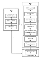
図1は、GPU向けのハードウェア強制コンテンツ保護のための本開示の技法を実装するために使用されてもよい例示的なコンピューティングデバイス2を示すブロック図である。コンピューティングデバイス2は、たとえば、パーソナルコンピュータ、デスクトップコンピュータ、ラップトップコンピュータ、タブレットコンピュータ、コンピュータワークステーション、ビデオゲームプラットフォームもしくはコンソール、たとえば、セルラー電話もしくは衛星電話などの携帯電話、固定電話、インターネット電話、いわゆるスマートフォン、ポータブルビデオゲームデバイスもしくは携帯情報端末(PDA)などのハンドヘルドデバイス、パーソナル音楽プレーヤ、ビデオプレーヤ、ディスプレイデバイス、テレビジョン、テレビジョンセットトップボックス、サーバ、中間ネットワークデバイス、メインフレームコンピュータ、任意のモバイルデバイス、またはグラフィカルデータを処理および/もしくは表示する任意の他のタイプのデバイスを含んでもよい。
FIG. 1 is a block diagram illustrating an
図1の例に示すように、コンピューティングデバイス2は、ユーザ入力インターフェース4、中央処理ユニット(CPU)6、1つまたは複数のメモリコントローラ8、システムメモリ10、グラフィックス処理ユニット(GPU)12、グラフィックスメモリ14、ディスプレイインターフェース16、ディスプレイ18、ならびにバス20および22を含んでもよい。いくつかの例では、グラフィックスメモリ14はGPU12に「オンチップ」であってもよいことに留意されたい。場合によっては、図1に示すすべてのハードウェア要素は、たとえば、システムオンチップ(SoC)設計において、オンチップであってもよい。ユーザ入力インターフェース4、CPU6、メモリコントローラ8、GPU12およびディスプレイインターフェース16は、バス20を使用して互いと通信してもよい。メモリコントローラ8およびシステムメモリ10はまた、バス22を使用して互いと通信してもよい。バス20、22は、第3世代バス(たとえば、HyperTransportバスまたはInfiniBandバス)、第2世代バス(たとえば、アドバンストグラフィックスポートバス、ペリフェラルコンポーネントインターコネクト(PCI)エクスプレスバス、もしくはアドバンストエクステンシブルインターフェース(AXI)バス)または別のタイプのバスもしくはデバイスインターコネクトなどの様々なバス構造のいずれかであってもよい。図1に示す異なる構成要素間のバスおよび通信インターフェースの特定の構成は例にすぎず、同じまたは異なる構成要素を有するコンピューティングデバイスおよび/または他のグラフィックス処理システムの他の構成が本開示の技法を実装するために使用されてもよいことに留意されたい。
As shown in the example of FIG. 1, the
CPU6は、コンピューティングデバイス2の動作を制御する汎用または専用プロセッサを備えてもよい。ユーザは、CPU6に1つまたは複数のソフトウェアアプリケーションを実行させるために、コンピューティングデバイス2に入力を与えてもよい。CPU6上で実行するソフトウェアアプリケーションは、たとえば、オペレーティングシステム、ワードプロセッサアプリケーション、電子メールアプリケーション、スプレッドシートアプリケーション、メディアプレーヤアプリケーション、ビデオゲームアプリケーション、グラフィカルユーザインターフェースアプリケーションまたは別のプログラムを含んでもよい。加えて、CPU6は、GPU12の動作を制御するためのGPUドライバ7を実行してもよい。ユーザは、ユーザ入力インターフェース4を介してコンピューティングデバイス2に結合されるキーボード、マウス、マイクロフォン、タッチパッド、タッチスクリーン、または別の入力デバイスなどの1つまたは複数の入力デバイス(図示せず)を介して、入力をコンピューティングデバイス2に与えてもよい。
The
CPU6上で実行するソフトウェアアプリケーションは、ディスプレイ18へのグラフィックスデータのレンダリングを引き起こすようCPU6に命令する1つまたは複数のグラフィックスレンダリング命令を含んでもよい。いくつかの例では、ソフトウェア命令は、たとえば、オープングラフィックスライブラリ(OpenGL(登録商標))API、オープングラフィックスライブラリ組込みシステム(OpenGL ES)API、オープンコンピューティング言語(OpenCL(登録商標))、Direct3D API、X3D API、RenderMan API、WebGL API、または任意の他の公的もしくはプロプライエタリ規格グラフィックスAPIなどのグラフィックスアプリケーションプログラミングインターフェース(API)に準拠してもよい。グラフィックスレンダリング命令を処理するために、CPU6は、GPU12にグラフィックスデータのレンダリングの一部または全部を実施させるために、1つまたは複数のグラフィックスレンダリングコマンドをGPU12に(たとえば、GPUドライバ7を通して)発行してもよい。いくつかの例では、レンダリングされるべきグラフィックスデータは、グラフィックスプリミティブ、たとえば、点、線、三角形、四角形、三角形ストリップなどのリストを含んでもよい。
A software application executing on
メモリコントローラ8は、システムメモリ10を出入りするデータの転送を容易にする。たとえば、メモリコントローラ8は、メモリ読取りコマンドおよびメモリ書込みコマンドを受け取り、メモリサービスをコンピューティングデバイス2内の構成要素に提供するためにシステムメモリ10に対してそのようなコマンドをサービスしてもよい。メモリコントローラ8は、メモリバス22を介してシステムメモリ10に通信可能に結合される。メモリコントローラ8は、CPU6とシステムメモリ10の両方とは別の処理モジュールであるものとして図1に示されているが、他の例では、メモリコントローラ8の機能性の一部または全部は、CPU6、GPU12およびシステムメモリ10のうちの1つまたはいずれかの上で実装されてもよい。システムメモリ10は、1つまたは複数のメモリユニットを備えてもよい。メモリユニットは、物理的に分割されてもよく(たとえば、別個の物理ディスクもしくはソリッドステートメモリユニット)、またはメモリアドレス範囲によって分割されてもよい。具体的には、システムメモリ10は、「セキュア」メモリユニットおよび「非セキュア」メモリユニットからなる2つ以上のメモリユニットに分割されてもよい。いくつかの例では、セキュアメモリユニットは、そこに記憶されたデータのアクセス、コピー、または解読を防止するのに、暗号化および/または他のデジタル著作権管理(DRM)技法を使用してもよい。
The memory controller 8 facilitates data transfer to and from the
メモリコントローラ8はまた、システムメモリ10へのIOデバイスアクセス(たとえば、GPU)を制御するためのIOMMU(すなわち、入出力MMU)を含む、1つまたは複数のメモリ管理ユニット(MMU)を含んでもよい。メモリ管理ユニットは、仮想メモリシステムを実装してもよい。仮想メモリ空間は、複数の仮想ページに分割されてもよい。これらの仮想ページは連続してもよいが、これらの仮想ページが対応するシステムメモリ10内の物理ページはシステムメモリ10内で連続しなくてもよい。ページは、MMUが管理することが可能であってもよい最小単位と考えられてもよい。
The memory controller 8 may also include one or more memory management units (MMUs), including an IOMMU (i.e., input / output MMU) for controlling IO device access (e.g., GPU) to the
中央処理ユニット(CPU)上で稼動する現代のオペレーティングシステム(OS)は通常、CPU上で動作する複数のプログラムにメモリを割り振るための仮想メモリ方式を使用する。仮想メモリは、アプリケーションがメモリ(すなわち、仮想メモリ)の1つのセットを参照する必要だけがあるように、コンピュータシステムの物理メモリ(たとえば、RAM、ディスクストレージなど)を仮想化するメモリ管理技法である。仮想メモリは、物理メモリ中のロケーションにマッピングされる、連続するアドレス空間からなる。このようにして、物理メモリのフラグメント化はアプリケーションから「隠され」、アプリケーションは代わりに、仮想メモリの連続するブロックと対話してもよい。仮想メモリ中の連続するブロックは通常、「ページ」に配列される。各ページは、仮想メモリアドレスのある程度の固定長の連続するブロックである。仮想メモリから物理メモリへのマッピングはしばしば、メモリ管理ユニット(MMU)によって扱われる。物理メモリ中のロケーションに現在マッピングされている仮想メモリ空間は、物理メモリに「戻される」とみなされる。 Modern operating systems (OS) that run on a central processing unit (CPU) typically use a virtual memory scheme to allocate memory to multiple programs that run on the CPU. Virtual memory is a memory management technique that virtualizes a computer system's physical memory (e.g., RAM, disk storage, etc.) so that an application only needs to reference one set of memory (i.e., virtual memory). . Virtual memory consists of a contiguous address space that is mapped to locations in physical memory. In this way, physical memory fragmentation is “hidden” from the application and the application may instead interact with successive blocks of virtual memory. Consecutive blocks in virtual memory are usually arranged in “pages”. Each page is a continuous block of a certain fixed length of virtual memory addresses. The mapping from virtual memory to physical memory is often handled by a memory management unit (MMU). Virtual memory space that is currently mapped to a location in physical memory is considered “returned” to physical memory.
仮想メモリ空間中のロケーションの物理メモリへのマッピングは、トランスレーションルックアサイドバッファ(TLB)を用いて記憶される。TLBは、MMUによって仮想アドレスを物理アドレスに素早く翻訳するのに使用される。TLBは、仮想メモリアドレスを入力として使用し、物理メモリアドレスを出力するコンテンツアドレス可能メモリ(CAM)として実装されてもよい。MMUは次いで、要求されたデータを出力物理メモリアドレスを使って素早く取り出してもよい。 The mapping of locations in virtual memory space to physical memory is stored using a translation lookaside buffer (TLB). TLB is used by the MMU to quickly translate virtual addresses into physical addresses. The TLB may be implemented as a content addressable memory (CAM) that uses a virtual memory address as input and outputs a physical memory address. The MMU may then quickly retrieve the requested data using the output physical memory address.
図2は、システムメモリ10の例示的物理ページを示す概念図である。たとえば、図2は、4つのセクション(セクション0〜3)を含む仮想ページ42を含むIOMMU40を示す。仮想ページ42は、理解しやすいように図2に示されている仮想構成物であることを理解されたい。図2において、システムメモリ10は、仮想ページ42に対応する物理ペーhジ44を含んでもよい。
FIG. 2 is a conceptual diagram illustrating an exemplary physical page of
物理ページ44は、システムメモリ10の複数のメモリユニットにわたって記憶されてもよい。たとえば、物理ページ44は、メモリユニット11Aとメモリユニット11Nの両方を包含してもよい。一例では、メモリユニット11Aは「セキュア」メモリユニットであり、メモリユニット11Nは「非セキュア」メモリユニットである。メモリユニット11Aは、部分44Aとして示される物理ページ44の一部分を記憶してもよく、メモリユニット11Nは、部分44Bとして示される物理ページ44の一部分を記憶してもよい。図示されているように、メモリユニット11Aは、物理ページ44のセクション0およびセクション2を記憶し、メモリユニット11Nは、物理ページ44のセクション1およびセクション3を記憶する。
The
図2の例は、説明のために2つのメモリユニットのみを含むが、任意の数のメモリユニットが使用されてもよい。たとえば、再び図1を参照すると、GPUドライバ7は、GPU12にピクセル値またはどの他の計算された値も記憶させる命令を伝送してもよく、ピクセル値が記憶されるところについての仮想アドレスを伝送してもよい。GPU12は、仮想アドレスに従ってピクセル値を記憶するようにIOMMU40に要求してもよい。IOMMU40は、仮想アドレスを物理アドレスにマッピングし、その物理アドレスに基づいて、インターリービング様式でシステムメモリ10のページ中にピクセル値を記憶してもよい。
The example of FIG. 2 includes only two memory units for purposes of illustration, but any number of memory units may be used. For example, referring again to FIG. 1, the
図1に戻ると、システムメモリ10は、CPU6による実行のためにアクセス可能なプログラムモジュールおよび/もしくは命令ならびに/またはCPU6上で実行するプログラムが使用するためのデータを記憶してもよい。たとえば、システムメモリ10は、ディスプレイ18上にグラフィカルユーザインターフェース(GUI)を提示するためにCPU6によって使用されるウィンドウマネージャアプリケーションを記憶してもよい。加えて、システムメモリ10は、ユーザアプリケーションと、アプリケーションに関連付けられたアプリケーションサーフェスデータとを記憶してもよい。システムメモリ10は加えて、コンピューティングデバイス2の他の構成要素が使用するための、および/またはそれらの構成要素によって生成される情報を記憶してもよい。たとえば、システムメモリ10は、GPU12用のデバイスメモリとして働いてもよく、GPU12による操作を受けるべきデータならびにGPU12によって実施された動作から生じたデータを記憶してもよい。たとえば、システムメモリ10は、DRM保護ゲームコンテンツまたはGPU12によって生じた復号ビデオを記憶してもよい。この状況において、そのようなDRM保護コンテンツは好ましくは、システムメモリ10のセキュアメモリユニット中に記憶される。他の例として、システムメモリ10は、テクスチャバッファ、デプスバッファ、ステンシルバッファ、頂点バッファ、フレームバッファなどの任意の組合せなど、他のグラフィックスデータを記憶してもよい。システムメモリ10は、たとえば、ランダムアクセスメモリ(RAM)、スタティックRAM(SRAM)、ダイナミックRAM(DRAM)、読取り専用メモリ(ROM)、消去可能プログラマブルROM(EPROM)、電気的消去可能プログラマブルROM(EEPROM)、フラッシュメモリ、磁気データ媒体または光学記憶媒体など、1つまたは複数の揮発性または不揮発性メモリまたはストレージデバイスを含んでもよい。
Returning to FIG. 1, the
GPU12は、1つまたは複数のグラフィックスプリミティブをディスプレイ18にレンダリングするためのグラフィックス演算を実施するように構成されてもよい。したがって、CPU6上で実行するソフトウェアアプリケーションのうちの1つがグラフィックス処理を必要とするとき、CPU6はディスプレイ18にレンダリングするためにグラフィックスコマンドおよびグラフィックスデータをGPU12に与えてもよい。グラフィックスデータは、たとえば、描画コマンド、状態情報、プリミティブ情報、テクスチャ情報などを含んでもよい。GPU12は、いくつかの事例では、CPU6よりも効率的な、複雑なグラフィック関連動作の処理を実現する高度並列構造で構築されてもよい。たとえば、GPU12は、複数の頂点またはピクセル上で並行して動作するように構成される複数の処理要素を含んでもよい。GPU12の高度並列の性質は、いくつかの事例では、CPU6を使用してシーンを直接ディスプレイ18に描画するよりも速く、GPU12がグラフィックス画像(たとえば、GUIならびに2次元(2D)および/または3次元(3D)グラフィックスシーン)をディスプレイ18上で描画することを可能にする場合がある。
The
GPU12は、いくつかの事例では、コンピューティングデバイス2のマザーボードに統合される場合がある。他の事例では、GPU12は、コンピューティングデバイス2のマザーボード内のポートにインストールされたグラフィックスカード上に存在してもよく、またはそうでなければコンピューティングデバイス2と相互動作するように構成される周辺デバイス内に組み込まれてもよい。GPU12は、1つもしくは複数のマイクロプロセッサ、特定用途向け集積回路(ASIC)、フィールドプログラマブルゲートアレイ(FPGA)、デジタル信号プロセッサ(DSP)、または他の等価な集積論理回路もしくはディスクリート論理回路などの1つまたは複数のプロセッサを含んでもよい。
The
GPU12は、グラフィックスメモリ14に直接結合されてもよい。したがって、GPU12は、バス20を使用することなしに、グラフィックスメモリ14からデータを読み取り、グラフィックスメモリ14にデータを書き込んでもよい。言い換えれば、GPU12は、他の、より遅いシステムメモリを使用する代わりに、ローカルストレージを使ってデータをローカルに処理してもよい。このことは、GPU12が重いバストラフィックを経る場合がある、システムバス20を介してGPU12がデータを読み書きする必要をなくすことによって、より効率的に動作することを可能にする。しかしながら、いくつかの事例では、GPU12は別個のメモリを含まないが、代わりにバス20を介してシステムメモリ10を利用する場合がある。グラフィックスメモリ14は、たとえば、ランダムアクセスメモリ(RAM)、スタティックRAM(SRAM)、ダイナミックRAM(DRAM)、消去可能プログラマブルROM(EPROM)、電気的消去可能プログラマブルROM(EEPROM)、フラッシュメモリ、磁気データ媒体または光学記憶媒体など、1つまたは複数の揮発性または不揮発性メモリまたはストレージデバイスを含んでもよい。
The
CPU6および/またはGPU12は、レンダリングされた画像データをフレームバッファ15に記憶してもよい。通常、フレームバッファ15は、システムメモリ10内で割り振られることになるが、いくつかの状況では独立メモリであってもよい。ディスプレイインターフェース16は、フレームバッファ15からデータを取り出し、レンダリングされた画像データによって表される画像を表示するようにディスプレイ18を構成してもよい。いくつかの例では、ディスプレイインターフェース16は、フレームバッファから取り出されたデジタル値をディスプレイ18が消費できるアナログ信号にコンバートするように構成されるデジタルアナログコンバータ(DAC)を含んでもよい。他の例では、ディスプレイインターフェース16は、処理のためにデジタル値を直接ディスプレイ18に渡してもよい。ディスプレイ18は、モニタ、テレビジョン、投影デバイス、液晶ディスプレイ(LCD)、プラズマディスプレイパネル、有機LED(OLED)ディスプレイなどの発光ダイオード(LED)アレイ、陰極線管(CRT)ディスプレイ、電子ペーパー、表面伝導電子放出ディスプレイ(SED)、レーザーテレビジョンディスプレイ、ナノ結晶ディスプレイまたは別のタイプのディスプレイユニットを含んでもよい。ディスプレイ18は、コンピューティングデバイス2内に統合されてもよい。たとえば、ディスプレイ18は、携帯電話またはタブレットコンピュータのスクリーンであってもよい。代替的に、ディスプレイ18は、ワイヤードまたはワイヤレス通信リンクを介してコンピューティングデバイス2に結合されるスタンドアロンデバイスであってもよい。たとえば、ディスプレイ18は、ケーブルまたはワイヤレスリンクを介してパーソナルコンピュータに接続されるコンピュータモニタまたはフラットパネルディスプレイであってもよい。
The
図3は、図1のCPU6、GPU12、およびシステムメモリ10の例示的な実装形態をさらに詳細に示すブロック図である。CPU6は、少なくとも1つのソフトウェアアプリケーション24、グラフィックスAPI26、およびGPUドライバ7を含んでもよく、これらの各々は、CPU6上で実行する1つまたは複数のソフトウェアアプリケーションまたはサービスであってもよい。GPU12は、グラフィックス処理コマンドを実行するために一緒に動作する複数のグラフィックス処理ステージを含む3Dグラフィックス処理パイプライン30を含んでもよい。GPU12は、ビニングレンダリングモードおよび直接レンダリングモード(タイルベースまたは遅延レンダリングモードとも呼ばれる)を含む様々なレンダリングモードでグラフィックス処理パイプライン30を実行するように構成されてもよい。GPU12はまた、GPUハードウェアの高度並列の性質によって実行されるように適用可能なより一般的な計算を実施するための汎用シェーダ39を実行するように動作可能であってもよい。そのような汎用アプリケーションは、いわゆる汎用グラフィックス処理ユニット(GPGPU)であってもよく、OpenCLなどの汎用APIに準拠する場合がある。
FIG. 3 is a block diagram illustrating in greater detail an exemplary implementation of
図3に示すように、グラフィックス処理パイプライン30は、コマンドエンジン32、ジオメトリ処理ステージ34、ラスタ化ステージ36、およびピクセル処理パイプライン38を含んでもよい。グラフィックス処理パイプライン30中の構成要素の各々は、固定機能構成要素、(たとえば、プログラマブルシェーダユニット上で実行するシェーダプログラムの一部としての)プログラマブル構成要素として、または固定機能構成要素とプログラマブル構成要素の組合せとして実装されてもよい。CPU6およびGPU12が利用可能なメモリは、それ自体がフレームバッファ15を含む場合があるシステムメモリ10を含んでもよい。フレームバッファ15は、レンダリングされた画像データを記憶してもよい。
As shown in FIG. 3,
ソフトウェアアプリケーション24は、GPU12の機能性を利用する任意のアプリケーションであってもよい。たとえば、ソフトウェアアプリケーション24は、GUIアプリケーション、オペレーティングシステム、ポータブルマッピングアプリケーション、エンジニアリングもしくは美術アプリケーション用のコンピュータ支援設計プログラム、ビデオゲームアプリケーション、または2Dもしくは3Dグラフィックスを使用する別のタイプのソフトウェアアプリケーションであってもよい。ソフトウェアアプリケーション24はまた、たとえばGPGPUアプリケーションにおいて、より全般的な計算を実施するのにGPUを使用するアプリケーションであってもよい。
The software application 24 may be any application that uses the functionality of the
ソフトウェアアプリケーション24は、グラフィカルユーザインターフェース(GUI)および/またはグラフィックスシーンをレンダリングするようGPU12に命令する1つまたは複数の描画命令を含んでもよい。たとえば、描画命令は、GPU12によってレンダリングされるべき1つまたは複数のグラフィックスプリミティブのセットを定義する命令を含んでもよい。いくつかの例では、描画命令は、GUIで使用される複数のウィンドウ処理サーフェスの全部または一部をまとめて定義してもよい。追加の例では、描画命令は、アプリケーションによって定義されたモデル空間またはワールド空間内に1つまたは複数のグラフィックスオブジェクトを含むグラフィックスシーンの全部または一部をまとめて定義してもよい。
The software application 24 may include a graphical user interface (GUI) and / or one or more drawing instructions that instruct the
ソフトウェアアプリケーション24は、1つまたは複数のグラフィックスプリミティブを表示可能なグラフィックス画像にレンダリングするための1つまたは複数のコマンドをGPU12に発行するために、グラフィックスAPI26を介してGPUドライバ7を呼び出す場合がある。たとえば、ソフトウェアアプリケーション24は、プリミティブ定義をGPU12に与えるために、グラフィックスAPI26を介してGPUドライバ7を呼び出す場合がある。いくつかの事例では、プリミティブ定義は、描画プリミティブ、たとえば、三角形、矩形、三角形ファン、三角形ストリップなどのリストの形でGPU12に与えられる場合がある。プリミティブ定義は、レンダリングされるべきプリミティブに関連付けられた1つまたは複数の頂点を指定する頂点仕様を含んでもよい。頂点仕様は、頂点ごとの位置座標と、いくつかの事例では、たとえば、色座標、法線ベクトル、およびテクスチャ座標など、頂点に関連付けられた他の属性とを含んでもよい。プリミティブ定義はまた、プリミティブタイプ情報(たとえば、三角形、矩形、三角形ファン、三角形ストリップなど)、スケーリング情報、回転情報などを含んでもよい。ソフトウェアアプリケーション24によってGPUドライバ7に発行された命令に基づいて、GPUドライバ7は、プリミティブをレンダリングするためにGPU12が実施する1つまたは複数の動作を指定する1つまたは複数のコマンドを公式化する場合がある。GPU12がCPU6からコマンドを受け取ると、グラフィックス処理パイプライン30は、コマンドを復号し、コマンドにおいて指定された動作を実施するようにグラフィックス処理パイプライン30内の1つまたは複数の処理要素を構成する。指定された動作を実施した後、グラフィックス処理パイプライン30は、レンダリングされたデータをディスプレイデバイスに関連付けられたフレームバッファ15に出力する。グラフィックス処理パイプライン30は、ビニングレンダリングモードおよび直接レンダリングモードを含む複数の異なるレンダリングモードのうちの1つで実行するように構成されてもよい。
Software application 24 calls
GPUドライバ7は、1つまたは複数のシェーダプログラムをコンパイルし、コンパイルされたシェーダプログラムをGPU12内に含まれる1つまたは複数のプログラマブルシェーダユニットにダウンロードするようにさらに構成されてもよい。シェーダプログラムは、たとえば、OpenGL Shading Language(GLSL)、High Level Shading Language(HLSL)、C for Graphics(Cg) shading languageなどの高レベルシェーディング言語で書かれる場合がある。コンパイルされたシェーダプログラムは、GPU12内のプログラマブルシェーダユニットの動作を制御する1つまたは複数の命令を含んでもよい。たとえば、シェーダプログラムは、頂点シェーダプログラムおよび/またはピクセルシェーダプログラムを含んでもよい。頂点シェーダプログラムは、プログラマブル頂点シェーダユニットまたはユニファイドシェーダユニットの実行を制御し、1つまたは複数の頂点ごとの動作を指定する命令を含んでもよい。ピクセルシェーダプログラムは、プログラマブルピクセルシェーダユニットまたはユニファイドシェーダユニットの実行を制御するピクセルシェーダプログラムを含み、1つまたは複数のピクセルごとの動作を指定する命令を含んでもよい。本開示のいくつかの例によれば、ピクセルシェーダプログラムはまた、ソースピクセルについてのテクスチャ値を、それらのソースピクセルについての対応する宛先アルファ値に基づいて選択的に取り出させる命令を含んでもよい。
The
グラフィックス処理パイプライン30は、グラフィックスドライバ7を介してCPU6から1つまたは複数のグラフィックス処理コマンドを受け取り、表示可能なグラフィックス画像を生成するためのグラフィックス処理コマンドを実行するように構成されてもよい。上記で説明したように、グラフィックス処理パイプライン30は、グラフィックス処理コマンドを実行するために一緒に動作する複数のステージを含む。しかしながら、そのようなステージは必ずしも別個のハードウェアブロックにおいて実装される必要はないことに留意されたい。たとえば、ジオメトリ処理ステージ34およびピクセル処理パイプライン38の部分は、ユニファイドシェーダユニットの一部として実装されてもよい。やはり、グラフィックス処理パイプライン30は、ビニングレンダリングモードおよび直接レンダリングモードを含む複数の異なるレンダリングモードのうちの1つで実行するように構成されてもよい。
The
コマンドエンジン32は、グラフィックス処理コマンドを受信し、グラフィックス処理コマンドを実践するための様々な動作を実施するようにグラフィックス処理パイプライン30内の残りの処理ステージを構成してもよい。グラフィックス処理コマンドは、たとえば、描画コマンドおよびグラフィックス状態コマンドを含んでもよい。描画コマンドは、1つまたは複数の頂点の位置座標と、いくつかの事例では、たとえば、色座標、法線ベクトル、テクスチャ座標およびかぶり座標など、頂点の各々に関連付けられた他の属性値とを指定する頂点仕様コマンドを含んでもよい。グラフィックス状態コマンドは、プリミティブタイプコマンド、変換コマンド、照明コマンドなどを含んでもよい。プリミティブタイプコマンドは、レンダリングされるべきプリミティブのタイプおよび/またはプリミティブを形成するために頂点がどのように組み合わされるかを指定してもよい。変換コマンドは、頂点に対して実施すべき変換のタイプを指定してもよい。照明コマンドは、グラフィックスシーン内の異なる照明のタイプ、方向および/または配置を指定してもよい。コマンドエンジン32は、ジオメトリ処理ステージ34に、1つまたは複数の受信されたコマンドに関連付けられた頂点および/またはプリミティブに対してジオメトリ処理を実施させる場合がある。
The command engine 32 may receive the graphics processing command and configure the remaining processing stages in the
ジオメトリ処理ステージ34は、ラスタ化ステージ36のためのプリミティブデータを生成するために、1つまたは複数の頂点に対して頂点ごとの動作および/またはプリミティブセットアップ動作を実施してもよい。各頂点は、たとえば、位置座標、色値、法線ベクトル、およびテクスチャ座標などの属性のセットに関連付けられてもよい。ジオメトリ処理ステージ34は、様々な頂点ごとの動作に従って、これらの属性のうちの1つまたは複数を修正する。たとえば、ジオメトリ処理ステージ34は、修正された頂点位置座標を生成するために、頂点位置座標に対して1つまたは複数の変換を実施してもよい。ジオメトリ処理ステージ34は、修正された頂点位置座標を生成するために、たとえば、モデリング変換、ビューイング変換、投影変換、モデルビュー(ModelView)変換、モデルビュー投影(ModelViewProjection)変換、ビューポート変換およびデプス範囲スケーリング変換のうちの1つまたは複数を頂点位置座標に適用してもよい。いくつかの事例では、頂点位置座標はモデル空間座標であってもよく、修正された頂点位置座標はスクリーン空間座標であってもよい。スクリーン空間座標は、モデリング変換、ビューイング変換、投影変換およびビューポート変換の適用の後で取得されてもよい。いくつかの事例では、ジオメトリ処理ステージ34はまた、頂点の修正された色座標を生成するために、頂点に対して頂点ごとの照明動作を実施してもよい。ジオメトリ処理ステージ34はまた、たとえば、正規変換、ノーマル正規化動作(normal normalization operations)、ビューボリュームクリッピング、同次除算動作および/またはバックフェースカリング動作を含む他の動作を実施してもよい。
ジオメトリ処理ステージ34は、ラスタ化されるべきプリミティブを定義する1つまたは複数の修正された頂点のセットを含むプリミティブデータ、ならびにプリミティブを形成するために頂点がどのように組み合わされるかを指定するデータを生成してもよい。修正された頂点の各々は、たとえば、修正された頂点位置座標と、頂点に関連付けられた処理された頂点属性値とを含んでもよい。プリミティブデータはまとめて、グラフィックス処理パイプライン30のさらなるステージによってラスタ化されるべきプリミティブに対応する場合がある。概念的には、各頂点は、プリミティブの2つの辺がぶつかるプリミティブの角に対応する場合がある。ジオメトリ処理ステージ34は、さらなる処理のためにプリミティブデータをラスタ化ステージ36に与えてもよい。
いくつかの例では、ジオメトリ処理ステージ34の全部または一部が、1つまたは複数のシェーダユニット上で実行する1つまたは複数のシェーダプログラムによって実装される場合がある。たとえば、ジオメトリ処理ステージ34は、そのような例では、頂点シェーダ、ジオメトリシェーダまたはそれらの任意の組合せによって実装される場合がある。他の例では、ジオメトリ処理ステージ34は、固定機能ハードウェア処理パイプラインとして、または固定機能ハードウェアと1つもしくは複数のシェーダユニット上で実行する1つもしくは複数のシェーダプログラムの組合せとして実装される場合がある。
In some examples, all or part of the
ラスタ化ステージ36は、ジオメトリ処理ステージ34から、ラスタ化されるべきプリミティブを表すプリミティブデータを受信し、プリミティブをラスタ化して、ラスタ化されたプリミティブに対応する複数のソースピクセルを生成するように構成される。いくつかの例では、ラスタ化ステージ36は、どのスクリーンピクセルロケーションがラスタ化されるべきプリミティブによってカバーされるかを決定し、プリミティブによってカバーされると決定されたスクリーンピクセルロケーションごとのソースピクセルを生成してもよい。ラスタ化ステージ36は、たとえば、エッジウォーキング(edge-walking)技法、エッジ方程式評価(evaluating edge equations)などの、当業者に知られている技法を使用することによって、どのスクリーンピクセルロケーションがプリミティブによってカバーされるかを決定してもよい。ラスタ化ステージ36は、さらなる処理のために、得られたソースピクセルをピクセル処理パイプライン38に与えてもよい。
ラスタ化ステージ36によって生成されたソースピクセルは、スクリーンピクセルロケーション、たとえば、宛先ピクセルに対応し、1つまたは複数の色属性に関連付けられる場合がある。特定のラスタ化されたプリミティブのために生成されたソースピクセルのすべては、ラスタ化されたプリミティブに関連付けられていると言える。プリミティブによってカバーされるべき、ラスタ化ステージ36によって決定されたピクセルは、概念的には、プリミティブの頂点を表すピクセル、プリミティブの辺を表すピクセル、およびプリミティブの内部を表すピクセルを含んでもよい。
The source pixel generated by the
ピクセル処理パイプライン38は、ラスタ化されたプリミティブに関連付けられたソースピクセルを受信し、ソースピクセルに対して1つまたは複数のピクセルごとの動作を実施するように構成される。ピクセル処理パイプライン38によって実施される場合があるピクセルごとの動作は、たとえば、アルファテスト、テクスチャマッピング、色計算、ピクセルシェーディング、ピクセルごとの照明、かぶり処理、ブレンディング、ピクセルオーナーシップテキスト、ソースアルファテスト、ステンシルテスト、デプステスト、シザーテストおよび/またはスティップリング動作を含む。加えて、ピクセル処理パイプライン38は、1つまたは複数のピクセルごとの動作を実施するための1つまたは複数のピクセルシェーダプログラムを実行してもよい。ピクセル処理パイプライン38によって生成された得られたデータは、本明細書では宛先ピクセルデータと呼ばれ、フレームバッファ15に記憶される場合がある。宛先ピクセルデータは、処理されたソースピクセルと同じ表示ロケーションを有する、フレームバッファ15内の宛先ピクセルに関連付けられる場合がある。宛先ピクセルデータは、たとえば、色値、宛先アルファ値、デプス値などのデータを含んでもよい。
フレームバッファ15は、GPU12のための宛先ピクセルを記憶する。各宛先ピクセルは、一意のスクリーンピクセルロケーションに関連付けられる場合がある。いくつかの例では、フレームバッファ15は、宛先ピクセルごとの色成分および宛先アルファ値を記憶してもよい。たとえば、フレームバッファ15はピクセルごとの赤(Red)、緑(Green)、青(Blue)、アルファ(Alpha)(RGBA)成分を記憶してもよく、"RGB"成分は色値に対応し、"A"成分は宛先アルファ値に対応する。ピクセル値はまた、ルーマ成分(Y)ならびに1つまたは複数のクロマ成分(たとえば、UおよびV)で表されてもよい。フレームバッファ15およびシステムメモリ10は別個のメモリユニットであるものとして示されているが、他の例では、フレームバッファ15はシステムメモリ10の一部であってもよい。
The
汎用シェーダ39は、計算を実施するようにGPU12上で実行可能な、どのアプリケーションであってもよい。通常、そのような計算は、算術論理ユニット(ALU)を含む、GPU処理コアの高度並列構造を利用するタイプである。例示的汎用シェーダ39は、OpenCL APIに準拠してもよい。OpenCLは、アプリケーションが、異種システム(たとえば、CPU、GPU、DSPなど)を含むシステムにおいて複数のプロセッサにわたってアクセスを有することができるようにするAPIである。通常、OpenCLに準拠するアプリケーションにおいて、GPU12は、非グラフィカルコンピューティングを実施するのに使用されることになる。非グラフィカルコンピューティングアプリケーションの例は、特に、物理ベースのシミュレーション、高速フーリエ変換、オーディオ信号処理、デジタル画像処理、ビデオ処理、画像ポストフィルタリング、コンピュテーショナルカメラ、気候研究、天気予報、ニューラルネットワーク、暗号技術、および超並列データクランチングを含み得る。
The
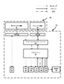
図4は、本開示のハードウェア強制コンテンツ保護技法を実装するように構成される例示的なデバイスを示すブロック図である。図4の例では、GPU12は、セキュアモードまたは非セキュアモードに従って動作するように構成されてもよい。本開示の一例では、セキュアモードでは、GPU12は、出力データ(たとえば、ゲームデータ、ビデオなど)を非セキュアメモリ56に書き込むことを制限される。そうではなく、セキュアモードでは、GPU12は、セキュアメモリ57に出力データを書き込むことしかできない。セキュアモードにある間、GPU12は、セキュアメモリ57または非セキュアメモリ56のいずれかからデータを読み取ってもよい。非セキュアモードにおいて、この例では、GPU12は、セキュアメモリ57からどのデータを読み取ることも制限される。むしろ、非セキュアモードでは、GPU12は、非セキュアメモリ56からデータを読み取ることしかできない。同様に、非セキュアモードにある間、GPU12は、非セキュアメモリ56にデータを書き込むことしかできない。
FIG. 4 is a block diagram illustrating an example device configured to implement the hardware-enforced content protection techniques of this disclosure. In the example of FIG. 4, the
非セキュアメモリ56およびセキュアメモリ57は、1つまたは複数の揮発性または不揮発性メモリまたは記憶デバイスを含む、どのタイプのメモリであってもよい。例示的メモリおよび記憶デバイスは、RAM、SRAM、DRAM、ROM、EPROM、EEPROM、フラッシュメモリ、磁気データ媒体または光学記憶媒体を含む。セキュアメモリ57は、非セキュアメモリ56には見られない追加特徴を含む。たとえば、セキュアメモリ57は、そこに記憶されたデータへのアクセス、コピー、または解読を防止するのに、暗号化、認証および/または他のデジタル著作権管理技法を使用してもよい。概して、セキュアメモリ57は、システムメモリ10の一部分であるとみなされてもよく、非セキュアメモリ56は、システムメモリ10の別の部分であるとみなされてもよい。
以下で説明する本開示の1つまたは複数の例によると、GPU12は、メモリアクセスコントローラ53を使って、データがどこから読み取られ、どこに書き込まれるかを制御し、またはそうでなければ影響を与えるように構成されてもよい。メモリアクセスコントローラ53は、GPU12が動作しているモード(すなわち、セキュアモードまたは非セキュアモード)に応答し、モードに基づいて読取り/書込み決定を行う。概して、メモリアクセスコントローラ53は、GPU12とメモリコントローラ50との間のトランザクションの性質に制約を課すように構成されてもよい。メモリアクセスコントローラ53は、GPU12が現在動作しているモード(すなわち、セキュアモードまたは非セキュアモード)に応答するように構成されてもよく、以下の本開示の例に従って、メモリトランザクションに制約を課してもよい。
According to one or more examples of the present disclosure described below, the
本開示の一例では、GPUメモリモード(たとえば、セキュアモードまたは非セキュアモード)は、CPU6上で動作するGPUドライバ7によってセットされる。GPUドライバ7は、GPU12におけるメモリモードを、いくつかの異なるやり方で変えてもよい。一例では、GPUドライバ7は、どのメモリモードを使用するべきか(たとえば、セキュアモードまたは非セキュアモード)をGPU12に対して示す値を、GPU12中のレジスタに直接書き込んでもよい。別の例では、GPU12は、どのメモリモードを使用するべきかを示す特定の値をレジスタに書き込むようGPU12自体に命令する、GPU12によって実行可能な1つまたは複数の命令をコマンドストリーム中に含んでもよい。このようにして、GPUドライバ7は、GPUが動作するメモリモードを選択するだけでもよく、どのデータがどのメモリに書き込まれるべきかを指定する、いかなる直接命令も行わない。したがって、GPUドライバ7が、GPU12を非セキュアモードに置くように変更された場合であっても、メモリアクセスコントローラ53の機能を通して、GPU12は、セキュアメモリ57からのどの読取りアクセスも防止することになり、それは、メモリアクセスコントローラ53は、非セキュアモードでは非セキュアメモリ56から読み取ることだけが可能だからである。同様に、GPUドライバ7が、GPU12をセキュアモードに置くように変更された場合であっても、メモリアクセスコントローラ53の機能を通して、GPU12は、非セキュアメモリ56へのどの書込みアクセスも防止することになり、それは、メモリアクセスコントローラ53は、セキュアモードではセキュアメモリ57に書き込むことだけが可能だからである。したがって、本開示の技法は依然として、GPUドライバ7がGPU12をセキュアモードに置くように変更された場合であっても、非セキュアメモリ56へのデータのコピーを防止する場合がある。
In an example of the present disclosure, the GPU memory mode (eg, secure mode or non-secure mode) is set by the
本開示の一例では、メモリアクセスコントローラ53は、それぞれ、セキュアおよび非セキュアメモリ管理ユニット(MMU)ページテーブルを介してセキュアメモリ57および非セキュアメモリ56にアクセスするように構成される。この例では、GPUドライバ7によって、GPU12に仮想アドレス範囲が与えられる。仮想アドレス範囲は、セキュアメモリ用の仮想アドレスの範囲および非セキュアメモリ用の仮想アドレスの範囲を含む。GPUドライバ7によってセキュアモードに置かれているとき、GPU12は、読取りおよび書込みを実施するのに、セキュアメモリ用の仮想アドレスの範囲を使用する。GPU12はまた、セキュアモードにおいて読取りを実施するのに、ただし書込みは実施しないように、非セキュアメモリ用の仮想アドレスの範囲を使用することが可能であり、そうすることによって、セキュアメモリからの、保護データの無許可コピーを防止する。GPUドライバ7によって非セキュアモードに置かれているとき、GPU12は、読取りおよび書込みを実施するのに、非セキュアメモリ用の仮想アドレスの範囲を使用することになる。
In one example of the present disclosure, the
一例では、メモリアクセスコントローラ53は、読取りまたは書込み要求中で使用される仮想アドレスが仮想メモリアドレスの非セキュア範囲内にあるか、または仮想アドレスのセキュア範囲内にあるか判断することによって、読取りおよび書込みを適切なメモリユニット(たとえば、セキュアメモリ57または非セキュアメモリ56)にルーティングする。範囲判断に基づいて、メモリアクセスコントローラは、メモリコントローラ50中の非セキュアIOMMU51またはセキュアIOMMU52のうちの1つを使用する。メモリコントローラ50は、システムメモリ10を出入りするデータの転送を容易にするように構成される。いかなるそのようなトランザクションも効果的に扱うために、メモリコントローラ50は、システムメモリ10への、GPU12などのデバイスアクセスを制御するための1つまたは複数のMMUを含んでもよい。非セキュアIOMMU51およびセキュアIOMMU52は、そのクライアントにページの連続閲覧を提供する、仮想化メモリアドレスのためのマッピングを含む。この例では、クライアントは、1つまたは複数のリソースをバインドし、またはGPU12に提供する、どのエンティティ(たとえば、GPU12によって実行されるアプリケーションまたはCPU6上で実行するアプリケーション)であってもよい。リソースとは、GPU12が何らかのやり方で使用するための情報のコンテナ(たとえば、メモリまたはバッファ)である。いくつかの例では、リソースは、メモリがどのように使用されるべきかについての情報を提供する記述子を有してもよい。
In one example, the
本開示の一例では、非セキュアIOMMU51は、非セキュアメモリ56中で仮想メモリアドレスを物理メモリアドレスにマッピングするように構成されているIOMMUである。セキュアIOMMU52は、セキュアメモリ57中で仮想メモリアドレスを物理メモリアドレスにマッピングするように構成されているIOMMUである。非セキュアIOMMU51は、非セキュアページテーブルを使って、非セキュアメモリ56へのマッピングを実施する。非セキュアページテーブルは、仮想メモリアドレスの範囲(たとえば、GPUドライバ7によって与えられる範囲)を非セキュアメモリ56中のロケーションにマッピングするページテーブルである。同様に、セキュアIOMMU52は、セキュアページテーブルを使って、セキュアメモリ57へのマッピングを実施する。セキュアページテーブルは、仮想メモリアドレスの範囲(たとえば、GPUドライバ7によって与えられる範囲)をセキュアメモリ57中のロケーションにマッピングするページテーブルである。図4に示すように、非セキュアIOMMU51およびセキュアIOMMU52は、単一のメモリコントローラ50の一部である。メモリコントローラ50は、図1に示すメモリコントローラ8のうちの1つであってもよい。実際、メモリコントローラ50は、セキュアページテーブルを用いて動作しているときはセキュアIOMMUになり、非セキュアページテーブルを用いて動作しているときは非セキュアIOMMUになる。他の例では、非セキュアIOMMU51およびセキュアIOMMU52は、物理的に別個のMMUであってもよい。
In an example of the present disclosure, the
本開示の一例では、セキュアおよび非セキュアページテーブルの両方が、CPU6上で実行するセキュアオペレーティングシステム(OS)54によって、セキュアIOMMU52および非セキュアIOMMU51に与えられる。セキュアOSとは、通常の「リッチ」OS(たとえば、Apple iOS、Google Android、Microsoft Windowsなど)とともに動作するOSである。セキュアOSは、セキュアカーネルおよびどのセキュア周辺装置(たとえば、セキュアIOMMU52)も保護し、リッチOS上で稼動するどのコード(たとえば、GPUドライバ7)からも分離するためのセキュリティアプリケーションを提供する。セキュアOSの例が、ARM Holdings製のTrustZoneソフトウェアである。概して、セキュアOSは、グラフィックスドライバなどのソフトウェアを含む、リッチOS上で稼動するソフトウェアよりも変更および攻撃をはるかに受けにくいとみなされる。本開示の技法によると、セキュアOSのみが、仮想メモリアドレス範囲を物理メモリアドレスにマッピングするためのページテーブルを更新することを許可される。したがって、ドライバによって与えられる仮想アドレス範囲を含むグラフィックスドライバを変更するためのどの試みも、セキュアコンテンツが非セキュアメモリに記憶される結果とはならず、それは、セキュアOSのみが、セキュアおよび非セキュアメモリへの最終的マッピングを提供するからである。
In one example of the present disclosure, both secure and non-secure page tables are provided to the
セキュアおよび非セキュアページテーブルの両方がメモリコントローラ50において利用可能である(たとえば、メモリコントローラ50が、非セキュアIOMMU51とセキュアIOMMU52の両方を含む)例では、GPU12は、セキュアモードにおいて、非セキュアメモリ56とセキュアメモリ57の両方からデータを読み取ることが可能である。他の読取り/書込み制約が、依然としてあてはまる。つまり、セキュアモードでは、書込みは、GPU12によってセキュアメモリ57に対して行われるだけであり、非セキュアモードでは、GPU12による読取りと書込みの両方が、非セキュアメモリ56に限られる。
In the example where both secure and non-secure page tables are available in the memory controller 50 (e.g., the
本開示の別の例では、データトラフィックが、メモリアクセスコントローラ53を介してセキュアまたは非セキュアIOMMUのいずれかに向けられる場合、セキュアおよび非セキュアIOMMUの両方をGPUにとって利用可能にするのではなく、ただ1つのIOMMU(すなわち、非セキュアIOMMU51またはセキュアIOMMU52のいずれか)が、選択されたメモリモードに依存して、GPU12にとって利用可能にされることになる。つまり、メモリモードが非セキュアモードである場合、セキュアOS54は、非セキュアIOMMU51にページテーブルマッピングを提供するだけである。この状況において、セキュアIOMMU52は利用不可能になる。メモリモードがセキュアモードである場合、セキュアOS54は、セキュアIOMMU52にページテーブルマッピングを提供するだけである。この状況において、非セキュアIOMMU51は利用不可能になる。メモリモードごとに1つのIOMMUのみを利用可能にするこの例は、メモリモードごとに読取りと書込みの両方が制限されたより単純な実装形態を提供する。つまり、セキュアモードでは、GPU12による、セキュアメモリ57に対する読取りおよび書込みのみが許可され、非セキュアモードでは、GPU12による、非セキュアメモリ56に対する読取りおよび書込みのみが許可される。これは、セキュアモードが非セキュアメモリ56向けの読取りをそれ以上許可しないという点で、両方のIOMMUが利用可能であってもよい、上述した手法とはわずかに異なる。
In another example of the present disclosure, if data traffic is directed to either a secure or non-secure IOMMU via the
セキュアモードにあるときであっても、GPU12の最終出力産物以外の、いくつかの書込みがあり、これらは、GPUが非セキュアメモリに書き込むためにより優れている。これらの書込みは、GPU12とグラフィックスドライバ7との間の通信トークンを含む。そのようなデータは、タイムスタンプと、カウンタデータおよび照会データなど、他の補助データおよび制御データとを含む。GPU12は、そのようなタイムスタンプおよびデータをドライバに通信するのに、メモリ(たとえば、非セキュアメモリ56)を使用する。グラフィックスドライバ7は信頼できないので、通信経路に関わるメモリは、非セキュアである必要がある(たとえば、非セキュアメモリ56)。一例として、GPU12が、処理におけるある特定の地点に達すると、GPU12は、タイムスタンプ/順序マーカをメモリに書き込む。グラフィックスドライバ7は、この情報を、GPUが特定のコマンドストリーム中でどれだけ進んだかを判断するのに使用する。この判断は、たとえば、GPU12が終了すると、グラフィックスドライバ7が、GPU12がその上で動作しているメモリオブジェクトを解放できるようにする。グラフィックスドライバ7に情報を提供するためにGPU12が使ってもよい多くの他のタイプのシグナリングおよび通信経路がある。別の例として、グラフィックスドライバ7は、GPU12に、描画コールの後で実施カウンタを報告するよう要求することができる。GPU12は次いで、これらの実施カウンタを、グラフィックスドライバ7によって指定された(たとえば、非セキュアメモリ56中の)記憶ロケーションに書き込む。
Even when in secure mode, there are some writes other than the final output product of
GPU12が、セキュアモードでは非セキュアメモリに書き込まないという、上記の一般規則に対するこの例外を解消するために、GPU12ハードウェアは、いくつかのハードウェアブロックが、GPUがセキュアモードで稼動しているときにセキュアコンテンツに接続するか、またはセキュアコンテンツを含むデータ経路およびキャッシュへのアクセスをやはり有さないまま、非セキュアメモリアクセスを有するように構成されるように修正されてもよい。 In order to eliminate this exception to the general rule above that GPU12 does not write to non-secure memory in secure mode, GPU12 hardware can have several hardware blocks when the GPU is running in secure mode. It may be modified to connect to secure content or to be configured to have non-secure memory access while still having no access to data paths and caches containing secure content.
図5は、GPU12のいくつかのハードウェアブロックが、GPU12がセキュアモードにあるときであっても、GPU12のメモリインターフェースブロック(VBIF60)を通して、次いで、非セキュアIOMMU51を通して、非セキュアメモリへの直接アクセスのみを有する例示的実装形態を示す。そのようなハードウェアブロックの一例が、GPUのフロントエンドにあるコマンドプロセッサ(CP)62ブロックである。CP62は、図3に示すコマンドエンジン32などのコマンドエンジンを実行してもよい。CP62は、メッセージを(非セキュアメモリを介して)GPUドライバ7に送信することを担当する。図5に示すように、CP62は、非セキュアIOMMU51を通る、メモリ(この場合、非セキュアメモリ)へのただ1つの物理経路を有するように構成される。したがって、GPU12の他の任意のハードウェアブロックがセキュアコンテンツ上で動作しているかどうかにかかわらず、CP62は、そのようなセキュアコンテンツへのアクセスを得ることはない。CP62がセキュアコンテンツへのアクセスを有さないことをさらに確実にするために、CP62はまた、デバッグバスを含む、セキュアコンテンツを記憶するのに使用される場合があるどのレジスタからも物理的に隔離されてもよい(たとえば、どのレジスタへの接続も有さない)。図5に示すように、CP62は、L2キャッシュ61およびグラフィックスメモリ(GMEM)70への直接アクセスを有さない。GMEM70は、GPU12がGPU12のいくつかの動作モードにおいて表示するためにコンテンツをレンダリングするときにレンダターゲットまたはフレームバッファとして使用する高速メモリ(しばしば、SRAM)である。L2キャッシュ61は、メインメモリ(たとえば、セキュアメモリ)へのアクセスの数が削減されてもよいように、最近アドレス指定されたデータまたは頻繁に使用されるデータを記憶するのに使用される2次キャッシュである。L2キャッシュ61はまた、プログラム命令をバッファリングするのに使用されてもよい。通常、L2キャッシュ61はGMEM70よりも大きい。
Figure 5 shows that some hardware blocks of GPU12 only have direct access to non-secure memory through GPU12's memory interface block (VBIF60) and then through non-secure IOMMU51 even when GPU12 is in secure mode. 2 illustrates an exemplary implementation having An example of such a hardware block is a command processor (CP) 62 block at the front end of the GPU. The
GPU12の他のハードウェアブロックはまた、非セキュアメモリへのアクセスのみを有するように構成されてもよい。たとえば、プリミティブ制御(PC)ユニットおよび可視性ストリーム圧縮器(VSC)が、非セキュアメモリへのアクセスのみを有するように構成されてもよい。PCユニットが、プリミティブ(たとえば、三角形)がグラフィックスパイプライン(たとえば、図3のグラフィックス3D処理パイプライン30)を通ってどのように進行し、または「歩く」かを制御する。VSCは、タイルベースまたは遅延レンダリング方式において、可視性ストリームを圧縮し、管理するのに使用される。概して、いくつかの状況では、いくつかのハードウェアブロックに対して、セキュアメモリに書き込むよう求めるのを避けることが有益な場合がある。そのような状況は、ハードウェアブロックがセキュアコンテンツを書き込んでいない状況、およびハードウェアブロックが、グラフィックスドライバによって必要とされる制御データを書き込んでいるときを含む。
Other hardware blocks of the
図5の他のハードウェアブロックは、上述した技法に基づいて、非セキュアメモリまたはセキュアメモリにコンテンツを記憶する。つまり、非セキュアモードでは、データは、非セキュアメモリから読み取られるか、またはそこに書き込まれるだけであってもよい。どのデータも、非セキュアモードではセキュアメモリから読み取られなくてもよい。セキュアモードでは、データは、セキュアメモリに書き込まれるだけであってもよい。どのデータも、セキュアモードでは非セキュアメモリに書き込まれなくてもよい。ただし、いくつかの例におけるセキュアモードでは、データは、セキュアメモリと非セキュアメモリの両方から読み取られる場合がある。メモリモードに従ってメモリにアクセスしてもよいGPU12のこれらの追加ハードウェアブロックは、頂点フェッチ復号(VFD)ユニット65、高レベルシーケンサ(HLSQ)66、頂点シェーダ(VS)67、ピクセルシェーダ(PS)68、およびレンダバックエンド(RB)69を含む。VFD65は、CP62の要求により、頂点データをフェッチすることを担当する。HLSQ66は、シェーダプロセッサ(すなわち、シェーダコードを実行する、GPU上のプログラム可能プロセッサ)を制御して、実行されるジョブおよび起動ジョブについての正しい状態をシェーダプロセッサに投入する。VS67は、シェーダプロセッサ上で実行する頂点シェーダである。たとえば、VS67は、図3のグラフィックス3D処理パイプライン30のジオメトリ処理ステージ34を実行する頂点シェーダコードを含んでもよい。PS68は、シェーダプロセッサ上で実行するピクセルシェーダである。たとえば、PS68は、図3のグラフィックス3D処理パイプライン30のピクセル処理パイプライン38を実行するピクセルシェーダコードを含んでもよい。レンダバックエンド(RB)69は、デプスバッファおよびステンシルバッファ用のピクセルを書き込み、読み取ることを担当する。
Other hardware blocks in FIG. 5 store content in non-secure memory or secure memory based on the techniques described above. That is, in non-secure mode, data may only be read from or written to non-secure memory. Any data may not be read from the secure memory in the non-secure mode. In secure mode, data may only be written to secure memory. Any data may not be written to non-secure memory in secure mode. However, in secure mode in some examples, data may be read from both secure and non-secure memory. These additional hardware blocks of
図6は、本開示のハードウェア強制コンテンツ保護技法を実施するように構成される別の例示的な構造を示すブロック図である。図6の例では、GPU12およびメモリコントローラ50は、メモリアクセスコントローラ53の動作を除いて、図5において上述したものと同じである。さらに、簡略化のために、GPU12中に存在する様々なハードウェアユニットが概して、GPUハードウェアブロック71などとして標示されている。GPUハードウェアブロック71は、VFDユニット65、HLSQ66、VS67、PS68、およびRB69のうちの1つまたは複数を含んでもよい。
FIG. 6 is a block diagram illustrating another example structure configured to implement the hardware-enforced content protection techniques of this disclosure. In the example of FIG. 6, the
図6の例では、メモリアクセスコントローラ53は、GPU12のメモリモード(すなわち、非セキュアモードまたはセキュアモード)と、メモリリソース(たとえば、図6のクライアント73に示すように、データを記憶するバッファまたはキャッシュライン)に関連付けられたリソース記述子とに基づいて、メモリユニット(たとえば、非セキュアメモリ56またはセキュアメモリ57)中にデータを向けるように構成されてもよい。たとえば、「セキュアタグ」と呼ばれるリソース記述子は、リソース向けのデータが、セキュアモードに従って(たとえば、セキュアIOMMU52を通して)ルーティングされるべきであるか、または非セキュアモードに従って(たとえば、非セキュアIOMMU51を通して)ルーティングされるべきであるかを示すように、各リソースに関連付けられてもよい。図6に示すように、リソース記述子は、セキュアIOMMU52を使用する、信頼される"T"リソース、および非セキュアIOMMU51を使用する、信頼できない"U"リソースを示してもよい。
In the example of FIG. 6, the
リソース記述子と、GPU12のメモリモードとを使って、メモリアクセスコントローラ53は、リソース記述子に基づいて、GPUハードウェアブロック71からのメモリ読取りおよび書込みを、L2キャッシュ61を通して向けるように構成されてもよい。L2キャッシュ61中の各キャッシュラインは、リソース記述子情報を含んでもよい。一例では、メモリアクセスコントローラ53は、特定のメモリトランザクション(たとえば、読取りまたは書込み)についての、リソース中に存在するセキュアタグ情報を調べ、非セキュアIOMMU51またはセキュアIOMMU52のうちのどちらを、トランザクションをルーティングするのに使用するか判断するように構成されてもよい。
Using the resource descriptor and the memory mode of the
たとえば、GPU12が、セキュアモードで動作するようにセットされると、メモリアクセスコントローラ53は、メモリトランザクションにおけるリソース用のリソース記述子中のセキュアタグ情報を調べてもよい。セキュアタグが、信頼されるリソース"T"を示す場合、メモリアクセスコントローラ53は、そのようなセキュアリソースの読取りと書込みの両方を、セキュアIOMMU52に向ける。いくつかの例では、メモリアクセスコントローラは、Tリソース記述子を有するリソースのすべての読取りおよび書込みを、セキュアIOMMU52に向ける。セキュアタグ情報が、信頼できないリソース"U"を示す場合、メモリアクセスコントローラ53は、そのような非セキュアリソースの(たとえば、一部または全部の)読取りを非セキュアIOMMU51に向けるが、非セキュアリソースの書込みについての要求(たとえば、一部または全部)を取り下げるか、または許可しない。
For example, when the
上記例によると、GPU12は、非セキュアモードおよびセキュアモードのうちの1つと、複数のメモリリソースの各々に関連付けられたそれぞれのリソース記述子とに従って、第1のメモリユニット(たとえば、システムメモリ10)にアクセスするように構成されてもよい。メモリアクセスコントローラ53は、複数のメモリリソースのリソース記述子を読み取り、第1のメモリユニットへのメモリトランザクションについての要求を受信するように構成されてもよい。
According to the above example, the
メモリアクセスコントローラ53は、要求に応答して、GPU12がセキュアモードに従って動作しているとき、セキュアリソース記述子を有する、複数のメモリリソースのうちのメモリリソースに関するメモリ読取りおよび書込みトランザクションを、第1のメモリユニットのセキュア部分へ向けるようにさらに構成されてもよい。メモリアクセスコントローラ53は、要求に応答して、GPU12がセキュアモードに従って動作しているとき、非セキュアリソース記述子を有する、複数のメモリリソースのうちのメモリリソースに関するメモリ読取りトランザクションを、第1のメモリユニットの非セキュア部分へ向けるようにさらに構成されてもよい。メモリアクセスコントローラ53は、要求に応答して、GPUがセキュアモードに従って動作しているとき、非セキュアリソース記述子を有する、複数のメモリリソースのうちのメモリリソースに関するメモリ書込みトランザクションを取り下げるようにさらに構成されてもよい。
In response to the request, the
本開示の別の例では、メモリアクセスコントローラ53は、要求に応答して、GPUが非セキュアモードに従って動作しているとき、非セキュアリソース記述子を有する、複数のメモリリソースのうちのメモリリソースに関するメモリ読取りおよび書込みトランザクションを、第1のメモリユニットの非セキュア部分へ向けるようにさらに構成されてもよい。メモリアクセスコントローラ53は、要求に応答して、GPUが非セキュアモードに従って動作しているとき、セキュアリソース記述子を有する、複数のメモリリソースのうちのメモリリソースに関するメモリ読取りおよび書込みトランザクションを取り下げるようにさらに構成されてもよい。
In another example of the present disclosure, the
図7Aおよび図7Bは、本開示のハードウェア強制コンテンツ保護技法を実施するように構成される他の例示的な構造を示すブロック図である。図7Aおよび図7Bの例において、メモリコントローラ100は1つまたは複数のMMUを含んでもよい。上述したように、MMUが、そのクライアントに、ページの連続閲覧を提供する仮想化メモリ方式を実装する。仮想メモリ空間は、仮想ページに分割されてもよい。MMUは、これらの仮想ページテーブルを維持するために、1つまたは複数のコンテキストバンクを実装してもよい。コンテキストバンクは、仮想メモリアドレスを物理メモリアドレスにマッピングするページテーブル(PT)エントリ、ならびに各コンテキストバンク中の特定のPTエントリについて、読取り、書込み、または読取りと書込みの両方が許可されるかを示す規則の両方を含んでもよい。 7A and 7B are block diagrams illustrating other example structures configured to implement the hardware-enforced content protection techniques of this disclosure. In the example of FIGS. 7A and 7B, the memory controller 100 may include one or more MMUs. As mentioned above, the MMU implements a virtualized memory scheme that provides continuous browsing of pages to its clients. The virtual memory space may be divided into virtual pages. The MMU may implement one or more context banks to maintain these virtual page tables. Context bank indicates page table (PT) entries that map virtual memory addresses to physical memory addresses, as well as whether specific PT entries in each context bank are allowed to read, write, or both read and write Both rules may be included.
図7Aおよび図7Bの例において、メモリコントローラ100のMMUは、非セキュアコンテキストバンク102およびセキュアコンテキストバンク105を含んでもよい。非セキュアコンテキストバンク102は、読取り専用アクセスのためにマッピングされた非セキュアPTエントリ104を含んでもよい。非セキュアPTエントリ104は、非セキュアメモリ56における仮想メモリアドレスから物理メモリアドレスへのマッピングを含んでもよい。非セキュアPTエントリ104は読取り専用アクセスのためにマッピングされるので、メモリコントローラ100は、非セキュアコンテキストバンク102を使って、非セキュアメモリ56から読み取ることだけが可能である。セキュアコンテキストバンク105は、読取り専用アクセスのためにマッピングされた非セキュアPTエントリ106と、読取りおよび書込みアクセス(R/W)の両方のためにマッピングされたセキュアPTエントリ108とを含んでもよい。非セキュアPTエントリ106は、非セキュアメモリ56における仮想メモリアドレスから物理メモリアドレスへのマッピングを含んでもよい。セキュアPTエントリ106は、セキュアメモリ57における仮想メモリアドレスから物理メモリアドレスへのマッピングを含んでもよい。
7A and 7B, the MMU of the memory controller 100 may include a
GPU12が、上で論じた技法のうちの1つを使ってセキュアモードに置かれているとき、メモリアクセスコントローラ53は、GPUハードウェアブロック71用のメモリトランザクションをメモリコントローラ100のセキュアコンテキストバンク105に向けるように構成されてもよい。GPU12、またはGPU12を使用するクライアントからの命令が、非セキュアリソース(たとえば、非セキュアメモリ56)中への書込みを実施することを試みる場合、メモリコントローラ100は、ページフォールトを発行するように構成され、それは、非セキュアコンテキストバンク102中のPTエントリは、セキュアコンテキストバンク105において読取り専用としてマッピングされるからである。ページフォールトは、そのようなメモリトランザクションが許可されないことをクライアントに対して示す。
When the
本開示の一例では、CP62は、GPU12のメモリモードにかかわらず、常に非セキュアモードで動作するように構成されてもよい。つまり、CP62は、非セキュアコンテキストバンク102を常に使用するように構成されてもよい。図7Aは、GPU12がセキュアモードにあるときの、GPU12から非セキュアコンテキストバンク102およびセキュアコンテキストバンク105へのメモリトランザクションの流れを示す。図7Bは、GPU12が非セキュアモードにあるときの、GPU12から非セキュアコンテキストバンク102およびセキュアコンテキストバンク105へのメモリトランザクションの流れを示す。
In an example of the present disclosure, the
繰り返すと、GPU12は、非セキュアモードおよびセキュアモードのうちの1つに従って、メモリ(たとえば、非セキュアメモリ56またはセキュアメモリ57)にアクセスするように構成されてもよい。GPU12は、GPU12がセキュアモードで動作しているとき、GPU12の少なくとも1つのハードウェアユニット(たとえば、GPUハードウェアブロック71のうちの1つまたは複数)から、メモリコントローラ100中のセキュアコンテキストバンク105にメモリトランザクションを向けるように構成されるメモリアクセスコントローラ53を含んでもよい。メモリアクセスコントローラ53はまた、GPU12が非セキュアモードで動作しているとき、GPU12の少なくとも1つのハードウェアユニットからのメモリトランザクションをメモリコントローラ100中の非セキュアコンテキストバンク102に向けるように構成されてもよい。
Again,
上述したように、セキュアコンテキストバンク105は、メモリ(たとえば、非セキュアメモリ56)の非セキュア部分への読取り専用ページテーブルエントリ、およびメモリ(たとえば、セキュアメモリ57)のセキュア部分への読取り/書込みページテーブルエントリを含んでもよい。非セキュアコンテキストバンク102は、メモリ(たとえば、非セキュアメモリ56)の非セキュア部分への読取り専用ページテーブルエントリを含んでもよい。一例では、メモリコントローラ100は、セキュアコンテキストバンク105の読取り専用ページテーブルエントリ内に含まれるアドレスにデータを書き込むための要求が受信されたとき、ページフォールトを発行するように構成されてもよい。
As described above, the secure context bank 105 includes read-only page table entries to the non-secure portion of memory (eg, non-secure memory 56) and read / write pages to the secure portion of memory (eg, secure memory 57). It may contain table entries.
上述した例のうちのいずれにおいても、GPU12がセキュアモードから非セキュアモードに遷移したとき、GPU12の様々なキャッシュ、メモリおよびレジスタ内にセキュアコンテンツが残っている場合がある。本開示の一例では、非セキュアメモリモードを使用する非セキュアジョブをGPU12上で起動させる前に、セキュアコンテンツを保持してもよい、GPU12の様々な記憶ユニットをクリアし、かつ/または無効にするための機構が提供される。
In any of the examples described above, when the
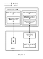
このコンテキストにおいて、メモリをクリアすることは、メモリ中に記憶されたデータが消去され、かつ/または上書きされることが許可されることを意味する。実際、クリアリングは、メモリユニット中のすべてのデータが上書きされてもよいように、メモリユニット向けのすべてのメモリアドレスを割振り解除することを伴う場合がある。他の例では、クリアリングは、どの以前記憶されたデータもそれ以上利用可能でないように、メモリユニット中のすべてのデータを(たとえば、すべて1またはすべて0で)上書きすることを伴う場合がある。メモリユニットがクリアされない場合、非セキュアジョブは、セキュアデータの末尾の残りを非セキュアメモリにコピーすることができる。この問題は、セキュアソフトウェア技法、ハードウェア技法、または両方の技法の組合せにより解決することができる。それにもかかわらず、クリアリングおよび非セキュアへの遷移は、この動作が非セキュアドライバによってトリガされるので、アトミック動作である場合がある。このコンテキストにおいて、アトミック動作は、非セキュアモードへの遷移と一緒に(すなわち、自動的に)内部GPU12メモリをクリアリングすることを含む。たとえば、両方を行う(モードを変え、内部メモリをクリアする)単一の「コマンド」がなければならず、そうでない場合、悪意のあるソフトウェアが、非セキュアモードへの遷移だけを実施し、クリアリング動作を実行しない可能性がある。
In this context, clearing the memory means that the data stored in the memory is allowed to be erased and / or overwritten. In fact, clearing may involve deallocating all memory addresses for the memory unit so that all data in the memory unit may be overwritten. In other examples, clearing may involve overwriting all data in a memory unit (eg, all 1s or all 0s) so that no more previously stored data is available . If the memory unit is not cleared, the non-secure job can copy the rest of the secure data to the non-secure memory. This problem can be solved by secure software techniques, hardware techniques, or a combination of both techniques. Nevertheless, clearing and transition to non-secure may be atomic operations because this operation is triggered by a non-secure driver. In this context, the atomic operation involves clearing the
いくつかの例では、セキュアモードから非セキュアモードに遷移するとき、GPU12のすべての記憶ユニットをクリアする必要がない場合がある。そうではなく、セキュアコンテンツへの無許可アクセスを効果的に防止するために、記憶ユニットの一部分のみがクリアされる必要がある。一例として、記憶されたコンテンツの半分だけがクリアされてもよい。別の例として、1つおきのデータチャンク(たとえば、1つおきの32バイトのデータ)がクリアされてもよい。
In some examples, when transitioning from secure mode to non-secure mode, it may not be necessary to clear all storage units of
図8は、本開示の一例によるキャッシュクリアリング技法を示すブロック図である。図8の例では、セキュアソフトウェアソリューションは、GPUをセキュアおよび非セキュアモードの間で遷移させるのに使用される。一例では、GPUレジスタ(たとえば、クリアレジスタ74)は、ホストCPU6上で稼動するセキュアソフトウェア(たとえば、セキュアOS54)の制御下にある。GPUドライバ7がGPU12のメモリモードを非セキュアモードからセキュアモードに切り替えた場合、GPUドライバ7は、L2キャッシュ61、GMEM70、および他のレジスタ72を含む、GPU12のキャッシュ、メモリまたはレジスタ上に残っているどのセキュアコンテンツもクリアするために、セキュアOS54中のセキュアソフトウェアも呼び出す。その時点で、セキュアOS54は、メモリクリアおよび/または無効化命令をクリアレジスタ74に書き込むことによって、GPU12上のジョブを最初に起動することもできる。そのような命令の結果、GPU12中の残っているセキュアデータすべてがクリアされることになる。そのような命令は、シェーダプログラム、メモリ書込みおよび/またはレジスタプログラミング(たとえば、GPU L2キャッシュ無効化)の組合せであってもよい。
FIG. 8 is a block diagram illustrating a cache clearing technique according to an example of the present disclosure. In the example of FIG. 8, the secure software solution is used to transition the GPU between secure and non-secure modes. In one example, the GPU register (eg, clear register 74) is under the control of secure software (eg, secure OS 54) running on the
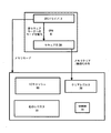
図9は、本開示の別の例によるキャッシュクリアリング技法を示すブロック図である。図9の例では、ハードウェアソリューションは、GPU12をセキュアおよび非セキュアモードの間で遷移させるのに使用される。この例では、外部的に可視的な(たとえば、メモリマップト入出力(MMIO))または内部(たとえば、コマンドストリーム)レジスタ76は、グラフィックスドライバ7によって直接書き込まれるように構成されてもよい。GPU12のハードウェアは、レジスタ76が書き込まれたとき(たとえば、セキュアモードから非セキュアモードに進んだとき)、GPU12のハードウェアが現在のセキュアジョブを完了し、パイプラインを流し(すなわち、処理されるどの残っているセキュアコンテンツも削除し)、クリアし、かつ/またはL2キャッシュ61、GMEM70、および他のレジスタ72を含むセキュアコンテンツを含むことができるすべてのレジスタ、メモリ、およびキャッシュを無効にするように構成されてもよい。このクリアリングプロセスは、GPU12上に常駐する、配線接続されるか、またはセキュアにロードされ、保護されたシェーダコードを使用することを含んでもよい。
FIG. 9 is a block diagram illustrating a cache clearing technique according to another example of the present disclosure. In the example of FIG. 9, the hardware solution is used to transition the
図10は、本開示の一例による方法を示すフローチャートである。メモリアクセスコントローラ53を含むGPU12、およびメモリコントローラ100は、図10の技法を実施するように構成されてもよい。
FIG. 10 is a flowchart illustrating a method according to an example of the present disclosure. The
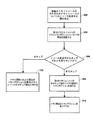
本開示の一例では、メモリアクセスコントローラ53は、GPU12の少なくとも1つのハードウェアユニットからのメモリトランザクションをメモリコントローラ100中の非セキュアコンテキストバンクに向けることによって、非セキュアモードに従って、メモリ(たとえば、システムメモリ10)の非セキュア部分にアクセスするように構成されてもよい(202)。メモリアクセスコントローラ53は、GPU12の少なくとも1つのハードウェアユニットからのメモリトランザクションをメモリコントローラ100中のセキュアコンテキストバンクに向けることによって、セキュアモードに従って、メモリのセキュア部分にアクセスするようにさらに構成されてもよい(204)。本開示の一例では、セキュアコンテキストバンクは、メモリの非セキュア部分への読取り専用ページテーブルエントリおよびメモリのセキュア部分への読取り/書込みページテーブルエントリを含み、非セキュアコンテキストバンクは、メモリの非セキュア部分への読取り専用ページテーブルエントリを含む。本開示の別の例では、メモリコントローラ100は、セキュアコンテキストバンクの読取り専用ページテーブルエントリ内に含まれるアドレスにデータを書き込むための要求が受信されると(206)、ページフォールトを発行する(208)ように構成されてもよい。
In one example of the present disclosure, the
本開示の別の例では、GPUの少なくとも1つのハードウェアユニットは、頂点フェッチ復号ユニット、高レベルシーケンサ、頂点シェーダ、ピクセルシェーダ、およびレンダバックエンドユニットのうちの1つまたは複数を含む。 In another example of the present disclosure, at least one hardware unit of the GPU includes one or more of a vertex fetch decoding unit, a high level sequencer, a vertex shader, a pixel shader, and a render backend unit.
本開示の別の例では、GPU12は、GPU12が非セキュアモードで動作しているか、またはセキュアモードで動作しているかにかかわらず、非セキュアコンテキストバンクを通して、フロントエンドコマンドプロセッサを用いて、メモリの非セキュア部分にアクセスするように構成されてもよい。
In another example of this disclosure, the
本開示の別の例では、GPUドライバ7は、GPU12をセキュアモードまたは非セキュアモードに置くように構成されてもよい。本開示のさらに別の例では、GPU12は、GPUドライバ7から、GPU12の1つまたは複数の内部メモリをクリアしかつ無効にするための、GPU12のコマンドストリームレジスタへの命令を受信するように構成されてもよい。GPU12は、GPU12がコマンドストリームレジスタ中の命令に基づいて、セキュアモードから非セキュアモードに遷移されると、少なくとも何らかのコンテンツを、GPU12の1つまたは複数の内部メモリからクリアしかつ無効にするようにさらに構成されてもよい。
In another example of the present disclosure, the
本開示の別の例では、GPU12は、クリアレジスタにおいて、GPUの1つまたは複数の内部メモリをクリアしかつ無効にするための指示を受信し、GPU12がクリアレジスタ中の指示に基づいて、セキュアモードから非セキュアモードに遷移されると、少なくとも何らかのコンテンツを、GPU12の1つまたは複数の内部メモリからクリアしかつ無効にするように構成されてもよい。
In another example of the present disclosure, the
図11は、本開示の一例による方法を示すフローチャートである。メモリアクセスコントローラ53を含むGPU12は、図11の技法を実施するように構成されてもよい。
FIG. 11 is a flowchart illustrating a method according to an example of the present disclosure. The
本開示の一例では、GPU12は、非セキュアモードおよびセキュアモードのうちの1つと、複数のメモリリソースの各々に関連付けられたそれぞれのリソース記述子とに従って、第1のメモリユニット(たとえば、システムメモリ10)にアクセスするように構成されてもよい。メモリアクセスコントローラ53は、複数のメモリリソースの各々に関連付けられたそれぞれのリソース記述子を読み取り(302)、第1のメモリユニットへのメモリトランザクションについての要求を受信する(304)ように構成されてもよい。
In an example of the present disclosure, the
メモリアクセスコントローラ53は、メモリトランザクションについての要求に関連したメモリリソースに関連付けられたリソース記述子が、セキュア記述子であるか、または非セキュアリソース記述子であるか判断する(306)ようにさらに構成されてもよい。メモリアクセスコントローラ53は、要求に応答して、GPU12がセキュアモードに従って動作しているとき、それぞれのリソース記述子がセキュアリソース記述子である複数のメモリリソースのうちのメモリリソースに関するメモリ読取りおよび書込みトランザクションを第1のメモリユニットのセキュア部分に向ける(312)ようにさらに構成されてもよい。メモリアクセスコントローラ53は、要求に応答して、GPU12がセキュアモードに従って動作しているとき、それぞれのリソース記述子が非セキュアリソース記述子である複数のメモリリソースのうちのメモリリソースに関するメモリ読取りトランザクションを第1のメモリユニットの非セキュア部分に向ける(308)ようにさらに構成されてもよい。メモリアクセスコントローラ53はまた、要求に応答して、GPU12がセキュアモードに従って動作しているとき、それぞれのリソース記述子が非セキュアリソース記述子である複数のメモリリソースのうちのメモリリソースに関するメモリ書込みトランザクションを取り下げる(310)ように構成されてもよい。
The
本開示の別の例では、メモリアクセスコントローラ53は、要求に応答して、GPU12が非セキュアモードに従って動作しているとき、それぞれのリソース記述子が非セキュアリソース記述子である複数のメモリリソースのうちのメモリリソースに関するメモリ読取りおよび書込みトランザクションを第1のメモリユニットの非セキュア部分に向け、要求に応答して、GPU12が非セキュアモードに従って動作しているとき、それぞれのリソース記述子がセキュアリソース記述子である複数のメモリリソースのうちのメモリリソースに関するメモリ読取りおよび書込みトランザクションを取り下げるようにさらに構成される。
In another example of the present disclosure, in response to a request, the
本開示の別の例では、メモリアクセスコントローラ53は、セキュアメモリ管理ユニットを使用することによって、第1のメモリユニットのセキュア部分にデータを書き込むように構成され、セキュアメモリ管理ユニットは、第1のメモリユニットのセキュア部分についてのアドレス範囲を含むセキュアページテーブルを使用する。本開示の別の例では、メモリアクセスコントローラ53は、非セキュアメモリ管理ユニットを使用することによって、第1のメモリユニットの非セキュア部分からデータを読み取るように構成され、非セキュアメモリ管理ユニットは、第1のメモリユニットの非セキュア部分についてのアドレス範囲を含む非セキュアページテーブルを使用する。
In another example of the present disclosure, the
本開示の別の例では、メモリアクセスコントローラ53は、仮想メモリアドレスの範囲からの仮想メモリアドレスに従って、データを読み取り、書き込むように構成され、仮想メモリアドレスの範囲は、セキュアメモリ管理ユニットによって使用されるセキュアページテーブル中のエントリに関する仮想メモリアドレスの第1の範囲、および非セキュアメモリ管理ユニットによって使用される非セキュアページテーブル中のエントリに関する仮想メモリアドレスの第2の範囲を含む。
In another example of the present disclosure, the
1つまたは複数の例では、上記で説明した機能は、ハードウェア、ソフトウェア、ファームウェア、またはそれらの任意の組合せで実装されてもよい。ソフトウェアで実装される場合、機能は、非一時的コンピュータ可読媒体を備える製造品上の1つまたは複数の命令またはコードとして記憶されてもよい。コンピュータ可読媒体は、コンピュータデータ記憶媒体を含んでもよい。データ記憶媒体は、本開示で説明した技法を実装するための命令、コード、および/またはデータ構造を取り出すために1つまたは複数のコンピュータまたは1つまたは複数のプロセッサによってアクセスすることのできる任意の利用可能な媒体であってもよい。限定ではなく例として、そのようなコンピュータ可読媒体は、RAM、ROM、EEPROM、CD-ROMもしくは他の光ディスクストレージ、磁気ディスクストレージもしくは他の磁気ストレージデバイス、フラッシュメモリ、または、命令もしくはデータ構造の形態の所望のプログラムコードを搬送もしくは記憶するために使用することができ、コンピュータによってアクセスすることができる、任意の他の媒体を備えることができる。本明細書で使用するディスク(disk)およびディスク(disc)は、コンパクトディスク(disc)(CD)、レーザーディスク(登録商標)(disc)、光ディスク(disc)、デジタル多用途ディスク(disc)(DVD)、フロッピーディスク(disk)、およびブルーレイディスク(disc)を含み、ディスク(disk)は、通常、データを磁気的に再生し、ディスク(disc)は、レーザーを用いてデータを光学的に再生する。上記の組合せもコンピュータ可読媒体の範囲に含まれるべきである。 In one or more examples, the functions described above may be implemented in hardware, software, firmware, or any combination thereof. If implemented in software, the functions may be stored as one or more instructions or code on an article of manufacture comprising a non-transitory computer readable medium. The computer readable medium may include a computer data storage medium. Any data storage medium may be accessed by one or more computers or one or more processors to retrieve instructions, code, and / or data structures for implementing the techniques described in this disclosure. It may be an available medium. By way of example, and not limitation, such computer readable media can be in the form of RAM, ROM, EEPROM, CD-ROM or other optical disk storage, magnetic disk storage or other magnetic storage device, flash memory, or instructions or data structures Any other medium that can be used to carry or store the desired program code and that can be accessed by a computer can be provided. The discs and discs used in this specification are compact discs (CD), laser discs (discs), optical discs (discs), digital versatile discs (DVDs) ), Floppy disk, and Blu-ray disc, the disk normally reproduces data magnetically, and the disc optically reproduces data using a laser . Combinations of the above should also be included within the scope of computer-readable media.
コードは、1つまたは複数のDSP、汎用マイクロプロセッサ、ASIC、FPGA、または他の等価の集積論理回路もしくはディスクリート論理回路などの、1つまたは複数のプロセッサによって実行されてもよい。加えて、いくつかの態様では、本明細書で説明する機能性は、専用のハードウェアモジュールおよび/またはソフトウェアモジュール内で提供されてもよい。また、本技法は、1つまたは複数の回路または論理要素において完全に実装することができる。 The code may be executed by one or more processors, such as one or more DSPs, general purpose microprocessors, ASICs, FPGAs, or other equivalent integrated or discrete logic circuits. In addition, in some aspects, the functionality described herein may be provided in dedicated hardware modules and / or software modules. The techniques can also be fully implemented in one or more circuits or logic elements.
本開示の技法は、ワイヤレスハンドセット、集積回路(IC)、またICのセット(たとえば、チップセット)を含む、様々なデバイスまたは装置において実装されてもよい。本開示では、開示される技法を実行するように構成されるデバイスの機能的側面を強調するために、様々な構成要素、モジュール、またはユニットが説明されているが、それらは、必ずしも異なるハードウェアユニットによる実現を必要とするとは限らない。むしろ、上記で説明したように、様々なユニットは、コーデックハードウェアユニットにおいて結合されてよく、または好適なソフトウェアおよび/もしくはファームウェアとともに、上記で説明したような1つもしくは複数のプロセッサを含む相互動作可能なハードウェアユニットの集合によって設けられてもよい。 The techniques of this disclosure may be implemented in a variety of devices or apparatuses, including wireless handsets, integrated circuits (ICs), and sets of ICs (eg, chipsets). Although this disclosure describes various components, modules, or units to emphasize functional aspects of a device configured to perform the disclosed techniques, they are not necessarily different hardware. It does not necessarily require realization by units. Rather, as described above, the various units may be combined in a codec hardware unit, or interoperate including one or more processors as described above, with suitable software and / or firmware. It may be provided by a set of possible hardware units.
様々な例について述べた。これらおよび他の例は、以下の特許請求の範囲内に入る。 Various examples have been described. These and other examples are within the scope of the following claims.
2 コンピューティングデバイス
4 ユーザ入力インターフェース
6 中央処理ユニット(CPU)
7 GPUドライバ、グラフィックスドライバ
8 メモリコントローラ
10 システムメモリ
11A メモリユニット
11N メモリユニット
12 グラフィックス処理ユニット(GPU)
14 グラフィックスメモリ
15 フレームバッファ
16 ディスプレイインターフェース
18 ディスプレイ
20 バス、システムバス
22 バス、メモリバス
24 ソフトウェアアプリケーション
26 グラフィックスAPI
30 グラフィックス処理パイプライン、グラフィックス3D処理パイプライン
32 コマンドエンジン
34 ジオメトリ処理ステージ
36 ラスタ化ステージ
38 ピクセル処理パイプライン
39 汎用シェーダ
40 IOMMU
42 仮想ページ
44 物理ページ
44A 部分
44B 部分
50 メモリコントローラ
51 非セキュアIOMMU
52 セキュアIOMMU
53 メモリアクセスコントローラ
54 セキュアオペレーティングシステム(OS)
56 非セキュアメモリ
57 セキュアメモリ
60 VBIF
61 L2キャッシュ
62 コマンドプロセッサ(CP)
65 頂点フェッチ復号(VFD)ユニット
66 高レベルシーケンサ(HLSQ)
67 頂点シェーダ(VS)
68 ピクセルシェーダ(PS)
69 レンダバックエンド(RB)
70 グラフィックスメモリ(GMEM)
71 GPUハードウェアブロック
72 他のレジスタ
73 クライアント
74 クリアレジスタ
76 レジスタ
100 メモリコントローラ
102 非セキュアコンテキストバンク
104 非セキュアPTエントリ
105 セキュアコンテキストバンク
106 非セキュアPTエントリ
108 セキュアPTエントリ
2 Computing devices
4 User input interface
6 Central processing unit (CPU)
7 GPU driver, graphics driver
8 Memory controller
10 System memory
11A memory unit
11N memory unit
12 Graphics processing unit (GPU)
14 Graphics memory
15 frame buffer
16 Display interface
18 display
20 bus, system bus
22 bus, memory bus
24 Software applications
26 Graphics API
30 Graphics processing pipeline, Graphics 3D processing pipeline
32 Command engine
34 Geometry processing stage
36 Rasterization stage
38 pixel processing pipeline
39 General purpose shader
40 IOMMU
42 virtual pages
44 Physical pages
44A part
44B part
50 Memory controller
51 Non-secure IOMMU
52 Secure IOMMU
53 Memory access controller
54 Secure Operating System (OS)
56 Non-secure memory
57 Secure memory
60 VBIF
61 L2 cache
62 Command processor (CP)
65 Vertex Fetch Decoding (VFD) unit
66 High-level sequencer (HLSQ)
67 Vertex Shader (VS)
68 pixel shader (PS)
69 Render Backend (RB)
70 Graphics memory (GMEM)
71 GPU hardware block
72 Other registers
73 clients
74 Clear register
76 registers
100 memory controller
102 Non-secure context bank
104 Non-secure PT entry
105 Secure Context Bank
106 Non-secure PT entry
108 Secure PT entry
Claims (30)
非セキュアモードおよびセキュアモードのうちの1つと、複数のメモリリソースの各々に関連付けられたそれぞれのリソース記述子とに従って、第1のメモリユニットにアクセスするように構成されるグラフィックス処理ユニット(GPU)を備え、前記GPUは、
前記複数のメモリリソースの各々に関連付けられた前記それぞれのリソース記述子を読み取るように構成されるメモリアクセスコントローラを備え、
前記メモリアクセスコントローラは、前記第1のメモリユニットへのメモリトランザクションについての要求を受信するように構成され、
前記メモリアクセスコントローラは、前記要求に応答して、前記GPUが前記セキュアモードに従って動作しているとき、前記それぞれのリソース記述子がセキュアリソース記述子である前記複数のメモリリソースのうちのメモリリソースに関するすべてのメモリ読取りおよび書込みトランザクションを前記第1のメモリユニットのセキュア部分に向けるように構成され、
前記メモリアクセスコントローラは、前記要求に応答して、前記GPUが前記セキュアモードに従って動作しているとき、前記それぞれのリソース記述子が非セキュアリソース記述子である前記複数のメモリリソースのうちのメモリリソースに関するすべてのメモリ読取りトランザクションを前記第1のメモリユニットの非セキュア部分に向けるように構成され、
前記メモリアクセスコントローラは、前記要求に応答して、前記GPUが前記セキュアモードに従って動作しているとき、前記それぞれのリソース記述子が前記非セキュアリソース記述子である前記複数のメモリリソースのうちのメモリリソースに関するすべてのメモリ書込みトランザクションを取り下げるように構成される、
装置。 A device for graphics processing,
A graphics processing unit (GPU) configured to access the first memory unit according to one of non-secure mode and secure mode and a respective resource descriptor associated with each of the plurality of memory resources The GPU is
A memory access controller configured to read the respective resource descriptor associated with each of the plurality of memory resources;
The memory access controller is configured to receive a request for a memory transaction to the first memory unit;
In response to the request, the memory access controller relates to a memory resource of the plurality of memory resources, wherein each resource descriptor is a secure resource descriptor when the GPU is operating according to the secure mode. Configured to direct all memory read and write transactions to a secure portion of the first memory unit;
The memory access controller, in response to the request, when the GPU is operating in accordance with the secure mode, the memory resource of the plurality of memory resources, each of which is a non-secure resource descriptor Configured to direct all memory read transactions with respect to the non-secure portion of the first memory unit;
The memory access controller, in response to the request, when the GPU is operating according to the secure mode, the memory resource of the plurality of memory resources, wherein the respective resource descriptor is the non-secure resource descriptor Configured to withdraw all memory write transactions for the resource,
apparatus.
前記メモリアクセスコントローラは、前記要求に応答して、前記GPUが前記非セキュアモードに従って動作しているとき、前記それぞれのリソース記述子が前記セキュアリソース記述子である前記複数のメモリリソースのうちのメモリリソースに関するメモリ読取りおよび書込みトランザクションを取り下げるようにさらに構成される、
請求項1に記載の装置。 The memory access controller, in response to the request, when the GPU is operating according to the non-secure mode, the respective resource descriptor is the non-secure resource descriptor of the plurality of memory resources Further configured to direct memory read and write transactions for memory resources to the non-secure portion of the first memory unit;
The memory access controller, in response to the request, when the GPU is operating according to the non-secure mode, the memory resource of the plurality of memory resources, wherein the respective resource descriptor is the secure resource descriptor Further configured to withdraw memory read and write transactions for the resource;
The apparatus according to claim 1.
前記メモリアクセスコントローラは、非セキュアメモリ管理ユニットを使用して前記第1のメモリユニットの前記非セキュア部分からデータを読み取るように構成され、前記非セキュアメモリ管理ユニットは、前記第1のメモリユニットの前記非セキュア部分についてのアドレス範囲を含む非セキュアページテーブルを使用する、
請求項1に記載の装置。 The memory access controller is configured to write data to the secure portion of the first memory unit using a secure memory management unit, the secure memory management unit comprising the secure portion of the first memory unit Use a secure page table containing address ranges for
The memory access controller is configured to read data from the non-secure portion of the first memory unit using a non-secure memory management unit, the non-secure memory management unit comprising: Using a non-secure page table that includes an address range for the non-secure portion;
The apparatus according to claim 1.
前記非セキュアメモリ管理ユニットと、
セキュアオペレーティングシステムおよび前記グラフィックスドライバを実行する中央処理ユニット(CPU)であって、前記セキュアオペレーティングシステムは、前記セキュアページテーブルを前記セキュアメモリ管理ユニットに、かつ前記非セキュアページテーブルを前記非セキュアメモリ管理ユニットに供給するように構成される中央処理ユニットと
をさらに備える、請求項5に記載の装置。 The secure memory management unit;
The non-secure memory management unit;
A central processing unit (CPU) for executing a secure operating system and the graphics driver, the secure operating system including the secure page table in the secure memory management unit and the non-secure page table in the non-secure memory 6. The apparatus of claim 5, further comprising: a central processing unit configured to supply to the management unit.
前記GPUが前記非セキュアモードにあるか、または前記セキュアモードにあるかにかかわらず、前記第1のメモリの前記非セキュア部分にデータを書き込むように構成される1つまたは複数のハードウェアブロックであって、前記1つまたは複数のハードウェアブロックは、前記第1のメモリユニットの前記セキュア部分への読取りアクセスを有さない、ハードウェアブロック
をさらに備える、請求項1に記載の装置。 The GPU is
One or more hardware blocks configured to write data to the non-secure portion of the first memory regardless of whether the GPU is in the non-secure mode or the secure mode. The apparatus of claim 1, wherein the one or more hardware blocks further comprises a hardware block that does not have read access to the secure portion of the first memory unit.
第1のメモリユニットへのメモリトランザクションについての要求を受信するステップと、
前記要求に応答して、グラフィックス処理ユニット(GPU)がセキュアモードに従って動作しているとき、前記それぞれのリソース記述子がセキュアリソース記述子である前記複数のメモリリソースのうちのメモリリソースに関するメモリ読取りおよび書込みトランザクションを前記第1のメモリユニットのセキュア部分に向けるステップと、
前記要求に応答して、前記GPUが前記セキュアモードに従って動作しているとき、前記それぞれのリソース記述子が非セキュアリソース記述子である前記複数のメモリリソースのうちのメモリリソースに関するメモリ読取りトランザクションを前記第1のメモリユニットの非セキュア部分に向けるステップと、
前記要求に応答して、前記GPUが前記セキュアモードに従って動作しているとき、前記それぞれのリソース記述子が前記非セキュアリソース記述子である前記複数のメモリリソースのうちのメモリリソースに関するメモリ書込みトランザクションを取り下げるステップと
を含む、方法。 Reading each resource descriptor for each memory resource of the plurality of memory resources;
Receiving a request for a memory transaction to a first memory unit;
In response to the request, when a graphics processing unit (GPU) is operating according to a secure mode, a memory read for a memory resource of the plurality of memory resources, wherein each resource descriptor is a secure resource descriptor Directing a write transaction to a secure portion of the first memory unit;
In response to the request, when the GPU is operating according to the secure mode, a memory read transaction for a memory resource of the plurality of memory resources, wherein the respective resource descriptor is a non-secure resource descriptor, Directing to the non-secure portion of the first memory unit;
In response to the request, when the GPU is operating according to the secure mode, a memory write transaction related to a memory resource of the plurality of memory resources, wherein the respective resource descriptor is the non-secure resource descriptor. A method comprising: withdrawing step.
前記要求に応答して、前記GPUが前記非セキュアモードに従って動作しているとき、前記それぞれのリソース記述子が前記セキュアリソース記述子である前記複数のメモリリソースのうちのメモリリソースに関するメモリ読取りおよび書込みトランザクションを取り下げるステップと
をさらに含む、請求項11に記載の方法。 In response to the request, when the GPU is operating according to the non-secure mode, a memory read for a memory resource of the plurality of memory resources, wherein the respective resource descriptor is the non-secure resource descriptor; and Directing a write transaction to a non-secure portion of the first memory unit;
In response to the request, when the GPU is operating in accordance with the non-secure mode, memory reads and writes for memory resources of the plurality of memory resources, wherein the respective resource descriptor is the secure resource descriptor The method of claim 11, further comprising: withdrawing the transaction.
非セキュアメモリ管理ユニットを使用して前記第1のメモリユニットの前記非セキュア部分からデータを読み取るステップであって、前記非セキュアメモリ管理ユニットは、前記第1のメモリユニットの前記非セキュア部分についてのアドレス範囲を含む非セキュアページテーブルを使用する、ステップと
をさらに含む、請求項11に記載の方法。 Writing data to the secure portion of the first memory unit using a secure memory management unit, the secure memory management unit including an address range for the secure portion of the first memory unit Use secure page table, steps,
Reading data from the non-secure portion of the first memory unit using a non-secure memory management unit, the non-secure memory management unit for the non-secure portion of the first memory unit The method of claim 11, further comprising: using a non-secure page table that includes an address range.
をさらに含む、請求項13に記載の方法。 Reading and writing data according to virtual memory addresses from a range of virtual memory addresses, wherein the range of virtual memory addresses is a virtual memory address of an entry in the secure page table used by the secure memory management unit The method of claim 13, further comprising: a first range and a second range of virtual memory addresses for entries in the non-secure page table used by the non-secure memory management unit.
をさらに含む、請求項15に記載の方法。 16. The method of claim 15, further comprising: supplying the secure page table to the secure memory management unit and the non-secure page table to the non-secure memory management unit.
前記命令に応答して、前記GPUが前記セキュアモードから前記非セキュアモードに遷移されると、少なくとも何らかのコンテンツを前記1つまたは複数の内部メモリからクリアかつ無効にするステップと
をさらに含む、請求項16に記載の方法。 Sending an instruction to the clear register of the GPU;
Further comprising clearing and invalidating at least some content from the one or more internal memories when the GPU is transitioned from the secure mode to the non-secure mode in response to the instructions. 16. The method according to 16.
前記命令に応答して、前記GPUが前記セキュアモードから前記非セキュアモードに遷移されると、少なくとも何らかのコンテンツを前記1つまたは複数の内部メモリからクリアかつ無効にするステップと
をさらに含む、請求項16に記載の方法。 Sending an instruction to the command stream register of the GPU;
Further comprising clearing and invalidating at least some content from the one or more internal memories when the GPU is transitioned from the secure mode to the non-secure mode in response to the instructions. 16. The method according to 16.
をさらに含む、請求項11に記載の方法。 Writing data from one or more hardware blocks of the GPU to the non-secure portion of the first memory regardless of whether the GPU is in the non-secure mode or the secure mode 12. The method of claim 11, further comprising: the one or more hardware blocks do not have read access to the secure portion of the first memory unit.
複数のメモリリソースのそれぞれのメモリリソースについてのそれぞれのリソース記述子を読み取るための手段と、
第1のメモリユニットへのメモリトランザクションについての要求を受信するための手段と、
前記要求に応答して、グラフィックス処理ユニット(GPU)がセキュアモードに従って動作しているとき、前記それぞれのリソース記述子がセキュアリソース記述子である前記複数のメモリリソースのうちのメモリリソースに関するメモリ読取りおよび書込みトランザクションを前記第1のメモリユニットのセキュア部分に向けるための手段と、
前記要求に応答して、前記GPUが前記セキュアモードに従って動作しているとき、前記それぞれのリソース記述子が非セキュアリソース記述子である前記複数のメモリリソースのうちのメモリリソースに関するメモリ読取りトランザクションを前記第1のメモリユニットの非セキュア部分に向けるための手段と、
前記要求に応答して、前記GPUが前記セキュアモードに従って動作しているとき、前記それぞれのリソース記述子が前記非セキュアリソース記述子である前記複数のメモリリソースのうちのメモリリソースに関するメモリ書込みトランザクションを取り下げるための手段と
を備える、装置。 A device for graphics processing,
Means for reading each resource descriptor for each memory resource of the plurality of memory resources;
Means for receiving a request for a memory transaction to a first memory unit;
In response to the request, when a graphics processing unit (GPU) is operating according to a secure mode, a memory read for a memory resource of the plurality of memory resources, wherein each resource descriptor is a secure resource descriptor And means for directing a write transaction to a secure portion of the first memory unit;
In response to the request, when the GPU is operating according to the secure mode, a memory read transaction for a memory resource of the plurality of memory resources, wherein the respective resource descriptor is a non-secure resource descriptor, Means for directing to the non-secure portion of the first memory unit;
In response to the request, when the GPU is operating according to the secure mode, a memory write transaction related to a memory resource of the plurality of memory resources, wherein the respective resource descriptor is the non-secure resource descriptor. Means for withdrawing.
前記要求に応答して、前記GPUが前記非セキュアモードに従って動作しているとき、前記それぞれのリソース記述子が前記セキュアリソース記述子である前記複数のメモリリソースのうちのメモリリソースに関するメモリ読取りおよび書込みトランザクションを取り下げるための手段と
をさらに備える、請求項21に記載の装置。 In response to the request, when the GPU is operating according to the non-secure mode, a memory read for a memory resource of the plurality of memory resources, wherein the respective resource descriptor is the non-secure resource descriptor; and Means for directing a write transaction to the non-secure portion of the first memory unit;
In response to the request, when the GPU is operating in accordance with the non-secure mode, memory reads and writes for memory resources of the plurality of memory resources, wherein the respective resource descriptor is the secure resource descriptor The apparatus of claim 21, further comprising: means for withdrawing the transaction.
非セキュアメモリ管理ユニットを使用して前記第1のメモリユニットの前記非セキュア部分からデータを読み取るための手段であって、前記非セキュアメモリ管理ユニットは、前記第1のメモリユニットの前記非セキュア部分についてのアドレス範囲を含む非セキュアページテーブルを使用する、手段と
をさらに備える、請求項21に記載の装置。 Means for writing data to the secure portion of the first memory unit using a secure memory management unit, the secure memory management unit including an address range for the secure portion of the first memory unit Means to use a secure page table containing
Means for reading data from the non-secure portion of the first memory unit using a non-secure memory management unit, the non-secure memory management unit comprising the non-secure portion of the first memory unit 23. The apparatus of claim 21, further comprising: means for using a non-secure page table that includes an address range for.
をさらに含む、請求項23に記載の装置。 Means for reading and writing data according to a virtual memory address from a range of virtual memory addresses, wherein the range of virtual memory addresses is a virtual memory associated with an entry in the secure page table used by the secure memory management unit 24. The apparatus of claim 23, further comprising means comprising: a first range of addresses and a second range of virtual memory addresses for entries in the non-secure page table used by the non-secure memory management unit. .
をさらに備える、請求項24に記載の装置。 25. The apparatus of claim 24, further comprising means for placing the GPU in a secure mode or a non-secure mode.
複数のメモリリソースのそれぞれのメモリリソースについてのそれぞれのリソース記述子を読み取ることと、
第1のメモリユニットへのメモリトランザクションについての要求を受信することと、
前記要求に応答して、グラフィックス処理ユニット(GPU)がセキュアモードに従って動作しているとき、前記それぞれのリソース記述子がセキュアリソース記述子である前記複数のメモリリソースのうちのメモリリソースに関するメモリ読取りおよび書込みトランザクションを前記第1のメモリユニットのセキュア部分に向けることと、
前記要求に応答して、前記GPUが前記セキュアモードに従って動作しているとき、前記それぞれのリソース記述子が非セキュアリソース記述子である前記複数のメモリリソースのうちのメモリリソースに関するメモリ読取りトランザクションを前記第1のメモリユニットの非セキュア部分に向けることと、
前記要求に応答して、前記GPUが前記セキュアモードに従って動作しているとき、前記それぞれのリソース記述子が前記非セキュアリソース記述子である前記複数のメモリリソースのうちのメモリリソースに関するメモリ書込みトランザクションを取り下げることと
を行わせる、コンピュータ可読記憶媒体。 A computer-readable storage medium storing instructions, wherein when executed, the instructions are executed by one or more processors,
Reading each resource descriptor for each memory resource of the plurality of memory resources;
Receiving a request for a memory transaction to a first memory unit;
In response to the request, when a graphics processing unit (GPU) is operating according to a secure mode, a memory read for a memory resource of the plurality of memory resources, wherein each resource descriptor is a secure resource descriptor Directing a write transaction to a secure portion of the first memory unit;
In response to the request, when the GPU is operating according to the secure mode, a memory read transaction for a memory resource of the plurality of memory resources, wherein the respective resource descriptor is a non-secure resource descriptor, Directing to the non-secure part of the first memory unit;
In response to the request, when the GPU is operating according to the secure mode, a memory write transaction related to a memory resource of the plurality of memory resources, wherein the respective resource descriptor is the non-secure resource descriptor. A computer-readable storage medium that allows the user to withdraw.
前記要求に応答して、前記GPUが前記非セキュアモードに従って動作しているとき、前記それぞれのリソース記述子が前記非セキュアリソース記述子である前記複数のメモリリソースのうちのメモリリソースに関するメモリ読取りおよび書込みトランザクションを、前記第1のメモリユニットの非セキュア部分に向けることと、
前記要求に応答して、前記GPUが前記非セキュアモードに従って動作しているとき、前記それぞれのリソース記述子が前記セキュアリソース記述子である前記複数のメモリリソースのうちのメモリリソースに関するメモリ読取りおよび書込みトランザクションを取り下げることと
をさらに行わせる、請求項26に記載のコンピュータ可読記憶媒体。 The instructions are sent to the one or more processors,
In response to the request, when the GPU is operating according to the non-secure mode, a memory read for a memory resource of the plurality of memory resources, wherein the respective resource descriptor is the non-secure resource descriptor; and Directing a write transaction to the non-secure portion of the first memory unit;
In response to the request, when the GPU is operating in accordance with the non-secure mode, memory reads and writes for memory resources of the plurality of memory resources, wherein the respective resource descriptor is the secure resource descriptor 27. The computer readable storage medium of claim 26, further causing withdrawing a transaction.
セキュアメモリ管理ユニットを使用して前記第1のメモリユニットの前記セキュア部分にデータを書き込むことであって、前記セキュアメモリ管理ユニットは、前記第1のメモリユニットの前記セキュア部分についてのアドレス範囲を含むセキュアページテーブルを使用する、書き込むことと、
非セキュアメモリ管理ユニットを使用して前記第1のメモリユニットの前記非セキュア部分からデータを読み取ることであって、前記非セキュアメモリ管理ユニットは、前記第1のメモリユニットの前記非セキュア部分についてのアドレス範囲を含む非セキュアページテーブルを使用する、読み取ることと
をさらに行わせる、請求項26に記載のコンピュータ可読記憶媒体。 The instructions are sent to the one or more processors,
Writing data to the secure portion of the first memory unit using a secure memory management unit, the secure memory management unit including an address range for the secure portion of the first memory unit Using a secure page table, writing,
Reading data from the non-secure portion of the first memory unit using a non-secure memory management unit, the non-secure memory management unit being configured for the non-secure portion of the first memory unit 27. The computer-readable storage medium of claim 26, further comprising: reading using a non-secure page table that includes an address range.
仮想メモリアドレスの範囲からの仮想メモリアドレスに従ってデータを読み取りかつ書き込むことであって、前記仮想メモリアドレスの範囲は、前記セキュアメモリ管理ユニットによって使用される前記セキュアページテーブル中のエントリに関する仮想メモリアドレスの第1の範囲、および前記非セキュアメモリ管理ユニットによって使用される前記非セキュアページテーブル中のエントリに関する仮想メモリアドレスの第2の範囲を含む、読み取りかつ書き込むこと
をさらに行わせる、請求項28に記載のコンピュータ可読記憶媒体。 The instructions are sent to the one or more processors,
Reading and writing data according to a virtual memory address from a range of virtual memory addresses, wherein the range of virtual memory addresses is a virtual memory address of an entry in the secure page table used by the secure memory management unit The read and write further comprising: a first range and a second range of virtual memory addresses for entries in the non-secure page table used by the non-secure memory management unit. Computer readable storage medium.
前記GPUをセキュアモードまたは非セキュアモードにさらに置かせる、請求項29に記載のコンピュータ可読記憶媒体。 The instructions are sent to the one or more processors,
30. The computer readable storage medium of claim 29, further causing the GPU to be placed in a secure mode or a non-secure mode.
Applications Claiming Priority (3)
| Application Number | Priority Date | Filing Date | Title |
|---|---|---|---|
| US14/821,174 US10102391B2 (en) | 2015-08-07 | 2015-08-07 | Hardware enforced content protection for graphics processing units |
| US14/821,174 | 2015-08-07 | ||
| PCT/US2016/043903 WO2017027196A1 (en) | 2015-08-07 | 2016-07-25 | Hardware enforced content protection for graphics processing units |
Publications (2)
| Publication Number | Publication Date |
|---|---|
| JP2018523876A true JP2018523876A (en) | 2018-08-23 |
| JP2018523876A5 JP2018523876A5 (en) | 2019-01-24 |
Family
ID=56609956
Family Applications (1)
| Application Number | Title | Priority Date | Filing Date |
|---|---|---|---|
| JP2018505701A Ceased JP2018523876A (en) | 2015-08-07 | 2016-07-25 | Hardware-enforced content protection for graphics processing units |
Country Status (7)
| Country | Link |
|---|---|
| US (1) | US10102391B2 (en) |
| EP (1) | EP3332346B1 (en) |
| JP (1) | JP2018523876A (en) |
| KR (1) | KR20180036970A (en) |
| CN (1) | CN107851138A (en) |
| BR (1) | BR112018002466A2 (en) |
| WO (1) | WO2017027196A1 (en) |
Families Citing this family (8)
| Publication number | Priority date | Publication date | Assignee | Title |
|---|---|---|---|---|
| FR3050847B1 (en) * | 2016-05-02 | 2019-04-05 | Morpho | METHOD OF OPTIMIZING MEMORY WRITINGS IN A DEVICE |
| US10380039B2 (en) * | 2017-04-07 | 2019-08-13 | Intel Corporation | Apparatus and method for memory management in a graphics processing environment |
| WO2020154924A1 (en) * | 2019-01-29 | 2020-08-06 | 华为技术有限公司 | Electronic device and address access method |
| EP3975018B1 (en) * | 2019-06-21 | 2024-08-07 | Huawei Technologies Co., Ltd. | Integrated chip and data processing method |
| CN110706147B (en) * | 2019-09-29 | 2023-08-11 | 阿波罗智联(北京)科技有限公司 | Image processing environment determination method, device, electronic equipment and storage medium |
| US11379135B2 (en) * | 2020-08-04 | 2022-07-05 | Honeywell International Inc. | Memory protection unit |
| CN113344764B (en) * | 2021-05-11 | 2024-04-19 | 中天恒星(上海)科技有限公司 | Secure graphics processor, processor chip, display card, apparatus, method, and storage medium |
| US20230153146A1 (en) * | 2021-11-12 | 2023-05-18 | Nvidia Corporation | Direct user mode work submission in secure computing enabled processors |
Citations (2)
| Publication number | Priority date | Publication date | Assignee | Title |
|---|---|---|---|---|
| WO2014126597A1 (en) * | 2013-02-18 | 2014-08-21 | Qualcomm Incorporated | Hardware enforced content protection for graphics processing units |
| US20150052325A1 (en) * | 2013-08-16 | 2015-02-19 | Arm Limited | Data processing systems |
Family Cites Families (53)
| Publication number | Priority date | Publication date | Assignee | Title |
|---|---|---|---|---|
| US4184201A (en) | 1978-04-26 | 1980-01-15 | Sperry Rand Corporation | Integrating processor element |
| US6986052B1 (en) | 2000-06-30 | 2006-01-10 | Intel Corporation | Method and apparatus for secure execution using a secure memory partition |
| US7055038B2 (en) | 2001-05-07 | 2006-05-30 | Ati International Srl | Method and apparatus for maintaining secure and nonsecure data in a shared memory system |
| US7065651B2 (en) | 2002-01-16 | 2006-06-20 | Microsoft Corporation | Secure video card methods and systems |
| JP4564756B2 (en) | 2002-04-18 | 2010-10-20 | アドバンスト・マイクロ・ディバイシズ・インコーポレイテッド | Method for initializing a computer system including a processor capable of operating in a secure execution mode |
| US7603550B2 (en) | 2002-04-18 | 2009-10-13 | Advanced Micro Devices, Inc. | Computer system including a secure execution mode-capable CPU and a security services processor connected via a secure communication path |
| KR20040000348A (en) | 2002-06-24 | 2004-01-03 | 마이크로소프트 코포레이션 | Systems and methods for securing video card output |
| GB0226906D0 (en) * | 2002-11-18 | 2002-12-24 | Advanced Risc Mach Ltd | Virtual to physical memory address mapping within a system having a secure domain and a non-secure domain |
| WO2004046924A1 (en) | 2002-11-18 | 2004-06-03 | Arm Limited | Processor switching between secure and non-secure modes |
| US7474312B1 (en) | 2002-11-25 | 2009-01-06 | Nvidia Corporation | Memory redirect primitive for a secure graphics processing unit |
| US7444523B2 (en) | 2004-08-27 | 2008-10-28 | Microsoft Corporation | System and method for using address bits to signal security attributes of data in the address space |
| US7502928B2 (en) * | 2004-11-12 | 2009-03-10 | Sony Computer Entertainment Inc. | Methods and apparatus for secure data processing and transmission |
| US7782329B2 (en) | 2004-12-10 | 2010-08-24 | Rockwell Collins, Inc. | Method and apparatus for protected graphics generation |
| US8473750B2 (en) | 2004-12-15 | 2013-06-25 | Nvidia Corporation | Chipset security offload engine |
| GB0427973D0 (en) | 2004-12-21 | 2005-01-26 | Falanx Microsystems As | Microprocessor systems |
| CN1984298B (en) | 2005-12-14 | 2010-05-19 | 辉达公司 | Chipset security offload engine |
| US7610464B2 (en) | 2006-02-22 | 2009-10-27 | Sony Computer Entertainment Inc. | Methods and apparatus for providing independent logical address space and access management |
| EP2030124A4 (en) | 2006-05-24 | 2012-12-12 | Safend Ltd | Method and system for defending security application in a user's computer |
| US20080077793A1 (en) | 2006-09-21 | 2008-03-27 | Sensory Networks, Inc. | Apparatus and method for high throughput network security systems |
| US7809934B2 (en) | 2006-10-13 | 2010-10-05 | Texas Instruments Incorporated | Security measures for preventing attacks that use test mechanisms |
| US7681077B1 (en) * | 2006-11-03 | 2010-03-16 | Nvidia Corporation | Graphics system with reduced shadowed state memory requirements |
| US20090079746A1 (en) | 2007-09-20 | 2009-03-26 | Apple Inc. | Switching between graphics sources to facilitate power management and/or security |
| US8478959B1 (en) | 2007-11-13 | 2013-07-02 | Nvidia Corporation | Method and system for protecting content in graphics memory |
| US20090150631A1 (en) | 2007-12-06 | 2009-06-11 | Clifton Labs, Inc. | Self-protecting storage device |
| US8156565B2 (en) | 2008-04-28 | 2012-04-10 | Microsoft Corporation | Hardware-based protection of secure data |
| US8393008B2 (en) | 2008-05-21 | 2013-03-05 | Microsoft Corporation | Hardware-based output protection of multiple video streams |
| US8578483B2 (en) | 2008-07-31 | 2013-11-05 | Carnegie Mellon University | Systems and methods for preventing unauthorized modification of an operating system |
| US8243088B2 (en) | 2009-02-26 | 2012-08-14 | Presagis | Two dimensional memory access controller |
| EP3001326B1 (en) | 2009-12-14 | 2017-07-26 | Citrix Systems Inc. | Methods and systems for communicating between trusted and non-trusted virtual machines |
| EP2515239B1 (en) | 2009-12-14 | 2017-03-29 | Panasonic Intellectual Property Management Co., Ltd. | Information processing apparatus |
| US20110202740A1 (en) * | 2010-02-17 | 2011-08-18 | Arm Limited | Storing secure page table data in secure and non-secure regions of memory |
| US8296538B2 (en) | 2010-02-17 | 2012-10-23 | Arm Limited | Storing secure mode page table data in secure and non-secure regions of memory |
| JP5485055B2 (en) | 2010-07-16 | 2014-05-07 | パナソニック株式会社 | Shared memory system and control method thereof |
| US20120036308A1 (en) * | 2010-08-06 | 2012-02-09 | Swanson Robert C | Supporting a secure readable memory region for pre-boot and secure mode operations |
| GB2482700A (en) | 2010-08-11 | 2012-02-15 | Advanced Risc Mach Ltd | Memory access control |
| US20120079270A1 (en) | 2010-09-29 | 2012-03-29 | Navin Patel | Hardware-Assisted Content Protection for Graphics Processor |
| CN101950262B (en) * | 2010-10-20 | 2011-09-28 | 深圳市开立科技有限公司 | Method and device for realizing safe mode in embedded system |
| GB2484717B (en) | 2010-10-21 | 2018-06-13 | Advanced Risc Mach Ltd | Security provision for a subject image displayed in a non-secure domain |
| CN103430185B (en) * | 2011-03-22 | 2016-10-26 | 瑞典爱立信有限公司 | For the method for switching between virtualization system operation and non-virtualized system operation |
| US8943330B2 (en) | 2011-05-10 | 2015-01-27 | Qualcomm Incorporated | Apparatus and method for hardware-based secure data processing using buffer memory address range rules |
| US9086989B2 (en) | 2011-07-01 | 2015-07-21 | Synopsys, Inc. | Extending processor MMU for shared address spaces |
| US8631212B2 (en) * | 2011-09-25 | 2014-01-14 | Advanced Micro Devices, Inc. | Input/output memory management unit with protection mode for preventing memory access by I/O devices |
| JP5664530B2 (en) | 2011-11-17 | 2015-02-04 | トヨタ自動車株式会社 | Operation check method of control device and memory protection device |
| US20130166922A1 (en) * | 2011-12-23 | 2013-06-27 | Ati Technologies Ulc | Method and system for frame buffer protection |
| GB2501274B (en) | 2012-04-17 | 2020-05-13 | Advanced Risc Mach Ltd | Management of data processing security in a secondary processor |
| US20130305388A1 (en) | 2012-05-10 | 2013-11-14 | Qualcomm Incorporated | Link status based content protection buffers |
| US9514064B2 (en) * | 2012-08-15 | 2016-12-06 | Synopsys, Inc. | Protection scheme for embedded code |
| US9633230B2 (en) | 2012-10-11 | 2017-04-25 | Intel Corporation | Hardware assist for privilege access violation checks |
| US9245129B2 (en) * | 2013-03-15 | 2016-01-26 | Nvidia Corporation | System and method for protecting data by returning a protect signal with the data |
| JP6067449B2 (en) | 2013-03-26 | 2017-01-25 | 株式会社東芝 | Information processing apparatus and information processing program |
| US9507961B2 (en) | 2013-07-01 | 2016-11-29 | Qualcomm Incorporated | System and method for providing secure access control to a graphics processing unit |
| US9483653B2 (en) | 2014-10-29 | 2016-11-01 | Square, Inc. | Secure display element |
| US9767320B2 (en) | 2015-08-07 | 2017-09-19 | Qualcomm Incorporated | Hardware enforced content protection for graphics processing units |
-
2015
- 2015-08-07 US US14/821,174 patent/US10102391B2/en active Active
-
2016
- 2016-07-25 JP JP2018505701A patent/JP2018523876A/en not_active Ceased
- 2016-07-25 CN CN201680042506.6A patent/CN107851138A/en active Pending
- 2016-07-25 EP EP16747953.4A patent/EP3332346B1/en active Active
- 2016-07-25 WO PCT/US2016/043903 patent/WO2017027196A1/en active Application Filing
- 2016-07-25 KR KR1020187003427A patent/KR20180036970A/en not_active Application Discontinuation
- 2016-07-25 BR BR112018002466A patent/BR112018002466A2/en not_active Application Discontinuation
Patent Citations (2)
| Publication number | Priority date | Publication date | Assignee | Title |
|---|---|---|---|---|
| WO2014126597A1 (en) * | 2013-02-18 | 2014-08-21 | Qualcomm Incorporated | Hardware enforced content protection for graphics processing units |
| US20150052325A1 (en) * | 2013-08-16 | 2015-02-19 | Arm Limited | Data processing systems |
Also Published As
| Publication number | Publication date |
|---|---|
| BR112018002466A2 (en) | 2018-09-18 |
| US20170039381A1 (en) | 2017-02-09 |
| EP3332346A1 (en) | 2018-06-13 |
| WO2017027196A1 (en) | 2017-02-16 |
| KR20180036970A (en) | 2018-04-10 |
| US10102391B2 (en) | 2018-10-16 |
| CN107851138A (en) | 2018-03-27 |
| EP3332346B1 (en) | 2021-02-24 |
Similar Documents
| Publication | Publication Date | Title |
|---|---|---|
| JP6385614B1 (en) | Hardware-enforced content protection for graphics processing units | |
| JP5917784B1 (en) | Hardware content protection for graphics processing units | |
| EP3332346B1 (en) | Hardware enforced content protection for graphics processing units | |
| US9134954B2 (en) | GPU memory buffer pre-fetch and pre-back signaling to avoid page-fault | |
| JP5844485B2 (en) | Techniques for reducing memory access bandwidth in graphics processing systems based on destination alpha value | |
| JP5866457B2 (en) | Switching between direct rendering and binning in graphic processing using an overdraw tracker | |
| CN105556487B (en) | The conditionity page error control that page is resident | |
| KR20190078086A (en) | A method and an apparatus for performing tile-based rendering using prefetched graphics data | |
| US9779471B2 (en) | Transparent pixel format converter | |
| US20240220425A1 (en) | Reserving a secure address range |
Legal Events
| Date | Code | Title | Description |
|---|---|---|---|
| A521 | Request for written amendment filed |
Free format text: JAPANESE INTERMEDIATE CODE: A523 Effective date: 20180208 |
|
| A521 | Request for written amendment filed |
Free format text: JAPANESE INTERMEDIATE CODE: A523 Effective date: 20181206 |
|
| A621 | Written request for application examination |
Free format text: JAPANESE INTERMEDIATE CODE: A621 Effective date: 20181206 |
|
| A871 | Explanation of circumstances concerning accelerated examination |
Free format text: JAPANESE INTERMEDIATE CODE: A871 Effective date: 20181206 |
|
| A975 | Report on accelerated examination |
Free format text: JAPANESE INTERMEDIATE CODE: A971005 Effective date: 20190221 |
|
| A01 | Written decision to grant a patent or to grant a registration (utility model) |
Free format text: JAPANESE INTERMEDIATE CODE: A01 Effective date: 20190304 |
|
| A045 | Written measure of dismissal of application [lapsed due to lack of payment] |
Free format text: JAPANESE INTERMEDIATE CODE: A045 Effective date: 20190729 |