JP2018509104A - Signal distribution / combining device in antenna device of mobile communication base station - Google Patents
Signal distribution / combining device in antenna device of mobile communication base station Download PDFInfo
- Publication number
- JP2018509104A JP2018509104A JP2017549038A JP2017549038A JP2018509104A JP 2018509104 A JP2018509104 A JP 2018509104A JP 2017549038 A JP2017549038 A JP 2017549038A JP 2017549038 A JP2017549038 A JP 2017549038A JP 2018509104 A JP2018509104 A JP 2018509104A
- Authority
- JP
- Japan
- Prior art keywords
- circuit board
- signal
- coupling
- signal distribution
- support plate
- Prior art date
- Legal status (The legal status is an assumption and is not a legal conclusion. Google has not performed a legal analysis and makes no representation as to the accuracy of the status listed.)
- Granted
Links
Images


Classifications
-
- H—ELECTRICITY
- H01—ELECTRIC ELEMENTS
- H01Q—ANTENNAS, i.e. RADIO AERIALS
- H01Q1/00—Details of, or arrangements associated with, antennas
- H01Q1/12—Supports; Mounting means
- H01Q1/22—Supports; Mounting means by structural association with other equipment or articles
- H01Q1/24—Supports; Mounting means by structural association with other equipment or articles with receiving set
- H01Q1/241—Supports; Mounting means by structural association with other equipment or articles with receiving set used in mobile communications, e.g. GSM
- H01Q1/246—Supports; Mounting means by structural association with other equipment or articles with receiving set used in mobile communications, e.g. GSM specially adapted for base stations
-
- H—ELECTRICITY
- H01—ELECTRIC ELEMENTS
- H01P—WAVEGUIDES; RESONATORS, LINES, OR OTHER DEVICES OF THE WAVEGUIDE TYPE
- H01P5/00—Coupling devices of the waveguide type
- H01P5/08—Coupling devices of the waveguide type for linking dissimilar lines or devices
- H01P5/085—Coaxial-line/strip-line transitions
-
- H—ELECTRICITY
- H01—ELECTRIC ELEMENTS
- H01P—WAVEGUIDES; RESONATORS, LINES, OR OTHER DEVICES OF THE WAVEGUIDE TYPE
- H01P5/00—Coupling devices of the waveguide type
- H01P5/12—Coupling devices having more than two ports
- H01P5/16—Conjugate devices, i.e. devices having at least one port decoupled from one other port
-
- H—ELECTRICITY
- H01—ELECTRIC ELEMENTS
- H01Q—ANTENNAS, i.e. RADIO AERIALS
- H01Q1/00—Details of, or arrangements associated with, antennas
- H01Q1/36—Structural form of radiating elements, e.g. cone, spiral, umbrella; Particular materials used therewith
- H01Q1/38—Structural form of radiating elements, e.g. cone, spiral, umbrella; Particular materials used therewith formed by a conductive layer on an insulating support
-
- H—ELECTRICITY
- H01—ELECTRIC ELEMENTS
- H01Q—ANTENNAS, i.e. RADIO AERIALS
- H01Q1/00—Details of, or arrangements associated with, antennas
- H01Q1/44—Details of, or arrangements associated with, antennas using equipment having another main function to serve additionally as an antenna, e.g. means for giving an antenna an aesthetic aspect
- H01Q1/46—Electric supply lines or communication lines
-
- H—ELECTRICITY
- H01—ELECTRIC ELEMENTS
- H01Q—ANTENNAS, i.e. RADIO AERIALS
- H01Q15/00—Devices for reflection, refraction, diffraction or polarisation of waves radiated from an antenna, e.g. quasi-optical devices
- H01Q15/14—Reflecting surfaces; Equivalent structures
-
- H—ELECTRICITY
- H01—ELECTRIC ELEMENTS
- H01R—ELECTRICALLY-CONDUCTIVE CONNECTIONS; STRUCTURAL ASSOCIATIONS OF A PLURALITY OF MUTUALLY-INSULATED ELECTRICAL CONNECTING ELEMENTS; COUPLING DEVICES; CURRENT COLLECTORS
- H01R9/00—Structural associations of a plurality of mutually-insulated electrical connecting elements, e.g. terminal strips or terminal blocks; Terminals or binding posts mounted upon a base or in a case; Bases therefor
- H01R9/03—Connectors arranged to contact a plurality of the conductors of a multiconductor cable, e.g. tapping connections
- H01R9/05—Connectors arranged to contact a plurality of the conductors of a multiconductor cable, e.g. tapping connections for coaxial cables
- H01R9/0515—Connection to a rigid planar substrate, e.g. printed circuit board
Abstract
移動通信基地局のアンテナ装置内の信号分配/結合装置において、上面に高周波信号分配/結合のための信号分配/結合用導体パターンが形成される回路基板と、回路基板と対応する大きさの上部実装面を有し、回路基板の下面が上部実装面に密着するかたちで、前記回路基板と結合して回路基板を支持し、下部はアンテナ装置の反射板と固定されるように結合する支持板を含み、支持板は、外部からの接続された信号伝達用ケーブルを支持及び固定する多数のケーブル支持を備える。【選択図】図2In a signal distribution / combining device in an antenna device of a mobile communication base station, a circuit board on which a signal distribution / coupling conductor pattern for high-frequency signal distribution / combination is formed on an upper surface, and an upper part corresponding to the circuit board A support plate having a mounting surface and supporting the circuit board by being coupled to the circuit board in such a manner that the lower surface of the circuit board is in close contact with the upper mounting surface, and the lower part being fixed to be fixed to the reflector of the antenna device The support plate includes a plurality of cable supports for supporting and fixing a signal transmission cable connected from the outside. [Selection] Figure 2
Description
本発明は、移動通信(PCS、Cellular、CDMA、GSM(登録商標)、LTEなど)のネットワークにおいて、基地局や中継局に適用することができるアンテナ装置に関し、特に、アンテナ装置内にて高周波(RF)信号を分配(または結合)するための信号分配/結合装置に関する。 The present invention relates to an antenna device that can be applied to a base station or a relay station in a network of mobile communication (PCS, Cellular, CDMA, GSM (registered trademark), LTE, etc.), and in particular, a high frequency ( RF) signal distribution / combining device for distributing (or combining) signals.
一般的に、移動通信システムの基地局や中継局(以下、「基地局」と称する)は、送受信信号処理のための基地局本体装置と、複数の放射素子を備えて無線信号を送受信するアンテナ装置とに区分してきた。通常、基地局本体装置は地上の低い位置に設置し、アンテナ装置は建物の屋上や塔などの高い位置に設置し、それを給電用ケーブル(feeding cable)などを介して接続する。 In general, a base station or a relay station (hereinafter referred to as “base station”) of a mobile communication system includes a base station main unit for transmission / reception signal processing and an antenna that includes a plurality of radiating elements to transmit and receive radio signals. It has been divided into devices. Usually, the base station main unit is installed at a low position on the ground, and the antenna device is installed at a high position on the roof of a building, a tower, etc., which are connected via a feeding cable or the like.
基地局のアンテナ装置は、高周波無線信号を送受信するための多数の放射素子を備える。このとき、放射素子は比較的広い面積の金属板状の反射板の一面(例えば、前面)に設置する。また、アンテナ装置は、前記多数の放射素子を介して送受信される信号処理のための様々な回路や装置が備えられ、例えば、前記反射板の背面に固定して設置する。これらの機器は、多数の放射素子の信号の位相を調整するための位相遷移器(phase shifter)と、内部の機器、そして放射素子の送受信信号の分配及び結合するための分配/結合装置などが備えられる。このとき、各機器は、信号伝達用伝送線路を介して接続し、これらの伝送線路の相当部分は同軸ケーブル(coaxial cable)を利用して構成する。 An antenna device of a base station includes a large number of radiating elements for transmitting and receiving high-frequency radio signals. At this time, the radiating element is installed on one surface (for example, the front surface) of a reflective plate having a relatively large area. The antenna device is provided with various circuits and devices for signal processing transmitted and received via the multiple radiating elements, and is fixedly installed on the back surface of the reflector, for example. These devices include a phase shifter for adjusting the phase of signals of a number of radiating elements, an internal device, and a distribution / combining device for distributing and combining signals transmitted and received by the radiating elements. Provided. At this time, each device is connected via a transmission line for signal transmission, and a substantial part of these transmission lines is configured using a coaxial cable.
一方、このような構造を有するアンテナ装置において、要求される帯域の信号の送受信特性を有することと共に、各機器そのものの構造や機器間の接続部における不連続な面または不安定な接続状態などによって発生するPIMD(Passive IntermodulatI/On DistortI/On)成分を抑制することが非常に重要な事項である。 On the other hand, the antenna device having such a structure has transmission / reception characteristics of a signal in a required band, and depending on a structure of each device itself, a discontinuous surface or an unstable connection state in a connection portion between devices, and the like. It is a very important matter to suppress the generated PIMD (Passive Intermodulat I / On Distort I / On) component.
このとき、アンテナ装置においては信号分配/結合装置と、これらの信号分配/結合装置と同軸ケーブルを用いてはんだ付け(soldering)を介して接続する構造は、ほぼ必然的に要求されることで、信号分配/結合装置と同軸ケーブルや機器との間の接続部で発生する接続状態の不安定や、はんだ付け状態の不均一などにより発生するPIMDを抑制するための効果的な方策が求められている。 At this time, in the antenna device, a signal distribution / combining device, and a structure for connecting these signal distribution / combining devices to the signal distribution / combining device through soldering using a coaxial cable are almost inevitably required. There is a need for an effective measure for suppressing PIMD that occurs due to instability in the connection state between the signal distribution / combining device and the coaxial cable or equipment, or uneven soldering. Yes.
従って、本発明の目的は、同軸ケーブルとの接続部において発生するPIMDを抑制することができ、前記接続部におけるはんだ付けの品質を安定化させ、装置の接地品質を安定化させるための移動通信基地局アンテナ装置内の信号分配/結合装置を提供することにある。 Therefore, an object of the present invention is to suppress the PIMD generated at the connection portion with the coaxial cable, to stabilize the soldering quality at the connection portion, and to stabilize the grounding quality of the apparatus. It is to provide a signal distribution / combining device in a base station antenna device.
前記の目的を達成するために、本発明は、移動通信基地局のアンテナ装置内の信号分配/結合装置において、上面に高周波信号分配/結合のための信号分配/結合用導体パターンが形成される回路基板と、前記回路基板と対応する大きさの上部実装面を有し、前記回路基板の下面が前記上部実装面に密着されるかたちで、前記回路基板と結合して前記回路基板を支持し、下部は前記アンテナ装置の反射板と固定されるように結合する支持板と、を含み、前記支持板は、外部からの接続された信号伝達用ケーブルを支持及び固定する多数のケーブル支持台を備え、前記多数のケーブル支持台は、前記信号分配/結合用導体パターンの多数の信号入出力部のうち、少なくとも一部に対応する部位に形成され、それぞれ前記ケーブルの外部導体が嵌合されるかたちで前記ケーブルを取り付けするために、前記ケーブルの外部導体に対応するかたちの構造物が長さ方向に延びるように形成された構造を有することを特徴とする。 In order to achieve the above object, according to the present invention, in a signal distribution / combining device in an antenna apparatus of a mobile communication base station, a signal distribution / combining conductor pattern for high-frequency signal distribution / combining is formed on an upper surface. A circuit board, and an upper mounting surface having a size corresponding to the circuit board, and the lower surface of the circuit board is in close contact with the upper mounting surface and is coupled to the circuit board to support the circuit board. A support plate coupled to be fixed to the reflector of the antenna device, and the support plate includes a plurality of cable support bases for supporting and fixing an externally connected signal transmission cable. The plurality of cable support bases are formed at portions corresponding to at least a part of the plurality of signal input / output portions of the signal distribution / coupling conductor pattern, and the outer conductors of the cables are respectively fitted thereinto. To mounting the cable in the form to be characterized as having a forming structure as a structure of the form corresponding to the outer conductor extend in the longitudinal direction of the cable.
前記多数のケーブル支持台は、前記ケーブルの内部導体が前記回路基板の上面と接する位置に載置されるように、前記支持板の予め設定された位置に形成される。 The plurality of cable support bases are formed at predetermined positions on the support plate so that the inner conductor of the cable is placed at a position in contact with the upper surface of the circuit board.
前記回路基板の下面と前記支持板にて、前記回路基板を実装する上部実装面は、互いにはんだ付け方法で接合されるためのはんだクリームが提供され、前記はんだクリームは、リフローはんだ付け方式で溶融及び硬化される。 A solder cream for bonding the circuit board on the lower surface of the circuit board and the support plate to each other by a soldering method is provided, and the solder cream is melted by a reflow soldering method. And cured.
前記回路基板の上面には、前記信号分配/結合用導体パターンと非接触カップリング方式によるカップリング信号を発生するためのカップリング導体パターンが形成される。 A coupling conductor pattern for generating a coupling signal by a non-contact coupling method is formed on the upper surface of the circuit board.
前記回路基板の上面には、前記信号分配/結合用導体パターン及び前記カップリング導体パターンと隣接した周辺領域に接地用導体パターンが形成され、前記接地用導体パターンは、多数のビアホールを介して前記回路基板の下面の接地層と電気的に接続する。 On the upper surface of the circuit board, a grounding conductor pattern is formed in a peripheral region adjacent to the signal distribution / coupling conductor pattern and the coupling conductor pattern, and the grounding conductor pattern is formed through the via holes. It is electrically connected to the ground layer on the lower surface of the circuit board.
前記支持板は、貫通領域が形成され、貫通領域を介して前記回路基板の下側から接続されるケーブルを装着するために、それぞれ前記ケーブルに対応するかたちの溝が形成された構造を有する多数のケーブルホルダーが形成される。 The support plate has a structure in which a through region is formed and grooves each having a shape corresponding to the cable are formed in order to mount a cable connected from the lower side of the circuit board through the through region. Cable holders are formed.
前記支持板には、前記アンテナ装置の反射板とネジ締結方式で固定されるように結合するためには、前記支持板の下側に突出し、ネジ締結溝が形成される多数の締結部材が形成される。 In order to be coupled to the support plate so as to be fixed to the reflection plate of the antenna device by a screw fastening method, a plurality of fastening members protruding below the support plate and having screw fastening grooves are formed. Is done.
前記支持板にて、前記回路基板を実装する実装面には、予め設定された長さ及び高さで突出する隔壁部材が一つ以上形成され、前記回路基板には、前記隔壁部材が挿入されるかたちで、前記隔壁部材と結合するスロットが一つ以上形成され、前記隔壁部材は、回路基板の導体パターンが形成された上面から予め設定された高さでさらに突出するように形成される。 In the support plate, one or more barrier rib members protruding at a predetermined length and height are formed on a mounting surface for mounting the circuit board, and the barrier rib member is inserted into the circuit board. One or more slots to be connected to the partition member are formed, and the partition member is further protruded at a predetermined height from the upper surface on which the conductor pattern of the circuit board is formed.
前記したように、本発明に係る移動通信基地局アンテナ装置内の信号分配/結合装置は、ケーブルとの接続部で発生するPIMDを抑制することができ、前記接続部においてはんだ付けの品質を安定化させることができ、また、装置の接地品質を安定化させることができる。 As described above, the signal distribution / combining device in the mobile communication base station antenna device according to the present invention can suppress the PIMD generated at the connection portion with the cable, and stabilize the soldering quality at the connection portion. In addition, the grounding quality of the apparatus can be stabilized.
以下、本発明に係る好適な実施例を添付した図面を参照して詳細に説明する。下の説明では、具体的な構成素子などの特定の事項を示すがこれは本発明のより全般的な理解を助けるために提供したに過ぎず、これらの特定の事項は本発明の範囲内で所定の変形や、あるいは変更が可能であることは、この技術分野で通常の知識を有する者には自明であろう。また、添付した図面では、同一の構成要素に対しては可能な限り同一の参照符号を付し、また、図面において却って過度に複雑に表示する余地がある参照符号に対する表記は省略した。 Hereinafter, preferred embodiments of the present invention will be described in detail with reference to the accompanying drawings. In the following description, specific items such as specific components are shown, but this is merely provided to aid a more general understanding of the present invention, and these specific items are within the scope of the present invention. It will be apparent to those skilled in the art that certain variations and modifications are possible. In the accompanying drawings, the same constituent elements are denoted by the same reference numerals as much as possible, and the reference numerals having room to be displayed in an excessively complicated manner in the drawings are omitted.
図1は、本発明の一実施形態に係る信号分配/結合装置が適用される移動通信基地局のアンテナ装置の概略的な構造図である。図1を参照すると、基地局のアンテナ装置は、全体的に比較的広い面積の金属板の形で構成され、その一面(例えば、前面)に無線信号を送受信するための多数の放射素子(図示せず)を装着する反射板1と、前記反射板1の他面(例えば、背面)において、例えば、上側及び下側にそれぞれ設置し、前記多数の放射素子に対する信号の位相を調整する上側及び下側位相遷移器6、5 と、前記反射板1と前記上側及び下側位相遷移器6、5 をはじめ、アンテナ内部の機器を全体的に包み込み、一体型な筒状に構成してなるレドーム4と、前記反射板1の上下部をそれぞれ固定し、前記筒状のレドーム4の上下の開放部を密封して結合する上部キャップ3及び下部キャップ2を含む。
FIG. 1 is a schematic structural diagram of an antenna apparatus of a mobile communication base station to which a signal distribution / combining apparatus according to an embodiment of the present invention is applied. Referring to FIG. 1, an antenna apparatus of a base station is generally formed in the form of a metal plate having a relatively large area, and a plurality of radiating elements (see FIG. 1) for transmitting and receiving a radio signal on one surface (for example, the front surface). (Not shown), and on the other surface (for example, the back surface) of the
また、前記アンテナ装置の前記反射板1の背面において、例えば、中央部には、本発明の一実施形態に係る信号分配/結合装置7が備えられる。信号分配/結合装置7は、例えば、アンテナ装置の外部の基地局本体装置(図示せず)側から入力される送信信号の提供を受け、前記上側及び下側位相遷移器6、5 をはじめとするアンテナ内部の機器に分配し、アンテナ装置の放射素子を介して受信した受信信号を結合し、基地局本体装置側へ出力する。
In addition, on the back surface of the
加えて、前記アンテナ装置のレドーム4内では、他の追加的な分配/結合回路や、またはアンプ、フィルタなどを備えることもでき、また、信号伝送の品質をはじめとするアンテナの様々な動作状態を検出するための検出回路や、全体的な動作を制御するため主制御装置(例えば、MCUなど)など、様々な電子部品(図示せず)が適切に設置する。ただし、図1では説明の便宜のために、このような電子部品の図示は省略した。 In addition, in the radome 4 of the antenna device, other additional distribution / combining circuits, amplifiers, filters, and the like can be provided, and various operating states of the antenna including signal transmission quality can be provided. Various electronic components (not shown), such as a detection circuit for detecting the error and a main controller (for example, MCU) for controlling the overall operation, are appropriately installed. However, in FIG. 1, illustration of such an electronic component is omitted for convenience of explanation.
一方、図1に示すように、通常、下部キャップ2には、送受信信号をアンテナ装置の内外に入出力するための多数の入出力コネクタ202が設置される。入出力コネクタ202は、複数の給電ケーブル8を介して基地局本体装置側と直接または間接的に接続する。アンテナ装置の内部では、前記下部キャップ2の入出力コネクタ202側と前記信号分配/結合装置7とは、信号伝達用伝送線路として多数の同軸ケーブル22を用いて接続する。また、信号分配/結合装置7と、上側及び下側位相遷移器6、5 もそれぞれ同軸ケーブル73、71を介して接続する。
On the other hand, as shown in FIG. 1, the
図1では、アンテナ装置の内部に上側及び下側位相遷移器6、5 が備えられることを例に挙げて説明しているが、他の構造のアンテナ装置では、例えば一つの位相遷移器だけを備えることもできる。そのような他の構造のアンテナ装置では、該当位相遷移器は反射板の背面の中央部に設置され、信号分配/結合装置は、反射板の背面から下側の部位に設置される。その場合には、該当信号分配/結合装置は、前記一つの位相遷移器及び放射素子をはじめとする他の機器に信号を分配するように構成することもできる。このように、多様な構造で具現するアンテナ装置に合わせ、信号分配/結合装置の設置位置、及び他の機器との接続構造を適切に設定する。
FIG. 1 illustrates an example in which the upper and
一方、信号分配/結合装置7は、高周波信号分配/結合のための導体パターンが形成されるプリント回路基板を主な構成として備える。通常、プリント回路基板に同軸ケーブルを接続する場合には、同軸ケーブルの内部導体をパターンの入出力端とはんだ付けする方式を適用する。同様に、前記信号分配/結合装置7に同軸ケーブルを接続する場合にも、はんだ付け方法で相互接続することになるが、この際、本発明の一実施形態に係る信号分配/結合装置7は、後述するように、特に、同軸ケーブルの接続部においてPIMDの発生を抑制することができる構造を提案する。 On the other hand, the signal distribution / combination device 7 mainly includes a printed circuit board on which a conductor pattern for high-frequency signal distribution / combination is formed. Usually, when a coaxial cable is connected to a printed circuit board, a method of soldering the inner conductor of the coaxial cable to the input / output end of the pattern is applied. Similarly, when a coaxial cable is connected to the signal distribution / combining device 7, the signal distribution / combining device 7 according to an embodiment of the present invention is interconnected by a soldering method. As will be described later, in particular, a structure capable of suppressing the occurrence of PIMD in the connection portion of the coaxial cable is proposed.
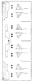
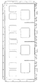
図2は、本発明の一実施形態に係る信号分配/結合装置7の斜視図であり、さらに反射板1を追加的に図示しており、図3は、図2の信号分配/結合装置7の回路基板74と支持板72の分離斜視図であり、図4及び図5は、それぞれ図2の信号分配/結合装置7の平面図及び背面図である。図6及び図7は、それぞれ図2の信号分配/結合装置7のうち、回路基板74の平面図及び背面図である。図8ないし図11は、それぞれ図2の信号分配/結合装置7のうち、支持板72の平面図、背面図、第1の側面側面、及び第2側面の側面であり、特に図10は、反射板1をさらに追加的に図示している。
FIG. 2 is a perspective view of a signal distribution / combining device 7 according to an embodiment of the present invention, and additionally shows a
図2ないし図11を参照すると、本発明の一実施形態に係る信号分配/結合装置7は、上面に少なくとも高周波信号分配/結合のための信号分配/結合用導体パターン742が形成される回路基板74と、前記回路基板74に対応する大きさの上部実装面を有し、前記回路基板74の下面が前記上部実装面に密着する形で前記回路基板74と結合して回路基板74を支持し、下部は前記アンテナ装置の反射板1と固定的に結合する、弾性のない硬い金属材料、例えば、アルミニウム(合金)製の支持板72を含んで構成される。
Referring to FIGS. 2 to 11, a signal distribution / combining device 7 according to an embodiment of the present invention is a circuit board having a signal distribution /
また、図2において、点線ボックスで表示したように、場合によっては、金属材料(例えば、アルミニウム合金)で構成されるキャップ形状のカバー76によって回路基板74の上側が覆われるように構成することもできる。カバー76は、支持板72とネジ結合によって固定するように構成する。このような構造は、支持板72及びカバー76が回路基板74を包み込む筐体の役割をする構造であることが分かる。このように、カバー76を備える場合には、回路基板74の信号処理機能がより安定になるが、該当信号分配/結合装置7の製品サイズが大きくなることから、該当アンテナ装置の設計に応じて前記カバー76の設置如何を適切に選択的に決定する。
In addition, as indicated by a dotted line box in FIG. 2, in some cases, the upper side of the
信号分配/結合装置7の回路基板74には、その上面に前記信号分配/結合用導体パターン742とともに、信号分配/結合用導体パターン742と非接触カップリング方式によるカップリング信号を発生するためのカップリング導体パターン743をさらに備えることができる。前記カップリング導体パターン743から発生したカップリング信号は、該当信号分配/結合用導体パターン742から伝送される信号の品質を確認するために関連機器に送信することができる。
On the upper surface of the
また、回路基板74の上面には、前記信号分配/結合用導体パターン742及びカップリング導体パターン743の接地特性を向上させるために、前記信号分配/結合用導体パターン742及び前記カップリング導体パターン743と隣接した周辺領域に接地用導体パターン745が追加で形成される。接地用導体パターン745において、特に端部の周りには、微細な直径の多数のビアホール(via hole)(図14の参照番号7452)が短い間隔で形成される。回路基板74の下面は、通常のプリント回路基板の構造と同様に、接地層が形成されるが、前記多数のビアホールは、回路基板74の上面の接地用導体パターン745と回路基板74の下面接地層を電気的に接続させることで、接地特性を満たす。
In addition, the signal distribution /
信号分配/結合装置7の支持板72は、前記回路基板74の下面と密着する形で、回路基板74と結合するが、本発明の特徴に応じて、回路基板74の下面と支持板72において回路基板74を実装する上部実装面は、互いにはんだ付け方法で接合する。例えば、回路基板74において支持板72に接合する部位にはんだクリーム(solder cream)を印刷し、はんだクリームが印刷された回路基板74を支持板72の実装面に実装した後、高熱炉(furnace)内でリフロー(reflow)はんだ付け方式ではんだクリームを溶融及び硬化させる。この時。支持板72の材質に応じて支持板72のはんだ付け作業が可能になるように、またははんだ付け品質を向上させるために、前記はんだクリームに対応する部位には、あらかじめスズなどのメッキ処理を施すこともある。このように、回路基板74と支持板72をリフローはんだ付け方式を用いて結合することで、回路基板74と支持板72の接地接触品質を大幅に安定化させることができる。
The
また、支持板72には、一部の領域が除去された貫通領域(図3のA領域で表示)を多数の部位に適切に形成することができる。支持板72に形成された貫通領域は、回路基板74が密着してはんだ付けする場合に空気通路を形成し、はんだ付け作業の効率を高めることになる。同様に、回路基板74の接地用導体パターン745に形成された多数のビアホールも回路基板74と支持板72のはんだ付け作業時に空気通路の役割をする。このように回路基板74の接地用導体パターン745には、接地特性を向上させるための用途に留まらず、前記のはんだ付け作業の効率を高めるための用途として多数のビアホールがさらに形成される。一方、前記支持板72に形成される貫通領域は、後述するように、他にも回路基板74の下側を通じて同軸ケーブルを接続しようとする場合にも活用される。
Further, the
また、支持板72には、信号伝達用の同軸ケーブルを支持及び固定する多数のケーブル支持台722を備える。多数のケーブル支持台722は、それぞれ同軸ケーブルの外部導体が嵌合されたり、または載置される形で前記同軸ケーブルを装着するために、同軸ケーブルの外部導体の形状と直径に対応する(一部の遊びを含む)形態及びサイズを有するかたち、例えば、U字状構造物が長さ方向に延びて形成された構造を有する。
The
前記支持板72上に装着される回路基板74において信号分配/結合用導体パターン742の多数の信号入出力部、すなわち、同軸ケーブルに接続される部位のうち、少なくとも一部は、回路基板74の一側端に形成されるように構成する。これにより、前記多数のケーブル支持台722は、前記信号分配/結合用導体パターン742の多数の信号入出力部に対応する部位に形成される。また、ケーブル支持台722によって固定される同軸ケーブルの内部導体が回路基板74の上面と離間せず、前記信号分配/結合用導体パターン742の信号入出力部に正確に合うように、前記ケーブル支持台722の形成部位が前記回路基板74の厚さなどを考慮して適切に設計される。
In the
前記ケーブル支持台722は、支持板72の一側から側面に突出するかたちで形成されるが、このような多数のケーブル支持台722を含む支持板72の全体構造は、例えば、ダイカスト工程を経て一体に形成する。
The
このような構成を有するケーブル支持台722に同軸ケーブルが装着されると、ケーブル支持台722と同軸ケーブルの外部導体の接触部位及び同軸ケーブルの内部導体と回路基板74の導体パターンとの接続部には、それぞれはんだ付け作業を行い、支持板72と同軸ケーブルが電気的および機構的に完全に固定されるように接続する。このようなケーブル支持台722を用いての信号伝達用の同軸ケーブルを支持板72に接続する方法は、作業の容易性と併せて正確かつ均一な処理が可能であり、作業後に該当製品の実際の使用環境においても支持板72と同軸ケーブルの接続状態が強固に維持される。したがって、当該信号分配/結合装置と同軸ケーブルとの接続部から発生するPIMDを大幅に抑制することができる。
When the coaxial cable is attached to the
一方、前記支持板72上に装着される回路基板74において信号分配/結合用導体パターン742および/またはカップリング導体パターン743の多数の信号入出力部のうちの一部は、回路基板74の下側を介して同軸ケーブルと接続するように形成することができる。その場合には、同軸ケーブルは、支持板72の下部から支持板72に形成された貫通領域を介して回路基板74と接続する。つまり、回路基板74に形成される導体パターンにおいて一部の信号入出力部をパターン設計に基づいて回路基板74の端部ではなく、内部に形成することもできる。その場合には、該当部位にケーブル接続用のホール(図5の参照番号748)を形成し、同軸ケーブルの内部導体は、該当ケーブル接続用ホールを介して回路基板74の下側から回路基板74の上側に突出するように挿入するかたちで設置する。
On the other hand, in the
前記支持板72においては、その下側に同軸ケーブルが回路基板74の下側から接続される同軸ケーブルを装着して支持および/または固定する多数のケーブルホルダー(holder)729をさらに備えることができる。前記多数のケーブルホルダー729は、それぞれ同軸ケーブルの被覆部分が嵌合されたり、または載置されるかたちで前記同軸ケーブルを装着するためには、少なくとも一部に同軸ケーブルの形状及び直径に対応する形態及びサイズを有する、例えば、U字状溝が支持板72の下面に形成された構造を有する。
The
また、図1及び図10により詳細に図示したように、支持板72の下部は、前記アンテナ装置の反射板1と固定されるように結合するが、そのために支持板72の下側に突出し、ネジ締結溝7242が形成される多数の締結部材724が支持板72の下部に形成される。多数の締結部材724は、例えば、長方形板状の支持板72の下部において各隅に対応する部位に、合計4つが形成され、支持板72が前記複数の締結部材724によって反射板1と接触するように、適切な高さで突出する。反射板1には、多数の締結部材724が接触する部位に対応する位置にそれぞれ多数のネジ挿入穴102が形成される。前記多数のネジ挿入穴102を貫通して前記締結部材724の多数のネジ締結溝7242に固定ネジ(図10の参照符号112)が締結されることで、支持板72が反射板1に固定されるように結合する。このような支持板72と反射板1の結合方式は、支持板72と反射板1との接触面積を最小限に抑え、締結部材724による接地接触の不安要素を最小限に抑えることができる。
Also, as shown in more detail in FIGS. 1 and 10, the lower portion of the
支持板72には、他にも回路基板74との結合作業を容易にし、結合状態を安定的に維持する機能などのために付加的な構造物が備えられる。例えば、支持板72には、回路基板74を実装する実装面の少なくとも一部を囲むかたちでガードレール部材725が形成される。また、支持板72において、前記回路基板74を実装する実装面には、結合用突起部材726が一つ以上形成され、これに対応するように回路基板74には、前記結合用突起部材726が挿入されるかたちで前記結合用突起部材726と結合する結合用ホール749が一つ以上形成される。また、支持板72においては、隔壁部材728が適切な長さで一つ以上形成され、これに対応するように回路基板74には、前記隔壁部材728が挿入されるかたちで、前記隔壁部材728と結合するスロット(slot)747が一つ以上形成される。
In addition, the
前記支持板72に形成される隔壁部材728は、支持板72と回路基板74との結合作業の容易性及び安定的な結合状態を維持するための機能だけでなく、回路基板74に形成された導体パターン間の信号漏れや信号の干渉を防止するための機能を有するように構成される。すなわち、前記隔壁部材728は、回路基板74の導体パターンが形成された上面において予め設定された高さにさらに突出するように形成される。これは隔壁部材728の両側において回路基板74上に形成された導体パターンとの間に、該当隔壁部材728によって電気的に接地状態の垂直壁が形成された構造を提供する。このような隔壁部材728により当該隔壁部材728をその間に置いた導体パターン間の信号漏れや信号の干渉を最小限に抑える。
The
例えば、アンテナ装置は、多重帯域のサービス構造を有することができ、前記信号/分配結合用導体パターン742は、各帯域毎に信号分配/結合のための導体パターンが区別して形成される。このような構造では、前記隔壁部材728は、帯域別に信号分配/結合のための導体パターンとの間に位置するように形成され、帯域毎の信号の漏れや信号の干渉を防止するように形成される。
For example, the antenna device may have a multi-band service structure, and the signal / distribution /
図12a及び図12bは、図2の信号分配/結合装置7と同軸ケーブル22との接続構造を示した一つの例示図であり、信号分配/結合装置7の上部においてケーブル支持台722に同軸ケーブル22が接続される状態が図示される。この時、図12a及び図12bは、信号分配/結合装置7と同軸ケーブル22が接続される前の状態と接続された後の状態をそれぞれ示す。図12a及び図12bに示すように、同軸ケーブル22は、接地導体である外部導体224及び信号伝達用の内部導体226がそれぞれ一定部分表れるように、絶縁及びケーブル保護のための被覆222及び外部導体224の一部が除去され、ケーブル支持台722に結合される。
FIGS. 12 a and 12 b are exemplary views showing a connection structure between the signal distribution / combining device 7 and the coaxial cable 22 of FIG. 2, and the coaxial cable is connected to the
このとき、ケーブル支持台722には、同軸ケーブル22の外部導体224が挿入されるかたちで嵌合されるようになり、ケーブル支持台722によって固定される同軸ケーブル22の内部導体226が、信号分配/結合用導体パターン742の信号入出力部と接することになる。以降、図12bから一点鎖線A部位で示すように、ケーブル支持台722と同軸ケーブル22の外部導体224の接触部位及び同軸ケーブル22の内部導体226と信号分配/結合用導体パターン742の接続部には、それぞれはんだ付け作業が行われる。
At this time, the
図13a、図13b及び図13cは、図2の信号分配/結合装置と同軸ケーブルとの接続構造を示した他の例示図であり、信号分配/結合装置7の下部においてケーブルホルダー729に同軸ケーブル22が接続される状態が図示されている。この時、図13aは、ケーブルホルダー729に同軸ケーブル71が接続された状態を示した平面図であり、図13b及び図13cは、図13aにおけるA−A '部分の切断面図であり、理解を助けるために、図13bには、同軸ケーブル22が除去された状態を示す。図13aないし図13cに示すように、同軸ケーブル71は、外部導体714及び内部導体716がそれぞれ一定部分表れるように、被覆712と外部導体714の一部が除去されてケーブルホルダー729に結合される。
FIGS. 13 a, 13 b and 13 c are other exemplary views showing a connection structure between the signal distribution / combining device of FIG. 2 and the coaxial cable, and the coaxial cable is connected to the
ケーブルホルダー729には、同軸ケーブル71の被覆712の部分が嵌合されたり載置される形で設置され、ケーブルホルダー729によって固定される同軸ケーブル71の外部導体714が回路基板74の下面の接地層と接することになる。同軸ケーブル71の内部導体716は、回路基板74に形成されたケーブル接続用ホール748に挿入される形で設置される。一方、ケーブルホルダー729には、同軸ケーブル71が嵌合された状態をより安定的に維持するために、該当同軸ケーブル71の側面を把持する構造でガード部材7292が形成される。
The
図14は、図2の信号分配/結合装置7のうち、回路基板74の一部の回路パターンの拡大図であり、例えば、図6に点線ボックスAの部分として表示した部分の回路パターンに該当する。また、当該回路パターンは、多重帯域サービス構造において一帯域の信号分配/結合するための回路構造に該当する。図14を参照し、回路基板74の信号分配/結合用導体パターン及びカップリング導体パターンの構造をより詳く説明する。
14 is an enlarged view of a part of the circuit pattern of the
まず、信号分配/結合用導体パターンを説明すると、例えば、第1の入出力コネクタ(I/Oコネクタ1)において同軸ケーブルを介して提供された信号(例えば、送信信号)は、第1の入力端(in1)であるa1パターンに入力され、a1パターンに入力された信号は、その後b1及びd1パターンで、下側位相遷移器(D/PS#1)、0度位相可変(つまり、位相可変なしの)放射素子1及び上側位相遷移器(U/PS#1)側に分配される。下側位相遷移器(D/PS#1)側に分配された信号は、c1パターンに提供され、放射素子1側に分配された信号は、e1のパターンに提供され、上側位相遷移器(U/PS#1)側に分配された信号は、f1パターンに提供される。
First, a signal distribution / coupling conductor pattern will be described. For example, a signal (for example, a transmission signal) provided via a coaxial cable in a first input / output connector (I / O connector 1) is a first input. The signal input to the a1 pattern, which is the end (in1), and the signal input to the a1 pattern is the b1 and d1 patterns, and then the lower phase shifter (D / PS # 1), 0 degree phase variable (that is, phase variable) Distributed to the
通常、アンテナ装置において、一のサービス帯域の放射素子は、垂直方向に一列に配置されるが、垂直ステアリング調整のために、通常垂直に配置された放射素子の位相を該当放射素子が配置された位置によって相対的に可変する。このような構造のアンテナにおいて、例えば、中央に位置する放射素子(位相可変なしの放射素子)を中心に上側に位置する放射素子は、前記上側位相遷移器を通じて[+]の角度でそれぞれ相互位相差を有するように位相可変し、下側に位置する放射素子は、前記下側位相遷移を介して、[―]の角度でそれぞれ相互位相差を有するように位相可変する。 Usually, in an antenna device, the radiating elements of one service band are arranged in a line in the vertical direction, but the radiating elements are arranged with the phase of the radiating elements arranged normally in the vertical direction for vertical steering adjustment. It is relatively variable depending on the position. In the antenna having such a structure, for example, the radiating element located on the upper side with respect to the radiating element located at the center (the radiating element having no phase variable) is mutually positioned at an angle of [+] through the upper phase shifter. The phase of the radiating element is varied so as to have a phase difference, and the phase of the radiating element located on the lower side is varied so as to have a mutual phase difference at an angle of [−] via the lower phase transition.
これに対応するように、前記のような信号分配/結合用導体パターンは、一入出力コネクタ(I/Oコネクタ1)から入力された信号を適切に分配してc1パターンを介して下側位相遷移器(D/PS# 1)側に伝達し、e1パターンを介しては、位相可変のない放射素子1側に伝達し、f1パターンを介しては、上側位相遷移器(U/PS#1)側に伝達する。前記a1ないしf1の各パターンの形状及び長さなどの詳細な構造は、分配および伝達する信号の位相及び相互インピーダンス等を考慮して適切に設計される。
[0065]
一方、第2の入出力コネクタ(I/Oコネクタ2)において同軸ケーブルを介して提供された信号は、第2の入力端(in2)であるa2パターンに入力され、以来、b2及びd2のパターンに分配され、以降c2パターン、f2パターン、およびe2パターンを介して下側位相遷移器(D/PS#2)、0度位相可変(つまり、位相可変なしの)放射素子2及び上側位相遷移器(U/PS#2)側に分配される。
Corresponding to this, the signal distribution / coupling conductor pattern as described above appropriately distributes the signal input from one input / output connector (I / O connector 1) and transmits the lower phase via the c1 pattern. Is transmitted to the transition unit (D / PS # 1) side, is transmitted to the
[0065]
On the other hand, the signal provided via the coaxial cable at the second input / output connector (I / O connector 2) is input to the a2 pattern which is the second input end (in2). Since then, the pattern of b2 and d2 The lower phase shifter (D / PS # 2), the 0 degree phase variable (ie, without phase variable) radiating
前記した信号分配/結合用導体パターンを見てみると、第1の入出力コネクタ(I/Oコネクタ1)にて入力された信号を処理するためのパターンは、例えば、二重偏波アンテナ構造において+45度偏波を発生する信号処理のパターンであり、第2の入出力コネクタ(I/Oコネクタ2)にて入力された信号を処理するためのパターンは、―45度偏波を発生する信号処理のパターンであることが分かる。また、前記した信号分配/結合用導体パターンは、送信信号を分配する機能を例に挙げて説明したが、該当パターンは送信動作の逆で、受信信号を結合してI/Oコネクタ側が提供する機能を実行できることが分かる。すなわち、図14に信号分配/結合用導体パターンは、アンテナ装置において2T2R(2Tx2Rx)の構造に対応する構造であり、図2等に示された全体の信号分配/結合用導体パターンは、全体的に8T8R構造に対応する構造である。 Looking at the signal distribution / coupling conductor pattern described above, a pattern for processing a signal input at the first input / output connector (I / O connector 1) is, for example, a dual polarization antenna structure. Is a pattern of signal processing that generates +45 degree polarization, and a pattern for processing a signal input at the second input / output connector (I / O connector 2) generates −45 degree polarization. It can be seen that this is a signal processing pattern. Further, the signal distribution / coupling conductor pattern described above has been described by taking the function of distributing a transmission signal as an example, but the corresponding pattern is the reverse of the transmission operation, and the received signal is coupled and provided by the I / O connector side. It can be seen that the function can be executed. That is, the signal distribution / coupling conductor pattern shown in FIG. 14 corresponds to the structure of 2T2R (2Tx2Rx) in the antenna device, and the entire signal distribution / coupling conductor pattern shown in FIG. The structure corresponds to the 8T8R structure.
一方、図14でカップリング導体パターンは、前記信号分配/結合導体パターンのうち、a1パターン及びa1パターンの伝達信号をそれぞれカップリングするためのh1パターン及びh2パターンを備える。 h1パターン及びh2パターンでカップリングされた信号は、その後i1パターンで結合されてj1パターンに伝達される。 j1パターンで伝達された信号は、その後、信号品質を確認するために関連機器(または外部)に伝達されるが、該当装置は、転送された信号を解析し、a1パターン及びa2パターンから送信される信号(例えば、送信信号)の品質を確認することができる。このとき、h1パターン及びh2パターンでカップリングされた信号がi1パターンで結合される構造であることから、信号の品質確認の際には、a1パターン及びa2パターンから送信される各送信信号の送信期間が互いに区別されるように設定する。 On the other hand, the coupling conductor pattern in FIG. 14 includes an h1 pattern and an h2 pattern for coupling transmission signals of the a1 pattern and the a1 pattern among the signal distribution / coupling conductor patterns. The signals coupled in the h1 pattern and the h2 pattern are then combined in the i1 pattern and transmitted to the j1 pattern. The signal transmitted in the j1 pattern is then transmitted to the related device (or outside) to confirm the signal quality, but the corresponding device analyzes the transferred signal and is transmitted from the a1 pattern and the a2 pattern. The quality of a signal (for example, a transmission signal) can be confirmed. At this time, since the signals coupled by the h1 pattern and the h2 pattern are combined by the i1 pattern, the transmission of each transmission signal transmitted from the a1 pattern and the a2 pattern is performed when the signal quality is confirmed. The period is set so as to be distinguished from each other.
図15は、本発明の他の実施形態に係る信号分配/結合装置の斜視図であり、図16及び図17は、それぞれ図15の信号分配/結合装置の平面図及び背面図である。図15ないし図17を参照すると、本発明の他の実施形態に係る信号分配/結合装置7は、前記図2等に示された一実施形態に係る構造と同様、上面に高周波信号分配/結合のための信号分配/結合用導体パターン842が形成される回路基板84と、前記回路基板84に対応する大きさの上部実装面を有し、前記回路基板84の下面が前記上部実装面に密着するかたちで、前記回路基板84と結合して回路基板84を支持し、下部は前記アンテナ装置の反射板と固定して結合される、支持板82を含んで構成される。ただし、図15ないし図17に図示された本発明の他の実施の構造は、前記図2等に示された一実施形態の構造に比べて回路基板74には、カップリング導体パターン(図2の743)や接地用導体パターン(図2の745)が形成されていない構造であることが分かる。
15 is a perspective view of a signal distribution / combining device according to another embodiment of the present invention, and FIGS. 16 and 17 are a plan view and a rear view of the signal distribution / combining device of FIG. 15, respectively. Referring to FIGS. 15 to 17, a signal distribution / combining device 7 according to another embodiment of the present invention has a high-frequency signal distribution / combination on the upper surface, similar to the structure according to the embodiment shown in FIG. A
加えて、前記の他の実施例の構造では、前記図2等に示された一実施形態の構造と同様に、支持板82には、信号伝達用の同軸ケーブルを支持および固定する多数のケーブル支持台822と、反射板と固定して結合するための多数の締結部材824及び、一部の領域が除去された貫通領域などが形成される。
In addition, in the structure of the other example, like the structure of the embodiment shown in FIG. 2 and the like, the
前記のように、本発明の実施例に係る移動通信基地局のアンテナ装置内の信号分配/結合装置の構成と動作が行われ、一方で、前記した本発明の説明では、具体的な実施形態について説明したが、様々な変形が、本発明の範囲を逸脱することなく実施することができる。 As described above, the configuration and operation of the signal distribution / combining device in the antenna device of the mobile communication base station according to the embodiment of the present invention is performed, while the above description of the present invention describes a specific embodiment. However, various modifications can be made without departing from the scope of the invention.
例えば、前記の説明では、本発明の実施例に係る信号分配/結合装置が、該当アンテナ装置の反射板の中央部において、入出力コネクタ、上側及び下側位相遷移器などと同軸ケーブルを介して接続されることを説明したが、加えて、信号分配/結合装置は、他の機器と同軸ケーブルを介して接続することができ、その設置位置も反射板の中央部位に加えて、他の部位に適切に設置する。 For example, in the above description, the signal distribution / combining device according to the embodiment of the present invention is connected to the input / output connector, the upper and lower phase shifters, and the like via the coaxial cable at the central portion of the reflector of the antenna device. In addition to the above description, the signal distribution / combining device can be connected to other devices via a coaxial cable, and the installation position of the signal distribution / combining device is not limited to the central portion of the reflector. Install properly.
また、前記の説明では、本発明の実施例に係る信号分配/結合装置の信号分配/結合用導体パターンは、全体的に8T8R構造に対応することを例に挙げて説明したが、他にも本発明は4T4R構造や他の構造に適用することができる。 In the above description, the signal distribution / combining conductor pattern of the signal distribution / combining apparatus according to the embodiment of the present invention is described as an example corresponding to the 8T8R structure as a whole. The present invention can be applied to 4T4R structures and other structures.
加えて、前記した実施形態では、回路基板の回路パターンの詳細構造や支持板の詳細構造などにおいて、様々な変形及び変更があり、したがって、本発明の範囲は、説明された実施例によって定めることがなく、請求の範囲と請求の範囲相当のものによって定めなければならならない。 In addition, in the above-described embodiment, there are various modifications and changes in the detailed structure of the circuit pattern of the circuit board, the detailed structure of the support plate, etc. Therefore, the scope of the present invention is defined by the described embodiments. And must be defined by the claims and their equivalents.
Claims (12)
上面に高周波信号分配/結合のための信号分配/結合用導体パターンが形成される回路基板と、
前記回路基板と対応する大きさの上部実装面を有し、前記回路基板の下面が前記上部実装面に密着されるかたちで、前記回路基板と結合して前記回路基板を支持し、下部は前記アンテナ装置の反射板と固定されるように結合する支持板と、を含み、
前記支持板は、外部からの接続された信号伝達用ケーブルを支持及び固定する多数のケーブル支持台を備え、前記多数のケーブル支持台は、前記信号分配/結合用導体パターンの多数の信号入出力部のうち、少なくとも一部に対応する部位に形成され、それぞれ前記ケーブルの外部導体が嵌合されるかたちで前記ケーブルを取り付けするために、前記ケーブルの外部導体に対応するかたちの構造物が長さ方向に延びるように形成された構造を有することを特徴とする信号分配/結合装置。 In a signal distribution / combining device in an antenna device of a mobile communication base station,
A circuit board having a signal distribution / coupling conductor pattern for high-frequency signal distribution / coupling formed on an upper surface;
An upper mounting surface of a size corresponding to the circuit board is provided, and the lower surface of the circuit board is bonded to the upper mounting surface to support the circuit board in combination with the circuit board, and the lower part is the A support plate coupled to be fixed to the reflector of the antenna device,
The support plate includes a plurality of cable support bases for supporting and fixing a signal transmission cable connected from the outside, and the plurality of cable support bases are a plurality of signal input / output terminals of the signal distribution / coupling conductor pattern. In order to attach the cable in such a manner that the outer conductor of the cable is fitted to the cable, the structure corresponding to the outer conductor of the cable is long. A signal distribution / combining device having a structure formed to extend in a vertical direction.
Applications Claiming Priority (3)
| Application Number | Priority Date | Filing Date | Title |
|---|---|---|---|
| KR10-2015-0035802 | 2015-03-16 | ||
| KR1020150035802A KR102324528B1 (en) | 2015-03-16 | 2015-03-16 | Device for dividing and coupling signal in antenna apparatus of mobile communication base transceiver station |
| PCT/KR2015/013737 WO2016148378A1 (en) | 2015-03-16 | 2015-12-15 | Signal distributing/combining apparatus in antenna apparatus of mobile communication base station |
Publications (2)
| Publication Number | Publication Date |
|---|---|
| JP2018509104A true JP2018509104A (en) | 2018-03-29 |
| JP6557732B2 JP6557732B2 (en) | 2019-08-07 |
Family
ID=56919102
Family Applications (1)
| Application Number | Title | Priority Date | Filing Date |
|---|---|---|---|
| JP2017549038A Active JP6557732B2 (en) | 2015-03-16 | 2015-12-15 | Signal distribution / combining device in antenna device of mobile communication base station |
Country Status (6)
| Country | Link |
|---|---|
| US (1) | US10249940B2 (en) |
| EP (1) | EP3273537B1 (en) |
| JP (1) | JP6557732B2 (en) |
| KR (1) | KR102324528B1 (en) |
| CN (1) | CN108377661B (en) |
| WO (1) | WO2016148378A1 (en) |
Families Citing this family (5)
| Publication number | Priority date | Publication date | Assignee | Title |
|---|---|---|---|---|
| KR102548871B1 (en) * | 2016-11-30 | 2023-06-28 | 주식회사 케이엠더블유 | Method for Cancelling Passive Inter-Modulation Distortion And Antenna Unit |
| CN109687100B (en) * | 2017-10-18 | 2020-11-06 | 康普技术有限责任公司 | Base station antenna assembly with feed panel having reduced passive intermodulation distortion |
| JP7178307B2 (en) * | 2019-03-22 | 2022-11-25 | 古河電気工業株式会社 | Electronic device, radar device and housing |
| CN213460078U (en) * | 2020-12-21 | 2021-06-15 | 康普技术有限责任公司 | Base station antenna and board assembly for base station antenna |
| US11707020B1 (en) | 2022-01-26 | 2023-07-25 | Arland Morrison | Cotton bale strapping apparatus and methods of use |
Citations (6)
| Publication number | Priority date | Publication date | Assignee | Title |
|---|---|---|---|---|
| DE3640937A1 (en) * | 1986-11-29 | 1988-06-01 | Licentia Gmbh | Microwave power divider |
| JPH04171997A (en) * | 1990-11-06 | 1992-06-19 | Fujitsu Ltd | Shielded connecting structure of coaxial cable |
| US5771025A (en) * | 1996-07-02 | 1998-06-23 | Omnipoint Corporation | Folded mono-bow antennas and antenna systems for use in cellular and other wireless communication systems |
| EP0973231A2 (en) * | 1998-07-06 | 2000-01-19 | Ace Technology | Dual polarization directional antenna having choke reflectors for minimizing side lobe |
| JP2006101467A (en) * | 2004-09-01 | 2006-04-13 | Alps Electric Co Ltd | Antenna assembly |
| KR20120068560A (en) * | 2010-12-17 | 2012-06-27 | 한국생산기술연구원 | Soldering method for magnesium alloy using plating and magnesium alloy phase shifter for mobile phone antenna using the same |
Family Cites Families (13)
| Publication number | Priority date | Publication date | Assignee | Title |
|---|---|---|---|---|
| US5018982A (en) * | 1990-07-25 | 1991-05-28 | Ncr Corporation | Adapter for stacking printed circuit boards |
| KR101017670B1 (en) * | 2007-10-05 | 2011-02-25 | 주식회사 에이스테크놀로지 | Antenna having a choke member |
| KR101188771B1 (en) * | 2008-07-04 | 2012-10-10 | 무라다기카이가부시끼가이샤 | Traveling vehicle system |
| CN101656350B (en) * | 2008-08-20 | 2013-01-09 | 华硕电脑股份有限公司 | Panel antenna and wireless communication device |
| CN102208710B (en) * | 2010-03-31 | 2014-11-19 | 安德鲁公司 | Structure for coupling grounding conversion from radio frequency coaxial cable to air microstrip and corresponding antenna |
| JP2012156993A (en) * | 2010-12-30 | 2012-08-16 | Telekom Malaysia Berhad | Folded dipole antenna with 450 mhz |
| KR101150168B1 (en) * | 2011-01-06 | 2012-05-25 | 주식회사 에이스테크놀로지 | Signal cable connection apparatus |
| KR101092628B1 (en) * | 2011-04-06 | 2011-12-13 | 주식회사 굿텔 | Cable fixed device, board installing the same, and antenna structure including the same |
| KR101279873B1 (en) * | 2011-04-08 | 2013-07-01 | (주)하이게인안테나 | Power divider |
| KR101305246B1 (en) * | 2011-10-25 | 2013-09-06 | 주식회사 감마누 | A phase shifter having a ground-hole |
| CN202423563U (en) * | 2012-01-09 | 2012-09-05 | 华为技术有限公司 | Antenna feed network and antenna |
| CN104882659B (en) * | 2015-05-26 | 2017-11-28 | 摩比通讯技术(吉安)有限公司 | Chamber power divider and antenna |
| DE102016108867A1 (en) * | 2016-05-13 | 2017-11-16 | Kathrein Werke Kg | Shield housing for HF applications |
-
2015
- 2015-03-16 KR KR1020150035802A patent/KR102324528B1/en active IP Right Grant
- 2015-12-15 EP EP15885679.9A patent/EP3273537B1/en active Active
- 2015-12-15 JP JP2017549038A patent/JP6557732B2/en active Active
- 2015-12-15 WO PCT/KR2015/013737 patent/WO2016148378A1/en active Application Filing
- 2015-12-15 CN CN201580077956.4A patent/CN108377661B/en active Active
-
2017
- 2017-09-15 US US15/705,294 patent/US10249940B2/en active Active
Patent Citations (6)
| Publication number | Priority date | Publication date | Assignee | Title |
|---|---|---|---|---|
| DE3640937A1 (en) * | 1986-11-29 | 1988-06-01 | Licentia Gmbh | Microwave power divider |
| JPH04171997A (en) * | 1990-11-06 | 1992-06-19 | Fujitsu Ltd | Shielded connecting structure of coaxial cable |
| US5771025A (en) * | 1996-07-02 | 1998-06-23 | Omnipoint Corporation | Folded mono-bow antennas and antenna systems for use in cellular and other wireless communication systems |
| EP0973231A2 (en) * | 1998-07-06 | 2000-01-19 | Ace Technology | Dual polarization directional antenna having choke reflectors for minimizing side lobe |
| JP2006101467A (en) * | 2004-09-01 | 2006-04-13 | Alps Electric Co Ltd | Antenna assembly |
| KR20120068560A (en) * | 2010-12-17 | 2012-06-27 | 한국생산기술연구원 | Soldering method for magnesium alloy using plating and magnesium alloy phase shifter for mobile phone antenna using the same |
Also Published As
| Publication number | Publication date |
|---|---|
| KR102324528B1 (en) | 2021-11-11 |
| EP3273537A1 (en) | 2018-01-24 |
| EP3273537B1 (en) | 2020-12-02 |
| CN108377661B (en) | 2020-05-05 |
| CN108377661A (en) | 2018-08-07 |
| US20180006363A1 (en) | 2018-01-04 |
| WO2016148378A1 (en) | 2016-09-22 |
| JP6557732B2 (en) | 2019-08-07 |
| KR20160111098A (en) | 2016-09-26 |
| EP3273537A4 (en) | 2018-12-05 |
| US10249940B2 (en) | 2019-04-02 |
Similar Documents
| Publication | Publication Date | Title |
|---|---|---|
| JP6557732B2 (en) | Signal distribution / combining device in antenna device of mobile communication base station | |
| CN107210541B (en) | Mobile base station antenna | |
| US9214733B2 (en) | Antenna device | |
| US8130164B2 (en) | Broadband coplanar antenna element | |
| WO2013044843A1 (en) | Antenna unit, antenna device, and antenna installation method | |
| JPH11355033A (en) | Antenna device | |
| US10461439B2 (en) | Flexible polymer antenna with multiple ground resonators | |
| US10797408B1 (en) | Antenna structure and method for manufacturing the same | |
| WO2020155723A1 (en) | Phase shift feed apparatus and base station antenna | |
| WO2016008607A1 (en) | Antenna arrangement and connector for an antenna arrangement | |
| KR20210120888A (en) | Radio-frequency arrangement having a frontside and a backside antenna | |
| KR101798628B1 (en) | Array Antenna for a base station | |
| WO2021103762A1 (en) | Antenna having integrated filter | |
| KR20120082279A (en) | Antenna including a radiator without plating | |
| EP3297092B1 (en) | Cable and high-frequency device using same | |
| CN109417213B (en) | Circuit board assembly for supplying signals to a transmitter | |
| KR20130044250A (en) | Antenna including a radiator without plating | |
| CN111063998A (en) | Antenna and feed calibration network device | |
| KR102529334B1 (en) | MIMO antenna and MIMO antenna apparatus having the same | |
| CN210957005U (en) | Antenna and feed calibration network device | |
| KR200334062Y1 (en) | Dipole antenna using dielectric board | |
| KR20160116662A (en) | Antenna device and mobile terminal with the same | |
| KR101333383B1 (en) | Antenna including a radiator without plating | |
| CN116325353A (en) | Antenna assembly and method of manufacturing the same | |
| US20150061959A1 (en) | Antenna device |
Legal Events
| Date | Code | Title | Description |
|---|---|---|---|
| A621 | Written request for application examination |
Free format text: JAPANESE INTERMEDIATE CODE: A621 Effective date: 20170915 |
|
| A131 | Notification of reasons for refusal |
Free format text: JAPANESE INTERMEDIATE CODE: A131 Effective date: 20181127 |
|
| A601 | Written request for extension of time |
Free format text: JAPANESE INTERMEDIATE CODE: A601 Effective date: 20190225 |
|
| A521 | Request for written amendment filed |
Free format text: JAPANESE INTERMEDIATE CODE: A523 Effective date: 20190315 |
|
| TRDD | Decision of grant or rejection written | ||
| A01 | Written decision to grant a patent or to grant a registration (utility model) |
Free format text: JAPANESE INTERMEDIATE CODE: A01 Effective date: 20190625 |
|
| A61 | First payment of annual fees (during grant procedure) |
Free format text: JAPANESE INTERMEDIATE CODE: A61 Effective date: 20190712 |
|
| R150 | Certificate of patent or registration of utility model |
Ref document number: 6557732 Country of ref document: JP Free format text: JAPANESE INTERMEDIATE CODE: R150 |
|
| R250 | Receipt of annual fees |
Free format text: JAPANESE INTERMEDIATE CODE: R250 |
|
| R250 | Receipt of annual fees |
Free format text: JAPANESE INTERMEDIATE CODE: R250 |