JP2018504032A - Gain control in complementary common gate and common source amplifiers. - Google Patents
Gain control in complementary common gate and common source amplifiers. Download PDFInfo
- Publication number
- JP2018504032A JP2018504032A JP2017532861A JP2017532861A JP2018504032A JP 2018504032 A JP2018504032 A JP 2018504032A JP 2017532861 A JP2017532861 A JP 2017532861A JP 2017532861 A JP2017532861 A JP 2017532861A JP 2018504032 A JP2018504032 A JP 2018504032A
- Authority
- JP
- Japan
- Prior art keywords
- signal
- gain
- current
- transistor
- shunt
- Prior art date
- Legal status (The legal status is an assumption and is not a legal conclusion. Google has not performed a legal analysis and makes no representation as to the accuracy of the status listed.)
- Pending
Links
Images


Classifications
-
- H—ELECTRICITY
- H03—ELECTRONIC CIRCUITRY
- H03F—AMPLIFIERS
- H03F1/00—Details of amplifiers with only discharge tubes, only semiconductor devices or only unspecified devices as amplifying elements
- H03F1/02—Modifications of amplifiers to raise the efficiency, e.g. gliding Class A stages, use of an auxiliary oscillation
- H03F1/0205—Modifications of amplifiers to raise the efficiency, e.g. gliding Class A stages, use of an auxiliary oscillation in transistor amplifiers
- H03F1/0261—Modifications of amplifiers to raise the efficiency, e.g. gliding Class A stages, use of an auxiliary oscillation in transistor amplifiers with control of the polarisation voltage or current, e.g. gliding Class A
- H03F1/0272—Modifications of amplifiers to raise the efficiency, e.g. gliding Class A stages, use of an auxiliary oscillation in transistor amplifiers with control of the polarisation voltage or current, e.g. gliding Class A by using a signal derived from the output signal
-
- H—ELECTRICITY
- H03—ELECTRONIC CIRCUITRY
- H03G—CONTROL OF AMPLIFICATION
- H03G3/00—Gain control in amplifiers or frequency changers without distortion of the input signal
- H03G3/20—Automatic control
- H03G3/30—Automatic control in amplifiers having semiconductor devices
- H03G3/3036—Automatic control in amplifiers having semiconductor devices in high-frequency amplifiers or in frequency-changers
-
- H—ELECTRICITY
- H03—ELECTRONIC CIRCUITRY
- H03F—AMPLIFIERS
- H03F1/00—Details of amplifiers with only discharge tubes, only semiconductor devices or only unspecified devices as amplifying elements
- H03F1/02—Modifications of amplifiers to raise the efficiency, e.g. gliding Class A stages, use of an auxiliary oscillation
- H03F1/0205—Modifications of amplifiers to raise the efficiency, e.g. gliding Class A stages, use of an auxiliary oscillation in transistor amplifiers
- H03F1/0277—Selecting one or more amplifiers from a plurality of amplifiers
-
- H—ELECTRICITY
- H03—ELECTRONIC CIRCUITRY
- H03F—AMPLIFIERS
- H03F3/00—Amplifiers with only discharge tubes or only semiconductor devices as amplifying elements
- H03F3/189—High frequency amplifiers, e.g. radio frequency amplifiers
- H03F3/19—High frequency amplifiers, e.g. radio frequency amplifiers with semiconductor devices only
- H03F3/193—High frequency amplifiers, e.g. radio frequency amplifiers with semiconductor devices only with field-effect devices
-
- H—ELECTRICITY
- H03—ELECTRONIC CIRCUITRY
- H03F—AMPLIFIERS
- H03F3/00—Amplifiers with only discharge tubes or only semiconductor devices as amplifying elements
- H03F3/26—Push-pull amplifiers; Phase-splitters therefor
- H03F3/265—Push-pull amplifiers; Phase-splitters therefor with field-effect transistors only
-
- H—ELECTRICITY
- H03—ELECTRONIC CIRCUITRY
- H03F—AMPLIFIERS
- H03F3/00—Amplifiers with only discharge tubes or only semiconductor devices as amplifying elements
- H03F3/45—Differential amplifiers
- H03F3/45071—Differential amplifiers with semiconductor devices only
- H03F3/45479—Differential amplifiers with semiconductor devices only characterised by the way of common mode signal rejection
- H03F3/45632—Differential amplifiers with semiconductor devices only characterised by the way of common mode signal rejection in differential amplifiers with FET transistors as the active amplifying circuit
- H03F3/45636—Differential amplifiers with semiconductor devices only characterised by the way of common mode signal rejection in differential amplifiers with FET transistors as the active amplifying circuit by using feedback means
- H03F3/45641—Measuring at the loading circuit of the differential amplifier
- H03F3/45654—Controlling the active amplifying circuit of the differential amplifier
-
- H—ELECTRICITY
- H03—ELECTRONIC CIRCUITRY
- H03G—CONTROL OF AMPLIFICATION
- H03G1/00—Details of arrangements for controlling amplification
- H03G1/0005—Circuits characterised by the type of controlling devices operated by a controlling current or voltage signal
- H03G1/0017—Circuits characterised by the type of controlling devices operated by a controlling current or voltage signal the device being at least one of the amplifying solid state elements of the amplifier
- H03G1/0029—Circuits characterised by the type of controlling devices operated by a controlling current or voltage signal the device being at least one of the amplifying solid state elements of the amplifier using FETs
-
- H—ELECTRICITY
- H03—ELECTRONIC CIRCUITRY
- H03G—CONTROL OF AMPLIFICATION
- H03G1/00—Details of arrangements for controlling amplification
- H03G1/0005—Circuits characterised by the type of controlling devices operated by a controlling current or voltage signal
- H03G1/0088—Circuits characterised by the type of controlling devices operated by a controlling current or voltage signal using discontinuously variable devices, e.g. switch-operated
-
- H—ELECTRICITY
- H03—ELECTRONIC CIRCUITRY
- H03G—CONTROL OF AMPLIFICATION
- H03G3/00—Gain control in amplifiers or frequency changers without distortion of the input signal
- H03G3/20—Automatic control
- H03G3/30—Automatic control in amplifiers having semiconductor devices
- H03G3/3052—Automatic control in amplifiers having semiconductor devices in bandpass amplifiers (H.F. or I.F.) or in frequency-changers used in a (super)heterodyne receiver
-
- H—ELECTRICITY
- H03—ELECTRONIC CIRCUITRY
- H03F—AMPLIFIERS
- H03F2200/00—Indexing scheme relating to amplifiers
- H03F2200/451—Indexing scheme relating to amplifiers the amplifier being a radio frequency amplifier
-
- H—ELECTRICITY
- H03—ELECTRONIC CIRCUITRY
- H03F—AMPLIFIERS
- H03F2200/00—Indexing scheme relating to amplifiers
- H03F2200/54—Two or more capacitor coupled amplifier stages in cascade
-
- H—ELECTRICITY
- H03—ELECTRONIC CIRCUITRY
- H03F—AMPLIFIERS
- H03F2200/00—Indexing scheme relating to amplifiers
- H03F2200/72—Indexing scheme relating to amplifiers the amplifier stage being a common gate configuration MOSFET
-
- H—ELECTRICITY
- H03—ELECTRONIC CIRCUITRY
- H03F—AMPLIFIERS
- H03F2200/00—Indexing scheme relating to amplifiers
- H03F2200/75—Indexing scheme relating to amplifiers the amplifier stage being a common source configuration MOSFET
-
- H—ELECTRICITY
- H03—ELECTRONIC CIRCUITRY
- H03F—AMPLIFIERS
- H03F2203/00—Indexing scheme relating to amplifiers with only discharge tubes or only semiconductor devices as amplifying elements covered by H03F3/00
- H03F2203/45—Indexing scheme relating to differential amplifiers
- H03F2203/45228—A transformer being added at the output or the load circuit of the dif amp
-
- H—ELECTRICITY
- H03—ELECTRONIC CIRCUITRY
- H03F—AMPLIFIERS
- H03F2203/00—Indexing scheme relating to amplifiers with only discharge tubes or only semiconductor devices as amplifying elements covered by H03F3/00
- H03F2203/45—Indexing scheme relating to differential amplifiers
- H03F2203/45731—Indexing scheme relating to differential amplifiers the LC comprising a transformer
Abstract
相補的共通ゲートおよび共通ソース増幅器おける利得制御が開示されている。例示的な実施形態において、装置は、第1の増幅された信号を生成するために、入力端子における入力信号を増幅するように構成された第1の増幅段を含む。第1の増幅段は、第1の増幅段の利得を設定するために、選択的に電流を分流する電流分流器を含む。装置はまた、第2の増幅された信号を生成するために、入力端子における入力信号を増幅するように構成された第2の増幅段を含む。第2の増幅段は、第2の増幅段の利得を設定するための、利得制御回路を含む。【選択図】図7Gain control in complementary common gate and common source amplifiers is disclosed. In an exemplary embodiment, the apparatus includes a first amplification stage configured to amplify an input signal at the input terminal to generate a first amplified signal. The first amplifier stage includes a current shunt that selectively shunts current to set the gain of the first amplifier stage. The apparatus also includes a second amplification stage configured to amplify the input signal at the input terminal to generate a second amplified signal. The second amplification stage includes a gain control circuit for setting the gain of the second amplification stage. [Selection] Figure 7
Description
[0001] 本開示は、一般的に、増幅器に関し、より具体的には、低ノイズ増幅器における利得制御に関する。 [0001] The present disclosure relates generally to amplifiers, and more specifically to gain control in low noise amplifiers.
[0002] ワイヤレス通信システムにおけるワイヤレスデバイス(たとえば、セルラー電話またはスマートフォン)は、双方向通信のために、データを送信および受信し得る。例えば、ワイヤレスデバイスは、周波数分割複信(FDD)システムにおいて、または時分割複信システム(TDD)において動作し得る。ワイヤレスデバイスは、データ送信のための送信機、およびデータ受信のための受信機を含み得る。よって、ワイヤレスデバイスは、通信および/またはデータサービスを提供するために、アナログおよびデジタル信号の両方を処理し得る。 [0002] A wireless device (eg, a cellular phone or a smartphone) in a wireless communication system may transmit and receive data for two-way communication. For example, a wireless device may operate in a frequency division duplex (FDD) system or in a time division duplex system (TDD). A wireless device may include a transmitter for data transmission and a receiver for data reception. Thus, a wireless device may process both analog and digital signals to provide communication and / or data services.
[0003] ワイヤレスデバイスにおける受信機は、RF信号を受信し、受信したRF信号を復調するために使用される。典型的な受信機は、復調の前に、受信したRF信号を増幅するための低ノイズ増幅器(LNA)を含む。インピーダンスマッチング、アイソレーション、および線形性は、受信機中のLNAについての主要な懸念である。例えば、受信アンテナのインピーダンスにマッチングするために、LNAが、典型的に50オームの入力インピーダンスを提供することが望ましい。復調の前に、受信したRF信号に適用される増幅が、正確に制御できるように、LNAはまた、正確な利得制御を提供すべきである。 [0003] A receiver in a wireless device is used to receive an RF signal and demodulate the received RF signal. A typical receiver includes a low noise amplifier (LNA) for amplifying the received RF signal prior to demodulation. Impedance matching, isolation, and linearity are major concerns for LNAs in the receiver. For example, in order to match the impedance of the receiving antenna, it is desirable for the LNA to provide an input impedance of typically 50 ohms. The LNA should also provide accurate gain control so that the amplification applied to the received RF signal can be accurately controlled prior to demodulation.
[0004] 残念ながら、従来のLNAは、所望の入力インピーダンスを提供するために、いくつかの外部コンポーネントを利用するであろう。これは、LNAにより必要とされる回路面積を増加する。また、従来のLNAにおける利得への調整は、入力インピーダンスに影響を及ぼし得るので、正確な利得制御は問題であろう。 [0004] Unfortunately, conventional LNAs will utilize several external components to provide the desired input impedance. This increases the circuit area required by the LNA. Also, adjustment to gain in a conventional LNA can affect the input impedance, so accurate gain control may be a problem.
[0005] それゆえ、従来の回路の不利を克服する、一定入力インピーダンスを伴う利得制御を有する、低電力増幅器を持つことが望ましい。 [0005] It is therefore desirable to have a low power amplifier with gain control with constant input impedance that overcomes the disadvantages of conventional circuits.
[0019] 下記で説明される詳細な説明は、本開示の例示的な設計の説明を意図しており、本開示が実践され得る唯一の設計を表示することを意図したものではない。「例示的な」という用語は、本明細書で「例、実例、または例証を提供する」という意味で使用される。「例示的な」と本明細書において説明された任意の設計は、他の設計よりも好適または利点があると必ずしも解釈されるべきではない。詳しい説明は、本開示の例示的な設計の完璧な理解を提供する目的で、特定の詳細を含む。本明細書において説明される、例示的な設計が、これらの特定の詳細なしに実施され得ることが、当業者にとって明らかとなるであろう。いくつかの事例において、良く知られている構造およびデバイスは、本明細書において提示されている例示的な設計の新規性を曖昧にすることを避けるために、ブロック図形式で指し示される。 [0019] The detailed description set forth below is intended as a description of exemplary designs of the present disclosure and is not intended to represent the only designs in which the present disclosure may be practiced. The term “exemplary” is used herein to mean “providing an example, instance, or illustration”. Any design described herein as "exemplary" is not necessarily to be construed as preferred or advantageous over other designs. The detailed description includes specific details for the purpose of providing a thorough understanding of the example designs of this disclosure. It will be apparent to those skilled in the art that the exemplary designs described herein can be practiced without these specific details. In some instances, well-known structures and devices are indicated in block diagram form in order to avoid obscuring the novelty of the exemplary designs presented herein.
[0020] 図1は、ワイヤレスシステム120内で通信するワイヤレスデバイス110で使用される、増幅回路112の例示的な実施形態を指し示す。ワイヤレスシステム120は、ロングタームエボリューション(LTE(登録商標))システム、符号分割多元接続(CDMA)システム、グローバルシステム・フォー・モバイル・コミュニケーションズ(GSM(登録商標))システム、ワイヤレスローカルエリアネットワーク(WLAN)システム、または他の何らかのワイヤレスシステムであり得る。CDMAシステムは、広帯域CDMA(WCDMA(登録商標))、CDMA 1X、エボリューションデータ最適化(EVDO)、時分割同期CDMA(TD−SCDMA)、または何らかの他のバージョンのCDMAを実装し得る。簡単のために、図1は、2つの基地局130および132と、1つのシステムコントローラ140とを含む、ワイヤレスシステム120を指し示す。一般に、ワイヤレスシステム120は、任意の数の基地局および任意のネットワークエンティティのセットを含み得る。
FIG. 1 illustrates an exemplary embodiment of an amplifier circuit 112 used in a
[0021] ワイヤレスデバイス110はまた、ユーザ機器(UE)、移動局、端末、アクセス端末、加入者ユニット、局、または他の通信デバイスと呼ばれ得る。ワイヤレスデバイス110は、セルラー電話、スマートフォン、タブレット、ワイヤレスモデム、携帯情報端末(PDA)、ハンドヘルドデバイス、ラップトップコンピュータ、スマートブック、ネットブック、コードレス電話、ワイヤレスローカルループ(WLL)局、Bluetooth(登録商標)デバイス、または他の通信デバイスであり得る。ワイヤレスデバイス110は、ワイヤレスシステム120におけるデバイスと通信し得る。ワイヤレスデバイス110はまた、ブロードキャスト局(たとえば、ブロードキャスト局134)からの信号、1つまたは複数の全地球的航法衛星システム(GNSS)における衛星(たとえば、衛星150)からの信号を受信し得る。ワイヤレスデバイス110は、LTE、WCDMA、CDMA 1X、EVDO、TD−SCDMA、GSM、および802.11のような、ワイヤレス通信のための1つまたは複数の無線技術をサポートし得る。例示的な実施形態において、ワイヤレスデバイス110は、ワイヤレスデバイス110中の様々な回路とともに使用される、増幅を提供する増幅回路112を備える。例えば、増幅回路112は、ワイヤレスデバイス110における受信機によって受信された信号についての増幅を提供する。増幅回路112は、調整可能な利得および一定入力インピーダンスを提供しながら、従来の増幅器よりも、より少ない電力および回路面積を利用するように設計される。
[0021] The
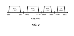
[0022] 図2は、ワイヤレスデバイス110の例示的な実施形態が、そこで動作し得る、3つの例示的なバンドグループを指し示す。ワイヤレスデバイス110は、1000メガヘルツ(MHz)よりも低い周波数をカバーするローバンド(LB)、1000MHzから2300MHzの周波数をカバーするミッドバンド(MB)、および/または2300MHzよりも高い周波数をカバーするハイバンド(HB)において動作し得る。例えば、図2において指し示されるように、ローバンドは698から960MHzをカバーし得、ミッドバンドは1475から2170MHzをカバーし得、およびハイバンドは、2300から2690MHz、ならびに3400から3800MHzをカバーし得る。ローバンド、ミッドバンド、およびハイバンドは、各バンドグループが沢山の周波数バンド(または、単に「バンド」)を含んでいるバンドの3つグループ(またはバンドグループ)を指す。各バンドは、最大200MHzまでカバーし得る。LTEリリース11は、35個のバンドをサポートし、それらはLTE/UMTSバンドと称され、3GPP(登録商標) TS36.101にリストされている。
[0022] FIG. 2 illustrates three exemplary band groups in which an exemplary embodiment of the
[0023] 一般に、任意の数のバンドグループが定義され得る。各バンドグループは、図2において指し示された周波数範囲のいずれかに一致し得る、またはし得ない、周波数の任意の範囲をカバーし得る。各バンドグループは、任意の数のバンドを含み得る。様々な例示的な実施形態において、増幅回路112は、ワイヤレスデバイス110内で信号を増幅するために、様々なバンドグループ内での使用に適している。
[0023] In general, any number of band groups may be defined. Each band group may cover any range of frequencies that may or may not match any of the frequency ranges indicated in FIG. Each band group may include any number of bands. In various exemplary embodiments, the amplifier circuit 112 is suitable for use within various band groups to amplify signals within the
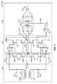
[0024] 図3は、増幅回路300の例示的な実施形態を指し示す。増幅回路300は、図1に指し示される増幅器112としての使用に適している。増幅回路300は、相補的共通ゲート増幅段302、相補的共通ソース増幅段304、および加算回路306を含む。
FIG. 3 illustrates an exemplary embodiment of the
[0025] 相補的共通ゲート増幅段302は、PMOSトランジスタ308、310、およびNMOSトランジスタ312、314を含む。シングルエンドRF入力信号は、入力端子316において受信され、入力端子316は、キャパシタ322および324に接続される。キャパシタ322は、ノード318に接続され、ノード318は、さらにトランジスタ308のソース端子に接続される。キャパシタ324は、ノード320に接続され、ノード320は、さらにトランジスタ314のソース端子に接続される。ノード318は、キャパシタ326を通して信号接地に、および変圧器330の第1の巻き線を通して電圧供給(VDD)に接続される。ノード320は、キャパシタ328を通して、および変圧器330の第2の巻き線を通して信号接地に接続される。同一のgmを送出するように、トランジスタ308およびトランジスタ314も大きさ調整されるので、変圧器330は、(1:1)の比の巻き線を備える。例えば、増幅段302のNMOS側およびPMOS側は、より良いIIP2性能を有するように、対称的に設計される。相補的共通ゲート増幅段302は、ノード348から、反転されていない第1の増幅された出力信号(RF_outp)を出力する。
[0025] The complementary common
[0026] トランジスタ308は、第1の「P」バイアス信号(VBP1)に接続されたゲート端子を有し、トランジスタ310は、第2の「P」バイアス信号(VBP2)に接続されたゲート端子を有する。トランジスタ314は、第1の「N」バイアス信号(VBN1)に接続されたゲート端子を有し、トランジスタ312は、第2の「N」バイアス信号(VBN2)に接続されたゲート端子を有する。
[0027] 相補的共通ソース増幅段304は、PMOSトランジスタ340、342、およびNMOSトランジスタ344、346を含む。トランジスタ340は、キャパシタ332の第1の端子に接続されたゲート端子を有し、キャパシタ332の第2の端子は、ノード318に接続される。トランジスタ340のゲート端子は、抵抗器336の第1の端子に接続され、抵抗器336の第2の端子は、VBP1バイアス信号を受信するように接続される。トランジスタ346は、キャパシタ334の第1の端子に接続されるゲート端子を有し、キャパシタ334の第2の端子は、ノード320に接続される。トランジスタ346のゲート端子はまた、抵抗器338の第1の端子に接続され、抵抗器338の第2の端子は、VBN1バイアス信号を受信するように接続される。トランジスタ342は、VBP2バイアス信号を受信するように接続されたゲート端子を有し、トランジスタ344は、VBN2バイアス信号を受信するように接続されたゲート端子を有する。入力信号から反転された第2の増幅された出力信号(RF_outp)が、ノード350から出力される。
[0027] The complementary common
[0028] 例示的な実施形態において、キャパシタ332、326、328、334、および354は、数ピコファラッド(pF)のオーダーの容量値を有する。抵抗器336および338は、20−40キロ(20k〜40k)オームの範囲内の抵抗値を有する。例示的な実施形態において、図3に指し示されたトランジスタは、所与の電力消費予算に対する選択されたgmの量を提供するように、大きさ調整される。例えば、増幅回路300が、50オームの入力インピーダンスを提供するように設計されると、トランジスタ314のgmおよびトランジスタ308のgmが、各々10mSとなるべく設計され得る。したがって、トランジスタ308および314によって生成される、いかなるノイズや歪みの相殺を容易とするために、トランジスタ346のgmおよびトランジスタ340のgmが、各々10mSとなるべく設計される。
[0028] In the exemplary embodiment,
[0029] 加算回路306は、第1の増幅された出力信号を受信するために、ノード348に接続された第1の巻き線の第1の端子、および第2の増幅された出力信号を受信するために、ノード350に接続された第1の巻き線の第2の端子を有する変圧器352を含む。キャパシタ354は、変圧器352の第1の巻き線を横切って接続されている。変圧器352の第2の巻き線は、(指し示されていない)ダウンコンバーティングミキサ回路に、バランスされた差動RF信号を出力する。例示的な実施形態において、変圧器352は、IF段(たとえば、ベースバンドIFフィルタ)からのノイズを抑制するために、所望の受信機利得および増幅器300およびダウンストリームミキサが提供するように設計された利得量、に依存して設定された巻き線比を備える。
[0029] Summing
[0030] 変圧器352の第1の巻き線のセンタータップは、コンパレータ358の反転されない入力に接続された、共通モード電圧信号(VOCM)を出力する。コンパレータ358の反転される入力は、電圧基準信号(VREF)を受信するように接続される。コンパレータ358の出力端子は、バイアス信号VBN1を出力する。図6に指し示されたコンパレータ358の例示的な実施形態において、コンパレータの出力信号を生成するために、コンパレータ358はまた、バイアス信号VBN2を受信し、利用する。
[0030] The center tap of the first winding of
[0031] 図4は、図3に指し示される増幅回路300とともに用いるバイアス回路400の例示的な実施形態を指し示す。バイアス回路400は、増幅回路300において識別されるバイアス信号を生成する。第1のバイアス回路は、抵抗器406の第1の端子に接続されたソース端子を有するPMOSトランジスタ402を含み、抵抗器406は、電圧供給(VDD)に接続された第2の端子を有する。例示的な実施形態において、抵抗器406は、(1−5)キロオームの範囲中の抵抗値を有する。トランジスタ402は、電流源408の第1の端子に接続された、ドレイン端子を有し、電流源408は、信号接地に接続される第2の端子を有する。例示的な実施形態において、電流源408は、おおよそ0.1ミリアンペアの電流を提供する。例えば、例示的な実施形態において、電流源408(および実施形態において指し示された他の電流源)は、所望の電流量を提供する電流源として振る舞うために、飽和領域で動作するNMOSトランジスタである。トランジスタ402のゲート端子は、ドレイン端子に接続され、また、バイアス信号VBP2を出力する。
[0031] FIG. 4 illustrates an exemplary embodiment of a
[0032] 第2のバイアス回路は、抵抗器412の第1の端子に接続されたソース端子を有するNMOSトランジスタ404を含み、(たとえば、1−5キロオームの)抵抗器412は、信号接地に接続された第2の端子を有する。トランジスタ404は、電流を受領するために、電流源410の第1の端子に接続されたドレイン端子を有し、電流源410は、電圧供給(VDD)に接続された第2の端子を有する。例示的な実施形態において、電流源410は、おおよそ0.1ミリアンペアの電流を供給する。トランジスタ404のゲート端子は、ソース端子に接続され、また、バイアス信号VBN2を出力する。
[0032] The second bias circuit includes an
[0033] 図5は、図3に指し示される増幅回路300とともに使用されるバイアス回路500の例示的な実施形態を指し示す。バイアス回路500は、増幅回路300において識別されたバイアス信号を生成する。バイアス回路500は、PMOSトランジスタ502および504を含む。トランジスタ502は、電圧供給(VDD)に接続されたソース端子、およびトランジスタ504のソース端子に接続されたドレイン端子を有する。トランジスタ502のゲート端子は、トランジスタ504のドレイン端子に接続され、また、バイアス信号VBP1を出力する。トランジスタ504のゲート端子は、図4で指し示されるトランジスタ402から出力されるバイアス信号VBP2を受信する。トランジスタ504のドレイン端子は、電流源506の第1の端子に接続され、電流源506は、信号接地に接続される第2の端子を有する。例示的な実施形態において、電流源506は、おおよそ0.1ミリアンペアの電流を供給する。
[0033] FIG. 5 illustrates an exemplary embodiment of a
[0034] 図6は、図3に指し示されるコンパレータ358の詳しい例示的な実施形態を指し示す。コンパレータ358は、VBN2信号、電圧基準信号(VREF)、および共通モード電圧信号(VOCM)を受信し、バイアス信号VBN1を生成する。例示的な実施形態において、VREF信号は、VDD/2の値を有する。VREF信号は、一連の抵抗器を通して流れる電流源を使用することによって、またはVDDおよびGND間に接続された抵抗分割器を使用することによって、生成することができる。
[0034] FIG. 6 illustrates a detailed exemplary embodiment of the
[0035] コンパレータ358は、電流信号を受信するために、電流源602の第1の端子に接続されたソース端子、を有するPMOSトランジスタ604、606のペアーを含む。電流源602の第2の端子は、電圧供給(VDD)に接続される。例示的な実施形態において、電流源602は、おおよそ0.2ミリアンペアの電流を供給する。トランジスタ604は、電圧基準信号(VREF)を受信するように接続されたゲート端子を有する。トランジスタ606は、共通モード電圧信号(VOCM)を受信するように接続されたゲート端子を有する。
[0035]
[0036] トランジスタ604、606のドレイン端子は、第1のNMOSトランジスタペアー608、610のドレイン端子に接続される。トランジスタ604、606のドレイン端子はまた、第2のNMOSトランジスタペアー612、614のゲート端子に接続される。トランジスタ608、610は、トランジスタ612、614のドレイン端子に接続されたソース端子を有する。トランジスタ612、614は、信号接地に接続されたソース端子を有する。トランジスタ612のゲート端子は、バイアス信号VBN1を出力する。トランジスタ608、610のゲート端子は、図4で指し示されるトランジスタ404から出力される、バイアス信号VBN2を受信する。例示的な実施形態において、コンパレータ358は、段302、304および加算回路306によって形成されたクローズドフィードバックループのための所望の利得量を提供する。
The drain terminals of the
[0037] 図7は、利得制御を含むように拡張された増幅回路300の、詳しい例示的な実施形態を指し示す。例えば、図7に指し示されるように、破線768は、相補的共通ゲート増幅段302と、相補的共通ソース増幅段304とを分離する。相補的共通ゲート増幅段302は、電流分流器702を含むように拡張され、相補的共通ソース増幅段304は、電流スライサ704を含むように拡張される。図7において指し示される増幅回路の利得を設定するように、電流分流器702および電流スライサ704の動作を制御するための制御信号を出力すべく、コントローラ764が提供される。明瞭さのために、図7には、加算回路306は指し示されていないが、図7に指し示された増幅回路の一部として、上記で説明されたように動作する。
[0037] FIG. 7 illustrates a detailed exemplary embodiment of an
[0038] 例示的な実施形態において、相補的共通ゲート増幅段302のトランジスタ310、312は、電流分流器702で置き換えられる。電流分流器702は、2つのPMOSトランジスタグループ、および2つのNMOSトランジスタグループを含む。PMOSトランジスタの第1のグループは、PMOSトランジスタ706、708、および710を含む。トランジスタ706、708、および710は、トランジスタ308のドレイン端子に接続されたソース端子を有し、ノード756に接続されたドレイン端子を有し、ノード756はまた、(たとえば、1−5キロオームの)抵抗器758の第1の端子に接続される。(反転されていない)出力信号RF_OUTPは、ノード756から出力される。トランジスタ706、708、および710は、コントローラ764によって生成される制御信号D1、D2、およびD3を、それぞれ受信するように接続されたゲート端子を有する。
[0038] In the exemplary embodiment,
[0039] PMOSトランジスタの第2のグループは、PMOSトランジスタ712、714、および716を含む。トランジスタ712、714、および716は、トランジスタ308のドレイン端子に接続されたソース端子を有し、また、ノード760に接続されたドレイン端子を有する。ノード760は、抵抗器758の第2の端子、およびキャパシタ762の第1の端子に接続され、キャパシタ762は、信号接地に接続された第2の端子を有する。例示的な実施形態において、所望の周波数範囲で、ダウンストリームミキサに匹敵するインピーダンスを提供するように、キャパシタ762は、大きさ調整される。トランジスタ712、714、および716は、コントローラ764によって生成される制御信号D4、D5、およびD6を、それぞれ受信するように接続されたゲート端子を有する。
[0039] The second group of PMOS transistors includes
[0040] NMOSトランジスタの第1のグループは、NMOSトランジスタ718、720、および722を含む。トランジスタ718、720、および722は、トランジスタ314のドレイン端子に接続されたソース端子を有し、また、ノード756に接続されたドレイン端子を有する。トランジスタ718、720、および722は、コントローラ764によって生成される制御信号D7、D8、およびD9を、それぞれ受信するように接続されたゲート端子を有する。
[0040] The first group of NMOS transistors includes
[0041] NMOSトランジスタの第2のグループは、NMOSトランジスタ724、726、および728を含む。トランジスタ724、726、および728は、トランジスタ314のドレイン端子に接続されたソース端子を有し、また、ノード760に接続されたドレイン端子を有する。トランジスタ724、726、および728は、コントローラ764によって生成される制御信号D10、D11、およびD12を、それぞれ受信するように接続されたゲート端子を有する。
[0041] A second group of NMOS transistors includes
[0042] 例示的な実施形態において、電流分流器702のNMOSおよびPMOSトランジスタのトランジスタグループは、「M」の表示を有し、「M」は、トランジスタについてのフィンガーの数(たとえば、トランジスタのための乗数)を示す。例えば、トランジスタ312がW(um)の幅を有する場合、トランジスタ718は、W/4に大きさ調整され、トランジスタ720は、W/2に大きさ調整され、トランジスタ722は、W/4に大きさ調整される。よって、グループは、置き換えられたトランジスタについて、1:2:1の比を提供するように、大きさ調整される。電流分流器702の全てのトランジスタグループについても、同様のことが当てはまる。トランジスタについて、他の大きさまたは比が使用され得ることにも、留意すべきである。
[0042] In an exemplary embodiment, the NMOS and PMOS transistor transistor group of
[0043] 例示的な実施形態において、相補的共通ソース増幅段304のトランジスタ340、342、344、および346は、電流スライサ704で置き換えられる。電流スライサ704は、コントローラ764によって選択的にイネーブルでき得る多数の分岐を含む。第1の分岐は、PMOSトランジスタ730および732と、NMOSトランジスタ734および736とを含む。トランジスタ730は、電圧供給(VDD)に接続されたソース端子、およびトランジスタ732のソース端子に接続されたドレイン端子を有する。トランジスタ730は、キャパシタ332の第1の端子に接続されたゲート端子を有する。
[0043] In the exemplary embodiment,
[0044] トランジスタ732は、トランジスタ734のドレイン端子およびノード754に接続されたドレイン端子を有し、トランジスタ754は、増幅された出力信号RF_OUTNを出力する。トランジスタ730は、コントローラ764によって生成される制御信号B1に接続されたゲート端子を有する。
[0045] トランジスタ734は、トランジスタ736のドレイン端子に接続されたソース端子を有する。トランジスタ734は、コントローラ764によって生成される制御信号B4に接続されたゲート端子を有する。
[0046] トランジスタ736は、信号接地に接続されたソース端子を有する。トランジスタ736は、キャパシタ334の第1の端子に接続されたゲート端子を有する。
[0046]
[0047] 第2の分岐は、トランジスタ738、740、742、および744を含む。第3の分岐は、トランジスタ746、748、750、および752を含む。第2および第3の分岐は、同様に第1の分岐に接続される。制御信号B2およびB5は、第2の分岐を制御し、制御信号B3およびB6は、第3の分岐を制御する。
[0047] The second branch includes
[0048] 例示的な実施形態において、電流スライサ704のトランジスタのトランジスタ分岐は、「M」の表示を有し、「M」は、トランジスタについてのフィンガーの数(たとえば、トランジスタのための乗数)を示す。例えば、トランジスタ340がW(um)の幅を有する場合、トランジスタ730は、W/4に大きさ調整され、トランジスタ738は、W/2に大きさ調整され、トランジスタ746は、W/4に大きさ調整される。よって、トランジスタは、置き換えられたトランジスタについて、1:2:1の比を提供するように、大きさ調整される。電流スライサ704の全てのトランジスタグループについても、同様のことが当てはまる。トランジスタについて、他の大きさまたは比が使用され得ることにも、留意すべきである。
[0048] In an exemplary embodiment, the transistor branch of the transistor of
[0049] コントローラ764は、CPU、プロセッサ、ゲートアレイ、ハードウェアロジック、ディスクリート回路、メモリ要素、および/またはハードウェア実行ソフトウェアのうちの少なくとも1つを備える。コントローラ764はまた、命令、制御情報、データ、構成パラメータ、測定、および/または他の情報、のような構成情報を受信するために、通信線766を使用して、ワイヤレスデバイスにおいて、他のエンティティと通信するように構成される。コントローラ764は、図7において指し示された増幅回路の利得を設定するために、電流分流器702および電流スライサ704の動作を制御すべく、制御信号D(n)およびB(n)を生成するために、受信した構成情報を使用する。
[0049] The
[0050] 図7において指し示された増幅回路の入力インピーダンスは、利得設定が変化しても、変わらないことにも留意すべきである。例えば、入力インピーダンスは、式[1/(トランジスタ314のgm+トランジスタ308のgm)]によって決定される。利得が変化されるとき、トランジスタ314およびトランジスタ308の動作条件は、最高利得条件下とぴったり同一のままである。よって、利得が変化されるとき、トランジスタ314からのドレイン電流だけが、電流分流器(718、720、722、724、726、および728)中のトランジスタ間に分流され、分流は、入力インピーダンスには影響を及ぼさない。トランジスタ308を含むPMOS側についても、同様のことが当てはまる。それゆえ、如何に利得が変化されようとも、入力インピーダンスは同一のままであり、これは、正確な利得ステップを提供する。増幅器700の利得を設定するために、如何に、コントローラ764、電流分流器702、および電流スライサ704が動作するかの詳しい説明が、以下に提供される。
[0050] It should also be noted that the input impedance of the amplifier circuit indicated in FIG. 7 does not change as the gain setting changes. For example, the input impedance is determined by the equation [1 / (gm of
[0051] 図8は、図7において指し示された増幅回路の利得を設定するための電流分流器702の動作を例証する。動作の間中、(図8中には指し示されない)コントローラ764は、電流分流器702のトランジスタを選択的にイネーブルまたはディセーブルするために、D(n)制御信号を出力する。例えば、コントローラ764は、受信した構成情報に基づいて、制御信号D(n)の状態を決定する。この例証のために、太字で指し示されたトランジスタ708、714、720、および726を、それぞれイネーブルするために、コントローラ764は、制御信号D2、D5、D8、およびD11がアクティブ状態となるように、出力することが想定されるであろう。電流分流器702の残りのトランジスタをディセーブルするために、残りのD(n)制御信号は、非アクティブ状態に設定される。
[0051] FIG. 8 illustrates the operation of
[0052] RF入力が高レベルになるとき、トランジスタ308は、バイアス信号VBP1によってイネーブルでき、また、トランジスタ314は、ディセーブルされる。トランジスタ308がRF入力およびバイアス信号VBP1によってイネーブルされるとき、電流Iは、トランジスタ308を通して流れ、2つの信号経路を通して分流される。電流I1は、イネーブルされたトランジスタ708を通して、第1の信号経路で流れ、電流I2は、イネーブルされたトランジスタ714を通して、第2の信号経路で流れる。電流I1は、ノード756まで流れ、出力として利用可能である。電流I2は、キャパシタ762まで、および信号接地まで流れる。よって、出力ノード756から電流を離れて分流するように電流分流器を調整することによって、増幅段302の利得は設定できる。同様の動作は、RF入力が低レベルになり、したがって、トランジスタ308がディセーブルされ、トランジスタ314がイネーブルされたときに生じる。このケースにおいて、電流I1は、トランジスタ720を通して出力から流れ、I2に等しい電流が、キャパシタ762からトランジスタ726を通して流れ、トランジスタ314を通して流れる電流Iが形成される。
[0052] When the RF input goes high,
[0053] コントローラ764は、電流分流器702のトランジスタを通して、電流Iを分流した結果として、様々な利得設定が得られるように、電流分流器702における、任意のトランジスタをイネーブルまたはディセーブルするためのD(n)制御信号を出力できる。よって、より多くのトランジスタがイネーブルされて、より多くの電流が出力に分流し、より少ないトランジスタがイネーブルされて、より少ない電流がキャパシタ762に分流するとき、利得は増加する。より少ないトランジスタがイネーブルされて、より少ない電流が出力に分流され、より多くのトランジスタがイネーブルされて、より多くの電流がキャパシタ762に分流するとき、利得は減少する。
[0053] The
[0054] 図9は、図7に指し示された増幅回路の利得を設定するための、電流スライサ704の動作を例証する。動作の間中、(図9中には指し示されない)コントローラ764は、電流スライサ704のトランジスタの分岐を選択的にイネーブルまたはディセーブルするために、B(n)制御信号を出力する。例えば、コントローラ764は、受信した構成情報に基づいて、制御信号B(n)の状態を決定する。この例証のために、それぞれ太字で指し示されたトランジスタ738、740、742、および744を含む1つの分岐をイネーブルするために、コントローラ764は、制御信号B2およびB5がアクティブ状態となるように、出力することが想定されるであろう。電流分流器704のトランジスタの残りの分岐をディセーブルするために、残りのB(n)制御信号は、非アクティブ状態に設定される。
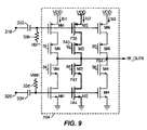
[0054] FIG. 9 illustrates the operation of
[0055] B2およびB5制御信号によって、トランジスタ740および742がイネーブルされるとき、電流Ib2は、トランジスタ738、740、742、および744を通して流れることができる。残りのB(n)制御信号が、他の分岐におけるトランジスタをディセーブルするので、電流Ib1およびIb3は、それらの分岐において流れることが、妨げられる。ノード318における、RF入力が低(または、マイナスの)電圧レベルの間、トランジスタ738はイネーブルされ、電流Ib2が、(B2によってイネーブルされた)トランジスタ740を通して、ノード754まで流れ、反転されたRF_OUTN信号を生成する出力が入手可能である。ノード320におけるRF入力信号の低(または、マイナス)電圧レベルは、信号接地への電流の流れを妨げるために、トランジスタ744をディセーブルする。代替的に、ノード318における、RF入力が高(または、プラスの)電圧レベルの間、電流Ib2は、ターンオフされたトランジスタ738を通して、ノード754まで流れない。しかしながら、対応する、ノード320におけるRF入力高(または、プラスの)電圧レベルは、トランジスタ744をイネーブルし、電流Ib2が、ノード754から信号接地まで流れるようにし、それにより、反転されたRF_OUTN信号を生成する。
[0055] When
[0056] よって、1つまたは複数の分岐を活性化し、出力ノード756、ヘ/から電流が流れるように電流スライサ704を調整することによって、増幅段304の利得は設定できる。コントローラ764は、様々な利得設定を得ることができるように、電流スライサ704におけるトランジスタの分岐をイネーブルまたはディセーブルするために、B(n)制御信号を出力できる。例えば、第1、第2および第3の分岐の任意の組み合わせは、電流Ib1、Ib2、およびIb3が、それぞれの分岐を通して流れるか、否かを制御するために、イネーブルまたはディセーブルできる。さらに、電流スライサ704の1つまたは複数の分岐がディセーブルされたとき、対応する電流の節約の結果となる。
Thus, by activating one or more branches and adjusting the
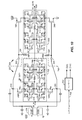
[0057] 図10は、利得制御を含むように拡張された増幅回路300の詳しい例示的、代替的実施形態を指し示す。例えば、増幅段302は、電流分流器702を含むように拡張され、上記で説明されたように、電流分流器702は、相補的共通ゲート増幅段302の利得を設定するように動作する。相補的共通ソース増幅段304は、電流分流器1000を含むように拡張され、電流分流器1000は、電流分流器702と同様に利得を設定するように動作する。コントローラ764は、電流分流器702および電流分流器1000の動作を制御するために、制御信号D(n)およびD’(n)を出力する。
[0057] FIG. 10 illustrates a detailed exemplary, alternative embodiment of an
[0058] 例示的な実施形態において、相補的共通ソース増幅段304のトランジスタ342、344は、電流分流器1000で置き換えられる。電流分流器1000は、PMOSトランジスタの2つのグループ、およびNMOSトランジスタの2つのグループを含む。PMOSトランジスタの第1のグループは、トランジスタ1002、1004、および1006を含む。トランジスタ1002、1004、および1006は、トランジスタ340のドレイン端子に接続されたソース端子を有し、ノード760に接続されたドレイン端子を有し、ノード760はまた、(たとえば、1−5キロオームの)抵抗器1026の第1の端子に接続される。反転された出力信号RF_OUTNは、ノード1028から出力され、ノード1028は、抵抗器1026の第2の端子に接続される。トランジスタ1002、1004、および1006は、コントローラ764によって生成される制御信号D’1、D’2、およびD’3を、それぞれ受信するように接続されたゲート端子を有する。
In the exemplary embodiment,
[0059] PMOSトランジスタの第2のグループは、トランジスタ1008、1010、および1012を含む。トランジスタ1008、1010、および1012は、トランジスタ340のドレイン端子に接続されたソース端子を有し、また、ノード1028に接続されたドレイン端子を有する。ノード1028は、抵抗器1026の第2の端子に接続される。トランジスタ1008、1010、および1012は、コントローラ764によって生成される制御信号D’4、D’5、およびD’6を、それぞれ受信するように接続されたゲート端子を有する。
[0059] A second group of PMOS transistors includes
[0060] NMOSトランジスタの第1のグループは、トランジスタ1014、1016、および1018を含む。トランジスタ1014、1016、および1018は、トランジスタ346のドレイン端子に接続されたソース端子を有し、また、ノード760に接続されたドレイン端子を有する。トランジスタ1014、1016、および1018は、コントローラ764によって生成される制御信号D’7、D’8、D’9を、それぞれ受信するように接続されたゲート端子を有する。
[0060] The first group of NMOS transistors includes
[0061] NMOSトランジスタの第2のグループは、トランジスタ1020、1022、および1024を含む。トランジスタ1020、1022、および1024は、トランジスタ346のドレイン端子に接続されたソース端子を有し、また、ノード1028に接続されたドレイン端子を有する。トランジスタ1020、1022、および1024は、コントローラ764によって生成される制御信号D’10、D’11、D’12を、それぞれ受信するように接続されたゲート端子を有する。
[0061] A second group of NMOS transistors includes
[0062] 図11は、図10において指し示された増幅器の利得を設定するための、電流分流器702および1000の動作を例証する。動作の間中、コントローラ764は、電流分流器702のトランジスタを、選択的にイネーブルまたはディセーブルするために、D(n)制御信号を出力する。例えば、コントローラ764は、受信した構成情報に基づいて、制御信号D(n)の状態を決定する。この例証のために、太字で指し示されたトランジスタ708、714、720、および726を、それぞれイネーブルするために、コントローラ764は、制御信号D2、D5、D8、およびD11がアクティブ状態となるように、出力することが想定されるであろう。電流分流器702の残りのトランジスタをディセーブルするために、残りのD(n)制御信号は、非アクティブ状態に設定される。
[0062] FIG. 11 illustrates the operation of the
[0063] コントローラ764はまた、電流分流器1000のトランジスタを、選択的にイネーブルまたはディセーブルするために、D’(n)制御信号を出力する。例えば、コントローラ764は、受信した構成情報に基づいて、制御信号D’(n)の状態を決定する。この例証のために、太字で指し示されたトランジスタ1004、1010、1016、および1022を、それぞれイネーブルするために、コントローラ764は、制御信号D’2、D’5、D’8、およびD’11がアクティブ状態となるように、出力することが想定されるであろう。電流分流器1000の残りのトランジスタをディセーブルするために、残りのD’(n)制御信号は、非アクティブ状態に設定される。
[0063] The
[0064] 上記で説明されたように設定された制御信号で、RF入力信号が、低になるとき、トランジスタ314および340はイネーブルされ、トランジスタ308および346はディセーブルされる。電流スライサ702において、電流は、矢印で示されるように、イネーブルされたトランジスタ720および726を通して流れる。ノード760から流れる電流(Ia)は、イネーブルされたトランジスタ726を通して流れる。電流スライサ1000において、電流は、矢印で示されるように、イネーブルされたトランジスタ1004および1010を通して流れる。ノード760に流れ込む電流(Ib)は、イネーブルされたトランジスタ1004を通して流れる。
[0064] When the RF input signal goes low with the control signal set as described above,
[0065] この例示的な実施形態において、ノード760は、仮想的AC信号接地を形成する。このノードにおいて、電流IaおよびIbは、反対方向に流れる。少量の電流が、キャパシタ762を通して流れ得る。しかしながら、この少量の電流のため、キャパシタ762は、サイズが小さいであろう。例えば、キャパシタ762は、加算回路の入力インピーダンスに匹敵するインピーダンスを提供するのに十分な大きさであればよい。例示的な実施形態において、加算回路は受動的ネットワークであり、それゆえ、図11に指し示された増幅回路に結合されたダウンストリームミキサの入力インピーダンスを反映するだけである。
[0065] In this exemplary embodiment,
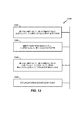
[0066] 図12は、図7および図10において指し示された増幅回路の例示的実施形態によって実行される、例示的な動作を指し示す。例えば、例示的な実施形態において、図7において指し示された増幅回路は、図1において指し示されたワイヤレスデバイス110のようなデバイス中で、増幅された信号を生成するための動作1200を実行する。
[0066] FIG. 12 illustrates exemplary operations performed by the exemplary embodiment of the amplifier circuit indicated in FIGS. For example, in the exemplary embodiment, the amplifier circuit indicated in FIG. 7 performs
[0067] 動作1202の間中、差動出力の第1の増幅された信号を生成するために、入力信号の増幅が実行される。増幅は、信号反転を伴わずに実行される。例えば、相補的共通ゲート増幅段702が、この動作を実行する。
[0067] During
[0068] 動作1204の間中、第1の増幅された信号を生成するために使用される増幅利得は、電流分流を使用して設定される。例えば、コントローラ764は、この動作を実行するために、電流分流器702のトランジスタを制御する制御信号D(n)を出力する。
[0068] During
[0069] 動作1206の間中、差動出力の第2の増幅された信号を生成するために、入力信号の増幅が実行される。増幅は、信号反転を伴って実行される。例えば、相補的共通ソース増幅段704が、この動作を実行する。
[0069] During
[0070] 動作1208の間中、第2の増幅された信号を生成するために使用される増幅利得は、電流スライシングを使用して設定される。例えば、コントローラ764は、この動作を実行するために、電流スライサ704のトランジスタを制御する制御信号B(n)を出力する。代替的に、電流分流器1000が、この動作を実行するために使用される。
[0070] During
[0071] したがって、図7および図10において指し示された増幅回路は、上記で説明された動作を実行する。動作1200は、例示的であり、動作1200への軽微な変化、変更、再配列、および他の変化は、例示的な実施形態の範囲内であるであることに留意すべきである。
Therefore, the amplifier circuit indicated in FIGS. 7 and 10 performs the operation described above. It should be noted that
[0072] 図13は、増幅装置1300の例示的な実施形態を指し示す。例示的な実施形態において、装置1300は、図7で指し示される増幅回路400としての使用に適している。
FIG. 13 illustrates an exemplary embodiment of an
[0073] 装置1300は、第1の出力端子における第1の増幅された信号を生成するために、入力端子における入力信号を増幅する第1の手段(1302)を含み、第1の手段は、例示的な実施形態において、図7において指し示された増幅段302を備える。
[0073] The
[0074] 装置1300はまた、増幅する手段の利得を設定するために、入力信号に応答して生成された電流を分流する第2の手段(1304)を備え、第2の手段は、例示的な実施形態において、電流分流器702を備える。
[0074] The
[0075] 装置1300はまた、第2の出力端子において第2の増幅された信号を生成するために、入力端子における信号を増幅するように構成された、信号反転を伴う、増幅する第3の手段(1306)を備え、第3の手段は、例示的な実施形態において、図7において指し示された増幅段304を備える。
[0075] The
[0076] 装置1300はまた、信号反転を伴う、増幅する手段の利得を設定する第4の手段(1308)を備え、第4の手段は、例示的な実施形態において、電流スライサ704または電流分流器1000を備える。
[0076] The
[0077] 本明細書で説明される増幅回路の例示的な実施形態は、IC、アナログIC、RFIC、混合信号IC、ASIC、プリント回路基板(PCB)、電子デバイス、等、上に実装され得る。増幅回路の例示的な実施形態はまた、相補型金属酸化膜半導体(CMOS)、NチャネルMOS(NMOS)、PチャネルMOS(PMOS)、バイポーラ接合トランジスタ(BJT)、バイポーラCMOS(BiCMOS)、シリコンゲルマニウム(SiGe)、ガリウムヒ素(GaAs)、ヘテロ接合バイポーラトランジスタ(HBT)、高電子移動度トランジスタ(HEMT)、シリコン・オン・インシュレータ(SOI)、等のような、様々なIC処理技術を用いて作られ得る。 [0077] Exemplary embodiments of amplifier circuits described herein may be implemented on an IC, analog IC, RFIC, mixed signal IC, ASIC, printed circuit board (PCB), electronic device, etc. . Exemplary embodiments of amplifier circuits also include complementary metal oxide semiconductor (CMOS), N-channel MOS (NMOS), P-channel MOS (PMOS), bipolar junction transistor (BJT), bipolar CMOS (BiCMOS), silicon germanium. (SiGe), gallium arsenide (GaAs), heterojunction bipolar transistor (HBT), high electron mobility transistor (HEMT), silicon-on-insulator (SOI), etc. Can be.
[0078] 本明細書で説明される増幅回路の例示的な実施形態を実装する装置は、独立型(stand-alone)デバイスであり得、またはより大きなデバイスの一部分であり得る。デバイスは、(i)独立型IC、(ii)データおよび/または命令を格納するためのメモリICを含み得る、1つまたは複数のICのセット、(iii)RF受信機(RFR)またはRF送信機/受信機(RTR)のようなRFIC、(iv)移動局モデム(MSM)のようなASIC、(v)他のデバイス内に埋め込まれ得るモジュール、(vi)受信機、セルラー電話、ワイヤレスデバイス、ハンドセット、または移動体ユニット、(vii)等、であり得る。 [0078] An apparatus implementing an exemplary embodiment of the amplifier circuit described herein may be a stand-alone device or may be part of a larger device. The device may include (i) a stand-alone IC, (ii) a memory IC for storing data and / or instructions, a set of one or more ICs, (iii) an RF receiver (RFR) or an RF transmission RFICs such as receiver / receiver (RTR), (iv) ASICs such as mobile station modem (MSM), (v) modules that can be embedded in other devices, (vi) receivers, cellular phones, wireless devices , Handset, or mobile unit, (vii) and the like.
[0079] 1つまたは複数の例示的な設計において、説明された機能は、ハードウェア、ファームウェア、またはそれらの任意の組み合わせで実装され得る。ソフトウェアを実行するハードウェアによって実装される場合、機能は、1つまたは複数の命令またはコードとして、コンピュータ可読媒体上に記憶され、または、コンピュータ可読媒体を介して送信され得る。コンピュータ可読媒体は、コンピュータ記憶媒体と、1つの場所から別の場所へのコンピュータプログラムの転送を容易にする任意の媒体を含む通信媒体との両方を含む。記憶媒体は、コンピュータによってアクセスされることができる任意の利用可能な媒体であり得る。限定ではなく例として、そのようなコンピュータ可読媒体は、RAM、ROM、EEPROM(登録商標)、CD−ROMまたは他の光ディスク記憶装置、磁気ディスク記憶装置または他の磁気記憶デバイス、あるいは命令もしくはデータ構造の形で、所望のプログラムコードを搬送または記憶するために使用されることができ、コンピュータによってアクセスされることができる任意の他の媒体を備えることができる。また、任意の接続は、適切にコンピュータ可読媒体と称される。例えば、ソフトウェアがウェブサイト、サーバ、または他の遠隔ソースから、同軸ケーブル、光ファイバーケーブル、ツイストペア、デジタル加入者回線(DSL)、あるいは赤外線、無線、およびマイクロ波のようなワイヤレス技術を使用して送信される場合、同軸ケーブル、光ファイバーケーブル、ツイストペア、DSL、あるいは赤外線、無線、およびマイクロ波のようなワイヤレス技術は媒体の定義に含まれている。ディスク(disk)およびディスク(disc)は、本明細書で使用される場合、コンパクトディスク(disc)(CD)、レーザーディスク(登録商標)(disc)、光ディスク(disc)、デジタル多用途ディスク(disc)(DVD)、フロッピー(登録商標)ディスク(disk)およびBlu−ray(登録商標)ディスク(disc)を含み、ここで、ディスク(disk)は通常、磁気的にデータを再生し、その一方でディスク(disc)は、レーザーを用いて光学的にデータを再生する。上記の組み合わせも、コンピュータ可読媒体の範囲内に含まれるべきである。 [0079] In one or more exemplary designs, the functions described may be implemented in hardware, firmware, or any combination thereof. If implemented by hardware executing software, the functions may be stored on or transmitted over as one or more instructions or code on a computer-readable medium. Computer-readable media includes both computer storage media and communication media including any medium that facilitates transfer of a computer program from one place to another. A storage media may be any available media that can be accessed by a computer. By way of example, and not limitation, such computer readable media can be RAM, ROM, EEPROM®, CD-ROM or other optical disk storage device, magnetic disk storage device or other magnetic storage device, or instructions or data structure. In the form of any other medium that can be used to carry or store the desired program code and that can be accessed by a computer. Also, any connection is properly termed a computer-readable medium. For example, software transmits from a website, server, or other remote source using coaxial cable, fiber optic cable, twisted pair, digital subscriber line (DSL), or wireless technologies such as infrared, wireless, and microwave Where applicable, coaxial cable, fiber optic cable, twisted pair, DSL, or wireless technologies such as infrared, radio, and microwave are included in the definition of media. Disc and disc as used herein are compact disc (CD), laser disc (registered trademark), optical disc (disc), digital versatile disc (disc) ) (DVD), floppy® disk and Blu-ray® disc, where the disk typically reproduces data magnetically while A disc optically reproduces data using a laser. Combinations of the above should also be included within the scope of computer-readable media.
[0080] 本開示の先の説明は、当業者が本開示を製造または使用することを可能にするために提供される。本開示に対する様々な変更は、当業者にとって容易に明らかであり、ここで定義された一般的な原則は、本開示の範囲から逸脱することなく他の変形に適用され得る。よって、本開示は、本明細書において説明された例および設計に限定されるように意図されず、本明細書で開示された原理および新規の特徴と一致する、最も幅広い範囲が付与されるべきである。 [0080] The previous description of the disclosure is provided to enable any person skilled in the art to make or use the disclosure. Various modifications to the present disclosure will be readily apparent to those skilled in the art, and the general principles defined herein may be applied to other variations without departing from the scope of the present disclosure. Thus, this disclosure is not intended to be limited to the examples and designs described herein, but is to be accorded the widest scope consistent with the principles and novel features disclosed herein. It is.
[0080] 本開示の先の説明は、当業者が本開示を製造または使用することを可能にするために提供される。本開示に対する様々な変更は、当業者にとって容易に明らかであり、ここで定義された一般的な原則は、本開示の範囲から逸脱することなく他の変形に適用され得る。よって、本開示は、本明細書において説明された例および設計に限定されるように意図されず、本明細書で開示された原理および新規の特徴と一致する、最も幅広い範囲が付与されるべきである。
以下に、本出願時の特許請求の範囲に記載された発明を付記する。
[付記1] 第1の増幅された信号を生成するために、入力端子における入力信号を増幅するように構成された第1の増幅段と、前記第1の増幅段は、前記第1の増幅段の利得を設定するために、第1の電流を選択的に分流するように構成された電流分流器を有し、
第2の増幅された信号を生成するために、前記入力端子における前記入力信号を増幅するように構成された第2の増幅段と、前記第2の増幅段は、前記第2の増幅段の利得を設定するための利得制御回路を有する、を備える、装置。
[付記2] 前記第1の増幅段は、前記入力信号に関して反転されていない、前記第1の増幅された信号を生成する相補的共通ゲート(CCG)増幅器として構成され、前記第2の増幅段は、前記入力信号に関して反転されている、前記第2の増幅された信号を生成する相補的共通ソース(CCS)増幅器として構成された、付記1の装置。
[付記3] 前記利得制御回路は、前記第2の増幅段の前記利得を設定するために、選択的にイネーブルされる相補的カスコードトランジスタの並列分岐を備える、付記2の装置。
[付記4] 前記第1の増幅段の前記利得を設定するために、前記電流分流器を制御し、また、前記第2の増幅段の前記利得を設定するために、前記利得制御回路を制御すべく、制御信号を出力するように構成されたコントローラを、さらに備える、付記3の装置。
[付記5] 前記コントローラは、選択された利得設定に前記第1の増幅段の前記利得を設定するために、AC接地を形成するノードに、前記第1の電流の選択された量を分流する、前記電流分流器を制御するための第1の制御信号を出力するように構成され、また、前記コントローラは、前記選択された利得設定に前記第2の増幅段の前記利得を設定するために、
前記相補的カスコードトランジスタの前記並列分岐を選択的にイネーブルすべく、第2の制御信号を出力するように構成された、付記4の装置。
[付記6] 前記利得制御回路は、前記第2の増幅段の前記利得を設定するために、第2の電流の選択された量を分流するように構成された第2の電流分流器を備える、付記1の装置。
[付記7] 前記電流分流器は、前記第1の電流の選択された量をノードに分流するように構成され、また、前記第2の電流分流器は、前記第2の電流の前記選択された量を前記ノードに分流するように構成され、前記ノードはAC信号接地を形成する、付記6の装置。
[付記8] 前記ノードおよび信号接地間に結合されたキャパシタをさらに備え、前記ノードにおいて、前記第1および第2の電流の前記選択された量は、反対方向に流れ、結果として、前記第1または第2の電流よりも小さい第3の電流が、前記ノードおよび前記キャパシタ間に流れる、付記7の装置。
[付記9] 前記第1の増幅段の前記利得を設定するために、前記電流分流器を制御し、また、前記第2の増幅段の前記利得を設定するために、前記第2の電流分流器を制御すべく、制御信号を出力するように構成されたコントローラを、さらに備える、付記7の装置。
[付記10] 前記第1および第2の増幅された信号を受信し、差動信号を出力するように構成された加算回路を、さらに備える、付記1の装置。
[付記11] 前記加算回路は、前記第1および第2の増幅段をバイアスする、バイアス信号を生成するバイアス信号ジェネレータを備える、付記10の装置。
[付記12] 前記加算回路は、第1の巻き線を横切る前記第1および第2の増幅された信号を受信する変圧器を備え、前記第1の巻き線は、前記バイアス信号ジェネレータに共通モード電圧信号を出力するセンタータップを有する、付記11の装置。
[付記13] 第1の出力端子において第1の増幅された信号を生成するために、入力端子における入力信号を増幅する手段と、前記第1の増幅された信号は、前記入力信号に関して反転されておらず、
前記増幅する手段の利得を設定するために、前記入力信号に応答して生成された、第1の電流を分流する手段と、
第2の出力端子において第2の増幅された信号を生成するために、前記入力端子における前記信号を増幅するように構成された、信号反転を有する、増幅する手段と、
信号反転を有する、前記増幅する手段の利得を設定する手段と
を備える装置。
[付記14] 前記利得を設定する手段は、信号反転を有する、前記増幅する手段の前記利得を設定するために、選択的にイネーブルされる相補的カスコードトランジスタの並列分岐を備える、付記13の装置。
[付記15] 前記増幅する手段は、前記第1の増幅された信号を生成する相補的共通ゲート(CCG)増幅器を備える、付記13の装置。
[付記16] 前記増幅する手段は、前記第2の増幅された信号を生成する相補的共通ソース(CCS)増幅器を備える、付記13の装置。
[付記17] 前記第1の電流を分流する手段は、前記第1の電流の選択された部分を、AC信号接地を形成するノードに向けるように構成された、付記13の装置。
[付記18] 前記ノードおよび信号接地間に結合されたキャパシタ、をさらに備える、付記17の装置。
[付記19] 前記利得を設定する手段は、信号反転を有する前記増幅する手段の前記利得を設定するために、第2の電流を分流する手段を備える、付記13の装置。
[付記20] 前記第1の電流を分流する手段と、前記利得を設定する手段とを制御する制御信号を出力する、制御する手段、をさらに備える、付記13の装置。
[0080] The previous description of the disclosure is provided to enable any person skilled in the art to make or use the disclosure. Various modifications to the present disclosure will be readily apparent to those skilled in the art, and the general principles defined herein may be applied to other variations without departing from the scope of the present disclosure. Thus, this disclosure is not intended to be limited to the examples and designs described herein, but is to be accorded the widest scope consistent with the principles and novel features disclosed herein. It is.
The invention described in the scope of claims at the time of the present application will be added below.
[Supplementary Note 1] A first amplification stage configured to amplify an input signal at an input terminal to generate a first amplified signal, and the first amplification stage includes the first amplification stage. A current shunt configured to selectively shunt the first current to set the gain of the stage;
A second amplification stage configured to amplify the input signal at the input terminal to generate a second amplified signal; and the second amplification stage includes: A gain control circuit for setting the gain.
[Appendix 2] The first amplification stage is configured as a complementary common gate (CCG) amplifier that generates the first amplified signal that is not inverted with respect to the input signal, and the second amplification stage. The apparatus of
[Appendix 3] The apparatus of
[Supplementary Note 4] The current shunt is controlled to set the gain of the first amplification stage, and the gain control circuit is controlled to set the gain of the second amplification stage. The apparatus of claim 3, further comprising a controller configured to output a control signal.
[Appendix 5] The controller diverts a selected amount of the first current to a node forming an AC ground to set the gain of the first amplification stage to a selected gain setting. , Configured to output a first control signal for controlling the current shunt, and the controller is configured to set the gain of the second amplification stage to the selected gain setting. ,
The apparatus of
[Appendix 6] The gain control circuit includes a second current shunt configured to shunt a selected amount of a second current to set the gain of the second amplification stage. , Device of
[Appendix 7] The current shunt is configured to shunt a selected amount of the first current to a node, and the second current shunt is the selected of the second current. The apparatus of claim 6, wherein the apparatus is configured to shunt a predetermined amount to the node, the node forming an AC signal ground.
[Appendix 8] The method further comprises a capacitor coupled between the node and signal ground, wherein the selected amounts of the first and second currents flow in opposite directions, resulting in the first Alternatively, the device according to appendix 7, wherein a third current smaller than the second current flows between the node and the capacitor.
[Supplementary Note 9] The current shunt is controlled to set the gain of the first amplifier stage, and the second current shunt is set to set the gain of the second amplifier stage. The apparatus of claim 7 further comprising a controller configured to output a control signal to control the device.
[Appendix 10] The apparatus of
[Appendix 11] The apparatus according to Appendix 10, wherein the adder circuit includes a bias signal generator for generating a bias signal for biasing the first and second amplification stages.
[Appendix 12] The adder circuit includes a transformer that receives the first and second amplified signals across a first winding, the first winding being a common mode to the bias signal generator. The apparatus according to appendix 11, which has a center tap for outputting a voltage signal.
[Appendix 13] Means for amplifying the input signal at the input terminal to generate a first amplified signal at the first output terminal, and the first amplified signal is inverted with respect to the input signal. Not
Means for shunting a first current generated in response to the input signal to set a gain of the means for amplifying;
Means for amplifying, having signal inversion, configured to amplify the signal at the input terminal to generate a second amplified signal at a second output terminal;
Means for setting the gain of the means for amplifying, having signal inversion;
A device comprising:
[Appendix 14] The apparatus of Appendix 13, wherein the means for setting the gain comprises a parallel branch of complementary cascode transistors selectively enabled to set the gain of the means for amplifying having signal inversion. .
[Appendix 15] The apparatus of Appendix 13, wherein the means for amplifying comprises a complementary common gate (CCG) amplifier that generates the first amplified signal.
[Appendix 16] The apparatus of appendix 13, wherein the means for amplifying comprises a complementary common source (CCS) amplifier for generating the second amplified signal.
[Appendix 17] The apparatus of appendix 13, wherein the means for shunting the first current is configured to direct a selected portion of the first current to a node forming an AC signal ground.
[Appendix 18] The apparatus of appendix 17, further comprising a capacitor coupled between the node and signal ground.
[Appendix 19] The apparatus of appendix 13, wherein the means for setting the gain comprises means for shunting a second current to set the gain of the means for amplifying having signal inversion.
[Supplementary note 20] The apparatus according to supplementary note 13, further comprising a control means for outputting a control signal for controlling the means for shunting the first current and the means for setting the gain.
Claims (20)
第2の増幅された信号を生成するために、前記入力端子における前記入力信号を増幅するように構成された第2の増幅段と、前記第2の増幅段は、前記第2の増幅段の利得を設定するための利得制御回路を有する、を備える、装置。 A first amplification stage configured to amplify an input signal at an input terminal to generate a first amplified signal, and the first amplification stage has a gain of the first amplification stage. A current shunt configured to selectively shunt the first current to set,
A second amplification stage configured to amplify the input signal at the input terminal to generate a second amplified signal; and the second amplification stage includes: A gain control circuit for setting the gain.
前記相補的カスコードトランジスタの前記並列分岐を選択的にイネーブルすべく、第2の制御信号を出力するように構成された、請求項4の装置。 The controller shunts a selected amount of the first current to a node forming an AC ground to set the gain of the first amplifier stage to a selected gain setting. And a controller configured to output a first control signal for controlling the amplifier, and wherein the controller sets the gain of the second amplification stage to the selected gain setting.
The apparatus of claim 4, configured to output a second control signal to selectively enable the parallel branch of the complementary cascode transistors.
前記増幅する手段の利得を設定するために、前記入力信号に応答して生成された、第1の電流を分流する手段と、
第2の出力端子において第2の増幅された信号を生成するために、前記入力端子における前記信号を増幅するように構成された、信号反転を有する、増幅する手段と、
信号反転を有する、前記増幅する手段の利得を設定する手段と
を備える装置。 Means for amplifying the input signal at the input terminal to generate a first amplified signal at the first output terminal, and the first amplified signal is not inverted with respect to the input signal;
Means for shunting a first current generated in response to the input signal to set a gain of the means for amplifying;
Means for amplifying, having signal inversion, configured to amplify the signal at the input terminal to generate a second amplified signal at a second output terminal;
Means for setting a gain of said means for amplifying, having signal inversion.
Applications Claiming Priority (3)
| Application Number | Priority Date | Filing Date | Title |
|---|---|---|---|
| US14/575,851 | 2014-12-18 | ||
| US14/575,851 US9407226B2 (en) | 2014-12-18 | 2014-12-18 | Gain control in complementary common gate and common source amplifiers |
| PCT/US2015/061142 WO2016099754A1 (en) | 2014-12-18 | 2015-11-17 | Gain control in complementary common gate and common source amplifiers |
Publications (2)
| Publication Number | Publication Date |
|---|---|
| JP2018504032A true JP2018504032A (en) | 2018-02-08 |
| JP2018504032A5 JP2018504032A5 (en) | 2018-11-29 |
Family
ID=54704153
Family Applications (1)
| Application Number | Title | Priority Date | Filing Date |
|---|---|---|---|
| JP2017532861A Pending JP2018504032A (en) | 2014-12-18 | 2015-11-17 | Gain control in complementary common gate and common source amplifiers. |
Country Status (7)
| Country | Link |
|---|---|
| US (1) | US9407226B2 (en) |
| EP (1) | EP3235123A1 (en) |
| JP (1) | JP2018504032A (en) |
| KR (1) | KR20170096111A (en) |
| CN (1) | CN107005202B (en) |
| BR (1) | BR112017012672A2 (en) |
| WO (1) | WO2016099754A1 (en) |
Families Citing this family (9)
| Publication number | Priority date | Publication date | Assignee | Title |
|---|---|---|---|---|
| CN105684302A (en) * | 2013-11-04 | 2016-06-15 | 马维尔国际贸易有限公司 | Memory effect reduction using low impedance biasing |
| CN106849885B (en) * | 2017-03-28 | 2023-11-21 | 常州无线电厂有限公司 | Low-noise high-linearity amplifier |
| KR102595794B1 (en) * | 2018-08-31 | 2023-10-30 | 삼성전자주식회사 | Apparatus and method for amplifying power in transmittion device |
| US11165398B2 (en) * | 2018-10-31 | 2021-11-02 | Texas Instruments Incorporated | Chopper-stabilized programmable gain amplifier |
| US11095334B1 (en) | 2020-09-22 | 2021-08-17 | Apple Inc. | Amplifier circuitry for carrier aggregation |
| CN112332781B (en) * | 2020-11-03 | 2022-10-18 | 湖南师范大学 | Broadband mixer based on transformer and complementary cascode mixed topology |
| US11588447B2 (en) * | 2020-12-21 | 2023-02-21 | Psemi Corporation | Source switch split LNA design with thin cascodes and high supply voltage |
| TWI774512B (en) * | 2021-08-11 | 2022-08-11 | 瑞昱半導體股份有限公司 | Power amplifying circuits |
| US20230396221A1 (en) * | 2022-06-06 | 2023-12-07 | Mediatek Singapore Pte. Ltd. | Push-pull power amplifier |
Citations (4)
| Publication number | Priority date | Publication date | Assignee | Title |
|---|---|---|---|---|
| JP2008512058A (en) * | 2004-08-30 | 2008-04-17 | ウィリンクス インコーポレイテッド | High frequency radio receiver circuit and method |
| JP2008211535A (en) * | 2007-02-27 | 2008-09-11 | Sony Corp | Amplifying circuit, receiver, and ic for receiver |
| US20090108943A1 (en) * | 2007-10-24 | 2009-04-30 | Industrial Technology Research Institute | Low noise amplifier |
| US20110063032A1 (en) * | 2009-09-16 | 2011-03-17 | Industrial Technology Research Institute | Balun amplifier |
Family Cites Families (10)
| Publication number | Priority date | Publication date | Assignee | Title |
|---|---|---|---|---|
| KR100708117B1 (en) * | 2004-11-11 | 2007-04-16 | 삼성전자주식회사 | Variable gain amplifier |
| US7729672B2 (en) | 2006-03-22 | 2010-06-01 | Qualcomm, Incorporated | Dynamic bias control in power amplifier |
| US7420386B2 (en) | 2006-04-06 | 2008-09-02 | Altera Corporation | Techniques for providing flexible on-chip termination control on integrated circuits |
| US7889008B2 (en) * | 2009-06-08 | 2011-02-15 | Mediatek Inc. | Programmable gain MOS amplifier |
| US7952430B1 (en) * | 2009-09-10 | 2011-05-31 | Mediatek Singapore Pte. Ltd. | Amplifier circuit, integrated circuit and radio frequency communication unit |
| US8577325B2 (en) | 2010-08-31 | 2013-11-05 | Korea Advanced Institute Of Science And Technology | Low noise amplifier having both ultra-high linearity and low noise characteristic and radio receiver including the same |
| US8456237B2 (en) | 2011-03-23 | 2013-06-04 | Integrated Device Technology, Inc. | Low noise variable gain amplifier utilizing variable feedback techniques with constant input/output impedance |
| KR101862708B1 (en) * | 2011-12-28 | 2018-05-31 | 삼성전자주식회사 | Apparatus and method for gain of driver amplifier exponential variable in wireless transmitter |
| US8989688B2 (en) | 2012-12-18 | 2015-03-24 | Broadcom Corporation | Low-noise TIA-to-ADC interface with a wide-range of passive gain control |
| US9184707B2 (en) | 2013-01-17 | 2015-11-10 | Qualcomm Incorporated | Amplifier with switchable common gate gain buffer |
-
2014
- 2014-12-18 US US14/575,851 patent/US9407226B2/en active Active
-
2015
- 2015-11-17 WO PCT/US2015/061142 patent/WO2016099754A1/en active Application Filing
- 2015-11-17 EP EP15801098.3A patent/EP3235123A1/en not_active Withdrawn
- 2015-11-17 CN CN201580067877.5A patent/CN107005202B/en active Active
- 2015-11-17 KR KR1020177015894A patent/KR20170096111A/en unknown
- 2015-11-17 JP JP2017532861A patent/JP2018504032A/en active Pending
- 2015-11-17 BR BR112017012672A patent/BR112017012672A2/en not_active Application Discontinuation
Patent Citations (4)
| Publication number | Priority date | Publication date | Assignee | Title |
|---|---|---|---|---|
| JP2008512058A (en) * | 2004-08-30 | 2008-04-17 | ウィリンクス インコーポレイテッド | High frequency radio receiver circuit and method |
| JP2008211535A (en) * | 2007-02-27 | 2008-09-11 | Sony Corp | Amplifying circuit, receiver, and ic for receiver |
| US20090108943A1 (en) * | 2007-10-24 | 2009-04-30 | Industrial Technology Research Institute | Low noise amplifier |
| US20110063032A1 (en) * | 2009-09-16 | 2011-03-17 | Industrial Technology Research Institute | Balun amplifier |
Also Published As
| Publication number | Publication date |
|---|---|
| CN107005202A (en) | 2017-08-01 |
| US20160182000A1 (en) | 2016-06-23 |
| BR112017012672A2 (en) | 2018-03-13 |
| KR20170096111A (en) | 2017-08-23 |
| WO2016099754A1 (en) | 2016-06-23 |
| US9407226B2 (en) | 2016-08-02 |
| EP3235123A1 (en) | 2017-10-25 |
| CN107005202B (en) | 2020-10-30 |
Similar Documents
| Publication | Publication Date | Title |
|---|---|---|
| JP2018504032A (en) | Gain control in complementary common gate and common source amplifiers. | |
| JP6345760B2 (en) | Amplifier with inductive degeneration, configurable gain, and input matching | |
| US9755591B2 (en) | Dual stage low noise amplifier for multiband receiver | |
| KR101624630B1 (en) | Single-input multiple-output amplifiers with independent gain control per output | |
| US9124228B2 (en) | Amplifiers with boosted or deboosted source degeneration inductance | |
| US9271239B2 (en) | Current-efficient low noise amplifier (LNA) | |
| US9479131B2 (en) | Carrier aggregation amplifier with dual gain control | |
| EP3134966B1 (en) | Differential cascode amplifier with selectively coupled gate terminals | |
| JP6686016B2 (en) | Receiver front-end architecture for in-band carrier aggregation | |
| US20160181983A1 (en) | Low power operational transconductance amplifier | |
| CN106233620B (en) | Transmission gate for bias voltage generation | |
| US9941842B2 (en) | Amplifier bias circuit | |
| WO2017112209A1 (en) | Linear low noise amplifier |
Legal Events
| Date | Code | Title | Description |
|---|---|---|---|
| A521 | Request for written amendment filed |
Free format text: JAPANESE INTERMEDIATE CODE: A523 Effective date: 20170822 |
|
| A521 | Request for written amendment filed |
Free format text: JAPANESE INTERMEDIATE CODE: A523 Effective date: 20181022 |
|
| A621 | Written request for application examination |
Free format text: JAPANESE INTERMEDIATE CODE: A621 Effective date: 20181022 |
|
| A977 | Report on retrieval |
Free format text: JAPANESE INTERMEDIATE CODE: A971007 Effective date: 20190930 |
|
| A131 | Notification of reasons for refusal |
Free format text: JAPANESE INTERMEDIATE CODE: A131 Effective date: 20191023 |
|
| A02 | Decision of refusal |
Free format text: JAPANESE INTERMEDIATE CODE: A02 Effective date: 20200526 |