JP2018159727A - Electrochromic device and method for driving electrochromic device - Google Patents
Electrochromic device and method for driving electrochromic device Download PDFInfo
- Publication number
- JP2018159727A JP2018159727A JP2017055343A JP2017055343A JP2018159727A JP 2018159727 A JP2018159727 A JP 2018159727A JP 2017055343 A JP2017055343 A JP 2017055343A JP 2017055343 A JP2017055343 A JP 2017055343A JP 2018159727 A JP2018159727 A JP 2018159727A
- Authority
- JP
- Japan
- Prior art keywords
- driving
- electrochromic
- pair
- electrochromic device
- power feeding
- Prior art date
- Legal status (The legal status is an assumption and is not a legal conclusion. Google has not performed a legal analysis and makes no representation as to the accuracy of the status listed.)
- Pending
Links
Images


Classifications
-
- G—PHYSICS
- G02—OPTICS
- G02F—OPTICAL DEVICES OR ARRANGEMENTS FOR THE CONTROL OF LIGHT BY MODIFICATION OF THE OPTICAL PROPERTIES OF THE MEDIA OF THE ELEMENTS INVOLVED THEREIN; NON-LINEAR OPTICS; FREQUENCY-CHANGING OF LIGHT; OPTICAL LOGIC ELEMENTS; OPTICAL ANALOGUE/DIGITAL CONVERTERS
- G02F1/00—Devices or arrangements for the control of the intensity, colour, phase, polarisation or direction of light arriving from an independent light source, e.g. switching, gating or modulating; Non-linear optics
- G02F1/01—Devices or arrangements for the control of the intensity, colour, phase, polarisation or direction of light arriving from an independent light source, e.g. switching, gating or modulating; Non-linear optics for the control of the intensity, phase, polarisation or colour
- G02F1/15—Devices or arrangements for the control of the intensity, colour, phase, polarisation or direction of light arriving from an independent light source, e.g. switching, gating or modulating; Non-linear optics for the control of the intensity, phase, polarisation or colour based on an electrochromic effect
- G02F1/153—Constructional details
- G02F1/1533—Constructional details structural features not otherwise provided for
-
- E—FIXED CONSTRUCTIONS
- E06—DOORS, WINDOWS, SHUTTERS, OR ROLLER BLINDS IN GENERAL; LADDERS
- E06B—FIXED OR MOVABLE CLOSURES FOR OPENINGS IN BUILDINGS, VEHICLES, FENCES OR LIKE ENCLOSURES IN GENERAL, e.g. DOORS, WINDOWS, BLINDS, GATES
- E06B3/00—Window sashes, door leaves, or like elements for closing wall or like openings; Layout of fixed or moving closures, e.g. windows in wall or like openings; Features of rigidly-mounted outer frames relating to the mounting of wing frames
- E06B3/66—Units comprising two or more parallel glass or like panes permanently secured together
- E06B3/67—Units comprising two or more parallel glass or like panes permanently secured together characterised by additional arrangements or devices for heat or sound insulation or for controlled passage of light
- E06B3/6715—Units comprising two or more parallel glass or like panes permanently secured together characterised by additional arrangements or devices for heat or sound insulation or for controlled passage of light specially adapted for increased thermal insulation or for controlled passage of light
- E06B3/6722—Units comprising two or more parallel glass or like panes permanently secured together characterised by additional arrangements or devices for heat or sound insulation or for controlled passage of light specially adapted for increased thermal insulation or for controlled passage of light with adjustable passage of light
-
- E—FIXED CONSTRUCTIONS
- E06—DOORS, WINDOWS, SHUTTERS, OR ROLLER BLINDS IN GENERAL; LADDERS
- E06B—FIXED OR MOVABLE CLOSURES FOR OPENINGS IN BUILDINGS, VEHICLES, FENCES OR LIKE ENCLOSURES IN GENERAL, e.g. DOORS, WINDOWS, BLINDS, GATES
- E06B9/00—Screening or protective devices for wall or similar openings, with or without operating or securing mechanisms; Closures of similar construction
- E06B9/24—Screens or other constructions affording protection against light, especially against sunshine; Similar screens for privacy or appearance; Slat blinds
-
- G—PHYSICS
- G02—OPTICS
- G02B—OPTICAL ELEMENTS, SYSTEMS OR APPARATUS
- G02B7/00—Mountings, adjusting means, or light-tight connections, for optical elements
- G02B7/02—Mountings, adjusting means, or light-tight connections, for optical elements for lenses
- G02B7/021—Mountings, adjusting means, or light-tight connections, for optical elements for lenses for more than one lens
-
- G—PHYSICS
- G02—OPTICS
- G02F—OPTICAL DEVICES OR ARRANGEMENTS FOR THE CONTROL OF LIGHT BY MODIFICATION OF THE OPTICAL PROPERTIES OF THE MEDIA OF THE ELEMENTS INVOLVED THEREIN; NON-LINEAR OPTICS; FREQUENCY-CHANGING OF LIGHT; OPTICAL LOGIC ELEMENTS; OPTICAL ANALOGUE/DIGITAL CONVERTERS
- G02F1/00—Devices or arrangements for the control of the intensity, colour, phase, polarisation or direction of light arriving from an independent light source, e.g. switching, gating or modulating; Non-linear optics
- G02F1/01—Devices or arrangements for the control of the intensity, colour, phase, polarisation or direction of light arriving from an independent light source, e.g. switching, gating or modulating; Non-linear optics for the control of the intensity, phase, polarisation or colour
- G02F1/15—Devices or arrangements for the control of the intensity, colour, phase, polarisation or direction of light arriving from an independent light source, e.g. switching, gating or modulating; Non-linear optics for the control of the intensity, phase, polarisation or colour based on an electrochromic effect
- G02F1/1514—Devices or arrangements for the control of the intensity, colour, phase, polarisation or direction of light arriving from an independent light source, e.g. switching, gating or modulating; Non-linear optics for the control of the intensity, phase, polarisation or colour based on an electrochromic effect characterised by the electrochromic material, e.g. by the electrodeposited material
- G02F1/1516—Devices or arrangements for the control of the intensity, colour, phase, polarisation or direction of light arriving from an independent light source, e.g. switching, gating or modulating; Non-linear optics for the control of the intensity, phase, polarisation or colour based on an electrochromic effect characterised by the electrochromic material, e.g. by the electrodeposited material comprising organic material
-
- G—PHYSICS
- G02—OPTICS
- G02F—OPTICAL DEVICES OR ARRANGEMENTS FOR THE CONTROL OF LIGHT BY MODIFICATION OF THE OPTICAL PROPERTIES OF THE MEDIA OF THE ELEMENTS INVOLVED THEREIN; NON-LINEAR OPTICS; FREQUENCY-CHANGING OF LIGHT; OPTICAL LOGIC ELEMENTS; OPTICAL ANALOGUE/DIGITAL CONVERTERS
- G02F1/00—Devices or arrangements for the control of the intensity, colour, phase, polarisation or direction of light arriving from an independent light source, e.g. switching, gating or modulating; Non-linear optics
- G02F1/01—Devices or arrangements for the control of the intensity, colour, phase, polarisation or direction of light arriving from an independent light source, e.g. switching, gating or modulating; Non-linear optics for the control of the intensity, phase, polarisation or colour
- G02F1/15—Devices or arrangements for the control of the intensity, colour, phase, polarisation or direction of light arriving from an independent light source, e.g. switching, gating or modulating; Non-linear optics for the control of the intensity, phase, polarisation or colour based on an electrochromic effect
- G02F1/153—Constructional details
- G02F1/155—Electrodes
-
- G—PHYSICS
- G02—OPTICS
- G02F—OPTICAL DEVICES OR ARRANGEMENTS FOR THE CONTROL OF LIGHT BY MODIFICATION OF THE OPTICAL PROPERTIES OF THE MEDIA OF THE ELEMENTS INVOLVED THEREIN; NON-LINEAR OPTICS; FREQUENCY-CHANGING OF LIGHT; OPTICAL LOGIC ELEMENTS; OPTICAL ANALOGUE/DIGITAL CONVERTERS
- G02F1/00—Devices or arrangements for the control of the intensity, colour, phase, polarisation or direction of light arriving from an independent light source, e.g. switching, gating or modulating; Non-linear optics
- G02F1/01—Devices or arrangements for the control of the intensity, colour, phase, polarisation or direction of light arriving from an independent light source, e.g. switching, gating or modulating; Non-linear optics for the control of the intensity, phase, polarisation or colour
- G02F1/15—Devices or arrangements for the control of the intensity, colour, phase, polarisation or direction of light arriving from an independent light source, e.g. switching, gating or modulating; Non-linear optics for the control of the intensity, phase, polarisation or colour based on an electrochromic effect
- G02F1/163—Operation of electrochromic cells, e.g. electrodeposition cells; Circuit arrangements therefor
-
- G—PHYSICS
- G03—PHOTOGRAPHY; CINEMATOGRAPHY; ANALOGOUS TECHNIQUES USING WAVES OTHER THAN OPTICAL WAVES; ELECTROGRAPHY; HOLOGRAPHY
- G03B—APPARATUS OR ARRANGEMENTS FOR TAKING PHOTOGRAPHS OR FOR PROJECTING OR VIEWING THEM; APPARATUS OR ARRANGEMENTS EMPLOYING ANALOGOUS TECHNIQUES USING WAVES OTHER THAN OPTICAL WAVES; ACCESSORIES THEREFOR
- G03B11/00—Filters or other obturators specially adapted for photographic purposes
-
- E—FIXED CONSTRUCTIONS
- E06—DOORS, WINDOWS, SHUTTERS, OR ROLLER BLINDS IN GENERAL; LADDERS
- E06B—FIXED OR MOVABLE CLOSURES FOR OPENINGS IN BUILDINGS, VEHICLES, FENCES OR LIKE ENCLOSURES IN GENERAL, e.g. DOORS, WINDOWS, BLINDS, GATES
- E06B9/00—Screening or protective devices for wall or similar openings, with or without operating or securing mechanisms; Closures of similar construction
- E06B9/24—Screens or other constructions affording protection against light, especially against sunshine; Similar screens for privacy or appearance; Slat blinds
- E06B2009/2464—Screens or other constructions affording protection against light, especially against sunshine; Similar screens for privacy or appearance; Slat blinds featuring transparency control by applying voltage, e.g. LCD, electrochromic panels
-
- G—PHYSICS
- G02—OPTICS
- G02F—OPTICAL DEVICES OR ARRANGEMENTS FOR THE CONTROL OF LIGHT BY MODIFICATION OF THE OPTICAL PROPERTIES OF THE MEDIA OF THE ELEMENTS INVOLVED THEREIN; NON-LINEAR OPTICS; FREQUENCY-CHANGING OF LIGHT; OPTICAL LOGIC ELEMENTS; OPTICAL ANALOGUE/DIGITAL CONVERTERS
- G02F1/00—Devices or arrangements for the control of the intensity, colour, phase, polarisation or direction of light arriving from an independent light source, e.g. switching, gating or modulating; Non-linear optics
- G02F1/01—Devices or arrangements for the control of the intensity, colour, phase, polarisation or direction of light arriving from an independent light source, e.g. switching, gating or modulating; Non-linear optics for the control of the intensity, phase, polarisation or colour
- G02F1/15—Devices or arrangements for the control of the intensity, colour, phase, polarisation or direction of light arriving from an independent light source, e.g. switching, gating or modulating; Non-linear optics for the control of the intensity, phase, polarisation or colour based on an electrochromic effect
- G02F1/1514—Devices or arrangements for the control of the intensity, colour, phase, polarisation or direction of light arriving from an independent light source, e.g. switching, gating or modulating; Non-linear optics for the control of the intensity, phase, polarisation or colour based on an electrochromic effect characterised by the electrochromic material, e.g. by the electrodeposited material
- G02F2001/15145—Devices or arrangements for the control of the intensity, colour, phase, polarisation or direction of light arriving from an independent light source, e.g. switching, gating or modulating; Non-linear optics for the control of the intensity, phase, polarisation or colour based on an electrochromic effect characterised by the electrochromic material, e.g. by the electrodeposited material the electrochromic layer comprises a mixture of anodic and cathodic compounds
-
- G—PHYSICS
- G02—OPTICS
- G02F—OPTICAL DEVICES OR ARRANGEMENTS FOR THE CONTROL OF LIGHT BY MODIFICATION OF THE OPTICAL PROPERTIES OF THE MEDIA OF THE ELEMENTS INVOLVED THEREIN; NON-LINEAR OPTICS; FREQUENCY-CHANGING OF LIGHT; OPTICAL LOGIC ELEMENTS; OPTICAL ANALOGUE/DIGITAL CONVERTERS
- G02F1/00—Devices or arrangements for the control of the intensity, colour, phase, polarisation or direction of light arriving from an independent light source, e.g. switching, gating or modulating; Non-linear optics
- G02F1/01—Devices or arrangements for the control of the intensity, colour, phase, polarisation or direction of light arriving from an independent light source, e.g. switching, gating or modulating; Non-linear optics for the control of the intensity, phase, polarisation or colour
- G02F1/15—Devices or arrangements for the control of the intensity, colour, phase, polarisation or direction of light arriving from an independent light source, e.g. switching, gating or modulating; Non-linear optics for the control of the intensity, phase, polarisation or colour based on an electrochromic effect
- G02F1/153—Constructional details
- G02F1/155—Electrodes
- G02F2001/1555—Counter electrode
Abstract
Description
本発明は、エレクトロクロミック装置、エレクトロクロミック素子の駆動方法、光学フィルタ、レンズユニット、撮像装置及び窓材に関する。 The present invention relates to an electrochromic device, a method for driving an electrochromic element, an optical filter, a lens unit, an imaging device, and a window material.
エレクトロクロミック(以下「EC」と省略する場合がある)素子は、一対の電極と、この一対の電極間に配置されているEC層と、を有する素子である。EC素子の一対の電極間に電圧を印加してEC層内のEC化合物を酸化還元すると、可視光領域の分光透過率が変化し、これによってEC素子を通過する可視光量を調整することができる。
近年、固体撮像素子を用いた動画撮影装置において、光学濃度を無段階に調整できる可変NDフィルタに対する要求が高まっている。この用途の光学素子としては、これまでに液晶や無機EC薄膜を用いたものが多く提案されているが、光量調整範囲や信頼性等の点で改善の余地がある。一方、有機EC分子を用いた光学素子は光量調整範囲が広く、また分光透過率の設計が比較的容易であることから、撮像装置に搭載する可変NDフィルタ用途として有望である。
有機EC分子を用いたEC素子は、一対の電極間に電気化学的に活性なアノード性材料とカソード性材料と、を有する。そして、これらの少なくとも一つがEC性、すなわち電気化学的な酸化還元によって可視光領域に吸収帯を発現する材料として構成されている。このとき一対の電極上では、アノード性材料の酸化反応とカソード性材料の還元反応とが同時に起こり、素子に閉回路が形成されて電流が流れる。しかしながら、有機EC分子を用いたEC素子は溶液相における分子の酸化還元反応を利用しているため、光学濃度増減に係る応答時間は原理的に環境温度に依存する。即ち、低温環境では反応分子の物質移動が阻害されて応答時間が極めて遅くなり、高温環境では逆に応答時間が早くなる。
撮像装置に組み込まれた可変NDフィルタ等は低温環境においても不都合無く動作する必要があり、そのためにはEC素子が遅滞なく動作する温度まで加熱することが好ましい。素子を加熱する方法のひとつに、電極に通電を行ってEC媒体を直接加熱する方法が知られている。特許文献1には、電極上に形成したEC物質層を加熱するために、少なくとも一方の電極を加熱用電源に接続して通電を行うことが記載されている。
An electrochromic (hereinafter may be abbreviated as “EC”) element is an element having a pair of electrodes and an EC layer disposed between the pair of electrodes. When a voltage is applied between the pair of electrodes of the EC element to oxidize and reduce the EC compound in the EC layer, the spectral transmittance in the visible light region changes, whereby the amount of visible light passing through the EC element can be adjusted. .
In recent years, there is an increasing demand for a variable ND filter that can adjust an optical density steplessly in a moving image shooting apparatus using a solid-state imaging device. Many optical elements using liquid crystals or inorganic EC thin films have been proposed so far, but there is room for improvement in terms of the light amount adjustment range, reliability, and the like. On the other hand, an optical element using organic EC molecules is promising as a variable ND filter mounted in an imaging apparatus because the light amount adjustment range is wide and the spectral transmittance design is relatively easy.
An EC element using organic EC molecules has an electrochemically active anodic material and a cathodic material between a pair of electrodes. At least one of these is EC material, that is, a material that exhibits an absorption band in the visible light region by electrochemical redox. At this time, the oxidation reaction of the anodic material and the reduction reaction of the cathodic material occur simultaneously on the pair of electrodes, a closed circuit is formed in the element, and a current flows. However, since an EC element using organic EC molecules uses a redox reaction of molecules in a solution phase, the response time related to the increase / decrease in optical density depends in principle on the environmental temperature. That is, the mass transfer of the reactive molecules is hindered in a low temperature environment, and the response time becomes extremely slow, and conversely in the high temperature environment, the response time becomes fast.
The variable ND filter or the like incorporated in the imaging apparatus needs to operate without any disadvantage even in a low temperature environment. For this purpose, it is preferable to heat the EC element to a temperature at which the EC element operates without delay. As one of the methods for heating the element, a method is known in which the EC medium is directly heated by energizing the electrodes. Patent Document 1 describes that in order to heat an EC material layer formed on an electrode, energization is performed by connecting at least one electrode to a heating power source.
電極に通電を行ってEC媒体を加熱する場合、駆動電圧よりも比較的大きな電圧を印加する場合がある。電極及びEC媒体の構成等によって実効的に必要な通電加熱電圧は異なるが、溶液型EC素子の場合、駆動電圧約1Vに対し通電加熱電圧は最大十倍程度の電圧が必要となる場合もある。ここで片側の電極のみを選択して通電加熱を行うことを考える。即ち、一方の電極について駆動電圧以上の電圧印加を行うと、電極面内に電圧分布が形成され、高電圧側ではアノード材料が着色し、低電圧側ではカソード性材料が着色してしまう。このときEC分子は通常の駆動電圧以上の高電圧が印加されるため、高次酸化及び高次還元されてより不安定な状態となり、特に長時間行う場合は材料の劣化が懸念される。
特許文献1は、EC物質層が透明電極上に形成された無機薄膜であるため、溶液型EC素子のように面内でアノード性及びカソード性材料双方が着色するということは無く、また着色動作中を含む任意の状態において通電加熱を行うという思想は見られない。
本発明は、EC素子の着色状態に影響を与えない通電によりEC層を加熱することで、低温環境においても応答速度が良好なEC装置を提供することを目的とする。
When the EC medium is heated by energizing the electrodes, a voltage that is relatively higher than the drive voltage may be applied. Effectively required energization heating voltage varies depending on the configuration of the electrode and EC medium, etc., but in the case of a solution type EC element, the energization heating voltage may need to be about 10 times as high as the driving voltage of about 1V. . Here, it is considered that only one electrode is selected and energization heating is performed. That is, when a voltage higher than the drive voltage is applied to one of the electrodes, a voltage distribution is formed in the electrode surface, and the anode material is colored on the high voltage side and the cathode material is colored on the low voltage side. At this time, since a high voltage higher than the normal driving voltage is applied to EC molecules, high-order oxidation and high-order reduction result in a more unstable state.
Since Patent Document 1 is an inorganic thin film in which an EC substance layer is formed on a transparent electrode, both the anodic and cathodic materials are not colored in the plane unlike the solution type EC element, and the coloring operation is also performed. There is no idea of conducting current heating in any state including the inside.
An object of the present invention is to provide an EC device having a good response speed even in a low temperature environment by heating the EC layer by energization that does not affect the coloring state of the EC element.
本発明のエレクトロクロミック装置は、一対の電極と、前記一対の電極の間に配置されたエレクトロクロミック層とを有するエレクトロクロミック素子と、前記エレクトロクロミック素子を駆動する駆動手段とを有するエレクトロクロミック装置であって、
前記エレクトロクロミック層は、少なくとも一種のエレクトロクロミック材料と、溶媒とを含み、
前記一対の電極のそれぞれは、第一の給電部と、前記第一の給電部に対向して配置された第二の給電部とからなる一対の給電部を有し、
前記駆動手段は、前記一対の給電部間に、前記一対の電極の対向する位置に関して同位相の交番電圧を印加して前記エレクトロクロミック層を加熱する加熱駆動を行うことを特徴とする。
また、本発明のエレクトロクロミック素子の駆動方法は、一対の電極と、前記一対の電極の間に配置され、少なくとも一種のエレクトロクロミック材料と溶媒とを含むエレクトロクロミック層と、を有し、前記一対の電極のそれぞれは、第一の給電部と前記第一の給電部に対向して配置された第二の給電部とからなる一対の給電部を有するエレクトロクロミック素子の駆動方法であって
前記一対の給電部間に、前記一対の電極の対向する位置に関して同位相の交番電圧を印加して前記エレクトロクロミック層を加熱する加熱駆動を行うことを特徴とする。
The electrochromic device of the present invention is an electrochromic device having a pair of electrodes, an electrochromic element having an electrochromic layer disposed between the pair of electrodes, and a driving means for driving the electrochromic element. There,
The electrochromic layer includes at least one electrochromic material and a solvent,
Each of the pair of electrodes has a pair of power feeding units including a first power feeding unit and a second power feeding unit disposed to face the first power feeding unit,
The driving means performs heating driving to apply an alternating voltage having the same phase between the pair of power feeding portions to a position where the pair of electrodes are opposed to heat the electrochromic layer.
The electrochromic element driving method of the present invention includes a pair of electrodes and an electrochromic layer that is disposed between the pair of electrodes and includes at least one kind of electrochromic material and a solvent. Each of the electrodes is a method for driving an electrochromic element having a pair of power supply portions each including a first power supply portion and a second power supply portion disposed to face the first power supply portion. A heating drive for heating the electrochromic layer by applying an alternating voltage having the same phase with respect to a position where the pair of electrodes are opposed to each other is performed.
本発明によれば、着色を伴わずにEC層を加熱できるので、低温環境においても応答速度が良好なEC装置を提供することができる。 According to the present invention, since the EC layer can be heated without being colored, it is possible to provide an EC device having a good response speed even in a low temperature environment.
以下、図面を参照して本発明について、好適な実施の形態を例示的に詳しく説明する。但し、この実施の形態に記載されている構成、相対配置等は特に記載がない限り、本発明の範囲を限定する趣旨のものではない。 DESCRIPTION OF EXEMPLARY EMBODIMENTS Hereinafter, exemplary embodiments of the invention will be described in detail with reference to the drawings. However, the configuration, relative arrangement, and the like described in this embodiment are not intended to limit the scope of the present invention unless otherwise specified.
≪エレクトロクロミック(EC)装置≫
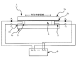
図1は、本発明のEC装置の一実施態様を示す断面模式図である。図1において、基板1a,1bには、それぞれ電極2a,2bが形成されている。基板1a,1bはギャップ制御粒子(不図示)を含むシール3を介して貼り合わされ、一対の電極2a,2b間には、少なくとも一種類のEC材料と溶媒を含むEC層4を有する。また、電極2a,2bには、それぞれ少なくとも一対の給電端子A1,A2,…,An−1,An(アノード)とC1,C2,…,Cn−1,Cn(カソード)が設置されている(nは2以上の整数)。そして、それぞれの給電端子は有効光線領域外の電極上に形成された低抵抗配線5と接続され、少なくとも一対の給電部を形成している。給電端子A1,A2,…,An−1,AnとC1,C2,…,Cn−1,Cnはそれぞれ駆動回路基板を含む駆動手段6に接続され、これらの端子間に電圧パルスが印加されることによって素子の駆動が行われる。
≪Electrochromic (EC) equipment≫
FIG. 1 is a schematic cross-sectional view showing an embodiment of the EC device of the present invention. In FIG. 1,
<基板1>
基板1a,1bとしてはガラス基板が好ましい。ガラス基板としては、光学ガラス、石英ガラス、白板ガラス、青板ガラス、ホウケイ酸ガラス、無アルカリガラス、化学強化ガラス等を用いることができ、特に透明性や耐久性、耐熱性の点から無アルカリガラスを好適に使用することができる。基板1a,1bには、電極2a,2bのほかに、基板表面、基板−電極界面及び電極−EC層界面の反射を低減して素子透過率を向上する、不図示の反射防止層やインデックスマッチング層を好適に形成することができる。
<Substrate 1>
As the
<電極2>
電極2a,2bとしては透明電極が好ましい。透明電極としては、いわゆる透明導電性酸化物であるスズドープ酸化インジウム(ITO)、酸化亜鉛、ガリウムドープ酸化亜鉛(GZO)、アルミニウムドープ酸化亜鉛(AZO)、酸化スズ、アンチモンドープ酸化スズ(ATO)、フッ素ドープ酸化スズ(FTO)、ニオビウムドープ酸化チタン(TNO)等を用いることができる。
<Electrode 2>
Transparent electrodes are preferable as the
<シール3>
シール3としては、熱硬化性樹脂や紫外線硬化性樹脂を用いることができることができるが、EC層の形成法、すなわち素子プロセスによって適宜好適な材料が選択される。また、シール3には一対の基板間隔を規定するセルギャップ制御粒子を混練しておくのが好ましい。
<Seal 3>
As the
<EC層4>
EC層4は、少なくとも一種類のEC材料と、溶媒と、を含み、さらに支持電解質や増粘剤等他の有益剤を有してもよい。
<
The
EC材料としては、酸化還元により可視光透過率が変化する化合物を好適に使用することができ、中でもチオフェン類化合物、フェナジン類化合物、ビピリジニウム塩類化合物等の有機化合物を好適に用いることができる。 As the EC material, a compound whose visible light transmittance is changed by oxidation-reduction can be preferably used. Among them, an organic compound such as a thiophene compound, a phenazine compound, or a bipyridinium salt compound can be preferably used.
溶媒としては、EC材料や支持電解質等の有益剤を溶解するものであれば特に限定されないが、極性が大きいものを好ましく用いることができる。具体的には、水や、メタノール、エタノール、プロピレンカーボネート、エチレンカーボネート、ジメチルスルホキシド、ジメトキシエタン、γ−ブチロラクトン、γ−バレロラクトン、スルホラン、ジメチルホルムアミド、ジメトキシエタン、テトラヒドロフラン、アセトニトリル、プロピオンニトリル、ベンゾニトリル、ジメチルアセトアミド、メチルピロリジノン、ジオキソラン等の有機極性溶媒が挙げられる。 The solvent is not particularly limited as long as it can dissolve a beneficial agent such as an EC material or a supporting electrolyte, but a solvent having a large polarity can be preferably used. Specifically, water, methanol, ethanol, propylene carbonate, ethylene carbonate, dimethyl sulfoxide, dimethoxyethane, γ-butyrolactone, γ-valerolactone, sulfolane, dimethylformamide, dimethoxyethane, tetrahydrofuran, acetonitrile, propiononitrile, benzonitrile. Organic polar solvents such as dimethylacetamide, methylpyrrolidinone, and dioxolane.
支持電解質としては、イオン解離性の塩であり、かつ溶媒に対して良好な溶解性を示すものであれば限定されないが、電子供与性を有する電解質を好ましく用いることができる。例えば、各種のアルカリ金属塩、アルカリ土類金属塩などの無機イオン塩や4級アンモニウム塩や環状4級アンモニウム塩などがあげられる。具体的にはLiClO4、LiSCN、LiBF4、LiAsF6、LiCF3SO3、LiPF6、LiI、NaI、NaSCN、NaClO4、NaBF4、NaAsF6、KSCN、KCl等のLi、Na、Kのアルカリ金属塩等や、(CH3)4NBF4、(C2H5)4NBF4、(n−C4H9)4NBF4、(n−C4H9)4NPF6、(C2H5)4NBr、(C2H5)4NClO4、(n−C4H9)4NClO4等の4級アンモニウム塩および環状4級アンモニウム塩等が挙げられる。
The supporting electrolyte is not limited as long as it is an ion dissociable salt and exhibits good solubility in a solvent, but an electrolyte having an electron donating property can be preferably used. Examples thereof include inorganic ion salts such as various alkali metal salts and alkaline earth metal salts, quaternary ammonium salts, and cyclic quaternary ammonium salts. Specifically, LiClO 4, LiSCN, LiBF 4,
増粘剤としては、例えばシアノエチルポリビニルアルコール、シアノエチルプルラン、及びシアノエチルセルロースから選ばれる少なくとも1種を好適に使用することができる。これらは、CR−V(シアノエチルポリビニルアルコール:軟化温度20〜40℃、誘電率18.9)、CR−S(シアノエチルプルラン:軟化温度90〜100℃、誘電率18.9)、CR−C(シアノエチルセルロース:軟化温度200℃以上、誘電率16)、CR−M(シアノエチルプルランとシアノエチルポリビニルアルコールの混合物:軟化温度40〜70℃、誘電率18.9)として、信越化学工業製から入手することが可能であり、広い温度範囲にわたる高粘性と高イオン導電性という、相反する課題を良好なバランスで解決する添加剤である。 As the thickener, for example, at least one selected from cyanoethyl polyvinyl alcohol, cyanoethyl pullulan, and cyanoethyl cellulose can be suitably used. These are CR-V (cyanoethyl polyvinyl alcohol: softening temperature 20-40 ° C., dielectric constant 18.9), CR-S (cyanoethyl pullulan: softening temperature 90-100 ° C., dielectric constant 18.9), CR-C ( Obtained from Shin-Etsu Chemical Co., Ltd. as cyanoethyl cellulose: softening temperature 200 ° C. or higher, dielectric constant 16), CR-M (mixture of cyanoethyl pullulan and cyanoethyl polyvinyl alcohol: softening temperature 40-70 ° C., dielectric constant 18.9) It is an additive that solves the conflicting problems of high viscosity and high ionic conductivity over a wide temperature range with a good balance.
EC層4の形成方法としては、基板に一対の孔を形成してEC媒体を充填する方法、シール3パターンによって形成した素子側面の充填孔からからEC媒体を真空注入する方法、基板貼り合わせと同時に真空中でEC媒体を充填する方法等が挙げられる。
The
<給電部>
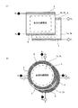
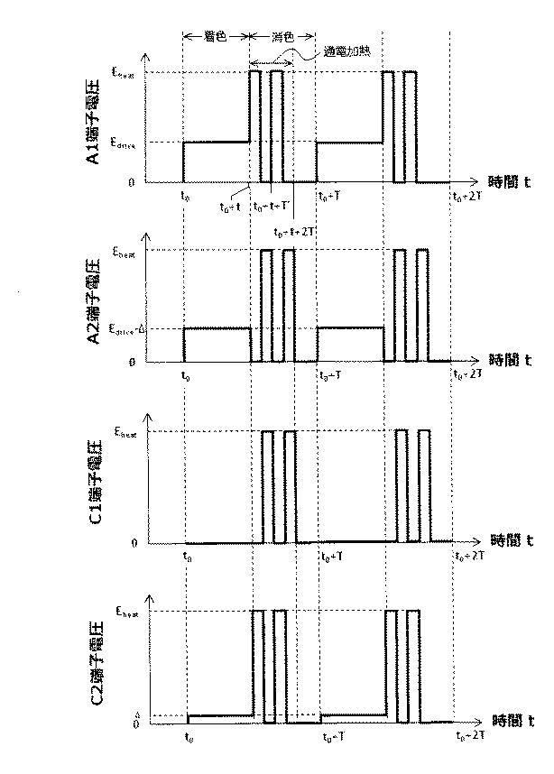
電極2a,2bのそれぞれは、第一の給電部と、第一の給電部に対向して配置された第二の給電部とからなる一対の給電部を、少なくとも一対有する。給電部は、給電端子と低抵抗配線5を有することが好ましい。図2は、本発明のEC素子の給電部の配置の一例を模式的に示す図であり、基板貼り合せ方向から見た図である。
<Power supply unit>
Each of the
先ず、図2(a)を用いて、電極及び素子外形が略四角形状であるときの低抵抗配線5の設置位置数について説明する。撮像素子は長方形形状であるので、撮像素子への入射光量を制御するEC素子は撮像素子と同じく長方形形状にするのが好適である。このとき長方形の縦横何れかの辺に給電部を設けて素子に通電を行うが、素子着消色動作を行う通常駆動時における有効光線領域内での電位分布をできるだけ小さくすることが好ましい。そのために、長辺に沿って低抵抗配線5を形成し、これに給電端子を設置して短手方向に電流を流すのが好ましい。これは通常駆動時に限らず、電極への通電によりEC層を加熱する加熱駆動の際にも同様である。つまり、短手方向の電極抵抗は長手方向の電極抵抗より必ず小さくなるために同じ電力で加熱する場合には、より低い電圧印加することが可能になるためである。したがって、図2(a)のように給電端子及び低抵抗配線5を設置して、A1とA2間及びC1とC2間で短手方向に電流を流すのが好適と言える。なお、略四角形状とは、角が丸くなっているがおおよそ四角形とみなせるものを含む。
First, with reference to FIG. 2A, the number of installation positions of the
次に図2(b)を用いて、電極及び素子外形が略円形状であるときの低抵抗配線5の設置位置、給電端子数について説明する。EC素子が略円形状であるとき、円外周に沿って2(N+1)個(N=0、1、2、…)に分割した低抵抗配線5を設置することが可能である。分割数は素子サイズや、溶液抵抗/電極抵抗比等を考慮して最適なものが選択される。図のように低抵抗配線5を4つに分割して形成した場合、電極2bにはA1、A2、A3、A4端子が接続され(すべてアノード)、電極2aにはC1、C2、C3、C4端子が接続される(すべてカソード)。なお、略円形状とは、長軸と短軸との差が小さい楕円などおおよそ円形とみなせるものを含む。
Next, with reference to FIG. 2B, the installation position of the
通常駆動時における低抵抗配線5の長手方向の電位降下を10mV程度に抑えるためには、低抵抗配線5のシート抵抗は電極のシート抵抗の1/100未満、さらに好ましくは1/500未満であることが好ましい。低抵抗配線5としては、真空成膜によって形成した薄膜銀配線や、スクリーン印刷やインクジェット塗布等によって形成した厚膜銀配線を好適に使用することができる。
In order to suppress the potential drop in the longitudinal direction of the
<駆動方法>
本発明では、一対の給電部間に、一対の電極の対向する位置に関して同位相の交番電圧を印加してEC層を加熱する加熱駆動を行う。加熱駆動は、電圧変調駆動であることが好ましい。また、加熱駆動を行うタイミングは特に限定されないが、通常駆動の前、通常駆動の休止時間、またはEC素子の温度を検知する温度検知手段により検知した温度が所定値以下の時に行うことが好ましい。
<Driving method>
In the present invention, a heating drive is performed in which an alternating voltage having the same phase is applied between a pair of power feeding portions to a position where the pair of electrodes are opposed to heat the EC layer. The heating drive is preferably voltage modulation drive. The timing for performing the heating drive is not particularly limited, but it is preferably performed when the temperature detected by the temperature detection means for detecting the temperature of the EC element before the normal drive, the pause time of the normal drive, or the EC element is not more than a predetermined value.
図3は、図2(a)のEC素子について、通常駆動の前等の通常駆動を行っていない期間(非着色動作中)に加熱駆動を行う場合の電圧波形(端子間電圧)の例である。以下、A1とA2間及びC1とC2間に印加する電圧波形としては、一対の電極の対向する位置に関して同位相の交番電圧とするのが好適であることについて説明する。 FIG. 3 is an example of a voltage waveform (inter-terminal voltage) in the case where the EC element of FIG. 2A is heated and driven during a period in which normal driving is not performed (during non-coloring operation) such as before normal driving. is there. Hereinafter, it will be described that the voltage waveform applied between A1 and A2 and between C1 and C2 is preferably an alternating voltage having the same phase with respect to the position where the pair of electrodes face each other.
先ず、一方の電極にEC層を加熱し得る電圧印加を行うことを考える。例えば、A1端子に+3V、A2端子に0Vを印加する場合、端子間電位差は通常駆動時の着色駆動電圧よりも大きな電位差が印加されるため、電極面内でアノード材料とカソード材料が分かれて着色する。すなわち、高電位のA1端子側ではアノード材料が着色し、低電位のA2端子側ではカソード材料が着色する。このとき通常駆動時の着色駆動電圧以上の高電圧が印加されるため、EC分子は高次酸化及び高次還元されてより不安定な状態となり、特に長時間行う場合は材料の劣化が懸念される。そこで、波高値及びパルス幅が同じ正電圧パルスと逆電圧パルスを短時間且つ交互に印加することで、自己消色反応を利用しながら不安定な化学種として存在する時間を、素子が着色しないという意味において実質上ゼロにすることが可能となる。 First, consider applying a voltage that can heat the EC layer to one of the electrodes. For example, when + 3V is applied to the A1 terminal and 0V is applied to the A2 terminal, the potential difference between the terminals is larger than the coloring driving voltage during normal driving, so the anode material and the cathode material are colored separately in the electrode plane. To do. That is, the anode material is colored on the high potential A1 terminal side, and the cathode material is colored on the low potential A2 terminal side. At this time, since a high voltage equal to or higher than the coloring driving voltage during normal driving is applied, EC molecules are subjected to higher-order oxidation and higher-order reduction to become more unstable. The Therefore, by applying a positive voltage pulse and a reverse voltage pulse with the same peak value and pulse width for a short time and alternately, the device does not color the time that exists as an unstable chemical species while utilizing the self-decoloring reaction. In this sense, it can be substantially zero.
次に、一対の電極両方にEC層を加熱し得る電圧印加を行うことを考える。ここで注意すべきことは、電極面内の任意の点について、電極間電位差が着色駆動電圧程度になると着色が生じてしまい、したがって通常駆動と加熱駆動を独立に行うことができなくなるということである。そこで、A1とA2間及びC1とC2間に印加する電圧波形は、一対の電極の対向する位置に関して同位相の交番電圧とするのが好適であると言えるのである。 Next, consider applying a voltage that can heat the EC layer to both of the pair of electrodes. What should be noted here is that coloring occurs at any point in the electrode surface when the interelectrode potential difference is about the coloring driving voltage, and therefore normal driving and heating driving cannot be performed independently. is there. Therefore, it can be said that the voltage waveform applied between A1 and A2 and between C1 and C2 is preferably an alternating voltage having the same phase with respect to the position where the pair of electrodes face each other.
電極の抵抗値によっても異なるが、加熱駆動に適用する電圧波高値は1Vから10V程度が好適で、パルス幅は100ms以下、より好ましくは100μs以下である。 Although it depends on the resistance value of the electrode, the voltage peak value applied to the heating drive is preferably about 1 V to 10 V, and the pulse width is 100 ms or less, more preferably 100 μs or less.
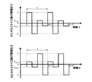
図4は、図2(b)のEC素子について、非着色動作中に加熱駆動を行う場合の電圧波形(端子間電圧)の例を示した図である。 FIG. 4 is a diagram illustrating an example of a voltage waveform (inter-terminal voltage) when the EC element of FIG. 2B is heated and driven during a non-coloring operation.
図4に示すように、A1−A3間およびC3−C1間、さらにA2−A4間およびC4−C2間には、前述した通り図3のように一対の電極の対向する位置に関して同位相の交番電圧を印加するのが好ましい。ただし、Eopenは開放電圧で、今の場合は略零である。EC層を均一に加熱することを考えると、2系統の電圧印加は図4に示した通り交互に同一時間行うことが好ましい。すなわち、一対の給電部をN+1組有する場合(Nは1以上の整数)、一対の給電部間のそれぞれに、位相が2π/(N+1)ラジアンずつずれた同一形状の電圧パルスを印加することが好ましい。 As shown in FIG. 4, between A1 and A3 and between C3 and C1, and further between A2 and A4 and between C4 and C2, as described above, as shown in FIG. It is preferable to apply a voltage. However, Eopen is an open circuit voltage, which is substantially zero in this case. Considering uniform heating of the EC layer, it is preferable to apply the two systems of voltage alternately for the same time as shown in FIG. That is, when there are N + 1 pairs of power supply units (N is an integer equal to or greater than 1), voltage pulses having the same shape with phases shifted by 2π / (N + 1) radians can be applied between the pair of power supply units. preferable.
次に、図2(a)のEC素子について、通常駆動中に加熱駆動を行う場合の各端子に印加する電圧波形について図5を用いて説明する。 Next, voltage waveforms applied to each terminal in the case where the EC element shown in FIG. 2A is heated during normal driving will be described with reference to FIG.
通常駆動は電圧波高値Edrive、周期T固定のパルス幅変調駆動(0≦t≦T)により、任意の光学濃度(0≦ΔOD≦ΔODmax)に設定することが可能である。このとき一周期当たりの休止時間(非着色時間)はT−tであり、この休止時間内において加熱駆動を行うことが可能である。従って、一周期当たりに加熱駆動を行うことができる時間は設定する光学濃度に依存することになる。しかし、EC材料の濃度を大きくすれば最大光学濃度を十分大きくとれること、加熱電圧を約10V程度までの間で設定できること等を考慮すれば、加熱駆動は通常駆動と略独立に制御を行うことが可能となる。従って、通常駆動は光学濃度設定に休止時間を利用するものであればどのようなものでもよい。具体的には、一対の電極に設置された各2個の給電端子のうち、それぞれ1つ(A1端子とC1端子)を選択して図5に示したような駆動を行っても良いし、更にA2端子とC2端子を選択してこれらの間で交番駆動を行っても良い。 The normal driving can be set to an arbitrary optical density (0 ≦ ΔOD ≦ ΔOD max ) by the voltage peak value E drive and the pulse width modulation driving (0 ≦ t ≦ T) with a fixed period T. At this time, the rest time (non-coloring time) per cycle is Tt, and heating driving can be performed within this rest time. Accordingly, the time during which heating driving can be performed per cycle depends on the optical density to be set. However, considering that the maximum optical density can be sufficiently increased by increasing the concentration of the EC material and that the heating voltage can be set between about 10 V, the heating drive should be controlled almost independently of the normal drive. Is possible. Accordingly, the normal drive may be any drive that uses a pause time for optical density setting. Specifically, one of each of the two power supply terminals installed on the pair of electrodes (A1 terminal and C1 terminal) may be selected and the drive shown in FIG. 5 may be performed. Further, the A2 terminal and the C2 terminal may be selected and alternate driving may be performed between them.
休止時間(非着色時間)に行う加熱駆動は周期T’固定で電圧波高値を可変とする電圧駆動を行うのが好適である。通常駆動の駆動周波数は10kHz程度であるので、加熱駆動の駆動周波数はその10倍程度、つまり100kHz以上(周期は10μs以下)とするのが温度制御上好ましいと言える。 It is preferable that the heating driving performed during the downtime (non-coloring time) is voltage driving in which the voltage peak value is variable with the period T ′ fixed. Since the driving frequency for normal driving is about 10 kHz, it can be said that the driving frequency for heating driving is preferably about 10 times that is, that is, 100 kHz or more (the cycle is 10 μs or less) in terms of temperature control.
図5においては、休止時間T−tの内2T’分の加熱駆動を行った例であるが、加熱電圧を下げて休止時間にわたって加熱駆動を行うことによっても同様の効果を得ることも可能である。 FIG. 5 shows an example in which the heating drive for 2T ′ of the rest time Tt is performed, but the same effect can be obtained by lowering the heating voltage and performing the heat drive over the rest time. is there.
≪EC素子の用途等≫
<光学フィルタ>
本発明に係る光学フィルタは、本発明に係るEC装置と、このEC装置が有するEC素子に接続されている能動素子とを有する。能動素子は、EC素子を駆動し、EC素子を通過する光の光量を調整するものである。能動素子は、例えば、増幅素子、スイッチング素子が挙げられ、より具体的にはトランジスタ、MIM素子が挙げられる。
≪Use of EC element≫
<Optical filter>
The optical filter according to the present invention includes the EC device according to the present invention and an active element connected to an EC element included in the EC device. The active element drives the EC element and adjusts the amount of light passing through the EC element. Examples of the active element include an amplifying element and a switching element, and more specifically, a transistor and an MIM element.
<レンズユニット>
本発明に係るレンズユニットは、本発明に係る光学フィルタと、撮像光学系とを有する。光学フィルタにより撮像光学系を通過する光、または通過した光の光量を調整することができる。撮像光学系は複数のレンズ要素を有するレンズ群である。レンズユニットが有する光学フィルタは、レンズとレンズとの間に有していてもよく、レンズユニットの外部に取り付けられてもよい。
<Lens unit>
The lens unit according to the present invention includes the optical filter according to the present invention and an imaging optical system. The light that passes through the imaging optical system or the amount of light that has passed through the optical filter can be adjusted. The imaging optical system is a lens group having a plurality of lens elements. The optical filter included in the lens unit may be provided between the lenses, or may be attached to the outside of the lens unit.
<撮像装置>
本発明に係る撮像装置は、本発明に係る光学フィルタと、光学フィルタを透過した光を受光する撮像素子とを有する。本発明に係る光学フィルタをカメラ等の撮像装置に用いた場合、撮像素子のゲインを下げることなく、光量を低減することができる。
<Imaging device>
An imaging device according to the present invention includes the optical filter according to the present invention and an imaging element that receives light transmitted through the optical filter. When the optical filter according to the present invention is used in an imaging apparatus such as a camera, the amount of light can be reduced without reducing the gain of the imaging element.
図6は、本発明の撮像装置を示す模式図であり、図6(a)は、本発明の光学フィルタを用いたレンズユニットを有する撮像装置、図6(b)は、本発明の光学フィルタを有する撮像装置である。図6に示す様に、レンズユニット102はマウント部材(不図示)を介して撮像ユニット103に着脱可能に接続されている。
FIG. 6 is a schematic diagram showing an imaging device of the present invention, FIG. 6A is an imaging device having a lens unit using the optical filter of the present invention, and FIG. 6B is an optical filter of the present invention. It is an imaging device which has. As shown in FIG. 6, the
レンズユニット102は、複数のレンズあるいはレンズ群を有するユニットである。例えば、図6(a)において、レンズユニット102は、絞りより後でフォーカシングを行うリアフォーカス式のズームレンズを表している。被写体側(紙面向かって左側)より順に正の屈折力の第1のレンズ群104、負の屈折力の第2のレンズ群105、正の屈折力の第3のレンズ群106、正の屈折力の第4のレンズ群107の4つのレンズ群を有する。第2のレンズ群105と第3のレンズ群106の間隔を変化させて変倍を行い、第4のレンズ群107の一部のレンズ群を移動させてフォーカスを行う。レンズユニット102は、例えば、第2のレンズ群105と第3のレンズ群106の間に開口絞り108を有し、また、第3のレンズ群106と第4のレンズ群107の間に光学フィルタ101を有する。レンズユニット102を通過する光は、各レンズ群102乃至107、開口絞り108および光学フィルタ101を通過するよう配置されており、開口絞り108および光学フィルタ101を用いて光量の調整を行うことができる。
The
また、レンズユニット102内の構成は適宜変更可能である。例えば、光学フィルタ101は開口絞り108の前(被写体側)あるいは後(撮像ユニット103側)に配置でき、また、第1のレンズ群104よりも前に配置しても良く、第4のレンズ群107よりも後に配置しても良い。光の収束する位置に配置すれば、光学フィルタ101の面積を小さくできるなどの利点がある。また、レンズユニット102の形態も適宜選択可能であり、リアフォーカス式の他、絞りより前でフォーカシングを行うインナーフォーカス式であっても良く、その他の方式であっても構わない。また、ズームレンズ以外にも魚眼レンズやマクロレンズなどの特殊レンズも適宜選択可能である。
Further, the configuration in the
撮像ユニット103が有するガラスブロック109は、ローパスフィルタやフェースプレートや色フィルタ等のガラスブロックである。また、撮像素子110は、レンズユニット102を通過した光を受光するセンサ部であって、CCDやCMOS等が使用できる。また、フォトダイオードのような光センサであっても良く、光の強度あるいは波長の情報を取得し出力するものを適宜利用可能である。
The
図6(a)のように、光学フィルタ101がレンズユニット102に組み込まれている場合、駆動手段はレンズユニット102内に配置されても良く、例えば撮像ユニット103内等、レンズユニット102外に配置されても良い。レンズユニット102外に配置される場合は、配線を通してレンズユニット102内外のEC素子と駆動手段を接続し、駆動制御する。
As shown in FIG. 6A, when the
図6(b)に示す様に、撮像ユニット103が本発明の光学フィルタ101を有していても良い。光学フィルタ101は撮像ユニット103内部の適当な箇所に配置され、撮像素子110は光学フィルタ101を通過した光を受光するよう配置されていれば良い。図6(b)においては、例えば光学フィルタ101は撮像素子110の直前に配置されている。撮像ユニット103が光学フィルタ101を内蔵する場合、接続されるレンズユニット102自体が光学フィルタ101を持たなくても良いため、既存のレンズユニットを用いた調光可能な撮像装置を構成することが可能となる。
As shown in FIG. 6B, the
このような撮像装置は、光量調整と撮像素子の組合せを有する製品に適用可能である。例えばカメラ、デジタルカメラ、ビデオカメラ、デジタルビデオカメラに使用可能であり、また、携帯電話やスマートフォン、PC、タブレットなど撮像装置を内蔵する製品にも適用できる。 Such an image pickup apparatus can be applied to a product having a combination of light amount adjustment and an image pickup element. For example, it can be used for a camera, a digital camera, a video camera, a digital video camera, and can also be applied to a product incorporating an imaging device such as a mobile phone, a smartphone, a PC, or a tablet.
本発明の光学フィルタを調光部材として用いることで、調光量を一つのフィルタで適宜可変させることが可能となり、部材点数の削減や省スペース化といった利点がある。 By using the optical filter of the present invention as a dimming member, the dimming amount can be appropriately changed by a single filter, and there are advantages such as reduction in the number of members and space saving.
<窓材>
本発明の窓材は、本発明のEC装置と、このEC装置が有するEC素子に接続されている能動素子とを有する。能動素子は、EC素子を駆動し、EC素子を通過する光の光量を調整するものである。能動素子は、例えば、増幅素子、スイッチング素子が挙げられ、より具体的にはトランジスタ、MIM素子が挙げられる。
<Window material>
The window material of the present invention includes the EC device of the present invention and an active element connected to the EC element of the EC device. The active element drives the EC element and adjusts the amount of light passing through the EC element. Examples of the active element include an amplifying element and a switching element, and more specifically, a transistor and an MIM element.
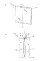
図7は、本発明の窓材を示す図であり、図7(a)は斜視図、図7(b)は図7(a)のX−X’断面図である。図7の窓材111は調光窓であり、EC素子7と、それを挟持する透明板113と、全体を囲繞して一体化するフレーム112とから成る。駆動手段はフレーム112内に一体化されていても良く、フレーム112外に配置され配線を通してEC素子7と接続されていても良い。
7A and 7B are views showing the window material of the present invention, in which FIG. 7A is a perspective view and FIG. 7B is a cross-sectional view taken along line X-X ′ of FIG. A
透明板113は光透過率が高い材料であれば特に限定されず、窓としての利用を考慮すればガラス素材であることが好ましい。図7において、EC素子7は透明板113と独立した構成部材であるが、例えば、EC素子7の基板1を透明板113と見なしても構わない。
The
フレーム112は材質を問わないが、EC素子7の少なくとも一部を被覆し、一体化された形態を有するもの全般をフレームとして見なして構わない。
The
係る調光窓は、例えば日中の太陽光の室内への入射量を調整する用途に適用できる。太陽の光量の他、熱量の調整にも適用できるため、室内の明るさや温度の制御に使用することが可能である。また、シャッターとして、室外から室内への眺望を遮断する用途にも適用可能である。このような調光窓は、建造物用のガラス窓の他に、自動車や電車、飛行機、船など乗り物の窓、時計や携帯電話の表示面のフィルタにも適用可能である。 Such a light control window can be applied to, for example, an application for adjusting the amount of sunlight entering the room during the daytime. Since it can be applied to the adjustment of the amount of heat in addition to the amount of sunlight, it can be used to control the brightness and temperature of the room. In addition, the present invention can also be applied as a shutter for blocking the view from the outside to the room. Such a light control window can be applied to a window of a vehicle such as an automobile, a train, an airplane, a ship, a filter of a display surface of a clock or a mobile phone, in addition to a glass window for a building.
以下、本発明のEC装置の実施例について説明する。 Embodiments of the EC apparatus according to the present invention will be described below.
<実施例1>
図1及び図2(a)に示すEC素子を作成した。基板1a,1bとして、厚さ0.7mmのガラス基板(Corning社製EAGLE−XG)を用いた。基板上に、電極2a,2bとして、シート抵抗10Ω/□のITO透明電極を形成し、これを一対の透明電極基板として使用した。
<Example 1>
The EC element shown in FIGS. 1 and 2A was produced. As the
本実施例のEC素子は基板面に対して垂直方向の素子外形が長方形であるため、素子長辺に沿って一対の低抵抗配線5を有効光線領域外に形成した。低抵抗配線5は銀ナノ粒子ペーストを使用したスクリーン印刷によって、シート抵抗6.6mΩ/□(膜厚5μm)の銀厚膜を形成した。このとき低抵抗配線5と電極2a,2bのシート抵抗比は1/1000以下であった。
Since the EC device according to this example has a rectangular device outer shape in the direction perpendicular to the substrate surface, a pair of
ギャップ制御粒子(積水化学工業社製ミクロパール−SP(直径30μm))と熱硬化型エポキシ樹脂(三井化学製ストラクトボンドHC−1850)を混練した。この混練物を用い、一方の透明電極基板に、ディスペンサ装置を使用してEC媒体注入用の開口部があるシールパターンを描画塗布し、もう一方の透明電極基板と貼り合わせて電極間間隙30μmの素子を作製した。ここでEC媒体注入部を除く、素子の有効光線領域は11×18mmとした。
Gap control particles (Sekisui Chemical Co., Ltd. Micropearl-SP (
次に、EC媒体として、下記構造式(A)に示したアノード性EC材料A(フェナジン類化合物)と、下記構造式(B)に示したカソード性EC材料B(ビピリジニウム塩類化合物)とを炭酸プロピレン溶媒に溶解したものを作製した。このとき、アノード性EC材料Aおよびカソード性EC材料Bの濃度は100mMとした。 Next, as an EC medium, anodic EC material A (phenazine compound) represented by the following structural formula (A) and cathodic EC material B (bipyridinium salt compound) represented by the following structural formula (B) are carbonated. What was melt | dissolved in the propylene solvent was produced. At this time, the concentrations of the anodic EC material A and the cathodic EC material B were 100 mM.
先に作製した開口部を残して作製した素子に真空注入法によりEC媒体を充填し、開口部を紫外線硬化型エポキシ樹脂により封止した。さらに低抵抗配線5にはリード線をハンダ付けして、各端子に独立に電圧印加できるEC素子を作製した。
An EC medium was filled in the element prepared by leaving the opening prepared previously by a vacuum injection method, and the opening was sealed with an ultraviolet curable epoxy resin. Furthermore, a lead wire was soldered to the
[素子評価]
作製したEC素子を、電気化学特性、光学特性及び温度特性を同時に評価できる装置に設置して特性評価を行った。
[Element evaluation]
The produced EC element was installed in an apparatus capable of simultaneously evaluating electrochemical characteristics, optical characteristics, and temperature characteristics, and the characteristics were evaluated.
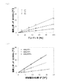
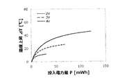
先ず、通常駆動前の非着色時において、加熱電圧の電圧波高値を変えて、加熱駆動(駆動周波数100kHz、デューティ100%)を行った時の素子の温度変化を測定した。図8に示すように、時間とともに素子温度が上昇していく様子が見て取れ、例えば4Vでは1分で温度上昇ΔTを25℃以上とすることができることが分かった。次に各電圧でデューティを変えて同様に温度上昇を確認した。図9(a)に示すように、デューティに関しては、電圧に依らず線形に温度上昇していることが分かる。また、図9(b)に示すように、電圧に関しては、デューティに依らず電圧の自乗に比例して温度上昇していることが分かる。さらに、各電圧について投入電力に対する温度上昇を見た場合、図10に示すように、投入電力が小さいときは温度上昇は印加電圧に依らないが、投入電力が大きくなると電圧が大きいほど温度上昇も大きくなり、EC層を効率良く加熱していることが分かる。
First, the temperature change of the element when heating driving (
比較のために、加熱駆動を行わない場合についても素子温度変化を確認したところ、温度上昇は1℃未満であった。 For comparison, when the element temperature change was confirmed even when the heating drive was not performed, the temperature rise was less than 1 ° C.
また、加熱駆動中において透過率変化は見られず、また加熱駆動前後における電流−電圧特性も変化が見られず、EC素子の特性劣化は生じていなかった。 Further, no change in transmittance was observed during the heating driving, and no change was observed in the current-voltage characteristics before and after the heating driving, and the EC element characteristics did not deteriorate.
<実施例2>
低抵抗配線5を、スパッタリングによって、シート抵抗16mΩ/□(膜厚1.2μm)の銀薄膜として形成した以外は、実施例1と同様にしてEC素子を作成した。但し、銀薄膜の密着性を向上する目的で下引き層として膜厚50nmのチタン薄膜を形成している。銀配線とITO電極のシート抵抗比は1/625であった。
<Example 2>
An EC element was prepared in the same manner as in Example 1 except that the
[素子評価]
作製したEC素子を、実施例1と同様の装置に設置し、装置ごと恒温槽に投入して特性評価を行った。
[Element evaluation]
The produced EC element was installed in the same apparatus as in Example 1, and the entire apparatus was put into a thermostatic chamber to evaluate the characteristics.
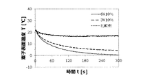
先ず恒温槽の温度を−5℃に設定して素子温度が十分安定した後、非着色状態で加熱駆動(電圧3V、駆動周波数100kHz、デューティ100%)を行い、素子温度を約20℃まで上昇させた。引き続き素子の通常駆動と加熱駆動を行った。具体的には、通常駆動は電圧0.75V、駆動周波数10kHz、デューティ90%で行い、加熱駆動は通常駆動の休止期間中、即ちデューティ10%、駆動周波数100kHzで行った。素子の光学濃度は1.8で約6段分の減光状態であった。このとき加熱電圧を6V、3Vとし、さらに比較のために加熱駆動を行わない場合についても評価を行った。加熱電圧が3Vである場合に各端子に印加した電圧を表1にまとめて示した。加熱電圧が6Vである場合は、加熱駆動の電圧3Vを6Vに変更する以外は、表1と同様である。
First, the temperature of the thermostat is set to −5 ° C. and the element temperature is sufficiently stabilized. Then, heating driving (
素子温度変化については図11に示した。加熱駆動なし(比較例)では300sで素子温度が約20℃から0.5℃まで低下しているのに対し、3Vの加熱駆動を行った場合は4.1℃、6Vの加熱駆動を行った場合は17.2℃であり、加熱駆動によって素子温度を維持できていることが分かった。また、加熱駆動なしでは素子温度低下にともなう光学濃度変化が見られたが、加熱駆動を行った場合、光学濃度変化はごく僅かであった。通常駆動と加熱駆動を300s行った後に消色を行い、各駆動条件で消色応答を確認したところ、6Vで加熱駆動を行った場合は2.2s、3Vで加熱駆動を行った場合は3.1s、加熱駆動なしでは4.0sであった。加熱駆動により応答時間が早く維持できていることがわかる。 The element temperature change is shown in FIG. Without heating drive (comparative example), the element temperature dropped from about 20 ° C to 0.5 ° C in 300 s, whereas when 3V heating drive was performed, 4.1 ° C and 6V heating drive was performed. In this case, it was 17.2 ° C., and it was found that the element temperature could be maintained by heating driving. In addition, a change in optical density with a decrease in element temperature was observed without heating driving, but a change in optical density was negligible when heating driving was performed. After performing normal driving and heating driving for 300 s, erasing was performed, and the decoloring response was confirmed under each driving condition. When heating driving was performed at 6 V, 2.2 s was used and when heating driving was performed at 3 V, 3 was performed. 0.1 s, 4.0 s without heating drive. It can be seen that the response time can be quickly maintained by the heating drive.
さらに、本実施例においても、素子温度変化にともなう光学濃度変化以外の着色異常や、加熱駆動前後における電流−電圧特性変化は見られず、EC素子の特性劣化は生じていなかった。 Further, also in this example, there was no coloring abnormality other than the optical density change accompanying the change in the element temperature, and no change in the current-voltage characteristic before and after the heating drive, and the characteristic deterioration of the EC element did not occur.
1a,1b:基板、2a,2b:電極、3:シール、4:EC層、5:低抵抗配線、6:駆動手段、7:EC素子 1a, 1b: substrate, 2a, 2b: electrode, 3: seal, 4: EC layer, 5: low resistance wiring, 6: driving means, 7: EC element
Claims (24)
前記エレクトロクロミック層は、少なくとも一種のエレクトロクロミック材料と、溶媒とを含み、
前記一対の電極のそれぞれは、第一の給電部と、前記第一の給電部に対向して配置された第二の給電部とからなる一対の給電部を有し、
前記駆動手段は、前記一対の給電部間に、前記一対の電極の対向する位置に関して同位相の交番電圧を印加して前記エレクトロクロミック層を加熱する加熱駆動を行うことを特徴とするエレクトロクロミック装置。 An electrochromic device having a pair of electrodes, an electrochromic element having an electrochromic layer disposed between the pair of electrodes, and a driving means for driving the electrochromic element,
The electrochromic layer includes at least one electrochromic material and a solvent,
Each of the pair of electrodes has a pair of power feeding units including a first power feeding unit and a second power feeding unit disposed to face the first power feeding unit,
The electrochromic device is characterized in that the driving means performs heating driving that heats the electrochromic layer by applying an alternating voltage having the same phase between the pair of power feeding portions with respect to positions where the pair of electrodes are opposed to each other. .
前記一対の給電部間に、前記一対の電極の対向する位置に関して同位相の交番電圧を印加して前記エレクトロクロミック層を加熱する加熱駆動を行うことを特徴とするエレクトロクロミック素子の駆動方法。 A pair of electrodes, and an electrochromic layer that is disposed between the pair of electrodes and includes at least one electrochromic material and a solvent, and each of the pair of electrodes includes a first power feeding unit and the electrochromic layer. A method for driving an electrochromic element having a pair of power feeding portions composed of a second power feeding portion arranged to face the first power feeding portion,
A driving method of an electrochromic element, wherein an alternating voltage having the same phase is applied between the pair of power feeding portions at a position where the pair of electrodes are opposed to heat the electrochromic layer.
Priority Applications (3)
| Application Number | Priority Date | Filing Date | Title |
|---|---|---|---|
| JP2017055343A JP2018159727A (en) | 2017-03-22 | 2017-03-22 | Electrochromic device and method for driving electrochromic device |
| US15/920,687 US10437127B2 (en) | 2017-03-22 | 2018-03-14 | Electrochromic apparatus and method of driving electrochromic device, as well as optical filter, lens unit, imaging apparatus and window member |
| KR1020180032397A KR20180107742A (en) | 2017-03-22 | 2018-03-21 | Electrochromic apparatus and method of driving electrochromic device, as well as optical filter, lens unit, imaging apparatus and window member |
Applications Claiming Priority (1)
| Application Number | Priority Date | Filing Date | Title |
|---|---|---|---|
| JP2017055343A JP2018159727A (en) | 2017-03-22 | 2017-03-22 | Electrochromic device and method for driving electrochromic device |
Publications (1)
| Publication Number | Publication Date |
|---|---|
| JP2018159727A true JP2018159727A (en) | 2018-10-11 |
Family
ID=63582443
Family Applications (1)
| Application Number | Title | Priority Date | Filing Date |
|---|---|---|---|
| JP2017055343A Pending JP2018159727A (en) | 2017-03-22 | 2017-03-22 | Electrochromic device and method for driving electrochromic device |
Country Status (3)
| Country | Link |
|---|---|
| US (1) | US10437127B2 (en) |
| JP (1) | JP2018159727A (en) |
| KR (1) | KR20180107742A (en) |
Cited By (3)
| Publication number | Priority date | Publication date | Assignee | Title |
|---|---|---|---|---|
| US20200292906A1 (en) * | 2019-03-15 | 2020-09-17 | Canon Kabushiki Kaisha | Electrochromic element |
| WO2022075017A1 (en) * | 2020-10-05 | 2022-04-14 | ソニーグループ株式会社 | Light control device, image display device, and display device |
| CN115202120A (en) * | 2022-08-02 | 2022-10-18 | 中国科学院苏州纳米技术与纳米仿生研究所 | Electrochromic assembly and manufacturing method thereof |
Families Citing this family (2)
| Publication number | Priority date | Publication date | Assignee | Title |
|---|---|---|---|---|
| EP3803017B1 (en) * | 2018-06-07 | 2023-01-18 | Saint-Gobain Glass France | Corner joint for insulating glass with electric line |
| CN112835243B (en) * | 2019-11-22 | 2022-12-02 | 北京开阳亮微科技有限公司 | Electrochromic device |
Family Cites Families (6)
| Publication number | Priority date | Publication date | Assignee | Title |
|---|---|---|---|---|
| JPS61245143A (en) | 1985-04-23 | 1986-10-31 | Asahi Glass Co Ltd | Dimmer |
| JP5697377B2 (en) * | 2010-08-20 | 2015-04-08 | キヤノン株式会社 | Electrochromic light control device and imaging device |
| JP2015141203A (en) | 2014-01-27 | 2015-08-03 | キヤノン株式会社 | Electrochromic element, and imaging optical system, imaging device and window material using the same |
| US20160041447A1 (en) | 2014-08-05 | 2016-02-11 | Canon Kabushiki Kaisha | Method and apparatus for driving an electrochromic element |
| JP6727755B2 (en) | 2015-03-13 | 2020-07-22 | キヤノン株式会社 | Electrochromic device, optical filter, imaging device, lens unit and window material, and electrochromic device driving method |
| US10295821B2 (en) * | 2016-08-19 | 2019-05-21 | Oakley, Inc. | Laminated lenses with anti-fogging functionality |
-
2017
- 2017-03-22 JP JP2017055343A patent/JP2018159727A/en active Pending
-
2018
- 2018-03-14 US US15/920,687 patent/US10437127B2/en not_active Expired - Fee Related
- 2018-03-21 KR KR1020180032397A patent/KR20180107742A/en not_active Application Discontinuation
Cited By (4)
| Publication number | Priority date | Publication date | Assignee | Title |
|---|---|---|---|---|
| US20200292906A1 (en) * | 2019-03-15 | 2020-09-17 | Canon Kabushiki Kaisha | Electrochromic element |
| US11796884B2 (en) * | 2019-03-15 | 2023-10-24 | Canon Kabushiki Kaisha | Electrochromic element |
| WO2022075017A1 (en) * | 2020-10-05 | 2022-04-14 | ソニーグループ株式会社 | Light control device, image display device, and display device |
| CN115202120A (en) * | 2022-08-02 | 2022-10-18 | 中国科学院苏州纳米技术与纳米仿生研究所 | Electrochromic assembly and manufacturing method thereof |
Also Published As
| Publication number | Publication date |
|---|---|
| US20180275477A1 (en) | 2018-09-27 |
| US10437127B2 (en) | 2019-10-08 |
| KR20180107742A (en) | 2018-10-02 |
Similar Documents
| Publication | Publication Date | Title |
|---|---|---|
| CN107850814B (en) | Electrochromic element, optical filter, lens unit, imaging device, and window member | |
| JP2018159727A (en) | Electrochromic device and method for driving electrochromic device | |
| JP6504753B2 (en) | Electrochromic device, method of driving the same, optical filter, imaging device, lens unit and window material | |
| JP6727755B2 (en) | Electrochromic device, optical filter, imaging device, lens unit and window material, and electrochromic device driving method | |
| US20160306251A1 (en) | Driving device for electrochromic device, electrochromic apparatus, optical filter, imaging apparatus, lens unit, and window member including electrochromic device, and method for driving electrochromic device | |
| JP2016038583A (en) | Drive device of electrochromic element and drive method thereof | |
| JP6278384B2 (en) | OPTICAL DEVICE, IMAGING DEVICE, AND OPTICAL ELEMENT DRIVE METHOD | |
| US11194215B2 (en) | Electrochromic device, optical filter using same, lens unit, image taking device, window member, and driving method for electrochromic element | |
| JP2016206658A (en) | Electrochromic device | |
| US9946137B2 (en) | Electrochromic element, lens unit, imaging device, and window member | |
| JP6884512B2 (en) | Electrochromic elements, optical filters, lens units, imaging devices and window materials | |
| JP2018084805A (en) | Electrochromic element, optical filter using the same, lens unit, imaging apparatus, window material, and driving method of electrochromic element | |
| US20180136530A1 (en) | Electrochromic element, optical filter using the same, lens unit, imaging device, window material, and method for driving electrochromic element | |
| US11796884B2 (en) | Electrochromic element | |
| US20200033686A1 (en) | Electrochromic device and method of driving the same, lens unit, image pickup apparatus, and window member | |
| US11047171B2 (en) | Electrochromic device, and lens unit, imaging apparatus and window including the electrochromic device | |
| US20230126380A1 (en) | Electrochromic device, lens unit, imaging device, window member, and method of driving electrochromic element | |
| JP2016018189A (en) | Electrochromic device, and driving method of electrochromic element | |
| JP2020197569A (en) | Method of driving electrochromic element, electrochromic device, and image capturing device | |
| JP2019204079A (en) | Electrochromic element, imaging device using the same, transmittance variable window | |
| JP2017090601A (en) | Electrochromic device, lens unit, imaging apparatus and window material | |
| US20220260848A1 (en) | Electrochromic element, and lens unit and imaging apparatus including the same | |
| JP2020056858A (en) | Imaging apparatus | |
| JP2023016171A (en) | Electrochromic device | |
| JP2020056897A (en) | Light control device and driving method thereof, window material, and optical filter |