JP2018152183A - Method and device for manufacturing fine structure - Google Patents
Method and device for manufacturing fine structure Download PDFInfo
- Publication number
- JP2018152183A JP2018152183A JP2017046223A JP2017046223A JP2018152183A JP 2018152183 A JP2018152183 A JP 2018152183A JP 2017046223 A JP2017046223 A JP 2017046223A JP 2017046223 A JP2017046223 A JP 2017046223A JP 2018152183 A JP2018152183 A JP 2018152183A
- Authority
- JP
- Japan
- Prior art keywords
- ion beam
- sample
- gas
- control
- manufacturing
- Prior art date
- Legal status (The legal status is an assumption and is not a legal conclusion. Google has not performed a legal analysis and makes no representation as to the accuracy of the status listed.)
- Pending
Links
Images


Classifications
-
- H—ELECTRICITY
- H01—ELECTRIC ELEMENTS
- H01J—ELECTRIC DISCHARGE TUBES OR DISCHARGE LAMPS
- H01J37/00—Discharge tubes with provision for introducing objects or material to be exposed to the discharge, e.g. for the purpose of examination or processing thereof
- H01J37/30—Electron-beam or ion-beam tubes for localised treatment of objects
- H01J37/317—Electron-beam or ion-beam tubes for localised treatment of objects for changing properties of the objects or for applying thin layers thereon, e.g. for ion implantation
-
- H—ELECTRICITY
- H01—ELECTRIC ELEMENTS
- H01J—ELECTRIC DISCHARGE TUBES OR DISCHARGE LAMPS
- H01J37/00—Discharge tubes with provision for introducing objects or material to be exposed to the discharge, e.g. for the purpose of examination or processing thereof
- H01J37/02—Details
- H01J37/04—Arrangements of electrodes and associated parts for generating or controlling the discharge, e.g. electron-optical arrangement, ion-optical arrangement
- H01J37/045—Beam blanking or chopping, i.e. arrangements for momentarily interrupting exposure to the discharge
-
- H—ELECTRICITY
- H01—ELECTRIC ELEMENTS
- H01J—ELECTRIC DISCHARGE TUBES OR DISCHARGE LAMPS
- H01J2237/00—Discharge tubes exposing object to beam, e.g. for analysis treatment, etching, imaging
- H01J2237/006—Details of gas supplies, e.g. in an ion source, to a beam line, to a specimen or to a workpiece
-
- H—ELECTRICITY
- H01—ELECTRIC ELEMENTS
- H01J—ELECTRIC DISCHARGE TUBES OR DISCHARGE LAMPS
- H01J2237/00—Discharge tubes exposing object to beam, e.g. for analysis treatment, etching, imaging
- H01J2237/30—Electron or ion beam tubes for processing objects
- H01J2237/304—Controlling tubes
- H01J2237/30472—Controlling the beam
-
- H—ELECTRICITY
- H01—ELECTRIC ELEMENTS
- H01J—ELECTRIC DISCHARGE TUBES OR DISCHARGE LAMPS
- H01J2237/00—Discharge tubes exposing object to beam, e.g. for analysis treatment, etching, imaging
- H01J2237/30—Electron or ion beam tubes for processing objects
- H01J2237/317—Processing objects on a microscale
- H01J2237/31701—Ion implantation
- H01J2237/31706—Ion implantation characterised by the area treated
- H01J2237/3171—Ion implantation characterised by the area treated patterned
- H01J2237/31713—Focused ion beam
-
- H—ELECTRICITY
- H01—ELECTRIC ELEMENTS
- H01J—ELECTRIC DISCHARGE TUBES OR DISCHARGE LAMPS
- H01J37/00—Discharge tubes with provision for introducing objects or material to be exposed to the discharge, e.g. for the purpose of examination or processing thereof
- H01J37/30—Electron-beam or ion-beam tubes for localised treatment of objects
Abstract
Description
本発明は、微細構造体の製造方法および製造装置に関し、例えばMEMS(Micro Electro Mechanical Systems)などの微細構造体を製造する微細構造体の製造方法および製造装置に関する。 The present invention relates to a manufacturing method and a manufacturing apparatus for a fine structure, and relates to a manufacturing method and a manufacturing apparatus for a fine structure for manufacturing a fine structure such as MEMS (Micro Electro Mechanical Systems).
特許文献1には、集束イオンビーム装置において、ガス種毎にブランキング電極に電圧印加するタイミングの設定値を記憶し、ガス種に対応するタイミングの設定値をブランキング電極に設定する技術が開示されている。 Patent Document 1 discloses a technique for storing a set value of timing for applying a voltage to a blanking electrode for each gas type in a focused ion beam apparatus, and setting a set value for timing corresponding to the gas type in a blanking electrode. Has been.
上述した特許文献1の技術では、ガス種毎にブランキング電極に電圧印加するタイミングを切り替えることができる。しかしながら、特許文献1の技術を用いて、ガス種毎にブランキングのタイミングを切り替えるだけでは、所望の加工位置以外にイオンビームが照射されることを回避できない。 In the technique of Patent Document 1 described above, the timing for applying a voltage to the blanking electrode can be switched for each gas type. However, by simply switching the blanking timing for each gas type using the technique of Patent Document 1, it is not possible to avoid irradiation with an ion beam other than the desired processing position.
本発明の目的は、所望の加工位置以外にイオンビームが照射されることを回避する技術を提供することにある。 The objective of this invention is providing the technique which avoids that an ion beam is irradiated other than a desired processing position.
本発明の前記ならびにその他の目的と新規な特徴については、本明細書の記述および添付図面から明らかになるであろう。 The above and other objects and novel features of the present invention will be apparent from the description of this specification and the accompanying drawings.
本願において開示される発明のうち、代表的なものの概要を簡単に説明すれば、次のとおりである。 Of the inventions disclosed in the present application, the outline of typical ones will be briefly described as follows.
一実施の形態における微細構造体の製造方法は、試料へイオンビームを照射して微細構造体を製造する微細構造体の製造方法である。微細構造体の製造方法は、試料へイオンビームを照射する工程と、試料へガスを供給する工程と、試料へのガスの供給を停止する工程と、試料へのイオンビームの照射を停止する工程と、を有する。そして、イオンビームを照射する工程はガスを供給する工程より先に行われる、もしくは、ガスの供給を停止する工程はイオンビームの照射を停止する工程より先に行われる。 A manufacturing method of a fine structure in an embodiment is a manufacturing method of a fine structure in which a fine structure is manufactured by irradiating a sample with an ion beam. A method for manufacturing a microstructure includes a step of irradiating a sample with an ion beam, a step of supplying a gas to the sample, a step of stopping supply of a gas to the sample, and a step of stopping irradiation of the ion beam to the sample And having. The step of irradiating the ion beam is performed prior to the step of supplying the gas, or the step of stopping the supply of gas is performed prior to the step of stopping the irradiation of the ion beam.
一実施の形態における微細構造体の製造装置は、試料へイオンビームを照射して微細構造体を製造する微細構造体の製造装置である。微細構造体の製造装置は、試料へイオンビームを照射する制御と、試料へガスを供給する制御と、試料へのガスの供給を停止する制御と、試料へのイオンビームの照射を停止する制御と、を行う制御装置を有する。そして、制御装置において、イオンビームを照射する制御はガスを供給する制御より先に行われる、もしくは、ガスの供給を停止する制御はイオンビームの照射を停止する制御より先に行われる。 A fine structure manufacturing apparatus according to an embodiment is a fine structure manufacturing apparatus that manufactures a fine structure by irradiating a sample with an ion beam. The microstructure manufacturing apparatus includes a control for irradiating a sample with an ion beam, a control for supplying a gas to the sample, a control for stopping the supply of gas to the sample, and a control for stopping irradiation of the ion beam to the sample. And a control device for performing In the control device, the control for irradiating the ion beam is performed before the control for supplying the gas, or the control for stopping the supply of the gas is performed before the control for stopping the irradiation of the ion beam.
一実施の形態における別の微細構造体の製造方法は、試料へイオンビームを照射して微細構造体を製造する微細構造体の製造方法である。微細構造体の製造方法は、試料へイオンビームを照射する工程と、試料にイオンビームを照射することで試料を加工する工程と、試料へのイオンビームの照射を停止する工程と、を有する。そして、イオンビームを照射する工程またはイオンビームの照射を停止する工程において、イオンビームが試料上を動作する方向が複数の選択肢の中から指定される。 In another embodiment, another microstructure manufacturing method is a microstructure manufacturing method in which a sample is irradiated with an ion beam to manufacture the microstructure. The method for manufacturing a microstructure includes a step of irradiating the sample with an ion beam, a step of processing the sample by irradiating the sample with the ion beam, and a step of stopping irradiation of the ion beam to the sample. In the step of irradiating the ion beam or stopping the irradiation of the ion beam, the direction in which the ion beam operates on the sample is designated from a plurality of options.
本願において開示される発明のうち、代表的なものによって得られる効果を簡単に説明すれば以下のとおりである。 Among the inventions disclosed in the present application, effects obtained by typical ones will be briefly described as follows.
一実施の形態によれば、所望の加工位置以外にイオンビームが照射されることを回避することができる。 According to one embodiment, it is possible to avoid irradiation with an ion beam other than a desired processing position.
以下、実施の形態を図面に基づいて詳細に説明する。以下の実施の形態を説明するための全図において、同一の部材には原則として同一の符号を付し、その繰り返しの説明は省略する。なお、図面をわかりやすくするために、平面図であってもハッチングを付す場合があり、また断面図であってもハッチングを省略する場合がある。 Hereinafter, embodiments will be described in detail with reference to the drawings. In all the drawings for explaining the following embodiments, the same members are denoted by the same reference symbols in principle, and the repeated description thereof is omitted. In order to make the drawings easier to understand, even a plan view may be hatched, and even a sectional view may be omitted.
以下の実施の形態の特徴をわかりやすくするために、まず、関連技術に存在する改善の余地について説明する。 In order to make the features of the following embodiments easier to understand, first, room for improvement existing in the related art will be described.
[改善の余地]
改善の余地について、図13〜図17を用いて説明する。この改善の余地について説明する内容において、FIB(Focused Ion Beam:集束イオンビーム)加工における材料や寸法などは一例を示すものであり、本実施の形態を限定するものではない。
[Room for improvement]
The room for improvement will be described with reference to FIGS. In the description of the room for improvement, materials and dimensions in FIB (Focused Ion Beam) processing are merely examples, and the present embodiment is not limited.
例えば、MEMSなどの微細構造体の製造において、FIBの加工を用いたMEMSセンサ製造技術の開発が進んでいる。FIBの加工には、例えば、エッチング、成膜および接着などがあるが、以下においては、エッチングおよび成膜について説明する。 For example, in the manufacture of microstructures such as MEMS, development of MEMS sensor manufacturing technology using FIB processing is progressing. The processing of FIB includes, for example, etching, film formation, and adhesion. In the following, etching and film formation will be described.
まず、ブランキング動作について、図13を用いて説明する。図13は、ブランキング動作の一例を示す説明図である。一般的にFIB装置(後述する図1参照)では、図13に示すように、試料13にイオンビーム7を照射するかどうかを、ブランキング電極8に電圧を印加するかどうかで制御する。図13(a)に示すように、ブランキング電極8に電圧を印加しないブランキングOFF状態では、イオンビーム7は試料13に到達する。また、図13(b)に示すように、ブランキング電極8に電圧を印加するブランキングON状態では、イオンビーム7の経路が変化し、イオンビーム7はビーム制限アパーチャ4に遮られ、試料13に到達しない。
First, the blanking operation will be described with reference to FIG. FIG. 13 is an explanatory diagram showing an example of the blanking operation. In general, in the FIB apparatus (see FIG. 1 described later), as shown in FIG. 13, whether or not the
試料13に一定面積の加工図形の加工を行う場合のイオンビーム動作について、図14を用いて説明する。図14は、試料に一定面積の加工図形の加工を行う場合のイオンビーム動作の一例を示す説明図である。図14に示すように、試料13に一定面積の加工図形71の加工を行う場合、加工直前まではイオンビーム7はブランキング(ブランキングON)されており、加工中のみブランキングが解除される。これは、スポットビーム(集束ビーム)、プロジェクションビーム(投射ビーム)のいずれの方式を用いた場合でも共通している。
The ion beam operation in the case of processing a processed figure of a certain area on the
スポットビーム方式の場合、図14(a)に示すように、(1)加工図形71の加工始点72にイオンビーム7を照射(ブランキング解除)、(2)イオンビーム7のスキャン、(3)加工図形71の加工終点73でブランキング、の手順となる。プロジェクションビーム方式の場合、図14(b)に示すように、(1)イオンビーム7の照射(ブランキング解除)、(2)加工図形71の加工(一定時間保持)、(3)ブランキング、の手順となる。
In the case of the spot beam method, as shown in FIG. 14A, (1) the
本発明者らは、FIBで種々のパターンの加工を行う中で、ブランキングが加工形状に影響を与える場合があることを見出した。図15は、FIBで膜(例えばSiO2膜)の細線パターンを成膜した結果の上面SIM画像の一例を示す説明図である。図15に示すように、試料13上の設定エリアに細線パターン81を成膜する工程で、ブランキング動作により設定エリア以外に、この細線パターン81の上端から斜めに筋状の膜82が成膜された。この成膜された膜82の筋の方向と、ブランキング時のイオンビーム動作方向が一致することから、この筋状の膜82はブランキングのON/OFF時のイオンビーム動作で形成されたものと判明した。
The present inventors have found that blanking may affect the processing shape during processing of various patterns by FIB. FIG. 15 is an explanatory diagram showing an example of the upper surface SIM image as a result of forming a thin line pattern of a film (for example, SiO 2 film) by FIB. As shown in FIG. 15, in the step of forming the
図16は、FIB加工(成膜)の動作手順の一例を示すフローチャートである。FIB加工(成膜)の動作は、ガス供給(工程S401)、イオンビーム照射(ブランキングOFF)(工程S402)、イオンビーム照射による加工(工程S403)、イオンビーム停止(ブランキングON)(工程S404)、ガス停止(工程S405)、の順に行われる。ブランキングON/OFF時には、原料ガスが存在している状態でイオンビーム7が動作するため、図15に示したような成膜がされる可能性がある。特に、イオンビーム照射(ブランキングOFF)時には、制御回路の特性上、イオンビーム7の位置を安定化させることが困難であるため、この問題が生じやすい。なお、図16ではガスアシスト成膜の例を示しているが、ガスアシストエッチングについても同様のことが言える。
FIG. 16 is a flowchart illustrating an example of an operation procedure of FIB processing (film formation). FIB processing (film formation) includes gas supply (step S401), ion beam irradiation (blanking OFF) (step S402), processing by ion beam irradiation (step S403), and ion beam stop (blanking ON) (step). S404) and gas stop (step S405) are performed in this order. At the time of blanking ON / OFF, since the
このようなFIB加工中のイオンビームブランキングの影響による設定エリア外への成膜は、FIBによるデバイス製造時に深刻な課題となる。図17は、設定エリア外への成膜が課題となる一例を示す説明図である。例えば図17に示すように、複数の電極を隣接して形成する際に、電極間のショート不良が発生する。図17では、基板51(試料13)の絶縁膜52上に電極(A)53、電極(B)54および電極(C)55を成膜する構成において、電極(B)54の形成時に、電極(B)54の上端から電極(C)55の方向へ斜めに筋状の膜54aが成膜され、電極(B)54と電極(C)55とのショート不良が発生している。
Film formation outside the set area due to the influence of ion beam blanking during such FIB processing becomes a serious problem when manufacturing a device by FIB. FIG. 17 is an explanatory diagram illustrating an example in which film formation outside the setting area is a problem. For example, as shown in FIG. 17, when a plurality of electrodes are formed adjacent to each other, a short circuit between the electrodes occurs. In FIG. 17, in the configuration in which the electrode (A) 53, the electrode (B) 54, and the electrode (C) 55 are formed on the insulating
本発明者らは、デバイス製造スループット向上のため、大電流(例えば最大100mA)のイオンビーム7を使用可能なFIB装置を開発中である。ブランキング時にイオンビーム7が試料13上を走査する時間は短いため、小電流(例えば1nA以下)のイオンビーム7の使用時には、本現象は深刻ではないが、大電流化に伴い、設定エリア外へのエッチングの深さ、成膜の膜厚が増大することが予想される。
The present inventors are developing a FIB apparatus that can use an
また、図15に示した実験ではスポットビーム方式を用いたため、ブランキングの影響は筋状の成膜となったが、プロジェクションビーム方式を用いた場合には、成膜図形がそのまま設定エリア外に引きずられた成膜が発生すると予想される。 In the experiment shown in FIG. 15, since the spot beam method was used, the influence of blanking resulted in a streaky film formation. However, when the projection beam method was used, the film formation figure was left outside the setting area as it was. It is expected that dragged film formation will occur.
そこで、本実施の形態では、上述した関連技術に存在する改善の余地に対する工夫を施している。以下では、この工夫を施した本実施の形態における技術的思想について、図面を参照しながら説明する。本実施の形態における技術的思想は、所望の加工位置以外にイオンビーム7が照射されることを回避する技術を提供することにある。より具体的には、FIB加工中のブランキング動作による設定エリア外への加工の進行を抑制する技術を提供することにある。
Therefore, in the present embodiment, a device is devised for room for improvement existing in the related art described above. In the following, the technical idea in the present embodiment in which this device is applied will be described with reference to the drawings. The technical idea in the present embodiment is to provide a technique for avoiding irradiation of the
[実施の形態1]
実施の形態1について、図1〜図6を用いて説明する。実施の形態1では、デバイスの一例として、MEMS構造体(MEMS素子)、特にMEMSセンサを説明するが、他の微細構造体や他のセンサなどにも適用できるものである。
[Embodiment 1]
The first embodiment will be described with reference to FIGS. In Embodiment 1, a MEMS structure (MEMS element), particularly a MEMS sensor, will be described as an example of a device. However, the present invention can also be applied to other fine structures and other sensors.
<デバイス製造装置>
実施の形態1におけるデバイス製造装置について、図1〜図2を用いて説明する。図1は、実施の形態1におけるデバイス製造装置の構成の一例を示す構成図である。
<Device manufacturing equipment>
The device manufacturing apparatus according to the first embodiment will be described with reference to FIGS. FIG. 1 is a configuration diagram illustrating an example of a configuration of a device manufacturing apparatus according to the first embodiment.
本実施の形態におけるデバイス製造装置は、図1に示すFIB装置を有する。FIB装置は、真空容器1を有しており、真空容器1内には、イオンを放出するイオン源2、コンデンサレンズ3、ブランキング電極8、ビーム制限アパーチャ4、イオンビーム走査偏向器5およびアパーチャ回転機構6などから構成されるイオンビーム照射系が配置されている。イオンビーム照射系からは、イオンビーム7が照射される。イオンビーム照射系の部分を、FIB鏡筒18とも呼ぶ。
The device manufacturing apparatus in the present embodiment has the FIB apparatus shown in FIG. The FIB apparatus includes a vacuum vessel 1, and an
イオン源2としては、例えば液体金属イオン源およびプラズマイオン源などを有する。液体金属イオン源はガリウムイオンを放出し、イオンビーム照射系からガリウムイオンビームとして照射される。プラズマイオン源はアルゴンイオンまたはキセノンイオンを放出し、イオンビーム照射系からアルゴンイオンビームまたはキセノンイオンビームとして照射される。
Examples of the
また、FIB装置には、電子銃9、電子銃9から放出する電子ビーム10を集束する電子レンズ11および電子ビーム走査偏向器12などから構成される電子ビーム照射系が配置されている。さらに、FIB装置には、試料13、二次粒子検出器14、試料ステージ15、プローブ(マニュピレータ)16および成膜する際のソースガス(堆積ガス)または切削する際のエッチングを促進するためのガスを真空容器1に導入するガス源17などが配置されている。ここで試料13とは、複数のMEMS構造体(MEMS素子)を形成する半導体ウェハなどの基板である。
Further, the FIB apparatus is provided with an electron beam irradiation system including an electron gun 9, an
このように、本実施の形態におけるデバイス製造装置は、イオンビーム照射系および二次粒子検出器14を備えていることで、二次粒子検出器14をSIM(Scanning Ion Microscope)画像取得に用いることができる。また、本実施の形態におけるデバイス製造装置は、電子ビーム照射系も備えていることで、二次粒子検出器14をSEM(Scanning Electron Microscope)画像取得にも用いることができる。
As described above, the device manufacturing apparatus according to the present embodiment includes the ion beam irradiation system and the
また、本実施の形態におけるデバイス製造装置には、FIB装置を制御する制御装置として、試料ステージ制御装置21、マニュピレータ制御装置22、ガス源制御装置23、二次粒子検出器制御装置24、アパーチャ回転制御装置25、イオン源制御装置26、レンズ制御装置27、ブランキング制御装置28、計算処理装置31およびデータベース32を記憶する記憶装置などを有する。これらの各制御装置21〜28は、計算処理装置31からの指令によって制御を行う。本実施の形態におけるデバイス製造装置は、計算処理装置31およびデータベース32を記憶する記憶装置などを含むコンピュータを有している。
Further, the device manufacturing apparatus in the present embodiment includes a sample
試料ステージ15は、試料載置面内の直交2方向への直線移動機構、試料載置面に垂直方向への直線移動機構、試料載置面内回転機構、および試料載置面内に傾斜軸を持つ傾斜機構を備え、これらの制御は計算処理装置31からの指令によって試料ステージ制御装置21で行われる。
The
また、計算処理装置31は、装置ユーザが必要な情報を入力する情報入力手段、二次粒子検出器14の検出信号を基に生成された画像や、情報入力手段によって入力した情報などを表示するディスプレイなどを備える。情報入力手段には、例えば後述する図2に示すモード入力部34などを含む。ディスプレイには、例えば後述する図2に示すモード選択画面33などを表示する。また、計算処理装置31は、後述する図2に示す中央制御部35などのソフトウェア機能部を実現する。また、データベース32は、例えば後述する図2に示す構造物ライブラリ32a、CAD(Computer-Aided Design)データ32bおよび加工条件データ32cなどを格納している。
The
FIB装置では、イオン源2より放出されたイオンは、コンデンサレンズ3および対物レンズによって試料13上にイオンビーム7として集束される。なお、集束条件設定は計算処理装置31への入力によってなされる。また、試料13上に照射されるイオンビーム7のビーム径は、イオン源2を光源とする試料13上への結像と、コンデンサレンズ3などによる収差によって決定される。コンデンサレンズ3などによる収差は、ビーム制限アパーチャ4の開口が大きくなると増大し、ビーム径の拡大となる。
In the FIB apparatus, ions emitted from the
また、FIB装置では、ブランキング制御装置28によるブランキング制御が行われる。ブランキング制御装置28は、試料13にイオンビーム7を照射するかどうかを、ブランキング電極8に電圧を印加するかどうかで制御する。ブランキング電極8に電圧を印加しないブランキングOFF状態では、イオンビーム7は試料13に到達する(上述した図13(a)参照)。ブランキング電極8に電圧を印加するブランキングON状態では、イオンビーム7の経路が変化し、イオンビーム7はビーム制限アパーチャ4に遮られ、試料13に到達しない(上述した図13(b)参照)。
In the FIB apparatus, blanking control is performed by the blanking
次に、上述したデバイス製造装置のソフトウェア構成について、図2を用いて説明する。図2は、デバイス製造装置のソフトウェア構成の一例を示す説明図である。 Next, the software configuration of the above-described device manufacturing apparatus will be described with reference to FIG. FIG. 2 is an explanatory diagram illustrating an example of a software configuration of the device manufacturing apparatus.
図2に示すように、デバイス製造装置のFIB装置には、データベース32、モード選択画面33、モード入力部34、中央制御部35、ビーム制御データ36に基づいて制御するビーム制御部37、ガス制御データ38に基づいて制御するガス源制御装置23、および、位置情報に基づいて制御する試料ステージ制御装置21などが備わっている。ビーム制御部37は、図1に示したアパーチャ回転制御装置25、イオン源制御装置26、レンズ制御装置27およびブランキング制御装置28などである。ビーム制御部37は、試料13へイオンビーム7を照射する制御と、試料13へのイオンビーム7の照射を停止する制御とを行う。ガス源制御装置23は、試料13へガスを供給する制御と、試料13へのガスの供給を停止する制御とを行う。さらに、ビーム制御部37およびガス源制御装置23は、ガスが供給された試料13にイオンビーム7を照射することで試料13を加工する制御を行う。
As shown in FIG. 2, the FIB apparatus of the device manufacturing apparatus includes a
中央制御部35は、デバイス製造装置のソフトウェア構成を構築するために、加工制御プログラムを有している。この加工制御プログラムとして、例えば、デバイス加工を自動的に行うためのプログラムの他、ブランキング制御、ガス供給ON/OFF制御、イオンビーム照射ON/OFF制御などの各プログラムを含んでいる。
The
また、データベース32には、各種データが格納されており、例えば、構造物ライブラリ32a、MEMS構造体の形状および寸法の設計データなどのCADデータ32b、MEMS構造体の加工位置および加工条件などの加工条件データ32cなどが格納されている。
Various data are stored in the
例えば、デバイス製造装置においては、デバイス加工の実行に先立って、作業者により計算処理装置31の情報入力手段から、構造物ライブラリ32a、CADデータ32bおよび加工条件データ32cが入力されて、データベース32に格納されている。
For example, in the device manufacturing apparatus, the
デバイス加工時には、モード選択画面33において、作業者が計算処理装置31のモード入力部34から、デバイス製造方法を選択する。デバイス製造方法には、本実施の形態1のデバイス製造方法(図3〜図6)、後述する実施の形態2のデバイス製造方法(図7〜図9)、および後述する実施の形態3のデバイス製造方法(図10〜図12)などがある。このデバイス製造方法の選択では、ガス種、加工位置、および材料情報(CADデータ、加工条件データ)の指定や、スポットビーム方式またはプロジェクションビーム方式の選択などの指定も行う。
At the time of device processing, on the
そして、計算処理装置31の中央制御部35は、モード選択画面33において選択されたデバイス製造方法のシーケンスに基づいて、データベース32内の構造物ライブラリ32a、CADデータ32bおよび加工条件データ32cを参照し、ビーム制御データ36およびガス制御データ38を作成する。
Then, the
この中央制御部35で作成されたビーム制御データ36およびガス制御データ38は、ビーム制御部37およびガス源制御装置23にそれぞれ送られる。そして、ビーム制御部37において、ビーム制御データ36に基づいて、FIB装置のFIB鏡筒18に配置されたイオンビーム照射系の制御が行われる。また、ガス源制御装置23において、ガス制御データ38に基づいて、ガス源17の制御が行われる。この時、試料ステージ制御装置21において、加工条件データ32cに含まれる位置情報に基づいて、試料ステージ15の制御が行われる。
The
また、デバイス加工時に、二次粒子検出器14で取得したSIM画像の加工形状は、データベース32内にCADデータ32bとして格納され、これに基づいて、中央制御部35において、試料ステージ制御装置21、ビーム制御部37およびガス源制御装置23にフィードバックを行う。
Further, the processed shape of the SIM image acquired by the
このように、本実施の形態におけるデバイス製造装置では、デバイス製造方法の選択などの指定を受け付けると、MEMS構造体の形成を自動的に行うことができる。この場合に、FIB装置の制御プログラムによる画面上で、ガス供給ON/OFFの画面およびビーム照射ON/OFFの画面などを表示することができる。 As described above, in the device manufacturing apparatus according to the present embodiment, the MEMS structure can be automatically formed when a designation such as selection of a device manufacturing method is received. In this case, a gas supply ON / OFF screen, a beam irradiation ON / OFF screen, and the like can be displayed on the screen by the control program of the FIB apparatus.
<デバイス製造方法>
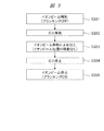
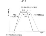
実施の形態1におけるデバイス製造方法について、図3〜図6を用いて説明する。図3は、実施の形態1におけるデバイス製造方法の手順の一例を示すフローチャートである。図4は、スポットビーム方式の場合におけるデバイス製造方法の手順の一例を示すフローチャートである。図5は、プロジェクションビーム方式の場合におけるデバイス製造方法の手順の一例を示すフローチャートである。図6は、図5において、各工程における加工状態の一例を示す説明図である。
<Device manufacturing method>
A device manufacturing method according to the first embodiment will be described with reference to FIGS. FIG. 3 is a flowchart showing an example of the procedure of the device manufacturing method according to the first embodiment. FIG. 4 is a flowchart showing an example of the procedure of the device manufacturing method in the case of the spot beam method. FIG. 5 is a flowchart showing an example of the procedure of the device manufacturing method in the case of the projection beam method. FIG. 6 is an explanatory diagram showing an example of a processing state in each step in FIG.
本実施の形態1におけるデバイス製造方法は、上述(図1)したFIB装置を有するデバイス製造装置を、上述(図2)したデバイス製造装置のソフトウェア構成を構築する加工制御プログラムを実行することで実現可能となるものである。 The device manufacturing method according to the first embodiment is realized by executing a processing control program for building the software configuration of the device manufacturing apparatus described above (FIG. 2) on the device manufacturing apparatus having the FIB apparatus described above (FIG. 1). It is possible.
FIB加工(成膜、エッチング)においては、上述した図16で示したように、設定エリア外への加工が進行する原因は、ブランキング時にアシストガスが試料13に供給されていることである。そこで、本実施の形態においては、図3に示すように、イオンビーム照射(ブランキングOFF)後にガス供給を行い、ガス停止後にイオンビーム停止(ブランキングON)を行うフローに変更することで、上述した改善の余地で説明した課題を解決することが可能となる。
In FIB processing (film formation and etching), as shown in FIG. 16 described above, the cause of processing outside the set area is that the assist gas is supplied to the
すなわち、本実施の形態におけるデバイス製造方法では、図3に示すように、まず、FIB装置は、試料13へイオンビーム7を照射する(工程S101)。この工程S101は、ブランキング制御により行われる。この工程S101では、ブランキング制御装置28の制御により、ブランキング電極8に電圧を印加しないブランキングOFF状態で行われ、試料13へイオンビーム7の照射を開始する。ブランキングOFF状態では、ブランキング電極8による影響がないので、イオンビーム7は試料13に到達する。
That is, in the device manufacturing method according to the present embodiment, as shown in FIG. 3, the FIB apparatus first irradiates the
次に、FIB装置は、試料13へガスを供給する(工程S102)。この工程S102では、ガス源制御装置23の制御により、試料13へガス源17からガスの供給を開始する。この工程S102は、ガスの供給方向を制御することにより行われる。
Next, the FIB apparatus supplies gas to the sample 13 (step S102). In step S <b> 102, supply of gas from the
次に、FIB装置は、ガスが供給された試料13にイオンビーム7を照射することで試料13を加工する(工程S103)。この工程S103では、ガス源制御装置23の制御によりガス源17からガスを供給しながら、ビーム制御部37の制御によりイオンビーム7をスキャンすることで、試料13を加工する。
Next, the FIB apparatus processes the
次に、FIB装置は、試料13へのガスの供給を停止する(工程S104)。この工程S104では、ガス源制御装置23の制御により、試料13へのガス源17からのガスの供給を終了する。この工程S104は、ガスの供給方向を制御することにより行われる。
Next, the FIB apparatus stops the gas supply to the sample 13 (step S104). In step S <b> 104, the supply of the gas from the
次に、FIB装置は、試料13へのイオンビーム7の照射を停止する(工程S105)。この工程S105は、ブランキング制御により行われる。この工程S105では、ブランキング制御装置28の制御により、ブランキング電極8に電圧を印加するブランキングON状態で行われ、試料13へのイオンビーム7の照射を終了する。ブランキングON状態では、ブランキング電極8による影響があるので、イオンビーム7の経路が変化し、イオンビーム7はビーム制限アパーチャ4に遮られ、試料13に到達しない。
Next, the FIB apparatus stops the irradiation of the
このように、本実施の形態におけるデバイス製造方法では、イオンビームを照射する工程S101はガスを供給する工程S102より先に行われ、かつ、ガスの供給を停止する工程S104はイオンビームの照射を停止する工程S105より先に行われる。但し、本実施の形態におけるデバイス製造方法においては、前者および後者の両方が成り立つ場合に限らず、どちらか一方が成り立つ場合にも適用できるものである。すなわち、イオンビームを照射する工程S101はガスを供給する工程S102より先に行われる、もしくは、ガスの供給を停止する工程S104はイオンビームの照射を停止する工程S105より先に行われる。 As described above, in the device manufacturing method according to the present embodiment, the ion beam irradiation step S101 is performed before the gas supply step S102, and the gas supply stop step S104 is performed by ion beam irradiation. This is performed prior to the stopping step S105. However, the device manufacturing method according to the present embodiment is not limited to the case where both the former and the latter are satisfied, and can be applied to the case where either one is satisfied. That is, the ion beam irradiation step S101 is performed prior to the gas supply step S102, or the gas supply stop step S104 is performed prior to the ion beam irradiation step S105.
このような手順では、ガスの供給が無い状態で試料13にイオンビーム7を照射するとエッチングが進行するが、上述した図17に示したようなショート不良の発生は回避できる。また、直前にイオンビーム7を照射して成膜した膜がエッチングされるため、そのエッチング後に所望の膜厚が得られるように調整が必要である。この調整には、デバイス製造装置のデータベース32に内蔵の成膜レートのデータに、予め上記エッチング量を登録しておくのが有効である。
In such a procedure, etching proceeds when the
以下において、本実施の形態におけるデバイス製造方法を詳細に説明する。本実施の形態におけるデバイス製造方法は、スポットビーム方式、プロジェクションビーム方式のいずれを用いる場合にも適用可能である。スポットビーム方式は、試料13上に集束されたイオンビーム7を走査して成膜を行う集束ビーム方式である。プロジェクションビーム方式は、成形マスクを用いてマスク図形の形状のイオンビーム7を試料13上に投射し、成膜を行う投射ビーム方式である。両者の動作フローを、上記工程S101〜S105を参照して説明する。
Hereinafter, the device manufacturing method in the present embodiment will be described in detail. The device manufacturing method according to the present embodiment can be applied to either the spot beam method or the projection beam method. The spot beam method is a focused beam method in which film formation is performed by scanning the
スポットビーム方式の場合におけるデバイス製造方法の手順は、図4に示すように、まず、FIB装置は、試料13の加工始点へイオンビーム7を照射する(工程S201)。この工程S201では、上記工程S101と同様に、試料13へイオンビーム7の照射を開始する。
As shown in FIG. 4, the procedure of the device manufacturing method in the case of the spot beam method is as follows. First, the FIB apparatus irradiates the processing start point of the
次に、FIB装置は、試料13へガスを供給する(工程S202)。この工程S202では、上記工程S102と同様に、試料13へガス源17からガスの供給を開始する。
Next, the FIB apparatus supplies gas to the sample 13 (step S202). In step S202, supply of gas from the
次に、FIB装置は、ガスが供給された試料13にイオンビーム7をスキャン(1周目)しながら照射することで試料13を加工する(工程S203)この工程S203では、上記工程S103と同様に、試料13を加工する。
Next, the FIB apparatus processes the
次に、イオンビーム7のスキャン(1周目)が試料13の加工終点に到達したら(工程S204)、FIB装置は、試料13へのガスの供給を停止する(工程S205)。この工程S205では、上記工程S104と同様に、試料13へのガス源17からのガスの供給を終了する。
Next, when the scanning (first round) of the
次に、FIB装置は、試料13へのイオンビーム7の照射を停止する(工程S206)。この工程S206では、上記工程S105と同様に、試料13へのイオンビーム7の照射を終了する。
Next, the FIB apparatus stops the irradiation of the
以上により、イオンビーム7の1周目のスキャンによる試料13の加工が終了する。続けて、工程S207〜S212を上記程S201〜S206と同様に行い、以後、所定のスキャン回数だけ繰り返すことで、スポットビーム方式の場合の加工が完了する。このように、スポットビーム方式の場合には、加工図形を1スキャンする毎にブランキングを行うのが一般的である。
Thus, the processing of the
プロジェクションビーム方式の場合におけるデバイス製造方法の手順は、図5に示すように、まず、FIB装置は、試料13へイオンビーム7を照射する(工程S301)。この工程S301では、上記工程S101と同様に、試料13へイオンビーム7の照射を開始する。
As shown in FIG. 5, the procedure of the device manufacturing method in the case of the projection beam method is as follows. First, the FIB apparatus irradiates the
次に、FIB装置は、試料13へガスを供給する(工程S302)。この工程S302では、上記工程S102と同様に、試料13へガス源17からガスの供給を開始する。
Next, the FIB apparatus supplies gas to the sample 13 (step S302). In step S302, as in step S102, supply of gas from the
次に、FIB装置は、ガスが供給された試料13にイオンビーム7を照射することで試料13を加工する(工程S303)。この工程S303では、上記工程S103と同様に、試料13を加工する。この工程S303では、スポットビーム方式の場合と異なり、イオンビーム7の位置の移動はない。すなわち、プロジェクションビーム方式では、成形マスクを用いてマスク図形の形状のイオンビーム7を試料13上に投射する。
Next, the FIB apparatus processes the
次に、FIB装置は、試料13へのガスの供給を停止する(工程S304)。この工程S304では、上記工程S104と同様に、試料13へのガス源17からのガスの供給を終了する。
Next, the FIB apparatus stops the gas supply to the sample 13 (step S304). In step S304, as in step S104, the supply of gas from the
次に、FIB装置は、試料13へのイオンビーム7の照射を停止する(工程S305)。この工程S305では、上記工程S105と同様に、試料13へのイオンビーム7の照射を終了する。
Next, the FIB apparatus stops the irradiation of the
以上により、プロジェクションビーム方式の場合の加工が完了する。このように、プロジェクションビーム方式の場合には、一旦イオンビーム7の照射を開始してからは、加工終了までイオンビーム7の照射を保持する。
Thus, the processing in the case of the projection beam method is completed. As described above, in the case of the projection beam method, once the irradiation of the
このプロジェクションビーム方式の場合におけるデバイス製造方法では、例えば、図6に示すような各工程における加工状態となる。図6の例では、上記工程S303〜S305を示している。上記工程S303では、図6(a)に示すように、ガス源17のガス供給ノズル41からガス42が供給された試料13に、成形マスク43を用いてマスク図形の形状のイオンビーム7を投射イオンとして照射することで、試料13に膜44が成膜される。上記工程S304では、図6(b)に示すように、試料13へガス源17のガス供給ノズル41からのガス42の供給が終了される。上記工程S305では、図6(c)に示すように、試料13へイオンビーム7の照射が終了される。これにより、試料13に膜44が形成される。
In the device manufacturing method in the case of the projection beam method, for example, the processing state in each process as shown in FIG. 6 is obtained. In the example of FIG. 6, the steps S303 to S305 are shown. In step S303, as shown in FIG. 6A, the
以上において、イオンビーム照射とガス供給との順序について、イオンビーム照射の開始後にガス供給の開始を行うことで、設定エリア外への加工を抑制することができると述べた。但し実際には、ガス供給開始(ガスバルブ開)から、試料表面に安定的にガス供給がなされるまでは、ある程度の時間がかかる(例えば、数十ms〜数百ms程度)。そのため、ガスバルブを開けてから、例えば数ms以内の間にイオンビーム照射を開始しても、設定エリア外への加工はほとんど発生しないと予想される。 As described above, regarding the order of ion beam irradiation and gas supply, it has been stated that processing outside the set area can be suppressed by starting gas supply after the start of ion beam irradiation. However, in practice, it takes some time (for example, about several tens to several hundreds of milliseconds) from the start of gas supply (gas valve opening) until the gas is stably supplied to the sample surface. Therefore, even if ion beam irradiation is started within, for example, several ms after opening the gas valve, it is expected that the processing outside the setting area hardly occurs.
以上説明した本実施の形態1によれば、FIB加工(成膜、エッチング)中のブランキング動作による設定エリア外への加工の進行を抑制することができる。これにより、FIB加工中に、ブランキング動作の影響で、設定エリア以外の領域に対して加工が進行する課題を解決することができる。すなわち、所望の加工位置以外にイオンビーム7が照射されることを回避することができる。
According to the first embodiment described above, it is possible to suppress the progress of processing outside the set area due to the blanking operation during FIB processing (film formation and etching). As a result, it is possible to solve the problem that the machining progresses to an area other than the setting area due to the blanking operation during the FIB machining. That is, it is possible to avoid irradiation with the
[実施の形態2]
実施の形態2について、図7〜図9を用いて説明する。本実施の形態2において、デバイス製造装置は、前記実施の形態1(図1、図2)と同じなので、ここでの説明は省略する。本実施の形態2では、前記実施の形態1と異なるデバイス製造方法について主に説明する。
[Embodiment 2]
The second embodiment will be described with reference to FIGS. In the second embodiment, the device manufacturing apparatus is the same as that in the first embodiment (FIGS. 1 and 2), and the description thereof is omitted here. In the second embodiment, a device manufacturing method different from that of the first embodiment will be mainly described.
<デバイス製造方法>
実施の形態2におけるデバイス製造方法について、図7〜図9を用いて説明する。図7は、実施の形態2におけるデバイス製造方法において、可動シャッタの開閉によるガス供給制御の一例を示す説明図である。図8は、図7の可動シャッタの開閉によるガス供給制御のタイミングの一例を示す説明図である。図9は、実施の形態2におけるデバイス製造方法の各工程における加工状態の一例を示す説明図である。
<Device manufacturing method>
A device manufacturing method according to the second embodiment will be described with reference to FIGS. FIG. 7 is an explanatory diagram showing an example of gas supply control by opening and closing the movable shutter in the device manufacturing method according to the second embodiment. FIG. 8 is an explanatory diagram showing an example of the timing of gas supply control by opening and closing the movable shutter of FIG. FIG. 9 is an explanatory diagram illustrating an example of a processing state in each step of the device manufacturing method according to the second embodiment.
前記実施の形態1では、ガス供給の開始/終了方法について言及していないが、その点に関してさらに改良を加えたのが本実施の形態2である。一般的なFIB装置でのガス供給制御はバルブの開閉により行われる。バルブを開けてから、ガス供給ノズル41内をガス42が満たし、試料13へのガス供給量が安定化するまでには比較的時間がかかる(例えば、数秒単位の待ち時間を設ける)。また、ガス供給を終了する際にも、ガス供給ノズル41内のガス42が開放されるまでの時間を要する。
Although the first embodiment does not mention the gas supply start / end method, the second embodiment is further improved in this respect. Gas supply control in a general FIB apparatus is performed by opening and closing a valve. After opening the valve, it takes a relatively long time (for example, a waiting time of several seconds is provided) until the
これに対して、本実施の形態2では、図7に示すように、ガス供給ノズル41と試料13との間に可動シャッタ46を設け、可動シャッタ46の開閉によってガス供給のON/OFFを制御する。ガスを供給する工程およびガスの供給を停止する工程は、可動シャッタ46の動作により行われる。可動シャッタ46の開閉の動作は、可動シャッタ制御装置47で行う。可動シャッタ制御装置47は、例えば上述した図1に示した計算処理装置31に接続され、FIB装置を制御する制御装置として機能する。
In contrast, in the second embodiment, as shown in FIG. 7, a
可動シャッタ46の動作によりガス供給のON/OFFを制御すれば、ガス供給ノズル41内は常にガス42で満たされているため、図8に示すように、ガス供給のON/OFFを高速化することができる。図8に示すように、可動シャッタ方式は、ガス供給開始コマンドが実行されると、加工時のガス供給量になるまでの時間がバルブ開閉方式に比べて早くなる。また、加工後にガス供給終了コマンドが実行されると、ガス供給量がゼロになるまでの時間がバルブ開閉方式に比べて早くなる。この時、加工(成膜)に必要な時間は両方式ともに同じである。これにより、ガス供給開始コマンド/ガス供給終了コマンドの実行によるガス供給のON/OFFを高速化することが可能となる。
If the gas supply ON / OFF is controlled by the operation of the
図7において、可動シャッタ46とガス供給ノズル41とは互いに分離して配置し、可動シャッタ46はガス供給ノズル41と非接触であることが望ましい。この理由は、FIB装置では昇温されたガス42を用いるため、可動シャッタ46の接触によりガス供給ノズル41やガス42の温度が変化するのを避けるためである。
In FIG. 7, it is desirable that the
本実施の形態2におけるデバイス製造方法では、例えば、図9に示すような各工程における加工状態となる。図9の例では、図9(a)に示すように、可動シャッタ46を開いた状態で、ガス供給ノズル41からガス42が供給された試料13に、イオンビーム7を投射イオンとして照射することで、試料13に膜44が成膜される。図9(b)に示すように、可動シャッタ46を閉じることで、試料13へガス供給ノズル41からのガス42の供給が終了される。図9(c)に示すように、試料13へイオンビーム7の照射が終了される。これにより、試料13に膜44が形成される。
In the device manufacturing method according to the second embodiment, for example, the processing state is as shown in FIG. In the example of FIG. 9, as shown in FIG. 9A, the
以上説明した本実施の形態2においても、前記実施の形態1と同様に、FIB加工(成膜、エッチング)中のブランキング動作による設定エリア外への加工の進行を抑制することができる。特に、本実施の形態2においては、ガス供給ノズル41と試料13との間に可動シャッタ46を設けることで、可動シャッタ46の開閉によってガス供給のON/OFFを高速化することができる。
In the second embodiment described above, similarly to the first embodiment, it is possible to suppress the progress of processing outside the set area due to the blanking operation during FIB processing (film formation and etching). In particular, in the second embodiment, by providing the
[実施の形態3]
実施の形態3について、図10〜図12を用いて説明する。本実施の形態3において、デバイス製造装置は、前記実施の形態1(図1、図2)と比較して、ブランキング電極の構造が異なる。さらに、本実施の形態3はデバイス製造方法が異なる。本実施の形態3では、前記実施の形態1と異なるデバイス製造方法およびブランキング電極の構造について主に説明する。
[Embodiment 3]
The third embodiment will be described with reference to FIGS. In the third embodiment, the device manufacturing apparatus is different from the first embodiment (FIGS. 1 and 2) in the structure of the blanking electrode. Furthermore, the third embodiment differs in the device manufacturing method. In the third embodiment, a device manufacturing method and a blanking electrode structure different from those in the first embodiment will be mainly described.
<デバイス製造方法>
実施の形態3におけるデバイス製造方法について、図10〜図12を用いて説明する。図10は、実施の形態3におけるデバイス製造方法において、ブランキング方向制御の一例を示す説明図である。図11は、実施の形態3において、ブランキング方向制御による図形外エリアへの加工進行の抑制の一例を示す説明図である。図12は、実施の形態3において、ブランキング電極の構造の一例を示す説明図である。
<Device manufacturing method>
A device manufacturing method according to the third embodiment will be described with reference to FIGS. FIG. 10 is an explanatory diagram showing an example of blanking direction control in the device manufacturing method according to the third embodiment. FIG. 11 is an explanatory diagram showing an example of suppression of processing progress to an area outside the figure by blanking direction control in the third embodiment. FIG. 12 is an explanatory diagram showing an example of the structure of the blanking electrode in the third embodiment.
本実施の形態3は、前記実施の形態1、2のアプローチと異なり、ブランキング時にイオンビーム7が試料13上を動作する方向を制御することによって、ブランキング時の加工がデバイス製造時に悪影響をもたらさないようにするものである。すなわち、本実施の形態3は、イオンビーム7を照射する工程またはイオンビーム7の照射を停止する工程において、イオンビーム7が試料13上を動作する方向が複数の選択肢の中から指定される。このイオンビーム7が試料13上を動作する方向の選択肢は、イオンビーム7の複数のブランキング電極8(8a、8b)にそれぞれ印加される電圧の設定により実現される。
In the third embodiment, unlike the approaches of the first and second embodiments, by controlling the direction in which the
本実施の形態3では、例えば図10に示すように、ブランキング時の成膜が、周囲の電極等と干渉しないエリアに成膜されるように、ブランキングの方向を制御する。上述した図17では、基板51(試料13)の絶縁膜52上に電極(A)53、電極(B)54および電極(C)55を成膜する構成において、電極(B)54と電極(C)55とのショート不良が発生していた。これに対して、本実施の形態3においては、図10に示すように、電極(B)54の形成時に、電極(B)54の上端から電極(C)55とは反対の方向へ斜めに筋状の膜54aが成膜されるようにブランキングの方向を制御することで、電極(B)54と電極(C)55とのショートによるデバイス特性の不良を回避することができる。
In the third embodiment, for example, as shown in FIG. 10, the blanking direction is controlled so that the film formation during blanking is formed in an area that does not interfere with surrounding electrodes and the like. In FIG. 17 described above, in the configuration in which the electrode (A) 53, the electrode (B) 54, and the electrode (C) 55 are formed on the insulating
また、例えば図11に示すように、ブランキング時のイオンビーム動作線が、加工図形61の中に含まれるように設定すれば、加工図形外エリアに加工が進行する恐れはない。図11に示すように、加工図形61の加工始点62にイオンビーム7を照射するブランキング解除時には、イオンビームスキャンエリア63の内側方向を加工始点62でのブランキング方向64とする。また、加工終点65でのブランキング時にも、イオンビームスキャンエリア63の内側方向を加工終点65でのブランキング方向66とする。この方法でも、加工図形外エリアへの加工の進行を抑制することができる。
For example, as shown in FIG. 11, if the ion beam operation line at the time of blanking is set so as to be included in the processed figure 61, there is no possibility that the processing proceeds to the area outside the processed figure. As shown in FIG. 11, when blanking is released to irradiate the
ブランキングの方向を制御するには、FIB装置のブランキング電極8(上述した図1参照)の構造を変更すればよい。一般的なFIB装置では、ブランキング電極8として1対の平行平板型電極を用いているため、イオンビーム7を一定方向にのみ動作させることができる。これに対して、本実施の形態3においては、例えば図12((a)は上面図、(b)は鳥瞰図)に示すように、イオンビーム7の進行方向(Z方向)に2対の平行平板型のブランキング電極8a、8bを配置し、上部のブランキング電極8aでイオンビーム7をX方向に動作させ、下部のブランキング電極8bでイオンビーム7をY方向に動作させる機構とする。これにより、ブランキング時の両ブランキング電極8a、8bの印加電圧を制御することで、任意の方向にイオンビーム7を動作させることができる。
In order to control the blanking direction, the structure of the blanking electrode 8 (see FIG. 1 described above) of the FIB device may be changed. In a general FIB apparatus, since a pair of parallel plate electrodes are used as the blanking
以上説明した本実施の形態3においても、前記実施の形態1と同様に、FIB加工(成膜、エッチング)中のブランキング動作による設定エリア外への加工の進行を抑制することができる。特に、本実施の形態3においては、前記実施の形態1、2のアプローチと異なり、ブランキング時にイオンビーム7が試料13上を動作する方向を制御することで、ブランキング時の加工がデバイス製造時に悪影響をもたらさないようにすることができる。
In the third embodiment described above, similarly to the first embodiment, it is possible to suppress the progress of processing outside the set area due to the blanking operation during FIB processing (film formation and etching). In particular, in the third embodiment, unlike the approaches of the first and second embodiments, by controlling the direction in which the
[付記]
本発明は、特許請求の範囲に記載の特徴に加えて、以下の特徴を有する。
[Appendix]
In addition to the features described in the claims, the present invention has the following features.
(1)試料へイオンビームを照射して微細構造体を製造する微細構造体の製造装置であって、
前記試料へ前記イオンビームを照射する制御と、前記試料に前記イオンビームを照射することで前記試料を加工する制御と、前記試料への前記イオンビームの照射を停止する制御と、を行う制御装置を有し、
前記制御装置において、前記イオンビームを照射する制御または前記イオンビームの照射を停止する制御は、前記イオンビームが前記試料上を動作する方向が複数の選択肢の中から指定される、微細構造体の製造装置。
(1) A microstructure manufacturing apparatus for manufacturing a microstructure by irradiating a sample with an ion beam,
A control device that performs control to irradiate the sample with the ion beam, control to process the sample by irradiating the sample with the ion beam, and control to stop irradiation of the ion beam to the sample Have
In the control device, the control for irradiating the ion beam or the control for stopping the irradiation of the ion beam is performed on the fine structure in which a direction in which the ion beam operates on the sample is specified from a plurality of options. manufacturing device.
(2)前記(1)記載の微細構造体の製造装置において、
前記イオンビームが前記試料上を動作する方向の選択肢は、前記イオンビームの複数のブランキング電極にそれぞれ印加される電圧の設定により実現される、微細構造体の製造装置。
(2) In the fine structure manufacturing apparatus according to (1),
An apparatus for manufacturing a fine structure, in which selection of a direction in which the ion beam operates on the sample is realized by setting voltages applied to a plurality of blanking electrodes of the ion beam.
(3)試料へイオンビームを照射して微細構造体を製造する微細構造体の加工制御プログラムであって、
前記試料へ前記イオンビームを照射する工程と、
前記試料へガスを供給する工程と、
前記試料への前記ガスの供給を停止する工程と、
前記試料への前記イオンビームの照射を停止する工程と、
をコンピュータに実行させ、
前記イオンビームを照射する工程は前記ガスを供給する工程より先に行われる、もしくは、前記ガスの供給を停止する工程は前記イオンビームの照射を停止する工程より先に行われる、微細構造体の加工制御プログラム。
(3) A microstructure control program for manufacturing a microstructure by irradiating a sample with an ion beam,
Irradiating the sample with the ion beam;
Supplying a gas to the sample;
Stopping the supply of the gas to the sample;
Stopping irradiation of the ion beam to the sample;
To the computer,
The step of irradiating the ion beam is performed before the step of supplying the gas, or the step of stopping the supply of the gas is performed before the step of stopping the irradiation of the ion beam. Machining control program.
(4)試料へイオンビームを照射して微細構造体を製造する微細構造体の加工制御プログラムであって、
前記試料へ前記イオンビームを照射する工程と、
前記試料に前記イオンビームを照射することで前記試料を加工する工程と、
前記試料への前記イオンビームの照射を停止する工程と、
をコンピュータに実行させ、
前記イオンビームを照射する工程または前記イオンビームの照射を停止する工程において、前記イオンビームが前記試料上を動作する方向が複数の選択肢の中から指定される、微細構造体の加工制御プログラム。
(4) A microstructure control program for manufacturing a microstructure by irradiating a sample with an ion beam,
Irradiating the sample with the ion beam;
Processing the sample by irradiating the sample with the ion beam;
Stopping irradiation of the ion beam to the sample;
To the computer,
A fine structure processing control program in which, in the step of irradiating the ion beam or stopping the irradiation of the ion beam, a direction in which the ion beam operates on the sample is designated from a plurality of options.
以上、本発明者によってなされた発明を実施の形態に基づき具体的に説明したが、本発明は前記実施の形態に限定されるものではなく、その要旨を逸脱しない範囲で種々変更可能であることはいうまでもない。 As mentioned above, the invention made by the present inventor has been specifically described based on the embodiment. However, the present invention is not limited to the embodiment, and various modifications can be made without departing from the scope of the invention. Needless to say.
例えば、前記実施の形態においては、デバイスの一例として、MEMS構造体(MEMS素子)を説明したが、他の微細構造体などにも適用することができる。また、MEMS構造体の一例として、MEMSセンサを説明したが、他のセンサなどにも適用することができる。 For example, in the above-described embodiment, a MEMS structure (MEMS element) has been described as an example of a device. However, the present invention can also be applied to other fine structures. Further, the MEMS sensor has been described as an example of the MEMS structure, but the present invention can also be applied to other sensors.
なお、本発明は上記した実施の形態に限定されるものではなく、様々な変形例が含まれる。例えば、上記した実施の形態は本発明を分かりやすく説明するために詳細に説明したものであり、必ずしも説明した全ての構成を備えるものに限定されるものではない。 In addition, this invention is not limited to above-described embodiment, Various modifications are included. For example, the above-described embodiment has been described in detail for easy understanding of the present invention, and is not necessarily limited to one having all the configurations described.
また、ある実施の形態の構成の一部を他の実施の形態の構成に置き換えることが可能であり、また、ある実施の形態の構成に他の実施の形態の構成を加えることも可能である。また、各実施の形態の構成の一部について、他の構成の追加、削除、置換をすることが可能である。 Further, a part of the configuration of one embodiment can be replaced with the configuration of another embodiment, and the configuration of another embodiment can be added to the configuration of one embodiment. . In addition, it is possible to add, delete, and replace other configurations for a part of the configuration of each embodiment.
1 真空容器
2 イオン源
7 イオンビーム
8、8a、8b ブランキング電極
9 電子銃
10 電子ビーム
13 試料
14 二次粒子検出器
15 試料ステージ
16 プローブ
17 ガス源
18 FIB鏡筒
21 試料ステージ制御装置
22 マニュピレータ制御装置
23 ガス源制御装置
24 二次粒子検出器制御装置
25 アパーチャ回転制御装置
26 イオン源制御装置
27 レンズ制御装置
28 ブランキング制御装置
31 計算処理装置
32 データベース
32a 構造物ライブラリ
32b CADデータ
32c 加工条件データ
33 モード選択画面
34 モード入力部
35 中央制御部
36 ビーム制御データ
37 ビーム制御部
38 ガス制御データ
41 ガス供給ノズル
42 ガス
43 成形マスク
44 膜
46 可動シャッタ
47 可動シャッタ制御装置
51 基板
52 絶縁膜
53〜55 電極
54a 膜
61 加工図形
62 加工始点
63 イオンビームスキャンエリア
64 ブランキング方向
65 加工終点
66 ブランキング方向
DESCRIPTION OF SYMBOLS 1
Claims (15)
前記試料へ前記イオンビームを照射する工程と、
前記試料へガスを供給する工程と、
前記試料への前記ガスの供給を停止する工程と、
前記試料への前記イオンビームの照射を停止する工程と、
を有し、
前記イオンビームを照射する工程は前記ガスを供給する工程より先に行われる、もしくは、前記ガスの供給を停止する工程は前記イオンビームの照射を停止する工程より先に行われる、微細構造体の製造方法。 A method of manufacturing a fine structure by irradiating a sample with an ion beam to produce a fine structure,
Irradiating the sample with the ion beam;
Supplying a gas to the sample;
Stopping the supply of the gas to the sample;
Stopping irradiation of the ion beam to the sample;
Have
The step of irradiating the ion beam is performed before the step of supplying the gas, or the step of stopping the supply of the gas is performed before the step of stopping the irradiation of the ion beam. Production method.
前記ガスが供給された前記試料に前記イオンビームを照射することで前記試料を加工する工程をさらに有する、微細構造体の製造方法。 In the manufacturing method of the fine structure according to claim 1,
A method for manufacturing a microstructure, further comprising a step of processing the sample by irradiating the ion beam to the sample supplied with the gas.
前記イオンビームを照射する工程および前記イオンビームの照射を停止する工程は、ブランキング制御により行われる、微細構造体の製造方法。 In the manufacturing method of the fine structure according to claim 1,
The method of manufacturing a fine structure, wherein the step of irradiating the ion beam and the step of stopping the irradiation of the ion beam are performed by blanking control.
前記ガスを供給する工程および前記ガスの供給を停止する工程は、前記ガスの供給方向を制御することにより行われる、微細構造体の製造方法。 In the manufacturing method of the fine structure according to claim 1,
The process for supplying the gas and the process for stopping the supply of the gas are performed by controlling a supply direction of the gas.
前記ガスを供給する工程および前記ガスの供給を停止する工程は、ガス供給ノズルと前記試料との間に配置される可動シャッタの動作により行われる、微細構造体の製造方法。 In the manufacturing method of the fine structure according to claim 1,
The process for supplying the gas and the process for stopping the supply of the gas are performed by an operation of a movable shutter disposed between a gas supply nozzle and the sample, and the method for manufacturing a fine structure.
前記イオンビームは、成形マスクを用いて形成された投射ビームである、微細構造体の製造方法。 In the manufacturing method of the fine structure according to claim 1,
The method of manufacturing a fine structure, wherein the ion beam is a projection beam formed using a shaping mask.
前記試料へ前記イオンビームを照射する制御と、前記試料へガスを供給する制御と、前記試料への前記ガスの供給を停止する制御と、前記試料への前記イオンビームの照射を停止する制御と、を行う制御装置を有し、
前記制御装置において、前記イオンビームを照射する制御は前記ガスを供給する制御より先に行われる、もしくは、前記ガスの供給を停止する制御は前記イオンビームの照射を停止する制御より先に行われる、微細構造体の製造装置。 A fine structure manufacturing apparatus for manufacturing a fine structure by irradiating a sample with an ion beam,
A control for irradiating the sample with the ion beam, a control for supplying a gas to the sample, a control for stopping the supply of the gas to the sample, and a control for stopping the irradiation of the ion beam to the sample. And a control device for performing
In the control device, the control for irradiating the ion beam is performed before the control for supplying the gas, or the control for stopping the supply of the gas is performed before the control for stopping the irradiation of the ion beam. , Microstructure manufacturing equipment.
前記制御装置において、前記ガスが供給された前記試料に前記イオンビームを照射することで前記試料を加工する制御がさらに行われる、微細構造体の製造装置。 In the manufacturing apparatus of the fine structure according to claim 7,
In the control device, the fine structure manufacturing apparatus is further controlled to process the sample by irradiating the ion beam to the sample supplied with the gas.
前記イオンビームを照射する制御および前記イオンビームの照射を停止する制御は、ブランキング制御により行われる、微細構造体の製造装置。 In the manufacturing apparatus of the fine structure according to claim 7,
The microstructure manufacturing apparatus, wherein the control for irradiating the ion beam and the control for stopping the ion beam irradiation are performed by blanking control.
前記ガスを供給する制御および前記ガスの供給を停止する制御は、前記ガスの供給方向を制御することにより行われる、微細構造体の製造装置。 In the manufacturing apparatus of the fine structure according to claim 7,
The control for supplying the gas and the control for stopping the supply of the gas are performed by controlling the supply direction of the gas.
前記ガスを供給する制御および前記ガスの供給を停止する制御は、ガス供給ノズルと前記試料との間に配置される可動シャッタの動作により行われる、微細構造体の製造装置。 In the manufacturing apparatus of the fine structure according to claim 7,
The control apparatus for supplying the gas and the control for stopping the supply of the gas are performed by an operation of a movable shutter disposed between the gas supply nozzle and the sample, and the microstructure manufacturing apparatus.
前記可動シャッタと前記ガス供給ノズルとは互いに分離して配置される、微細構造体の製造装置。 In the fine structure manufacturing apparatus according to claim 11,
The apparatus for manufacturing a fine structure, wherein the movable shutter and the gas supply nozzle are arranged separately from each other.
前記イオンビームは、成形マスクを用いて形成された投射ビームである、微細構造体の製造装置。 In the manufacturing apparatus of the fine structure according to claim 7,
The apparatus for manufacturing a fine structure, wherein the ion beam is a projection beam formed using a molding mask.
前記試料へ前記イオンビームを照射する工程と、
前記試料に前記イオンビームを照射することで前記試料を加工する工程と、
前記試料への前記イオンビームの照射を停止する工程と、
を有し、
前記イオンビームを照射する工程または前記イオンビームの照射を停止する工程において、前記イオンビームが前記試料上を動作する方向が複数の選択肢の中から指定される、微細構造体の製造方法。 A method of manufacturing a fine structure by irradiating a sample with an ion beam to produce a fine structure,
Irradiating the sample with the ion beam;
Processing the sample by irradiating the sample with the ion beam;
Stopping irradiation of the ion beam to the sample;
Have
In the step of irradiating the ion beam or the step of stopping the irradiation of the ion beam, a method of manufacturing a fine structure, wherein a direction in which the ion beam operates on the sample is specified from a plurality of options.
前記イオンビームが前記試料上を動作する方向の選択肢は、前記イオンビームの複数のブランキング電極にそれぞれ印加される電圧の設定により実現される、微細構造体の製造方法。 In the manufacturing method of the fine structure according to claim 14,
A method of manufacturing a microstructure, wherein the choice of the direction in which the ion beam operates on the sample is realized by setting a voltage applied to each of a plurality of blanking electrodes of the ion beam.
Priority Applications (2)
| Application Number | Priority Date | Filing Date | Title |
|---|---|---|---|
| JP2017046223A JP2018152183A (en) | 2017-03-10 | 2017-03-10 | Method and device for manufacturing fine structure |
| US15/914,513 US10546721B2 (en) | 2017-03-10 | 2018-03-07 | Microstructure manufacturing method and microstructure manufacturing apparatus |
Applications Claiming Priority (1)
| Application Number | Priority Date | Filing Date | Title |
|---|---|---|---|
| JP2017046223A JP2018152183A (en) | 2017-03-10 | 2017-03-10 | Method and device for manufacturing fine structure |
Publications (1)
| Publication Number | Publication Date |
|---|---|
| JP2018152183A true JP2018152183A (en) | 2018-09-27 |
Family
ID=63445540
Family Applications (1)
| Application Number | Title | Priority Date | Filing Date |
|---|---|---|---|
| JP2017046223A Pending JP2018152183A (en) | 2017-03-10 | 2017-03-10 | Method and device for manufacturing fine structure |
Country Status (2)
| Country | Link |
|---|---|
| US (1) | US10546721B2 (en) |
| JP (1) | JP2018152183A (en) |
Family Cites Families (21)
| Publication number | Priority date | Publication date | Assignee | Title |
|---|---|---|---|---|
| US5429730A (en) * | 1992-11-02 | 1995-07-04 | Kabushiki Kaisha Toshiba | Method of repairing defect of structure |
| JP4209675B2 (en) * | 2000-11-29 | 2009-01-14 | エスアイアイ・ナノテクノロジー株式会社 | Ultra fine three-dimensional structure creation method and processing method |
| US6838380B2 (en) * | 2001-01-26 | 2005-01-04 | Fei Company | Fabrication of high resistivity structures using focused ion beams |
| JP2004309605A (en) * | 2003-04-03 | 2004-11-04 | Sii Nanotechnology Inc | Method of correcting defect in photomask |
| JP4253553B2 (en) * | 2003-09-29 | 2009-04-15 | 株式会社日立ハイテクノロジーズ | Method of forming film using charged particle beam, selective etching method, and charged particle beam apparatus |
| JP4828834B2 (en) * | 2004-02-04 | 2011-11-30 | エスアイアイ・ナノテクノロジー株式会社 | Gas spray nozzle for charged particle beam device and charged particle beam device |
| US20080026548A1 (en) * | 2004-04-09 | 2008-01-31 | Noriaki Tani | Film Forming Apparatus and Film Forming Method |
| JP2006331847A (en) * | 2005-05-26 | 2006-12-07 | Hitachi High-Technologies Corp | Ion beam machining/observation device and method |
| JP5099291B2 (en) * | 2006-02-14 | 2012-12-19 | エスアイアイ・ナノテクノロジー株式会社 | Focused ion beam apparatus and sample cross-section processing and observation method |
| DE102008020145B4 (en) * | 2007-04-23 | 2012-11-08 | Hitachi High-Technologies Corporation | An ion beam processing and viewing device and method for processing and viewing a sample |
| DE102007054073A1 (en) * | 2007-11-13 | 2009-05-14 | Carl Zeiss Nts Gmbh | System and method for editing an object |
| WO2009089499A2 (en) * | 2008-01-09 | 2009-07-16 | Fei Company | Multibeam system |
| JP5074226B2 (en) * | 2008-02-16 | 2012-11-14 | エスアイアイ・ナノテクノロジー株式会社 | Charged particle beam equipment |
| EP2233907A1 (en) * | 2009-03-27 | 2010-09-29 | FEI Company | Forming an image while milling a work piece |
| JP2011210492A (en) | 2010-03-29 | 2011-10-20 | Sii Nanotechnology Inc | Focused ion beam device |
| JP6219019B2 (en) * | 2011-02-25 | 2017-10-25 | エフ・イ−・アイ・カンパニー | Fast switching method between large current mode and small current mode in charged particle beam system |
| JP2013020918A (en) * | 2011-07-14 | 2013-01-31 | Hitachi High-Technologies Corp | Charged particle beam device |
| US9620333B2 (en) * | 2014-08-29 | 2017-04-11 | Hitachi High-Tech Science Corporation | Charged particle beam apparatus |
| US9799490B2 (en) * | 2015-03-31 | 2017-10-24 | Fei Company | Charged particle beam processing using process gas and cooled surface |
| US20170002467A1 (en) * | 2015-07-02 | 2017-01-05 | Fei Company | Adaptive control for charged particle beam processing |
| US10497540B2 (en) * | 2017-01-09 | 2019-12-03 | Tel Epion Inc. | Compensated location specific processing apparatus and method |
-
2017
- 2017-03-10 JP JP2017046223A patent/JP2018152183A/en active Pending
-
2018
- 2018-03-07 US US15/914,513 patent/US10546721B2/en active Active
Also Published As
| Publication number | Publication date |
|---|---|
| US20180261427A1 (en) | 2018-09-13 |
| US10546721B2 (en) | 2020-01-28 |
Similar Documents
| Publication | Publication Date | Title |
|---|---|---|
| EP2530700B1 (en) | Method for preparing thin samples for TEM imaging | |
| JP5173142B2 (en) | Repetitive circumferential cutting for sample preparation | |
| JP5033314B2 (en) | Ion beam processing apparatus and processing method | |
| US20150179402A1 (en) | Method for preparing samples for imaging | |
| KR101550921B1 (en) | Section processing method and its apparatus | |
| TW202145288A (en) | Filling empty structures with deposition under high-energy sem for uniform de layering | |
| CN108573844B (en) | Method for controlling focused ion beam apparatus and recording medium | |
| JP6207081B2 (en) | Focused ion beam device | |
| JP6239401B2 (en) | Charged particle beam equipment | |
| JP2018152183A (en) | Method and device for manufacturing fine structure | |
| CN106683968B (en) | Method for optimizing a charged particle beam formed by shaped holes | |
| EP3101679B1 (en) | Dynamic creation of backup fiducials | |
| JP2007329043A (en) | Drawing plate for charged particle beam and its manufacturing method | |
| JP6300553B2 (en) | Charged particle beam equipment | |
| JP6703903B2 (en) | Microstructure processing method and microstructure processing apparatus | |
| JP6772088B2 (en) | Manufacturing method of microstructure and ion beam device | |
| JP2001007079A (en) | Processing method using ion beam | |
| JP5792767B2 (en) | Ion beam processing apparatus and processing method | |
| JP6814109B2 (en) | Microstructure processing method and microstructure processing equipment | |
| JP6722130B2 (en) | Control method of focused ion beam device | |
| JP4755053B2 (en) | Wiring correction method | |
| WO2017183126A1 (en) | Device machining method and device machining apparatus | |
| JP2017020106A (en) | Adaptive beam current for high-throughput pattern formation | |
| JP2017162811A (en) | Method for structuring object and associated particle beam system | |
| JP2005172565A (en) | Specimen machining method, specimen machining apparatus, and specimen machining program |