JP2018093717A - Excessive voltage prevention device and method - Google Patents
Excessive voltage prevention device and method Download PDFInfo
- Publication number
- JP2018093717A JP2018093717A JP2017230778A JP2017230778A JP2018093717A JP 2018093717 A JP2018093717 A JP 2018093717A JP 2017230778 A JP2017230778 A JP 2017230778A JP 2017230778 A JP2017230778 A JP 2017230778A JP 2018093717 A JP2018093717 A JP 2018093717A
- Authority
- JP
- Japan
- Prior art keywords
- patient
- bias
- voltage
- resistor
- limiting device
- Prior art date
- Legal status (The legal status is an assumption and is not a legal conclusion. Google has not performed a legal analysis and makes no representation as to the accuracy of the status listed.)
- Granted
Links
- 238000000034 method Methods 0.000 title claims description 10
- 230000002265 prevention Effects 0.000 title abstract 3
- 230000001052 transient effect Effects 0.000 claims abstract description 42
- 230000004044 response Effects 0.000 claims abstract description 10
- 230000002457 bidirectional effect Effects 0.000 claims description 34
- 239000003990 capacitor Substances 0.000 claims description 23
- 230000005669 field effect Effects 0.000 claims description 5
- 229910044991 metal oxide Inorganic materials 0.000 claims description 5
- 150000004706 metal oxides Chemical class 0.000 claims description 5
- 239000004065 semiconductor Substances 0.000 claims description 5
- 230000000004 hemodynamic effect Effects 0.000 description 16
- 230000009977 dual effect Effects 0.000 description 8
- 230000001629 suppression Effects 0.000 description 7
- 241001465754 Metazoa Species 0.000 description 6
- 230000015556 catabolic process Effects 0.000 description 5
- 238000013459 approach Methods 0.000 description 4
- 230000008901 benefit Effects 0.000 description 4
- 230000000747 cardiac effect Effects 0.000 description 4
- 230000000638 stimulation Effects 0.000 description 4
- 206010061592 cardiac fibrillation Diseases 0.000 description 2
- 238000012544 monitoring process Methods 0.000 description 2
- 210000005036 nerve Anatomy 0.000 description 2
- 230000001681 protective effect Effects 0.000 description 2
- 230000009467 reduction Effects 0.000 description 2
- 230000000903 blocking effect Effects 0.000 description 1
- 238000010586 diagram Methods 0.000 description 1
- 230000002600 fibrillogenic effect Effects 0.000 description 1
- 210000005003 heart tissue Anatomy 0.000 description 1
- 238000010348 incorporation Methods 0.000 description 1
- 230000002452 interceptive effect Effects 0.000 description 1
- 238000005259 measurement Methods 0.000 description 1
- 238000012986 modification Methods 0.000 description 1
- 230000004048 modification Effects 0.000 description 1
- 230000001537 neural effect Effects 0.000 description 1
- 230000035945 sensitivity Effects 0.000 description 1
Images


Classifications
-
- H—ELECTRICITY
- H02—GENERATION; CONVERSION OR DISTRIBUTION OF ELECTRIC POWER
- H02H—EMERGENCY PROTECTIVE CIRCUIT ARRANGEMENTS
- H02H9/00—Emergency protective circuit arrangements for limiting excess current or voltage without disconnection
- H02H9/04—Emergency protective circuit arrangements for limiting excess current or voltage without disconnection responsive to excess voltage
- H02H9/045—Emergency protective circuit arrangements for limiting excess current or voltage without disconnection responsive to excess voltage adapted to a particular application and not provided for elsewhere
-
- A—HUMAN NECESSITIES
- A61—MEDICAL OR VETERINARY SCIENCE; HYGIENE
- A61B—DIAGNOSIS; SURGERY; IDENTIFICATION
- A61B5/00—Measuring for diagnostic purposes; Identification of persons
- A61B5/24—Detecting, measuring or recording bioelectric or biomagnetic signals of the body or parts thereof
- A61B5/30—Input circuits therefor
- A61B5/301—Input circuits therefor providing electrical separation, e.g. by using isolating transformers or optocouplers
-
- A—HUMAN NECESSITIES
- A61—MEDICAL OR VETERINARY SCIENCE; HYGIENE
- A61N—ELECTROTHERAPY; MAGNETOTHERAPY; RADIATION THERAPY; ULTRASOUND THERAPY
- A61N1/00—Electrotherapy; Circuits therefor
- A61N1/02—Details
- A61N1/08—Arrangements or circuits for monitoring, protecting, controlling or indicating
-
- A—HUMAN NECESSITIES
- A61—MEDICAL OR VETERINARY SCIENCE; HYGIENE
- A61N—ELECTROTHERAPY; MAGNETOTHERAPY; RADIATION THERAPY; ULTRASOUND THERAPY
- A61N1/00—Electrotherapy; Circuits therefor
- A61N1/18—Applying electric currents by contact electrodes
- A61N1/32—Applying electric currents by contact electrodes alternating or intermittent currents
- A61N1/36—Applying electric currents by contact electrodes alternating or intermittent currents for stimulation
- A61N1/3605—Implantable neurostimulators for stimulating central or peripheral nerve system
- A61N1/36125—Details of circuitry or electric components
-
- A—HUMAN NECESSITIES
- A61—MEDICAL OR VETERINARY SCIENCE; HYGIENE
- A61N—ELECTROTHERAPY; MAGNETOTHERAPY; RADIATION THERAPY; ULTRASOUND THERAPY
- A61N1/00—Electrotherapy; Circuits therefor
- A61N1/18—Applying electric currents by contact electrodes
- A61N1/32—Applying electric currents by contact electrodes alternating or intermittent currents
- A61N1/36—Applying electric currents by contact electrodes alternating or intermittent currents for stimulation
- A61N1/3605—Implantable neurostimulators for stimulating central or peripheral nerve system
- A61N1/36128—Control systems
- A61N1/36142—Control systems for improving safety
-
- A—HUMAN NECESSITIES
- A61—MEDICAL OR VETERINARY SCIENCE; HYGIENE
- A61N—ELECTROTHERAPY; MAGNETOTHERAPY; RADIATION THERAPY; ULTRASOUND THERAPY
- A61N1/00—Electrotherapy; Circuits therefor
- A61N1/18—Applying electric currents by contact electrodes
- A61N1/32—Applying electric currents by contact electrodes alternating or intermittent currents
- A61N1/36—Applying electric currents by contact electrodes alternating or intermittent currents for stimulation
- A61N1/362—Heart stimulators
- A61N1/37—Monitoring; Protecting
- A61N1/3718—Monitoring of or protection against external electromagnetic fields or currents
-
- A—HUMAN NECESSITIES
- A61—MEDICAL OR VETERINARY SCIENCE; HYGIENE
- A61N—ELECTROTHERAPY; MAGNETOTHERAPY; RADIATION THERAPY; ULTRASOUND THERAPY
- A61N1/00—Electrotherapy; Circuits therefor
- A61N1/18—Applying electric currents by contact electrodes
- A61N1/32—Applying electric currents by contact electrodes alternating or intermittent currents
- A61N1/38—Applying electric currents by contact electrodes alternating or intermittent currents for producing shock effects
- A61N1/39—Heart defibrillators
- A61N1/3925—Monitoring; Protecting
-
- H—ELECTRICITY
- H02—GENERATION; CONVERSION OR DISTRIBUTION OF ELECTRIC POWER
- H02H—EMERGENCY PROTECTIVE CIRCUIT ARRANGEMENTS
- H02H9/00—Emergency protective circuit arrangements for limiting excess current or voltage without disconnection
- H02H9/005—Emergency protective circuit arrangements for limiting excess current or voltage without disconnection avoiding undesired transient conditions
-
- H—ELECTRICITY
- H03—ELECTRONIC CIRCUITRY
- H03K—PULSE TECHNIQUE
- H03K17/00—Electronic switching or gating, i.e. not by contact-making and –breaking
- H03K17/08—Modifications for protecting switching circuit against overcurrent or overvoltage
- H03K17/081—Modifications for protecting switching circuit against overcurrent or overvoltage without feedback from the output circuit to the control circuit
- H03K17/08104—Modifications for protecting switching circuit against overcurrent or overvoltage without feedback from the output circuit to the control circuit in field-effect transistor switches
-
- A—HUMAN NECESSITIES
- A61—MEDICAL OR VETERINARY SCIENCE; HYGIENE
- A61B—DIAGNOSIS; SURGERY; IDENTIFICATION
- A61B2562/00—Details of sensors; Constructional details of sensor housings or probes; Accessories for sensors
- A61B2562/18—Shielding or protection of sensors from environmental influences, e.g. protection from mechanical damage
Landscapes
- Health & Medical Sciences (AREA)
- Life Sciences & Earth Sciences (AREA)
- Engineering & Computer Science (AREA)
- Public Health (AREA)
- Veterinary Medicine (AREA)
- Biomedical Technology (AREA)
- Animal Behavior & Ethology (AREA)
- General Health & Medical Sciences (AREA)
- Nuclear Medicine, Radiotherapy & Molecular Imaging (AREA)
- Radiology & Medical Imaging (AREA)
- Heart & Thoracic Surgery (AREA)
- Neurology (AREA)
- Cardiology (AREA)
- Physics & Mathematics (AREA)
- Neurosurgery (AREA)
- Molecular Biology (AREA)
- Biophysics (AREA)
- Pathology (AREA)
- Medical Informatics (AREA)
- Surgery (AREA)
- Power Engineering (AREA)
- Electromagnetism (AREA)
- Electrotherapy Devices (AREA)
- Emergency Protection Circuit Devices (AREA)
Abstract
Description
本明細書は、一般には、過電圧保護装置又は回路及び方法に関し、特に、過電圧保護装置、及び電気又は電子医療機器のための方法に関する。 This specification relates generally to overvoltage protection devices or circuits and methods, and more particularly to overvoltage protection devices and methods for electrical or electronic medical devices.
医療及び獣医用途向けの能動的な電気装置は、通常、特定の目的のために使用される。ECGモニタは心電図を取得するために使用され、電気的インピーダンスの測定による血行動態モニタは電気補助電流を印加し、電気焼灼ナイフ及び他の電気外科装置が手術室で使用され、電気パルス発生器は心臓組織又は神経を刺激するために電気刺激を与え、心臓細動除去器は細動を克服するために心臓に向かって高電圧パルスを印加する。そのような装置が、同じ患者に同時に複数使用されることは多い。そのため、他の機器によって適用された電気エネルギーが原因となり、各電気又は電子医療機器が損傷しないように保護することが重要である(「保護の必要性(protection requirement)」)。電子医療機器は、患者や動物の治療のために他の機器によって加えられたエネルギーを吸収しないように設計されなければならない(「エネルギー低減の必要性(energy reduction requirement)」)。 Active electrical devices for medical and veterinary applications are usually used for specific purposes. An ECG monitor is used to acquire an electrocardiogram, a hemodynamic monitor by measuring electrical impedance applies an electrical assist current, an electrocautery knife and other electrosurgical devices are used in the operating room, and an electrical pulse generator Electrical stimulation is applied to stimulate heart tissue or nerves, and a cardiac defibrillator applies high voltage pulses toward the heart to overcome fibrillation. Often, multiple such devices are used simultaneously on the same patient. Therefore, it is important to protect each electrical or electronic medical device from being damaged due to electrical energy applied by other devices ("protection requirement"). Electronic medical devices must be designed so that they do not absorb energy added by other devices for the treatment of patients or animals ("energy reduction requirement").
患者又は動物に同時に適用される電気装置間の互換性は、除細動パルスを患者に印加する際に特に重要である。数百ボルトから数千ボルト(「過電圧」)に達する電圧振幅を有する除細動パルスによって、同時に使用される他の電子医療機器に対する課題が生じる。この課題は、電気パルス(ペースメーカ)又は信号波形(患者補助電流)を放出する装置にとって大きな課題である。このような装置は、患者(又は動物)に対して低インピーダンスのインターフェースを有する。例えば、ペースメーカが、通常、患者側配線インターフェース(patient line interfaces)の低インピーダンスを示す2つの状態は、刺激パルス及び刺激パルスの直後の放電期間中である。ペースメーカは数オームの範囲内の患者側配線インターフェースインピーダンスを必要とするが、バイオインピーダンスベースのモニタは、典型的には、数百オームから最大約1キロオームのインピーダンスで作動する。すなわち、保護上の理由からインターフェースに加えられるインピーダンスは、発信装置の機能を損なう可能性がある。 Compatibility between electrical devices applied simultaneously to a patient or animal is particularly important when applying a defibrillation pulse to the patient. Defibrillation pulses with voltage amplitudes that reach hundreds to thousands of volts ("overvoltage") create challenges for other electronic medical devices that are used simultaneously. This challenge is a major challenge for devices that emit electrical pulses (pacemaker) or signal waveforms (patient auxiliary current). Such devices have a low impedance interface to the patient (or animal). For example, two conditions where pacemakers typically exhibit low impedance in patient line interfaces are during the stimulation pulse and the discharge period immediately following the stimulation pulse. While pacemakers require patient-side wiring interface impedances in the range of a few ohms, bioimpedance-based monitors typically operate with impedances from a few hundred ohms up to about 1 kilohm. That is, the impedance applied to the interface for protection reasons can impair the function of the transmitter.
除細動パルスに対する簡単な保護は、患者(人間又は動物)側配線インターフェースと直列の「保護抵抗」と共に過渡電圧抑制ダイオード(TVS)を使用することによって可能となり、各患者側配線インターフェースに適用することができる。適切に除細動エネルギーを減少させるためには、除細動保護抵抗の値を小さくすることはできない。その代わりに、相対的に高抵抗の抵抗が必要となる。このように、この単純な除細動保護アプローチは、低インピーダンスインターフェースを必要とする心臓ペースメーカ及びバイオインピーダンスベースのモニタなどの能動的な電気装置には使用することができない。 Simple protection against defibrillation pulses is made possible by using a transient voltage suppression diode (TVS) with a “protection resistor” in series with the patient (human or animal) side wiring interface and applies to each patient side wiring interface. be able to. In order to properly reduce the defibrillation energy, the value of the defibrillation protection resistance cannot be reduced. Instead, a relatively high resistance is required. Thus, this simple defibrillation protection approach cannot be used for active electrical devices such as cardiac pacemakers and bioimpedance based monitors that require a low impedance interface.
通常の動作中に低インピーダンスの患者インターフェースと過電圧生成時に高インピーダンスインターフェースとを切り替えるために一般的に使用されるアプローチは、患者インターフェースに沿ってデプリーション型金属酸化物半導体電界効果トランジスタ(MOSFET)を使用することである。MOSFETがオフ状態のときに流れる電流が最小になるので、これらの装置は電流を制限するものとして機能する。 A commonly used approach to switching between a low impedance patient interface during normal operation and a high impedance interface during overvoltage generation uses a depletion-type metal oxide semiconductor field effect transistor (MOSFET) along the patient interface It is to be. These devices function as current limiting because the current that flows when the MOSFET is off is minimized.
医療機器用の多くの公知の過電圧保護回路は、患者側配線インターフェースと直列の素子を有しており、MOSFETトランジスタをバイアスして電流を十分に妨げることができる。この素子は、抵抗又は他のトランジスタを含むことができる。どちらの場合でも、この素子は、通常の動作中の患者側配線インターフェースのインピーダンスを、トランジスタを使用するより少ない量だけ増加させ、抵抗を使用するより多くの量を増加させる。この欠点に加えて、いくつかの解決策は、保護された装置自体によって生成されるバイアス電圧に依存する、比較的複雑なMOSFETバイアス技術を採用する。保護が内部電圧に依存しており、内部電圧は障害又はバッテリの消耗によって疑わしいレベルになることがあるので、これにより損傷が発生することがある。 Many known overvoltage protection circuits for medical devices have an element in series with the patient-side wiring interface and can bias the MOSFET transistor to sufficiently block current. The element can include a resistor or other transistor. In either case, this element increases the impedance of the patient-side wiring interface during normal operation by a smaller amount than using transistors and increases the larger amount using resistors. In addition to this drawback, some solutions employ relatively complex MOSFET bias techniques that rely on the bias voltage generated by the protected device itself. This can cause damage because protection depends on the internal voltage, which can be at a suspicious level due to faults or battery drain.
いくつかの保護回路は、各患者側配線インターフェースと直列のコンデンサを有する。コンデンサは、最初の過電圧過渡エネルギーの一部しか通過しないように、入力トランジェントの形状を変化させる。残りの電圧は、ツェナーダイオードなどの電圧制限装置によってクランプされる。コンデンサとツェナーダイオードを組み合わせると、入力エネルギーが反発する。このような回路の潜在的な欠点は、コンデンサに関連する。高電圧トランジェントに対する信頼性の高い保護は、通常のタイプではない特殊な高電圧コンデンサの使用を必要とするため、多くの場合は高価であるか、及び/又は、手に入れるのが困難である。他の潜在的な欠点は、保護回路の感度が、印加される容量値に依存することである。このような保護回路は、予想される過電圧過渡状態を考慮してトリミングすることができるが、過電圧保護回路の所望の特性ではない。さらに、各患者側配線インターフェースに直列に接続された必要なコンデンサはインピーダンスを構成し、その値は容量値にも依存する。 Some protection circuits have a capacitor in series with each patient-side wiring interface. The capacitor changes the shape of the input transient so that only a portion of the initial overvoltage transient energy passes. The remaining voltage is clamped by a voltage limiting device such as a Zener diode. When a capacitor and a Zener diode are combined, the input energy is repelled. A potential drawback of such circuits is associated with capacitors. Reliable protection against high voltage transients is often expensive and / or difficult to obtain because it requires the use of special high voltage capacitors that are not of the usual type . Another potential drawback is that the sensitivity of the protection circuit depends on the applied capacitance value. Such a protection circuit can be trimmed in view of an expected overvoltage transient, but is not a desired characteristic of an overvoltage protection circuit. Furthermore, the necessary capacitors connected in series to each patient-side wiring interface constitute an impedance, the value of which also depends on the capacitance value.
一実施態様では、患者インターフェースと電子医療機器との間の過電圧保護回路は、患者電流経路又は配線に配置されたデプリーション型金属酸化物半導体電界効果トランジスタ(MOSFET)のような電流制限装置を組み合わせて使用され、過渡電圧パルスの場合に関連するMOSFETをオフにするためにバイアス電圧を生成するように構成された回路を有する。一実施態様では、バイアス電圧は、一端で患者電流経路又は患者側配線インターフェースに接続され、過渡電圧抑制装置(TVS:transient voltage suppressor)と直列に患者側配線から延在するバイアス抵抗から得られる。TVSは、一方向性又は双方向性のTVS又は分圧器を形成するためのバイアス抵抗と直列の第2の抵抗であってもよい。この構成では、保護構成要素は、医療機器の作動可能な電子構成要素と患者インターフェースとの間に接続された患者側配線に直接配置されない。 In one embodiment, an overvoltage protection circuit between a patient interface and an electronic medical device combines a current limiting device such as a depletion metal oxide semiconductor field effect transistor (MOSFET) disposed in a patient current path or wiring. Used to have a circuit configured to generate a bias voltage to turn off the associated MOSFET in case of transient voltage pulses. In one embodiment, the bias voltage is derived from a bias resistor connected at one end to the patient current path or patient side wiring interface and extending from the patient side wiring in series with a transient voltage suppressor (TVS). The TVS may be a second resistor in series with a bias resistor to form a unidirectional or bidirectional TVS or voltage divider. In this configuration, the protective component is not placed directly on the patient side wiring connected between the operable electronic component of the medical device and the patient interface.
他の実施態様では、1つ以上の電子部品と、電気信号を医療機器の電子部品に及び/又は電子機器を接続するための第1及び第2の患者側配線を有する少なくとも1つの患者チャネルと、患者チャネルに接続された患者インターフェースと、患者チャネルに関連付けられ、第1の患者側配線又は電流経路に配置された第1の電流制限装置、第2の患者側配線に配置された第2の電流制限装置、並びに第1及び第2の患者側配線のそれぞれの外側にある第1及び第2のバイアス電圧生成装置を有し、第1又は第2の配線の過渡過電圧に応答して、第1又は第2の電流制限装置をオフにして、それぞれ第1又は第2の配線を流れる電流を制限するために、所定のバイアス電圧を生成するように構成される過電圧保護装置又は回路と、を有する医療機器が提供される。 In other embodiments, one or more electronic components and at least one patient channel having first and second patient-side wiring for connecting electrical signals to and / or connecting electronic devices to medical devices A patient interface connected to the patient channel; a first current limiter associated with the patient channel and disposed in the first patient-side wiring or current path; a second disposed in the second patient-side wiring In response to a transient overvoltage in the first or second wiring, the current limiting device and the first and second bias voltage generating devices outside the first and second patient-side wirings, respectively. An overvoltage protection device or circuit configured to generate a predetermined bias voltage to turn off the one or second current limiting device and limit the current flowing through the first or second wiring, respectively; Medical care Vessel is provided.
一実施態様では、第1及び第2の電圧生成装置は、一端がそれぞれの第1又は第2の患者側配線に接続されたそれぞれの第1及び第2のバイアス抵抗と、それぞれの第1及び第2のバイアス抵抗の間に直列に接続された少なくとも1つの電圧制限装置又は過渡電圧抑制装置を有する。一実施形態では、電圧制限装置は、バイアス抵抗の第2の端部の間に接続された1つの双方向性の電圧制限装置を有する。他の実施形態では、第1の一方向性の電圧制限装置が第1のバイアス抵抗に接続され、第2の一方向性の電圧制限装置が第2のバイアス抵抗に接続され、第1及び第2の一方向性の電圧制限装置が互いに接続される。他の実施形態では、第1及び第2のバイアス抵抗はそれぞれ第1及び第2の分圧器を形成するためにそれぞれ追加の抵抗と直列に接続され、それぞれ第1の電流制限装置に接続された第1の分圧器の抵抗間の接続部を有し、それぞれ第2の電流制限装置に接続された第2の分圧器の抵抗間の接続部を有する。 In one embodiment, the first and second voltage generators include respective first and second bias resistors, one end of which is connected to the respective first or second patient-side wiring, and the first and second bias resistors. At least one voltage limiting device or transient voltage suppression device connected in series between the second bias resistors. In one embodiment, the voltage limiting device has one bidirectional voltage limiting device connected between the second ends of the bias resistors. In another embodiment, a first unidirectional voltage limiting device is connected to the first bias resistor, a second unidirectional voltage limiting device is connected to the second bias resistor, and the first and second Two unidirectional voltage limiting devices are connected to each other. In other embodiments, the first and second bias resistors are each connected in series with additional resistors to form first and second voltage dividers, respectively, and are each connected to the first current limiter. It has a connection between the resistors of the first voltage divider, each having a connection between the resistors of the second voltage divider connected to the second current limiting device.
一実施形態では、バイアス抵抗は、過渡電圧抑制ダイオード(TVS)と直列に接続され、MOSFETソースとゲート端子との間にも接続されている。急峻なランプの形状を有する過電圧が発生すると、最初は小さな電流が抵抗を通って流れる。この抵抗の両端の電圧がMOSFETの必要バイアスレベルに達すると、MOSFETは患者側配線インターフェースを遮断し、その結果、電流が抵抗を通って流れる。TVSの電圧制限機能は、過渡過電圧の最初に、TVSと直列に接続された抵抗を流れる電流を小さくするために必要である。他の実施形態では、TVSを抵抗で置き換えることができる。他の実施形態では、バイアス抵抗は第2の抵抗と直列に接続されて分圧器を形成し、MOSFETゲート端子に接続された抵抗の間の接続部を形成する。 In one embodiment, the bias resistor is connected in series with a transient voltage suppression diode (TVS) and is also connected between the MOSFET source and the gate terminal. When an overvoltage with a steep lamp shape occurs, a small current initially flows through the resistor. When the voltage across this resistor reaches the required bias level of the MOSFET, the MOSFET shuts off the patient-side wiring interface, so that current flows through the resistor. The voltage limiting function of the TVS is necessary to reduce the current flowing through the resistor connected in series with the TVS at the beginning of the transient overvoltage. In other embodiments, the TVS can be replaced by a resistor. In other embodiments, the bias resistor is connected in series with the second resistor to form a voltage divider and form a connection between the resistors connected to the MOSFET gate terminals.
過電圧保護回路又は装置は、過渡過電圧に対して非常に迅速に応答するように設計されている。MOSFETは、過電圧がピークに達する前に、過電圧ランプの開始時にほとんどオフ状態にある。また、バイアス回路は、患者側配線インターフェースに追加のインピーダンス素子を必要としない。 Overvoltage protection circuits or devices are designed to respond very quickly to transient overvoltages. The MOSFET is almost off at the beginning of the overvoltage ramp before the overvoltage reaches its peak. Also, the bias circuit does not require an additional impedance element at the patient side wiring interface.
一実施態様では、過電圧保護回路は、患者側配線インターフェースに1つの構成要素のみを追加し、具体的には、オン状態又はオフ状態のいずれかのMOSFETなどの電流制限装置を追加する。 In one embodiment, the overvoltage protection circuit adds only one component to the patient-side wiring interface, and specifically adds a current limiting device such as a MOSFET that is either on or off.
過電圧保護回路は、電圧/電流信号又はパルス(心臓及び神経刺激器又は生体インピーダンスに基づくモニタなど)を出力(発信)する任意の医療装置に組み込まれ、又はそれと共に使用することができる。これらの装置は、患者(又は動物)に対する低抵抗インターフェースを特徴とする。除細動パルスのような過電圧印加の場合、これらの装置は損傷を非常に受けやすく、患者のために意図された印加エネルギーを患者から遠ざける方向に変える。過電圧保護回路は、配線の除細動パルスなどの過電圧の発生時に関連する患者側配線又は配線を遮断するように設計されている。 The overvoltage protection circuit can be incorporated into or used with any medical device that outputs (transmits) voltage / current signals or pulses (such as monitors based on heart and nerve stimulators or bioimpedance). These devices feature a low resistance interface to the patient (or animal). In the case of an overvoltage application, such as a defibrillation pulse, these devices are very susceptible to damage and turn the applied energy intended for the patient away from the patient. The overvoltage protection circuit is designed to block the associated patient side wiring or wiring when an overvoltage such as a wiring defibrillation pulse occurs.
様々な実施形態の詳細は、部分的に、添付の図面の調べることにより収集することができ、同様の参照番号は同様の部分を指す。 Details of various embodiments can be gathered, in part, by examining the accompanying drawings, wherein like reference numerals refer to like parts.
本明細書で開示される特定の実施形態は、ECGモニタ、血行力学的モニタ、電気焼灼ナイフ又は他の電気外科装置、心臓刺激又は神経刺激のための電気パルス発生器又はペースメーカ、及び心臓細動除去器などを含む埋め込み型又は外部装置など、治療又はモニタリングのための電気医療装置の出力又は入力に接続された1つ以上の患者側配線インターフェースと直接的に接続されない回路部品を介してバイアス電圧を生成するように設計された過電圧保護システム又は回路を提供する。 Certain embodiments disclosed herein include ECG monitors, hemodynamic monitors, electrocautery knives or other electrosurgical devices, electrical pulse generators or pacemakers for cardiac or neural stimulation, and cardiac fibrillation Bias voltage through circuit components not directly connected to one or more patient-side wiring interfaces connected to the output or input of an electro-medical device for treatment or monitoring, such as an implantable or external device including a remover An overvoltage protection system or circuit designed to generate
本明細書に記載された主題は、例示的な実装形態によって示されている。明確のため、主題を不明確にするのを避けるために、様々な詳細は省略されている。以下に示す例は、過電圧保護装置、電子医療機器のためのシステム及び方法を主題としている。主題の特徴及び利点は、以下の説明によって明らかにされる。 The subject matter described in this specification is illustrated by exemplary implementations. For clarity, various details have been omitted to avoid obscuring the subject matter. The following examples are directed to overvoltage protection devices, systems and methods for electronic medical devices. The features and advantages of the subject matter will become apparent from the description that follows.
本明細書によって、当業者に対しては、様々な他の実施形態及び他の応用として本発明をどのように実施するかが明らかになる。しかしながら、本明細書は、本発明に関する様々な全ての実施形態を説明するものではない。本明細書に示された実施形態は、一例として示されているに過ぎず、実施形態を限定するものではない。 The specification will make it apparent to those skilled in the art how to implement the invention in various other embodiments and other applications. However, this description is not intended to describe all of the various embodiments relating to the present invention. The embodiments shown herein are shown by way of example only and do not limit the embodiments.
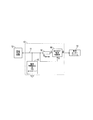
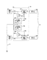
図1は、電子医療機器12と患者インターフェース14との間で患者側配線11に直列に接続された従来技術の回路又は過電圧保護装置10を示している。装置10は、患者側配線11と接地との間に接続された過渡電圧抑制ダイオード(TVS)15、患者側配線インターフェース14と直列に患者側配線11に接続された保護抵抗(インピーダンス)16、MOSFET電流制限器18によって過電圧に対する保護を提供する。この構成では、過電圧パルスが発生すると、MOSFETはオフになる。適切な除細動エネルギーの低減を達成するため、除細動又は過電圧保護抵抗16のオーム値を小さくすることはできない。代わりに、比較的高抵抗の抵抗が必要である。したがって、この単純な除細動保護アプローチは、低インピーダンスインターフェースを必要とする心臓ペースメーカ及び生体適合性ベースのモニタなどの能動的な電気装置には使用することができない。
FIG. 1 shows a prior art circuit or
図2は、患者側配線インターフェース14及び医療機器内部回路12と直列に患者側配線11に抵抗又はインピーダンスを直接有さない過電圧保護装置又は回路20の第1の実施形態を示す。図2の実施形態は、1つの患者側配線インターフェース11を用いて図示されているが、2つの患者インターフェース(1つの患者チャネル)に対する過電圧保護を提供するために、変更された実施形態が提供され、又は、医療装置に設けられたチャネルの数に応じて、2つ、3つ又はそれ以上の患者チャネルの過電圧保護のために提供される。以下に説明する過電圧保護回路は、電子部品と患者インターフェースとの間の電子医療機器自体に組み込まれてもよく、又は医療機器と患者との間に組み込むための別個の装置であってもよい。
FIG. 2 shows a first embodiment of an overvoltage protection device or
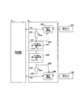
一実施形態では、過電圧保護回路は、患者側配線又は患者電流経路に位置していないバイアス電圧生成装置と組み合わせて、患者側配線又は電流経路内のデプリーション型MOSFETなどの電流制限装置を使用し、過電圧が発生した場合に電流制限装置のバイアス電圧を設定するするように構成される。図2は、動作原理を示すために、1つの患者側配線に関連する過電圧保護回路の一実施形態を示す。この構成では、患者側配線は一方向にのみ保護される。いくつかの変形例については、図3から図12に関連して以下でより詳細に説明するように、各患者チャネルが過電圧保護回路20を有し、過渡電圧の印加方向に依存せずに保護が可能となる。
In one embodiment, the overvoltage protection circuit uses a current limiting device, such as a depletion type MOSFET in the patient wiring or current path, in combination with a bias voltage generator that is not located in the patient wiring or patient current path, A bias voltage of the current limiting device is set when an overvoltage occurs. FIG. 2 shows one embodiment of an overvoltage protection circuit associated with one patient side wiring to illustrate the principle of operation. In this configuration, the patient side wiring is protected in only one direction. For some variations, as will be described in more detail below in connection with FIGS. 3-12, each patient channel has an
図2では、MOSFETなどの電流制限器25が、電気又は電子医療機器の患者インターフェース14と内部回路12との間の電流経路又は第1の配線11に配置されている。バイアス電圧生成回路又は装置は、患者11から延在する第2の配線23に配置され、MOSFET25と医療装置の内部回路との間の位置で患者側配線又は配線11に一端で接続され、配線23のTVSダイオード24のような過渡電圧制限装置と直列に接続されたバイアス抵抗22を有する。バイアス抵抗22とTVSダイオード24との間の接続部は、配線26を介してMOSFETゲート端子Gに接続されている。
In FIG. 2, a
このアプローチでは、MOSFETのバイアス電圧は、MOSFETの電流経路の外に(したがって、患者の電流経路又は患者側配線インターフェースの外側に)配置された抵抗や、特に、過渡電圧抑制器(TVS)と直列に配置された抵抗から得られ、過渡電圧抑制器(TVS)は、一方向性の又は双方向性のTVSのいずれかになる。これは、図1の従来技術の構成とは異なり、MOSFETと装置内部回路12との間の配線11に直列に抵抗素子を接続することを回避する。
In this approach, the bias voltage of the MOSFET is in series with a resistor placed outside the MOSFET's current path (and thus outside the patient's current path or patient-side wiring interface), and in particular with a transient voltage suppressor (TVS). The transient voltage suppressor (TVS) can be either a unidirectional or bidirectional TVS. This avoids connecting a resistance element in series to the
いくつかの実施形態では、バイアス抵抗は、過渡過電圧の場合にMOSFETを比較的迅速にオフにするのに十分なバイアス電圧を生成するように選択された抵抗を有する。いくつかの実施形態では、100オームの抵抗を有する抵抗は、過渡電圧抑制ダイオード(TVS)24と直列に接続されるが、いくつかの実施形態では、例えば50オームから1キロオームの範囲の抵抗を有する異なる抵抗値を有するバイアス抵抗を使用することができる。MOSFET電流経路の外側にTVSダイオード24とともに配置された抵抗22は、デプリーション型MOSFET25のためのバイアス電圧を生成するために使用される。このバイアス電圧は、MOSFET電流制限器のソース端子Sとゲート端子Gとの間の配線11及び配線26を介して印加され、過渡過電圧が患者インターフェースの入力に発生した場合、MOSFET電流制限器をオフにする。デプリーション型MOSFETは、TVSが導通し始めるときに小さな電流が抵抗22を流れ始めるので、過渡電圧パルスの初めに高インピーダンスを示す。典型的な過渡過電圧の電圧の一部分で導通するTVSダイオードが選択される。ペースメーカや血行動態モニタなどの多くの装置では、印加されたTVSは20Vから24Vの電圧でブレークダウンを開始する。バイアス抵抗100オームの場合、バイアス抵抗22を流れる電流は約30ミリアンペアになる。このような電流は、TVSダイオードが導通(ブレークダウン)し始めた後すぐに流れ、過渡過電圧に対する応答が速くなる。
In some embodiments, the bias resistor has a resistance selected to generate a bias voltage sufficient to turn off the MOSFET relatively quickly in the event of a transient overvoltage. In some embodiments, a resistor having a resistance of 100 ohms is connected in series with a transient voltage suppression diode (TVS) 24, but in some embodiments, a resistance in the range of, for example, 50 ohms to 1 kilohm. Bias resistors having different resistance values can be used. A
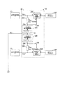
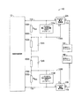
図3は、電子医療機器の患者チャネルを形成し、患者インターフェース14A及び14Bを有する2つの患者側配線11A、11Bのための過電圧保護装置又は回路30の変更された実施形態を示す。回路30は、図2の回路20と同様又は同一の構成要素を使用する。第1のバイアス抵抗22Aは、患者側配線11Aに接続された第1の端部を有し、患者側配線から延在する配線23Aの第1の一方向性の過渡電圧抑制器(TVS)24Aと直列に接続され、第1のバイアス抵抗22Aと第1の一方向性のTVS24Aとの間の接続部からMOSFET25Aのゲートに延在する配線26Bを介して接続されている。第2のバイアス抵抗22Bは、患者側配線11Bに接続された第1の端部を有し、患者側配線から延在する配線23Bを介して第2の一方向性のTVS24Bと直列に接続され、バイアス抵抗22Bと一方向性のTVS24Bとの間の接続部から患者側配線11Bに位置するMOSFET25Bのゲートに延在する配線26Bを介して接続されている。一方向性のTVSダイオード24A及び24Bは、それらの隣接する端部で、それらのカソード又はアノードのいずれかと互いに接続されている。保護回路は、電子医療機器の患者チャネル、例えばシングルチャンバペースメーカ又は血行動態モニタの1つのチャネル、又は他のタイプの医療機器に接続される。回路30は、医療機器の内部回路12が過電圧に含まれるエネルギーを吸収するリスクを回避又は低減するために、各極性の過電圧の発生時及び過電圧の発生中に2配線患者チャネルに過電圧保護を提供するように設計されている。
FIG. 3 shows a modified embodiment of an overvoltage protection device or
図4は、図3の回路30と類似するが、一方向性の電圧制限装置24A、24Bを双方向性のTVSダイオード42のような1つの双方向性の電圧制限装置に置き換えた変更された過電圧保護回路40を示す。回路の他の部分又は装置40は、図3の回路30の構成要素と同じであり、同様の部分には同様の番号が付されている。双方向性のTVSは、どちらの方向にも取り付けることができる。図3に示されているように、回路は、2つの患者側配線からなる患者チャネルに適用され、これは、シングルチャンバペースメーカ又は血行動態モニタの1つのチャネルなどであってもよい。
FIG. 4 is similar to the
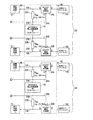
図5A及び図5Bは、デュアルチャンバペースメーカ又は2つのチャネルの血行動態モニタのような、2つの患者チャネルを有する電子医療機器に対して過電圧パルス保護を提供するように構成された変更された過電圧保護回路又は装置50の一実施形態を示す。装置50は、デュアルチャネル装置のそれぞれのチャネルに適用された図3のシングルチャネル回路30のうちの2つを備え、同様の部品には同様の参照番号が付されている。各チャネルの回路30は、一端が患者側配線11Aに接続され、配線23Aの第1の一方向性の過渡電圧抑制器(TVS)24Aと直列に接続され、抵抗22AとTVS24Aとの間の接続部からゲートMOSFET25Aのゲートに接続される第1のバイアス抵抗22Aと、一端が患者側配線11Bに接続され、配線23Bを介して第2の一方向性のTVS24Bと直列に接続され、配線26Bを介してMOSFET25Bのゲートに接続される第2のバイアス抵抗22Bとを有する。図3に示すように、一方向性のTVS装置は、カソード又はアノードのいずれかの端部と互いに接続されている。2つの回路は、ぞれぞれの回路内のTVS24Aと24Bとの間に位置するノード53(図5A)と54(図5B)との間に延在する配線52を介して接続されている。
FIGS. 5A and 5B show modified overvoltage protection configured to provide overvoltage pulse protection for an electronic medical device having two patient channels, such as a dual chamber pacemaker or a two channel hemodynamic monitor. One embodiment of a circuit or
この回路が使用される例は、デュアルチャンバペースメーカ又は血行動態モニタの2つのチャネルである。回路50は、2つのチャネルに対する過電圧保護を提供する。すなわち、回路50は、任意の患者側配線間の各極性の過電圧の発生時及び過電圧の発生中に装置を保護し、装置が過電圧に含まれるエネルギーを吸収するリスクを回避又は低減する。
An example where this circuit is used is the dual channel of a dual chamber pacemaker or hemodynamic monitor.
図6A及び6Bは、図4のものと同様の過電圧保護回路60の実施形態を示しているが、例えば、デュアルチャンバペースメーカの2つの患者チャネル又は血行力学的モニタの2つのチャネルのように、適用可能な4つの患者側配線インターフェースのそれぞれの患者側配線インターフェースに接続された各々の抵抗(インピーダンス)を使用してバイアス電圧を生成することによって、2チャネルの患者インターフェースを保護するように変更されている。
6A and 6B show an embodiment of an
この実施形態では、4つの追加の双方向性の電圧制限装置又はTVSダイオード65、66、67及び68(図6A参照)は、2つの異なるチャネルに属する患者側配線間に過渡電圧が発生した場合に回路60の電流制限能力を作動させるために、2つの患者チャネル62、64(図6B参照)のバイアス抵抗間に直列に接続される。図6Bに示すように、第1の双方向性のTVS装置65は、第1及び第2の患者チャネルの抵抗22Aの第2の端部の間の配線73に配置され、TVS装置66は、第1の患者チャネル62の抵抗22Aの第2の端部と第2の患者チャネルの抵抗22Bの第2の端部との間に接続された配線45に配置され、TVS装置67は、第1の患者チャネル内の抵抗22Bの第2の端部と、第2の患者チャネル内の抵抗22Aの第2の端部との間に接続された配線46内に配置され、TVS装置68は、第1の患者チャネル内の抵抗22Bの第2の端部と第2の患者チャネル内の抵抗22Bの第2の端部との間に接続された配線47に配置される。これにより、任意のペアを形成している患者側配線間のいずれかの極性の過電圧から医療機器を保護する。したがって、この実施形態は、一方向性のTVSを使用する前の実施形態よりも、さらに2つのTVS装置を必要とする(図5A、5B参照)。
In this embodiment, four additional bidirectional voltage limiting devices or
図7Aから図7Cは、図5A及び5Bと同様の過電圧保護回路70の実施形態を示しているが、トリプルチャンバ又は両心室ペースメーカの3つの患者チャネルのように、3つの患者チャネルを保護するように変更されている。図7Aから図7Cの回路70は、図3、図5A、図5Bの3つの過電圧保護回路30を有し、図5Bのような2つのチャネルではなく、3つの患者チャネル72、74、76を有する医療装置の3チャネルの患者インターフェースに適用され、同様の部分には同様の番号が付されている。回路70は、図5A及び図5Bに関連して上述したのと同じ方法で、6つの患者側配線インターフェースの各患者側配線インターフェースに接続された第1の端部を有するそれぞれのバイアス抵抗(インピーダンス)22A又は22Bを使用してバイアス電圧を生成するように設計される。図5A及び図5Bのように、この回路は一方向性のTVSを使用する。
7A-7C illustrate an embodiment of an
図5A、図5Bのように、一方向性のTVS24A、24Bのそれぞれのペアは、それらのカソード又はアノードのいずれかの端部で互いに接続されている。異なるチャネルの各TVSペアの間の接続部は、異なる患者チャネルに属する患者側配線間に過渡電圧が発生した場合に電流制限能力を提供するために、図7Aから図7Cに示すように配線77、78を介して互いに接続される。過電圧保護回路70は、3つのチャネルに対する過電圧保護を提供する。すなわち、過電圧保護回路70は、任意の患者側配線間の各極性の過電圧の発生時及び過電圧の発生中に装置を保護し、装置が過電圧に含まれるエネルギーを吸収するリスクを低減又は排除する。
As in FIGS. 5A and 5B, each pair of
図8Aから図8Dは、図6A及び図6Bと同様の過電圧保護回路80の実施形態を示しているが、3チャネルの患者インターフェースを保護するように変更されており、同様の部品には同様の参照番号が使用されている。上述の実施形態と同様に、回路80は、患者側配線インターフェースに一端が接続された抵抗(インピーダンス)を使用してバイアス電圧を生成するように構成される。この場合、それぞれのバイアス抵抗は、例えば、3つの患者チャネル72(図8B)、74(図8C)、及び76(図8D)を有するトリプルチャンバペースメーカ又は血行動態モニタの3つの患者チャネルのように、適用可能なそれぞれ6つの患者側配線インターフェースに接続された第1の端部を有する。以下でより詳細に説明するように、図6A、図6Bと同様に、この回路は、異なる患者チャネルの患者側配線間に追加の双方向性のTVS装置とともに、各患者チャネルのバイアス抵抗22A、22Bの間に双方向性のTVS装置42を使用する。これにより、2つの異なるチャネルにおける患者側配線間に発生する過電圧を含む、任意のペアの患者側配線間の任意の極性の過電圧の発生時及び過電圧の発生中に過電圧保護を行う。
FIGS. 8A-8D illustrate an embodiment of an
双方向性の過渡電圧抑制回路を備えた3チャネルの過電圧保護を実現するには、各患者チャネルに1つの双方向性のTVSを適用するだけでは不十分である。図に示された実施形態では、3つの患者チャネルの間に他の12の双方向性の過渡電圧抑制装置又はTVS装置が接続され、異なる患者チャネルに属する患者側配線間に過渡電圧が発生した場合にこの保護回路の電流制限能力を作動させる。図8Aから図8Dにおいて、双方向性のTVSが各ペアの患者側配線間に接続されている。接続配線は以下の通りである。 Applying one bidirectional TVS to each patient channel is not sufficient to achieve 3-channel overvoltage protection with a bidirectional transient voltage suppression circuit. In the embodiment shown in the figure, the other 12 bidirectional transient voltage suppression devices or TVS devices are connected between the three patient channels, and a transient voltage is generated between the patient side wirings belonging to different patient channels. In some cases, the current limiting capability of this protection circuit is activated. 8A to 8D, a bidirectional TVS is connected between each pair of patient-side wires. The connection wiring is as follows.
TVS81−チャネル72のバイアス抵抗22Aとチャネル74のバイアス抵抗22Aとの間(Jを介して図8B及び図8C参照)。
TVS81—between the
TVS82−チャネル74のバイアス抵抗22Aとチャネル76のバイアス抵抗22Bとの間(Jを介して図8C及び図8Dを参照)。
TVS82—between
TVS83−チャネル72のバイアス抵抗22Aとチャネル76のバイアス抵抗22Aとの間(I、Hを介して図8B、図8C、図8D参照)。
Between the
TVS84−チャネル72のバイアス抵抗22Aとチャネル74のバイアス抵抗22Bとの間(A、Dを介して図8B、図8A、図8C参照)。
TVS84-between the
TVS85−チャネル74のバイアス抵抗22Bとチャネル76のバイアス抵抗22Aとの間(D、E、Hを介して図8C、図8A、図8D参照)。
TVS85—between the
TVS86−チャネル72のバイアス抵抗22Aとチャネル76のバイアス抵抗22Bとの間(A、F、Gを介して図8B、図8A、図8D参照)。
TVS86—between the
TVS87−チャネル72のバイアス抵抗22Bとチャネル74のバイアス抵抗22Aとの間(B、Cを介して図8B、図8A、図8C参照)。
TVS87-between the
TVS88−チャネル74のバイアス抵抗22Aとチャネル76のバイアス抵抗22Aとの間(C、E、Hを介して図8C、図8A、図8D参照)。
TVS88-between the
TVS89−チャネル72のバイアス抵抗22Bとチャネル74のバイアス抵抗22Bとの間(B、Dを介して図8B、図8A、図8C参照)。
TVS89-between the
TVS91−チャネル74のバイアス抵抗22Bとチャネル76のバイアス抵抗22Bとの間(D、F、Gを介して図8C、図8A、図8D参照)。
TVS91—between the
TVS92−チャネル72のバイアス抵抗22Bとチャネル76のバイアス抵抗22Aとの間(B、E、Hを介して図8B、図8A、図8D参照)。
TVS92—between the
TVS93−チャネル72のバイアス抵抗22Bとチャネル76のバイアス抵抗22Bとの間(B、F、Gを介して図8B、図8A、図8D参照)。
TVS93—between the
回路80における双方向性の過渡電圧抑制器(TVS)の総数は15である。これは、一方向性のTVSを使用する図7Aから図7Cの実施形態よりもはるかに多く、一方向性のTVSが6つだけ必要である。しかし、TVS装置は大きな電流を流す必要がなく、高出力装置である必要はないので、いくつかの実施形態では、小型の最新のESD保護TVS装置を使用することができる。これらの装置は、ほぼすべて双方向性であるため、10個の電子部品を追加しても装置のサイズや経費は大幅に増加しない。
The total number of bidirectional transient voltage suppressors (TVS) in
図9Aから図9Dは、それぞれの配線インターフェースから延在するそれぞれの配線を介して6つの患者側配線インターフェース用の患者側配線インターフェースに接続された第1の端部を有する抵抗(インピーダンス)を使用してバイアス電圧を生成し、各患者チャネルのバイアス抵抗間に双方向性のTVSを使用する過電圧保護回路90の簡略化された実施形態を示す。上述の2つの実施形態と同様に、この実施形態は、例えば、トリプルチャンバペースメーカの3つの患者チャネルに適用可能である。
9A through 9D use resistors (impedances) having first ends connected to patient-side wiring interfaces for six patient-side wiring interfaces via respective wires extending from the respective wiring interfaces. 6 illustrates a simplified embodiment of an
図4、図6A、図6Bに示すように、回路90は、3つの過電圧保護回路40を有し、図6A、図6Bのように2つのチャネルではなく3つの患者チャネル72、74、76を有する医療機器の3チャネル患者インターフェースに適用され、同様の部分には同様の番号が付されている。回路90は、図8Aから図8Dと同様であるが、単純化された双方向性のTVS構成を有する3チャネルの患者インターフェースを提供する。この回路を使用できる例は、二心室ペースメーカである。回路90は、3つのチャネルに対して完全な過電圧保護を行う。すなわち、回路90は、6つの患者側配線のいずれかの間の各極性の過電圧の発生時及び過電圧の発生中に装置を保護する。図8Aから図8Dのように、各患者チャネル72、74、76には、1つの双方向性の過渡電圧抑制器42が装備されている。しかしながら、図8Aから図8Dのように12個の双方向性のTVS素子の代わりに、患者チャネル間には6個の双方向性のTVS素子95、96しかない。これは、不均一なTVSブレークダウン電圧を使って行われる。電圧過渡が予想される患者側配線の組み合わせによっては、ブレークダウン電圧UTVSが予想されるが、他の患者側配線の組み合わせではブレークダウン電圧が2UTVSに等しくなる。しかしながら、これは、UTVSが発生する可能性のある過渡電圧のほんの一部である多くの場合において、保護回路の保護能力を提供する際には問題ではない。図9Aから図9Dにおいて、各双方向性のTVS95は、各ペアの回路40(E、G、I参照)のバイアスダイオード22Aの間に接続され、各双方向性のTVS96が、各ペアの回路40(F、H、J参照)のバイアスダイオード22Bの間に接続され、合計6つの双方向性のTVS装置を構成する。しかしながら、図8Aから図8Dとは異なり、1つの回路のバイアスダイオード22Aと他の2つの回路のいずれかのバイアスダイオード22Bとの間には双方向性のTVS素子はなく、図8Aから図8Dの双方向性のTVS素子のうちの6つは省略されている。
As shown in FIGS. 4, 6A, and 6B, the
図8から図8D又は図9Aから図9Dのように、図7Aから図9Dの3チャネル過電圧保護回路は、図7Aから図9Dのチャネル72、74、76と同様の方法で、4つ目のチャネル用の追加の回路30又は40と、2つの一方向性のTVS装置ではなく双方向性のTVSがバイアス抵抗間で使用される場合に、各チャネルの患者側配線間に追加の双方向性のTVS装置とを追加することによって、心臓の4つの部屋の心臓モニタ又はペースメーカのような4チャネルの医療装置に対してスケールアップすることができる。
As shown in FIGS. 8 to 8D or 9A to 9D, the 3-channel overvoltage protection circuit of FIGS. 7A to 9D is similar to the
図10は、2つの患者側配線インターフェース又は1つの患者医療チャネルの過電圧保護回路100の他の実施形態を示す。回路100は、装置内部回路12と医療機器の患者インターフェースとの間に接続されている。図10に示すように、この実施形態では、過渡電圧抑制器又はTVS素子は、それぞれの補償コンデンサ104A、104Bと並列にそれぞれ抵抗102A、102Bで置換され、Aの一端がそれぞれ患者側配線11A又は11Bに接続されたバイアス抵抗105A又は105Bと直列に接続されている。いくつかの実施形態では、補償コンデンサ104A及び104Bを省略することができる。上述した実施例と同様に、各患者側配線11A、11Bは、MOSFET電流制限器25A、25Bを有する。抵抗105Aと抵抗102Aとの間の接続部106Aは、配線108Aを介して、MOSFET25Aのゲートに接続されている。同様に、接続部106Bは、配線108Bを介して、MOSFET25Bのゲートに接続されている。それぞれ一方向性の電圧制限装置又はTVSダイオード110A、110Bは、患者側配線11A、11Bと配線108A、108Bとの間のそれぞれバイアス抵抗105A、105Bと並列に接続されている。一方向性の電圧制限装置110Aは、患者側配線11Aに接続された陽極と、接続部106Aに接続された陰極とに接続され、一方向性の電圧制限装置110Bは、患者側配線11Bに接続された陽極と接続部106Bに接続された陰極とに接続されている。
FIG. 10 illustrates another embodiment of an
過電圧保護回路100は、1つの患者チャネルを構成する2つの患者側配線11A、11Bを保護し、図2から図9Dに示される上述の実施形態と全く同じ方法で使用される電流制限装置25A、25B(デプリーション型MOSFETなどで構築される)を利用する。しかしながら、この実施形態では、バイアス電圧は、抵抗105A及び102Aを含む第1の抵抗分圧器と、2つの患者側配線間に構築された抵抗105B及び102Bを備える第2の抵抗分圧器から得られる。第1の過電圧のランプが発生すると、最初は小さな電流が分圧器の抵抗を通って流れる。バイアス抵抗105A又は105Bの一方の両端の電圧がMOSFETの必要バイアスレベルに達すると、それぞれのMOSFETは患者側配線を流れる電流を遮断する。どのMOSFETが最初にオフになるかは、過渡過電圧の方向に依存する。分圧器は、MOSFETの遮断が図2から図9Dの過電圧保護回路の場合よりもさらに迅速に行われるように調整することができる。一例では、抵抗105A及び105Bはそれぞれ10キロオームの抵抗を有し、抵抗102A及び102Bはそれぞれ22キロオームの抵抗を有し、コンデンサ104A及び104Bはそれぞれ10ナノファラドの静電容量を有する。抵抗105A及び105Bの抵抗は、10キロオームから1メガオームの範囲内であり得るが、抵抗102A及び102Bの適切な抵抗の範囲は、22キロオームから3.3メガオームである。補償キャパシタ104A及び104Bは、数ピコファラドから22ナノファラドの容量を有することができる。実際の値は、過電圧保護回路が使用される装置の患者側配線の特性に強く依存する。
The
分圧器は、各抵抗対105A、102A及び105B、102Bを流れる電流が非常に小さくなるように、高オーム抵抗で構成することができる。しかしながら、分圧器の大きさを決定する手順(dimensioning procedure)の間に、バイアス容量105A又は105Bとともにこの容量がローパスフィルタを形成するので、MOSFETゲート端子Gに見られるMOSFET容量Cissに関して注意する必要がある。Cissはゲート−ソース間容量とゲート−ドレイン間容量(Ciss=Cgs+Cgd)の和である。回路に使用される特定のMOSFETに依存して、この容量は、数ナノファラッドまでの値を有することができる。これを補償するために、それぞれの補償コンデンサ104A、104Bがそれぞれの抵抗102A、102Bと並列に印加される。いくつかの実施形態では、正確な補償の場合よりも過渡過電圧に対する応答が速くなるので、補償コンデンサをCissに対して過補償するように配置することが最良な配置であり得る。しかしながら、コンデンサ104A、104Bの導入は、保護回路の周波数応答に影響を及ぼす。図10の実施形態で使用された上述の例の構成要素パラメータでは、約25キロヘルツで−3デシベルの減衰限界が達成される。このような周波数応答は、過電圧保護装置がペースメーカ装置又はECGモニタに使用されるとき、ほとんどの生体信号に対して十分である。血行動態モニタの保護のための実施形態では、回路がより少ない減衰を導入するように、回路パラメータを変更することができる。電圧測定を担当する血行動態モニタの患者チャネルの場合、補償コンデンサの値をピコファラド値に減らすか、補償コンデンサを完全に省略することができる。電圧測定患者チャネルがペースメーカチャネル又は血行動態モニタの電流チャネルほど低いインピーダンスを示さないため、これは可能である。
The voltage divider can be configured with a high ohm resistance so that the current through each
回路100は、ゲート端子とソース端子との間の過大な電圧から保護するために、各MOSFET電流制限器25A、25Bのゲート端子とソース端子の間に接続されたTVS素子110A及び110Bを有する。しかしながら、この回路で使用されるTVS素子は、患者側配線に電圧制限能力を導入しないことに留意すべきである。回路100内のTVS素子の唯一の目的は、MOSFET電流制限器を過度のゲート−ソース電圧から保護して、MOSFETを損傷させることである。上述したように、過電圧保護回路100の電圧制限は、MOSFET25A及び25Bの遮断によって単独で達成される。所望の遮断効果は、上述した分圧器の適切な大きさに強く依存する。
The
図10に示す過電圧保護回路には、図2及び図3から図9Dに示す回路に比べて2つの利点がある。第1の利点は、過電圧過渡現象に対してより感度が高いこと、第2の利点は、より良好に制御が可能であり、MOSFETの遮断がより深いことである。これは、過渡事象によってもたらされるエネルギーをより良く排除し、改善されたエネルギー排除能力をもたらす。しかしながら、この実施形態における過電圧保護は、上述の実施形態よりも正確な大きさ又は構成要素パラメータに依存する。大きさは、過電圧保護回路が適用される特定の医療機器によって大きく左右される。 The overvoltage protection circuit shown in FIG. 10 has two advantages over the circuits shown in FIGS. 2 and 3 to 9D. The first advantage is that it is more sensitive to overvoltage transients, and the second advantage is that it can be better controlled and has a deeper MOSFET cutoff. This better eliminates the energy provided by the transient event, resulting in improved energy rejection capability. However, overvoltage protection in this embodiment relies on more accurate magnitude or component parameters than the above-described embodiment. The magnitude depends greatly on the specific medical device to which the overvoltage protection circuit is applied.
図11A及び図11Bは、例えば、デュアルチャンバペースメーカ又は2チャネルの血行動態モニタのように、2つの患者チャネル118(図11A)及び119(図11B)を有する電子医療機器の過電圧保護を提供するために、図10と同じ過電圧保護技術を使用する変更された過電圧保護回路又は装置112の一実施形態を示す。装置120は、デュアルチャネル装置のそれぞれのチャネル118、119に適用された図10の1つのチャネル回路100のうちの2つを有し、同様の部品には同様の参照番号が付される。図10のように、各チャネルの回路100は、一端が患者側配線11Aに接続され、補償コンデンサ104Aと並列に接続された第1の抵抗102Aと直列に接続された第1のバイアス抵抗105Aとを有する。抵抗102Aと105Aとの間の接続部106Aは、配線108Aを介して患者側配線11AのMOSFET25Aのゲートに接続されている。それぞれ第2のバイアス抵抗105Bは、一端が患者側配線11Bに接続され、補償コンデンサ104Bと並列に接続された第2の抵抗102Bと直列に接続されている。抵抗102Bと105Bとの間の接続部106Bは、配線108Bを介して、患者側配線11Bに位置するMOSFET25Bのゲートに接続されている。さらに、各回路内の電圧制限装置102Aと102Bとの間の接続部115は、配線116によって互いに接続されている。
FIGS. 11A and 11B provide overvoltage protection for an electronic medical device having two patient channels 118 (FIG. 11A) and 119 (FIG. 11B), for example, a dual chamber pacemaker or a two-channel hemodynamic monitor. Figure 1 illustrates one embodiment of a modified overvoltage protection circuit or
回路112が使用される医療機器の例は、デュアルチャンバペースメーカ又は2つのチャネルの血行動態モニタである。回路112は、2つのチャネルに対する過電圧保護を提供する。すなわち、回路112は、任意の患者側配線間で各極性の過電圧の発生時及び過電圧の発生中に医療装置を保護し、装置が過電圧に含まれるエネルギーを吸収するリスクを低減又は排除する。
Examples of medical devices in which
2チャネル過電圧保護回路112の一例では、抵抗105A及び105Bの抵抗はそれぞれ470キロオームであり、抵抗102A及び102Bの抵抗はそれぞれ1.5メガオームであり、コンデンサ104A及び104Bの容量は10ナノファラドである。
In an example of the two-channel
図12Aから図12Cは、図1及び図2と同様の変更された過電圧保護回路又は装置120の一実施形態を示し、トリプルチャンバペースメーカ又は3つのチャネルを有する血行力学的モニタのように、3つの患者チャネル122(図12A)、124(図12B)、125(図12C)を有する電子医療機器の過電圧パルス保護を提供するように構成される。装置120は、3チャネル装置のそれぞれのチャネル122、124、125に適用された図10の1つのチャネル回路100のうちの3つを備え、同様の部品には同様の参照番号が付されている。図10のように、各チャネルの回路100は、一端が配線11Aに接続され、補償コンデンサ104Aと並列に接続された第1の抵抗102Aと直列に接続された第1のバイアス抵抗105Aとを有する。抵抗102Aと105Aとの間の接続部106Aは、配線108Aを介して患者側配線11AのMOSFET25Aのゲートに接続されている。TVSダイオード110Aは、バイアス抵抗105Aと並列に、配線11Aと108Aとの間に接続されている。それぞれの第2バイアス抵抗105Bは、一端で患者側配線11Bに接続され、補償コンデンサ104Bと並列に接続された第2抵抗102Bと直列に接続されている。抵抗102Bと105Bとの間の接続部106Bは、配線108Bを介して患者側配線11Bに位置するMOSFET25Bのゲートに接続されている。TVSダイオード110Bは、バイアス抵抗105Bと並列に、配線11Bと108Bとの間に接続されている。さらに、各回路内の電圧制限装置102Aと102Bとの間の接続部115は、配線116と126によって互いに接続されている。
FIGS. 12A-12C illustrate one embodiment of a modified overvoltage protection circuit or
図1及び図2の変更された過電圧保護回路120は、図12Aから図12Cは、6つの患者側配線11A、11Bのそれぞれ患者側配線にそれぞれの一端が接続された抵抗(インピーダンス)をそれぞれ使用してバイアス電圧を生成することによって、3チャネルの患者インターフェースを保護するように設計されている。この装置は、例えば、トリプルチャンバペースメーカ又は血行動態モニタの3つの患者チャネルに適用可能である。3チャネル過電圧保護回路120の一例では、抵抗105A及び105Bの抵抗はそれぞれ470キロオームであり、抵抗102A及び102Bの抵抗はそれぞれ1.5メガオームであり、コンデンサ104A及び104Bの容量は10ナノファラドである。
The modified
上記の過電圧保護回路及び方法は、電気又は電子医療機器の過電圧保護を提供するものとして記載されているが、代わりに、2つの端子間の偶発的な過電圧から他のタイプの回路を保護するために使用されてもよい。いくつかの実施形態では、過電圧保護回路は、医療機器の内部回路自体に組み込まれてもよく、既存の医療機器の患者出力/入力端子又はチャネルに接続されるように設けられてもよい。上述の過電圧保護回路は、(人間又は動物の)体内又は体表の治療又はモニタリングの目的で使用される任意の電子医療機器と併用することができる。 Although the above overvoltage protection circuits and methods have been described as providing overvoltage protection for electrical or electronic medical devices, instead to protect other types of circuits from accidental overvoltages between two terminals. May be used. In some embodiments, the overvoltage protection circuit may be integrated into the internal circuit itself of the medical device or may be provided to be connected to a patient output / input terminal or channel of an existing medical device. The overvoltage protection circuit described above can be used in conjunction with any electronic medical device that is used for the purpose of treatment or monitoring of the body or body surface (human or animal).
開示された実施形態に係る上記の説明は、当業者が本発明を実施又は使用することを可能にするために提供される。これらの実施形態に対する様々な変更は、当業者には容易に明らかであり、本明細書に記載された一般的な原理は、本発明の精神又は範囲から逸脱することなく他の実施形態に適用することができる。したがって、本明細書に提示される説明及び図面は、本発明の現時点で好ましい実施形態を表しており、それゆえ、本発明によって広く企図される主題を代表することが理解されるべきである。本発明の範囲は、当業者に明らかになる可能性のある他の実施形態を完全に包含し、添付の請求項以外になんら限定されるものではないことがさらに理解される。 The above description of the disclosed embodiments is provided to enable any person skilled in the art to make or use the present invention. Various modifications to these embodiments will be readily apparent to those skilled in the art, and the generic principles described herein may be applied to other embodiments without departing from the spirit or scope of the invention. can do. Accordingly, it is to be understood that the description and drawings presented herein represent presently preferred embodiments of the present invention and therefore represent subject matter that is broadly contemplated by the present invention. It is further understood that the scope of the present invention fully encompasses other embodiments that may be apparent to those skilled in the art and is not limited in any way other than the appended claims.
Claims (15)
前記第1の端部と前記第2の端部との間の前記第1の配線に接続された電流制限装置であって、前記電流制限装置はオン状態とオフ状態とを有し、前記オフ状態のときに通過する電流を前記第1の端部と前記第2の端部との間に制限し、所定のバイアス電圧に応答して前記オン状態から前記オフ状態に切り替わるように構成された前記電流制限装置と、
前記第1の配線から延在する第2の配線と、
前記第2の配線に接続され、少なくとも1つのバイアス素子と、少なくとも1つのバイアス電圧生成装置と直列に接続された追加の回路素子とを有するバイアス電圧生成回路と、
前記第1の配線の過渡過電圧に応答して前記電流制限装置に前記所定のバイアス電圧を印加するように構成された前記バイアス素子と前記追加の回路素子と、
を有し、
前記電流制限装置は、スイッチオフされ、前記第1の配線を流れる電流を制限する、過電圧保護装置。 A first wiring connecting the first end and the second end;
A current limiting device connected to the first wiring between the first end and the second end, wherein the current limiting device has an on state and an off state, and the off A current passing through the state is limited between the first end and the second end, and is configured to switch from the on state to the off state in response to a predetermined bias voltage. The current limiting device;
A second wiring extending from the first wiring;
A bias voltage generating circuit connected to the second wiring and having at least one bias element and an additional circuit element connected in series with the at least one bias voltage generating device;
The bias element and the additional circuit element configured to apply the predetermined bias voltage to the current limiting device in response to a transient overvoltage of the first wiring;
Have
The overcurrent protection device, wherein the current limiting device is switched off and limits a current flowing through the first wiring.
及び/又は、
前記追加の回路素子は、第1のバイアス抵抗と第2のバイアス抵抗との間に接続された少なくとも1つの電圧制限装置を有し、
及び/又は、
前記電流制限装置は、第1のデプリーション型金属酸化物半導体電界効果トランジスタ(MOSFET)と第2のデプリーション型金属酸化物半導体電界効果トランジスタ(MOSFET)とを有する、請求項2に記載の過電圧保護装置。 Each bias resistor has a resistance in the range of 50 ohms to 1 kilohm,
And / or
The additional circuit element includes at least one voltage limiting device connected between a first bias resistor and a second bias resistor;
And / or
3. The overvoltage protection device according to claim 2, wherein the current limiting device includes a first depletion type metal oxide semiconductor field effect transistor (MOSFET) and a second depletion type metal oxide semiconductor field effect transistor (MOSFET). .
及び/又は、
前記電圧制限装置は、前記第1のバイアス抵抗の前記第2の端部に接続された第1の一方向性のTVSと、前記第1の一方向性のTVSと前記第2のバイアス抵抗の前記第2の端部との間に接続された第2の一方向性のTVSと、を有する、請求項3に記載の過電圧保護装置。 At least one of the voltage limiting devices comprises a transient voltage suppressor (TVS);
And / or
The voltage limiting device includes: a first unidirectional TVS connected to the second end of the first bias resistor; the first unidirectional TVS; and the second bias resistor. The overvoltage protection device according to claim 3, further comprising: a second unidirectional TVS connected between the second end portion.
第2の端子に接続されるドレイン端子と、
前記医療機器の前記内部回路に接続されるソース端子と、
ゲート端子と、
を有し、
前記第1のバイアス抵抗は、第1のMOSFETの前記ゲート端子に接続され、
前記第2のバイアス抵抗は、第2のMOSFETの前記ゲート端子に接続される、請求項3又は請求項4に記載の過電圧保護装置。 Each MOSFET is
A drain terminal connected to the second terminal;
A source terminal connected to the internal circuit of the medical device;
A gate terminal;
Have
The first bias resistor is connected to the gate terminal of the first MOSFET;
The overvoltage protection device according to claim 3 or 4, wherein the second bias resistor is connected to the gate terminal of a second MOSFET.
第1のバイアス抵抗と直列に接続されて第1の分圧器を形成する第1の抵抗と、
第2のバイアス抵抗と直列に接続されて第2の分圧器を形成する第2の抵抗と、
第1の電流制限装置に接続された前記第1のバイアス抵抗と前記第1の抵抗との間の第1の接続部と、
第2の電流制限装置に接続された前記第2のバイアス抵抗と前記第2の抵抗との間の第2の接続部と、を有する、請求項2乃至請求項5のいずれか1項に記載の過電圧保護装置。 At least one of the additional circuit elements is
A first resistor connected in series with a first bias resistor to form a first voltage divider;
A second resistor connected in series with a second bias resistor to form a second voltage divider;
A first connection between the first bias resistor and the first resistor connected to a first current limiting device;
6. The device according to claim 2, further comprising: a second connection portion between the second bias resistor and the second resistor connected to a second current limiting device. 7. Overvoltage protection device.
前記医療機器の前記内部回路と通信するそれぞれの前記第1の端部と、
それぞれ第1の患者インターフェースと第2の患者インターフェースと、前記第2の患者チャネルの前記第1の患者側配線と前記第2の患者側配線とにそれぞれ第1の電流制限装置と第2の電流制限装置とを有する前記第2の端部と、
前記第2の患者チャネルの前記第1の患者側配線と前記第2の患者側配線との間に延在する前記第2の配線に接続された第1のバイアス電圧生成回路と同一であり、前記第2の患者チャネルのそれぞれ前記第1の患者側配線又は前記第2の患者側配線に過渡電圧パルスが発生した場合に、前記第2の患者チャネルの少なくともそれぞれ前記第1の電流制限装置又は前記第2の電流制限装置をオフにするバイアス電圧を生成するように構成される第2のバイアス電圧生成回路と、をさらに有し、
及び/又は、
前記第1の患者チャネルと前記第2の患者チャネルとの前記バイアス電圧生成回路の第1のバイアス素子と第2のバイアス素子とはバイアス抵抗を有し、
前記追加の回路素子は前記バイアス抵抗の間に接続された少なくとも1つの電圧制限装置を有する、請求項2乃至請求項6のいずれか1項に記載の過電圧保護装置。 A second patient channel having the first patient-side wiring and the second patient-side wiring; and the first end and the second end on opposite sides;
Each of the first ends in communication with the internal circuit of the medical device;
A first current limiting device and a second current respectively for the first patient interface and the second patient interface, and for the first patient side wiring and the second patient side wiring of the second patient channel, respectively. Said second end having a restriction device;
The same as a first bias voltage generating circuit connected to the second wiring extending between the first patient-side wiring and the second patient-side wiring of the second patient channel; When a transient voltage pulse occurs in each of the first patient-side wiring or the second patient-side wiring of each of the second patient channels, at least each of the first current limiting devices of the second patient channels or A second bias voltage generation circuit configured to generate a bias voltage to turn off the second current limiting device;
And / or
The first bias element and the second bias element of the bias voltage generation circuit of the first patient channel and the second patient channel have a bias resistor,
The overvoltage protection device according to any one of claims 2 to 6, wherein the additional circuit element has at least one voltage limiting device connected between the bias resistors.
接続配線は、前記第1の患者チャネルの前記第1の一方向性の電圧制限装置と前記第2の一方向性の電圧制限装置との間の第1の位置で接続された前記第1の端部と、前記第2の患者チャネルの前記第1の一方向性の電圧制限装置と前記第2の一方向性の電圧制限装置との間の第2の位置で接続された前記第2の端部と、を有し、
及び/又は、
それぞれの前記患者チャネルの前記追加の回路素子は、それぞれの前記患者チャネルの前記バイアス抵抗の間に接続された第1の双方向性の電圧制限装置を有し、それぞれの前記患者チャネルの第1の接続部と第2の接続部とは、第1のバイアス抵抗と双方向性の電圧制限装置との間と、第2のバイアス抵抗と双方向性の電圧制限装置との間とにそれぞれ配置され、
第1の電流経路は、前記第1の患者チャネルの前記第1の接続部と前記第2の患者チャネルの前記第2の接続部との間に延在し、第2の双方向性の電圧制限装置が前記第1の電流経路に配置され、
第2の電流経路は、前記第1の患者チャネルの前記第1の接続部と前記第2の患者チャネルの前記第1の接続部との間に延在し、第3の双方向性の電圧制限装置が前記第2の電流経路に配置され、
第3の電流経路は、前記第1の患者チャネルの前記第2の接続部と前記第2の患者チャネルの前記第1の接続部との間に延在し、第4の双方向性の電圧制限装置が前記第3の電流経路に配置され、
第4の電流経路は、前記第1の患者チャネルの前記第2の接続部と前記第2の患者チャネルの前記第2の接続部との間に延在し、第5の双方向性の電圧制限装置が前記第4の電流経路に配置される、請求項7に記載の過電圧保護装置。 At least one of the additional circuit elements includes a first unidirectional voltage limiting device and a second unidirectional voltage limiting device connected between the bias resistors of each patient channel;
A connecting wire is connected at a first location between the first unidirectional voltage limiting device and the second unidirectional voltage limiting device of the first patient channel. The second connected at an end and a second location between the first unidirectional voltage limiting device and the second unidirectional voltage limiting device of the second patient channel. An end, and
And / or
The additional circuit element of each patient channel has a first bidirectional voltage limiting device connected between the bias resistors of the respective patient channel, the first of the respective patient channel The second connection portion and the second connection portion are respectively disposed between the first bias resistor and the bidirectional voltage limiting device and between the second bias resistor and the bidirectional voltage limiting device. And
A first current path extends between the first connection of the first patient channel and the second connection of the second patient channel, and a second bidirectional voltage A limiting device is disposed in the first current path;
A second current path extends between the first connection of the first patient channel and the first connection of the second patient channel, and a third bidirectional voltage A limiting device is disposed in the second current path;
A third current path extends between the second connection of the first patient channel and the first connection of the second patient channel, and a fourth bidirectional voltage A limiting device is disposed in the third current path;
A fourth current path extends between the second connection of the first patient channel and the second connection of the second patient channel, and a fifth bidirectional voltage The overvoltage protection device according to claim 7, wherein a limiting device is arranged in the fourth current path.
前記医療機器の前記内部回路と通信するそれぞれの前記第1の端部と、
それぞれ前記第1の患者インターフェースと前記第2の患者インターフェースと、前記第3の患者チャネルの前記第1の患者側配線と前記第2の患者側配線とにそれぞれ前記第1の電流制限装置と前記第2の電流制限装置とを有する前記第2の端部と、
前記第2の患者チャネルの前記第1のバイアス電圧生成回路と前記第2のバイアス電圧生成回路と同一であり、前記第3の患者チャネルのそれぞれ前記第1の患者側配線又は前記第2の患者側配線に過渡電圧パルスが発生した場合に、前記第3の患者チャネルの少なくともそれぞれ前記第1の電流制限装置又は前記第2の電流制限装置をオフにするバイアス電圧を生成するように構成される第3のバイアス電圧生成回路と、をさらに有する、請求項7又は請求項8に記載の過電圧保護装置。 A third patient channel having the first patient-side wiring, the second patient-side wiring, and the first and second ends on opposite sides;
Each of the first ends in communication with the internal circuit of the medical device;
The first current limiting device and the second patient interface, respectively, and the first patient side wiring and the second patient side wiring of the third patient channel, respectively. Said second end having a second current limiting device;
Same as the first bias voltage generation circuit and the second bias voltage generation circuit of the second patient channel, and the first patient side wiring or the second patient of the third patient channel, respectively. Configured to generate a bias voltage to turn off at least the first current limiter or the second current limiter, respectively, of the third patient channel when a transient voltage pulse occurs on a side wire The overvoltage protection device according to claim 7, further comprising a third bias voltage generation circuit.
少なくとも1つの前記追加の回路素子は、前記第1のバイアス抵抗と直列に接続された第1の抵抗と、前記第2のバイアス抵抗並びに第1の分圧器と第2の分圧器とを形成する前記第1の抵抗と直列に接続される第2の抵抗と、前記第1の電流制限装置に接続された前記第1の分圧器の抵抗の間の接続部と、前記第2の電流制限装置に接続された前記第2の分圧器の抵抗との間の接続部と、を有し、
少なくとも1つの接続配線は、前記第1の患者チャネルの前記第1の抵抗と前記第2の抵抗との間に接続された前記第1の端部と、前記第2の患者チャネルの前記第1の抵抗と前記第2の抵抗との間に接続された前記第2の端部とを有する、請求項7乃至請求項9のいずれか1項に記載の過電圧保護装置。 The first bias element and the second bias element of the bias voltage generation circuit for the first patient channel and the second patient channel include a first bias resistor and a second bias resistor, respectively. Have
At least one of the additional circuit elements forms a first resistor connected in series with the first bias resistor, the second bias resistor, and a first voltage divider and a second voltage divider. A connection between a second resistor connected in series with the first resistor and a resistor of the first voltage divider connected to the first current limiting device; and the second current limiting device. A connection between the resistor of the second voltage divider connected to
At least one connection line is connected to the first end of the first patient channel and the first end of the second patient channel connected between the first resistance and the second resistance. The overvoltage protection device according to any one of claims 7 to 9, further comprising: a second resistor connected between the second resistor and the second resistor.
医療機器の電子部品の間で電気信号を伝える第1の患者側配線と第2の患者側配線とを有し、前記第1の患者側配線と前記第2の患者側配線とにそれぞれ接続される第1の患者インターフェースと第2の患者インターフェースとを有する少なくとも1つの患者チャネルと、
を有し、
前記患者チャネルに関連付けられ、前記第1の患者側配線に配置された第1の電流制限装置と、前記第2の患者側配線に配置された第2の電流制限装置と、前記第1の患者側配線と前記第2の患者側配線との外側にそれぞれ配置された第1のバイアス電圧生成装置と第2のバイアス電圧生成装置とを有し、第1の配線と第2の配線との過渡電圧に応答して、前記第1の配線又は前記第2の配線を流れる電流を制限するために、それぞれ前記第1の電流制限装置又は前記第2の電流制限装置をオフにし、所定のバイアス電圧を生成するように構成される過電圧保護回路と、を有する医療機器。 One or more electronic components;
A first patient-side wiring and a second patient-side wiring for transmitting an electrical signal between electronic components of the medical device are connected to the first patient-side wiring and the second patient-side wiring, respectively. At least one patient channel having a first patient interface and a second patient interface;
Have
A first current limiting device associated with the patient channel and disposed on the first patient side wiring; a second current limiting device disposed on the second patient side wiring; and the first patient A first bias voltage generation device and a second bias voltage generation device respectively disposed on the outer side of the side wiring and the second patient side wiring, and transients between the first wiring and the second wiring In response to a voltage, in order to limit the current flowing through the first wiring or the second wiring, the first current limiting device or the second current limiting device is turned off, respectively, and a predetermined bias voltage An overvoltage protection circuit configured to generate a medical device.
及び/又は、
少なくとも1つの前記電圧制限装置は、前記第1のバイアス抵抗と前記第2のバイアス抵抗との間に直列に接続された第1の一方向性の電圧制限装置と第2の一方向性の電圧制限装置とを有し、
及び/又は、
少なくとも1つの前記電圧制限装置は、前記第1のバイアス抵抗と前記第2のバイアス抵抗との間に接続された1つの双方向性の電圧制限装置を有し、
及び/又は、
少なくとも1つの前記電圧制限装置は、第1の分圧器を形成するために前記第2のバイアス抵抗に接続された第1の抵抗と、前記第1の分圧器と直列に接続された前記第2のバイアス抵抗に接続され、第2の分圧器を形成する第2の抵抗と、を有する、請求項11に記載の医療機器。 Each of the first voltage generation device and the second voltage generation device has a first end connected to the first patient-side wiring and the second patient-side wiring, respectively. A bias resistor, a second bias resistor, and at least one voltage limiting device connected between the first bias resistor and the second bias resistor, respectively, for controlling a bias voltage; ,
And / or
At least one of the voltage limiting devices includes a first unidirectional voltage limiting device and a second unidirectional voltage connected in series between the first bias resistor and the second bias resistor. A limiting device,
And / or
At least one of the voltage limiting devices comprises one bidirectional voltage limiting device connected between the first bias resistor and the second bias resistor;
And / or
At least one of the voltage limiting devices includes a first resistor connected to the second bias resistor to form a first voltage divider and the second resistor connected in series with the first voltage divider. And a second resistor connected to the bias resistor and forming a second voltage divider.
及び/又は、
前記第1の抵抗と並列に接続された第1のコンデンサと、前記第2の抵抗と並列に接続された第2のコンデンサと、をさらに有する、請求項12に記載の医療機器。 The first bias resistor and the second bias resistor each have a resistance in a range of 10 kilohms to 1 megaohm, and the first resistor and the second resistor are each in a range of 22 kilohms to 3.3 kilohms. Has a resistance of mega-ohms,
And / or
The medical device according to claim 12, further comprising: a first capacitor connected in parallel with the first resistor; and a second capacitor connected in parallel with the second resistor.
前記患者インターフェースと医療機器の電子部品との間の電流経路に直列に電流制限装置を接続し、
前記電流経路に接続された第1の端部を含むバイアス素子を有する前記電流経路から延在する配線のバイアス電圧生成回路と、前記バイアス素子と直列に接続された追加のバイアス電圧制限素子と、を接続し、
前記電流経路の過渡電圧に応じて、前記バイアス電圧生成回路に所定のバイアス電圧を発生させ、前記電流制限装置に前記所定のバイアス電圧を印加して前記電流制限装置をスイッチオフし、前記電子部品への前記電流経路又は前記電子部品からの前記電流経路における電流を制限する、過電圧保護方法。 A method for overvoltage protection of an electronic medical device used in or on the body and having at least one patient interface,
Connecting a current limiting device in series with the current path between the patient interface and the electronic device of the medical device;
A bias voltage generating circuit for wiring extending from the current path having a bias element including a first end connected to the current path; an additional bias voltage limiting element connected in series with the bias element; Connect
In response to the transient voltage of the current path, a predetermined bias voltage is generated in the bias voltage generation circuit, the predetermined bias voltage is applied to the current limiting device to switch off the current limiting device, and the electronic component An overvoltage protection method for limiting a current in the current path to or from the electronic component to the current path.
Applications Claiming Priority (2)
| Application Number | Priority Date | Filing Date | Title |
|---|---|---|---|
| US15/366,914 | 2016-12-01 | ||
| US15/366,914 US10516262B2 (en) | 2016-12-01 | 2016-12-01 | Overvoltage protection device and method |
Publications (2)
| Publication Number | Publication Date |
|---|---|
| JP2018093717A true JP2018093717A (en) | 2018-06-14 |
| JP6804429B2 JP6804429B2 (en) | 2020-12-23 |
Family
ID=60269714
Family Applications (1)
| Application Number | Title | Priority Date | Filing Date |
|---|---|---|---|
| JP2017230778A Active JP6804429B2 (en) | 2016-12-01 | 2017-11-30 | Overvoltage protection device and method |
Country Status (3)
| Country | Link |
|---|---|
| US (1) | US10516262B2 (en) |
| EP (1) | EP3345650B1 (en) |
| JP (1) | JP6804429B2 (en) |
Families Citing this family (7)
| Publication number | Priority date | Publication date | Assignee | Title |
|---|---|---|---|---|
| CN108242802A (en) * | 2016-12-23 | 2018-07-03 | 华为技术有限公司 | Interface protection circuit and equipment interface |
| CN106786459B (en) * | 2016-12-28 | 2020-02-04 | 深圳市槟城电子有限公司 | Surge protection circuit and electronic device using same |
| WO2020258280A1 (en) * | 2019-06-28 | 2020-12-30 | 深圳迈瑞生物医疗电子股份有限公司 | Defibrillator |
| US11362650B2 (en) * | 2020-09-11 | 2022-06-14 | Littelfuse, Inc. | Overcurrent protection by depletion mode MOSFET and bi-metallic temperature sensing switch |
| US11637423B2 (en) | 2020-09-11 | 2023-04-25 | Littelfuse, Inc. | Overcurrent protection by depletion mode MOSFET or JFET and bi-metallic temperature sensing switch in mini circuit breaker |
| EP4223220A1 (en) * | 2022-02-04 | 2023-08-09 | Roche Diabetes Care GmbH | Electronic circuit and analyte sensor system such as a glucose sensor system and method of operating an analyte sensor and system |
| US20230344219A1 (en) * | 2022-04-26 | 2023-10-26 | G & W Electric Company | Current sensor powered fault current limiter |
Citations (5)
| Publication number | Priority date | Publication date | Assignee | Title |
|---|---|---|---|---|
| JPH11164467A (en) * | 1997-11-28 | 1999-06-18 | Nec Corp | Overcurrent protective circuit |
| JP2003303890A (en) * | 2002-04-09 | 2003-10-24 | Fuji Electric Co Ltd | Overvoltage protecting circuit |
| JP2005102415A (en) * | 2003-09-25 | 2005-04-14 | Nippon Kouatsu Electric Co | Lightning protection device |
| JP2006067187A (en) * | 2004-08-26 | 2006-03-09 | Matsushita Electric Ind Co Ltd | Overvoltage/overcurrent protective circuit |
| JP2012213250A (en) * | 2011-03-30 | 2012-11-01 | Semiconductor Components Industries Llc | Protection circuit and input/output circuit |
Family Cites Families (22)
| Publication number | Priority date | Publication date | Assignee | Title |
|---|---|---|---|---|
| US4320763A (en) | 1979-10-10 | 1982-03-23 | Telectronics Pty. Limited | Protection device for pacemaker implantees |
| US4533970A (en) | 1983-06-27 | 1985-08-06 | Motorola, Inc. | Series current limiter |
| US4513341A (en) * | 1983-07-25 | 1985-04-23 | Gte Lenkurt Incorporated | Overvoltage protection circuit for power supply |
| US4595009A (en) | 1984-02-06 | 1986-06-17 | Medtronic, Inc. | Protection circuit for implantable cardioverter |
| US4661979A (en) | 1985-09-24 | 1987-04-28 | Northern Telecom Limited | Fault protection for integrated subscriber line interface circuits |
| US4745923A (en) | 1985-11-20 | 1988-05-24 | Intermedics, Inc. | Protection apparatus for patient-implantable device |
| US4744369A (en) | 1986-10-06 | 1988-05-17 | Cherne Medical, Inc. | Medical current limiting circuit |
| US4796630A (en) | 1987-03-23 | 1989-01-10 | Telectronics N.V. | Cardiac pacemaker with combined defibrillation and electrosurgery protection |
| US5517379A (en) * | 1993-05-26 | 1996-05-14 | Siliconix Incorporated | Reverse battery protection device containing power MOSFET |
| FR2708156B1 (en) | 1993-07-19 | 1995-10-06 | Sgs Thomson Microelectronics | High energy overvoltage protection circuit with controlled clipping voltage. |
| FR2708860B1 (en) * | 1993-08-11 | 1995-10-13 | Ela Medical Sa | Protection circuit for implantable electronic device. |
| US5585991A (en) * | 1994-10-19 | 1996-12-17 | Siliconix Incorporated | Protective circuit for protecting load against excessive input voltage |
| US6161040A (en) * | 1999-02-16 | 2000-12-12 | Pacesetter, Inc. | Current limiter for an implantable cardiac device |
| US20060238936A1 (en) * | 2005-04-25 | 2006-10-26 | Blanchard Richard A | Apparatus and method for transient blocking employing relays |
| FR2911736B1 (en) * | 2007-01-23 | 2009-03-20 | Schneider Toshiba Inverter | DEVICE FOR CONTROLLING A POWER SWITCH AND DRIVER COMPRISING SUCH A DIPOSITIVE. |
| DE102008002330A1 (en) | 2008-06-10 | 2009-12-17 | Biotronik Crm Patent Ag | Snubber |
| US8099173B2 (en) * | 2009-02-26 | 2012-01-17 | Pacesetter, Inc. | Implantable medical lead circuitry and methods for reducing heating and/or induced current |
| US8155740B2 (en) | 2009-06-23 | 2012-04-10 | Medtronic, Inc. | Constant current pacing apparatus and pacing method |
| US8914109B2 (en) * | 2009-07-07 | 2014-12-16 | Pacesetter, Inc. | Method and system for identifying a potential lead failure in an implantable medical device |
| US8861164B2 (en) * | 2011-02-04 | 2014-10-14 | Fairchild Semiconductor Corporation | Integrated overdrive and overvoltage protection device |
| US8929041B2 (en) * | 2012-02-10 | 2015-01-06 | Cardiac Pacemakers, Inc. | Electrostatic discharge protection circuit |
| US10181719B2 (en) * | 2015-03-16 | 2019-01-15 | Analog Devices Global | Overvoltage blocking protection device |
-
2016
- 2016-12-01 US US15/366,914 patent/US10516262B2/en active Active
-
2017
- 2017-11-07 EP EP17200397.2A patent/EP3345650B1/en active Active
- 2017-11-30 JP JP2017230778A patent/JP6804429B2/en active Active
Patent Citations (5)
| Publication number | Priority date | Publication date | Assignee | Title |
|---|---|---|---|---|
| JPH11164467A (en) * | 1997-11-28 | 1999-06-18 | Nec Corp | Overcurrent protective circuit |
| JP2003303890A (en) * | 2002-04-09 | 2003-10-24 | Fuji Electric Co Ltd | Overvoltage protecting circuit |
| JP2005102415A (en) * | 2003-09-25 | 2005-04-14 | Nippon Kouatsu Electric Co | Lightning protection device |
| JP2006067187A (en) * | 2004-08-26 | 2006-03-09 | Matsushita Electric Ind Co Ltd | Overvoltage/overcurrent protective circuit |
| JP2012213250A (en) * | 2011-03-30 | 2012-11-01 | Semiconductor Components Industries Llc | Protection circuit and input/output circuit |
Also Published As
| Publication number | Publication date |
|---|---|
| EP3345650B1 (en) | 2019-10-23 |
| US20180159322A1 (en) | 2018-06-07 |
| US10516262B2 (en) | 2019-12-24 |
| EP3345650A1 (en) | 2018-07-11 |
| JP6804429B2 (en) | 2020-12-23 |
Similar Documents
| Publication | Publication Date | Title |
|---|---|---|
| JP6804429B2 (en) | Overvoltage protection device and method | |
| US8600519B2 (en) | Transient voltage/current protection system for electronic circuits associated with implanted leads | |
| CN102369042B (en) | There is the physiological signal amplifier of voltage protection and fast signal recovery | |
| EP0228539B1 (en) | Protection apparatus for patient-implantable device | |
| US5531782A (en) | Implantable medical electrode with reduced number of conductors | |
| Poletto et al. | A high voltage, constant current stimulator for electrocutaneous stimulation through small electrodes | |
| RU2600799C2 (en) | Current protection for monitoring systems based on electrodes | |
| JP2013530770A (en) | Treatment circuit protection in implantable medical devices | |
| US8099173B2 (en) | Implantable medical lead circuitry and methods for reducing heating and/or induced current | |
| WO2012078228A1 (en) | Implantable lead including a spark gap to reduce heating in mri environments | |
| EP1259290B1 (en) | Defibrillator with a solid-state multiphasic circuit | |
| JP2012500050A (en) | System and method for increased pacing output after external high energy electric shock | |
| US11389653B2 (en) | Electrical stimulation devices and systems for safely operating such devices | |
| US9026225B2 (en) | Overvoltage protection element | |
| EP3788714A1 (en) | Isolation amplification circuit with improved common mode rejection | |
| Laotaveerungrueng et al. | A high-voltage, high-current CMOS pulse generator ASIC for deep brain stimulation | |
| US8494646B2 (en) | Implantable device | |
| US20190254549A1 (en) | Ecg connector and ecg cable | |
| EP0145419A2 (en) | Direct current blocking circuit and implantable device using same | |
| Nunes Sobrinho et al. | Safety and Troubleshooting |
Legal Events
| Date | Code | Title | Description |
|---|---|---|---|
| A621 | Written request for application examination |
Free format text: JAPANESE INTERMEDIATE CODE: A621 Effective date: 20171130 |
|
| RD03 | Notification of appointment of power of attorney |
Free format text: JAPANESE INTERMEDIATE CODE: A7423 Effective date: 20180328 |
|
| A521 | Request for written amendment filed |
Free format text: JAPANESE INTERMEDIATE CODE: A821 Effective date: 20180328 |
|
| A131 | Notification of reasons for refusal |
Free format text: JAPANESE INTERMEDIATE CODE: A131 Effective date: 20190205 |
|
| A601 | Written request for extension of time |
Free format text: JAPANESE INTERMEDIATE CODE: A601 Effective date: 20190419 |
|
| A601 | Written request for extension of time |
Free format text: JAPANESE INTERMEDIATE CODE: A601 Effective date: 20190705 |
|
| A521 | Request for written amendment filed |
Free format text: JAPANESE INTERMEDIATE CODE: A523 Effective date: 20190711 |
|
| A131 | Notification of reasons for refusal |
Free format text: JAPANESE INTERMEDIATE CODE: A131 Effective date: 20200107 |
|
| A521 | Request for written amendment filed |
Free format text: JAPANESE INTERMEDIATE CODE: A523 Effective date: 20200401 |
|
| A02 | Decision of refusal |
Free format text: JAPANESE INTERMEDIATE CODE: A02 Effective date: 20200526 |
|
| A521 | Request for written amendment filed |
Free format text: JAPANESE INTERMEDIATE CODE: A523 Effective date: 20200917 |
|
| C60 | Trial request (containing other claim documents, opposition documents) |
Free format text: JAPANESE INTERMEDIATE CODE: C60 Effective date: 20200917 |
|
| A911 | Transfer to examiner for re-examination before appeal (zenchi) |
Free format text: JAPANESE INTERMEDIATE CODE: A911 Effective date: 20200923 |
|
| C21 | Notice of transfer of a case for reconsideration by examiners before appeal proceedings |
Free format text: JAPANESE INTERMEDIATE CODE: C21 Effective date: 20200929 |
|
| C272 | Notice of ex officio correction |
Free format text: JAPANESE INTERMEDIATE CODE: C272 Effective date: 20200929 |
|
| TRDD | Decision of grant or rejection written | ||
| A01 | Written decision to grant a patent or to grant a registration (utility model) |
Free format text: JAPANESE INTERMEDIATE CODE: A01 Effective date: 20201110 |
|
| A61 | First payment of annual fees (during grant procedure) |
Free format text: JAPANESE INTERMEDIATE CODE: A61 Effective date: 20201202 |
|
| R150 | Certificate of patent or registration of utility model |
Ref document number: 6804429 Country of ref document: JP Free format text: JAPANESE INTERMEDIATE CODE: R150 |
|
| R250 | Receipt of annual fees |
Free format text: JAPANESE INTERMEDIATE CODE: R250 |