JP2018093059A - Spin current magnetization reversal element, magnetoresistive effect element, and magnetic memory - Google Patents
Spin current magnetization reversal element, magnetoresistive effect element, and magnetic memory Download PDFInfo
- Publication number
- JP2018093059A JP2018093059A JP2016235236A JP2016235236A JP2018093059A JP 2018093059 A JP2018093059 A JP 2018093059A JP 2016235236 A JP2016235236 A JP 2016235236A JP 2016235236 A JP2016235236 A JP 2016235236A JP 2018093059 A JP2018093059 A JP 2018093059A
- Authority
- JP
- Japan
- Prior art keywords
- ferromagnetic metal
- metal layer
- magnetization
- layer
- spin
- Prior art date
- Legal status (The legal status is an assumption and is not a legal conclusion. Google has not performed a legal analysis and makes no representation as to the accuracy of the status listed.)
- Granted
Links
Images


Classifications
-
- H—ELECTRICITY
- H10—SEMICONDUCTOR DEVICES; ELECTRIC SOLID-STATE DEVICES NOT OTHERWISE PROVIDED FOR
- H10N—ELECTRIC SOLID-STATE DEVICES NOT OTHERWISE PROVIDED FOR
- H10N50/00—Galvanomagnetic devices
- H10N50/10—Magnetoresistive devices
-
- G—PHYSICS
- G11—INFORMATION STORAGE
- G11C—STATIC STORES
- G11C11/00—Digital stores characterised by the use of particular electric or magnetic storage elements; Storage elements therefor
- G11C11/02—Digital stores characterised by the use of particular electric or magnetic storage elements; Storage elements therefor using magnetic elements
- G11C11/16—Digital stores characterised by the use of particular electric or magnetic storage elements; Storage elements therefor using magnetic elements using elements in which the storage effect is based on magnetic spin effect
- G11C11/161—Digital stores characterised by the use of particular electric or magnetic storage elements; Storage elements therefor using magnetic elements using elements in which the storage effect is based on magnetic spin effect details concerning the memory cell structure, e.g. the layers of the ferromagnetic memory cell
-
- H—ELECTRICITY
- H01—ELECTRIC ELEMENTS
- H01L—SEMICONDUCTOR DEVICES NOT COVERED BY CLASS H10
- H01L27/00—Devices consisting of a plurality of semiconductor or other solid-state components formed in or on a common substrate
- H01L27/02—Devices consisting of a plurality of semiconductor or other solid-state components formed in or on a common substrate including semiconductor components specially adapted for rectifying, oscillating, amplifying or switching and having at least one potential-jump barrier or surface barrier; including integrated passive circuit elements with at least one potential-jump barrier or surface barrier
- H01L27/12—Devices consisting of a plurality of semiconductor or other solid-state components formed in or on a common substrate including semiconductor components specially adapted for rectifying, oscillating, amplifying or switching and having at least one potential-jump barrier or surface barrier; including integrated passive circuit elements with at least one potential-jump barrier or surface barrier the substrate being other than a semiconductor body, e.g. an insulating body
- H01L27/1214—Devices consisting of a plurality of semiconductor or other solid-state components formed in or on a common substrate including semiconductor components specially adapted for rectifying, oscillating, amplifying or switching and having at least one potential-jump barrier or surface barrier; including integrated passive circuit elements with at least one potential-jump barrier or surface barrier the substrate being other than a semiconductor body, e.g. an insulating body comprising a plurality of TFTs formed on a non-semiconducting substrate, e.g. driving circuits for AMLCDs
- H01L27/1222—Devices consisting of a plurality of semiconductor or other solid-state components formed in or on a common substrate including semiconductor components specially adapted for rectifying, oscillating, amplifying or switching and having at least one potential-jump barrier or surface barrier; including integrated passive circuit elements with at least one potential-jump barrier or surface barrier the substrate being other than a semiconductor body, e.g. an insulating body comprising a plurality of TFTs formed on a non-semiconducting substrate, e.g. driving circuits for AMLCDs with a particular composition, shape or crystalline structure of the active layer
-
- H—ELECTRICITY
- H10—SEMICONDUCTOR DEVICES; ELECTRIC SOLID-STATE DEVICES NOT OTHERWISE PROVIDED FOR
- H10B—ELECTRONIC MEMORY DEVICES
- H10B61/00—Magnetic memory devices, e.g. magnetoresistive RAM [MRAM] devices
-
- H—ELECTRICITY
- H10—SEMICONDUCTOR DEVICES; ELECTRIC SOLID-STATE DEVICES NOT OTHERWISE PROVIDED FOR
- H10N—ELECTRIC SOLID-STATE DEVICES NOT OTHERWISE PROVIDED FOR
- H10N50/00—Galvanomagnetic devices
- H10N50/80—Constructional details
-
- H—ELECTRICITY
- H10—SEMICONDUCTOR DEVICES; ELECTRIC SOLID-STATE DEVICES NOT OTHERWISE PROVIDED FOR
- H10N—ELECTRIC SOLID-STATE DEVICES NOT OTHERWISE PROVIDED FOR
- H10N50/00—Galvanomagnetic devices
- H10N50/80—Constructional details
- H10N50/85—Magnetic active materials
Abstract
Description
本発明は、スピン流磁化反転素子、磁気抵抗効果素子および磁気メモリに関する。 The present invention relates to a spin current magnetization reversal element, a magnetoresistive effect element, and a magnetic memory.
強磁性層と非磁性層の多層膜からなる巨大磁気抵抗(GMR)素子及び非磁性層として絶縁層(トンネルバリア層、バリア層)を用いたトンネル磁気抵抗(TMR)素子が知られている。一般に、TMR素子はGMR素子と比較して素子抵抗が高いものの、磁気抵抗(MR)比はGMR素子のMR比より大きい。そのため、磁気センサ、高周波部品、磁気ヘッド及び不揮発性ランダムアクセスメモリ(MRAM)用の素子として、TMR素子に注目が集まっている。 A giant magnetoresistive (GMR) element composed of a multilayer film of a ferromagnetic layer and a nonmagnetic layer and a tunnel magnetoresistive (TMR) element using an insulating layer (tunnel barrier layer, barrier layer) as a nonmagnetic layer are known. In general, although the TMR element has a higher element resistance than the GMR element, the magnetoresistance (MR) ratio is larger than the MR ratio of the GMR element. Therefore, TMR elements are attracting attention as elements for magnetic sensors, high-frequency components, magnetic heads, and nonvolatile random access memories (MRAM).
MRAMは、絶縁層を挟む二つの強磁性層の互いの磁化の向きが変化するとTMR素子の素子抵抗が変化するという特性を利用してデータを読み書きする。MRAMの書き込み方式としては、電流が作る磁場を利用して書き込み(磁化反転)を行う方式や磁気抵抗素子の積層方向に電流を流して生ずるスピントランスファートルク(STT)を利用して書き込み(磁化反転)を行う方式が知られている。STTを用いたTMR素子の磁化反転はエネルギーの効率の視点から考えると効率的ではあるが、磁化反転をさせるための反転電流密度が高い。TMR素子の長寿命の観点から、この反転電流密度は低いことが望ましい。この点は、GMR素子についても同様である。 The MRAM reads and writes data using the characteristic that the element resistance of the TMR element changes when the directions of magnetization of the two ferromagnetic layers sandwiching the insulating layer change. As a writing method of the MRAM, writing (magnetization reversal) is performed using a magnetic field generated by current, or writing (magnetization reversal) is performed using spin transfer torque (STT) generated by flowing a current in the stacking direction of magnetoresistive elements. ) Is known. The magnetization reversal of the TMR element using STT is efficient from the viewpoint of energy efficiency, but the reversal current density for reversing the magnetization is high. From the viewpoint of the long life of the TMR element, it is desirable that the reversal current density is low. This also applies to the GMR element.
STTによる反転電流密度は強磁性体の体積に比例して大きくなるため、強磁性体の体積を小さくすることで反転電流密度を低減させる試みが行われている。しかし一方で、磁気記録保持時間は、強磁性体のエネルギーが磁気異方性エネルギーと強磁性体の体積に依存するため、強磁性体の体積を小さくしてしまうと磁気記録保持時間は短くなってしまう。これは、強磁性体の持つ磁気エネルギーが小さくなることで強磁性体が外部からの熱により熱擾乱をし、その磁化の向きが変化してしまうことに起因する。すなわち、長期間情報を保持するためには、熱擾乱に対して強い、熱安定性の高い磁気抵抗効果素子が求められている。 Since the reversal current density due to STT increases in proportion to the volume of the ferromagnetic material, attempts have been made to reduce the reversal current density by reducing the volume of the ferromagnetic material. However, on the other hand, since the magnetic recording retention time depends on the magnetic anisotropy energy and the ferromagnetic volume, the magnetic recording retention time becomes shorter if the ferromagnetic volume is reduced. End up. This is due to the fact that the ferromagnetic material is thermally disturbed by heat from the outside due to a decrease in magnetic energy of the ferromagnetic material, and the magnetization direction changes. That is, in order to retain information for a long time, a magnetoresistive effect element that is strong against thermal disturbance and has high thermal stability is required.
そこで近年、STTとは異なったメカニズムで反転電流を低減する手段としてスピン軌道相互作用により生成された純スピン流を利用した磁化反転に注目が集まっている(例えば、非特許文献1)。スピン軌道相互作用によって生じた純スピン流は、スピン軌道トルク(SOT)を誘起し、SOTにより磁化反転を起こす。あるいは、異種材料の界面におけるラシュバ効果によって生じた純スピン流でも同様のSOTにより磁化反転を起こす。これらのメカニズムについてはこれまでに明らかになっていない。純スピン流は上向きスピンの電子と下向きスピン電子が同数で互いに逆向きに流れることで生み出されるものであり、電荷の流れは相殺されている。そのため磁気抵抗効果素子に流れる電流はゼロであり、反転電流密度の小さな磁気抵抗効果素子の実現が期待されている。 Therefore, in recent years, attention has been focused on magnetization reversal using a pure spin current generated by spin-orbit interaction as a means for reducing reversal current by a mechanism different from STT (for example, Non-Patent Document 1). The pure spin current generated by the spin-orbit interaction induces spin-orbit torque (SOT) and causes magnetization reversal by SOT. Alternatively, magnetization reversal is caused by the same SOT even in a pure spin current generated by the Rashba effect at the interface of different materials. These mechanisms have not been clarified so far. A pure spin current is generated by the same number of upward spin electrons and downward spin electrons flowing in opposite directions, and the charge flow is canceled out. Therefore, the current flowing through the magnetoresistive effect element is zero, and realization of a magnetoresistive effect element having a small reversal current density is expected.
非特許文献2では、SOTによる反転電流密度(以下、「SOT反転電流密度」ということがある。)はSTTによる反転電流密度と同程度と報告されている。SOTによる反転電流密度のさらなる低減のためには、高いスピンホール効果を生じる材料すなわち、純スピン流の発生効率が高い材料を使用する必要がある。
Non-Patent
SOTの問題点は、構造的制限や材料的制限があげられる。SOTは強磁性金属層とスピン軌道トルク配線の界面で発生するトルクを利用するため、強磁性金属層を厚くすることができない。そのため、強磁性金属層は熱安定性が悪くなってしまう。
従って、SOTを利用する素子において、熱安定性が高い素子が求められている。
Problems with SOT include structural limitations and material limitations. Since SOT uses torque generated at the interface between the ferromagnetic metal layer and the spin orbit torque wiring, the ferromagnetic metal layer cannot be made thick. For this reason, the ferromagnetic metal layer has poor thermal stability.
Accordingly, there is a demand for an element using SOT that has high thermal stability.
本発明は上記問題に鑑みてなされたものであり、純スピン流による磁化反転を利用する、熱安定性が高いスピン流磁化反転素子、スピン流磁化反転素子を用いた磁気抵抗効果素子および磁気メモリを提供することを目的とする。 The present invention has been made in view of the above problems, and uses a magnetization reversal caused by a pure spin current, a high thermal stability spin current magnetization reversal element, a magnetoresistive effect element using a spin current magnetization reversal element, and a magnetic memory The purpose is to provide.
本発明は、上記課題を解決するため、以下の手段を提供する。 The present invention provides the following means in order to solve the above problems.
(1)本発明の一態様に係るスピン流磁化反転素子は、第1強磁性金属層と第2強磁性金属層と前記第1強磁性金属層及び前記第2強磁性金属層に挟持された第1非磁性層とによって構成されたシンセティック構造を有する磁化自由層と、前記シンセティック構造の積層方向である第1方向に対して交差する第2方向に延在し、前記第1強磁性金属層に接合する反強磁性スピン軌道トルク配線と、を備え、前記反強磁性スピン軌道トルク配線に通電することによって、前記磁化自由層の磁化の向きを変化させる。 (1) A spin current magnetization switching element according to an aspect of the present invention is sandwiched between a first ferromagnetic metal layer, a second ferromagnetic metal layer, the first ferromagnetic metal layer, and the second ferromagnetic metal layer. A magnetization free layer having a synthetic structure composed of a first nonmagnetic layer, and a first ferromagnetic metal layer extending in a second direction intersecting a first direction which is a stacking direction of the synthetic structure; An antiferromagnetic spin orbit torque wiring that is bonded to the antiferromagnetic spin orbit torque wiring, and energizing the antiferromagnetic spin orbit torque wiring to change the magnetization direction of the magnetization free layer.
(2)上記(1)に記載のスピン流磁化反転素子において、前記反強磁性スピン軌道トルク配線は、Cr、Mn、Fe、Ni、Cu、As、Rh、Pd、Ir、Pt及びAuからなる群から選択された金属を含む反強磁性体、又は、前記金属を含む合金からなる反強磁性体からなってもよい。 (2) In the spin current magnetization switching element according to (1), the antiferromagnetic spin orbit torque wiring is made of Cr, Mn, Fe, Ni, Cu, As, Rh, Pd, Ir, Pt, and Au. It may be made of an antiferromagnetic material containing a metal selected from the group, or an antiferromagnetic material made of an alloy containing the metal.
(3)上記(1)又は(2)のいずれかに記載のスピン流磁化反転素子において、前記第1非磁性層は、Cr、Cu、Mo、Ru、Rh、Re及びIrのからなる群から選択された非磁性金属からなってもよい。 (3) In the spin current magnetization switching element according to any one of (1) and (2), the first nonmagnetic layer is formed of a group consisting of Cr, Cu, Mo, Ru, Rh, Re, and Ir. It may consist of selected nonmagnetic metals.
(4)上記(1)〜(3)のいずれか一つに記載のスピン流磁化反転素子において、前記反強磁性スピン軌道トルク配線はIrMnからなり、前記第1強磁性金属層及び前記第2強磁性金属層の磁化は共に前記第1方向に面直成分を有し、かつ、それらの面直成分が互いに反平行であってもよい。 (4) In the spin current magnetization switching element according to any one of (1) to (3), the antiferromagnetic spin orbit torque wiring is made of IrMn, and the first ferromagnetic metal layer and the second ferromagnetic metal layer Both the magnetizations of the ferromagnetic metal layers may have a perpendicular component in the first direction, and the perpendicular components may be antiparallel to each other.
(5)上記(1)〜(4)のいずれか一つに記載のスピン流磁化反転素子において、前記第1強磁性金属層の飽和磁化と体積の積が前記第2強磁性金属層の飽和磁化と体積の積以上の大きさとなるように構成されていてもよい。 (5) In the spin current magnetization switching element according to any one of (1) to (4), the product of saturation magnetization and volume of the first ferromagnetic metal layer is saturation of the second ferromagnetic metal layer. You may be comprised so that it may become a magnitude | size beyond the product of magnetization and a volume.
(6)上記(1)〜(5)のいずれか一つに記載のスピン流磁化反転素子において、前記第1強磁性金属層の膜厚が前記第2強磁性金属層の膜厚より薄く、前記第1強磁性金属層の面直方向から平面視したときの面積が、前記第2強磁性金属層の面直方向から平面視したときの面積より大きくてもよい。 (6) In the spin current magnetization switching element according to any one of (1) to (5), the film thickness of the first ferromagnetic metal layer is thinner than the film thickness of the second ferromagnetic metal layer. The area of the first ferromagnetic metal layer when viewed in plan from the plane direction may be larger than the area of the second ferromagnetic metal layer when viewed from plane.
(7)本発明の一態様に係る磁気抵抗効果素子は、上記(1)〜(6)のいずれか一つに記載のスピン流磁化反転素子と、磁化の向きが固定された磁化固定層と、前記第2強磁性金属層と磁化固定層とに挟持された第2非磁性層とを備える。 (7) A magnetoresistive effect element according to an aspect of the present invention includes a spin current magnetization reversal element according to any one of (1) to (6), a magnetization fixed layer in which a magnetization direction is fixed, And a second nonmagnetic layer sandwiched between the second ferromagnetic metal layer and the magnetization fixed layer.
(8)上記(7)に記載の磁気抵抗効果素子において、前記磁化固定層がシンセティック構造を有する。 (8) In the magnetoresistive effect element according to (7), the magnetization fixed layer has a synthetic structure.
(9)本発明の一態様に係る磁気メモリは、上記(7)又は(8)のいずれかに記載の磁気抵抗効果素子を複数備える。 (9) A magnetic memory according to an aspect of the present invention includes a plurality of magnetoresistive elements according to any one of (7) and (8).
(10)本発明の一態様に係るスピン流磁化反転素子は、第1強磁性金属層と第2強磁性金属層と前記第1強磁性金属層及び前記第2強磁性金属層に挟持された第1非磁性層とによって構成され、前記第1強磁性金属層及び前記第2強磁性金属層の磁化の向きが互いに反平行となるように可変とされている磁化自由層と、前記磁化自由層の積層方向である第1方向に対して交差する第2方向に延在し、前記第1強磁性金属層に接合する反強磁性スピン軌道トルク配線と、を備え、前記反強磁性スピン軌道トルク配線に通電することによって、前記磁化自由層の磁化の向きを変化させる。 (10) A spin current magnetization switching element according to an aspect of the present invention is sandwiched between a first ferromagnetic metal layer, a second ferromagnetic metal layer, the first ferromagnetic metal layer, and the second ferromagnetic metal layer. A magnetization free layer configured by a first nonmagnetic layer, wherein the magnetization directions of the first ferromagnetic metal layer and the second ferromagnetic metal layer are variable so as to be antiparallel to each other, and the magnetization free layer An antiferromagnetic spin orbit extending in a second direction intersecting the first direction which is the stacking direction of the layers and joining to the first ferromagnetic metal layer, and the antiferromagnetic spin orbit By energizing the torque wiring, the magnetization direction of the magnetization free layer is changed.
本発明のスピン流磁化反転素子によれば、純スピン流による磁化反転を利用する、熱安定性が高いスピン流磁化反転素子を提供することができる。 According to the spin current magnetization reversal element of the present invention, it is possible to provide a spin current magnetization reversal element that uses magnetization reversal by pure spin current and has high thermal stability.
以下、本発明について、図を適宜参照しながら詳細に説明する。以下の説明で用いる図面は、本発明の特徴をわかりやすくするために便宜上特徴となる部分を拡大して示している場合があり、各構成要素の寸法比率などは実際とは異なっていることがある。以下の説明において例示される材料、寸法等は一例であって、本発明はそれらに限定されるものではなく、本発明の効果を奏する範囲で適宜変更して実施することが可能である。本発明の素子において、本発明の効果を奏する範囲で他の層を備えてもよい。 Hereinafter, the present invention will be described in detail with appropriate reference to the drawings. In the drawings used in the following description, in order to make the characteristics of the present invention easier to understand, there are cases where the characteristic parts are enlarged for the sake of convenience, and the dimensional ratios of the respective components are different from actual ones. is there. The materials, dimensions, and the like exemplified in the following description are merely examples, and the present invention is not limited to these, and can be implemented with appropriate modifications within the scope of the effects of the present invention. In the element of the present invention, other layers may be provided as long as the effects of the present invention are achieved.
図1に、本発明の一実施形態に係るスピン流磁化反転素子の一例の模式図を示す。図1(a)は平面図であり、図1(b)は図1(a)の反強磁性スピン軌道トルク配線5の幅方向の中心線であるX−X線で切った断面図である。
図1に示すスピン流磁化反転素子100は、第1強磁性金属層1と第2強磁性金属層2と第1強磁性金属層1及び第2強磁性金属層2に挟持された第1非磁性層3とによって構成されるシンセティック構造を有する磁化自由層10と、シンセティック構造の積層方向である第1方向(z方向)に対して交差する第2方向(x方向)に延在し、第1強磁性金属層1の第1面1aに接合する反強磁性スピン軌道トルク配線5と、を備え、前記反強磁性スピン軌道トルク配線5に通電することによって、磁化自由層10の磁化の向きを変化させる。
ここで、本発明における「シンセティック構造」とは、2層の強磁性金属層とそれに挟持される非磁性層(例えば、Ru層やIr層)からなり、2層の強磁性金属層が非磁性層を介して反強磁性結合(RKKY結合)によって結合され、2層の強磁性金属層の磁化の向きが互いに反平行となる構造をいう。
なお、図1においては、磁化自由層10の磁化の向きを変化させる際に反強磁性スピン軌道トルク配線5に通電するための電流源6も示している。
FIG. 1 shows a schematic diagram of an example of a spin current magnetization switching element according to an embodiment of the present invention. 1A is a plan view, and FIG. 1B is a cross-sectional view taken along the line XX, which is the center line in the width direction of the antiferromagnetic spin
The spin current magnetization
Here, the “synthetic structure” in the present invention is composed of two ferromagnetic metal layers and a nonmagnetic layer (eg, Ru layer or Ir layer) sandwiched between them, and the two ferromagnetic metal layers are nonmagnetic. This is a structure in which the magnetization directions of two ferromagnetic metal layers are antiparallel to each other by being coupled by antiferromagnetic coupling (RKKY coupling) through layers.
FIG. 1 also shows a
磁化自由層10においては、第1強磁性金属層1と第2強磁性金属層2との間に非磁性層3を介して強い反強磁性結合(RKKY結合)が生まれ、実効的に第2強磁性金属層分の体積を増加させたことと同等の効果が生じて、磁化自由層10の磁化の向きの熱安定性を向上させることができる。その結果、磁化が外部磁界による擾乱に対して耐性を有することになる。
なお、磁化反転は反強磁性スピン軌道トルク配線からのSOTにより第1強磁性金属層1が反転すると反強磁性結合により第2強磁性金属層2も反転するため、第1強磁性金属層1のみの反転電流と変わらない。
In the magnetization
Note that the magnetization reversal is that when the first
また、反強磁性スピン軌道トルク配線5は反強磁性を示す材料からなる。
反強磁性体は、ミクロには磁性を担うスピンが反平行に結合して物質全体でみると自発磁化はゼロで磁性を持たないが、強磁性体と接合させるとその接合界面で強い磁気結合(ピニング効果)を示すことが知られている。
すなわち、反強磁性の界面スピンと強磁性金属層の界面スピンが交換結合により結合することで、熱安定性は、強磁性金属層の有する磁気エネルギーに加え、反強磁性金属層の有する磁気エネルギー分、増加する。
従って、第1強磁性金属層1と接合する反強磁性スピン軌道トルク配線5は、磁化自由層10の磁化の向きの熱安定性を向上させることができる。その結果、磁化が外部磁界による擾乱に対して耐性を有することになる。
The antiferromagnetic spin
In antiferromagnets, the spins responsible for magnetism are coupled antiparallel to the micro and the whole material has no spontaneous magnetization and no magnetism, but when bonded to a ferromagnetic material, strong magnetic coupling occurs at the junction interface. It is known to exhibit (pinning effect).
That is, the antiferromagnetic interface spin and the interface spin of the ferromagnetic metal layer are coupled by exchange coupling, so that the thermal stability is not only the magnetic energy of the ferromagnetic metal layer but also the magnetic energy of the antiferromagnetic metal layer. Minutes increase.
Therefore, the antiferromagnetic spin
以上の通り、本発明のスピン流磁化反転素子は、(1)反強磁性層/第1強磁性金属層界面で生じる交換結合、及び、(2)第1強磁性金属層と第2強磁性金属層とのシンセティック構造による反強磁性結合(RKKY結合)、の2種類の結合によって、熱安定性が向上し、外部磁界による擾乱に対して耐性を有するものとなっている。 As described above, the spin current magnetization switching element of the present invention includes (1) exchange coupling generated at the interface between the antiferromagnetic layer and the first ferromagnetic metal layer, and (2) the first ferromagnetic metal layer and the second ferromagnetic material. Two types of coupling, antiferromagnetic coupling (RKKY coupling) with a metal layer, improve thermal stability and have resistance to disturbance caused by an external magnetic field.
<反強磁性スピン軌道トルク配線>
反強磁性スピン軌道トルク配線5は、電流が流れるとスピンホール効果によって純スピン流が生成される材料であって、かつ、反強磁性を示す材料からなる。かかる材料であれば、特に制限はないが、例えば、Cr、Mn、Fe、Ni、Cu、As、Rh、Pd、Ir、Pt及びAuからなる群から選択された金属を含む反強磁性体、又は、前記金属を含む合金からなる反強磁性体を用いることができる。具体例としては例えば、Cr、FeMn、NiMn、IrMn、PtMn、RhMn、PdPtMn、PtCrMn、CuMnAs、Mn2Auが挙げられる。
<Antiferromagnetic spin orbit torque wiring>
The antiferromagnetic spin
反強磁性スピン軌道トルク配線5はIrMnからなるものとすることができる。この場合、第1強磁性金属層1及び第2強磁性金属層2の磁化は共に、積層方向である面直方向における成分を有し、かつ、それらの磁化の面直成分が互いに反平行であるものとすることができる。反強磁性スピン軌道トルク配線5にIrMnを用いると第1強磁性金属層の磁化に面直成分を誘起させることができるため面直方向に磁化方向を固定することができ、その結果、集積度を向上させることができる。
The antiferromagnetic spin
ここで、スピンホール効果とは、材料に電流を流した場合にスピン軌道相互作用に基づき、電流の向きに直交する方向に純スピン流が誘起される現象である。従来、スピン軌道トルクの供給源には磁気的な性質を持たない非磁性体が用いられていたが、最近、反強磁性体を用いることができることが明らかになった(非特許文献3参照)。すなわち、スピンホール効果を生じ得る材料として、非磁性体以外に、反強磁性体が加わった。 Here, the spin Hall effect is a phenomenon in which a pure spin current is induced in a direction orthogonal to the direction of the current based on the spin-orbit interaction when a current is passed through the material. Conventionally, a non-magnetic material having no magnetic property has been used as a source of spin orbit torque, but recently it has become clear that an antiferromagnetic material can be used (see Non-Patent Document 3). . That is, as a material that can cause the spin Hall effect, an antiferromagnetic material is added in addition to a nonmagnetic material.
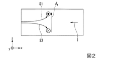
反強磁性体におけるスピンホール効果のメカニズムについてはまだ十分に理解されているとは言えず、従来の非磁性体におけるスピンホール効果のメカニズムと同じであるのか、異なるところがあるのか、現段階では確かではないが、図2を用いて、一般的に理解されているスピンホール効果により純スピン流が生み出されるメカニズムを説明する。 The mechanism of the spin Hall effect in antiferromagnets is not yet fully understood, and it is certain at this stage whether it is the same or different from the mechanism of the spin Hall effect in conventional nonmagnetic materials. However, the mechanism by which a pure spin current is generated by a generally understood spin Hall effect will be described with reference to FIG.
図2に示すように、スピン軌道トルク配線の延在方向に電流Iを流すと、紙面手前側に配向した第1スピンS1と紙面奥側に配向した第2スピンS2はそれぞれ電流と直交する方向に曲げられる。通常のホール効果とスピンホール効果とは運動(移動)する電荷(電子)が運動(移動)方向を曲げられる点で共通するが、通常のホール効果は磁場中で運動する荷電粒子がローレンツ力を受けて運動方向を曲げられるのに対して、スピンホール効果では磁場が存在しないのに電子が移動するだけ(電流が流れるだけ)で移動方向が曲げられる点で大きく異なる。 As shown in FIG. 2, when current I is passed in the extending direction of the spin orbit torque wiring, the first spin S1 oriented on the front side of the paper and the second spin S2 oriented on the back side of the paper are in directions orthogonal to the current, respectively. To be bent. The normal Hall effect and the spin Hall effect are common in that the moving (moving) charge (electrons) can bend in the moving (moving) direction, but the normal Hall effect is the charged particle moving in the magnetic field. In contrast to this, the direction of motion is bent, but the spin Hall effect is greatly different in that the direction of movement is bent only by the movement of electrons (only the current flows) even though no magnetic field exists.
非磁性体(強磁性体ではない材料)では第1スピンS1の電子数と第2スピンS2の電子数とが等しいので、図中で上方向に向かう第1スピンS1の電子数と下方向に向かう第2スピンS2の電子数が等しい。そのため、電荷の正味の流れとしての電流はゼロである。この電流を伴わないスピン流は特に純スピン流と呼ばれる。 Since the number of electrons of the first spin S1 and the number of electrons of the second spin S2 are equal in a non-magnetic material (a material that is not a ferromagnetic material), the number of electrons in the first spin S1 going upward in the figure and the downward direction The number of electrons of the second spin S2 heading is equal. Therefore, the current as a net flow of charge is zero. This spin current without current is particularly called a pure spin current.
強磁性体中に電流を流した場合は、第1スピンS1と第2スピンS2が互いに反対方向に曲げられる点は同じである。一方で、強磁性体中では第1スピンS1と第2スピンS2のいずれかが多い状態であり、結果として電荷の正味の流れが生じてしまう(電圧が発生してしまう)点が異なる。 When a current is passed through the ferromagnetic material, the first spin S1 and the second spin S2 are bent in the opposite directions. On the other hand, there is a large number of the first spin S1 and the second spin S2 in the ferromagnet, and as a result, a net flow of charges is generated (voltage is generated).
ここで、第1スピンS1のスピンの流れをJ↑、第2スピンS2のスピンの流れをJ↓、スピン流をJSと表すと、JS=J↑−J↓で定義される。図2においては、純スピン流としてJSが図中の上方向に流れる。ここで、JSは分極率が100%のスピンの流れである。 Here, if the spin flow of the first spin S1 is J ↑ , the spin flow of the second spin S2 is J ↓ , and the spin current is JS , JS = J ↑ −J ↓ . In FIG. 2, JS flows upward in the figure as a pure spin current. Here, J S is a spin flow with a polarizability of 100%.
図1において、反強磁性スピン軌道トルク配線5の上面に強磁性体を接触させると、純スピン流は強磁性体中に拡散して流れ込む。
In FIG. 1, when a ferromagnetic material is brought into contact with the upper surface of the antiferromagnetic spin
<磁化自由層>
磁化自由層10は、第1強磁性金属層1と第2強磁性金属層2と第1強磁性金属層1及び第2強磁性金属層2に挟持された第1非磁性層3とによって構成されるシンセティック構造を有する。磁化自由層10は、第1強磁性金属層1と第2強磁性金属層2と第1強磁性金属層1及び第2強磁性金属層2に挟持された第1非磁性層3とによって構成され、第1強磁性金属層1及び第2強磁性金属層2の磁化の向きが互いに反平行となるように可変とされている。
<Magnetic free layer>
The magnetization
第1強磁性金属層1及び第2強磁性金属層2は、磁化方向が層に平行な面内方向である面内磁化膜でも、磁化方向が層に対して垂直方向である垂直磁化膜でもいずれでもよい。
The first
第1強磁性金属層1及び第2強磁性金属層2の材料として、強磁性材料、特に軟磁性材料を適用できる。例えば、Cr、Mn、Co、Fe及びNiからなる群から選択される金属、これらの金属を1種以上含む合金、これらの金属とB、C、及びNの少なくとも1種以上の元素とが含まれる合金等を用いることができる。具体的には、Co−Fe、Co−Fe−B、Ni−Feが挙げられる。また、2層の強磁性金属層が非磁性層を介して生じる反強磁性結合(RKKY結合)は、2層の強磁性金属層と非磁性層のスピン軌道相互作用で働くことが知られており、Co/Ru/Coの構造の時にRKKY結合が強くなることが知られている。
第1強磁性金属層1及び第2強磁性金属層2の材料は同じであっても異なっていてもよい。
As the material of the first
The materials of the first
第1強磁性金属層1及び第2強磁性金属層2は、飽和磁化と体積の積が等しくなるように構成されていることが好ましい。
本実施形態のスピン流磁化反転素子においては、第1強磁性金属層1及び第2強磁性金属層2の飽和磁化と体積の積が等しくなることで、RKKY結合が強くなる。強いRKKY結合により、読み出し時に反強磁性スピン軌道トルク配線に流れる電流が生み出す電流磁界に対して、 第1強磁性金属層1が揺らぎにくくなる。
The first
In the spin current magnetization switching element of the present embodiment, the RKKY coupling is strengthened by equalizing the product of the saturation magnetization and volume of the first
第1非磁性層3としては、第1強磁性金属層1と第2強磁性金属層2との間の反強磁性結合(RKKY結合)を介在できる非磁性金属材料であれば特に制限はないが、例えば、Cr、Cu、Mo、Ru、Rh、Re及びIrのからなる群から選択された非磁性金属からなるものを用いることができる。
The first
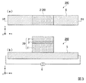
図3に、本発明の他の実施形態に係るスピン流磁化反転素子の一例の模式図を示す。図3(a)は平面図であり、図3(b)は図3(a)の反強磁性スピン軌道トルク配線5の幅方向の中心線であるX−X線で切った断面図である。図1と同様な構成について、同じ符号を用いて説明を省略する。
図3に示すスピン流磁化反転素子200においては、磁化自由層20を構成する第1強磁性金属層11及び2強磁性金属層2のうち、第1強磁性金属層11の膜厚が第2強磁性金属層2の膜厚より厚い点が図1に示すスピン流磁化反転素子100と異なる。
本実施形態のスピン流磁化反転素子においては、第1強磁性金属層の膜厚を厚くすることによって、第2強磁性金属層への純スピンの拡散を低減することができる上、第1強磁性金属層のバルク散乱効果を用いることでMR比を向上することができる。
FIG. 3 shows a schematic diagram of an example of a spin current magnetization switching element according to another embodiment of the present invention. 3A is a plan view, and FIG. 3B is a cross-sectional view taken along the line XX, which is the center line in the width direction of the antiferromagnetic spin
In the spin current
In the spin current magnetization switching element of this embodiment, by increasing the film thickness of the first ferromagnetic metal layer, it is possible to reduce the diffusion of pure spins into the second ferromagnetic metal layer and The MR ratio can be improved by using the bulk scattering effect of the magnetic metal layer.
限定するわけではないが、本実施形態の上記効果を奏するための膜厚の目安を例示すれば、第1強磁性金属層11の膜厚を1.0〜10.0nm、第2強磁性金属層2の膜厚を0.5〜5.0nmとし、膜厚の差としては例えば、0.5〜9.5nmとすることができる。
The film thickness of the first
図4に、本発明の他の実施形態に係るスピン流磁化反転素子の一例の模式図を示す。図4(a)は平面図であり、図4(b)は図4(a)の反強磁性スピン軌道トルク配線5の幅方向の中心線であるX−X線で切った断面図である。図1と同様な構成について、同じ符号を用いて説明を省略する。
図4に示すスピン流磁化反転素子300においては、磁化自由層30を構成する第1強磁性金属層21及び2強磁性金属層2のうち、第1強磁性金属層21の膜厚が第2強磁性金属層2の膜厚より薄く、第1強磁性金属層21の面直方向から平面視したときの面積が、第2強磁性金属層2の面直方向から平面視したときの面積より大きい点が図1に示すスピン流磁化反転素子100と異なる。
本実施形態のスピン流磁化反転素子においては、第1強磁性金属層の膜厚を薄くすることで反転電流を小さくすることができる。膜厚を薄くすると熱安定性が低下するが、上述の通り、RKKY結合することで熱安定性を確保できる。
また、第1強磁性金属層21の膜厚が薄い分、面積を大きくすることで体積の低減を抑え、それによって、RKKY結合の大きさの低下を低減できる。
FIG. 4 shows a schematic diagram of an example of a spin current magnetization switching element according to another embodiment of the present invention. 4A is a plan view, and FIG. 4B is a cross-sectional view taken along the line XX which is the center line in the width direction of the antiferromagnetic spin
In the spin current
In the spin current magnetization switching element of this embodiment, the switching current can be reduced by reducing the thickness of the first ferromagnetic metal layer. When the film thickness is reduced, the thermal stability is lowered. However, as described above, thermal stability can be ensured by RKKY bonding.
In addition, since the first
限定するわけではないが、本実施形態の上記効果を奏するための膜厚の目安を例示すれば、第1強磁性金属層21の膜厚を0.5〜5.0nm、第2強磁性金属層2の膜厚を1.0〜10.0nmとし、膜厚の差としては例えば、0.5〜9.5nmとすることができる。
The film thickness of the first
本発明のスピン流磁化反転素子は後述するように磁気抵抗効果素子に適用することができる。用途としては磁気抵抗効果素子に限られず、他の用途にも適用できる。他の用途としては、例えば、上記のスピン流磁化反転素子を各画素に配設して、磁気光学効果を利用して入射光を空間的に変調する空間光変調器においても用いることができるし、磁気センサにおいて磁石の保磁力によるヒステリシスの効果を避けるために磁石の磁化容易軸に印加する磁場を反強磁性スピン軌道トルク配線(スピン流磁化反転素子)に置き換えてもよい。 The spin current magnetization reversal element of the present invention can be applied to a magnetoresistive effect element as will be described later. The use is not limited to the magnetoresistive effect element, and can be applied to other uses. Other applications include, for example, a spatial light modulator that spatially modulates incident light using the magneto-optic effect by disposing the above-described spin current magnetization reversal element in each pixel. In order to avoid the effect of hysteresis due to the coercive force of the magnet in the magnetic sensor, the magnetic field applied to the easy magnetization axis of the magnet may be replaced with an antiferromagnetic spin orbit torque wiring (spin current magnetization reversal element).
(磁気抵抗効果素子)
本発明の一実施形態に係る磁気抵抗効果素子は、本発明のスピン流磁化反転素子と、磁化の向きが固定された磁化固定層と、第2強磁性金属層と磁化固定層に挟持された第2非磁性層とを備えるものである。
(Magnetoresistive element)
A magnetoresistive effect element according to an embodiment of the present invention is sandwiched between a spin current magnetization reversal element of the present invention, a magnetization fixed layer whose magnetization direction is fixed, a second ferromagnetic metal layer, and a magnetization fixed layer. And a second nonmagnetic layer.
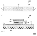
図5は、本発明のスピン流磁化反転素子の応用例であり、また、本発明の一実施形態に係る磁気抵抗効果素子でもある磁気抵抗効果素子の一例の模式図を示す。図5(a)は平面図であり、図5(b)は図5(a)の反強磁性スピン軌道トルク配線120の幅方向の中心線であるX−X線で切った断面図である。
図5に示す磁気抵抗効果素子1000は、本発明のスピン流磁化反転素子(磁化自由層101と反強磁性スピン軌道トルク配線120)と、磁化の向きが固定された磁化固定層103と、磁化自由層101及び磁化固定層103に挟持された第2非磁性層102とを有する。また、図3に示す磁気抵抗効果素子1000は、磁気抵抗効果素子部105と反強磁性スピン軌道トルク配線120とを有するということもできる。
図5においては、磁気抵抗効果素子1000を作製する基板110と、キャップ層104及び配線130も図示した。
FIG. 5 is a schematic diagram of an example of a magnetoresistive effect element that is an application example of the spin current magnetization reversal element of the present invention and is also a magnetoresistive effect element according to an embodiment of the present invention. 5A is a plan view, and FIG. 5B is a cross-sectional view taken along the line XX, which is the center line in the width direction of the antiferromagnetic spin
A
In FIG. 5, the
本発明の一実施形態に係る磁気抵抗効果素子1000は、反強磁性スピン軌道トルク配線120を備えることで、純スピン流によるSOTのみで磁気抵抗効果素子の磁化反転を行う構成(以下、「SOTのみ」構成ということがある)とすることもできるし、従来のSTTを利用する磁気抵抗効果素子において純スピン流によるSOTを併用する構成(以下、「STT及びSOT併用」構成ということがある)とすることもできる。STTを利用する場合には、磁気抵抗効果素子1000の積層方向に電流を流すための配線130が必要となり、配線は磁化固定層103上に直接、または、他の層例えば、キャップ層104を介して形成される。
A
以下では、スピン軌道トルク配線が磁気抵抗効果素子部の積層方向に対して交差する方向に延在する構成の例として、直交する方向に延在する構成の場合について説明する。 Hereinafter, as an example of a configuration in which the spin orbit torque wiring extends in a direction intersecting the stacking direction of the magnetoresistive effect element portion, a case of a configuration extending in an orthogonal direction will be described.
<磁気抵抗効果素子部>
磁気抵抗効果素子部105は、磁化の向きが固定された磁化固定層103と、磁化の向きが可変な磁化自由層101と、磁化固定層103及び磁化自由層101に挟持された第2非磁性層102とを有する。
磁化固定層103の磁化が一方向に固定され、磁化自由層101の磁化の向きが相対的に変化することで、磁気抵抗効果素子部105として機能する。保磁力差型(擬似スピンバルブ型;Pseudo spin valve 型)のMRAMに適用する場合には、第2強磁性金属層の保持力は第1強磁性金属層の保磁力よりも大きいものであり、また、交換バイアス型(スピンバルブ;spin valve型)のMRAMに適用する場合には、第2強磁性金属層では反強磁性層との交換結合によって磁化の向きが固定される。
また、磁気抵抗効果素子部105は、第2非磁性層102が絶縁体からなる場合は、トンネル磁気抵抗(TMR:Tunneling Magnetoresistance)素子であり、第2非磁性層102が金属からなる場合は巨大磁気抵抗(GMR:Giant Magnetoresistance)素子である。
<Magnetoresistance effect element>
The magnetoresistive
The magnetization of the magnetization fixed
Further, the magnetoresistive
本発明が備える磁気抵抗効果素子部としては、公知の磁気抵抗効果素子部の構成を用いることができる。例えば、各層は複数の層からなるものでもよいし、第2強磁性金属層の磁化の向きを固定するための反強磁性層等の他の層を備えてもよい。
磁化固定層103は磁化固定層や参照層、磁化自由層101は磁化自由層や記憶層などと呼ばれる。
As a magnetoresistive effect element portion provided in the present invention, a configuration of a known magnetoresistive effect element portion can be used. For example, each layer may be composed of a plurality of layers, or may be provided with other layers such as an antiferromagnetic layer for fixing the magnetization direction of the second ferromagnetic metal layer.
The magnetization fixed
磁化固定層103は、磁化方向が層に平行な面内方向である面内磁化膜でも、磁化方向が層に対して垂直方向である垂直磁化膜でもいずれでもよい。
The magnetization fixed
第3強磁性金属層である磁化固定層103の材料には、公知のものを用いることができる。例えば、Cr、Mn、Co、Fe及びNiからなる群から選択される金属及びこれらの金属を1種以上含み強磁性を示す合金を用いることができる。またこれらの金属と、B、C、及びNの少なくとも1種以上の元素とを含む合金を用いることもできる。具体的には、Co−FeやCo−Fe−Bが挙げられる。
A known material can be used as the material of the magnetization fixed
また、より高い出力を得るためにはCo2FeSiなどのホイスラー合金を用いることが好ましい。ホイスラー合金は、X2YZの化学組成をもつ金属間化合物を含み、Xは、周期表上でCo、Fe、Ni、あるいはCu族の遷移金属元素または貴金属元素であり、Yは、Mn、V、CrあるいはTi族の遷移金属でありXの元素種をとることもでき、Zは、III族からV族の典型元素である。例えば、Co2FeSi、Co2MnSiやCo2Mn1−aFeaAlbSi1−bなどが挙げられる。 In order to obtain a higher output, it is preferable to use a Heusler alloy such as Co 2 FeSi. The Heusler alloy includes an intermetallic compound having a chemical composition of X 2 YZ, where X is a transition metal element or noble metal element of Co, Fe, Ni, or Cu group on the periodic table, and Y is Mn, V It is a transition metal of Cr, Ti or Ti, and can take the elemental species of X, and Z is a typical element of Group III to Group V. Examples thereof include Co 2 FeSi, Co 2 MnSi, and Co 2 Mn 1-a Fe a Al b Si 1-b .
また、磁化固定層103の磁化自由層101に対する保磁力をより大きくするために、磁化固定層103と接する材料としてIrMn、PtMnなどの反強磁性材料を用いてもよい。
Further, in order to increase the coercive force of the magnetization fixed
さらに、磁化固定層103の漏れ磁場を磁化自由層101に影響させないようにするため、磁化固定層103はシンセティック構造を有するものとしてもよい。
磁化固定層103もシンセティック構造であることによって、さらに熱安定性を確保することができる。
Furthermore, in order not to affect the leakage magnetic field of the magnetization fixed
Since the magnetization fixed
さらに磁化固定層103の磁化の向きを積層面に対して垂直にする場合には、CoとPtの積層膜を用いることが好ましい。具体的には、磁化固定層103は[Co(0.24nm)/Pt(0.16nm)]6/Ru(0.9nm)/[Pt(0.16nm)/Co(0.16nm)]4/Ta(0.2nm)/FeB(1.0nm)とすることができる。
Further, when the magnetization direction of the magnetization fixed
第2非磁性層102には、公知の材料を用いることができる。
例えば、第2非磁性層102が絶縁体からなる場合(トンネルバリア層である場合)、その材料としては、Al2O3、SiO2、MgO、及び、MgAl2O4等を用いることができる。またこれらの他にも、Al、Si、Mgの一部が、Zn、Be等に置換された材料等も用いることができる。これらの中でも、MgOやMgAl2O4はコヒーレントトンネルが実現できる材料であるため、スピンを効率よく注入できる。
また、第2非磁性層102が金属からなる場合、その材料としては、Cu、Au、Ag等を用いることができる。
A known material can be used for the second
For example, when the second
When the second
また、磁化固定層103の第2非磁性層102と反対側の面には、キャップ層104を備えることが好ましい。キャップ層104は、磁化固定層103からの元素の拡散を抑制することができる。またキャップ層104は、磁気抵抗効果素子部105の各層の結晶配向性にも寄与する。その結果、キャップ層104を設けることで、磁気抵抗効果素子部105の磁化固定層103及び磁化自由層101の磁性を安定化し、磁気抵抗効果素子部105を低抵抗化することができる。
Further, it is preferable to provide a
キャップ層104には、導電性が高い材料を用いることが好ましい。例えば、Ru、Ta、Cu、Ag、Au等を用いることができる。キャップ層104の結晶構造は、隣接する強磁性金属層の結晶構造に合せて、fcc構造、hcp構造またはbcc構造から適宜設定することが好ましい。
It is preferable to use a material having high conductivity for the
また、キャップ層104には、銀、銅、マグネシウム、及び、アルミニウムからなる群から選択されるいずれかを用いることが好ましい。
In addition, it is preferable to use any one selected from the group consisting of silver, copper, magnesium, and aluminum for the
<基板>
基板110は、平坦性に優れることが好ましい。平坦性に優れた表面を得るために、材料として例えば、Si、AlTiC等を用いることができる。
<Board>
The
基板110の反強磁性スピン軌道トルク配線120側の面には、下地層(図示略)が形成されていてもよい。下地層を設けると、基板110上に積層される反強磁性スピン軌道トルク配線120を含む各層の結晶配向性、結晶粒径等の結晶性を制御することができる。
An underlayer (not shown) may be formed on the surface of the
下地層は、絶縁性を有していることが好ましい。反強磁性スピン軌道トルク配線120等に流れる電流が散逸しないようにするためである。下地層には、種々のものを用いることができる。
例えば1つの例として、下地層には(001)配向したNaCl構造を有し、Ti、Zr、Nb、V、Hf、Ta、Mo、W、B、Al、Ceの群から選択される少なくとも1つの元素を含む窒化物の層を用いることができる。
The underlayer preferably has an insulating property. This is to prevent the current flowing in the antiferromagnetic spin
For example, as one example, the underlayer has a (001) -oriented NaCl structure and is at least one selected from the group consisting of Ti, Zr, Nb, V, Hf, Ta, Mo, W, B, Al, and Ce. A nitride layer containing two elements can be used.
他の例として、下地層にはXYO3の組成式で表される(002)配向したペロブスカイト系導電性酸化物の層を用いることができる。ここで、サイトXはSr、Ce、Dy、La、K、Ca、Na、Pb、Baの群から選択された少なくとも1つの元素を含み、サイトYはTi、V、Cr、Mn、Fe、Co、Ni、Ga、Nb、Mo、Ru、Ir、Ta、Ce、Pbの群から選択された少なくとも1つの元素を含む。 As another example, a (002) -oriented perovskite conductive oxide layer represented by a composition formula of XYO 3 can be used for the underlayer. Here, the site X includes at least one element selected from the group of Sr, Ce, Dy, La, K, Ca, Na, Pb, and Ba, and the site Y includes Ti, V, Cr, Mn, Fe, and Co. , Ni, Ga, Nb, Mo, Ru, Ir, Ta, Ce, and Pb.
他の例として、下地層には(001)配向したNaCl構造を有し、かつMg、Al、Ceの群から選択される少なくとも1つの元素を含む酸化物の層を用いることができる。 As another example, an oxide layer having a (001) -oriented NaCl structure and containing at least one element selected from the group consisting of Mg, Al, and Ce can be used for the base layer.
他の例として、下地層には(001)配向した正方晶構造または立方晶構造を有し、かつAl、Cr、Fe、Co、Rh、Pd、Ag、Ir、Pt、Au、Mo、Wの群から選択される少なくとも1つの元素を含む層を用いることができる。 As another example, the base layer has a (001) -oriented tetragonal structure or cubic structure, and Al, Cr, Fe, Co, Rh, Pd, Ag, Ir, Pt, Au, Mo, W A layer containing at least one element selected from the group can be used.
また、下地層は一層に限られず、上述の例の層を複数層積層してもよい。下地層の構成を工夫することにより磁気抵抗効果素子部105の各層の結晶性を高め、磁気特性の改善が可能となる。
Further, the underlayer is not limited to a single layer, and a plurality of layers in the above example may be stacked. By devising the configuration of the underlayer, the crystallinity of each layer of the
<配線>
配線130は、磁気抵抗効果素子部105の磁化固定層103に電気的に接続され、図5においては、配線130と反強磁性スピン軌道トルク配線120と電源(図示略)とで閉回路を構成し、磁気抵抗効果素子部105の積層方向に電流が流される。
<Wiring>
The
配線130は、導電性の高い材料であれば特に問わない。例えば、アルミニウム、銀、銅、金等を用いることができる。
The
図5に示した磁気抵抗効果素子1000において、基板110から遠い側に磁化固定層(ピン層)が配置するいわゆるボトムピン構造の例を挙げたが、磁気抵抗効果素子1000の構造は特に限定されるものではなく、いわゆるトップピン構造であってもよい。
In the
(磁気メモリ)
本発明の磁気メモリ(MRAM)は、本発明の磁気抵抗効果素子を複数備える。
(Magnetic memory)
The magnetic memory (MRAM) of the present invention includes a plurality of magnetoresistive elements of the present invention.
(製造方法)
本発明のスピン流磁化反転素子は、スパッタリング法等の公知の成膜技術と、フォトリソグラフィー及びArイオンミリング等の公知の形状加工技術を用いて得ることができる。以下では、スピン流磁化反転素子を適用した磁気抵抗効果素子の製造方法について説明することでスピン流磁化反転素子の製造方法の説明も兼ねる。
(Production method)
The spin current magnetization reversal element of the present invention can be obtained by using a known film forming technique such as sputtering and a known shape processing technique such as photolithography and Ar ion milling. In the following, a method for manufacturing a magneto-resistance effect element to which a spin current magnetization reversal element is applied will be described to also explain a method for manufacturing a spin current magnetization reversal element.
まず支持体となる基板上に反強磁性スピン軌道トルク配線を作製する。反強磁性スピン軌道トルク配線を構成する金属の層をスパッタ法を用いて成膜する。反強磁性スピン軌道トルク配線を構成するが合金である場合には、2元同時スパッタ法を用いて成膜する。組成比の調整は、印加DC電圧を変え各々のスパッタリングレートを調整することで種々の組成比を実現することができる。次いで、フォトリソグラフィー等の技術を用いて、反強磁性スピン軌道トルク配線を所定の形状に加工する。 First, an antiferromagnetic spin orbit torque wiring is fabricated on a substrate serving as a support. A metal layer constituting the antiferromagnetic spin orbit torque wiring is formed by sputtering. When the antiferromagnetic spin orbit torque wiring is constituted but is an alloy, the film is formed by using the binary simultaneous sputtering method. The composition ratio can be adjusted by changing the applied DC voltage and adjusting each sputtering rate to realize various composition ratios. Next, the antiferromagnetic spin orbit torque wiring is processed into a predetermined shape using a technique such as photolithography.
そして、反強磁性スピン軌道トルク配線以外の部分は、酸化膜等の絶縁膜で覆う。反強磁性スピン軌道トルク配線及び絶縁膜の露出面は、化学機械研磨(CMP)により研磨することが好ましい。 The portions other than the antiferromagnetic spin orbit torque wiring are covered with an insulating film such as an oxide film. The antiferromagnetic spin orbit torque wiring and the exposed surface of the insulating film are preferably polished by chemical mechanical polishing (CMP).
次いで、磁気抵抗効果素子を作製する。磁気抵抗効果素子はスパッタリング等の公知の成膜手段を用いて作製できる。磁気抵抗効果素子がTMR素子の場合、例えば、トンネルバリア層は第1強磁性金属層上に最初に0.4〜2.0nm程度のマグネシウム、アルミニウム、及び複数の非磁性元素の二価の陽イオンとなる金属薄膜をスパッタリングし、プラズマ酸化あるいは酸素導入による自然酸化を行い、その後の熱処理によって形成される。成膜法としてはスパッタリング法のほか、蒸着法、レーザアブレーション法、MBE法等が挙げられる。 Next, a magnetoresistive effect element is manufactured. The magnetoresistive element can be manufactured using a known film forming means such as sputtering. When the magnetoresistive element is a TMR element, for example, the tunnel barrier layer is initially formed of a divalent positive electrode of magnesium, aluminum, and a plurality of nonmagnetic elements of about 0.4 to 2.0 nm on the first ferromagnetic metal layer. It is formed by sputtering a metal thin film that becomes ions, performing natural oxidation by plasma oxidation or oxygen introduction, and subsequent heat treatment. Examples of the film forming method include sputtering, vapor deposition, laser ablation, and MBE.
得られた積層膜は、アニール処理することが好ましい。反応性スパッタで形成した層は、アモルファスであり結晶化する必要がある。例えば、強磁性金属層としてCo−Fe−Bを用いる場合は、Bの一部がアニール処理により抜けて結晶化する。 The obtained laminated film is preferably annealed. The layer formed by reactive sputtering is amorphous and needs to be crystallized. For example, when Co—Fe—B is used as the ferromagnetic metal layer, a part of B is removed by the annealing process and crystallizes.
アニール処理して製造した磁気抵抗効果素子は、アニール処理しないで製造した磁気抵抗効果素子と比較して、MR比が向上する。アニール処理によって、非磁性層3のトンネルバリア層の結晶サイズの均一性および配向性が向上するためであると考えられる。
A magnetoresistive effect element manufactured by annealing treatment has an improved MR ratio compared to a magnetoresistive effect element manufactured without annealing treatment. This is probably because the annealing process improves the uniformity and orientation of the crystal size of the tunnel barrier layer of the
アニール処理としては、Arなどの不活性雰囲気中で、300℃以上500℃以下の温度で、5分以上100分以下の時間加熱した後、2kOe以上10kOe以下の磁場を印加した状態で、100℃以上500℃以下の温度で、1時間以上10時間以下の時間加熱することが好ましい。 As the annealing treatment, heating is performed at a temperature of 300 ° C. or higher and 500 ° C. or lower for 5 minutes to 100 minutes in an inert atmosphere such as Ar, and then a magnetic field of 2 kOe or higher and 10 kOe or lower is applied. It is preferable to heat at a temperature of 500 ° C. or lower for 1 hour to 10 hours.
磁気抵抗効果素子を所定の形状にする方法としては、フォトリソグラフィー等の公知の加工手段を利用できる。まず磁気抵抗効果素子を積層した後、磁気抵抗効果素子の反強磁性スピン軌道トルク配線と反対側の面に、レジストを塗工する。そして、所定の部分のレジストを硬化し、不要部のレジストを除去する。レジストが硬化した部分は、磁気抵抗効果素子の保護膜となる。レジストが硬化した部分は、最終的に得られる磁気抵抗効果素子の形状と一致する。 As a method for making the magnetoresistive element into a predetermined shape, known processing means such as photolithography can be used. First, after the magnetoresistive effect element is stacked, a resist is applied to the surface of the magnetoresistive effect element opposite to the antiferromagnetic spin orbit torque wiring. Then, a predetermined portion of the resist is cured, and unnecessary portions of the resist are removed. The portion where the resist is cured serves as a protective film for the magnetoresistive element. The portion where the resist is cured matches the shape of the finally obtained magnetoresistive element.
そして、保護膜が形成された面に、イオンミリング、反応性イオンエッチング(RIE)等の処理を施す。保護膜が形成されていない部分は除去され、所定の形状の磁気抵抗効果素子が得られる。 Then, treatment such as ion milling and reactive ion etching (RIE) is performed on the surface on which the protective film is formed. The portion where the protective film is not formed is removed, and a magnetoresistive element having a predetermined shape is obtained.
1 第1強磁性金属層
2 第2強磁性金属層
3 第1非磁性層
5 反強磁性スピン軌道トルク配線
10 磁化自由層
100、200、300 スピン流磁化反転素子
101 磁化自由層
102第2非磁性層
103 磁化固定層
105 磁気抵抗効果素子部
1000 磁気抵抗効果素子
DESCRIPTION OF
Claims (10)
前記シンセティック構造の積層方向である第1方向に対して交差する第2方向に延在し、前記第1強磁性金属層に接合する反強磁性スピン軌道トルク配線と、を備え、
前記反強磁性スピン軌道トルク配線に通電することによって、前記磁化自由層の磁化の向きを変化させるスピン流磁化反転素子。 A magnetization free layer having a synthetic structure composed of a first ferromagnetic metal layer, a second ferromagnetic metal layer, the first ferromagnetic metal layer, and a first nonmagnetic layer sandwiched between the second ferromagnetic metal layer When,
An antiferromagnetic spin orbit torque wiring extending in a second direction intersecting with the first direction which is a stacking direction of the synthetic structure and joining to the first ferromagnetic metal layer,
A spin current magnetization reversal element that changes the magnetization direction of the magnetization free layer by energizing the antiferromagnetic spin orbit torque wiring.
磁化の向きが固定された磁化固定層と、
前記第2強磁性金属層と前記磁化固定層とに挟持された第2非磁性層とを備える磁気抵抗効果素子。 The spin current magnetization reversal element according to any one of claims 1 to 6,
A magnetization fixed layer in which the direction of magnetization is fixed;
A magnetoresistive effect element comprising: a second nonmagnetic layer sandwiched between the second ferromagnetic metal layer and the magnetization fixed layer.
前記磁化自由層の積層方向である第1方向に対して交差する第2方向に延在し、前記第1強磁性金属層に接合する反強磁性スピン軌道トルク配線と、を備え、
前記反強磁性スピン軌道トルク配線に通電することによって、前記磁化自由層の磁化の向きを変化させるスピン流磁化反転素子。 The first ferromagnetic metal layer includes a first ferromagnetic metal layer, a second ferromagnetic metal layer, the first ferromagnetic metal layer, and a first nonmagnetic layer sandwiched between the second ferromagnetic metal layer. A magnetization free layer that is variable so that the magnetization directions of the second ferromagnetic metal layers are antiparallel to each other;
An antiferromagnetic spin orbit torque wiring extending in a second direction intersecting the first direction which is the stacking direction of the magnetization free layer and joining to the first ferromagnetic metal layer,
A spin current magnetization reversal element that changes the magnetization direction of the magnetization free layer by energizing the antiferromagnetic spin orbit torque wiring.
Priority Applications (2)
| Application Number | Priority Date | Filing Date | Title |
|---|---|---|---|
| JP2016235236A JP6972542B2 (en) | 2016-12-02 | 2016-12-02 | Spin current magnetization reversal element, magnetoresistive element and magnetic memory |
| US15/827,852 US10276785B2 (en) | 2016-12-02 | 2017-11-30 | Spin current magnetization rotational element, magnetoresistance effect element, and magnetic memory |
Applications Claiming Priority (1)
| Application Number | Priority Date | Filing Date | Title |
|---|---|---|---|
| JP2016235236A JP6972542B2 (en) | 2016-12-02 | 2016-12-02 | Spin current magnetization reversal element, magnetoresistive element and magnetic memory |
Publications (2)
| Publication Number | Publication Date |
|---|---|
| JP2018093059A true JP2018093059A (en) | 2018-06-14 |
| JP6972542B2 JP6972542B2 (en) | 2021-11-24 |
Family
ID=62243893
Family Applications (1)
| Application Number | Title | Priority Date | Filing Date |
|---|---|---|---|
| JP2016235236A Active JP6972542B2 (en) | 2016-12-02 | 2016-12-02 | Spin current magnetization reversal element, magnetoresistive element and magnetic memory |
Country Status (2)
| Country | Link |
|---|---|
| US (1) | US10276785B2 (en) |
| JP (1) | JP6972542B2 (en) |
Cited By (2)
| Publication number | Priority date | Publication date | Assignee | Title |
|---|---|---|---|---|
| WO2020110296A1 (en) * | 2018-11-30 | 2020-06-04 | Tdk株式会社 | Spin-orbit torque magnetization rotation element, spin-orbit torque magnetoresistance effect element, magnetic memory, and high-frequency magnetic element |
| JP2020150142A (en) * | 2019-03-14 | 2020-09-17 | 株式会社東芝 | Magnetic storage device |
Families Citing this family (8)
| Publication number | Priority date | Publication date | Assignee | Title |
|---|---|---|---|---|
| JP7024204B2 (en) * | 2017-04-21 | 2022-02-24 | Tdk株式会社 | Spin current magnetization rotating element, magnetoresistive element and magnetic memory |
| WO2019049591A1 (en) | 2017-09-07 | 2019-03-14 | Tdk株式会社 | Spin current magnetization reversal element and spin orbit torque type magnetic resistance effect element |
| US11393515B2 (en) * | 2018-06-14 | 2022-07-19 | Intel Corporation | Transition metal dichalcogenide based spin orbit torque memory device |
| TWI678820B (en) * | 2018-08-02 | 2019-12-01 | 世界先進積體電路股份有限公司 | Magnetoresistive devices and methods for forming the same |
| KR102517332B1 (en) | 2018-09-12 | 2023-04-03 | 삼성전자주식회사 | Semiconductor device including spin-orbit torque line and method of operating the same |
| EP3731289A1 (en) | 2019-04-23 | 2020-10-28 | IMEC vzw | A magnetic tunnel junction device |
| CN111986717A (en) * | 2020-08-20 | 2020-11-24 | 中国科学院微电子研究所 | SOT-MRAM (spin on demand-random Access memory) without external magnetic field oriented spin reversal and array |
| CN113437211A (en) * | 2021-06-25 | 2021-09-24 | 上海理工大学 | Terahertz wave modulator based on magnetic tunnel junction and preparation method thereof |
Citations (5)
| Publication number | Priority date | Publication date | Assignee | Title |
|---|---|---|---|---|
| JP2005174969A (en) * | 2003-12-05 | 2005-06-30 | Japan Science & Technology Agency | Magnetic random-access memory cell using magnetostatic coupling |
| JP2014045196A (en) * | 2012-08-26 | 2014-03-13 | Samsung Electronics Co Ltd | Magnetic tunneling junction using spin-orbit interaction based on switching, and method and system for providing memory utilizing magnetic tunneling junction |
| WO2016159017A1 (en) * | 2015-03-31 | 2016-10-06 | 国立大学法人東北大学 | Magnetic resistance effect element, magnetic memory device, manufacturing method, operation method, and integrated circuit |
| US20160300999A1 (en) * | 2015-04-07 | 2016-10-13 | Ge Yi | Magnetoresistive Random Access Memory Cell |
| WO2016182354A1 (en) * | 2015-05-13 | 2016-11-17 | 고려대학교 산학협력단 | Magnetic memory device |
Family Cites Families (2)
| Publication number | Priority date | Publication date | Assignee | Title |
|---|---|---|---|---|
| FR2963153B1 (en) | 2010-07-26 | 2013-04-26 | Centre Nat Rech Scient | INDEXABLE MAGNETIC ELEMENT |
| US9105830B2 (en) * | 2012-08-26 | 2015-08-11 | Samsung Electronics Co., Ltd. | Method and system for providing dual magnetic tunneling junctions using spin-orbit interaction-based switching and memories utilizing the dual magnetic tunneling junctions |
-
2016
- 2016-12-02 JP JP2016235236A patent/JP6972542B2/en active Active
-
2017
- 2017-11-30 US US15/827,852 patent/US10276785B2/en active Active
Patent Citations (5)
| Publication number | Priority date | Publication date | Assignee | Title |
|---|---|---|---|---|
| JP2005174969A (en) * | 2003-12-05 | 2005-06-30 | Japan Science & Technology Agency | Magnetic random-access memory cell using magnetostatic coupling |
| JP2014045196A (en) * | 2012-08-26 | 2014-03-13 | Samsung Electronics Co Ltd | Magnetic tunneling junction using spin-orbit interaction based on switching, and method and system for providing memory utilizing magnetic tunneling junction |
| WO2016159017A1 (en) * | 2015-03-31 | 2016-10-06 | 国立大学法人東北大学 | Magnetic resistance effect element, magnetic memory device, manufacturing method, operation method, and integrated circuit |
| US20160300999A1 (en) * | 2015-04-07 | 2016-10-13 | Ge Yi | Magnetoresistive Random Access Memory Cell |
| WO2016182354A1 (en) * | 2015-05-13 | 2016-11-17 | 고려대학교 산학협력단 | Magnetic memory device |
Cited By (2)
| Publication number | Priority date | Publication date | Assignee | Title |
|---|---|---|---|---|
| WO2020110296A1 (en) * | 2018-11-30 | 2020-06-04 | Tdk株式会社 | Spin-orbit torque magnetization rotation element, spin-orbit torque magnetoresistance effect element, magnetic memory, and high-frequency magnetic element |
| JP2020150142A (en) * | 2019-03-14 | 2020-09-17 | 株式会社東芝 | Magnetic storage device |
Also Published As
| Publication number | Publication date |
|---|---|
| US10276785B2 (en) | 2019-04-30 |
| JP6972542B2 (en) | 2021-11-24 |
| US20180159026A1 (en) | 2018-06-07 |
Similar Documents
| Publication | Publication Date | Title |
|---|---|---|
| JP7168922B2 (en) | Spin current magnetization reversal device, magnetoresistive effect device and magnetic memory | |
| JP6607302B2 (en) | Spin current magnetization rotation element, magnetoresistive effect element, and magnetic memory | |
| JP6972542B2 (en) | Spin current magnetization reversal element, magnetoresistive element and magnetic memory | |
| JP6642680B2 (en) | Spin current magnetization rotating element, magnetoresistive element and magnetic memory | |
| JP6496098B2 (en) | Spin current magnetization reversal element, magnetoresistive effect element, and magnetic memory | |
| JP2019057626A (en) | Spin current magnetization reversal element, spin orbit torque type magnetoresistance effect element, and magnetic memory | |
| WO2019167198A1 (en) | Stabilization method for spin elements and production method for spin elements | |
| WO2018101028A1 (en) | Spin current magnetization reversal element, method of manufacturing same, magneto resistive sensor, and magnetic memory | |
| JP4061590B2 (en) | Magnetic thin film, magnetoresistive effect element and magnetic device using the same | |
| JP2005228998A (en) | Magnetic thin film and magnetoresistance effect element and magnetic device using it | |
| CN111512456B (en) | Ferromagnetic laminated film, spin-flow magnetization rotating element, magnetoresistance effect element, and magnetic memory |
Legal Events
| Date | Code | Title | Description |
|---|---|---|---|
| A621 | Written request for application examination |
Free format text: JAPANESE INTERMEDIATE CODE: A621 Effective date: 20190716 |
|
| A977 | Report on retrieval |
Free format text: JAPANESE INTERMEDIATE CODE: A971007 Effective date: 20200521 |
|
| A131 | Notification of reasons for refusal |
Free format text: JAPANESE INTERMEDIATE CODE: A131 Effective date: 20200602 |
|
| A601 | Written request for extension of time |
Free format text: JAPANESE INTERMEDIATE CODE: A601 Effective date: 20200803 |
|
| A521 | Request for written amendment filed |
Free format text: JAPANESE INTERMEDIATE CODE: A523 Effective date: 20201001 |
|
| A131 | Notification of reasons for refusal |
Free format text: JAPANESE INTERMEDIATE CODE: A131 Effective date: 20210406 |
|
| A521 | Request for written amendment filed |
Free format text: JAPANESE INTERMEDIATE CODE: A523 Effective date: 20210602 |
|
| TRDD | Decision of grant or rejection written | ||
| A01 | Written decision to grant a patent or to grant a registration (utility model) |
Free format text: JAPANESE INTERMEDIATE CODE: A01 Effective date: 20211005 |
|
| A61 | First payment of annual fees (during grant procedure) |
Free format text: JAPANESE INTERMEDIATE CODE: A61 Effective date: 20211018 |
|
| R150 | Certificate of patent or registration of utility model |
Ref document number: 6972542 Country of ref document: JP Free format text: JAPANESE INTERMEDIATE CODE: R150 |