JP2018091804A - Semiconductor device - Google Patents
Semiconductor device Download PDFInfo
- Publication number
- JP2018091804A JP2018091804A JP2016237421A JP2016237421A JP2018091804A JP 2018091804 A JP2018091804 A JP 2018091804A JP 2016237421 A JP2016237421 A JP 2016237421A JP 2016237421 A JP2016237421 A JP 2016237421A JP 2018091804 A JP2018091804 A JP 2018091804A
- Authority
- JP
- Japan
- Prior art keywords
- cumulative
- circuit
- count value
- stress
- value
- Prior art date
- Legal status (The legal status is an assumption and is not a legal conclusion. Google has not performed a legal analysis and makes no representation as to the accuracy of the status listed.)
- Pending
Links
Images


Classifications
-
- G—PHYSICS
- G06—COMPUTING; CALCULATING OR COUNTING
- G06F—ELECTRIC DIGITAL DATA PROCESSING
- G06F30/00—Computer-aided design [CAD]
- G06F30/30—Circuit design
- G06F30/39—Circuit design at the physical level
-
- G—PHYSICS
- G01—MEASURING; TESTING
- G01R—MEASURING ELECTRIC VARIABLES; MEASURING MAGNETIC VARIABLES
- G01R31/00—Arrangements for testing electric properties; Arrangements for locating electric faults; Arrangements for electrical testing characterised by what is being tested not provided for elsewhere
- G01R31/26—Testing of individual semiconductor devices
- G01R31/2642—Testing semiconductor operation lifetime or reliability, e.g. by accelerated life tests
-
- G—PHYSICS
- G01—MEASURING; TESTING
- G01R—MEASURING ELECTRIC VARIABLES; MEASURING MAGNETIC VARIABLES
- G01R31/00—Arrangements for testing electric properties; Arrangements for locating electric faults; Arrangements for electrical testing characterised by what is being tested not provided for elsewhere
- G01R31/26—Testing of individual semiconductor devices
- G01R31/2607—Circuits therefor
- G01R31/2621—Circuits therefor for testing field effect transistors, i.e. FET's
- G01R31/2628—Circuits therefor for testing field effect transistors, i.e. FET's for measuring thermal properties thereof
-
- G—PHYSICS
- G01—MEASURING; TESTING
- G01R—MEASURING ELECTRIC VARIABLES; MEASURING MAGNETIC VARIABLES
- G01R31/00—Arrangements for testing electric properties; Arrangements for locating electric faults; Arrangements for electrical testing characterised by what is being tested not provided for elsewhere
- G01R31/28—Testing of electronic circuits, e.g. by signal tracer
- G01R31/2801—Testing of printed circuits, backplanes, motherboards, hybrid circuits or carriers for multichip packages [MCP]
- G01R31/281—Specific types of tests or tests for a specific type of fault, e.g. thermal mapping, shorts testing
- G01R31/2817—Environmental-, stress-, or burn-in tests
-
- G—PHYSICS
- G01—MEASURING; TESTING
- G01R—MEASURING ELECTRIC VARIABLES; MEASURING MAGNETIC VARIABLES
- G01R31/00—Arrangements for testing electric properties; Arrangements for locating electric faults; Arrangements for electrical testing characterised by what is being tested not provided for elsewhere
- G01R31/28—Testing of electronic circuits, e.g. by signal tracer
- G01R31/2851—Testing of integrated circuits [IC]
- G01R31/2855—Environmental, reliability or burn-in testing
- G01R31/2856—Internal circuit aspects, e.g. built-in test features; Test chips; Measuring material aspects, e.g. electro migration [EM]
-
- G—PHYSICS
- G01—MEASURING; TESTING
- G01R—MEASURING ELECTRIC VARIABLES; MEASURING MAGNETIC VARIABLES
- G01R31/00—Arrangements for testing electric properties; Arrangements for locating electric faults; Arrangements for electrical testing characterised by what is being tested not provided for elsewhere
- G01R31/28—Testing of electronic circuits, e.g. by signal tracer
- G01R31/2851—Testing of integrated circuits [IC]
- G01R31/2855—Environmental, reliability or burn-in testing
- G01R31/2872—Environmental, reliability or burn-in testing related to electrical or environmental aspects, e.g. temperature, humidity, vibration, nuclear radiation
- G01R31/2874—Environmental, reliability or burn-in testing related to electrical or environmental aspects, e.g. temperature, humidity, vibration, nuclear radiation related to temperature
-
- G—PHYSICS
- G01—MEASURING; TESTING
- G01R—MEASURING ELECTRIC VARIABLES; MEASURING MAGNETIC VARIABLES
- G01R31/00—Arrangements for testing electric properties; Arrangements for locating electric faults; Arrangements for electrical testing characterised by what is being tested not provided for elsewhere
- G01R31/28—Testing of electronic circuits, e.g. by signal tracer
- G01R31/30—Marginal testing, e.g. by varying supply voltage
-
- G—PHYSICS
- G06—COMPUTING; CALCULATING OR COUNTING
- G06F—ELECTRIC DIGITAL DATA PROCESSING
- G06F11/00—Error detection; Error correction; Monitoring
- G06F11/008—Reliability or availability analysis
-
- G—PHYSICS
- G06—COMPUTING; CALCULATING OR COUNTING
- G06F—ELECTRIC DIGITAL DATA PROCESSING
- G06F11/00—Error detection; Error correction; Monitoring
- G06F11/30—Monitoring
- G06F11/3003—Monitoring arrangements specially adapted to the computing system or computing system component being monitored
- G06F11/3024—Monitoring arrangements specially adapted to the computing system or computing system component being monitored where the computing system component is a central processing unit [CPU]
-
- G—PHYSICS
- G06—COMPUTING; CALCULATING OR COUNTING
- G06F—ELECTRIC DIGITAL DATA PROCESSING
- G06F11/00—Error detection; Error correction; Monitoring
- G06F11/30—Monitoring
- G06F11/3003—Monitoring arrangements specially adapted to the computing system or computing system component being monitored
- G06F11/3034—Monitoring arrangements specially adapted to the computing system or computing system component being monitored where the computing system component is a storage system, e.g. DASD based or network based
-
- G—PHYSICS
- G06—COMPUTING; CALCULATING OR COUNTING
- G06F—ELECTRIC DIGITAL DATA PROCESSING
- G06F11/00—Error detection; Error correction; Monitoring
- G06F11/30—Monitoring
- G06F11/3003—Monitoring arrangements specially adapted to the computing system or computing system component being monitored
- G06F11/3037—Monitoring arrangements specially adapted to the computing system or computing system component being monitored where the computing system component is a memory, e.g. virtual memory, cache
-
- G—PHYSICS
- G06—COMPUTING; CALCULATING OR COUNTING
- G06F—ELECTRIC DIGITAL DATA PROCESSING
- G06F11/00—Error detection; Error correction; Monitoring
- G06F11/30—Monitoring
- G06F11/3003—Monitoring arrangements specially adapted to the computing system or computing system component being monitored
- G06F11/3041—Monitoring arrangements specially adapted to the computing system or computing system component being monitored where the computing system component is an input/output interface
-
- G—PHYSICS
- G06—COMPUTING; CALCULATING OR COUNTING
- G06F—ELECTRIC DIGITAL DATA PROCESSING
- G06F11/00—Error detection; Error correction; Monitoring
- G06F11/30—Monitoring
- G06F11/3058—Monitoring arrangements for monitoring environmental properties or parameters of the computing system or of the computing system component, e.g. monitoring of power, currents, temperature, humidity, position, vibrations
-
- G—PHYSICS
- G06—COMPUTING; CALCULATING OR COUNTING
- G06F—ELECTRIC DIGITAL DATA PROCESSING
- G06F12/00—Accessing, addressing or allocating within memory systems or architectures
- G06F12/16—Protection against loss of memory contents
-
- G—PHYSICS
- G11—INFORMATION STORAGE
- G11C—STATIC STORES
- G11C16/00—Erasable programmable read-only memories
- G11C16/02—Erasable programmable read-only memories electrically programmable
- G11C16/06—Auxiliary circuits, e.g. for writing into memory
- G11C16/34—Determination of programming status, e.g. threshold voltage, overprogramming or underprogramming, retention
- G11C16/349—Arrangements for evaluating degradation, retention or wearout, e.g. by counting erase cycles
-
- G—PHYSICS
- G11—INFORMATION STORAGE
- G11C—STATIC STORES
- G11C7/00—Arrangements for writing information into, or reading information out from, a digital store
- G11C7/04—Arrangements for writing information into, or reading information out from, a digital store with means for avoiding disturbances due to temperature effects
-
- G—PHYSICS
- G06—COMPUTING; CALCULATING OR COUNTING
- G06F—ELECTRIC DIGITAL DATA PROCESSING
- G06F2119/00—Details relating to the type or aim of the analysis or the optimisation
- G06F2119/06—Power analysis or power optimisation
-
- G—PHYSICS
- G06—COMPUTING; CALCULATING OR COUNTING
- G06F—ELECTRIC DIGITAL DATA PROCESSING
- G06F2201/00—Indexing scheme relating to error detection, to error correction, and to monitoring
- G06F2201/88—Monitoring involving counting
-
- G—PHYSICS
- G11—INFORMATION STORAGE
- G11C—STATIC STORES
- G11C29/00—Checking stores for correct operation ; Subsequent repair; Testing stores during standby or offline operation
- G11C29/04—Detection or location of defective memory elements, e.g. cell constructio details, timing of test signals
- G11C29/50—Marginal testing, e.g. race, voltage or current testing
- G11C2029/5002—Characteristic
-
- G—PHYSICS
- G11—INFORMATION STORAGE
- G11C—STATIC STORES
- G11C29/00—Checking stores for correct operation ; Subsequent repair; Testing stores during standby or offline operation
- G11C29/04—Detection or location of defective memory elements, e.g. cell constructio details, timing of test signals
- G11C29/08—Functional testing, e.g. testing during refresh, power-on self testing [POST] or distributed testing
- G11C29/12—Built-in arrangements for testing, e.g. built-in self testing [BIST] or interconnection details
- G11C29/12015—Built-in arrangements for testing, e.g. built-in self testing [BIST] or interconnection details comprising clock generation or timing circuitry
-
- H—ELECTRICITY
- H03—ELECTRONIC CIRCUITRY
- H03K—PULSE TECHNIQUE
- H03K3/00—Circuits for generating electric pulses; Monostable, bistable or multistable circuits
- H03K3/02—Generators characterised by the type of circuit or by the means used for producing pulses
- H03K3/027—Generators characterised by the type of circuit or by the means used for producing pulses by the use of logic circuits, with internal or external positive feedback
- H03K3/03—Astable circuits
- H03K3/0315—Ring oscillators
Landscapes
- Engineering & Computer Science (AREA)
- Physics & Mathematics (AREA)
- Theoretical Computer Science (AREA)
- General Physics & Mathematics (AREA)
- General Engineering & Computer Science (AREA)
- Computing Systems (AREA)
- Quality & Reliability (AREA)
- Computer Hardware Design (AREA)
- Microelectronics & Electronic Packaging (AREA)
- Mathematical Physics (AREA)
- Environmental & Geological Engineering (AREA)
- Health & Medical Sciences (AREA)
- Toxicology (AREA)
- Geometry (AREA)
- Evolutionary Computation (AREA)
- Semiconductor Integrated Circuits (AREA)
- Testing Of Individual Semiconductor Devices (AREA)
- Tests Of Electronic Circuits (AREA)
Abstract
Description
本開示は半導体装置に関し、例えば、劣化ストレス検出機能を備える半導体装置に適用可能である。 The present disclosure relates to a semiconductor device, and can be applied to, for example, a semiconductor device having a degradation stress detection function.
特開2011−227756号公報(特許文献1)には、「端末装置は、装置温度を検出し、検出した温度に応じて重み付けしたストレス加速時間をストレスカウント値として積算し、ストレスカウント値が設定された値以上になったときに割り込み信号を出力する高温検出カウンタ回路と、装置の動作を制御するCPUとを備え、CPUが高温検出カウンタ回路からの割り込み信号を累積カウントした累積ストレス加速時間と、タイマ回路からのシステム時間との合計値が、設定されたストレス管理時間を超えた場合に不揮発性メモリに再書き込みを行う。」ことが開示されている。 Japanese Patent Laid-Open No. 2011-227756 (Patent Document 1) states that “the terminal device detects the device temperature, integrates the stress acceleration time weighted according to the detected temperature as a stress count value, and sets the stress count value. A high temperature detection counter circuit that outputs an interrupt signal when the value exceeds a predetermined value, and a CPU that controls the operation of the apparatus, and a cumulative stress acceleration time in which the CPU cumulatively counts the interrupt signal from the high temperature detection counter circuit; In the case where the total value of the system time from the timer circuit exceeds the set stress management time, the nonvolatile memory is rewritten.
本開示の課題は、半導体装置が受けた電源電圧や環境温度の劣化ストレス累積値に基づいて摩耗故障を精度よく予測することが可能な半導体装置を提供することにある。 An object of the present disclosure is to provide a semiconductor device capable of accurately predicting a wear-out failure based on a power supply voltage received by the semiconductor device and an accumulated deterioration value of environmental temperature.
その他の課題と新規な特徴は、本明細書の記述および添付図面から明らかになるであろう。 Other problems and novel features will become apparent from the description of the specification and the accompanying drawings.
本開示のうち代表的なものの概要を簡単に説明すれば下記の通りである。 An outline of typical ones of the present disclosure will be briefly described as follows.
すなわち、半導体装置は、第1累積劣化ストレスカウント値を保持する第1回路と、第2累積劣化ストレスカウント値を保持する第2回路と、累積動作時間のカウント値ないしはそれに相当する値を保持する第3回路と、前記第1累積劣化ストレスカウント値、前記第2累積劣化ストレスカウント値、および前記累積動作時間のカウント値ないしはそれに相当する値とを受ける第4回路ないし演算手段と、を具備する。 That is, the semiconductor device holds the first circuit that holds the first cumulative deterioration stress count value, the second circuit that holds the second cumulative deterioration stress count value, and the count value of the cumulative operation time or a value corresponding thereto. A third circuit; and a fourth circuit or calculation means for receiving the first cumulative deterioration stress count value, the second cumulative deterioration stress count value, and the count value of the cumulative operation time or a value corresponding thereto. .
上記半導体装置によれば、複数の累積劣化ストレスカウント値に基づいて摩耗故障を精度よく予測することが可能である。 According to the semiconductor device, it is possible to accurately predict a wear failure based on a plurality of cumulative deterioration stress count values.
半導体装置は長年に渡って使用を続けると摩耗故障に至る。使用期間に継続的に劣化ストレスを受け、その累積量が一定値に達すると所定の確率で故障が発生する。故障に至るまでの寿命は電源電圧や環境温度に依存する。発明者らは摩耗故障現象を直接捉えるのではなく、半導体装置が受けた電源電圧や環境温度の劣化ストレス累積値に基づいて摩耗故障を予測することを検討した。 If semiconductor devices continue to be used for many years, they will wear out. When a deterioration stress is continuously received during the period of use and the accumulated amount reaches a certain value, a failure occurs with a predetermined probability. The lifetime until failure depends on the power supply voltage and environmental temperature. The inventors examined not predicting the wear failure phenomenon directly, but predicting the wear failure based on the accumulated stress of the power supply voltage and environmental temperature received by the semiconductor device.
参考文献に記載されるように、デバイスのゲート酸化物の時間依存誘電破壊(Time-Dependent Dielectric Breakdown、以下、gate−TDDBまたはTDDBという。)や負バイアス温度不安定性(Negative Bias Temperature Instability、以下、NBTIという。)などの摩耗故障因子では、寿命が、例えば、電圧の−n乗(V−n)(power-law model)、または指数の逆数(exp(-B*V))(V model)に依存し、同時に温度の逆数の指数(exp(Ea/kT))に依存する。エレクトロマイグレーション(EM)やストレスマイグレーション(SM)の摩耗故障因子では、寿命が温度の逆数の指数(exp(Ea/kT))に依存し、電圧依存性は小さい。ここで、n、B、Eaは摩耗故障因子特有の係数、kはボルツマン定数である。参考文献はその内容を参照することにより本出願に取り込む。
[参考文献]“Failure Mechanisms and Models for Semiconductor Devices” JEDEC publication No. 122E, http://web.cecs.pdx.edu/〜cgshirl/Documents/jep122E.pdf
ストレス量は、下記式(1)(2)に示すように、寿命の逆数で表現できる。
As described in the references, time-dependent dielectric breakdown (Time-Dependent Dielectric Breakdown, hereinafter referred to as gate-TDDB or TDDB) or negative bias temperature instability (hereinafter, referred to as gate bias TDDB) of the device. For wear failure factors such as NBTI), the lifetime is, for example, the -n power of the voltage (V- n ) (power-law model), or the reciprocal of the exponent (exp (-B * V)) (V model). And at the same time depends on the exponent of the reciprocal temperature (exp (Ea / kT)). In the electromigration (EM) and stress migration (SM) wear failure factors, the lifetime depends on the exponent of the reciprocal temperature (exp (Ea / kT)), and the voltage dependency is small. Here, n, B, and Ea are coefficients specific to wear failure factors, and k is a Boltzmann constant. References are incorporated herein by reference.
[References] “Failure Mechanisms and Models for Semiconductor Devices” JEDEC publication No. 122E, http://web.cecs.pdx.edu/~cgshirl/Documents/jep122E.pdf
The amount of stress can be expressed by the reciprocal of the life as shown in the following formulas (1) and (2).
gate−TDDB、NBTIの場合:
1/τ(T,V)∝1/(V−n x exp(Ea/kT))=Vn x exp(−Ea/kT) (1)
ここで、τ(T,V)は温度(T), 電圧(V)の関数で、TおよびVに依存する摩耗故障寿命である。
For gate-TDDB and NBTI:
1 / τ (T, V) α1 / (V -n x exp (Ea / kT)) = V n x exp (-Ea / kT) (1)
Here, τ (T, V) is a function of temperature (T) and voltage (V), and is a wear failure life depending on T and V.
エレクトロマイグレーション、ストレスマイグレーションの場合:
1/τ(T)∝1/(exp(Ea/kT))=exp(−Ea/kT) (2)
ここで、τ(T)は温度(T)の関数で、Tに依存する摩耗故障寿命である。
For electromigration and stress migration:
1 / τ (T) ∝1 / (exp (Ea / kT)) = exp (−Ea / kT) (2)
Here, τ (T) is a function of temperature (T) and is a wear failure life depending on T.
125℃での単位時間のストレス量を1とした場合、温度依存性係数(Ea)を例えば1eVとすると、ストレス量は140℃では約3倍(寿命は1/3)、150℃では約5.5倍(寿命は1/5.5)となる。ストレス量は125℃より低い温度、例えば、110℃では約0.3倍(寿命は3.3倍)、100℃では約0.15倍(寿命は6.7)に減少する。 Assuming that the stress amount per unit time at 125 ° C. is 1, assuming that the temperature dependency coefficient (Ea) is 1 eV, for example, the stress amount is about three times at 140 ° C. (life is 1/3), and about 5 at 150 ° C. .5 times (life is 1 / 5.5). The amount of stress decreases to a temperature lower than 125 ° C., for example, about 0.3 times (life is 3.3 times) at 110 ° C., and about 0.15 times (life is 6.7) at 100 ° C.
本発明者らは、半導体装置に、摩耗故障予測のため累積劣化ストレスカウンタを内蔵させることを検討し、次の課題があることに気づいた。 The present inventors have studied to incorporate a cumulative deterioration stress counter in a semiconductor device for wear failure prediction, and have found that there are the following problems.
半導体装置の設計時にある特定の劣化因子に対して摩耗故障予測のため累積劣化ストレスカウンタを設けた場合、設計時に想定していなかった他の劣化因子が後に懸念される場合も考えられる。したがって、設計時に想定していなかった他の劣化因子をも予め考慮および想定する必要がある。 When a cumulative deterioration stress counter is provided for wear failure prediction with respect to a specific deterioration factor at the time of designing a semiconductor device, other deterioration factors that were not assumed at the time of design may be considered later. Therefore, it is necessary to consider and assume in advance other deterioration factors that were not assumed at the time of design.
また、累積劣化ストレスカウンタの累積劣化ストレスカウント値が信頼に足ることを証明ないし確認する方法をも考慮する必要がある。 It is also necessary to consider a method for proving or confirming that the cumulative deterioration stress count value of the cumulative deterioration stress counter is reliable.
以下、実施例について、図面を用いて説明する。ただし、以下の説明において、同一構成要素には同一符号を付し繰り返しの説明を省略することがある。なお、図面は説明をより明確にするため、実際の態様に比べ、各部の幅、厚さ、形状等について模式的に表される場合があるが、あくまで一例であって、本発明の解釈を限定するものではない。また、同じ記号(例えば、Cnt)を、全角(例えば、Cnt)と半角(例えば、Cnt)とで記載する場合がある。 Examples will be described below with reference to the drawings. However, in the following description, the same components may be denoted by the same reference numerals and repeated description may be omitted. In order to clarify the description, the drawings may be schematically represented with respect to the width, thickness, shape, etc. of each part as compared to the actual embodiment, but are merely examples, and the interpretation of the present invention is not limited to them. It is not limited. In addition, the same symbol (for example, Cnt) may be written in full-width (for example, Cnt) and half-width (for example, Cnt).
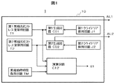
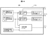
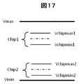
図1は、実施例1に係る半導体装置を説明するための図である。半導体装置1は累積劣化ストレス検出回路10を備える。累積劣化ストレス検出回路10は、第1の累積劣化ストレスカウント値を保持する回路(第1回路、第1累積劣化ストレス量保持回路)T1と、第1のクライテリア(判定基準)のカウント値を保持する回路(第1クライテリア保持回路)J1と、累積ストレスアラーム信号AL1を生成する回路(第1生成回路)C01と、を有する。累積ストレスアラーム信号AL1を生成する回路C01は、第1の累積劣化ストレスカウント値と第1のクライテリアのカウント値とを比較して、累積ストレスアラーム信号AL1を生成する。累積劣化ストレス検出回路10は、さらに、第2の累積劣化ストレスカウント値を保持する回路(第2回路、第2累積劣化ストレス量保持回路)T2と、第2のクライテリア(判定基準)のカウント値を保持する回路(第2クライテリア保持回路)J2と、累積ストレスアラーム信号AL2を生成する回路(第2生成回路)C02と、を有する。累積ストレスアラーム信号AL2を生成する回路C02は、第2の累積劣化ストレスカウント値と第2のクライテリアのカウント値とを比較して、累積ストレスアラーム信号AL2を生成する。
FIG. 1 is a diagram for explaining the semiconductor device according to the first embodiment. The
累積劣化ストレス検出回路10は、さらに、半導体装置1の累積動作時間のカウント値ないしはそれに相当する値を保持する回路(第3回路、累積動作時間保持回路)TMと、第1および第2の累積劣化ストレスカウント値と累積動作時間のカウント値ないしはそれに相当する値とを受ける回路(第4回路ないし演算手段、演算回路)C12と、を有する。演算回路C12は、第1および第2の累積劣化ストレスカウント値および累積動作時間のカウント値に基づいて、所望の演算を行い、演算結果として信号S1を生成する。
The accumulated degradation
第1および第2累積劣化ストレス量保持回路T1、T2のカウント値が所定値以上に達したら第1および第2生成回路C01、C02はアラーム信号AL1、AL2を出力する。半導体装置1は一つの半導体チップ(半導体基板)で形成されるが、それに限定されるものではない。第1および第2生成回路(C01、C02)、第1および第2クライテリア保持回路(J1、J2)、および、演算回路C12は、半導体装置1にハードウェア回路として構成されても良いし、半導体装置1に設けられた、例えば、中央処理装置CPUによりソフトウェアにより構成されても良い。あるいは、半導体装置1に接続された外部のデータ処理装置またはサーバ等で実現しても良い。
When the count values of the first and second cumulative deterioration stress amount holding circuits T1, T2 reach a predetermined value or more, the first and second generation circuits C01, C02 output alarm signals AL1, AL2. The
第1累積劣化ストレス量保持回路T1は、温度依存性Ea1の第1の劣化因子(摩耗故障因子)の摩耗故障度評価を行うために設けられており、温度Tがほぼ一定とみなせる所定期間のカウント数Cnt1がexp(-Ea1/kT)に比例するように構成される。カウント数Cnt1は、Cnt1=C1*exp(-Ea1/kT)で表される。ここで、C1はカウント数の温度依存性に係わる定数である。 The first cumulative deterioration stress amount holding circuit T1 is provided for evaluating the wear failure degree of the first deterioration factor (wear failure factor) of the temperature dependency Ea1, and has a predetermined period during which the temperature T can be regarded as substantially constant. The count number Cnt1 is configured to be proportional to exp (−Ea1 / kT). The count number Cnt1 is represented by Cnt1 = C1 * exp (−Ea1 / kT). Here, C1 is a constant related to the temperature dependence of the count number.
第2累積劣化ストレス量保持回路T2は、温度依存性Ea2の第2の劣化因子(摩耗故障因子)の摩耗故障度評価を行うために設けられており、温度Tがほぼ一定とみなせる所定期間のカウント数Cnt2がexp(-Ea2/kT)に比例するように構成される。カウント数Cnt2は、Cnt2=C2*exp(-Ea2/kT)で表される。ここで、C2はカウント数の温度依存性に係わる定数である。また、温度依存性Ea2は、Ea2=q2*Ea1と表現できる。 The second cumulative deterioration stress amount holding circuit T2 is provided for evaluating the wear failure degree of the second deterioration factor (wear failure factor) of the temperature dependency Ea2, and has a predetermined period during which the temperature T can be regarded as substantially constant. The count number Cnt2 is configured to be proportional to exp (−Ea2 / kT). The count number Cnt2 is represented by Cnt2 = C2 * exp (−Ea2 / kT). Here, C2 is a constant related to the temperature dependence of the count number. The temperature dependency Ea2 can be expressed as Ea2 = q2 * Ea1.
累積動作時間保持回路TMは、第1および第2累積劣化ストレス量保持回路T1、T2の累積カウント時間、あるいは相当値を保持する。相当値とは、たとえば、カウント動作を単位カウント動作(温度がほぼ一定とみなせる所定周期の期間のカウント動作)に区切った場合の累積実施回数の値Nである。以下では、値Nを用いて説明を行うが、累積カウント時間ならば、N*「一回の単位カウント動作時間」で表現できる。あるいは、間欠的に、第1および第2累積劣化ストレス量保持回路T1、T2に設けられた累積ストレスカウンタによりカウント値Cnt1、Cnt2を取得する構成において、間欠的なカウント動作の累積実施回数の値Nである。なお、間欠動作の場合には、累積カウント時間が累積ストレス時間に等しくない点も留意する必要があるが、この比は設計時に判明しているので補正可能である。本開示の趣旨に沿って、値Nと同等の別の値を用いても良い。 The accumulated operation time holding circuit TM holds the accumulated count time of the first and second accumulated deterioration stress amount holding circuits T1, T2, or an equivalent value. The equivalent value is, for example, the value N of the cumulative number of executions when the count operation is divided into unit count operations (a count operation during a predetermined period in which the temperature can be regarded as substantially constant). In the following, description will be made using the value N, but if the accumulated count time, it can be expressed by N * "one unit count operation time". Alternatively, in the configuration in which the count values Cnt1 and Cnt2 are acquired intermittently by the cumulative stress counter provided in the first and second cumulative deterioration stress amount holding circuits T1 and T2, the value of the cumulative count of the intermittent count operation is obtained. N. It should be noted that in the case of intermittent operation, the cumulative count time is not equal to the cumulative stress time, but this ratio is known at the time of design and can be corrected. Another value equivalent to the value N may be used in accordance with the spirit of the present disclosure.
<実施例1の実施の形態1>
図2は、図1の演算回路C12の構成例を示す。演算回路C12Aは第3累積劣化ストレス量保持回路(仮想)T3を有する。この場合、半導体装置1には、さらに、第3生成回路C03と第3クライテリア保持回路J3とが設けられる。
<
FIG. 2 shows a configuration example of the arithmetic circuit C12 of FIG. The arithmetic circuit C12A has a third cumulative deterioration stress amount holding circuit (virtual) T3. In this case, the
第3累積劣化ストレス量保持回路(仮想)T3は、温度依存性Ea1、温度依存性Ea2とは異なる温度依存性Ea3(Ea3=q*Ea1)の第3の摩耗故障因子(劣化因子)の仮想累積劣化ストレスカウント値を計算する。この仮想累積劣化ストレスカウント値は、第1累積劣化ストレス量保持回路T1の累積値(累積劣化ストレスカウント値)であるカウント数Cnt1の累積値、第2累積劣化ストレス量保持回路T2の累積値(累積劣化ストレスカウント値)であるカウント数Cnt2の累積値、および、累積動作時間保持回路TMの値Nの実測値に基づいて計算される。具体的な計算方法の例は、後述する図9A−図9F,図10A、図10B、図11A−図11Fにより説明される。 The third cumulative deterioration stress amount holding circuit (virtual) T3 is a virtual third of the wear failure factor (deterioration factor) having a temperature dependency Ea1 and a temperature dependency Ea3 (Ea3 = q * Ea1) different from the temperature dependency Ea2. Calculate the cumulative degradation stress count value. This virtual cumulative deterioration stress count value is the cumulative value of the count number Cnt1, which is the cumulative value (cumulative deterioration stress count value) of the first cumulative deterioration stress amount holding circuit T1, and the cumulative value of the second cumulative deterioration stress amount holding circuit T2 ( It is calculated based on the cumulative value of the count number Cnt2 that is the cumulative deterioration stress count value) and the measured value of the value N of the cumulative operation time holding circuit TM. Specific examples of the calculation method will be described with reference to FIGS. 9A to 9F, 10A, 10B, and 11A to 11F described later.
第3クライテリア保持回路J3は、温度依存性Ea3の第3の劣化因子(摩耗故障因子)の摩耗故障クライテリア(判定基準)のカウント値を保持する回路である。第3生成回路C03は、第3の仮想累積劣化ストレスカウント値と第3のクライテリアのカウント値とを比較し、累積ストレスアラーム信号AL3を生成する。第3累積劣化ストレス量保持回路T3のカウント値が所定値以上に達したら第3生成回路C03はアラーム信号AL3を出力する。図2では、第3生成回路C03および第3クライテリア保持回路J3は、演算回路C12Aの外に設けているが、演算回路C12Aの内部に設けられても良い。また、本発明の主旨に鑑みれば、T3を含むCA12,CO3,J3は同等の機能をソフトウェアで実現するのが好適である。 The third criterion holding circuit J3 is a circuit that holds the count value of the wear failure criteria (determination criterion) of the third deterioration factor (wear failure factor) of the temperature dependency Ea3. The third generation circuit C03 compares the third virtual cumulative deterioration stress count value with the third criterion count value, and generates a cumulative stress alarm signal AL3. When the count value of the third cumulative deterioration stress amount holding circuit T3 reaches a predetermined value or more, the third generation circuit C03 outputs an alarm signal AL3. In FIG. 2, the third generation circuit C03 and the third criterion holding circuit J3 are provided outside the arithmetic circuit C12A, but may be provided inside the arithmetic circuit C12A. Further, in view of the gist of the present invention, it is preferable that CA12, CO3, and J3 including T3 realize equivalent functions by software.
図2によれば、実測した温度依存性Ea1の第1劣化因子と実測した温度依存性Ea2の第2劣化因子とは異なる温度依存性Ea3を持つ第3の劣化因子の累積劣化ストレスカウント値を計算し、第3の劣化因子が摩耗故障クライテリアに達したことを判定することができる。したがって、設計時に想定していた第1及び第2の劣化因子と異なる、第3の劣化因子が後で懸念された場合でも、第3の劣化因子に対する摩耗故障危険度を判定できる半導体装置が得られる。 According to FIG. 2, the cumulative deterioration stress count value of the third deterioration factor having the temperature dependency Ea3 different from the first deterioration factor of the actually measured temperature dependency Ea1 and the second deterioration factor of the actually measured temperature dependency Ea2 is obtained. It can be calculated and determined that the third degradation factor has reached the wear failure criteria. Therefore, a semiconductor device capable of determining the degree of wear failure risk for the third deterioration factor even when there is a concern about the third deterioration factor, which is different from the first and second deterioration factors assumed at the time of design, is obtained. It is done.
<実施例1の実施の形態2>
図3は、図1の演算回路C12の他の構成例を示す。演算回路C12Bは、妥当性を判断するための回路(妥当性判定回路)AJ1を有する。妥当性判定回路AJ1は、第1累積劣化ストレス量保持回路T1の累積値(累積劣化ストレスカウント値)であるカウント数Cnt1の累積値と第2累積劣化ストレス量保持回路T2の累積値(累積劣化ストレスカウント値)であるカウント数Cnt2の累積値との相互関係指標Kq2を算出する。以下では、カウント数Cnt1の累積値をCnt1累積値と表し、カウント数Cnt2の累積値をCnt2累積値と表すものとする。相互関係指標Kq2は、第1累積劣化ストレス量保持回路T1のCnt1累積値、第2累積劣化ストレス量保持回路T2のCnt2累積値、および、累積動作時間保持回路TMの値Nの実測値に基づいて計算される。相互関係指標Kq2が所定範囲内にあるか否かに基づいて、Cnt1累積値及びCnt2累積値が妥当な実測値であるかを判定する。判定結果は、信号S1として出力される。ここで、q2=Ea2/Ea1である。
<
FIG. 3 shows another configuration example of the arithmetic circuit C12 of FIG. The arithmetic circuit C12B includes a circuit (a validity determination circuit) AJ1 for determining validity. The validity determination circuit AJ1 includes a cumulative value of the count number Cnt1, which is a cumulative value (cumulative deterioration stress count value) of the first cumulative deterioration stress amount holding circuit T1, and a cumulative value (cumulative deterioration) of the second cumulative deterioration stress amount holding circuit T2. The correlation index K q2 with the cumulative value of the count number Cnt2 that is the stress count value) is calculated. Hereinafter, the cumulative value of the count number Cnt1 is represented as a Cnt1 cumulative value, and the cumulative value of the count number Cnt2 is represented as a Cnt2 cumulative value. The correlation index K q2 is a measured value of the Cnt1 cumulative value of the first cumulative deterioration stress amount holding circuit T1, the Cnt2 cumulative value of the second cumulative deterioration stress amount holding circuit T2, and the value N of the cumulative operation time holding circuit TM. Calculated based on. Correlation index K q2 is based on whether it is within a predetermined range, determines Cnt1 accumulated value and Cnt2 accumulated value is a valid measured value. The determination result is output as a signal S1. Here, q2 = Ea2 / Ea1.
相互関係指標Kq2は、たとえば、以下の式(3)で与えられる。 The correlation index K q2 is given by the following equation (3), for example.
Kq2 = (Cnt2累積値) / {(Cnt1累積値)q2 / Nq2-1} (3)
ここで、Nは単位カウント動作(温度がほぼ一定とみなせる所定周期の期間のカウント動作)の累積実施回数であって、TMの実測値である。
K q2 = (Cnt2 cumulative value) / {(Cnt1 cumulative value) q2 / N q2-1 } (3)
Here, N is the cumulative number of executions of the unit count operation (the count operation during a predetermined period in which the temperature can be regarded as substantially constant), and is an actual measurement value of TM.
相互関係指標Kq2の妥当性は、たとえば、以下の式(4)で判定される。 The validity of the correlation index K q2 is determined by the following equation (4), for example.
(C2/C1q2) ≦ Kq2 ≦ Aq2*(C2/C1q2) (4)
ここで、C1、 C2はカウント数の温度依存性に係わる定数であって、Cnt1 = C1*exp(-Ea1/kT)、Cnt2 = C2*exp(-Ea2/kT)である。Aq2は、半導体装置に想定される温度プロファイルの範囲で最も温度変動が激しい状態に基づいて、q2=Ea2/Ea1に対してあらかじめ定めることが可能な定数である。この時、Cnt2とCnt1との間には、以下の式(5)の関係がある。
(C2 / C1 q2 ) ≤ K q2 ≤ A q2 * (C2 / C1 q2 ) (4)
Here, C1 and C2 are constants related to the temperature dependence of the count number, and Cnt1 = C1 * exp (−Ea1 / kT) and Cnt2 = C2 * exp (−Ea2 / kT). A q2 is a constant that can be determined in advance for q2 = Ea2 / Ea1 based on a state in which the temperature variation is most severe in the temperature profile range assumed for the semiconductor device. At this time, there is a relationship of the following formula (5) between Cnt2 and Cnt1.
Cnt2 = C2*exp(-Ea2/kT) = C2*{exp(-Ea1/kT)}q2 = (C2/C1q2)*(Cnt1)q2 (5)
上記式(3)の相互関係指標Kq2及び上記式(4)の判定式は、カウント値Cnt1を累積後にq2乗した値と、カウント値Cnt1をq2乗した値を累積した値との関係に関わり、後述する検討から導かれたものである。たとえば、q2=2の場合、式(4)の定数Aq2を4とするなど、q2の値に応じた定数Aq2をあらかじめ設定しておくことができる。この事は、後に示される。
Cnt2 = C2 * exp (-Ea2 / kT) = C2 * {exp (-Ea1 / kT)} q2 = (C2 / C1 q2 ) * (Cnt1) q2 (5)
The correlation index K q2 in the above formula (3) and the judgment formula in the above formula (4) are the relationship between the value obtained by accumulating the count value Cnt1 and the value obtained by accumulating the value obtained by raising the count value Cnt1 to the q2 power. Involved and derived from the discussion below. For example, in the case of q2 = 2, the constant A q2 according to the value of q2 can be set in advance, for example, the constant A q2 of Equation (4) is set to 4. This will be shown later.
図3によれば、実測した第1累積劣化ストレス量保持回路T1及び第2累積劣化ストレス量保持回路T2のカウント値のいずれかに異常が発生した場合、上記式(4)に基づき異常を検知できる。そのため、たとえば、その単位カウント動作の特定回数niで得られたカウント値を破棄して、累積値に異常値が加算されないようにすることで、信頼性の高い累積劣化ストレスカウント値が得られる。あるいは、摩耗故障クライテリアに第1累積劣化ストレス量保持回路T1または第2累積劣化ストレス量保持回路T2のいずれかが達した時点で、上記式(4)に基づき第1累積劣化ストレス量保持回路T1及び第2累積劣化ストレス量保持回路T2の累積ストレスカウント値がいずれも妥当であることを判定し、確信をもって摩耗故障の危険が高まっていることを認識できる。 According to FIG. 3, when an abnormality occurs in any of the count values of the actually measured first cumulative deterioration stress amount holding circuit T1 and second cumulative deterioration stress amount holding circuit T2, the abnormality is detected based on the above equation (4). it can. Therefore, for example, by discarding the count value obtained at the specific number of times ni of the unit count operation and preventing the abnormal value from being added to the accumulated value, a highly reliable accumulated deterioration stress count value can be obtained. Alternatively, when either the first cumulative deterioration stress amount holding circuit T1 or the second cumulative deterioration stress amount holding circuit T2 reaches the wear failure criteria, the first cumulative deterioration stress amount holding circuit T1 based on the above equation (4). And it can be recognized that the cumulative stress count value of the second cumulative deterioration stress amount holding circuit T2 is appropriate, and it can be recognized with certainty that the risk of wear failure is increasing.
次に、図1の第1累積劣化ストレス量保持回路T1、第2累積劣化ストレス量保持回路T2および累積動作時間保持回路TMを実現するためのより具体的な構成例を、図4A、図4B,図4C、図5、図6に示す。 Next, more specific configuration examples for realizing the first cumulative deterioration stress amount holding circuit T1, the second cumulative deterioration stress amount holding circuit T2, and the cumulative operation time holding circuit TM of FIG. 1 are shown in FIGS. 4A and 4B. , FIG. 4C, FIG. 5 and FIG.
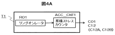
<実施例1の具体的な構成例1>
図4Aは、図1の第1累積劣化ストレス量保持回路T1の構成例を示す。第1累積劣化ストレス量保持回路T1は、リングオシレータRO1と累積ストレスカウンタACC_CNT1とを有する。exp(-Ea1/kT)に比例した周波数特性を有するリングオシレータRO1の発振が累積ストレスカウンタACC_CNT1によりカウントされる。リングオシレータRO1の発振周波数は1秒間の発振カウントである。累積ストレスカウンタACC_CNT1の出力は、第1生成回路C01および演算回路(C12、C12A、C12B)の入力に接続される。
<Specific Configuration Example 1 of Example 1>
FIG. 4A shows a configuration example of the first cumulative deterioration stress amount holding circuit T1 in FIG. The first cumulative deterioration stress amount holding circuit T1 includes a ring oscillator RO1 and a cumulative stress counter ACC_CNT1. Oscillation of the ring oscillator RO1 having a frequency characteristic proportional to exp (−Ea1 / kT) is counted by the cumulative stress counter ACC_CNT1. The oscillation frequency of the ring oscillator RO1 is an oscillation count for 1 second. The output of the cumulative stress counter ACC_CNT1 is connected to the inputs of the first generation circuit C01 and the arithmetic circuits (C12, C12A, C12B).
図4Bは、図1の第2累積劣化ストレス量保持回路T2の構成例を示す。第2累積劣化ストレス量保持回路T2は、リングオシレータRO2と累積ストレスカウンタACC_CNT2とを有する。exp(-Ea2/kT)に比例した周波数特性を有するリングオシレータRO2の発振が累積ストレスカウンタACC_CNT2によりカウントされる。リングオシレータRO2の発振周波数は1秒間の発振カウントである。累積ストレスカウンタACC_CNT2の出力は、第1生成回路C02および演算回路(C12、C12A、C12B)の入力に接続される。 FIG. 4B shows a configuration example of the second cumulative deterioration stress amount holding circuit T2 of FIG. The second cumulative deterioration stress amount holding circuit T2 includes a ring oscillator RO2 and a cumulative stress counter ACC_CNT2. Oscillation of the ring oscillator RO2 having a frequency characteristic proportional to exp (−Ea2 / kT) is counted by the cumulative stress counter ACC_CNT2. The oscillation frequency of the ring oscillator RO2 is an oscillation count for 1 second. The output of the cumulative stress counter ACC_CNT2 is connected to the inputs of the first generation circuit C02 and the arithmetic circuits (C12, C12A, C12B).
図4Cは、図1の累積動作時間保持回路TMの構成例を示す。累積動作時間保持回路TMはタイマTM1と累積時間保持回路HL1とを有する。累積時間保持回路HL1は、タイマTM1の出力を入力とし、それを保持する。累積時間保持回路HL1は、第1および第2累積劣化ストレス量保持回路T1、T2に設けられた累積ストレスカウンタACC_CNT1,ACC_CNT2の累積カウント時間、あるいは、その相当値を保持する。累積時間保持回路HL1の出力は、演算回路(C12、C12A、C12B)の入力に接続される。 FIG. 4C shows a configuration example of the cumulative operation time holding circuit TM of FIG. The accumulated operation time holding circuit TM has a timer TM1 and an accumulated time holding circuit HL1. The accumulated time holding circuit HL1 receives the output of the timer TM1 and holds it. The accumulated time holding circuit HL1 holds the accumulated count time of the accumulated stress counters ACC_CNT1 and ACC_CNT2 provided in the first and second accumulated deterioration stress amount holding circuits T1 and T2, or an equivalent value thereof. The output of the accumulated time holding circuit HL1 is connected to the input of the arithmetic circuit (C12, C12A, C12B).
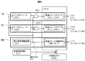
<実施例1の具体的な構成例2>
図5は、図1の第1累積劣化ストレス量保持回路T1、第2累積劣化ストレス量保持回路T2および累積動作時間保持回路TMの他の構成例を示す。なお、図5のリングオシレータ(RO1、RO2)、累積ストレスカウンタ(ACC_CNT1、ACC_CNT2)は、図4A、図4Bおよびその説明で示されたものと同じである。図4A、図4B,図4Cと異なる部分が以下に説明される。
<Specific Configuration Example 2 of Example 1>
FIG. 5 shows another configuration example of the first cumulative deterioration stress amount holding circuit T1, the second cumulative deterioration stress amount holding circuit T2, and the cumulative operation time holding circuit TM of FIG. Note that the ring oscillators (RO1, RO2) and the cumulative stress counters (ACC_CNT1, ACC_CNT2) in FIG. 5 are the same as those shown in FIGS. 4A and 4B and the description thereof. Differences from FIGS. 4A, 4B, and 4C will be described below.
図5において、累積動作時間保持回路TMは、間欠動作制御回路IOC1と累積カウント時間保持回路HL11とを有する。間欠動作制御回路IOC1から出力される動作信号AOのハイレベルに基づき、間欠カウント動作期間においてのみ、リングオシレータ(RO1、RO2)は発振動作を行う。動作信号AOのハイレベルは累積劣化ストレス検出回路10の間欠動作または間欠動作期間を指示し、動作信号AOのロウレベルは累積劣化ストレス検出回路10の非動作または非動作期間を示す。累積ストレスカウンタ(ACC_CNT1、ACC_CNT2)は、動作信号により制御されるアンド回路AN1,AN2により、その間欠カウント動作期間においてリングオシレータ(RO1、RO2)の発振を入力され、それをカウントする。累積カウント時間保持回路HL11は間欠カウント動作の回数をカウントし、カウント値として累積実施回数Nを保持する。劣化の累積量の観点から、適当な時間間隔でリングオシレータ(RO1、RO2)の発振をモニタリングしても、温度変化に対して十分な精度が得られる。そのため、間欠動作制御回路IOC1により、累積劣化ストレス検出回路10の摩耗故障の予測精度を損なうことなく、累積劣化ストレス検出回路10の消費電力および半導体装置1の全体としての消費電力を低減することができる。
In FIG. 5, the accumulated operation time holding circuit TM has an intermittent operation control circuit IOC1 and an accumulated count time holding circuit HL11. Based on the high level of the operation signal AO output from the intermittent operation control circuit IOC1, the ring oscillators (RO1, RO2) perform an oscillation operation only during the intermittent count operation period. The high level of the operation signal AO indicates an intermittent operation or an intermittent operation period of the cumulative deterioration
<実施例1の具体的な構成例3>
図6は、図5の第1累積劣化ストレス量保持回路T1、第2累積劣化ストレス量保持回路T2および累積動作時間保持回路TMの他の構成例を示す。図5と異なる部分が以下に説明される。
<Specific Configuration Example 3 of Example 1>
FIG. 6 shows another configuration example of the first cumulative deterioration stress amount holding circuit T1, the second cumulative deterioration stress amount holding circuit T2, and the cumulative operation time holding circuit TM of FIG. A different part from FIG. 5 is demonstrated below.
累積ストレスカウンタ(ACC_CNT1、ACC_CNT2)および累積カウント時間保持回路HL11の保持するカウント値を不揮発メモリNVMに退避する退避制御回路SCTを、さらに、有する。不揮発メモリNVMは、フラッシュメモリを利用することが出来る。フラッシュメモリは、半導体装置1の電源電圧の切断ないし遮断や半導体装置1のリセット動作によっても、その記憶データは保持される。劣化の累積量(累積されたカウント値)を保持するためには、累積ストレスカウンタ(ACC_CNT1、ACC_CNT2)および累積カウント時間保持回路HL11の保持するカウント値が半導体装置1の電源電圧の切断ないし遮断や半導体装置1のリセット動作により失われてはならない。半導体装置1が市場に出荷されてから製品寿命を終えるまで、累積劣化ストレス検出回路10は累積し続ける必要がある。累積ストレスカウンタ(ACC_CNT1、ACC_CNT2)および累積カウント時間保持回路HL11を電池によりバックアップされた常時電源電位の印加された半導体領域に形成しても良い。図6の様に、不揮発メモリNVMへの退避を制御する回路(退避制御回路)SCTを半導体装置1に付加すれば、累積ストレスカウンタ(ACC_CNT1、ACC_CNT2)および累積カウント時間保持回路HL11を通常のロジック領域に形成することができる。通常のロジック領域とは、ロジック回路や論理回路が形成される半導体領域であり、半導体装置1の電源電位の切断ないし遮断や半導体装置1のリセット動作により、電源電位の供給が切断ないし遮断される半導体領域を示している。カウンタアレイCNTAは、ロジック領域内における累積ストレスカウンタ(ACC_CNT1、ACC_CNT2)および累積カウント時間保持回路HL11の形成領域を表している。
There is further provided a saving control circuit SCT for saving the count values held by the cumulative stress counters (ACC_CNT1, ACC_CNT2) and the cumulative count time holding circuit HL11 to the nonvolatile memory NVM. The nonvolatile memory NVM can use a flash memory. The flash memory retains the stored data even when the power supply voltage of the
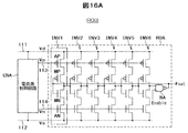
<リングオシレータ>
図7は、リングオシレータの構成を示す回路図である。図7のリングオシレータROSは、図4A、図4B、図5、図6に示されるリングオシレータRO1,RO2に利用可能である。リングオシレータROSは、摩耗故障因子の寿命τ(T)の逆数(exp(-Ea/kT))に比例した周波数特性を有する。リングオシレータROSは、電圧依存性が小さく、温度依存性が大きい、例えば、エレクトロマイグレーションやストレスマイグレーションの摩耗故障因子の累積劣化ストレス量を、リングオシレータROSの発振周波数から得ることができる。リングオシレータROSではPMOSトランジスタ(QP21)のオフ電流に比例した発振周波数を実現している。
<Ring oscillator>
FIG. 7 is a circuit diagram showing the configuration of the ring oscillator. The ring oscillator ROS of FIG. 7 can be used for the ring oscillators RO1 and RO2 shown in FIGS. 4A, 4B, 5, and 6. The ring oscillator ROS has a frequency characteristic proportional to the reciprocal (exp (−Ea / kT)) of the lifetime τ (T) of the wear failure factor. The ring oscillator ROS has a small voltage dependency and a large temperature dependency. For example, the cumulative deterioration stress amount of wear failure factors of electromigration and stress migration can be obtained from the oscillation frequency of the ring oscillator ROS. The ring oscillator ROS realizes an oscillation frequency proportional to the off current of the PMOS transistor (QP21).
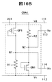
リングオシレータROSは、遅延回路DLと、安定化回路STと、インバータ遅延段INV20と、を備える。遅延回路DLはPMOSトランジスタQP21とNMOSトランジスタQN21、QN22とを有する。安定化回路STは、基準電圧(Vref)を生成するNMOSトランジスタQN23、QN24と、比較器CMPと、を備える。インバータ遅延段INV20はインバータINV21、INV22、INV23、INV24を備える。 The ring oscillator ROS includes a delay circuit DL, a stabilization circuit ST, and an inverter delay stage INV20. The delay circuit DL includes a PMOS transistor QP21 and NMOS transistors QN21 and QN22. The stabilization circuit ST includes NMOS transistors QN23 and QN24 that generate a reference voltage (Vref), and a comparator CMP. The inverter delay stage INV20 includes inverters INV21, INV22, INV23, and INV24.
動作を以下に説明する。リセット信号(reset)がハイレベルになるとノードN21はロウレベルにリセットされる。Vrefはハイレベル(Vd)とロウレベル(Vs)との中間電位であり、比較器(差動アンプ)CMPの出力のノードN22はロウレベルとなる。その結果、ノードN23はロウレベルとなり、ノードN21はresetがロウレベルに戻った後にはロウレベルのフローティング状態となる。NMOSトランジスタQN21及びQN22のしきい値電圧絶対値はPMOSトランジスタQP21のしきい値電圧絶対値より大きく設定すると、PMOSトランジスタQP21のオフリーク電流が支配的であり、ノードN21の電位はロウレベルからハイレベルに向かって徐々に上昇する。PMOSトランジスタQP21はリーク型プルアップ素子である。ノードN21の電位がVref以上になると、AMP比較器CMPの出力のノードN22はロウレベルからハイレベルに変化して、インバータ遅延段INV20(4段のインバータINV21〜INV24)の遅延の後、ノードN23はハイレベルとなる。この結果、ノードN21はロウレベルに戻る。これを繰り返して発振する。 The operation will be described below. When the reset signal (reset) becomes high level, the node N21 is reset to low level. Vref is an intermediate potential between the high level (Vd) and the low level (Vs), and the output node N22 of the comparator (differential amplifier) CMP is at the low level. As a result, the node N23 becomes low level, and the node N21 becomes a low level floating state after reset returns to the low level. When the threshold voltage absolute value of the NMOS transistors QN21 and QN22 is set larger than the threshold voltage absolute value of the PMOS transistor QP21, the off-leakage current of the PMOS transistor QP21 is dominant, and the potential of the node N21 is changed from the low level to the high level. Ascending gradually. The PMOS transistor QP21 is a leak type pull-up element. When the potential of the node N21 becomes equal to or higher than Vref, the node N22 of the output of the AMP comparator CMP changes from the low level to the high level, and after the delay of the inverter delay stage INV20 (four-stage inverters INV21 to INV24), the node N23 Become high level. As a result, the node N21 returns to the low level. It repeats this and oscillates.
ノードN21がロウレベルになってからハイレベルに遷移して再びロウレベルに戻るまでの時間は、PMOSトランジスタQP21のオフリーク電流でノードN21の電位がロウレベルからVrefまで上昇する時間(t1)と、ノードN22がハイレベルとなりインバータ遅延段INV20の遅延によりノードN21がハイレベルとなるまでの時間(t2)との和にほぼ等しい。さらに言えば、t1>>t2なので、発振周波数はPMOSトランジスタQP21のオフリーク電流にほぼ比例する。オフリーク電流は温度の逆数の指数(exp(−1/T))に依存するので、摩耗故障因子と同様な大きな温度依存性を有するリングオシレータを実現できる。 The time from the transition of the node N21 to the low level to the transition to the high level and the return to the low level again is the time (t1) when the potential of the node N21 rises from the low level to Vref due to the off-leakage current of the PMOS transistor QP21. This is approximately equal to the sum of the time (t2) until the node N21 becomes high level due to the delay of the inverter delay stage INV20. Furthermore, since t1 >> t2, the oscillation frequency is substantially proportional to the off-leakage current of the PMOS transistor QP21. Since the off-leakage current depends on the exponent of the reciprocal temperature (exp (−1 / T)), a ring oscillator having a large temperature dependence similar to the wear failure factor can be realized.
なお、図7に示すように、ノードN21を通常の論理回路ではなく比較器CMPで受けることにより安定して発振動作する効果が得られる。すなわち、ノードN21のロウレベルからハイレベルへの変化は非常に緩やかであるため、論理回路で受けた場合、その論理しきい値前後の変化がフル振幅することなく伝搬し、十分フル振幅することなく論理しきい値付近に安定してしまう場合がある。比較器CMPの出力は、その入力しきい値前後で大きくロウレベルからハイレベルへ変化するので、安定してフル振幅で発振するリングオシレータが得られる。なお、インバータIV22の出力と入力との間に耐ノイズフィードバック素子ANFが挿入されている。耐ノイズフィードバック素子ANFはPMOSトランジスタQP22、QP23、NMOSトランジスタQN25、QN26で構成されるインバータである。 As shown in FIG. 7, the effect of stable oscillation operation can be obtained by receiving the node N21 not by a normal logic circuit but by the comparator CMP. That is, since the change from the low level to the high level of the node N21 is very gradual, when it is received by the logic circuit, the change before and after the logic threshold value propagates without full amplitude and without sufficiently full amplitude. It may become stable near the logic threshold. Since the output of the comparator CMP largely changes from the low level to the high level before and after the input threshold value, a ring oscillator that stably oscillates at full amplitude can be obtained. Note that a noise-resistant feedback element ANF is inserted between the output and input of the inverter IV22. The anti-noise feedback element ANF is an inverter composed of PMOS transistors QP22 and QP23 and NMOS transistors QN25 and QN26.
<システムの全体構成の概略図>
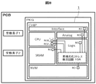
図8は、図1の半導体装置を利用したシステムの全体構成の概略図である。半導体装置1は半導体チップCHIPに形成される。半導体チップCHIPには、インターフェース回路(interface)、アナログ回路(Analog)、中央処理装置CPU、スタティックランダムアクセスメモリ(SRAM)、ロジック回路(logic)、不揮発メモリ(フラッシュメモリ)NVMなどが形成される。
<Schematic diagram of overall system configuration>
FIG. 8 is a schematic diagram of the overall configuration of a system using the semiconductor device of FIG. The
累積劣化ストレス検出回路10Aは、図1、図4A、図4B、図5、図6の累積劣化ストレス検出回路10の構成に、さらに、複数セットの累積劣化ストレス量保持回路、累積動作時間保持回路、クライテリア保持回路、生成回路、およびリングオシレータ(RO)を搭載させたものである。
The cumulative deterioration
累積劣化ストレス検出回路10A内の累積劣化ストレス量保持回路(T1、T2等)、累積動作時間保持回路(TM等)はロジック回路(logic)の形成されるロジック領域に形成される。累積劣化ストレス検出回路10A内の演算回路(C12)、クライテリア保持回路(J1、J2等)、および生成回路(C01、C02等)は同じロジック領域にハードウェア回路で実現しても良いし、CPUによるソフトウェアで実現しても良い。あるいは、半導体装置1に接続された外部のデータ処理装置またはサーバ等で実現しても良い。リングオシレータ(RO1、RO2、RO)は、図8に示されるように、異なる領域に複数設けられている。すなわち、リングオシレータ(RO1、RO2、RO)は、インターフェース回路(interface)の形成領域、アナログ回路(Analog)の形成領域、中央処理装置CPUの形成領域、スタティックランダムアクセスメモリ(SRAM)の形成領域、ロジック回路(logic) の形成領域、不揮発メモリNVMの形成領域にそれぞれ設けられる。温度上昇による摩耗劣化が懸念されるCPUの形成領域には、リングオシレータ(RO1、RO2)を近接して配置するのが良い。これにより、リングオシレータ(RO1、RO2)の温度プロファイルがほぼ同じになるようできるので、図3で説明した相互関係指標による妥当性判定の信憑性をより高めることができる。
The accumulated deterioration stress amount holding circuit (T1, T2, etc.) and the accumulated operation time holding circuit (TM etc.) in the accumulated deterioration
半導体チップCHIPはパッケージPKGに封止され、システム基板PCB上に実装される。システム基板PCB上には、抵抗素子や容量素子等の受動素子1、2も設けられる。
The semiconductor chip CHIP is sealed in a package PKG and mounted on the system board PCB.
図8に示す半導体装置1が摩耗故障の予測対象とする劣化因子としては、以下がある。
(1)参考文献に説明されている半導体チップ信頼性に関わるデバイス素子信頼性(TDDB、NBTIなど)や配線素子信頼性(EM、SMなど)。
(2)不揮発メモリNVMの情報保持保全性。
(3)パッケージPGKの信頼性に関わる半導体チップCHIPとの接続性(ワイヤボンディング、はんだボールなど)やインターポーザ劣化、封止材レジン劣化。
(4)システム基板PCBの信頼性に関わるパッケージPKGとの接続性(はんだボールなど)や半導体チップCHIP近辺の受動素子1,2の劣化。
The deterioration factors that the
(1) Device element reliability (TDDB, NBTI, etc.) and wiring element reliability (EM, SM, etc.) related to semiconductor chip reliability described in the references.
(2) Information retention integrity of the nonvolatile memory NVM.
(3) Connectivity with the semiconductor chip CHIP related to the reliability of the package PGK (wire bonding, solder balls, etc.), interposer deterioration, sealing material resin deterioration.
(4) Connectivity with the package PKG related to the reliability of the system board PCB (solder ball etc.) and deterioration of the
累積劣化ストレス検出回路10Aに、図2に示した演算回路C12Aを適用することにより、上記の様な多様な劣化因子に対する摩耗故障の予測を行うことができる。
By applying the arithmetic circuit C12A shown in FIG. 2 to the cumulative deterioration
<実施例1の実施の形態1の計算例>
次に、図2の演算回路C12Aにおける仮想累積劣化ストレスカウント値(Cnt3累積値)の計算例が示される。
<Calculation Example of
Next, a calculation example of the virtual cumulative deterioration stress count value (Cnt3 cumulative value) in the arithmetic circuit C12A of FIG. 2 is shown.
これは、温度依存性Ea3の第3の劣化因子の仮想累積劣化ストレスカウント値(Cnt3累積値)を、実測値から計算するための具体的な方法である。この実測値は、第1累積劣化ストレス量保持回路T1の累積劣化ストレスカウント値のカウント数Cnt1累積値、第2累積劣化ストレス量保持回路T2の累積劣化ストレスカウント値のカウント数Cnt2累積値、および累積動作時間保持回路TMの値Nである。温度依存性Ea3は、温度依存性Ea1、Ea2とは異なるものであり、Ea3=q*Ea1と表されるものとし、値qは定数である。以下、図9A−図9F,図10A、図10B、図11A−図11Fを用いて説明する。 This is a specific method for calculating the virtual cumulative deterioration stress count value (Cnt3 cumulative value) of the third deterioration factor of the temperature dependency Ea3 from the actually measured value. The actually measured values are the cumulative number Cnt1 of the cumulative deterioration stress count value of the first cumulative deterioration stress amount holding circuit T1, the cumulative number Cnt2 of the cumulative deterioration stress count value of the second cumulative deterioration stress amount holding circuit T2, and This is the value N of the accumulated operation time holding circuit TM. The temperature dependency Ea3 is different from the temperature dependency Ea1 and Ea2, and is expressed as Ea3 = q * Ea1, and the value q is a constant. Hereinafter, description will be made with reference to FIGS. 9A to 9F, 10A, 10B, and 11A to 11F.
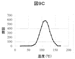
図9Aは、累積期間での半導体装置の温度の第1の確率分布を示す図である。図9Cは、累積期間での半導体装置の温度の第2の確率分布を示す図である。図9Eは、累積期間での半導体装置の温度の第3の確率分布を示す図である。横軸は温度T(℃)を示す。縦軸は、累積期間を、単位カウント動作の累積実施回数Nとし、N=5000回の場合における各温度への到達した回数で示している。図9Bは、図9Aにおける下記式(6)に定義する相互関係指標と値qとの関係を示す図である。図9Dは、図9Cにおける相互関係指標と値qとの関係を示す図である。図9Fは、図9Eにおける相互関係指標と値qとの関係を示す図である。 FIG. 9A is a diagram showing a first probability distribution of the temperature of the semiconductor device in the accumulation period. FIG. 9C is a diagram illustrating a second probability distribution of the temperature of the semiconductor device during the accumulation period. FIG. 9E is a diagram showing a third probability distribution of the temperature of the semiconductor device during the accumulation period. The horizontal axis indicates the temperature T (° C.). The vertical axis shows the cumulative period as the number of times the unit count operation has been performed N, and the number of times each temperature has been reached when N = 5000. FIG. 9B is a diagram showing the relationship between the correlation index defined in the following formula (6) in FIG. 9A and the value q. FIG. 9D is a diagram illustrating a relationship between the correlation index and the value q in FIG. 9C. FIG. 9F is a diagram showing the relationship between the correlation index and the value q in FIG. 9E.
図9A−図9Fにおいて、1回の単位カウント動作期間中、温度はほぼ一定であり、第1累積劣化ストレスカウント値は、Cnt1 = C1 * exp (-Ea1/kT)であり、仮想累積劣化ストレスカウント値は、Cnt3 = (Cnt1)q = C1q * exp(-Ea3/kT)である。また、Ea1=0.5eVとし、q=Ea3/Ea1とする。単位カウント動作の累積実施回数N=5000回において、単位カウント動作ごとに温度が図9A、図9C、図9Eの確率分布で温度が変動する場合を検討する。この時、以下の式(6)で、Cnt1累積値とCnt3累積値との相互関係指標を定義する。 9A to 9F, the temperature is substantially constant during one unit count operation period, the first cumulative deterioration stress count value is Cnt1 = C1 * exp (−Ea1 / kT), and the virtual cumulative deterioration stress count value is Cnt3 = (Cnt1) q = C1 q * exp (-Ea3 / kT). Further, Ea1 = 0.5 eV and q = Ea3 / Ea1. Consider the case where the temperature fluctuates according to the probability distributions of FIGS. 9A, 9C, and 9E for each unit count operation when the unit count operation is performed N = 5000 times. At this time, the correlation index between the Cnt1 cumulative value and the Cnt3 cumulative value is defined by the following equation (6).
Kq=(Cnt3累積値)/{(Cnt1累積値)q / Nq-1} (6)
相互関係指標Kqは図9A、図9C、図9Eの分布毎に異なり、それぞれ図9B、図9D、図9Fの様な相互関係指標Kqのシミュレーション結果になる。図9B、図9D、図9Fでは、値qの0から5までの相互関係指標Kqが示されており、値q=1の場合のCnt1累積値、および値qがq=2の場合のCnt2累積値が取得されている場合である。値qがq<1の複数点、1.5、2.5、3.5、4、4.5に対応する相互関係指標Kqの値はシミュレーション値である。
K q = (Cnt3 cumulative value) / {(Cnt1 cumulative value) q / N q-1 } (6)
Correlation index K q Figure 9A, different for each distribution in FIG. 9C, FIG. 9E, respectively Figure 9B, becomes FIG. 9D, the simulation results of the correlation index K q such as Figure 9F. In FIG. 9B, FIG. 9D, and FIG. 9F, the correlation index K q from 0 to 5 of the value q is shown. The Cnt1 cumulative value when the value q = 1, and the value q when the value q is q = 2 This is a case where the Cnt2 cumulative value has been acquired. Value q is q <1 at a plurality of points, the value of the correlation index K q corresponding to 1.5,2.5,3.5,4,4.5 is simulated value.
図9A、図9Bは、累積期間において温度変動がそれほど無い場合であり、相互関係指標Kqは、ほぼ1となる。なぜなら、一定のカウント値がN回あるとすると、(Cnt3累積値)/{(Cnt1累積値)q / Nq-1}が1となるからである。すなわち、相互関係指標Kqは、カウント動作の期間に温度変動が無い場合、すなわち、累積期間に渡って温度変動が無い場合に下記の式(7)(8)となる。 9A and 9B show a case where there is not much temperature fluctuation in the accumulation period, and the correlation index K q is almost 1. This is because (Cnt3 accumulated value) / {(Cnt1 accumulated value) q / Nq -1 } becomes 1 if there are N counts. That is, the correlation index Kq is expressed by the following equations (7) and (8) when there is no temperature fluctuation during the counting operation, that is, when there is no temperature fluctuation over the accumulation period.
Cnt3累積値 = (Cnt1)q累積値 = Cnt1Tq x N (7)
(Cnt1累積値)q = (Cnt1T x N)q = Cnt1Tq x Nq (8)
ここで、Cnt1Tはすべての単位カウント動作で同じとなるCnt1の値である。式(6)に代入すると、Kq=1である。
図9C、図9D、図9E、図9Fは、累積期間の温度変動がある場合であり、相互関係指標Kqは1以上(Kq>1)となる。相互関係指標Kqは、0<q<1ではKq=1が良い近似となる。
また、図9E、図9Fの様に、累積期間において温度変動が大きいほど、相互関係指標Kqは大きくなる。すなわち、Cnt1累積値からCnt3累積値を正確に計算することは難しい。
Cnt3 cumulative value = (Cnt1) q cumulative value = Cnt1T q x N (7)
(Cnt1 cumulative value) q = (Cnt1T x N) q = Cnt1T q x N q (8)
Here, Cnt1T is the value of Cnt1 that is the same in all unit count operations. Substituting into equation (6), K q = 1.
9C, FIG. 9D, FIG. 9E, and FIG. 9F show the case where there is a temperature variation during the accumulation period, and the correlation index K q is 1 or more (K q > 1). For the correlation index K q , K q = 1 is a good approximation when 0 <q <1.
Further, as shown in FIGS. 9E and 9F, the correlation index K q increases as the temperature variation increases in the accumulation period. That is, it is difficult to accurately calculate the Cnt3 cumulative value from the Cnt1 cumulative value.
しかしなから、温度依存性Ea1とは異なる温度依存性Ea2=q2*Ea1の温度依存性の第2の劣化因子の累積劣化ストレスカウント値(Cnt2累積値)が取得されている場合、値qが1以上q2以下の範囲(たとえばq2=2でq=1.5)であれば、相互関係指標K1=1と相互関係指標Kq2=(Cnt2累積値)/{(Cnt1累積値)q2 / Nq2-1}との内挿から高い精度で相互関係指標Kqを見積もることができる。すなわち、Cnt3累積値を精度よく見積もることができる。なお、図9ではCnt2 = (Cnt1)q2 = C1q2 * exp(-Ea2/kT)(q2=2)としてプロットしているが、式(5)のようにCnt2 = (C2/C1q2)*(Cnt1)q2が一般形であるので、実際にはCnt2累積値を(C2/C1q2)で除したCnt2_nrm累積値を相互関係指標Kq2の算出に用いる必要がある。 However, if the cumulative deterioration stress count value (Cnt2 cumulative value) of the temperature-dependent second deterioration factor of temperature dependency Ea2 = q2 * Ea1 different from the temperature dependency Ea1 is acquired, the value q is In the range of 1 to q2 (for example, q2 = 2 and q = 1.5), the correlation index K 1 = 1 and the correlation index K q2 = (Cnt2 cumulative value) / {(Cnt1 cumulative value) q2 / N q2 -1 } can be used to estimate the correlation index K q with high accuracy. That is, the Cnt3 cumulative value can be estimated with high accuracy. Incidentally, Cnt2 = (Cnt1) q2 = C1 q2 * exp (-Ea2 / kT) in FIG. 9 (q2 = 2) has been plotted as, Cnt2 = (C2 / C1 q2 ) as in equation (5) * (Cnt1) because q2 is generally shaped, in practice it is necessary to use for the calculation of the correlation index K q2 the Cnt2_nrm cumulative value obtained by dividing the Cnt2 accumulated value (C2 / C1 q2).
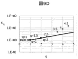
図10Aは、相互関係指標の精度を説明するための図である。図10Bは、値q2を2より大きくした場合の相互関係指標の精度を説明するための図である。 FIG. 10A is a diagram for explaining the accuracy of the correlation index. FIG. 10B is a diagram for explaining the accuracy of the correlation index when the value q2 is greater than 2.
図10Aは図9Fと同等であり、値qが1と2との間は精度よく相互関係指標Kqを見積もることができることを示している。値qが2以上の場合は、精度が悪くなる。したがって、値qとしてq=1〜2(Ea=0.5eV〜1eV)の領域の精度を重視する場合に効果がある。一方、図10Bは、図9Fにおいて、取得されているCnt2累積値を、値qが4(q2=4)の場合のカウント値とした場合を示す。図10Bでは、内挿で見積ることが可能な値qの範囲を拡大した。Cnt2累積値のq2を大きくすると、内挿の精度は低下するが、相互関係指標Kqの見積もれる値qの範囲が拡大する効果がある。 FIG. 10A is equivalent to FIG. 9F, and shows that the correlation index K q can be estimated with high accuracy when the value q is between 1 and 2. When the value q is 2 or more, the accuracy is deteriorated. Therefore, it is effective when importance is attached to the accuracy of the region of q = 1 to 2 (Ea = 0.5 eV to 1 eV) as the value q. On the other hand, FIG. 10B shows a case where the acquired Cnt2 accumulated value in FIG. 9F is a count value when the value q is 4 (q2 = 4). In FIG. 10B, the range of the value q that can be estimated by interpolation is expanded. If Cnt2 increasing the q2 of the cumulative value, the accuracy of the interpolation is reduced, the effect of a range of estimable value q interrelated index K q is enlarged.
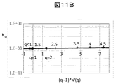
図11A、図11C,図11Eは、図9A、図9C、図9Eと同じものである。図11Bは、図9Bに示す図の横軸を、値qではなく、(q-1)*√(q)とした場合の相互関係指標Kqを説明する図である。図11Dは、図9Dに示す図の横軸を、値qではなく、(q-1)*√(q)とした場合の相互関係指標Kqを説明する図である。図11Fは、図9Fに示す図の横軸を、値qではなく、(q-1)*√(q)とした場合の相互関係指標Kqを説明する図である。図11B、図11D、図11Fのそれぞれに示されるように、横軸を(q-1)*√(q)として相互関係指標Kqをプロットすると、第1累積劣化ストレスカウント値のCnt1累積値(q=1)、 第2累積劣化ストレスカウント値のCnt2累積値(q=2)の2点から、その内挿領域だけでなく、その外挿領域についても、相互関係指標Kq、すなわち仮想累積劣化ストレスカウント値Cnt3累積値を見積もることが可能であることが示される。また、図11B、図11D、図11Fから、図11A、図11C,図11Eに示されるような異なる温度変動の確率分布の状態に対しても、q=1のCnt1累積値の実測値とq=2のCnt2累積値の実測値との外挿から、任意の値qの仮想累積劣化ストレスカウント値Cnt3累積値を精度よく見積もれることがわかる。 11A, 11C, and 11E are the same as FIGS. 9A, 9C, and 9E. FIG. 11B is a diagram for explaining the correlation index K q when the horizontal axis of the diagram shown in FIG. 9B is not (q) but (q−1) * √ (q). FIG. 11D is a diagram for explaining the correlation index K q when the horizontal axis of the diagram shown in FIG. 9D is not (q) but (q−1) * √ (q). FIG. 11F is a diagram for explaining the correlation index K q when the horizontal axis of the diagram shown in FIG. 9F is (q−1) * √ (q) instead of the value q. As shown in FIGS. 11B, 11D, and 11F, when the horizontal axis is (q-1) * √ (q) and the correlation index K q is plotted, the Cnt1 cumulative value of the first cumulative deterioration stress count value (Q = 1), the Cnt2 cumulative value (q = 2) of the second cumulative degradation stress count value, not only the interpolation area but also the extrapolation area, the correlation index K q , that is, the virtual It is shown that the cumulative deterioration stress count value Cnt3 cumulative value can be estimated. Further, from FIGS. 11B, 11D, and 11F, the measured value of the Cnt1 cumulative value of q = 1 and the qt are also obtained for the probability distribution states of different temperature fluctuations as shown in FIGS. 11A, 11C, and 11E. From the extrapolation of the Cnt2 cumulative value of = 2 to the actual measurement value, it can be seen that the virtual cumulative deterioration stress count value Cnt3 cumulative value of an arbitrary value q can be accurately estimated.
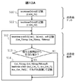
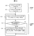
<実施例1の実施の形態1に係る実施フロー>
次に、図2に示される演算回路C12Aを用いた場合の実施フローを示す。図12Aは、実施例1の実施の形態1の全体的な実施フローである。図12Bは、図12AのステップS6の詳細な算出フローを示す。まず、前提を説明する。図9A−図9F,図10A、図10B、図11A−図11Fの説明では、第2累積劣化ストレス量保持回路T2の累積劣化ストレスカウント値のカウント数Cnt2累積値は、Cnt2 = (Cnt1)q2=C1q2*exp(-Ea2/kT)、q2=Ea2/Ea1 を前提としたものであった。しかし、実際の半導体装置1において設計される第2累積劣化ストレス量保持回路T2の累積劣化ストレスカウント値は、Cnt2 = C2*exp(Ea2/kT)であり、係数はC1q2とは異なる。その比B=C2/ C1q2を図12Aおよび図12Bでは考慮した。B値は半導体装置1の出荷前テストで取得できる。また、1回の単位カウント動作時間の代わりに、出荷前テスト時のテスト時間testtimeを時間単位とした。testtimeはその期間の温度がほぼ一定の短い期間である。実際にはtesttimeを1回の単位カウント動作時間とするのが好適である。あるいは、testtimeのカウント時間を間欠的に行うようにすると、消費電力を下げることができる。出荷前テストでは、温度Tを150℃としてテストを行うものとする。
<Implementation flow according to
Next, an implementation flow in the case of using the arithmetic circuit C12A shown in FIG. 2 is shown. FIG. 12A is an overall execution flow of the first embodiment of the first embodiment. FIG. 12B shows a detailed calculation flow of step S6 of FIG. 12A. First, the premise will be described. 9A to 9F, FIG. 10A, FIG. 10B, and FIG. 11A to FIG. 11F, the count number Cnt2 of the cumulative degradation stress count value of the second cumulative degradation stress amount holding circuit T2 is Cnt2 = (Cnt1) q2. = C1 q2 * exp (-Ea2 / kT), q2 = Ea2 / Ea1. However, the cumulative degradation stress count value of the second cumulative degradation stress amount holding circuit T2 designed in the
ステップS1およびS2は、半導体装置1の出荷前テスト時に実施される。ステップS1では、150℃、testtimeの第1累積劣化ストレス量保持回路T1のカウント値Cnt1を取得し、CntH_T1として記憶させる。ステップS2では、150℃、testtimeの第2累積劣化ストレス量保持回路T2のカウント値Cnt2を取得し、CntH_T2として記憶させる。
Steps S1 and S2 are performed during a pre-shipment test of the
ステップS3〜S6は、半導体装置1の出荷後において半導体装置1の動作時に行われる。ステップS3では、testtime x Nの第1累積劣化ストレス量保持回路T1の累積劣化ストレスカウント値Cnt1累積値を取得し、Acc_Cnt_T1として記憶させる。ステップS4では、testtime x Nの第2累積劣化ストレス量保持回路T2の累積劣化ストレスカウント値Cnt2累積値を取得し、Acc_Cnt_T2として記憶させる。ステップ5では、累積動作時間保持回路TMの単位動作の累積実施回数のカウント値Nを取得し、Acc_Cnt_TMとして記憶させる。ステップS6では、温度依存性Ea3相当の仮想累積劣化ストレスカウント値であるCnt3累積値を算出する。なお、ステップ6は毎回実施されなくても良い。
Steps S <b> 3 to S <b> 6 are performed when the
ステップS6の詳細な算出フローは、図12Bに示される。 The detailed calculation flow of step S6 is shown in FIG. 12B.
ステップS61において、test結果から、比Bを求める。比B は、B = (CntH_T2) / (CntH_T1)q2 = C2 / C1q2 である。なお、Cnt1 = C1*exp(-Ea1/kT)、Cnt2=C2*exp(-Ea2/kT)=C2*{exp(-Ea1/kT)}q2 、q2=Ea2/Ea1である。 In step S61, the ratio B is obtained from the test result. The ratio B is B = (CntH_T2) / (CntH_T1 ) q2 = C2 / C1 q2. Note that Cnt1 = C1 * exp (−Ea1 / kT), Cnt2 = C2 * exp (−Ea2 / kT) = C2 * {exp (−Ea1 / kT)} q2 , q2 = Ea2 / Ea1.
ステップS62では、規格化した第2累積劣化ストレス量保持回路T2の累積劣化ストレスカウント値Cnt2_nrmを定義し求める。なお、Cnt2_nrm=C1q2*exp(-Ea2/kT)=(Cnt1)q2、Cnt2_nrm=Cnt2 /Bなので、規格化したAcc_Cnt_T2_nrm は、Acc_Cnt_T2_nrm= Cnt2_nrm累積値=Acc_Cnt_T2 / Bである。 In step S62, a standardized cumulative degradation stress count value Cnt2_nrm of the second cumulative degradation stress amount holding circuit T2 is defined and determined. Since Cnt2_nrm = C1 q2 * exp (-Ea2 / kT) = (Cnt1) q2 and Cnt2_nrm = Cnt2 / B, the standardized Acc_Cnt_T2_nrm is Acc_Cnt_T2_nrm = Cnt2_nrm cumulative value = Acc_Cnt_T2 / B.
ステップS63では、規格化したAcc_Cnt_T2_nrmの相互関係指標Kq2をY軸に、(q-1)*√(q)をX軸に打点し、(0,1)と直線で結ぶ。Y軸は対数軸である。すなわち、図11B、図11D、図11Fの相互関係指標Kq2と(q-1)*√(q)との関係を求める。相互関係指標Kq2は、Kq2 = (Acc_Cnt_T2_nrm) / {(Acc_Cnt_T1)q2 / Nq2-1}である。 In step S63, the correlation index K q2 of Acc_Cnt_T2_nrm normalized to the Y axis, and RBI the (q-1) * √ ( q) the X-axis, connected by a straight line (0,1). The Y axis is a logarithmic axis. That is, the relationship between the correlation index K q2 and (q−1) * √ (q) in FIGS. 11B, 11D, and 11F is obtained. Correlation index K q2 is a K q2 = (Acc_Cnt_T2_nrm) / { (Acc_Cnt_T1) q2 / N q2-1}.
ステップS64では、ステップS63で求めた上記直線上で、q=Ea3/Ea1相当の相互関係指標Kqを得る。相互関係指標Kqは、Kq = (Acc_Cnt_T3_nrm) / {(Acc_Cnt_T1)q / Nq-1}である。また、規格化したAcc_Cnt_T3_nrmは、Acc_Cnt_T3_nrm= Cnt3_nrm累積値である。Cnt3_nrmは、温度依存性Ea3相当の仮想累積劣化ストレスカウント値C1q*exp(-Ea3/kT) =(Cnt1)qである。 In step S64, in the straight line in the obtained step S63, the obtaining q = Ea3 / Ea1 corresponding interrelationships index K q. Correlation index K q is K q = (Acc_Cnt_T3_nrm) / { (Acc_Cnt_T1) q / N q-1}. Also, normalized Acc_Cnt_T3_nrm is Acc_Cnt_T3_nrm = Cnt3_nrm cumulative value. Cnt3_nrm is a virtual cumulative deterioration stress count value C1 q * exp (−Ea3 / kT) = (Cnt1) q corresponding to the temperature dependence Ea3.
ステップS65では、ステップ64で求めた相互関係指標Kq、及びAcc_Cnt_T1、NとからAcc_Cnt_T3_nrmを逆算する。
In step S65, Acc_Cnt_T3_nrm is calculated backward from the correlation index K q obtained in
ステップS66では、ステップS64で定義したCnt3_nrmの150℃、 testtimeでの仮想累積劣化ストレスカウント値CntH_T3_nrmを算出する。CntH_T3_nrmは、CntH_T3_nrm=(CntH_T1)qである。
ステップS67では、得られたAcc_Cnt_T3_nrmとCntH_T3_nrmとの比が、Ea3温度依存性の劣化因子に対して、150℃相当でtesttimeの何倍の累積劣化ストレス時間に達しているかを示す。
In step S66, a virtual cumulative deterioration stress count value CntH_T3_nrm at 150 ° C. and testtime of Cnt3_nrm defined in step S64 is calculated. CntH_T3_nrm is CntH_T3_nrm = (CntH_T1) q .
In step S67, the ratio of the obtained Acc_Cnt_T3_nrm and CntH_T3_nrm is equivalent to 150 ° C. with respect to the Ea3 temperature-dependent deterioration factor and indicates how many times the accumulated deterioration stress time has reached the test time.
図12Aおよび図12Bによれば、温度依存性Ea1の第1の劣化因子の累積劣化ストレスカウント値(Cnt1累積値)、温度依存性Ea2の第2の劣化因子の累積劣化ストレスカウント値(Cnt2累積値)、及び単位カウント動作の累積実施回数Nとから、温度依存性Ea3の第3の劣化因子の仮想累積ストレスカウント値(Cnt3累積値)を見積もることができる。ずなわち、図8で説明された様な様々な劣化因子の摩耗故障を精度よく予測できる半導体装置1が得られる。なお、図12では図11相当で第3の劣化因子の摩耗故障を予測するフロー例を示したが、図9相当など、他のプロットでCnt1累積値及びCnt2累積値の実測からステップS64のKqを得ても良い。
According to FIGS. 12A and 12B, the cumulative degradation stress count value (Cnt1 cumulative value) of the first degradation factor of temperature dependency Ea1 and the cumulative degradation stress count value (Cnt2 accumulation of the second degradation factor of temperature dependency Ea2). Value) and the number N of cumulative executions of the unit count operation, the virtual cumulative stress count value (Cnt3 cumulative value) of the third deterioration factor of the temperature dependence Ea3 can be estimated. That is, the
<実施例1の実施の形態2の具体的な説明>
図3で示された妥当性判定回路AJ1に関し、さらに、具体的に説明する。
<Specific Description of
The validity determination circuit AJ1 shown in FIG. 3 will be described more specifically.
第1累積劣化ストレス量保持回路T1の累積値(累積劣化ストレスカウント値)Cnt1累積値と第2累積劣化ストレス量保持回路T2の累積値(累積劣化ストレスカウント値)Cnt2累積値のあるべき相互関係を以下に示す。単位カウント動作期間”i”に取得されるカウント値は、その期間が短く温度Tがほぼ一定とした場合、以下である。 The interrelationship between the cumulative value (cumulative degradation stress count value) Cnt1 of the first cumulative degradation stress amount holding circuit T1 and the cumulative value (cumulative degradation stress count value) Cnt2 of the second cumulative degradation stress amount retention circuit T2 should be Is shown below. The count value acquired in the unit count operation period “i” is as follows when the period is short and the temperature T is substantially constant.
Cnt1[i] = C1*exp(-Ea1/kT)
Cnt2[i] = C2*exp(-Ea2/kT) = C2*exp(-q2*Ea1/kT) = (C2/C1q2)*(Cnt1[i])q2
ここで、q2 = Ea2 / Ea1 である。
Cnt1 [i] = C1 * exp (-Ea1 / kT)
Cnt2 [i] = C2 * exp (-Ea2 / kT) = C2 * exp (-q2 * Ea1 / kT) = (C2 / C1 q2 ) * (Cnt1 [i]) q2
Here, q2 = Ea2 / Ea1.
もっとも単純なケースとして、N回のカウント累積期間に渡っても温度Tが一定なら、Cnt1[i]は”i"によらず同じ値Cnt1Tとなる。 In the simplest case, if the temperature T is constant over N count accumulation periods, Cnt1 [i] is the same value Cnt1T regardless of “i”.
ΣCnt1[i] = Cnt1T x N
ΣCnt2[i] = (C2/C1q2)*(Cnt1[i])q2 = (C2/C1q2)*(Cnt1T x N)q2
この時、実施例1の実施の形態1で定義したのと同じ相互関係指標Kq2は、下記である。
ΣCnt1 [i] = Cnt1T x N
ΣCnt2 [i] = (C2 / C1 q2 ) * (Cnt1 [i]) q2 = (C2 / C1 q2 ) * (Cnt1T x N) q2
At this time, the same correlation index K q2 as defined in
Kq2 = (Cnt2累積値) / {(Cnt1累積値)q2 / Nq2-1} = (C2/C1q2)
実施例1の実施の形態1では、仮想累積劣化ストレスカウント値Cnt3の係数C3を、C1qと定義したので、温度変動が無い場合、Kq=1であった。実施例1の実施の形態2では、Cnt2は温度依存性Ea2の別の累積劣化ストレスカウンタの実測値なので、独立した係数C2を有し、その結果、温度Tが一定の場合、Kq2 = (C2/C1q2)となる。
K q2 = (Cnt2 cumulative value) / {(Cnt1 cumulative value) q2 / N q2-1 } = (C2 / C1 q2 )
In
N回のカウント累積期間に渡って温度Tが変動する通常のケースでは、図9A−図9F,図10A、図10B、図11A−図11Fに示した結果から分かるように、Kq2 = Aq2 * (C2/C1q2)、 (Aq2 > 1)となり、温度依存性が大きいほどAq2は大きい。なお、図9A−図9F,図10A、図10B、図11A−図11Fでは、C2/C1q2=1の例を示しているので、これらのグラフの縦軸Kq2は前記Aq2に等しい。温度依存性が大きいほどAq2が大きいことは、q2 = 2の場合を例に、簡単な数式で理解することができる。xを変動する任意の変数、mをxの平均値とすると、以下となる。 In the normal case where the temperature T fluctuates over N count accumulation periods, as can be seen from the results shown in FIGS. 9A to 9F, 10A, 10B, and 11A to 11F, K q2 = A q2 * (C2 / C1 q2 ), (A q2 > 1), and A q2 increases as the temperature dependence increases. 9A to 9F, FIG. 10A, FIG. 10B, and FIG. 11A to FIG. 11F show examples of C2 / C1 q2 = 1, and therefore, the vertical axis K q2 of these graphs is equal to A q2 . The fact that A q2 is larger as the temperature dependence is larger can be understood by a simple mathematical expression, taking the case of q2 = 2 as an example. If x is an arbitrary variable and m is an average value of x, the following is obtained.
<x2> = m2 + <(x - m)2>
ここで、< >は囲まれた値の平均を示す。
<x 2 > = m 2 + <(x-m) 2 >
Here, <> indicates the average of the enclosed values.
この一般式を、今回の実施例1の実施の形態2の場合にあてはめると、以下となる。
When this general formula is applied to the case of
Cnt1累積値 = m * N
Cnt2累積値 = (C2/C12)*(Cnt1の2乗の累積値)= (C2/C1q2) * <x2> * N
したがって、相互関係指標K2は、以下となる。
Cnt1 cumulative value = m * N
Cnt2 cumulative value = (C2 / C1 2 ) * (Cnt1 squared cumulative value) = (C2 / C1 q2 ) * <x 2 > * N
Therefore, correlation index K 2 becomes less.
K2 = (Cnt2累積値) / {(Cnt1累積値)2 / N}
= (C2/C12) * <x2> / m2
= (C2/C12) *(1 + <(x - m)2> / m2)
ここで、<(x - m)2> / m2 > 0 である。すなわち、カウント累積期間中に温度Tが変動する場合、その変動が大きいほど、相互関係指標K2は(C2/C12)より大きくなる。言い換えれば、定数A2は1より大きくなる。
K 2 = (Cnt2 cumulative value) / {(Cnt1 cumulative value) 2 / N}
= (C2 / C1 2 ) * <x 2 > / m 2
= (C2 / C1 2 ) * (1 + <(x-m) 2 > / m 2 )
Here, <(x−m) 2 > / m 2 > 0. That is, when the temperature T fluctuates during the count accumulation period, the correlation index K 2 becomes larger than (C2 / C1 2 ) as the fluctuation increases. In other words, the constant A 2 is greater than 1.
図9A−図9Fを再び参照する。たとえば、相互関係指標K2(q=2でのKq)は、図9Bで約1.0、図9Dで約1.5、図9Fで約2.7である。現実的に半導体装置1が経験する温度プロファイルを考えた時、相互関係指標K2は最大でも4を超えないという解析結果を得た。図9A−図9FはC2/C12=1に規格化した場合であり、K2はA2に等しく、以下の範囲にあれば、Cnt1累積値、Cnt2累積値共に妥当であると判断できる。
Reference is again made to FIGS. 9A-9F. For example, the correlation index K 2 (K q when q = 2) is about 1.0 in FIG. 9B, about 1.5 in FIG. 9D, and about 2.7 in FIG. 9F. When considering the temperature profile that the
(C2/C12) ≦ K2 ≦ A2*(C2/C12)、 A2 = 4
ここでは、q2 = 2の場合について示したが、q2が2以外の場合でも、Cnt1累積値とCnt2累積値と単位カウント動作の累積実施回数Nとで計算される相互関係指標Kq2があるべき範囲を同様に定義でき、以下となる。
(C2 / C1 2 ) ≤ K 2 ≤ A 2 * (C2 / C1 2 ), A 2 = 4
Here, the case of q2 = 2 is shown, but even if q2 is other than 2, there should be an interrelation index K q2 calculated by the Cnt1 accumulated value, the Cnt2 accumulated value, and the accumulated execution count N of the unit count operation. The range can be defined in the same way:
(C2/C1q2) ≦ Kq2 ≦ Aq2*(C2/C1q2)
ここで、Aq2は、半導体装置に想定される温度プロファイルの範囲で最も温度変動が激しい状態に基づいて、q2 = Ea2 / Ea1に対してあらかじめ定めることが可能な定数である。
(C2 / C1 q2 ) ≤ K q2 ≤ A q2 * (C2 / C1 q2 )
Here, A q2 is a constant that can be determined in advance for q2 = Ea2 / Ea1 based on a state where the temperature fluctuation is most severe in the temperature profile range assumed for the semiconductor device.
<実施例1の実施の形態2に係る実施フロー>
次に、図3に示される演算回路C12Bを用いた場合の実施フローを示す。図13Aは、実施例1の実施の形態2の全体的な実施フローである。図13Bは、図13AのステップS13の詳細な判定フローを示す。まず、前提を説明する。1回の単位カウント動作時間の代わりに、出荷前テスト時のテスト時間testtimeを時間単位とした。testtimeはその期間の温度がほぼ一定の短い期間である。出荷前テストでは、温度Tを150℃としてテストを行うものとする。
<Implementation flow according to
Next, an implementation flow when the arithmetic circuit C12B shown in FIG. 3 is used is shown. FIG. 13A is an overall execution flow of the second embodiment of the first embodiment. FIG. 13B shows a detailed determination flow in step S13 of FIG. 13A. First, the premise will be described. Instead of one unit count operation time, the test time testtime at the time of the pre-shipment test was set as a time unit. The testtime is a short period in which the temperature during that period is almost constant. In the pre-shipment test, the test is performed at a temperature T of 150 ° C.
ステップS10およびS11は、半導体装置1の出荷前テスト時に実施される。ステップS10では、150℃、testtimeの第1累積劣化ストレス量保持回路T1の累積劣化ストレスカウント値Cnt1を取得し、CntH_T1として記憶させる。ステップS11では、150℃、testtimeの第2累積劣化ストレス量保持回路T2の累積劣化ストレスカウント値Cnt2を取得し、CntH_T2として記憶させる。
Steps S10 and S11 are performed during a pre-shipment test of the
ステップS12〜S14は、半導体装置1の出荷後において半導体装置1の動作時に行われる。
Steps S12 to S14 are performed during the operation of the
ステップS12では、所定期間testtime x niの第1累積劣化ストレス量保持回路T1の累積劣化ストレスカウント値(Cnt1累積値)及び第2累積劣化ストレス量保持回路T2の累積劣化ストレスカウント値(Cnt2累積値)を取得し、Cnt_T1tmpおよび Cnt_T2tmpとして記憶させる。また、累積動作時間保持回路TMの単位カウント動作の累積実施回数niを取得し、TMtmpとして記憶させる。 In step S12, the cumulative deterioration stress count value (Cnt1 cumulative value) of the first cumulative deterioration stress amount holding circuit T1 and the cumulative deterioration stress count value (Cnt2 cumulative value) of the second cumulative deterioration stress amount holding circuit T2 for a predetermined period testtime x ni. ) And store as Cnt_T1tmp and Cnt_T2tmp. Also, the cumulative execution number ni of the unit count operation of the cumulative operation time holding circuit TM is acquired and stored as TMtmp.
ステップS13では、ステップS12で得られたCnt_T1tmpおよびCnt_T2tmpが相互比較判定から妥当な値か否かを判定する。妥当な場合(YES)、ステップ14に遷移する。妥当でない場合(NO)、Cnt_T1tmp, Cnt_T2tmp, TMtmpを破棄し、ステップ12に遷移する。 In step S13, it is determined whether Cnt_T1tmp and Cnt_T2tmp obtained in step S12 are valid values from the mutual comparison determination. If valid (YES), the process proceeds to step 14. If not valid (NO), Cnt_T1tmp, Cnt_T2tmp, and TMtmp are discarded, and the process proceeds to Step 12.
ステップS14では、ステップS12で得られたCnt_T1tmp、 Cnt_T2tmp、およびTMtmpを、これまでの生涯期間testtime x Nの累積劣化ストレスカウント値Acc_Cnt_T1、累積劣化ストレスカウント値Acc_Cnt_T2、及び累積実施回数Acc_Cnt_TMに、それぞれ加算して記憶させる。累積劣化ストレスカウント値Acc_Cnt_T1は、第1累積劣化ストレス量保持回路T1の累積劣化ストレスカウント値である。累積劣化ストレスカウント値Acc_Cnt_T2は、第2累積劣化ストレス量保持回路T2の累積劣化ストレスカウント値である。累積実施回数Acc_Cnt_TMは、累積動作時間保持回路TMの単位カウント動作の累積実施回数である。その後、ステップS12へ遷移する。ここで、N=Σniである。 In step S14, Cnt_T1tmp, Cnt_T2tmp, and TMtmp obtained in step S12 are added to the cumulative deterioration stress count value Acc_Cnt_T1, the cumulative deterioration stress count value Acc_Cnt_T2, and the cumulative execution count Acc_Cnt_TM, respectively, for the lifetime period testtime x N. And memorize it. The cumulative degradation stress count value Acc_Cnt_T1 is the cumulative degradation stress count value of the first cumulative degradation stress amount holding circuit T1. The cumulative deterioration stress count value Acc_Cnt_T2 is the cumulative deterioration stress count value of the second cumulative deterioration stress amount holding circuit T2. The cumulative execution count Acc_Cnt_TM is the cumulative execution count of the unit count operation of the cumulative operation time holding circuit TM. Then, the process proceeds to step S12. Here, N = Σni.
ステップS13の詳細な判定フローが、図13Bに示される。 A detailed determination flow of step S13 is shown in FIG. 13B.
ステップS131では、test結果から、比Bを得る。比B は、B = (CntH_T2) / (CntH_T1)q2 = C2 / C1q2 である。なお、Cnt1 = C1*exp(-Ea1/kT)、 Cnt2=C2*exp(-Ea2/kT)=C2*{exp(-Ea1/kT)}q2 、q2=Ea2/Ea1である。 In step S131, the ratio B is obtained from the test result. The ratio B is B = (CntH_T2) / (CntH_T1 ) q2 = C2 / C1 q2. Note that Cnt1 = C1 * exp (−Ea1 / kT), Cnt2 = C2 * exp (−Ea2 / kT) = C2 * {exp (−Ea1 / kT)} q2 , q2 = Ea2 / Ea1.
ステップ132では、温度Tの時間変動を考慮したワースト値を考慮し、B*Aq2を算出する。ここで、Aq2は温度Tの時間変動を考慮したワースト値であり、予め設定した既定値である。詳細は「実施例1の実施の形態2の具体的な説明」で述べたとおりである。
In
ステップS133では、実測値から相互関係指標Kq2_tmpを算出する。相互関係指標Kq2_tmpは、Kq2_tmp = Cnt_T2tmp / {(Cnt_T1tmp)q2/(TMtmp)q2-1} である。 In step S133, the correlation index Kq2_tmp is calculated from the actually measured value. The correlation index Kq2_tmp is Kq2_tmp = Cnt_T2tmp / {(Cnt_T1tmp) q2 / (TMtmp) q2-1 }.
ステップS134では、相互関係指標Kq2_tmpが、以下の範囲にあるか否かが判断れる。 In step S134, it is determined whether or not the correlation index K q2_tmp is in the following range.
B≦ Kq2_tmp≦ B*Aq2
相互関係指標Kq2_tmpが、範囲内にあれば、ステップS12で得られたCnt_T1tmpおよびCnt_T2tmpが妥当(YES)であると判断する(ステップS135)。そうでなければ、Cnt_T1tmpおよびCnt_T2tmpが妥当でない(NO)で判断する(ステップS136)。
B ≤ K q2_tmp ≤ B * A q2
If the correlation index K q2_tmp is within the range, it is determined that Cnt_T1tmp and Cnt_T2tmp obtained in step S12 are valid (YES) (step S135). Otherwise, it is determined that Cnt_T1tmp and Cnt_T2tmp are not valid (NO) (step S136).
なお、図13A、図13Bでは、所定期間testtime x niに取得された累積劣化ストレスカウント値についてその値の妥当性判断を行ったものである。累積期間 testtime x Nでの累積カウントAcc_Cnt_T1, Acc_Cnt_T2に対して、相互関係指標を算出してカウント値の妥当性判断を行っても良い。妥当でないと判断された場合は、1サイクル古いAcc_Cnt_T1, Acc_Cnt_T2, Acc_Cnt_TMに値を戻す。たとえば、最新のAcc_Cnt_T1, Acc_Cnt_T2, Acc_Cnt_TMを不揮発メモリNVMの記憶領域に書き戻す前に、妥当性判断を行えば、不揮発メモリNVMの記憶領域には1サイクル古い値が残っているので、最新値を破棄して、不揮発メモリNVMの記憶領域の値を信用できる最新値とすればよい。累積ストレスカウント値の累積は年オーダの長期に渡り行われるので、1サイクル分の異常値を破棄しても、摩耗故障の評価に対する誤差は小さい。ここで、1サイクルとは、たとえば、本開示の半導体装置1をリセットしてから、次にリセットするまでの期間である。あるいは、1サイクルとは、本開示の半導体装置1の電源をオンしてから、電源を一旦オフするまでの期間である。
In FIGS. 13A and 13B, the validity of the cumulative deterioration stress count value acquired during the predetermined period testtime x ni is determined. For the cumulative counts Acc_Cnt_T1 and Acc_Cnt_T2 in the cumulative period testtime × N, the correlation index may be calculated to determine the validity of the count value. If it is determined that it is not valid, the value is returned to Acc_Cnt_T1, Acc_Cnt_T2, and Acc_Cnt_TM that are one cycle older. For example, if the validity judgment is made before writing the latest Acc_Cnt_T1, Acc_Cnt_T2, Acc_Cnt_TM back to the storage area of the nonvolatile memory NVM, the storage area of the nonvolatile memory NVM retains a value one cycle older. It may be discarded and the value in the storage area of the non-volatile memory NVM may be made the latest value that can be trusted. Accumulation of the cumulative stress count value is performed over a long period of the year order. Therefore, even if the abnormal value for one cycle is discarded, the error with respect to the evaluation of wear failure is small. Here, one cycle is, for example, a period from when the
累積ストレスカウント値の妥当性判断は、摩耗故障クライテリアにAcc_Cnt_T1またはAcc_Cnt_T2のいずれかが達した時点で、相互関係指標Kq2 = (Acc_Cnt_T2) / {(Acc_Cnt_T1)q2 / Nq2-1}がB以上、B* Aq2 以下であることを検証することで行っても良い。Nは、Acc_Cnt_TMである。妥当性が検証されれば、摩耗故障の危険が高まっていることを、確信をもって認識できる。 Validity judgment of the cumulative stress count value, when either has reached the Acc_Cnt_T1 or Acc_Cnt_T2 wear failure criteria, correlation index K q2 = (Acc_Cnt_T2) / { (Acc_Cnt_T1) q2 / N q2-1} is more than B , B * A q2 or less may be verified. N is Acc_Cnt_TM. If the validity is verified, it can be recognized with certainty that the risk of wear failure has increased.
実施例1の実施の形態2に係る実施フローによれば、異なる温度依存性の劣化因子に対応する累積ストレスカウント値が2つ以上実測されることを利用して、両者の関係が妥当であるかを判定することにより、累積ストレスカウント値の信憑性を高め、摩耗故障を高い信頼性で予測できる半導体装置が得られる。
According to the implementation flow according to
図14は、実施例2に係る半導体装置を説明するための図である。半導体装置1Aは、図1に示される累積劣化ストレス検出回路10の一部分を変更したものであるので、異なる部分を主に説明する。図1の累積劣化ストレス検出回路10は、第2累積劣化ストレス量保持回路T2、第2クライテリア保持回路J2、第2生成回路C02、および演算回路C12と、を有する。図14の累積劣化ストレス検出回路10Aは、第2の累積劣化ストレスカウント値を保持する回路(第2累積劣化ストレス量保持回路)VT2と、第2のクライテリア(判定基準)のカウント値を保持する回路(第2クライテリア保持回路)J2Cと、を有する。累積劣化ストレス検出回路10Aは、さらに、累積ストレスアラーム信号AL2Cを生成する回路(第2生成回路)C02Cと、演算回路C12Cと、を有する。
FIG. 14 is a diagram for explaining the semiconductor device according to the second embodiment. Since the
第2累積劣化ストレス量保持回路VT2は、温度依存性Ea2および電圧依存性f(V)の第2の劣化因子(摩耗故障因子)の摩耗故障度評価を行うために設けられている。第2の累積劣化ストレスカウント値Cnt2は、Cnt2∝f(V)*C2*exp(-Ea2/kT)で表される。ここで、C2はカウント数の温度依存性に係わる定数である。第2累積劣化ストレス量保持回路VT2は、温度だけではなく電圧感度も大きい劣化因子、たとえば、TDDBのための累積劣化ストレスカウンタとして利用できる。電圧Vは、半導体装置1Aに供給される電源電位(Vd)と接地電位(Vs)との電位差である。
The second cumulative deterioration stress amount holding circuit VT2 is provided for evaluating the wear failure degree of the second deterioration factor (wear failure factor) of the temperature dependency Ea2 and the voltage dependency f (V). The second cumulative deterioration stress count value Cnt2 is represented by Cnt2∝f (V) * C2 * exp (−Ea2 / kT). Here, C2 is a constant related to the temperature dependence of the count number. The second cumulative degradation stress amount holding circuit VT2 can be used as a degradation factor having a large voltage sensitivity as well as a temperature, for example, a cumulative degradation stress counter for TDDB. The voltage V is a potential difference between the power supply potential (Vd) supplied to the
第2クライテリア保持回路J2Cは、温度依存性Ea2および電圧依存性f(V)の第2の劣化因子(摩耗故障因子)のクライテリアを保持する。第2生成回路C02Cは、第2累積劣化ストレス量保持回路VT2の第2の累積劣化ストレスカウント値(Cnt2累積値)が第2クライテリア保持回路J2Cの保持する第2のクライテリア(判定基準)に達したら、累積ストレスアラーム信号AL2Cを生成する。 The second criterion holding circuit J2C holds the criteria of the second deterioration factor (wear failure factor) of the temperature dependency Ea2 and the voltage dependency f (V). In the second generation circuit C02C, the second cumulative deterioration stress count value (Cnt2 cumulative value) of the second cumulative deterioration stress amount holding circuit VT2 reaches the second criterion (determination criterion) held by the second criterion holding circuit J2C. Then, the cumulative stress alarm signal AL2C is generated.
演算回路C12Cは、第1および第2累積劣化ストレス量保持回路T1、VT2の累積劣化ストレスカウント値(Cnt1累積値、Cnt2累積値)と、累積動作時間保持回路TMの累積動作時間のカウント値Nに基づいて、所望の演算を行い、演算結果として信号S1Cを生成する。 The arithmetic circuit C12C includes a cumulative deterioration stress count value (Cnt1 cumulative value, Cnt2 cumulative value) of the first and second cumulative deterioration stress amount holding circuits T1 and VT2, and a count value N of the cumulative operation time of the cumulative operation time holding circuit TM. Based on the above, a desired calculation is performed, and a signal S1C is generated as a calculation result.
なお、温度依存性Ea2は必ずしも温度依存性Ea1と異なる値でなくともよい。電圧感度の小さい第一の劣化因子と電圧感度の大きい第二の劣化因子とが、温度依存性Eaについては偶然ほぼ等しくなることはありえる。 Note that the temperature dependency Ea2 is not necessarily different from the temperature dependency Ea1. It is possible that the first deterioration factor having a low voltage sensitivity and the second deterioration factor having a high voltage sensitivity are almost equal by chance with respect to the temperature dependency Ea.
図15Aは、第2累積劣化ストレス量保持回路VT2の構成例を示す。第2累積劣化ストレス量保持回路VT2は、リングオシレータRO3と累積ストレスカウンタACC_CNT3とを有する。温度依存性Ea2および電圧依存性f(V)に比例した周波数特性を有するリングオシレータRO3の発振が累積ストレスカウンタACC_CNT3によりカウントされる。リングオシレータRO3の発振周波数は1秒間の発振カウントである。累積ストレスカウンタACC_CNT3の出力は、第2生成回路C02Cおよび演算回路C12Cの入力に接続される。 FIG. 15A shows a configuration example of the second cumulative deterioration stress amount holding circuit VT2. The second cumulative deterioration stress amount holding circuit VT2 includes a ring oscillator RO3 and a cumulative stress counter ACC_CNT3. The oscillation of the ring oscillator RO3 having a frequency characteristic proportional to the temperature dependency Ea2 and the voltage dependency f (V) is counted by the cumulative stress counter ACC_CNT3. The oscillation frequency of the ring oscillator RO3 is an oscillation count for 1 second. The output of the cumulative stress counter ACC_CNT3 is connected to the inputs of the second generation circuit C02C and the arithmetic circuit C12C.
図15Bは、演算回路C12Cの構成例を示す。演算回路C12Cは、妥当性判定回路AJ2を有する。妥当性判定回路AJ2は、第1累積劣化ストレス量保持回路T1の累積値(累積劣化ストレスカウント値)であるCnt1累積値と第2累積劣化ストレス量保持回路VT2の累積値(累積劣化ストレスカウント値)であるCnt2累積値との相互関係指標Kq2を算出する。相互関係指標Kq2は、第1累積劣化ストレス量保持回路T1のCnt1累積値、第2累積劣化ストレス量保持回路VT2のCnt2累積値、および、累積動作時間保持回路TMの値Nの実測値に基づいて計算される。 FIG. 15B shows a configuration example of the arithmetic circuit C12C. The arithmetic circuit C12C has a validity determination circuit AJ2. The validity determination circuit AJ2 includes a Cnt1 cumulative value that is a cumulative value (cumulative deterioration stress count value) of the first cumulative deterioration stress amount holding circuit T1 and a cumulative value (cumulative deterioration stress count value) of the second cumulative deterioration stress amount holding circuit VT2. The correlation index K q2 with the Cnt2 cumulative value is calculated. The correlation index K q2 is a measured value of the Cnt1 cumulative value of the first cumulative deterioration stress amount holding circuit T1, the Cnt2 cumulative value of the second cumulative deterioration stress amount holding circuit VT2, and the value N of the cumulative operation time holding circuit TM. Calculated based on.
Cnt1累積値とCnt2累積値との相互関係指標Kq2は、図3の説明と同じであるが、温度T、電圧Vがほぼ一定とみなせる所定期間のカウント数Cnt2は、Cnt2 =f(V)*C2*exp(-Ea2/kT) であり、以下となる。 The correlation index K q2 between the Cnt1 cumulative value and the Cnt2 cumulative value is the same as that in FIG. 3, but the count number Cnt2 for a predetermined period in which the temperature T and the voltage V can be regarded as substantially constant is Cnt2 = f (V) * C2 * exp (-Ea2 / kT), which is
Kq2 = (Cnt2累積値) / {(Cnt1累積値)q2 / Nq2-1}
ここで、Cnt2累積値、Cnt1累積値は実測値であり、q2 = Ea2/Ea1 である。
K q2 = (Cnt2 cumulative value) / {(Cnt1 cumulative value) q2 / N q2-1 }
Here, the Cnt2 cumulative value and the Cnt1 cumulative value are actually measured values, and q2 = Ea2 / Ea1.
相互関係指標Kq2の妥当性判定基準は、図3のC2をf(V)*C2に置き換えたものとなる。さらに、電圧Vは変動する。電圧Vの変動範囲がVchipmin〜Vchipmaxである場合、図3の(4)は、実施例2では下記の式(9)となる。 The validity criterion for the correlation index K q2 is obtained by replacing C2 in FIG. 3 with f (V) * C2. Further, the voltage V varies. When the variation range of the voltage V is Vchipmin to Vchipmax, (4) in FIG. 3 is expressed by the following formula (9) in the second embodiment.
f(Vchipmin) * (C2/C1q2) ≦ Kq2 ≦ f(Vchipmax) * Aq2*(C2/C1q2) (9)
たとえば、q2 = 2なら、A2 = 4である。
f (Vchipmin) * (C2 / C1 q2 ) ≤ K q2 ≤ f (Vchipmax) * A q2 * (C2 / C1 q2 ) (9)
For example, if q2 = 2, is A 2 = 4.
図16Aは、図15Aのリングオシレータの構成を示す回路図である。リングオシレータRO3は、温度依存性Ea2および電圧依存性f(V)に比例した周波数特性を有するこの構成例では、電流源で駆動される6個のインバータINV1〜INV6と1つのNANDゲートNAとのループ経路が、NANDゲートNAの一つの入力端子に印加される信号(enable)をHighとすることで発振する。電流源駆動のインバータINV1〜INV6は、それぞれ電流源PMOSトランジスタAPと電流源NMOSトランジスタANとPMOSトランジスタMPとNMOSトランジスタMNとを備える。電流源PMOSトランジスタAPのソースは電源電位(Vd)が供給される電源線111に接続され、電流源NMOSトランジスタANのソースは基準電位(Vs)が供給される基準線112に接続される。ここで、Vs=0Vとすると、電源線111と基準線との間の電位差(電圧)はVdとなる。以下、電圧と表記する場合は基準線112の電位(Vs=0V)との電位差である。電流源駆動のインバータINV1〜INV6は、次段をLowからHighに駆動する場合には、電流源PMOSトランジスタAPの駆動電流にほぼ比例して信号遷移時間が決まる。次段をHighからLowに駆動する場合は、電流源NMOSトランジスタANの駆動電流にほぼ比例して信号遷移時間が決まる。電流源PMOSトランジスタAPと電流源NMOSトランジスタANとに挟まれ、そのゲートが共通なPMOSトランジスタMPとNMOSトランジスタMNは、電流源PMOSトランジスタAPと電流源NMOSトランジスタANのいずれかを、発振過渡状態に応じて選択するスイッチの働きをする。電流源PMOSトランジスタAPのゲート電圧(Vp)と電流源NMOSトランジスタANのゲート電圧(Vn)は、出力Foutの発振周波数が温度Tおよび電圧Vの依存性を有するように、電流源制御回路CNAで、それぞれ制御される。
16A is a circuit diagram showing a configuration of the ring oscillator of FIG. 15A. The ring oscillator RO3 has a frequency characteristic proportional to the temperature dependency Ea2 and the voltage dependency f (V). In this configuration example, six inverters INV1 to INV6 driven by a current source and one NAND gate NA The loop path oscillates by setting the signal (enable) applied to one input terminal of the NAND gate NA to High. Each of the current source drive inverters INV1 to INV6 includes a current source PMOS transistor AP, a current source NMOS transistor AN, a PMOS transistor MP, and an NMOS transistor MN. The source of the current source PMOS transistor AP is connected to the
図16Bは、図16Aの電流源制御回路の構成例を示す図である。図16Bに示すように、電流源制御回路CNA1は電圧生成回路CC1を備える。電圧生成回路CC1は、ソースが電源線111に接続されダイオード接続されるPMOSトランジスタQP1と、PMOSトランジスタQP1のドレイン(ノードN1)と基準線112との間に接続される抵抗R1と、を備える。また、電圧生成回路CC1は、ソースが基準線112に接続されダイオード接続されるNMOSトランジスタQN1と、NMOSトランジスタQN1のドレイン(ノードN2)と電源線111との間に接続される抵抗R2と、を備える。ノードN1は出力線114に接続され、電流源制御回路CNA1は電流源NMOSトランジスタANのゲートにゲート電圧(Vn)を供給する。ノードN2は出力線113に接続され、電流源制御回路CNA1は電流源PMOSトランジスタAPのゲートにゲート電圧(Vp)を供給する。
FIG. 16B is a diagram illustrating a configuration example of the current source control circuit of FIG. 16A. As illustrated in FIG. 16B, the current source control circuit CNA1 includes a voltage generation circuit CC1. The voltage generation circuit CC1 includes a PMOS transistor QP1 whose source is connected to the
図17は、半導体装置の電圧変動範囲を説明する図である。図17には、半導体装置1Aの製品規格での電源電圧(Vd)の最小値Vminと最大値Vmaxとの電圧範囲Vmin〜Vmaxと、個々の半導体装置1A毎の電源電圧(Vd)の変動の最小値Vchipminと最大値Vchipmaxとの変動範囲Vchipmin 〜Vchipmaxとの関係を示すものである。電圧範囲Vmin〜Vmaxは、半導体装置1Aごとに異なる平均的な電圧値によるオフセット変動分を、変動範囲Vchipmin 〜Vchipmaxに対してさらに含んでいるため、変動範囲Vchipmin 〜Vchipmaxよりも広い幅である。オフセット変動は、たとえば、半導体装置1Aが実装されたシステムの電源制御半導体装置の特性差などで生じる。この結果、たとえば、ある半導体装置1A(Chip1)では変動範囲Vchipmin1〜Vchipmax1、他の半導体装置1A(Chip2)ではVchipmin2〜Vchipmax2、のように半導体装置1Aごとに異なる。しかし、その変動幅を比で表現したVchipmax1 / Vchipmin1とVchipmax2 / Vchipmin2とは、ほぼ等しくなる。
FIG. 17 is a diagram illustrating the voltage variation range of the semiconductor device. FIG. 17 shows the voltage range Vmin to Vmax between the minimum value Vmin and the maximum value Vmax of the power supply voltage (Vd) in the product standard of the
図18は、相互関係指標の変動を説明する図である。図18は、累積期間ごとの相互関係指標Kq2の変動の様子をある半導体装置1A(Chip1)と他の半導体装置1A(Chip2)との関係で模式的に示した。この図は、第1累積劣化ストレス量保持回路T1のカウント数(Cnt1累積値)、第2累積劣化ストレス量保持回路VT2のカウント数(Cnt2累積値)がともに正常な場合に予想される相互関係指標Kq2の変動範囲である。一回の累積カウント期間とは、たとえば、半導体装置1Aの電源電圧をONしてからOFFするまでである。半導体装置1A(Chip1,Chip2)ごとのVchipmin、 Vchipmaxにより、相互関係指標Kq2は半導体装置1A(Chip1,Chip2)ごとにオフセット(OF1,OF2)を示す。しかし、それぞれの相互関係指標Kq2の変動幅は、相互関係指標Kq2の最大値maxと最小値minとの比max/minで評価すると、下記の様に、半導体装置1A(Chip1,Chip2)によらずほぼ同じ変動幅Varとなる。たとえば、f(V) = V^nの場合、以下となる。なお、V^nは、Vのn乗を示す。
FIG. 18 is a diagram for explaining the change of the correlation index. Figure 18 was schematically shown in relation to the
Kq2_tmp_max / Kq2_tmp_min < Aq2 * {f(Vchipmax) / f(Vchipmin)}
= Aq2 * (Vchipmax / Vchipmin) ^n
<実施例2の実施フロー>
図19は、実施例2の全体的な実施フローである。図20は、図19のステップS23の詳細な判定フローを示す。図19および図20のフローは、累積期間ごとのKq2履歴をチップごとに追跡し、その変動幅(最大の最小に対する比)がf(Vchipmax / Vchipmin) x Aq2以内であることを検証することにより、T1及びVT2のカウント値がともに妥当であることを確認するものである。まず、前提を説明する。1回の単位カウント動作時間の代わりに、出荷前テスト時のテスト時間testtimeを時間単位とした。testtimeはその期間の温度、電圧がほぼ一定の短い期間である。出荷前テストでは、温度Tを150℃としてテストを行うものとする。
K q2_tmp_max / K q2_tmp_min <A q2 * {f (Vchipmax) / f (Vchipmin)}
= A q2 * (Vchipmax / Vchipmin) ^ n
<Implementation flow of Example 2>
FIG. 19 is an overall execution flow of the second embodiment. FIG. 20 shows a detailed determination flow in step S23 of FIG. The flow of FIG. 19 and FIG. 20 tracks the K q2 history for each cumulative period for each chip, and verifies that the fluctuation range (ratio to the maximum minimum) is within f (Vchipmax / Vchipmin) × A q2. This confirms that both the count values of T1 and VT2 are valid. First, the premise will be described. Instead of one unit count operation time, the test time testtime at the time of the pre-shipment test was set as a time unit. The testtime is a short period in which the temperature and voltage during that period are almost constant. In the pre-shipment test, the test is performed at a temperature T of 150 ° C.
ステップS20では、150℃, testtimeの第1累積劣化ストレス量保持回路T1のカウント値Cnt1を取得して、CntH_T1として記憶する。 In step S20, the count value Cnt1 of the first cumulative deterioration stress amount holding circuit T1 at 150 ° C. and testtime is acquired and stored as CntH_T1.
ステップS21では、150℃, testtimeのおよび第2累積劣化ストレス量保持回路VT2のカウント値Cnt2を取得して、CntH_VT2として記憶する。 In step S21, the count value Cnt2 of 150 ° C., testtime and the second cumulative deterioration stress amount holding circuit VT2 is acquired and stored as CntH_VT2.
ステップS22では、所定期間testtime x niの第1および第2累積劣化ストレス量保持回路T1、VT2の累積劣化ストレスカウント値(Cnt1累積値、Cnt2累積値)を取得し、Cnt_T1tmp, Cnt_VT2tmpとして記憶する。また、この期間の累積動作時間保持回路TMの単位カウント動作の累積実施回数niを取得し、TMtmpとして記憶する。 In step S22, the cumulative deterioration stress count values (Cnt1 cumulative value and Cnt2 cumulative value) of the first and second cumulative deterioration stress holding circuits T1 and VT2 for a predetermined period testtime x ni are acquired and stored as Cnt_T1tmp and Cnt_VT2tmp. Also, the cumulative execution number ni of the unit count operation of the cumulative operation time holding circuit TM during this period is acquired and stored as TMtmp.
ステップS23では、ステップS22で得られたCnt_T1tmpおよびCnt_VTtmpが相互比較判定から妥当な値か否かを判定する。妥当な場合(YES)、ステップS24に遷移する。妥当でない場合(NO)、Cnt_T1tmp, Cnt_VT2tmp, TMtmpを破棄し、ステップS22に遷移する。 In step S23, it is determined whether Cnt_T1tmp and Cnt_VTtmp obtained in step S22 are valid values from the mutual comparison determination. If valid (YES), the process proceeds to step S24. If not valid (NO), Cnt_T1tmp, Cnt_VT2tmp, and TMtmp are discarded, and the process proceeds to step S22.
ステップS24では、ステップS22で得られたCnt_T1tmp, Cnt_VT2tmp, TMtmpを、これまでの生涯期間testtime x Nの累積劣化ストレスカウント値Acc_Cnt_T1及び累積劣化ストレスカウント値Acc_Cnt_VT2、および累積実施回数Acc_Cnt_TMに、それぞれ加算して記憶させる。累積劣化ストレスカウント値Acc_Cnt_T1は第1累積劣化ストレス量保持回路T1の累積劣化ストレスカウント値である。累積劣化ストレスカウント値Acc_Cnt_VT2は第2累積劣化ストレス量保持回路VT2の累積劣化ストレスカウント値である。累積実施回数Acc_Cnt_TMは累積動作時間保持回路TMの単位カウント動作の累積実施回数である。その後、ステップS22へ遷移する。ここで、N=Σniである。 In step S24, Cnt_T1tmp, Cnt_VT2tmp, and TMtmp obtained in step S22 are added to the cumulative deterioration stress count value Acc_Cnt_T1, the cumulative deterioration stress count value Acc_Cnt_VT2 and the cumulative execution count Acc_Cnt_TM, respectively, for the lifetime period testtime x N. To remember. The cumulative deterioration stress count value Acc_Cnt_T1 is the cumulative deterioration stress count value of the first cumulative deterioration stress amount holding circuit T1. The cumulative degradation stress count value Acc_Cnt_VT2 is the cumulative degradation stress count value of the second cumulative degradation stress amount holding circuit VT2. The cumulative execution count Acc_Cnt_TM is the cumulative execution count of the unit count operation of the cumulative operation time holding circuit TM. Thereafter, the process proceeds to operation S22. Here, N = Σni.
ステップS23の詳細な判定フローが、図20に示される。 A detailed determination flow of step S23 is shown in FIG.
ステップS231では、電圧依存性f(V)の変動を考慮した相互関係指標Kq2 の変動範囲が検討される。なお、Cnt1=C1*exp(-Ea1/kT)、Cnt2=f(V)*C2*{exp(-Ea1/kT)}q2 、q2=Ea2/Ea1であり、相互関係指標Kq2 は以下である。 In step S231, the fluctuation range of the correlation index K q2 considering the fluctuation of the voltage dependence f (V) is examined. Cnt1 = C1 * exp (-Ea1 / kT), Cnt2 = f (V) * C2 * {exp (-Ea1 / kT)} q2 , q2 = Ea2 / Ea1, and the correlation index K q2 is is there.
Kq2 = (Cnt2累積値) / {(Cnt1累積値)q2 / Nq2-1}
= B(V)*({exp(-Ea1/kT)}q2累積値) / [{exp(-Ea1/kT)累積値}q2 / Nq2-1]
f(Vchipmin)*(C2/ C1q2) ≦ B(V) ≦ f(Vchipmax)*(C2/ C1q2)
ここで、B(V)は累積期間中の電圧変動履歴に依存した、ある不明な値である。
K q2 = (Cnt2 cumulative value) / {(Cnt1 cumulative value) q2 / N q2-1 }
= B (V) * ({exp (-Ea1 / kT)} q2 cumulative value) / [{exp (-Ea1 / kT) cumulative value} q2 / N q2-1 ]
f (Vchipmin) * (C2 / C1 q2 ) ≤ B (V) ≤ f (Vchipmax) * (C2 / C1 q2 )
Here, B (V) is an unknown value depending on the voltage fluctuation history during the accumulation period.
ステップS232では、ステップS231で求めた相互関係指標Kq2の変動範囲に対して、さらに、温度Tの変動分を考慮した相互関係指標Kq2 の変動範囲を求める。 In step S232, with respect to the variation range of the correlation index K q2 obtained in step S231, further, we obtain the variation range of the correlation index K q2 considering variation in the temperature T.
ここで、上記式中の({exp(-Ea1/kT)}q2累積値) / [{exp(-Ea1/kT)累積値}q2 / Nq2-1] は、1以上Aq2以下である。なお、Aq2は温度Tの変動のワーストを考慮した場合の予め設定した既定値である。これは、「実施例1の実施の形態2の具体的な説明」で述べたのと同様な、q2乗の累積値と累積値のq2乗との関係に基づく。以上から、温度Tの変動分を考慮した相互関係指標Kq2 の変動範囲は、以下となる。
Here, ({exp (-Ea1 / kT)} q2 cumulative value) / [{exp (-Ea1 / kT) cumulative value} q2 / N q2-1 ] in the above formula is 1 or more and A q2 or less. . A q2 is a preset default value in consideration of the worst fluctuation of the temperature T. This is based on the relationship between the cumulative value of q2 and the q2 of the cumulative value, which is the same as that described in “Specific Description of
f(Vchipmin)*(C2/ C1q2) ≦ Kq2 ≦ f(Vchipmax)* Aq2*(C2/ C1q2)
ステップS233では、ステップS22で取得したCnt_T1tmp, Cnt_VT2tmpおよびTMtmpに基づいて、実測値により計算される相互関係指標Kq2_tmpを算出する。相互関係指標Kq2_tmpは以下である。
f (Vchipmin) * (C2 / C1 q2 ) ≤ K q2 ≤ f (Vchipmax) * A q2 * (C2 / C1 q2 )
In step S233, the correlation index K q2_tmp calculated from the actual measurement values is calculated based on Cnt_T1tmp, Cnt_VT2tmp, and TMtmp acquired in step S22. The correlation index K q2_tmp is as follows.
Kq2_tmp = Cnt_VT2tmp / {(Cnt_T1tmp)q2/(TMtmp)q2-1}
ステップS234では、ステップS233で求めた相互関係指標Kq2_tmpがこれまでの相互関係指標Kq2_tmp_MINの最小値より小さいか否かが判定される。判定の結果、YESの場合ステップS235へ遷移し、NOの場合ステップS236へ遷移する。なお、相互関係指標Kq2_tmp_MIN の最小値の初期値は有意に大きな仮値である。
K q2_tmp = Cnt_VT2tmp / {(Cnt_T1tmp) q2 / (TMtmp) q2-1 }
In step S234, it is determined whether or not the correlation index Kq2_tmp obtained in step S233 is smaller than the minimum value of the correlation index Kq2_tmp_MIN so far. If the result of determination is YES, the process proceeds to step S235, and if NO, the process proceeds to step S236. The initial value of the minimum value of the correlation index K q2_tmp_MIN is a significantly large provisional value.
ステップS235では、相互関係指標Kq2_tmp_MIN の最小値を相互関係指標Kq2_tmp として不揮発メモリNVMの記憶領域に記憶させる。 In step S235, in the storage area of the nonvolatile memory NVM to the minimum value of the correlation index K Q2_tmp_MIN as correlation indicators K q2_tmp.
ステップS236では、相互関係指標Kq2_tmpが相互関係指標Kq2_tmp_MAXの最大値より大きいか否かが判定される。判定の結果、YESの場合ステップS237へ遷移し、NOの場合ステップS238へ遷移する。なお、相互関係指標Kq2_tmp_MAXの最大値の初期値は、0(ゼロ)の仮値である。 In step S236, whether or not correlation index K Q2_tmp is greater than the maximum value of the correlation index K Q2_tmp_MAX is determined. If the result of determination is YES, the process proceeds to step S237, and if NO, the process proceeds to step S238. The initial value of the maximum value of the correlation index K q2_tmp_MAX is a temporary value of 0 (zero).
ステップS237では、相互関係指標Kq2_tmp_MAXの最大値を相互関係指標Kq2_tmp として不揮発メモリNVMの記憶領域に記憶させる。 In step S237, in the storage area of the nonvolatile memory NVM to the maximum value of the correlation index K Q2_tmp_MAX as correlation indicators K q2_tmp.
ステップS238では、下記か否かが判断される。判定の結果、YESの場合ステップS239へ遷移し、NOの場合ステップS240へ遷移する。 In step S238, it is determined whether or not the following is true. If the result of determination is YES, the process proceeds to step S239, and if NO, the process proceeds to step S240.
Kq2_tmp_MAX / Kq2_tmp_MIN < Aq2 *f(Vchipmax) / f(Vchipmin)
ステップS239では、所定期間の第1および第2累積劣化ストレス量保持回路T1、VT2の累積劣化ストレスカウント値Cnt_T1tmp, Cnt_VT2tmpは妥当であるとされる。ステップS240では、所定期間の第1および第2累積劣化ストレス量保持回路T1、VT2の累積劣化ストレスカウント値Cnt_T1tmp, Cnt_VT2tmpは妥当でないとされる。
K q2_tmp_MAX / K q2_tmp_MIN <A q2 * f (Vchipmax) / f (Vchipmin)
In step S239, the cumulative degradation stress count values Cnt_T1tmp and Cnt_VT2tmp of the first and second cumulative degradation stress amount holding circuits T1 and VT2 for a predetermined period are considered valid. In step S240, the cumulative deterioration stress count values Cnt_T1tmp and Cnt_VT2tmp of the first and second cumulative deterioration stress amount holding circuits T1 and VT2 for a predetermined period are not valid.
実施例2によれば、温度依存性のみと温度・電圧依存性の両方が顕著な、2つの異質な累積ストレスカウンタの値を比較することで、いずれかの累積値に異常があることを検知できる。すなわち、簡単な方法で信頼性の高い摩耗故障劣化度を知ることが可能な半導体装置が得られる効果がある。 According to the second embodiment, it is detected that there is an abnormality in one of the accumulated values by comparing the values of two different accumulated stress counters, in which both temperature dependence and temperature / voltage dependence are remarkable. it can. That is, there is an effect that a semiconductor device capable of knowing a highly reliable wear failure deterioration degree by a simple method can be obtained.
<変形例>
図21は、図14の変形例を説明するための図である。半導体装置1Bは、図14に示される累積劣化ストレス検出回路10Aの一部分を変更したものであるので、異なる部分を主に説明する。図14の累積劣化ストレス検出回路10Aは、第1累積劣化ストレス量保持回路T1、第1クライテリア保持回路J1、第1生成回路C01、を有する。図21の累積劣化ストレス検出回路10Bは、第1の累積劣化ストレスカウント値を保持する回路(第1累積劣化ストレス量保持回路)VT1と、第1のクライテリア(判定基準)のカウント値を保持する回路(第1クライテリア保持回路)J1Cと、を有する。累積劣化ストレス検出回路10Bは、さらに、累積ストレスアラーム信号AL2Cを生成する回路(第1生成回路)C01Cと、を有する。
<Modification>
FIG. 21 is a diagram for explaining a modification of FIG. Since the semiconductor device 1B is obtained by changing a part of the cumulative deterioration
第1累積劣化ストレス量保持回路VT1は、温度依存性Ea1および電圧依存性g(V)の第1の劣化因子(摩耗故障因子)の実測を行うために設けられている。第1の累積劣化ストレスカウント値Cnt1は、Cnt1∝g(V)*C1*exp(-Ea1/kT)で表される。ここで、C1はカウント数の温度依存性に係わる定数である。第1累積劣化ストレス量保持回路VT1は、温度だけではなく電圧感度も大きい劣化因子、たとえば、TDDBのための累積劣化ストレスカウンタとして利用できる。 The first cumulative deterioration stress amount holding circuit VT1 is provided for actually measuring the first deterioration factor (wear failure factor) of the temperature dependency Ea1 and the voltage dependency g (V). The first cumulative deterioration stress count value Cnt1 is represented by Cnt1∝g (V) * C1 * exp (−Ea1 / kT). Here, C1 is a constant related to the temperature dependence of the count number. The first cumulative deterioration stress amount holding circuit VT1 can be used as a deterioration factor having a large voltage sensitivity as well as a temperature, for example, a cumulative deterioration stress counter for TDDB.
また、第1累積劣化ストレス量保持回路VT1の具体的な回路構成は、図15Aの構成を利用できる。すなわち、第1累積劣化ストレス量保持回路VT1は、リングオシレータ(RO3)と累積ストレスカウンタ(ACC_CNT3)とを有する。温度依存性Ea1および電圧依存性g(V)に比例した周波数特性を有するリングオシレータ(RO3)の発振が累積ストレスカウンタ(ACC_CNT3)によりカウントされる。累積ストレスカウンタ(ACC_CNT3)の出力は、第1生成回路C01Cおよび演算回路C12Cの入力に接続される。 The specific circuit configuration of the first cumulative deterioration stress amount holding circuit VT1 can use the configuration of FIG. 15A. That is, the first cumulative deterioration stress amount holding circuit VT1 includes a ring oscillator (RO3) and a cumulative stress counter (ACC_CNT3). The oscillation of the ring oscillator (RO3) having frequency characteristics proportional to the temperature dependency Ea1 and the voltage dependency g (V) is counted by the cumulative stress counter (ACC_CNT3). The output of the cumulative stress counter (ACC_CNT3) is connected to the inputs of the first generation circuit C01C and the arithmetic circuit C12C.
第1クライテリア保持回路J1Cは、温度依存性Ea1および電圧依存性g(V)の第1の劣化因子(摩耗故障因子)のクライテリアを保持する。第1生成回路C01Cは、第1累積劣化ストレス量保持回路VT1の第1の累積劣化ストレスカウント値(Cnt1累積値)が第1クライテリア保持回路J2Cの保持する第1のクライテリア(判定基準)に達したら、累積ストレスアラーム信号AL1Cを生成する。 The first criterion holding circuit J1C holds the criteria of the first deterioration factor (wear failure factor) of the temperature dependency Ea1 and the voltage dependency g (V). In the first generation circuit C01C, the first cumulative deterioration stress count value (Cnt1 cumulative value) of the first cumulative deterioration stress amount holding circuit VT1 reaches the first criterion (determination criterion) held by the first criterion holding circuit J2C. Then, the cumulative stress alarm signal AL1C is generated.
演算回路C12Cは、第1および第2累積劣化ストレス量保持回路VT1、VT2の累積劣化ストレスカウント値(Cnt1累積値及びCnt2累積値)と、累積動作時間保持回路TMの累積動作時間のカウント値Nに基づいて、所望の演算を行い、演算結果として信号S1Cを生成する。 The arithmetic circuit C12C includes a cumulative deterioration stress count value (Cnt1 cumulative value and Cnt2 cumulative value) of the first and second cumulative deterioration stress amount holding circuits VT1 and VT2, and a count value N of the cumulative operation time of the cumulative operation time holding circuit TM. Based on the above, a desired calculation is performed, and a signal S1C is generated as a calculation result.
すなわち、図21では、第1および第2累積劣化ストレス量保持回路VT1、VT2ともに、それぞれの温度依存性および電圧依存性を有する劣化因子(摩耗故障因子)の累積ストレスを評価するために設けられている。 That is, in FIG. 21, both the first and second cumulative deterioration stress amount holding circuits VT1 and VT2 are provided for evaluating the cumulative stress of deterioration factors (wear failure factors) having temperature dependency and voltage dependency, respectively. ing.
図21の変形例では、図14〜図20と同様な議論により、相互関係指標Kq2に対する電圧影響は、最小でf(Vchipmin) / g(Vchipmax)、最大でf(Vchipmax) / g(Vchipmin)となる。すなわち、妥当性判定基準は、以下となる。 In the modification of FIG. 21, the voltage influence on the correlation index K q2 is f (Vchipmin) / g (Vchipmax) at the minimum and f (Vchipmax) / g (Vchipmin at the maximum) by the same discussion as in FIGS. ). That is, the validity criterion is as follows.
f(Vchipmin)/g(Vchipmax) * (C2/C1q2) <= Kq2 <= f(Vchipmax)/g(Vchipmin) * Aq2*(C2/C1q2)
その結果、図20のフローの妥当性判定は、図21の変形例の場合、以下となる。
f (Vchipmin) / g (Vchipmax) * (C2 / C1 q2 ) <= K q2 <= f (Vchipmax) / g (Vchipmin) * A q2 * (C2 / C1 q2 )
As a result, the validity determination of the flow of FIG. 20 is as follows in the modification of FIG.
Kq2_tmp_max / Kq2_tmp_min < Aq2 * {f(Vchipmax)/g(Vchipmin)} / { f(Vchipmin)/g(Vchipmax)}
この比も、チップによらずほぼ一定である。たとえば、g(V) = V^n1、 f(V) = V^n2の場合、以下である。
K q2_tmp_max / K q2_tmp_min <A q2 * {f (Vchipmax) / g (Vchipmin)} / {f (Vchipmin) / g (Vchipmax)}
This ratio is also almost constant regardless of the chip. For example, when g (V) = V ^ n1, f (V) = V ^ n2,
{f(Vchipmax)/g(Vchipmin)} / { f(Vchipmin)/g(Vchipmax)}
= (Vchipmax / Vchipmin)^(n1+n2)
{f (Vchipmax) / g (Vchipmin)} / {f (Vchipmin) / g (Vchipmax)}
= (Vchipmax / Vchipmin) ^ (n1 + n2)
図22は、実施例3の半導体装置を説明するための図である。半導体装置1Cは、累積劣化ストレス検出回路10Cを備える。累積劣化ストレス検出回路10Cは、第1の累積劣化ストレスカウント値を保持する回路(第1累積劣化ストレス量保持回路)T1と、第1のクライテリア(判定基準)のカウント値を保持する回路(第1クライテリア保持回路)J1と、累積ストレスアラーム信号AL1を生成する回路(第1生成回路)C01と、を有する。累積ストレスアラーム信号AL1を生成する回路C01は、第1の累積劣化ストレスカウント値と第1のクライテリアのカウント値とを比較して、累積ストレスアラーム信号AL1を生成する。
FIG. 22 is a diagram for explaining the semiconductor device according to the third embodiment. The semiconductor device 1C includes a cumulative deterioration
累積劣化ストレス検出回路10Cは、さらに、半導体装置1Cの累積動作時間のカウント値ないしはそれに相当する値を保持する回路(累積動作時間保持回路)TMと、第1累積劣化ストレスカウント値と累積動作時間のカウント値ないしはそれに相当する値とを受ける回路(演算回路、演算手段)C12Dと、を有する。演算回路C12Dは、第1累積劣化ストレスカウント値および累積動作時間のカウント値に基づいて、所望の演算を行い、演算結果として信号S1Cを生成する。演算回路C12Dは、半導体装置1Cの中央処理装置CPUによりソフトウェアにより構成されても良い。あるいは、半導体装置1Cに接続された外部のデータ処理装置またはサーバ等で実現しても良い。
The cumulative deterioration
第1累積劣化ストレス量保持回路T1のカウント値が所定値以上に達したら第1生成回路C01はアラーム信号AL1を出力する。半導体装置1Cは一つの半導体チップ(半導体基板)で形成されるが、それに限定されるものではない。第1生成回路(C01)、第1クライテリア保持回路(J1)、および、演算回路C12Dは、半導体装置1Cにハードウェア回路として構成されても良いし、半導体装置1に設けられた、例えば、中央処理装置CPUによりソフトウェアにより構成されても良い。第1累積劣化ストレス量保持回路T1は、図4AのリングオシレータRO1と累積ストレスカウンタACC_CNT1および図7のリングオシレータを、利用することが出来る。
When the count value of the first cumulative deterioration stress amount holding circuit T1 reaches a predetermined value or more, the first generation circuit C01 outputs an alarm signal AL1. The semiconductor device 1C is formed of one semiconductor chip (semiconductor substrate), but is not limited thereto. The first generation circuit (C01), the first criterion holding circuit (J1), and the arithmetic circuit C12D may be configured as a hardware circuit in the semiconductor device 1C, or provided in the
第1累積劣化ストレス量保持回路T1は、温度依存性Ea1の第1の劣化因子(摩耗故障因子)の摩耗故障度評価を行うために設けられており、温度Tがほぼ一定とみなせる所定期間のカウント数Cnt1がexp(-Ea1/kT)に比例するように構成される。カウント数Cnt1は、Cnt1=C1*exp(-Ea1/kT)で表される。ここで、C1は定数である。 The first cumulative deterioration stress amount holding circuit T1 is provided for evaluating the wear failure degree of the first deterioration factor (wear failure factor) of the temperature dependency Ea1, and has a predetermined period during which the temperature T can be regarded as substantially constant. The count number Cnt1 is configured to be proportional to exp (−Ea1 / kT). The count number Cnt1 is represented by Cnt1 = C1 * exp (−Ea1 / kT). Here, C1 is a constant.
累積動作時間保持回路TMは、第1累積劣化ストレス量保持回路T1の累積カウント時間、あるいは相当値を保持する。相当値とは、たとえば、カウント動作を単位カウント動作(温度がほぼ一定とみなせる所定周期の期間のカウント動作)に区切った場合の累積実施回数の値Nである。以下では、値Nを用いて説明を行うが、累積カウント時間ならば、N*「一回の単位カウント動作時間」で表現できる。あるいは、間欠的に、第1累積劣化ストレス量保持回路T1に設けられた累積ストレスカウンタによりカウント値Cnt1を取得する構成において、間欠的なカウント動作の累積実施回数の値Nである。なお、間欠動作の場合には、累積カウント時間が累積ストレス時間に等しくない点も留意する必要があるが、この比は設計時に判明しているので補正可能である。本開示の趣旨に沿って、値Nと同等の別の値を用いても良い。 The cumulative operation time holding circuit TM holds the cumulative count time of the first cumulative deterioration stress amount holding circuit T1 or an equivalent value. The equivalent value is, for example, the value N of the cumulative number of executions when the count operation is divided into unit count operations (a count operation during a predetermined period in which the temperature can be regarded as substantially constant). In the following, description will be made using the value N, but if the accumulated count time, it can be expressed by N * "one unit count operation time". Alternatively, in the configuration in which the count value Cnt1 is acquired intermittently by the cumulative stress counter provided in the first cumulative deterioration stress amount holding circuit T1, the value is the value N of the cumulative execution count of the intermittent count operation. It should be noted that in the case of intermittent operation, the cumulative count time is not equal to the cumulative stress time, but this ratio is known at the time of design and can be corrected. Another value equivalent to the value N may be used in accordance with the spirit of the present disclosure.
すなわち、図22の構成では、図1から、第2の累積劣化ストレスカウント値を保持する回路T2と、第2のクライテリアのカウント値を保持する回路J2と、累積ストレスアラーム信号AL2を生成する回路C02と、が除かれているものである。 That is, in the configuration of FIG. 22, from FIG. 1, a circuit T2 that holds the second cumulative deterioration stress count value, a circuit J2 that holds the second criteria count value, and a circuit that generates the cumulative stress alarm signal AL2. C02 is excluded.
演算回路C12Dは、温度依存性Ea3(Ea3=q*Ea1)相当の仮想累積劣化ストレスカウント値(Cnt3累積値)を、第1累積劣化ストレス量保持回路T1のカウント値Cnt1累積値と累積動作時間保持回路TMの累積カウント時間である値Nの実測値から推定する。図2の実施例1の実施の形態1では、第1および第2累積劣化ストレス量保持回路T1、T2のカウント値Cnt1, Cnt2の2つから精度よく仮想累積劣化ストレスカウント値(Cnt3累積値)を見積もることができた。図22の実施例3では、仮想累積劣化ストレスカウント値(仮想Cnt3累積値)をワースト値として見積もることを検討する。この方法は、図3の実施例1の実施の形態2の考え方が利用される。
The arithmetic circuit C12D calculates the virtual cumulative deterioration stress count value (Cnt3 cumulative value) corresponding to the temperature dependency Ea3 (Ea3 = q * Ea1), the count value Cnt1 cumulative value of the first cumulative deterioration stress amount holding circuit T1 and the cumulative operation time. It is estimated from the actual measurement value N, which is the cumulative count time of the holding circuit TM. In
すなわち、Cnt3 = C1q*exp(-Ea3/kT)で温度依存性Ea3の仮想累積ストレスカウント値を定義すると、Cnt1累積値とCnt3累積値との相互関係指標Kq = (Cnt3累積値) / {(Cnt1累積値)q / Nq-1}は、1以上Aq以下の範囲となる。Aqは温度T変動ワーストを考慮した既定値である。相互関係指標ワーストKq_wst = AqとCnt1累積値及びNの実測値からCnt3累積値のワーストを逆算して見積もることができる。なお、仮想累積ストレスカウント値Cnt3の係数はC1qに設定されており、たとえば、図3のC2/C1qに相当する値は1に規格化される。図6,8の右側のグラフでは、たとえば、q=1.5のときKq_wst=Aq=2、q=2のときKq_wst=Aq=4程度とみればよい。この値は、想定される温度T変動のワーストで変わり得るが、実際の製品で想定される温度プロファイルから見積もった結果は、これと同程度であり、以下である。 That is, if the virtual cumulative stress count value of temperature-dependent Ea3 is defined by Cnt3 = C1 q * exp (-Ea3 / kT), the correlation index K q = (Cnt3 cumulative value) / Cnt1 cumulative value and Cnt3 cumulative value {(Cnt1 cumulative value) q / N q-1 } is in the range of 1 to A q . A q is a default value in consideration of the worst temperature variation. Correlation index worst Kq_wst = A It is possible to estimate by calculating back the worst Cnt3 accumulated value from q , Cnt1 accumulated value and N measured value. The coefficient of the virtual cumulative stress count value Cnt3 is set to C1 q . For example, the value corresponding to C2 / C1 q in FIG. In the graphs on the right side of FIGS. 6 and 8, for example, K q_wst = A q = 2 when q = 1.5, and K q_wst = A q = 4 when q = 2. Although this value may change due to the worst temperature fluctuation assumed, the result estimated from the temperature profile assumed in an actual product is similar to this, and is as follows.
(Cnt3累積値ワースト) = Kq_wst * {(Cnt1累積値)q / Nq-1}
図23A、図23Bは、図22に示される演算回路C12Dを用いた場合の実施フローを示す。図23Aは、実施例3の全体的な実施フローである。図23Bは、図23AのステップS43の詳細な算出フローを示す。まず、前提を説明する。1回の単位カウント動作時間の代わりに、出荷前テスト時のテスト時間testtimeを時間単位とした。testtimeはその期間の温度がほぼ一定の短い期間である。出荷前テストでは、温度Tを150℃としてテストを行うものとする。
(Cnt3 cumulative value worst) = K q_wst * {(Cnt1 cumulative value) q / N q-1 }
FIG. 23A and FIG. 23B show an implementation flow when the arithmetic circuit C12D shown in FIG. 22 is used. FIG. 23A is an overall execution flow of the third embodiment. FIG. 23B shows a detailed calculation flow of step S43 of FIG. 23A. First, the premise will be described. Instead of one unit count operation time, the test time testtime at the time of the pre-shipment test was set as a time unit. The testtime is a short period in which the temperature during that period is almost constant. In the pre-shipment test, the test is performed at a temperature T of 150 ° C.
ステップS40は、半導体装置1Cの出荷前テスト時に実施される。ステップS40では、150℃、testtimeの第1累積劣化ストレス量保持回路T1のカウント値Cnt1を取得し、CntH_T1として記憶させる。 Step S40 is performed during a pre-shipment test of the semiconductor device 1C. In step S40, the count value Cnt1 of the first cumulative deterioration stress amount holding circuit T1 at 150 ° C. and testtime is acquired and stored as CntH_T1.
ステップS41〜S43は、半導体装置1Cの出荷後において半導体装置1Cの動作時に行われる。ステップS41では、testtime x Nの第1累積劣化ストレス量保持回路T1の累積劣化ストレスカウント値(Cnt1累積値)を取得し、Acc_Cnt_T1として記憶させる。ステップS42では、累積動作時間保持回路TMの単位カウント動作の累積実施回数Nを取得し、Acc_Cnt_TMとして記憶させる。ステップS43では、温度依存性Ea3相当の仮想累積劣化ストレスカウント値(Cnt3累積値)を算出し、ワーストの見積りを行う。なお、ステップ43は毎回実施されなくても良い。 Steps S41 to S43 are performed during the operation of the semiconductor device 1C after the shipment of the semiconductor device 1C. In step S41, a cumulative degradation stress count value (Cnt1 cumulative value) of the first cumulative degradation stress amount holding circuit T1 of testtime x N is acquired and stored as Acc_Cnt_T1. In step S42, the cumulative execution count N of the unit count operation of the cumulative operation time holding circuit TM is acquired and stored as Acc_Cnt_TM. In step S43, a virtual cumulative deterioration stress count value (Cnt3 cumulative value) corresponding to the temperature dependency Ea3 is calculated, and the worst estimate is performed. Note that step 43 does not have to be performed every time.
図23Bでは、温度依存性Ea3相当の仮想累積ストレスカウント値のワースト見積りが行われる。すなわち、ステップ431において、温度依存性Ea3相当の劣化ストレスカウント値Cnt3を以下として定義する。 In FIG. 23B, the worst estimation of the virtual cumulative stress count value corresponding to the temperature dependency Ea3 is performed. That is, in step 431, the degradation stress count value Cnt3 corresponding to the temperature dependence Ea3 is defined as follows.
Cnt3 = C1q * exp (-Ea3 / kT) = (Cnt1)q
ここで、Cnt1 = C1*exp(-Ea1/kT) である。
Cnt3 = C1 q * exp (-Ea3 / kT) = (Cnt1) q
Here, Cnt1 = C1 * exp (−Ea1 / kT).
そして、testtimeでの仮想累積劣化ストレスカウント値CntH_T3を算出する。仮想累積劣化ストレスカウント値CntH_T3は、以下である。 Then, a virtual cumulative deterioration stress count value CntH_T3 at testtime is calculated. The virtual cumulative deterioration stress count value CntH_T3 is as follows.
CntH_T3=(CntH_T1)q
ここで、 q = Ea3/Ea1 である。
CntH_T3 = (CntH_T1) q
Here, q = Ea3 / Ea1.
ステップS432では、下記に定義される相互関係指標Kqの予め設定したワースト値Kq_wst=Aqを得る。相互関係指標Kqは以下である。 In step S432, a preset worst value K q — wst = A q of the correlation index K q defined below is obtained. The correlation index K q is as follows.
Kq = (Cnt3累積値) / {(Cnt1累積値)q / Nq-1}
= {(Cnt1)q累積値} / {(Cnt1累積値)q / Nq-1}
ステップS433では、testtime x Nの仮想累積ストレスカウント値(Cnt3累積値)のワースト値 Acc_Cnt_T3_wstを下記で見積る。
K q = (Cnt3 cumulative value) / {(Cnt1 cumulative value) q / N q-1 }
= {(Cnt1) q cumulative value} / {(Cnt1 cumulative value) q / N q-1 }
In step S433, the worst value Acc_Cnt_T3_wst of the testtime × N virtual cumulative stress count value (Cnt3 cumulative value) is estimated as follows.
Acc_Cnt_T3_wst=Kq_wst*{(Acc_Cnt_T1)q/(Acc_Cnt_TM)q-1}
ステップS434では、得られたAcc_Cnt_T3_wstのCntH_T3に対する比が、温度依存性Ea3の劣化因子に対して、ワーストで考えて150℃相当でtesttimeの何倍の累積ストレス時間に達しているかを示す。
Acc_Cnt_T3_wst = K q_wst * {(Acc_Cnt_T1) q / (Acc_Cnt_TM) q-1 }
In step S434, the ratio of the obtained Acc_Cnt_T3_wst to CntH_T3 indicates how many times the accumulated stress time has reached the test time, corresponding to 150 ° C. with respect to the deterioration factor of the temperature-dependent Ea3.
図24は、実施例4の半導体装置を説明するための図である。半導体装置1Dは、実施例1に利用可能であり、特に、図4A〜図4C,図5または、図6に適用可能な構成である。この構成では、第1累積劣化ストレス量保持回路T1の累積ストレスカウンタACC_CNT1および第2累積劣化ストレス量保持回路T2の累積ストレスカウンタACC_CNT2のカウント動作を、1つのリングオシレータ(RO1)により制御する。リングオシレータRO1は、図7のリングオシレータROSの構成が利用できる。実施例1と異なる部分が説明される。 FIG. 24 is a diagram for explaining the semiconductor device according to the fourth embodiment. The semiconductor device 1D can be used in the first embodiment, and particularly has a configuration applicable to FIGS. 4A to 4C, FIG. 5, or FIG. In this configuration, the count operation of the cumulative stress counter ACC_CNT1 of the first cumulative deterioration stress amount holding circuit T1 and the cumulative stress counter ACC_CNT2 of the second cumulative deterioration stress amount holding circuit T2 is controlled by one ring oscillator (RO1). As the ring oscillator RO1, the configuration of the ring oscillator ROS in FIG. 7 can be used. A different part from Example 1 is demonstrated.
半導体装置1Dは、リングオシレータRO1と処理回路P1が設けられる。処理回路P1は、1乗処理回路P11、q2乗処理回路P12、および累積カウント制御回路P13を有する。第1累積劣化ストレス量保持回路T1は、リングオシレータRO1の出力を1乗処理回路P11を通して受け取る。第2累積劣化ストレス量保持回路T2は、リングオシレータRO1の出力をq2乗処理回路P12を通して受け取る。第1累積劣化ストレス量保持回路T1は温度依存性Ea1の劣化因子の累積劣化ストレスカウンタである。第2累積劣化ストレス量保持回路T2は温度依存性Ea2(=q2*Ea1)の劣化因子の累積劣化ストレスカウンタである。累積カウント制御回路P13は、累積動作時間保持回路TMが累積カウント時間または相当値を得られるように制御する。累積カウント制御回路P13は、また、1乗処理回路P11、およびq2乗処理回路P12を制御する。 The semiconductor device 1D is provided with a ring oscillator RO1 and a processing circuit P1. The processing circuit P1 includes a first power processing circuit P11, a q2 power processing circuit P12, and a cumulative count control circuit P13. The first cumulative degradation stress amount holding circuit T1 receives the output of the ring oscillator RO1 through the first power processing circuit P11. The second accumulated deterioration stress amount holding circuit T2 receives the output of the ring oscillator RO1 through the q-square processing circuit P12. The first cumulative deterioration stress amount holding circuit T1 is a cumulative deterioration stress counter as a deterioration factor of the temperature dependency Ea1. The second cumulative deterioration stress amount holding circuit T2 is a cumulative deterioration stress counter of a deterioration factor having a temperature dependency Ea2 (= q2 * Ea1). The cumulative count control circuit P13 controls the cumulative operation time holding circuit TM so as to obtain a cumulative count time or an equivalent value. The cumulative count control circuit P13 also controls the first power processing circuit P11 and the q2 power processing circuit P12.
図25は、図24の処理回路の具体的構成例を示す図である。q2=2の場合、すなわち、q2乗処理回路P12が2乗処理回路の場合を示している。累積カウント制御回路P13では、基準クロック発生回路CPGのm分周を累積動作時間保持回路TMに入力する。基準クロック発生回路CPGは半導体装置1D全体のクロック発生回路を流用することができる。累積動作時間保持回路TMはm分周のクロックの立ち上がりエッジの回数(rise回数)をカウントすることで、累積カウント時間を計測する。1乗処理回路P11は、固定時間SのタイマTMS1でリングオシレータRO1の出力の第1累積劣化ストレス量保持回路T1への入力をゲーティングするアンド回路AN3を有する。すなわち、m分周のクロックの立ち上がりエッジ(rise-edge)から固定時間Sの間だけ、リングオシレータRO1の出力が第1累積劣化ストレス量保持回路T1に到達する。2乗処理回路P12は、固定時間SのタイマTMS2でリングオシレータRO1の出力の第2累積劣化ストレス量保持回路T2への入力をゲーティングするアンド回路AN4を有する。1乗処理回路P11と異なり、リングオシレータRO1のn分周のクロックの立ち上がりエッジ(rise-edge)から、固定時間Sの間だけ、リングオシレータRO1の出力が第2累積劣化ストレス量保持回路T2に到達する。なお、タイマTMS1、TMS2は、基準クロック発生回路CPGの発振クロックを基準時間として固定時間Sをカウントする。 FIG. 25 is a diagram showing a specific configuration example of the processing circuit of FIG. In the case of q2 = 2, that is, the case where the q2 processing circuit P12 is a square processing circuit is shown. In the cumulative count control circuit P13, the m frequency division of the reference clock generation circuit CPG is input to the cumulative operation time holding circuit TM. As the reference clock generation circuit CPG, the clock generation circuit of the entire semiconductor device 1D can be used. The accumulated operation time holding circuit TM measures the accumulated count time by counting the number of rising edges (rise times) of the m-divided clock. The first power processing circuit P11 has an AND circuit AN3 that gates the input of the output of the ring oscillator RO1 to the first accumulated deterioration stress amount holding circuit T1 by the timer TMS1 of the fixed time S. That is, the output of the ring oscillator RO1 reaches the first cumulative deterioration stress amount holding circuit T1 only during the fixed time S from the rising edge (rise-edge) of the m-divided clock. The square processing circuit P12 has an AND circuit AN4 that gates the input of the output of the ring oscillator RO1 to the second accumulated deterioration stress amount holding circuit T2 by the timer TMS2 of the fixed time S. Unlike the first power processing circuit P11, the output of the ring oscillator RO1 is supplied to the second cumulative deterioration stress amount holding circuit T2 only during the fixed time S from the rising edge (rise-edge) of the n-divided clock of the ring oscillator RO1. To reach. Timers TMS1 and TMS2 count the fixed time S using the oscillation clock of the reference clock generation circuit CPG as a reference time.
図26は、図25の2乗処理回路P12の動作波形を示す。2乗処理回路P12において、リングオシレータRO1発振のn分周の立ち上がりエッジ(rise-edge)をトリガとして、そこから、固定時間Sの間、第2累積劣化ストレス量保持回路T2はリングオシレータRO1の発振をカウントアップする。この結果、第2累積劣化ストレス量保持回路T2が1秒間に取得するカウント数は、リングオシレータRO1の周波数をfとして、固定時間Sの間に(f x S)回、それが1秒間に(f / n)回行われるので、(f x S) x (f / n) = f2 x (S / n)回となる。 FIG. 26 shows operation waveforms of the square processing circuit P12 of FIG. In the square processing circuit P12, the rising edge (rise-edge) of the n division of the ring oscillator RO1 oscillation is used as a trigger, and from there, the second accumulated deterioration stress amount holding circuit T2 is connected to the ring oscillator RO1 for a fixed time S. Counts up oscillation. As a result, the number of counts acquired by the second cumulative deterioration stress amount holding circuit T2 per second is (fx S) times during the fixed time S, with the frequency of the ring oscillator RO1 being f, / n) times, (fx S) x (f / n) = f 2 x (S / n) times.
すなわち、第2累積劣化ストレス量保持回路T2が1秒間に取得するカウント数は、f2に比例する。リングオシレータRO1は、f ∝ exp(-Ea1/kT)の特性を有するように設計される。その結果、第2累積劣化ストレス量保持回路T2が1秒間に取得するカウント数は、exp(-2*Ea1/kT)に比例する。すなわち、温度依存性Ea2(=2*Ea1)の劣化因子に対する累積劣化ストレスカウンタが得られる。1乗処理回路P11の動作波形は示していないが、固定時間Sの間に(f x S)回、それが、1秒間に(Fb / m)回行われるので、(f x S) x (Fb / m) = f x (S x Fb / m)回となる。ここで、Fbは基準クロック発生回路CPGの発生する基準クロックの周波数である。すなわち、第1累積劣化ストレス量保持回路T1が1秒間に取得するカウント数は、fに比例する。温度依存性Ea1の劣化因子に対する累積劣化ストレスカウンタが得られる。 That is, the number of counts acquired by the second cumulative deterioration stress amount holding circuit T2 per second is proportional to f2. The ring oscillator RO1 is designed to have a characteristic of f ∝ exp (−Ea1 / kT). As a result, the number of counts acquired per second by the second cumulative deterioration stress amount holding circuit T2 is proportional to exp (−2 * Ea1 / kT). That is, a cumulative deterioration stress counter for the deterioration factor having the temperature dependency Ea2 (= 2 * Ea1) is obtained. Although the operation waveform of the first power processing circuit P11 is not shown, since it is performed (fx S) times during the fixed time S and (F b / m) times per second, (fx S) x (F b / m) = fx (S x F b / m) times. Here, F b is the frequency of the reference clock generated by the reference clock generation circuit CPG. That is, the count number acquired by the first cumulative deterioration stress amount holding circuit T1 per second is proportional to f. A cumulative deterioration stress counter for the deterioration factor of the temperature dependency Ea1 is obtained.
実施例4によれば、一つのリングオシレータから2つの異なる温度依存性の劣化因子に対する累積劣化ストレスカウンタが得られるので、さらに、任意の温度依存性Ea3の劣化因子の摩耗故障予測を図2などで述べた方法で行うことができる半導体装置が得られる。 According to the fourth embodiment, since a cumulative deterioration stress counter for two different temperature-dependent deterioration factors can be obtained from one ring oscillator, the wear failure prediction of an arbitrary temperature-dependent deterioration factor of Ea3 is further performed as shown in FIG. A semiconductor device can be obtained which can be performed by the method described above.
以上、本発明者によってなされた発明を実施例、および変形例に基づき具体的に説明したが、本発明は、上記実施例および変形例限定されるものではなく、種々変更可能であることはいうまでもない。 As mentioned above, the invention made by the present inventor has been specifically described based on the embodiments and the modified examples. However, the present invention is not limited to the above-described embodiments and modified examples, and various modifications can be made. Not too long.
たとえば、半導体装置の累積劣化ストレス検出回路に、累積劣化ストレス量保持回路として、3つの累積劣化ストレス量保持回路を設けても良い。すなわち、図1〜図6の第1累積劣化ストレス量保持回路T1(温度依存性Ea1の劣化因子(摩耗故障因子))、第2累積劣化ストレス量保持回路T2(温度依存性Ea2の劣化因子(摩耗故障因子))に、図14の累積劣化ストレス量保持回路VT1(温度依存性Ea2および電圧依存性f(V) の劣化因子(摩耗故障因子))を設けても良い。 For example, three cumulative deterioration stress amount holding circuits may be provided as the cumulative deterioration stress amount holding circuit in the cumulative deterioration stress detection circuit of the semiconductor device. That is, the first cumulative deterioration stress amount holding circuit T1 (deterioration factor of temperature dependency Ea1 (wear failure factor)) and the second cumulative deterioration stress amount holding circuit T2 (deterioration factor of temperature dependency Ea2 ( 14 may be provided with the cumulative deterioration stress amount holding circuit VT1 (degradation factor (wear failure factor) of temperature dependency Ea2 and voltage dependency f (V)) in FIG.
1・・・半導体装置
10・・・累積劣化ストレス検出回路
T1・・・第1累積劣化ストレス量保持回路
T2・・・第2累積劣化ストレス量保持回路
T3・・・第3累積劣化ストレス量保持回路
J1・・・第1クライテリア保持回路
J2・・・第2クライテリア保持回路
J3・・・第2クライテリア保持回路
CO1・・・第1アラーム生成回路
CO2・・・第2アラーム生成回路
CO3・・・第3アラーム生成回路
TM・・・累積動作時間保持回路
C12、C12A、C12B・・・演算回路
AJ1・・・妥当性判定回路
RO1、RO2、RO3、ROS・・・リングオシレータ
ACC_CNT1、ACC_CNT2、ACC_CNT3・・・累積ストレスカウンタ
TM1・・・タイマ
HL1・・・累積時間保持回路
OC1・・・間欠動作制御回路
HL11累積カウント時間保持回路
SCT・・・退避制御回路
NVM・・・不揮発メモリ
RO3・・・リングオシレータ
CNA・・・電流源制御回路
DESCRIPTION OF
Claims (20)
第2累積劣化ストレスカウント値を保持する第2回路と、
累積動作時間のカウント値ないしはそれに相当する値を保持する第3回路と、
前記第1累積劣化ストレスカウント値、前記第2累積劣化ストレスカウント値、および前記累積動作時間のカウント値ないしはそれに相当する値とを受ける第4回路ないし演算手段と、を具備する半導体装置。 A first circuit for holding a first cumulative deterioration stress count value;
A second circuit for holding a second cumulative deterioration stress count value;
A third circuit for holding a cumulative operation time count value or a value corresponding thereto;
A semiconductor device comprising: a fourth circuit or a calculation unit that receives the first cumulative deterioration stress count value, the second cumulative deterioration stress count value, and the count value of the cumulative operation time or a value corresponding thereto.
前記第4回路ないし演算手段は、前記第1累積劣化ストレスカウント値および前記第2累積劣化ストレスカウント値とは異なる第3累積劣化ストレスカウント値を計算する。 The semiconductor device according to claim 1.
The fourth circuit or calculating means calculates a third cumulative deterioration stress count value different from the first cumulative deterioration stress count value and the second cumulative deterioration stress count value.
前記第4回路ないし演算手段は、前記第1累積劣化ストレスカウント値および前記第2累積劣化ストレスカウント値の妥当性を判定する。 The semiconductor device according to claim 1.
The fourth circuit or calculating means determines validity of the first cumulative deterioration stress count value and the second cumulative deterioration stress count value.
前記第1回路は、第1リングオシレータと、前記第1リングオシレータの出力をカウントする第1累積ストレスカウンタと、を有し、
前記第2回路は、第2リングオシレータと、前記第2リングオシレータの出力をカウントする第2累積ストレスカウンタと、を有する。 The semiconductor device according to claim 1.
The first circuit includes a first ring oscillator and a first cumulative stress counter that counts an output of the first ring oscillator;
The second circuit includes a second ring oscillator and a second cumulative stress counter that counts the output of the second ring oscillator.
前記第3回路は、タイマと、前記タイマの出力を受ける累積時間保持回路とを、有する。 The semiconductor device according to claim 4.
The third circuit includes a timer and an accumulated time holding circuit that receives the output of the timer.
前記第3回路は、間欠動作を制御する間欠動作制御回路と、前記間欠動作制御回路の出力をカウントして保持する累積カウント時間保持回路を、有する。 The semiconductor device according to claim 4.
The third circuit includes an intermittent operation control circuit that controls intermittent operation, and an accumulated count time holding circuit that counts and holds the output of the intermittent operation control circuit.
退避制御回路と、不揮発性メモリとを、さらに、含み、
前記退避制御回路は、前記第1累積劣化ストレスカウント値、前記第2累積劣化ストレスカウント値、および前記累積動作時間のカウント値ないしはそれに相当する値を、前記不揮発性メモリへ退避する制御を行う。 The semiconductor device according to claim 1.
A evacuation control circuit and a non-volatile memory;
The save control circuit performs control to save the first cumulative degradation stress count value, the second cumulative degradation stress count value, and the count value of the cumulative operation time or a value corresponding thereto to the nonvolatile memory.
前記第1累積劣化ストレスカウント値は、第1温度依存性の第1劣化因子に関し、
前記第2累積劣化ストレスカウント値は、前記第1温度依存性と異なる第2温度依存性の第2劣化因子に関する。 The semiconductor device according to claim 1.
The first cumulative degradation stress count value relates to a first degradation factor having a first temperature dependency.
The second cumulative deterioration stress count value relates to a second deterioration factor having a second temperature dependency different from the first temperature dependency.
前記第1累積劣化ストレスカウント値は、第1温度依存性の第1劣化因子に関し、
前記第2累積劣化ストレスカウント値は、第2温度依存性および電圧依存性の第2劣化因子に関する。 The semiconductor device according to claim 1.
The first cumulative degradation stress count value relates to a first degradation factor having a first temperature dependency.
The second cumulative deterioration stress count value relates to a second deterioration factor having a second temperature dependency and a voltage dependency.
前記第1累積劣化ストレスカウント値は、第1温度依存性および第1電圧依存性の第1劣化因子に関し、
前記第2累積劣化ストレスカウント値は、第2温度依存性および第2電圧依存性の第2劣化因子に関する。 The semiconductor device according to claim 1.
The first cumulative degradation stress count value is related to a first degradation factor having a first temperature dependency and a first voltage dependency.
The second cumulative degradation stress count value relates to a second degradation factor having a second temperature dependency and a second voltage dependency.
リングオシレータと、
前記リングオシレータの出力に接続された処理回路と、を具備し、
前記処理回路は、
前記第1回路へ前記リングオシレータの周波数に比例した値を供給する回路と、
前記第2回路へ前記リングオシレータの周波数のq2乗の周波数に比例した値を供給する回路と、を含む。 2. The semiconductor device according to claim 1, further comprising:
A ring oscillator,
A processing circuit connected to the output of the ring oscillator,
The processing circuit includes:
A circuit for supplying a value proportional to the frequency of the ring oscillator to the first circuit;
A circuit for supplying a value proportional to the frequency of the square of the frequency of the ring oscillator to the second circuit.
累積動作時間のカウント値ないしはそれに相当する値を保持する第2回路と、
前記第1累積劣化ストレスカウント値および前記累積動作時間のカウント値ないしはそれに相当する値と、を受ける第3回路ないし演算手段と、具備し、
前記第3回路ないし演算手段は、前記第1累積劣化ストレスカウント値とは異なる第2累積劣化ストレスカウント値を計算する、半導体装置。 A first circuit for holding a first cumulative deterioration stress count value;
A second circuit for holding a cumulative operation time count value or a value corresponding thereto;
A third circuit or calculation means for receiving the first cumulative deterioration stress count value and the count value of the cumulative operation time or a value corresponding thereto;
The semiconductor device, wherein the third circuit or calculation means calculates a second cumulative deterioration stress count value different from the first cumulative deterioration stress count value.
前記第1累積劣化ストレスカウント値は、第1温度依存性の第1劣化因子に関し、
前記第2累積劣化ストレスカウント値は、前記第1温度依存性とは異なる第2温度依存性の第2劣化因子に関する。 The semiconductor device according to claim 12.
The first cumulative degradation stress count value relates to a first degradation factor having a first temperature dependency.
The second cumulative deterioration stress count value relates to a second deterioration factor having a second temperature dependency different from the first temperature dependency.
クライテリアを保持する第4回路と、
前記第1累積劣化ストレスカウント値と前記クライテリアとを比較し、アラーム信号を生成する回路と、を具備し、
前記第1回路は、リングオシレータと、前記リングオシレータの出力に接続され、前記第1累積劣化ストレスカウント値を保持する累積ストレスカウンタと、を含む。 The semiconductor device of claim 12, further comprising:
A fourth circuit for holding the criteria;
A circuit for comparing the first cumulative deterioration stress count value with the criteria and generating an alarm signal;
The first circuit includes a ring oscillator and a cumulative stress counter connected to the output of the ring oscillator and holding the first cumulative deterioration stress count value.
第1の累積劣化ストレスカウント値を保持する第1累積劣化ストレス量保持回路と、
第1のクライテリアのカウント値を保持する第1クライテリア保持回路と、
前記第1の累積劣化ストレスカウント値と前記第1のクライテリアのカウント値とを比較して、第1アラーム信号を生成する第1生成回路と、
第2の累積劣化ストレスカウント値を保持する第2累積劣化ストレス量保持回路と、
第2のクライテリアのカウント値を保持する第2クライテリア保持回路と、
前記第2の累積劣化ストレスカウント値と前記第2のクライテリアのカウント値とを比較して、第2アラーム信号を生成する第2生成回路と、
前記半導体装置の累積動作時間のカウント値ないしはそれに相当する値を保持する累積動作時間保持回路と、
前記第1および第2の累積劣化ストレスカウント値と前記累積動作時間のカウント値ないしはそれに相当する値とを受ける回路と、を具備する半導体装置。 In semiconductor devices,
A first cumulative deterioration stress amount holding circuit for holding a first cumulative deterioration stress count value;
A first criterion holding circuit for holding a count value of the first criterion;
A first generation circuit for comparing the first cumulative deterioration stress count value and the count value of the first criterion to generate a first alarm signal;
A second cumulative deterioration stress amount holding circuit for holding a second cumulative deterioration stress count value;
A second criterion holding circuit for holding a count value of the second criterion;
A second generation circuit that compares the second cumulative deterioration stress count value with the second criteria count value to generate a second alarm signal;
A cumulative operation time holding circuit for holding a cumulative operation time count value of the semiconductor device or a value corresponding thereto;
A semiconductor device comprising: a circuit that receives the first and second cumulative deterioration stress count values and the count value of the cumulative operation time or a value corresponding thereto.
前記第1累積劣化ストレス量保持回路と前記第2累積劣化ストレス量保持回路とのそれぞれは、
リングオシレータと、
前記リングオシレータの出力をカウントする累積ストレスカウンタと、を含む。 The semiconductor device according to claim 15.
Each of the first cumulative deterioration stress amount holding circuit and the second cumulative deterioration stress amount holding circuit is:
A ring oscillator,
And a cumulative stress counter that counts the output of the ring oscillator.
前記リングオシレータは、温度依存性を有する周波数で発振する。 The semiconductor device according to claim 16.
The ring oscillator oscillates at a frequency having temperature dependence.
前記リングオシレータは、電圧依存性を有する周波数で発振する。 The semiconductor device according to claim 16.
The ring oscillator oscillates at a frequency having voltage dependency.
前記第1累積劣化ストレス量保持回路の前記リングオシレータは、指数的な温度依存性を有する周波数で発振し、
前記第2累積劣化ストレス量保持回路の前記リングオシレータは、指数的な温度依存性及び電圧依存性を有する周波数で発振する。 The semiconductor device according to claim 16.
The ring oscillator of the first cumulative deterioration stress amount holding circuit oscillates at a frequency having an exponential temperature dependency,
The ring oscillator of the second cumulative deterioration stress amount holding circuit oscillates at a frequency having exponential temperature dependency and voltage dependency.
前記第1累積劣化ストレス量保持回路の前記リングオシレータと、前記第2累積劣化ストレス量保持回路の前記リングオシレータとは、近接して配置される。 The semiconductor device according to claim 16.
The ring oscillator of the first accumulated deterioration stress amount holding circuit and the ring oscillator of the second accumulated deterioration stress amount holding circuit are arranged close to each other.
Priority Applications (5)
| Application Number | Priority Date | Filing Date | Title |
|---|---|---|---|
| JP2016237421A JP2018091804A (en) | 2016-12-07 | 2016-12-07 | Semiconductor device |
| EP17195769.9A EP3379537A3 (en) | 2016-12-07 | 2017-10-10 | Semiconductor device |
| US15/796,064 US20180156859A1 (en) | 2016-12-07 | 2017-10-27 | Semiconductor device |
| TW106141750A TW201830258A (en) | 2016-12-07 | 2017-11-30 | Semiconductor device |
| CN201711274398.8A CN108334657A (en) | 2016-12-07 | 2017-12-06 | Semiconductor device |
Applications Claiming Priority (1)
| Application Number | Priority Date | Filing Date | Title |
|---|---|---|---|
| JP2016237421A JP2018091804A (en) | 2016-12-07 | 2016-12-07 | Semiconductor device |
Publications (1)
| Publication Number | Publication Date |
|---|---|
| JP2018091804A true JP2018091804A (en) | 2018-06-14 |
Family
ID=60164596
Family Applications (1)
| Application Number | Title | Priority Date | Filing Date |
|---|---|---|---|
| JP2016237421A Pending JP2018091804A (en) | 2016-12-07 | 2016-12-07 | Semiconductor device |
Country Status (5)
| Country | Link |
|---|---|
| US (1) | US20180156859A1 (en) |
| EP (1) | EP3379537A3 (en) |
| JP (1) | JP2018091804A (en) |
| CN (1) | CN108334657A (en) |
| TW (1) | TW201830258A (en) |
Cited By (2)
| Publication number | Priority date | Publication date | Assignee | Title |
|---|---|---|---|---|
| EP3796129A1 (en) | 2019-09-17 | 2021-03-24 | Renesas Electronics Corporation | Semiconductor device, electronic device and electronic system |
| WO2023022022A1 (en) * | 2021-08-16 | 2023-02-23 | ローム株式会社 | Semiconductor device and vehicle-mounted device |
Families Citing this family (7)
| Publication number | Priority date | Publication date | Assignee | Title |
|---|---|---|---|---|
| US10634714B2 (en) * | 2016-02-23 | 2020-04-28 | Intel Corporation | Apparatus and method for monitoring and predicting reliability of an integrated circuit |
| JP7236231B2 (en) * | 2018-09-07 | 2023-03-09 | ルネサスエレクトロニクス株式会社 | Semiconductor device and analysis system |
| JP6724960B2 (en) * | 2018-09-14 | 2020-07-15 | 株式会社安川電機 | Resource monitoring system, resource monitoring method, and program |
| US11320479B2 (en) * | 2018-09-21 | 2022-05-03 | Micron Technology, Inc. | Semiconductor device with a data-recording mechanism |
| KR20210091859A (en) * | 2020-01-14 | 2021-07-23 | 삼성디스플레이 주식회사 | Display device and method of compensating degradation of display device |
| US11462294B2 (en) * | 2020-12-14 | 2022-10-04 | Advanced Micro Devices, Inc. | Mission mode Vmin prediction and calibration |
| US11789062B2 (en) | 2021-11-17 | 2023-10-17 | International Business Machines Corporation | Usage metering to prevent IC counterfeit |
Family Cites Families (3)
| Publication number | Priority date | Publication date | Assignee | Title |
|---|---|---|---|---|
| JPWO2011102126A1 (en) * | 2010-02-22 | 2013-06-17 | パナソニック株式会社 | Nonvolatile semiconductor memory device and electronic device |
| JP5516873B2 (en) | 2010-04-21 | 2014-06-11 | 日本電気株式会社 | Terminal device provided with high temperature detection counter circuit |
| US9483068B2 (en) * | 2013-04-19 | 2016-11-01 | Nvidia Corporation | Estimating and monitoring the effects of transistor aging |
-
2016
- 2016-12-07 JP JP2016237421A patent/JP2018091804A/en active Pending
-
2017
- 2017-10-10 EP EP17195769.9A patent/EP3379537A3/en not_active Withdrawn
- 2017-10-27 US US15/796,064 patent/US20180156859A1/en not_active Abandoned
- 2017-11-30 TW TW106141750A patent/TW201830258A/en unknown
- 2017-12-06 CN CN201711274398.8A patent/CN108334657A/en active Pending
Cited By (3)
| Publication number | Priority date | Publication date | Assignee | Title |
|---|---|---|---|---|
| EP3796129A1 (en) | 2019-09-17 | 2021-03-24 | Renesas Electronics Corporation | Semiconductor device, electronic device and electronic system |
| US11821795B2 (en) | 2019-09-17 | 2023-11-21 | Renesas Electronics Corporation | Semiconductor device, electronic device and electronic system |
| WO2023022022A1 (en) * | 2021-08-16 | 2023-02-23 | ローム株式会社 | Semiconductor device and vehicle-mounted device |
Also Published As
| Publication number | Publication date |
|---|---|
| EP3379537A2 (en) | 2018-09-26 |
| US20180156859A1 (en) | 2018-06-07 |
| TW201830258A (en) | 2018-08-16 |
| EP3379537A3 (en) | 2018-10-03 |
| CN108334657A (en) | 2018-07-27 |
Similar Documents
| Publication | Publication Date | Title |
|---|---|---|
| JP2018091804A (en) | Semiconductor device | |
| US9825620B2 (en) | Method and apparatus for digital undervoltage detection and control | |
| JP6703398B2 (en) | Semiconductor device | |
| US11022503B2 (en) | Reference circuit for metrology system | |
| US8339190B2 (en) | Semiconductor integrated circuit and electronic device | |
| TWI845679B (en) | Determination of unknown bias and device parameters of integrated circuits by measurement and simulation | |
| CN108027414B (en) | On-chip parameter measurement | |
| JP2007024865A (en) | Semiconductor device | |
| US10345157B2 (en) | On-chip temperature sensing device | |
| US10359793B2 (en) | Method and circuit for controlling oscillator and apparatus employing the same | |
| US10197455B2 (en) | Thermal oscillator | |
| KR20180091546A (en) | Semiconductor device and semiconductor system | |
| Afacan et al. | On chip reconfigurable CMOS analog circuit design and automation against aging phenomena: Sense and react | |
| US20180284177A1 (en) | Method and device for estimating circuit aging | |
| US10539971B2 (en) | Adaptive voltage scaling circuitry | |
| Wolpert et al. | Adaptive delay correction for runtime variation in dynamic voltage scaling systems |