JP2018018043A - Liquid crystal module and liquid crystal display device - Google Patents
Liquid crystal module and liquid crystal display device Download PDFInfo
- Publication number
- JP2018018043A JP2018018043A JP2016150836A JP2016150836A JP2018018043A JP 2018018043 A JP2018018043 A JP 2018018043A JP 2016150836 A JP2016150836 A JP 2016150836A JP 2016150836 A JP2016150836 A JP 2016150836A JP 2018018043 A JP2018018043 A JP 2018018043A
- Authority
- JP
- Japan
- Prior art keywords
- liquid crystal
- diffusion sheet
- crystal panel
- pair
- thickness
- Prior art date
- Legal status (The legal status is an assumption and is not a legal conclusion. Google has not performed a legal analysis and makes no representation as to the accuracy of the status listed.)
- Pending
Links
Images


Classifications
-
- G—PHYSICS
- G02—OPTICS
- G02F—OPTICAL DEVICES OR ARRANGEMENTS FOR THE CONTROL OF LIGHT BY MODIFICATION OF THE OPTICAL PROPERTIES OF THE MEDIA OF THE ELEMENTS INVOLVED THEREIN; NON-LINEAR OPTICS; FREQUENCY-CHANGING OF LIGHT; OPTICAL LOGIC ELEMENTS; OPTICAL ANALOGUE/DIGITAL CONVERTERS
- G02F1/00—Devices or arrangements for the control of the intensity, colour, phase, polarisation or direction of light arriving from an independent light source, e.g. switching, gating or modulating; Non-linear optics
- G02F1/01—Devices or arrangements for the control of the intensity, colour, phase, polarisation or direction of light arriving from an independent light source, e.g. switching, gating or modulating; Non-linear optics for the control of the intensity, phase, polarisation or colour
- G02F1/13—Devices or arrangements for the control of the intensity, colour, phase, polarisation or direction of light arriving from an independent light source, e.g. switching, gating or modulating; Non-linear optics for the control of the intensity, phase, polarisation or colour based on liquid crystals, e.g. single liquid crystal display cells
- G02F1/133—Constructional arrangements; Operation of liquid crystal cells; Circuit arrangements
- G02F1/1333—Constructional arrangements; Manufacturing methods
- G02F1/1347—Arrangement of liquid crystal layers or cells in which the final condition of one light beam is achieved by the addition of the effects of two or more layers or cells
- G02F1/13471—Arrangement of liquid crystal layers or cells in which the final condition of one light beam is achieved by the addition of the effects of two or more layers or cells in which all the liquid crystal cells or layers remain transparent, e.g. FLC, ECB, DAP, HAN, TN, STN, SBE-LC cells
-
- G—PHYSICS
- G02—OPTICS
- G02F—OPTICAL DEVICES OR ARRANGEMENTS FOR THE CONTROL OF LIGHT BY MODIFICATION OF THE OPTICAL PROPERTIES OF THE MEDIA OF THE ELEMENTS INVOLVED THEREIN; NON-LINEAR OPTICS; FREQUENCY-CHANGING OF LIGHT; OPTICAL LOGIC ELEMENTS; OPTICAL ANALOGUE/DIGITAL CONVERTERS
- G02F1/00—Devices or arrangements for the control of the intensity, colour, phase, polarisation or direction of light arriving from an independent light source, e.g. switching, gating or modulating; Non-linear optics
- G02F1/01—Devices or arrangements for the control of the intensity, colour, phase, polarisation or direction of light arriving from an independent light source, e.g. switching, gating or modulating; Non-linear optics for the control of the intensity, phase, polarisation or colour
- G02F1/13—Devices or arrangements for the control of the intensity, colour, phase, polarisation or direction of light arriving from an independent light source, e.g. switching, gating or modulating; Non-linear optics for the control of the intensity, phase, polarisation or colour based on liquid crystals, e.g. single liquid crystal display cells
- G02F1/133—Constructional arrangements; Operation of liquid crystal cells; Circuit arrangements
- G02F1/1333—Constructional arrangements; Manufacturing methods
- G02F1/1335—Structural association of cells with optical devices, e.g. polarisers or reflectors
- G02F1/133504—Diffusing, scattering, diffracting elements
-
- G—PHYSICS
- G02—OPTICS
- G02F—OPTICAL DEVICES OR ARRANGEMENTS FOR THE CONTROL OF LIGHT BY MODIFICATION OF THE OPTICAL PROPERTIES OF THE MEDIA OF THE ELEMENTS INVOLVED THEREIN; NON-LINEAR OPTICS; FREQUENCY-CHANGING OF LIGHT; OPTICAL LOGIC ELEMENTS; OPTICAL ANALOGUE/DIGITAL CONVERTERS
- G02F1/00—Devices or arrangements for the control of the intensity, colour, phase, polarisation or direction of light arriving from an independent light source, e.g. switching, gating or modulating; Non-linear optics
- G02F1/01—Devices or arrangements for the control of the intensity, colour, phase, polarisation or direction of light arriving from an independent light source, e.g. switching, gating or modulating; Non-linear optics for the control of the intensity, phase, polarisation or colour
- G02F1/13—Devices or arrangements for the control of the intensity, colour, phase, polarisation or direction of light arriving from an independent light source, e.g. switching, gating or modulating; Non-linear optics for the control of the intensity, phase, polarisation or colour based on liquid crystals, e.g. single liquid crystal display cells
- G02F1/133—Constructional arrangements; Operation of liquid crystal cells; Circuit arrangements
- G02F1/1333—Constructional arrangements; Manufacturing methods
- G02F1/1335—Structural association of cells with optical devices, e.g. polarisers or reflectors
- G02F1/133509—Filters, e.g. light shielding masks
- G02F1/133512—Light shielding layers, e.g. black matrix
-
- G—PHYSICS
- G02—OPTICS
- G02F—OPTICAL DEVICES OR ARRANGEMENTS FOR THE CONTROL OF LIGHT BY MODIFICATION OF THE OPTICAL PROPERTIES OF THE MEDIA OF THE ELEMENTS INVOLVED THEREIN; NON-LINEAR OPTICS; FREQUENCY-CHANGING OF LIGHT; OPTICAL LOGIC ELEMENTS; OPTICAL ANALOGUE/DIGITAL CONVERTERS
- G02F1/00—Devices or arrangements for the control of the intensity, colour, phase, polarisation or direction of light arriving from an independent light source, e.g. switching, gating or modulating; Non-linear optics
- G02F1/01—Devices or arrangements for the control of the intensity, colour, phase, polarisation or direction of light arriving from an independent light source, e.g. switching, gating or modulating; Non-linear optics for the control of the intensity, phase, polarisation or colour
- G02F1/13—Devices or arrangements for the control of the intensity, colour, phase, polarisation or direction of light arriving from an independent light source, e.g. switching, gating or modulating; Non-linear optics for the control of the intensity, phase, polarisation or colour based on liquid crystals, e.g. single liquid crystal display cells
- G02F1/133—Constructional arrangements; Operation of liquid crystal cells; Circuit arrangements
- G02F1/1333—Constructional arrangements; Manufacturing methods
- G02F1/1335—Structural association of cells with optical devices, e.g. polarisers or reflectors
- G02F1/133528—Polarisers
-
- G—PHYSICS
- G02—OPTICS
- G02F—OPTICAL DEVICES OR ARRANGEMENTS FOR THE CONTROL OF LIGHT BY MODIFICATION OF THE OPTICAL PROPERTIES OF THE MEDIA OF THE ELEMENTS INVOLVED THEREIN; NON-LINEAR OPTICS; FREQUENCY-CHANGING OF LIGHT; OPTICAL LOGIC ELEMENTS; OPTICAL ANALOGUE/DIGITAL CONVERTERS
- G02F1/00—Devices or arrangements for the control of the intensity, colour, phase, polarisation or direction of light arriving from an independent light source, e.g. switching, gating or modulating; Non-linear optics
- G02F1/01—Devices or arrangements for the control of the intensity, colour, phase, polarisation or direction of light arriving from an independent light source, e.g. switching, gating or modulating; Non-linear optics for the control of the intensity, phase, polarisation or colour
- G02F1/13—Devices or arrangements for the control of the intensity, colour, phase, polarisation or direction of light arriving from an independent light source, e.g. switching, gating or modulating; Non-linear optics for the control of the intensity, phase, polarisation or colour based on liquid crystals, e.g. single liquid crystal display cells
- G02F1/133—Constructional arrangements; Operation of liquid crystal cells; Circuit arrangements
- G02F1/1333—Constructional arrangements; Manufacturing methods
- G02F1/1347—Arrangement of liquid crystal layers or cells in which the final condition of one light beam is achieved by the addition of the effects of two or more layers or cells
-
- G—PHYSICS
- G02—OPTICS
- G02F—OPTICAL DEVICES OR ARRANGEMENTS FOR THE CONTROL OF LIGHT BY MODIFICATION OF THE OPTICAL PROPERTIES OF THE MEDIA OF THE ELEMENTS INVOLVED THEREIN; NON-LINEAR OPTICS; FREQUENCY-CHANGING OF LIGHT; OPTICAL LOGIC ELEMENTS; OPTICAL ANALOGUE/DIGITAL CONVERTERS
- G02F1/00—Devices or arrangements for the control of the intensity, colour, phase, polarisation or direction of light arriving from an independent light source, e.g. switching, gating or modulating; Non-linear optics
- G02F1/01—Devices or arrangements for the control of the intensity, colour, phase, polarisation or direction of light arriving from an independent light source, e.g. switching, gating or modulating; Non-linear optics for the control of the intensity, phase, polarisation or colour
- G02F1/13—Devices or arrangements for the control of the intensity, colour, phase, polarisation or direction of light arriving from an independent light source, e.g. switching, gating or modulating; Non-linear optics for the control of the intensity, phase, polarisation or colour based on liquid crystals, e.g. single liquid crystal display cells
- G02F1/133—Constructional arrangements; Operation of liquid crystal cells; Circuit arrangements
- G02F1/1333—Constructional arrangements; Manufacturing methods
- G02F1/1335—Structural association of cells with optical devices, e.g. polarisers or reflectors
- G02F1/133528—Polarisers
- G02F1/133531—Polarisers characterised by the arrangement of polariser or analyser axes
-
- G—PHYSICS
- G02—OPTICS
- G02F—OPTICAL DEVICES OR ARRANGEMENTS FOR THE CONTROL OF LIGHT BY MODIFICATION OF THE OPTICAL PROPERTIES OF THE MEDIA OF THE ELEMENTS INVOLVED THEREIN; NON-LINEAR OPTICS; FREQUENCY-CHANGING OF LIGHT; OPTICAL LOGIC ELEMENTS; OPTICAL ANALOGUE/DIGITAL CONVERTERS
- G02F1/00—Devices or arrangements for the control of the intensity, colour, phase, polarisation or direction of light arriving from an independent light source, e.g. switching, gating or modulating; Non-linear optics
- G02F1/01—Devices or arrangements for the control of the intensity, colour, phase, polarisation or direction of light arriving from an independent light source, e.g. switching, gating or modulating; Non-linear optics for the control of the intensity, phase, polarisation or colour
- G02F1/13—Devices or arrangements for the control of the intensity, colour, phase, polarisation or direction of light arriving from an independent light source, e.g. switching, gating or modulating; Non-linear optics for the control of the intensity, phase, polarisation or colour based on liquid crystals, e.g. single liquid crystal display cells
- G02F1/133—Constructional arrangements; Operation of liquid crystal cells; Circuit arrangements
- G02F1/1333—Constructional arrangements; Manufacturing methods
- G02F1/1335—Structural association of cells with optical devices, e.g. polarisers or reflectors
- G02F1/13356—Structural association of cells with optical devices, e.g. polarisers or reflectors characterised by the placement of the optical elements
-
- G—PHYSICS
- G02—OPTICS
- G02F—OPTICAL DEVICES OR ARRANGEMENTS FOR THE CONTROL OF LIGHT BY MODIFICATION OF THE OPTICAL PROPERTIES OF THE MEDIA OF THE ELEMENTS INVOLVED THEREIN; NON-LINEAR OPTICS; FREQUENCY-CHANGING OF LIGHT; OPTICAL LOGIC ELEMENTS; OPTICAL ANALOGUE/DIGITAL CONVERTERS
- G02F2413/00—Indexing scheme related to G02F1/13363, i.e. to birefringent elements, e.g. for optical compensation, characterised by the number, position, orientation or value of the compensation plates
- G02F2413/01—Number of plates being 1
-
- G—PHYSICS
- G02—OPTICS
- G02F—OPTICAL DEVICES OR ARRANGEMENTS FOR THE CONTROL OF LIGHT BY MODIFICATION OF THE OPTICAL PROPERTIES OF THE MEDIA OF THE ELEMENTS INVOLVED THEREIN; NON-LINEAR OPTICS; FREQUENCY-CHANGING OF LIGHT; OPTICAL LOGIC ELEMENTS; OPTICAL ANALOGUE/DIGITAL CONVERTERS
- G02F2413/00—Indexing scheme related to G02F1/13363, i.e. to birefringent elements, e.g. for optical compensation, characterised by the number, position, orientation or value of the compensation plates
- G02F2413/05—Single plate on one side of the LC cell
Abstract
Description
本開示は、液晶モジュール及び液晶表示装置に関し、特に、重ね合わせた複数の液晶パネルによって構成された液晶モジュールを用いて画像表示を行う液晶表示装置に関する。 The present disclosure relates to a liquid crystal module and a liquid crystal display device, and more particularly, to a liquid crystal display device that displays an image using a liquid crystal module including a plurality of stacked liquid crystal panels.
液晶パネルを用いた液晶表示装置は、低消費電力で画像を表示することができるため、テレビ又はモニタ等のディスプレイ等として利用されている。しかしながら、液晶表示装置は、有機EL(Electro Luminescence)表示装置と比べてコントラスト比が低い。 A liquid crystal display device using a liquid crystal panel can display an image with low power consumption, and thus is used as a display of a television or a monitor. However, the liquid crystal display device has a lower contrast ratio than an organic EL (Electro Luminescence) display device.
そこで、複数の液晶パネルを重ね合わせることで、有機EL表示装置に匹敵する又はそれ以上のコントラスト比で画像を表示することができる液晶表示装置が提案されている。例えば、特許文献1には、カラー画像を表示する第1の液晶パネルとモノクロ画像を表示する第2の液晶パネルとを重ね合わせることで、コントラスト比を向上させることができる画像表示装置が開示されている。
Therefore, a liquid crystal display device has been proposed that can display an image with a contrast ratio comparable to or higher than that of an organic EL display device by superimposing a plurality of liquid crystal panels. For example,
しかしながら、複数の液晶パネルを重ね合わせると、モアレが発生して画像品位が低下するという課題がある。このため、特許文献1に開示された液晶表示装置では、第1の液晶パネルと第2の液晶パネルとの間に光拡散層(拡散シート)を挿入している。これにより、モアレによって画像品位が低下することを抑制できる。
However, when a plurality of liquid crystal panels are overlaid, there is a problem that moiré occurs and image quality deteriorates. For this reason, in the liquid crystal display device disclosed in
一方、複数の液晶パネルを重ね合わせると、視差が発生して画像品位が低下する。視差による画像品位の低下を抑制するには、複数の液晶パネルの間隔を狭くすることが考えられる。 On the other hand, when a plurality of liquid crystal panels are overlapped, parallax is generated and image quality is lowered. In order to suppress degradation of image quality due to parallax, it is conceivable to narrow the intervals between the plurality of liquid crystal panels.
しかしながら、単に複数の液晶パネルの間隔を狭くすると、拡散シートの挿入によるモアレの抑制効果が低下する。つまり、モアレによる画像品位の低下を抑制することと、視差による画像品位の低下を抑制することとは、トレードオフの関係にある。 However, if the interval between the plurality of liquid crystal panels is simply narrowed, the moire suppression effect due to the insertion of the diffusion sheet is reduced. That is, suppressing the deterioration of image quality due to moire and suppressing the deterioration of image quality due to parallax are in a trade-off relationship.
本開示は、このような課題を解決するためになされたものであり、モアレの抑制効果を犠牲にすることなく、視差による画像品位の低下を抑制できる液晶モジュール及び液晶表示装置を提供することを目的とする。 The present disclosure has been made to solve such a problem, and provides a liquid crystal module and a liquid crystal display device capable of suppressing a reduction in image quality due to parallax without sacrificing the moire suppressing effect. Objective.
上記目的を達成するために、本開示に係る液晶モジュールの一態様は、バックライトに対向して配置される液晶モジュールであって、一対の第1の透明基板を有する第1の液晶パネルと、前記バックライト及び前記第1の液晶パネルの間に配置され、一対の第2の透明基板を有する第2の液晶パネルと、前記第1の液晶パネル及び前記第2の液晶パネルの間に配置された拡散シートとを備え、前記一対の第1の透明基板のうち前記拡散シートに近い方の第1の透明基板の厚さは、前記一対の第2の透明基板のうち前記拡散シートに近い方の第2の透明基板の厚さよりも薄い。 In order to achieve the above object, one aspect of a liquid crystal module according to the present disclosure is a liquid crystal module disposed to face a backlight, and includes a first liquid crystal panel having a pair of first transparent substrates, A second liquid crystal panel disposed between the backlight and the first liquid crystal panel and having a pair of second transparent substrates, and disposed between the first liquid crystal panel and the second liquid crystal panel. The thickness of the first transparent substrate closer to the diffusion sheet of the pair of first transparent substrates is equal to the thickness of the pair of second transparent substrates closer to the diffusion sheet. It is thinner than the thickness of the second transparent substrate.
また、本開示に係る液晶表示装置の一態様は、上記液晶モジュールの一態様と、バックライトとを備える。 Moreover, one aspect of the liquid crystal display device according to the present disclosure includes one aspect of the liquid crystal module and a backlight.
モアレの抑制効果を犠牲にすることなく、視差による画像品位の低下を抑制できる。 A reduction in image quality due to parallax can be suppressed without sacrificing the effect of suppressing moire.
以下、本開示の実施の形態について説明する。なお、以下に説明する実施の形態は、いずれも本開示の好ましい一具体例を示すものである。したがって、以下の実施の形態で示される、数値、形状、材料、構成要素、及び、構成要素の配置位置や接続形態などは、一例であって本開示を限定する主旨ではない。よって、以下の実施の形態における構成要素のうち、本開示の最上位概念を示す独立請求項に記載されていない構成要素については、任意の構成要素として説明される。 Hereinafter, embodiments of the present disclosure will be described. Note that each of the embodiments described below shows a preferred specific example of the present disclosure. Therefore, numerical values, shapes, materials, components, and arrangement positions and connection forms of the components shown in the following embodiments are merely examples, and are not intended to limit the present disclosure. Therefore, among the constituent elements in the following embodiments, constituent elements that are not described in the independent claims indicating the highest concept of the present disclosure are described as arbitrary constituent elements.
各図は模式図であり、必ずしも厳密に図示されたものではない。したがって、各図において縮尺等は必ずしも一致していない。また、各図において、実質的に同一の構成に対しては同一の符号を付しており、重複する説明は省略又は簡略化する。なお、本明細書において、「略」又は「約」とは、製造誤差や寸法公差を含むという意味である。 Each figure is a schematic diagram and is not necessarily shown strictly. Accordingly, the scales and the like do not necessarily match in each drawing. Moreover, in each figure, the same code | symbol is attached | subjected to the substantially same structure, The overlapping description is abbreviate | omitted or simplified. In the present specification, “substantially” or “about” means that a manufacturing error and a dimensional tolerance are included.
(実施の形態)
[液晶表示装置の概略構成]
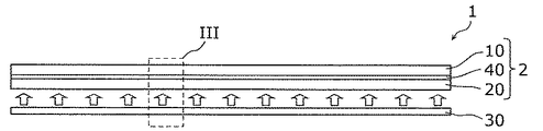
まず、実施の形態に係る液晶表示装置1の概略構成について、図1及び図2を用いて説明する。図1は、実施の形態に係る液晶表示装置1の概略構成を模式的に示す図である。図2は、同液晶表示装置1の断面構成を模式的に示す図である。なお、図1及び図2に示される矢印は、バックライト30から出射する光を模式的に示している。
(Embodiment)
[Schematic configuration of liquid crystal display]
First, a schematic configuration of the liquid
図1及び図2に示すように、本実施の形態に係る液晶表示装置1は、静止画像又は動画像の画像(映像)を表示するための画像表示装置の一例であって、液晶モジュール2と、バックライト30とを備える。液晶モジュール2は、第1の液晶パネル10と、第2の液晶パネル20と、拡散シート40とを備える。つまり、液晶表示装置1全体としては、第1の液晶パネル10と、第2の液晶パネル20と、バックライト30と、拡散シート40とを備える。液晶表示装置1において、第1の液晶パネル10、拡散シート40、第2の液晶パネル20及びバックライト30は、第1の液晶パネル10からバックライト30に向かって、この順で配置されている。
As shown in FIGS. 1 and 2, a liquid
第1の液晶パネル10は、メインパネルであって、ユーザが視認する画像を表示する。本実施の形態において、第1の液晶パネル10は、カラー画像を表示する。第1の液晶パネル10は、第2の液晶パネル20の前面側に配置される。
The 1st
第2の液晶パネル20は、第1の液晶パネル10の背面側に配置されるサブパネルである。第2の液晶パネル20は、第1の液晶パネル10に表示されるカラー画像に対応した画像のモノクロ画像を、そのカラー画像に同期させて表示する。第2の液晶パネル20は、バックライト30及び第1の液晶パネル10の間に配置される。
The second
第1の液晶パネル10及び第2の液晶パネル20は、画像が表示される画像表示領域として、マトリクス状に配列された複数の画素を有する。第1の液晶パネル10の画素数と第2の液晶パネル20の画素数とは同じでなくてもよいが、メインパネルである第1の液晶パネル10の方が画素数が多いとよい。また、第1の液晶パネル10及び第2の液晶パネル20の駆動方式は、例えばIPS(In Plane Switching)方式であるが、これに限るものではなく、VA(Vertical Alignment)方式又はTN(Twisted Nematic)方式等であってもよい。
The first
バックライト30は、第1の液晶パネル10及び第2の液晶パネル20に向けて光を照射する。バックライト30は、均一な散乱光(拡散光)を照射する面光源である。バックライト30は、第2の液晶パネル20の背面側に配置される。バックライト30は、例えば、LED(Light Emitting Diode)を光源とするLEDバックライトであるが、これに限るものではない。また、本実施の形態において、バックライト30は、直下型であるが、エッジ型であってもよい。なお、バックライト30は、光源からの光を拡散させるために拡散板(拡散シート)等の光学部材を有する。
The
拡散シート40は、第1の液晶パネル10及び第2の液晶パネル20の間に配置された光学部材である。拡散シート40は、入射した光を拡散(散乱)させる光拡散層として機能する。したがって、第2の液晶パネル20から拡散シート40に入射した光は、拡散シート40で拡散されて拡散シート40を透過し、第1の液晶パネル10に入射する。拡散シート40は、例えば、樹脂材料に反射性微粒子が分散された樹脂シートであるが、これに限るものではなく、微小凹凸構造等によって光を拡散させるものであってもよい。
The
なお、図示しないが、第1の液晶パネル10、拡散シート40及び第2の液晶パネル20は互いに貼り合わされて、バックライト30とともに、金属製又は樹脂製の保持部材(筐体、フレーム又はシャーシ)に保持される。また、第1の液晶パネル10及び第2の液晶パネル20には、フレキシブル基板を介してドライバ基板が接続されている。
Although not shown, the first
このように、本実施の形態に係る液晶表示装置1では、第1の液晶パネル10及び第2の液晶パネル20の2つの液晶パネルを重ね合わせて画像を表示しているので、黒を引き締めることができる。これにより、高コントラスト比の画像を表示することができる。また、液晶表示装置1は、例えばHDR(High Dynamic Range)対応テレビであり、バックライト30として、ローカルディミング対応の直下型LEDバックライトを用いている。したがって、高コントラスト比かつ高画質のカラー画像を表示することができる。
As described above, in the liquid
[液晶表示装置の詳細構成]
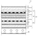
次に、図3を用いて、液晶表示装置1の詳細な構成を説明する。図3は、実施の形態に係る液晶表示装置1の拡大断面図である。図3は、図2の破線で囲まれる領域IIIを拡大して示している。
[Detailed configuration of liquid crystal display]
Next, a detailed configuration of the liquid
まず、第1の液晶パネル10について説明する。図3に示すように、第1の液晶パネル10は、一対の第1の透明基板11と、第1の液晶層12と、一対の第1の偏光板13とを有する。
First, the first
一対の第1の透明基板11の各々は、例えばガラス基板であり、互いに対面するように配置されている。本実施の形態において、一対の第1の透明基板11のうち第2の液晶パネル20側の位置する第1の透明基板11がTFT(Thin Film Transistor)等を形成するためのTFT基板である第1のTFT基板11aであり、一対の第1の透明基板11のうち第2の液晶パネル20側とは反対側に位置する第1の透明基板11が第1の対向基板11bである。
Each of the pair of first
第1のTFT基板11aの第1の液晶層12側の面には、TFT又は配線等が設けられたTFT層14(第1のTFT層)が形成されている。また、TFT層14の平坦化層上には、第1の液晶層12に電圧を印加するための画素電極が形成されている。本実施の形態では第1の液晶パネル10がIPS方式により駆動されるので、第1のTFT基板11aには、画素電極だけではなく、対向電極も形成されている。TFT、画素電極及び対向電極等は、画素ごとに形成されている。また、画素電極及び対向電極を覆うように配向膜が形成されている。
A TFT layer 14 (first TFT layer) provided with TFTs or wirings is formed on the surface of the
第1の対向基板11bは、カラーフィルタ15bが形成されたカラーフィルタ基板(CF基板)であり、第1の対向基板11bの第1の液晶層12側の面には、第1のブラックマトリクス15a及びカラーフィルタ15bを有する画素形成層15(第1の画素形成層)が形成されている。
The
画素形成層15は、一対の第1の透明基板11の間に配置されている。つまり、第1のブラックマトリクス15a及びカラーフィルタ15bは、一対の第1の透明基板11の間に配置されている。
The
第1のブラックマトリクス15aには、画素を構成するマトリクス状の複数の第1の開口部15a1が形成されている。つまり、複数の第1の開口部15a1の各々は、複数の画素の各々に対応している。第1のブラックマトリクス15aは、例えば、各第1の開口部15a1の平面視形状が矩形状となるように、格子状に形成されている。
In the first
カラーフィルタ15bは、第1のブラックマトリクス15aの第1の開口部15a1の内部に形成されている。カラーフィルタ15bは、例えば、赤色用のカラーフィルタ、緑色用のカラーフィルタ、及び、青色用のカラーフィルタによって構成されている。各色のカラーフィルタは、各画素に対応している。
The
なお、画素形成層15を覆うようにオーバーコート層が形成されている。さらに、オーバーコート層の表面(第1の液晶層12側の面)には配向膜が形成されている。
An overcoat layer is formed so as to cover the
第1の液晶層12は、一対の第1の透明基板11の間に封止されている。具体的には、第1のTFT基板11aに形成された配向膜と第1の対向基板11bに形成された配向膜との間に封止されている。第1の液晶層12の液晶材料は、駆動方式に応じて適宜選択することができる。第1の液晶層12の厚さは、例えば、2.5μm〜6μmであるが、これに限るものではない。一例として、第1の液晶層12の厚さは、3.4μmである。
The first
一対の第1の偏光板13は、樹脂材料からなるシート状の偏光フィルムであり、一対の第1の透明基板11を挟むように配置されている。具体的には、一対の第1の偏光板13のうちの一方が第1のTFT基板11aの外面(第1の液晶層12側とは反対側の面)に貼り合わされており、一対の第1の偏光板13のうちの他方が第1の対向基板11bの外面(第1の液晶層12側とは反対側の面)に貼り合わされている。また、一対の第1の偏光板13は、偏光方向が互いに直交するように配置されている。つまり、一対の第1の偏光板13は、クロスニコルで配置されている。
The pair of first
本実施の形態において、一対の第1の偏光板13のうち拡散シート40から遠い方の第1の偏光板13(つまり、第1の対向基板11bに貼り合わされた方の第1の偏光板13)の一方側の面には、位相差板(位相差フィルム)が貼り合わされている。なお、位相差板は、第1の偏光板13と第1の対向基板11bとの間以外の場所に設けられていてもよい。例えば、第2の液晶パネル20の一対の第2の偏光板23のうち拡散シート40から遠い方の第2の偏光板23(つまり、第2の対向基板21bに貼り合わされた方の第2の偏光板23)の一方側の面に、位相差板が貼り合わされていてもよい。また、第1の偏光板13及び第2の偏光板23の両方に貼り合わされていてもよい。
In the present embodiment, of the pair of first
一対の第1の偏光板13の各々の厚さは、例えば、0.05mm〜0.5mmであるが、これに限るものではない。一例として、第1の偏光板13の厚さは、いずれも0.2mmである。また、本実施の形態では、第1の対向基板11bに貼り合わされた方の第1の偏光板13(厚さ0.2mm)には、厚さ0.1mmの位相差板が貼り合わされている。
The thickness of each of the pair of first
次に、第2の液晶パネル20について説明する。第2の液晶パネル20は、一対の第2の透明基板21と、第2の液晶層22と、一対の第2の偏光板23とを有する。
Next, the second
一対の第2の透明基板21の各々は、例えばガラス基板であり、互いに対面するように配置されている。本実施の形態において、一対の第2の透明基板21のうちバックライト30側に位置する第2の透明基板21が第2のTFT基板21aであり、一対の第2の透明基板21のうち第1の液晶パネル10側に位置する第2の透明基板21が第2の対向基板21bである。
Each of the pair of second
第2のTFT基板21aは、第1の液晶パネル10の第1のTFT基板11aと同様の構成である。したがって、第2のTFT基板21aの第2の液晶層22側の面にはTFT層24(第2のTFT層)が形成されており、TFT層24の平坦化層上には画素ごとに画素電極及び対向電極が形成されている。また、画素電極及び対向電極を覆うように配向膜が形成されている。
The
第2の対向基板21bの第2の液晶層22側の面には、第2のブラックマトリクス25aを有する画素形成層25(第2の画素形成層)が形成されている。画素形成層25は、一対の第2の透明基板21の間に配置されている。つまり、第2のブラックマトリクス25aは、一対の第2の透明基板21の間に配置されている。
A pixel formation layer 25 (second pixel formation layer) having a second
第2のブラックマトリクス25aには、画素を構成するマトリクス状の複数の第2の開口部25a1が形成されている。つまり、複数の第2の開口部25a1の各々は、複数の画素の各々に対応している。第2のブラックマトリクス25aは、例えば、各第2の開口部25a1の平面視形状が矩形状となるように、格子状に形成されている。
In the second
なお、画素形成層25を覆うようにオーバーコート層が形成されている。さらに、オーバーコート層の表面(第2の液晶層22側の面)には配向膜が形成されている。また、本実施の形態において、第2の液晶パネル20はモノクロ画像を表示するので、第2の対向基板21bには、カラーフィルタが形成されていない。したがって、複数の第2の開口部25a1の内部には、オーバーコート層が形成されている。
An overcoat layer is formed so as to cover the
第2の液晶層22は、一対の第2の透明基板21の間に封止されている。具体的には、第2のTFT基板21aに形成された配向膜と第2の対向基板21bに形成された配向膜との間に封止されている。第2の液晶層22の液晶材料は、駆動方式に応じて適宜選択することができる。第2の液晶層22の厚さは、例えば、2.5μm〜6μmであるが、これに限るものではない。一例として、第2の液晶層22の厚さは、3.4μmである。
The second
一対の第2の偏光板23は、樹脂材料からなるシート状の偏光フィルムであり、一対の第2の透明基板21を挟むように配置されている。具体的には、一対の第2の偏光板23のうちの一方が第2のTFT基板21aの外面(第2の液晶層22側とは反対側の面)に貼り合わされており、一対の第2の偏光板23のうちの他方が第2の対向基板21bの外面(第2の液晶層22側とは反対側の面)に貼り合わされている。また、一対の第2の偏光板23は、偏光方向が互いに直交するように配置されている。つまり、一対の第2の偏光板23は、クロスニコルで配置されている。
The pair of second
なお、一対の第2の偏光板23の各々の厚さは、例えば、0.05mm〜0.5mmであるが、これに限るものではない。本実施の形態において、第2の偏光板23の厚さは、いずれも0.2mmである。
In addition, although each thickness of a pair of 2nd
拡散シート40は、上記のように、第1の液晶パネル10と第2の液晶パネル20との間に配置されている。具体的には、拡散シート40は、第1の液晶パネル10の第1の透明基板11と第2の液晶パネル20の第2の透明基板21との間に配置されている。より具体的には、拡散シート40は、第1の液晶パネル10の第1のTFT基板11aと第2の液晶パネル20の第2の対向基板21bとの間に配置されている。
The
拡散シート40は、第1の液晶パネル10(第1の透明基板11)及び第2の液晶パネル20(第2の透明基板21)に貼り合わされている。この場合、拡散シート40は、光学粘着シート(OCA:Optically Clear Adhesive)等の接着剤によって第1の液晶パネル10及び第2の液晶パネル20に接着されていてもよいし、拡散シート40そのものが接着性を有する場合は、拡散シート40が第1の液晶パネル10及び第2の液晶パネル20の各々に直接接着されていてもよい。
The
なお、拡散シート40の厚さは、例えば、0.15mm〜0.6mmであるが、これに限るものではない。一例として、拡散シート40の厚さは、0.3mmである。
In addition, although the thickness of the
そして、このように構成される液晶表示装置1では、一対の第1の透明基板11のうち拡散シート40に近い方の第1の透明基板11(本実施の形態では、第1のTFT基板11a)の厚さが、一対の第2の透明基板21のうち拡散シート40に近い方の第2の透明基板21(本実施の形態では、第2の対向基板21b)の厚さよりも薄くなっている。つまり、重ね合わせた第1の液晶パネル10及び第2の液晶パネル20における一対の第1の透明基板11及び一対の第2の透明基板21の4つの透明基板のうち、拡散シート40を挟む内側の2つの透明基板について、第1の液晶パネル10の透明基板である第1の透明基板11の厚さの方が、第2の液晶パネル20の透明基板である第2の透明基板21の厚さよりも相対的に薄くなっている。
In the liquid
この場合、図3に示すように、一対の第1の透明基板11において、第1のTFT基板11aの厚さをt11aとし、第1の対向基板11bの厚さをt11bとし、また、一対の第2の透明基板21において、第2のTFT基板21aの厚さをt21aとし、第2の対向基板21bの厚さをt21bとすると、少なくともt11a<t21bの関係を満たしている。一例として、t11a=0.5mm、t11b=0.7mm、t21a=0.7mm、t21b=0.7mmである。
In this case, as shown in FIG. 3, the first
さらに、一対の第1の透明基板11のうち拡散シート40に近い方の第1の透明基板11(本実施の形態では、第1のTFT基板11a)の厚さは、一対の第2の透明基板21のうち拡散シート40に近い方の第2の透明基板21(本実施の形態では、第2の対向基板21b)の厚さの略1/2以下であるとよい。この場合、一例として、t11a=0.3mm、t11b=0.7mm、t21a=0.7mm、t21b=0.7mmである。
Furthermore, the thickness of the first transparent substrate 11 (in this embodiment, the
また、一対の第1の透明基板11のうち拡散シート40から遠い方の第1の透明基板11(本実施の形態では、第1の対向基板11b)と、一対の第2の透明基板21のうち拡散シート40に近い方の第2の透明基板21(本実施の形態では、第2の対向基板21b)と、一対の第2の透明基板21のうち拡散シート40から遠い方の第2の透明基板21(本実施の形態では、第2のTFT基板21a)とは、厚さが略同一となっている。つまり、t11b=t21a=t21bである。
Further, of the pair of first
なお、t11a、t11b、t21a、t21bの値は、0.3mm、0.5mm、0.7mmの中から任意に選択することができる。また、t11a、t11b、t21a、t21bの値は、これらの数値に限定されるものではなく、第1の透明基板11及び第2の透明基板21がガラス基板である場合、0.2mm以上であれば、任意の値(例えば、0.4mm、1.0mm等)を適宜変更することができる。なお、第1の透明基板11及び第2の透明基板21がガラス基板である場合、厚さが0.2mm未満になると、ガラス基板が割れやすくなり、製造時等のハンドリングが難しくなる。
Note that the values of t 11a , t 11b , t 21a , and t 21b can be arbitrarily selected from 0.3 mm, 0.5 mm, and 0.7 mm. In addition, the values of t 11a , t 11b , t 21a , and t 21b are not limited to these numerical values, and when the first
また、一対の第1の透明基板11及び一対の第2の透明基板21の厚さについては、一定の厚さの透明基板を薄く加工することで所定の厚さに調整してもよいし、薄くする加工を施すことなく基板成形時当初からの厚さであってもよい。なお、透明基板としてガラス基板を用いて薄く加工する場合、ガラス基板をフッ酸に浸漬してエッチングすることでガラス基板を薄くすることができる。具体的には、厚さ0.7mmのガラス基板をフッ酸でエッチングすることで、0.5mm、0.3mm等の厚さにまで薄くすることができる。
Further, the thickness of the pair of first
[液晶表示装置の作用等]
次に、本実施の形態に係る液晶表示装置1の作用について、本開示の技術を得るに至った経緯も含めて、図4〜図6を用いて説明する。図4は、拡散シート40によるモアレの抑制効果を説明するための図である。図5は、比較例に係る液晶表示装置100の拡大断面図である。図6は、2つの液晶パネルを重ねることで生じる視差の影響を説明するための図である。
[Operation of liquid crystal display device]
Next, the operation of the liquid
図4の(a)に示すように、カラー画像を表示する第1の液晶パネル110とモノクロ画像を表示する第2の液晶パネル20とを重ね合わせると、モアレが発生する。つまり、第2の液晶パネル20の画素を形成する格子状の第2のブラックマトリクス25aの上に、第1の液晶パネル110の画素を形成する格子状の第1のブラックマトリクス15aが存在すると、画素ピッチに依存する明暗模様(モアレ縞)が発生する。これにより、第1の液晶パネル110に表示される画像の品位が低下する。
As shown in FIG. 4A, moire occurs when the first
そこで、図4の(b)に示すように、第1の液晶パネル110と第2の液晶パネル20との間に拡散シート40を挿入することが考えられる。これにより、第2の液晶パネル20から出射する光を拡散シート40によって拡散(散乱)させることができる。すなわち、拡散シート40と第2のブラックマトリクス25aとの間において光を空間的に混ぜることができる。この結果、モアレの発生を抑制することができる。つまり、モアレによる画像品位の低下を抑制することができる。
Therefore, as shown in FIG. 4B, it is conceivable to insert a
具体的には、図5に示すような構造の液晶表示装置100が考えられる。図5に示すように、比較例に係る液晶表示装置100は、第1の液晶パネル110と、第2の液晶パネル20と、バックライト30と、拡散シート40とを備える。
Specifically, a liquid
第1の液晶パネル110は、一対の第1の透明基板111と、第1の液晶層12と、一対の第1の偏光板13とを有する。一対の第1の透明基板111は、第1のTFT基板111aと第1の対向基板111bとによって構成されている。第1のTFT基板111aには、TFT層14が形成され、第1の対向基板111bには、第1のブラックマトリクス15a及びカラーフィルタ15bを有する画素形成層15が形成されている。
The first
なお、図5における、第2の液晶パネル20、バックライト30及び拡散シート40は、図3における、第2の液晶パネル20、バックライト30及び拡散シート40と同様の構成である。
In addition, the 2nd
図5に示される液晶表示装置100において、4枚のガラス基板は全て同じ厚さである。つまり、第1のTFT基板111a、第1の対向基板111b、第2のTFT基板21a、及び、第2の対向基板21bの厚さは、同じであり、例えば0.7mmである。したがって、図5に示される液晶表示装置100と図3に示される液晶表示装置1とでは、第1のTFT基板111a(図5)の厚さと第1のTFT基板11a(図3)の厚さのみが異なっている。
In the liquid
このように、図5に示される液晶表示装置100によれば、第1の液晶パネル110と第2の液晶パネル20との間に拡散シート40が設けられているので、拡散シート40を設けない場合と比べて、モアレによる画像品位の低下を抑制することができる。
As described above, according to the liquid
しかしながら、複数の液晶パネルを重ね合わせると、視差が発生して画像品位が低下するという課題がある。例えば、視差の影響によって、画像を斜めから見た場合に輝度が低下したり、画像が二重に見えたりする。 However, when a plurality of liquid crystal panels are overlapped, there is a problem that parallax is generated and image quality is lowered. For example, due to the influence of parallax, when the image is viewed obliquely, the luminance decreases or the image looks double.
ここで、図6を用いて、第1の液晶パネル110及び第2の液晶パネル20の2つの液晶パネルを重ねることで生じる視差の影響を説明する。
Here, the influence of parallax generated by overlapping two liquid crystal panels of the first
図6の(a)に示すように、第1の液晶パネル110と第2の液晶パネル20との間隔を広くすると、小さな角度θで視差が生じるが、図6の(b)に示すように、第1の液晶パネル110と第2の液晶パネル20との間隔を狭くすると、比較的に大きな角度θまで視差が生じない。
As shown in FIG. 6A, when the interval between the first
このような視差は、第1の液晶パネル110の第1のブラックマトリクス15a及び第2の液晶パネル20の第2のブラックマトリクス25aが影響していると考えられる。具体的には、第1のブラックマトリクス15aと第2のブラックマトリクス25aとの距離Lが視差に影響していると考えられる。
It is considered that such parallax is influenced by the first
したがって、図6の(a)に示すように、第1のブラックマトリクス15aと第2のブラックマトリクス25aとの距離Lが比較的に大きい場合には、小さな角度θで視差が生じるが、図6の(b)に示すように、第1のブラックマトリクス15aと第2のブラックマトリクス25aとの距離Lが小さい場合には、比較的に大きな角度θまで視差が生じない。
Therefore, as shown in FIG. 6A, when the distance L between the first
このように、第1の液晶パネル110と第2の液晶パネル20との間隔を狭くして第1のブラックマトリクス15aと第2のブラックマトリクス25aとの距離Lを小さくすることで、視差による画像品位の低下を抑制することができる。
In this way, by reducing the distance L between the first
しかしながら、第1の液晶パネル110(第1のブラックマトリクス15a)と第2の液晶パネル20(第2のブラックマトリクス25a)の間隔を単に狭くしてしまうと、拡散シート40の挿入によるモアレの抑制効果が低下する。
However, if the distance between the first liquid crystal panel 110 (first
例えば、4つのガラス基板(一対の第1の透明基板111、一対の第2の透明基板21)を全て薄くしたり、第1のブラックマトリクス15a及び第2のブラックマトリクス25aの間にある2つのガラス基板(第1のTFT基板111a、第2の対向基板21b)を薄くしたりして、第1のブラックマトリクス15a及び第2のブラックマトリクス25aの間隔を狭くすると、拡散シート40の挿入によるモアレの抑制効果が低下する。
For example, all four glass substrates (a pair of first
本開示の技術は、このような知見に基づいてなされたものであり、本願発明者らが鋭意検討した結果、第1のTFT基板111a及び第2の対向基板21bのうち第1のTFT基板111aの厚さを薄くすることで、モアレの抑制効果を犠牲にすることなく、視差による画像品位の低下を抑制できることを見出した。
The technology of the present disclosure has been made based on such knowledge, and as a result of intensive studies by the present inventors, the
特に、本願発明者らは、メインパネルである第1の液晶パネル10の第1のブラックマトリクス15aとサブパネルである第2の液晶パネル20の第2のブラックマトリクス25aとの間に着目し、図3に示すように、第1のブラックマトリクス15aと第2のブラックマトリクス25aとの間に存在する2つの透明基板のうち、第1の液晶パネル10の透明基板の厚さを第2の液晶パネル20の透明基板の厚さよりも相対的に薄くすることを考えた。
In particular, the inventors of the present application pay attention to the area between the first
すなわち、一対の第1の透明基板11のうち拡散シート40に近い方の第1の透明基板11(第1のTFT基板11a)の厚さを、一対の第2の透明基板21のうち拡散シート40に近い方の第2の透明基板21(第2の対向基板21b)の厚さよりも薄くしている。
That is, the thickness of the first transparent substrate 11 (
このように構成することで、第1のTFT基板11a及び第2の対向基板21bの両方を薄くする場合と比べて、モアレの抑制効果が低下してしまうことを抑制することができる。つまり、拡散シート40の挿入によるモアレの抑制効果を維持することができる。
By configuring in this way, it is possible to suppress a decrease in the moire suppressing effect as compared with the case where both the
しかも、一対の第1の透明基板11のうち拡散シート40に近い方の第1の透明基板11(第1のTFT基板11a)の厚さを、一対の第2の透明基板21のうち拡散シート40に近い方の第2の透明基板21(第2の対向基板21b)の厚さよりも薄くすることで、第1のブラックマトリクス15aと第2のブラックマトリクス25aとの距離を小さくすることができる。これにより、視差による画像品位の低下を抑制することができる。
Moreover, the thickness of the first transparent substrate 11 (
また、本実施の形態における液晶表示装置1では、拡散シート40が、第1のブラックマトリクス15a及び第2のブラックマトリクス25aのうち第1のブラックマトリクス15a寄りに配置されている。つまり、拡散シート40が、第1のブラックマトリクス15a及び第2のブラックマトリクス25aの間の中心と第1のブラックマトリクス15aとの間に位置しており、第1のブラックマトリクス15aと第2のブラックマトリクス25aとの間の距離の半分よりも第1のブラックマトリクス15a側に配置されている。
Further, in the liquid
これにより、モアレをより効果的に抑制することができる。この点について、図7を用いて説明する。図7は、実施の形態に係る液晶表示装置1のモアレの抑制効果を説明するための図である。
Thereby, moire can be more effectively suppressed. This point will be described with reference to FIG. FIG. 7 is a diagram for explaining the moire suppression effect of the liquid
図7の(a)に示すように、拡散シート40が、第1のブラックマトリクス15a及び第2のブラックマトリクス25aのうち第2のブラックマトリクス25a寄りに配置されていると、拡散シート40と第2のブラックマトリクス25aとの間隔が狭くなるので、空間的に光を混ぜる効果が小さくなってしまう。このため、モアレの抑制効果が小さくなり、モアレが残る場合がある。すなわち、拡散シート40と第2のブラックマトリクス25aとの間隔が狭い場合、第2のブラックマトリクス25aの開口部25a1を透過した光が十分に拡がる前に拡散シート40に入射してしまうため、拡散シート40に、光が相対的に多く入射する領域と、光が相対的に少なく入射する領域と、が繰り返し生じてしまい、拡散シート40に明暗のパターンが残ってしまう。このため、第1の液晶パネル10の第1のブラックマトリクス15aを介して拡散シート40を観察した際に、拡散シート40の明暗のパターンに起因するモアレが認識されてしまいやすい。
As shown in FIG. 7A, when the
これに対して、図7の(b)に示すように、拡散シート40が、第1のブラックマトリクス15a及び第2のブラックマトリクス25aのうち第1のブラックマトリクス15a寄りに配置されていると、拡散シート40と第2のブラックマトリクス25aとの間隔が広くなるので、空間的に光を混ぜる効果が大きくなる。これにより、モアレの抑制効果を大きくすることができるので、モアレを効果的に抑制することができる。すなわち、拡散シート40と第2のブラックマトリクス25aとの間隔が広い場合、第2のブラックマトリクス25aの開口部25a1を透過した光が十分に拡がった後に拡散シート40に入射するため、拡散シート40で第2のブラックマトリクス25aの開口部25a1を透過した光が十分に空間的に混ざり合う。このため、拡散シート40に明暗のパターンがほとんど生じず、モアレを効果的に抑制することができる。
On the other hand, as shown in FIG. 7B, when the
[まとめ]
以上説明したように、本実施の形態における液晶モジュール2は、バックライト30に対向して配置されており、一対の第1の透明基板11を有する第1の液晶パネル10と、バックライト30及び第1の液晶パネル10の間に配置され、一対の第2の透明基板21を有する第2の液晶パネル20と、第1の液晶パネル10及び第2の液晶パネル20の間に配置された拡散シート40とを備えている。
[Summary]
As described above, the
そして、一対の第1の透明基板11のうち拡散シート40に近い方の第1の透明基板11の厚さが、一対の第2の透明基板21のうち拡散シート40に近い方の第2の透明基板21の厚さよりも薄くなっている。具体的には、第1の液晶パネル10の第1のTFT基板11aの厚さが、第2の液晶パネル20の第2の対向基板21bの厚さよりも薄くなっている。
The thickness of the first
これにより、モアレの抑制効果を維持しつつ、視差による画像品位の低下を抑制することができる。つまり、モアレの抑制効果を犠牲にすることなく、視差による画像品位の低下を抑制できる。このように、本実施の形態における液晶モジュール2によれば、モアレによる画像品位の低下の抑制と視差による画像品位の低下の抑制との両立を図ることができる。
As a result, it is possible to suppress a reduction in image quality due to parallax while maintaining the moire suppression effect. That is, it is possible to suppress a reduction in image quality due to parallax without sacrificing the moire suppressing effect. As described above, according to the
しかも、第1のTFT基板11a及び第2の対向基板21bのうち第2の対向基板21bが第1のTFT基板11aに対して相対的に厚くなるので、第2の液晶パネル20によって機械的強度が確保することができる。これにより、第1のTFT基板11aを薄くしたとしても、液晶モジュール2の機械的強度を維持することができる。また、第1のTFT基板11aのみを薄く加工すればよく、第2の対向基板21bを薄く加工する必要がないので、製造コストが高くなることを抑制できる。さらに、第2の対向基板21bの厚さを相対的に厚くしておくことで、バックライト30からの熱に対する熱対策できるという効果も得られる。
Moreover, since the
また、本実施の形態における液晶モジュール2において、一対の第1の透明基板11のうち拡散シート40に近い方の第1の透明基板11(第1のTFT基板11a)の厚さは、一対の第2の透明基板21のうち拡散シート40に近い方の第2の透明基板21(第2の対向基板21b)の厚さの5/7以下であるとよい。
In the
これにより、一対の第1の透明基板11のうち拡散シート40に近い方の第1の透明基板11(第1のTFT基板11a)の厚さが、一対の第2の透明基板21のうち拡散シート40に近い方の第2の透明基板21(第2の対向基板21b)の厚さの5/7を超える場合と比べて、視差による画像品位の低下を一層効果的に抑制することができる。このような傾向をより強化する観点から、一対の第1の透明基板11のうち拡散シート40に近い方の第1の透明基板11(第1のTFT基板11a)の厚さは、一対の第2の透明基板21のうち拡散シート40に近い方の第2の透明基板21(第2の対向基板21b)の厚さの略1/2以下であってもよい。
Accordingly, the thickness of the first transparent substrate 11 (
また、本実施の形態における液晶モジュール2において、拡散シート40は、第1のブラックマトリクス15a及び第2のブラックマトリクス25aのうち第1のブラックマトリクス15a寄りに配置されている。
Further, in the
これにより、より効果的にモアレを抑制することができる。したがって、モアレを発生させることなく、視差による画像品位の低下を抑制することができるので、高品位の画像表示が可能となる。 Thereby, moire can be more effectively suppressed. Accordingly, it is possible to suppress a reduction in image quality due to parallax without generating moire, and thus it is possible to display a high-quality image.
また、本実施の形態における液晶モジュール2において、一対の第1の透明基板11のうち拡散シート40から遠い方の第1の透明基板11(第1の対向基板11b)と、一対の第2の透明基板21のうち拡散シート40に近い方の第2の透明基板21(第2の対向基板21b)と、一対の第2の透明基板21のうち拡散シート40から遠い方の第2の透明基板21(第2のTFT基板21a)とは、厚さが略同一である。
In the
これにより、液晶モジュール2における4つの透明基板(第1のTFT基板11a、第1の対向基板11b、第2のTFT基板21a、第2の対向基板21b)のうち、1つの透明基板(第1のTFT基板11a)のみの厚さが薄くなる。したがって、モアレを抑制でき、かつ、視差の影響のない画像を表示できる液晶モジュール2を低コストで製造することができる。
Thereby, one transparent substrate (
また、本実施の形態における液晶モジュール2において、一対の第1の偏光板13のうち拡散シート40から遠い方の第1の偏光板13の一方側の面には、位相差板が貼り合わされている。
Further, in the
このように、位相差板を設けることで、一対の第1の偏光板13による偏光成分に位相差(光路差)をつけて入射偏光の状態を変えることができる。これにより、第2の液晶パネル20から第1の液晶パネル10に入射する光のうち斜め方向に進む光の透過を抑制できるので、ハローの発生を抑制することができる。特に、拡散シート40から遠い方の第1の偏光板13と第1の対向基板11bとの間に位相差板を挿入することで、より斜め方向の視差を低減することができる。
As described above, by providing the retardation plate, it is possible to change the state of the incident polarized light by adding a phase difference (optical path difference) to the polarization component by the pair of first
また、本実施の形態における液晶モジュール2において、第1の液晶パネル10は、カラー画像を表示し、第2の液晶パネル20は、モノクロ画像を表示する。
Further, in the
これにより、モノクロ画像の重ね合わせによってカラー画像の黒を引き締めることができるので、高コントラスト比のカラー画像を表示することができる。 As a result, the black color image can be tightened by superimposing the monochrome images, so that a color image with a high contrast ratio can be displayed.
また、本実施の形態における液晶表示装置1は、液晶モジュール2と、液晶モジュール2に対向して配置されたバックライト30とを備える。
In addition, the liquid
これにより、モアレの抑制効果を維持しつつ、視差による画像品位の低下を抑制することができる液晶表示装置を実現できる。 Accordingly, it is possible to realize a liquid crystal display device that can suppress a reduction in image quality due to parallax while maintaining a moire suppressing effect.
(変形例1)
図8は、変形例1に係る液晶表示装置1Aの拡大断面図である。本変形例における液晶表示装置1Aは、上記実施の形態と同様に、液晶モジュール2Aとバックライト30とを備える。
(Modification 1)
FIG. 8 is an enlarged cross-sectional view of a liquid
本変形例に係る液晶表示装置1Aは、上記実施の形態に係る液晶表示装置1において、拡散シート40を複数枚で構成したものである。
A liquid
具体的には、図8に示すように、本変形例に係る液晶表示装置1Aでは、拡散シート40Aが第1の拡散シート41及び第2の拡散シート42の2層構造を有する。なお、それ以外の構成は、上記実施の形態に係る液晶表示装置1と同じである。
Specifically, as shown in FIG. 8, in the liquid
本変形例において、第1の拡散シート41は、第1の液晶パネル10に貼り合わされている。具体的には、第1の拡散シート41は、第1の液晶パネル10の第1の透明基板11(第1のTFT基板11a)に貼り合わされている。
In the present modification, the
一方、第2の拡散シート42は、第2の液晶パネル20に貼り合わされている。具体的には、第2の拡散シート42は、第2の液晶パネル20の第2の透明基板21(第2の対向基板21b)に貼り合わされている。
On the other hand, the
拡散シート40Aの第1の液晶パネル10及び第2の液晶パネル20への貼り合わせは、次のようにして行うことができる。例えば、第1の拡散シート41を第1の液晶パネル10に予め貼り合わせておくとともに、第2の拡散シート42を第2の液晶パネル20に予め貼り合わせておく。その後、第1の拡散シート41と第2の拡散シート42とを、光学粘着シート等の接着剤によって貼り合わせることで、第1の液晶パネル10と第2の液晶パネル20の間に拡散シート40Aが挿入された液晶表示装置1Aを製造することができる。
The bonding of the
このように、拡散シート40Aを複数に分けて第1の液晶パネル10及び第2の液晶パネルに予め貼り付けることで、第1の液晶パネル10と第2の液晶パネル20との間に拡散シート40Aを有する液晶表示装置1Aを容易に製造することができる。
As described above, the
なお、先に第1の拡散シート41及び第2の拡散シート42を第1の液晶パネル10及び第2の液晶パネル20に貼り合わせるのではなく、第1の拡散シート41と第2の拡散シート42とを先に貼り合わせて拡散シート40Aを作製してから、実施の形態1と同様にして、拡散シート40Aを第1の液晶パネル10及び第2の液晶パネル20に貼り合わせてもよい。
Note that the
また、本変形例では、第1の液晶パネル10側に位置する第1の拡散シート41の厚さを、第2の液晶パネル20側に位置する第2の拡散シート42の厚さよりも薄くしている。
Further, in this modification, the thickness of the
これにより、より効果的にモアレを抑制しつつ、視差による画像品位の低下を抑制することができる。この点について、以下に説明する。 As a result, it is possible to suppress a decrease in image quality due to parallax while more effectively suppressing moire. This point will be described below.
例えば、第1の拡散シート41及び第2の拡散シート42の厚さが同じである場合に、視差による画像品位の低下のさらに抑制するために拡散シート40Aの厚さを薄くする際、仮に第1の拡散シート41及び第2の拡散シート42のうち第2の拡散シート42の方を薄くすると、第1のブラックマトリクス15aと第2のブラックマトリクス25aとの間において、拡散シート40Aは相対的に第2のブラックマトリクス25a寄りに位置することになる。これに対して、本変形例にように、第1の拡散シート41及び第2の拡散シート42のうち第1の拡散シート41の方を薄くすると、第1のブラックマトリクス15aと第2のブラックマトリクス25aとの間において、拡散シート40Aは相対的に第1のブラックマトリクス15a寄りに位置することになる。これにより、図7で説明したように、空間的に光を混ぜる効果を大きくすることが可能となるので、モアレを効果的に抑制することができる。したがって、より効果的にモアレを抑制しつつ、視差による画像品位の低下を抑制することができる。
For example, when the thickness of the
また、本変形例において、第1の拡散シート41の拡散度は、第2の拡散シート42の拡散度よりも大きい方がよい。これにより、第1の液晶パネル10に近い方の第1の拡散シート41のヘイズ値が、第2の液晶パネル20に近い方の第2の拡散シート42のヘイズ値よりも大きくなる。
In the present modification, the diffusion degree of the
これにより、モアレの抑制効果を大きくすることができる。したがって、より効果的にモアレを抑制しつつ、視差による画像品位の低下を抑制することができる。 Thereby, the suppression effect of a moire can be enlarged. Therefore, it is possible to suppress a decrease in image quality due to parallax while more effectively suppressing moire.
第1の拡散シート41及び第2の拡散シート42の拡散度は、第1の拡散シート41及び第2の拡散シート42に含まれる反射性微粒子の濃度(密度)を変更したり、第1の拡散シート41及び第2の拡散シート42の厚さを変更したりすることで調整できる。後者の場合、第1の拡散シート41の厚さを厚くすること拡散度を大きくできるが、上記のように、第1の拡散シート41の厚さは薄い方がよいので、反射性微粒子の濃度を大きくすることで、第1の拡散シート41の拡散度を大きくする方がよい。
The degree of diffusion of the
なお、本変形例において、拡散シート40Aは、2層としたが、3層以上であってもよい。また、本変形例では、第1の拡散シート41と第2の拡散シート42との間に接着層を形成したが、第1の拡散シート41と第2の拡散シート42との間は空気層であってもよい。
In this modification, the
(変形例2)
図9は、変形例2に係る液晶表示装置1Bの拡大断面図である。本変形例における液晶表示装置1Bは、上記実施の形態と同様に、液晶モジュール2Bとバックライト30とを備える。
(Modification 2)
FIG. 9 is an enlarged cross-sectional view of a liquid
本変形例に係る液晶表示装置1Bは、上記実施の形態に係る液晶表示装置1において、第1の液晶パネル10の一対の第1の偏光板13のうち拡散シート40に近い方の第1の偏光板13の厚さを、第2の液晶パネル20の一対の第2の偏光板23のうち拡散シート40に近い方の第2の偏光板23の厚さよりも薄くしている。
The liquid
本変形例でも、上記実施の形態における液晶表示装置1と同様の効果を奏することができる。すなわち、モアレの抑制効果を犠牲にすることなく、視差による画像品位の低下を抑制できる等の効果を奏することができる。
Also in this modification, the same effect as the liquid
特に、本変形例では、拡散シート40を挟む第1の偏光板13及び第2の偏光板23のうち第1の偏光板13の方の厚さを薄くしている。これにより、第1のブラックマトリクス15aと第2のブラックマトリクス25aとの間の距離を維持したたま、第1のブラックマトリクス15aと第2のブラックマトリクス25aとの間における拡散シート40の位置を第1のブラックマトリクス15a寄りに位置させることができる。これにより、図7で説明したように、拡散シート40と第2のブラックマトリクス25aとの間隔を広くすることができるので、空間的に光を混ぜる効果が大きくなる。したがって、上記実施の形態における液晶表示装置1と比べて、モアレを抑制する効果を大きくすることができる。
In particular, in the present modification, the thickness of the first
(変形例3)
図10は、変形例3に係る液晶表示装置1Cの拡大断面図である。本変形例における液晶表示装置1Cは、上記実施の形態と同様に、液晶モジュール2Cとバックライト30とを備える。
(Modification 3)
FIG. 10 is an enlarged cross-sectional view of a liquid
本変形例に係る液晶表示装置1Cは、上記実施の形態に係る液晶表示装置1において、第2の液晶パネル20を上下反転させた構成となっている。
The liquid
具体的には、図10に示すように、本変形例に係る液晶表示装置1Cでは、拡散シート40側(第1の液晶パネル10側)に第2のTFT基板21aが位置するように配置され、バックライト30側に第2の対向基板21bが位置するように、一対の第2の透明基板21が配置されている。
Specifically, as shown in FIG. 10, in the liquid
本変形例でも、上記実施の形態における液晶表示装置1と同様の効果を奏することができる。すなわち、モアレの抑制効果を犠牲にすることなく、視差による画像品位の低下を抑制できる等の効果を奏することができる。
Also in this modification, the same effect as the liquid
特に、本変形例では、上記実施の形態における液晶表示装置1と比べて、第2のブラックマトリクス25aが形成された第2の対向基板21bが拡散シート40から遠ざかっており、拡散シート40と第2のブラックマトリクス25aとの間隔が広くなっている。これにより、図7で説明したように、空間的に光を混ぜる効果が大きくなるので、上記実施の形態における液晶表示装置1と比べて、モアレを抑制する効果を大きくすることができる。
In particular, in the present modification, as compared with the liquid
(変形例4)
図11は、変形例4に係る液晶表示装置1Dの拡大断面図である。本変形例における液晶表示装置1Dは、上記実施の形態と同様に、液晶モジュール2Dとバックライト30とを備える。
(Modification 4)
FIG. 11 is an enlarged cross-sectional view of a liquid
本変形例に係る液晶表示装置1Dは、上記実施の形態に係る液晶表示装置1において、第1の液晶パネル10の画素形成層15が第1のTFT基板11aに形成されている。つまり、第1の液晶パネル10がCFオンアレイとなっている。
In the liquid
具体的には、図11に示すように、本変形例に係る液晶表示装置1Dでは、画素形成層15(第1のブラックマトリクス15a、カラーフィルタ15b)が、第1のTFT基板11aのTFT層14の上に形成されている。つまり、カラーフィルタ(CF)がTFTアレイ基板に形成されたCFオンアレイ構造である。
Specifically, as shown in FIG. 11, in the liquid
本変形例でも、上記実施の形態における液晶表示装置1と同様の効果を奏することができる。すなわち、モアレの抑制効果を犠牲にすることなく、視差による画像品位の低下を抑制できる等の効果を奏することができる。
Also in this modification, the same effect as the liquid
特に、本変形例では、第1の液晶パネル10がCFオンアレイ構造であるので、上記実施の形態における液晶表示装置1と比べて、第1のブラックマトリクス15aが第2の液晶パネル20に近づいた構成となり、第1のブラックマトリクス15aと第2のブラックマトリクス25aとの間隔が狭くなっている。これにより、図6で説明したように、視差の影響を軽減できるので、上記実施の形態における液晶表示装置1と比べて、より効果的に視差による画像品位の低下を抑制することができる。
In particular, in the present modification, the first
(その他変形例等)
以上、本開示に係る液晶表示装置について、実施の形態及び変形例に基づいて説明したが、本開示は、上記実施の形態及び変形例に限定されるものではない。
(Other variations)
As described above, the liquid crystal display device according to the present disclosure has been described based on the embodiment and the modification. However, the present disclosure is not limited to the embodiment and the modification.
例えば、上記実施の形態及び変形例では、第1の透明基板11及び第2の透明基板21は、ガラス基板としたが、これに限らず、透明樹脂基板等であってもよい。
For example, in the embodiment and the modification described above, the first
その他、上記実施の形態及び変形例に対して当業者が思いつく各種変形を施して得られる形態や、本開示の趣旨を逸脱しない範囲で実施の形態及び変形例における構成要素及び機能を任意に組み合わせることで実現される形態も本開示に含まれる。 In addition, the form obtained by making various modifications conceived by those skilled in the art with respect to the above-described embodiments and modifications, and the constituent elements and functions in the embodiments and modifications are arbitrarily combined without departing from the gist of the present disclosure. A form realized by this is also included in the present disclosure.
1、1A、1B、1C、1D 液晶表示装置
2、2A、2B、2C、2D 液晶モジュール
10 第1の液晶パネル
11 第1の透明基板
11a 第1のTFT基板
11b 第1の対向基板
12 第1の液晶層
13 第1の偏光板
14 TFT層
15 画素形成層
15a 第1のブラックマトリクス
15a1 第1の開口部
15b カラーフィルタ
20 第2の液晶パネル
21 第2の透明基板
21a 第2のTFT基板
21b 第2の対向基板
22 第2の液晶層
23 第2の偏光板
24 TFT層
25 画素形成層
25a 第2のブラックマトリクス
25a1 第2の開口部
30 バックライト
40、40A 拡散シート
41 第1の拡散シート
42 第2の拡散シート
1, 1A, 1B, 1C, 1D Liquid
Claims (11)
一対の第1の透明基板を有する第1の液晶パネルと、
前記バックライト及び前記第1の液晶パネルの間に配置され、一対の第2の透明基板を有する第2の液晶パネルと、
前記第1の液晶パネル及び前記第2の液晶パネルの間に配置された拡散シートとを備え、
前記一対の第1の透明基板のうち前記拡散シートに近い方の第1の透明基板の厚さは、前記一対の第2の透明基板のうち前記拡散シートに近い方の第2の透明基板の厚さよりも薄い、
液晶モジュール。 A liquid crystal module disposed opposite the backlight,
A first liquid crystal panel having a pair of first transparent substrates;
A second liquid crystal panel disposed between the backlight and the first liquid crystal panel and having a pair of second transparent substrates;
A diffusion sheet disposed between the first liquid crystal panel and the second liquid crystal panel,
The thickness of the first transparent substrate closer to the diffusion sheet among the pair of first transparent substrates is equal to the thickness of the second transparent substrate closer to the diffusion sheet among the pair of second transparent substrates. Thinner than the thickness,
LCD module.
請求項1に記載の液晶モジュール。 The thickness of the first transparent substrate closer to the diffusion sheet among the pair of first transparent substrates is equal to the thickness of the second transparent substrate closer to the diffusion sheet among the pair of second transparent substrates. 5/7 or less of the thickness,
The liquid crystal module according to claim 1.
前記第2の液晶パネルは、前記一対の第2の透明基板の間に配置され、かつ、マトリクス状の複数の第2開口部が形成された第2のブラックマトリクスを有し、
前記拡散シートは、前記第1のブラックマトリクス及び前記第2のブラックマトリクスのうち前記第1のブラックマトリクス寄りに配置されている、
請求項1又は2に記載の液晶モジュール。 The first liquid crystal panel includes a first black matrix disposed between the pair of first transparent substrates and having a plurality of matrix-shaped first openings,
The second liquid crystal panel includes a second black matrix disposed between the pair of second transparent substrates and having a plurality of matrix-like second openings formed therein.
The diffusion sheet is disposed closer to the first black matrix among the first black matrix and the second black matrix.
The liquid crystal module according to claim 1 or 2.
前記第1の拡散シートは、前記第1の液晶パネルに貼り合わされており、
前記第2の拡散シートは、前記第2の液晶パネルに貼り合わされている、
請求項1〜3のいずれか1項に記載の液晶モジュール。 The diffusion sheet has a first diffusion sheet and a second diffusion sheet,
The first diffusion sheet is bonded to the first liquid crystal panel,
The second diffusion sheet is bonded to the second liquid crystal panel.
The liquid crystal module according to claim 1.
請求項4に記載の液晶モジュール。 The thickness of the first diffusion sheet is thinner than the thickness of the second diffusion sheet,
The liquid crystal module according to claim 4.
請求項4又は5に記載の液晶モジュール。 The diffusion degree of the first diffusion sheet is larger than the diffusion degree of the second diffusion sheet,
The liquid crystal module according to claim 4 or 5.
請求項1〜6のいずれか1項に記載の液晶モジュール。 Of the pair of first transparent substrates, the first transparent substrate farther from the diffusion sheet, Of the pair of second transparent substrates, the second transparent substrate closer to the diffusion sheet, and the pair Of the second transparent substrate, the second transparent substrate farther from the diffusion sheet has substantially the same thickness.
The liquid crystal module according to claim 1.
前記一対の第1の透明基板を挟むように配置され、かつ、偏光方向が互いに直交するように配置された一対の第1の偏光板と、
前記一対の第2の透明基板を挟むように配置され、かつ、偏光方向が互いに直交するように配置された一対の第2の偏光板とを備え、
前記一対の第1の偏光板のうち前記拡散シートに近い方の第1の偏光板の厚さは、前記一対の第2の偏光板のうち前記拡散シートに近い方の第2の偏光板の厚さよりも薄い、
請求項1〜7のいずれか1項に記載の液晶モジュール。 further,
A pair of first polarizing plates disposed so as to sandwich the pair of first transparent substrates, and disposed so that the polarization directions thereof are orthogonal to each other;
A pair of second polarizing plates disposed so as to sandwich the pair of second transparent substrates, and disposed so that the polarization directions are orthogonal to each other,
Of the pair of first polarizing plates, the thickness of the first polarizing plate closer to the diffusion sheet is that of the second polarizing plate closer to the diffusion sheet of the pair of second polarizing plates. Thinner than the thickness,
The liquid crystal module according to claim 1.
請求項8に記載の液晶モジュール。 A phase difference plate is bonded to one surface of the first polarizing plate farther from the diffusion sheet among the pair of first polarizing plates,
The liquid crystal module according to claim 8.
前記第2の液晶パネルは、モノクロ画像を表示する、
請求項1〜9のいずれか1項に記載の液晶モジュール。 The first liquid crystal panel displays a color image;
The second liquid crystal panel displays a monochrome image;
The liquid crystal module according to claim 1.
バックライトとを備える、
液晶表示装置。 A liquid crystal module according to any one of claims 1 to 10,
With a backlight,
Liquid crystal display device.
Priority Applications (2)
| Application Number | Priority Date | Filing Date | Title |
|---|---|---|---|
| JP2016150836A JP2018018043A (en) | 2016-07-29 | 2016-07-29 | Liquid crystal module and liquid crystal display device |
| US15/473,111 US10401693B2 (en) | 2016-07-29 | 2017-03-29 | Liquid crystal module and liquid crystal display device |
Applications Claiming Priority (1)
| Application Number | Priority Date | Filing Date | Title |
|---|---|---|---|
| JP2016150836A JP2018018043A (en) | 2016-07-29 | 2016-07-29 | Liquid crystal module and liquid crystal display device |
Publications (1)
| Publication Number | Publication Date |
|---|---|
| JP2018018043A true JP2018018043A (en) | 2018-02-01 |
Family
ID=61009685
Family Applications (1)
| Application Number | Title | Priority Date | Filing Date |
|---|---|---|---|
| JP2016150836A Pending JP2018018043A (en) | 2016-07-29 | 2016-07-29 | Liquid crystal module and liquid crystal display device |
Country Status (2)
| Country | Link |
|---|---|
| US (1) | US10401693B2 (en) |
| JP (1) | JP2018018043A (en) |
Cited By (7)
| Publication number | Priority date | Publication date | Assignee | Title |
|---|---|---|---|---|
| CN110928036A (en) * | 2019-12-25 | 2020-03-27 | 厦门天马微电子有限公司 | Display device and display method and preparation method thereof |
| JP2020071422A (en) * | 2018-11-01 | 2020-05-07 | パナソニック液晶ディスプレイ株式会社 | Liquid crystal display device |
| US20210223619A1 (en) * | 2019-01-04 | 2021-07-22 | Boe Technology Group Co., Ltd. | Display Panel, Display Module, and Method for Driving Display Panel |
| CN113936614A (en) * | 2020-06-29 | 2022-01-14 | 京东方科技集团股份有限公司 | Driving method and driving device for display panel, display device and storage medium |
| US11556034B2 (en) | 2020-11-27 | 2023-01-17 | Japan Display Inc. | Display device |
| US11609447B2 (en) | 2021-07-27 | 2023-03-21 | Japan Display Inc. | Display device |
| US11630356B2 (en) | 2021-06-10 | 2023-04-18 | Japan Display Inc. | Display device |
Families Citing this family (19)
| Publication number | Priority date | Publication date | Assignee | Title |
|---|---|---|---|---|
| US10459289B2 (en) * | 2016-11-02 | 2019-10-29 | Innolux Corporation | Display device |
| CN111983850B (en) * | 2016-11-02 | 2023-11-07 | 群创光电股份有限公司 | display device |
| JP2018180290A (en) * | 2017-04-13 | 2018-11-15 | 株式会社ジャパンディスプレイ | Display device |
| WO2019155760A1 (en) * | 2018-02-07 | 2019-08-15 | ソニー株式会社 | Image processing device, display device, and image processing method |
| US11747672B2 (en) | 2019-02-25 | 2023-09-05 | Visteon Global Technologies, Inc. | System and method for adjusting light intensity in a display system |
| EP3931621A4 (en) | 2019-02-25 | 2023-01-18 | Visteon Global Technologies, Inc. | Display system |
| EP3931629A4 (en) * | 2019-02-25 | 2023-01-04 | Visteon Global Technologies, Inc. | System and method for adjusting light intensity in a display system |
| US11698554B2 (en) | 2019-02-25 | 2023-07-11 | Visteon Global Technologies, Inc. | Display system |
| US11953778B2 (en) | 2019-02-25 | 2024-04-09 | Visteon Global Technologies, Inc. | System and method for adjusting light intensity in a display system |
| US11699403B2 (en) | 2019-02-25 | 2023-07-11 | Visteon Global Technologies, Inc. | Display system |
| US11808957B2 (en) | 2019-02-25 | 2023-11-07 | Visteon Global Technologies, Inc. | System and method for adjusting light intensity in a display system |
| US11124129B2 (en) | 2019-07-15 | 2021-09-21 | Visteon Global Technologies, Inc. | Display module |
| WO2021035596A1 (en) * | 2019-08-29 | 2021-03-04 | 京东方科技集团股份有限公司 | Polarizer, display panel, and display device |
| CN110727141A (en) * | 2019-10-23 | 2020-01-24 | 京东方科技集团股份有限公司 | Transparent display device, manufacturing method and control method |
| JP7359687B2 (en) * | 2019-12-25 | 2023-10-11 | パナソニック インテレクチュアル プロパティ コーポレーション オブ アメリカ | liquid crystal display device |
| CN111766737B (en) * | 2020-07-30 | 2023-11-03 | 京东方科技集团股份有限公司 | Display module and display device |
| CN112305821A (en) * | 2020-11-13 | 2021-02-02 | 武汉华星光电技术有限公司 | Display panel and display device |
| CN114967198B (en) * | 2021-02-20 | 2023-11-03 | 京东方科技集团股份有限公司 | Display device and method for manufacturing the same |
| JP2023167047A (en) * | 2022-05-11 | 2023-11-24 | 株式会社ジャパンディスプレイ | liquid crystal display device |
Family Cites Families (7)
| Publication number | Priority date | Publication date | Assignee | Title |
|---|---|---|---|---|
| US7446827B2 (en) * | 2004-10-15 | 2008-11-04 | 3M Innovative Properties Company | Direct-lit liquid crystal displays with laminated diffuser plates |
| WO2007040127A1 (en) | 2005-09-30 | 2007-04-12 | Sharp Kabushiki Kaisha | Liquid crystal display and television receiver |
| US7916223B2 (en) * | 2006-04-18 | 2011-03-29 | Nec Lcd Technologies, Ltd. | Dual panel liquid crystal display device |
| JP5311201B2 (en) | 2008-10-29 | 2013-10-09 | Nltテクノロジー株式会社 | Liquid crystal display |
| CN105190409B (en) * | 2013-03-11 | 2017-09-08 | 夏普株式会社 | 3 d display device |
| CN103744228A (en) * | 2013-11-29 | 2014-04-23 | 深圳市华星光电技术有限公司 | Three-dimensional liquid crystal display device and control method thereof |
| JP2015191052A (en) | 2014-03-27 | 2015-11-02 | ソニー株式会社 | liquid crystal display device |
-
2016
- 2016-07-29 JP JP2016150836A patent/JP2018018043A/en active Pending
-
2017
- 2017-03-29 US US15/473,111 patent/US10401693B2/en active Active
Cited By (10)
| Publication number | Priority date | Publication date | Assignee | Title |
|---|---|---|---|---|
| JP2020071422A (en) * | 2018-11-01 | 2020-05-07 | パナソニック液晶ディスプレイ株式会社 | Liquid crystal display device |
| JP7177662B2 (en) | 2018-11-01 | 2022-11-24 | パナソニック液晶ディスプレイ株式会社 | liquid crystal display |
| US20210223619A1 (en) * | 2019-01-04 | 2021-07-22 | Boe Technology Group Co., Ltd. | Display Panel, Display Module, and Method for Driving Display Panel |
| US11644713B2 (en) * | 2019-01-04 | 2023-05-09 | Boe Technology Group Co., Ltd. | Display panel, display module, and method for driving display panel |
| CN110928036A (en) * | 2019-12-25 | 2020-03-27 | 厦门天马微电子有限公司 | Display device and display method and preparation method thereof |
| CN113936614A (en) * | 2020-06-29 | 2022-01-14 | 京东方科技集团股份有限公司 | Driving method and driving device for display panel, display device and storage medium |
| US11556034B2 (en) | 2020-11-27 | 2023-01-17 | Japan Display Inc. | Display device |
| US11630356B2 (en) | 2021-06-10 | 2023-04-18 | Japan Display Inc. | Display device |
| US11874570B2 (en) | 2021-06-10 | 2024-01-16 | Japan Display Inc. | Display device |
| US11609447B2 (en) | 2021-07-27 | 2023-03-21 | Japan Display Inc. | Display device |
Also Published As
| Publication number | Publication date |
|---|---|
| US10401693B2 (en) | 2019-09-03 |
| US20180031897A1 (en) | 2018-02-01 |
Similar Documents
| Publication | Publication Date | Title |
|---|---|---|
| JP2018018043A (en) | Liquid crystal module and liquid crystal display device | |
| JP6795615B2 (en) | Liquid crystal display device | |
| JP4878032B2 (en) | Liquid crystal display device and television receiver | |
| JP2019207432A (en) | Liquid crystal display device with light valve | |
| JP5749960B2 (en) | Display device and electronic device | |
| WO2015093077A1 (en) | Liquid-crystal display for heads-up display, and heads-up display | |
| US20140285750A1 (en) | Transparent display device | |
| JP2018180290A (en) | Display device | |
| JP5893256B2 (en) | Display device and electronic device | |
| JP7238084B2 (en) | liquid crystal display | |
| JP2010122386A (en) | Liquid crystal display apparatus | |
| JP2009175600A (en) | Liquid crystal panel and liquid crystal display device | |
| JP7113235B2 (en) | image display device | |
| JP2012155068A (en) | Display panel, display device and electronic apparatus | |
| JP2017049324A (en) | Liquid crystal display and manufacturing method of the same | |
| JP6827987B2 (en) | Liquid crystal display device | |
| JP2020101716A (en) | Liquid crystal display | |
| JP2019028448A (en) | Liquid crystal display device | |
| KR101375850B1 (en) | Multi view display device | |
| US11054697B2 (en) | Liquid crystal display device with plural display panels and surface irregularities | |
| JP5311201B2 (en) | Liquid crystal display | |
| JP2012138255A (en) | Surface light-emitting device and display device | |
| KR101718864B1 (en) | Anti-glare film, polarizing plate and display device | |
| WO2020133798A1 (en) | Transparent liquid crystal display device | |
| JP2019101383A (en) | Image display device |