JP2017526880A - Pressure release device with conductive ink sensor formed thereon - Google Patents
Pressure release device with conductive ink sensor formed thereon Download PDFInfo
- Publication number
- JP2017526880A JP2017526880A JP2017512738A JP2017512738A JP2017526880A JP 2017526880 A JP2017526880 A JP 2017526880A JP 2017512738 A JP2017512738 A JP 2017512738A JP 2017512738 A JP2017512738 A JP 2017512738A JP 2017526880 A JP2017526880 A JP 2017526880A
- Authority
- JP
- Japan
- Prior art keywords
- conductive
- release device
- overpressure
- metal member
- overpressure release
- Prior art date
- Legal status (The legal status is an assumption and is not a legal conclusion. Google has not performed a legal analysis and makes no representation as to the accuracy of the status listed.)
- Pending
Links
Images


Classifications
-
- F—MECHANICAL ENGINEERING; LIGHTING; HEATING; WEAPONS; BLASTING
- F16—ENGINEERING ELEMENTS AND UNITS; GENERAL MEASURES FOR PRODUCING AND MAINTAINING EFFECTIVE FUNCTIONING OF MACHINES OR INSTALLATIONS; THERMAL INSULATION IN GENERAL
- F16K—VALVES; TAPS; COCKS; ACTUATING-FLOATS; DEVICES FOR VENTING OR AERATING
- F16K37/00—Special means in or on valves or other cut-off apparatus for indicating or recording operation thereof, or for enabling an alarm to be given
- F16K37/0025—Electrical or magnetic means
- F16K37/0041—Electrical or magnetic means for measuring valve parameters
-
- F—MECHANICAL ENGINEERING; LIGHTING; HEATING; WEAPONS; BLASTING
- F16—ENGINEERING ELEMENTS AND UNITS; GENERAL MEASURES FOR PRODUCING AND MAINTAINING EFFECTIVE FUNCTIONING OF MACHINES OR INSTALLATIONS; THERMAL INSULATION IN GENERAL
- F16K—VALVES; TAPS; COCKS; ACTUATING-FLOATS; DEVICES FOR VENTING OR AERATING
- F16K17/00—Safety valves; Equalising valves, e.g. pressure relief valves
- F16K17/02—Safety valves; Equalising valves, e.g. pressure relief valves opening on surplus pressure on one side; closing on insufficient pressure on one side
- F16K17/14—Safety valves; Equalising valves, e.g. pressure relief valves opening on surplus pressure on one side; closing on insufficient pressure on one side with fracturing member
- F16K17/16—Safety valves; Equalising valves, e.g. pressure relief valves opening on surplus pressure on one side; closing on insufficient pressure on one side with fracturing member with fracturing diaphragm ; Rupture discs
-
- G—PHYSICS
- G01—MEASURING; TESTING
- G01B—MEASURING LENGTH, THICKNESS OR SIMILAR LINEAR DIMENSIONS; MEASURING ANGLES; MEASURING AREAS; MEASURING IRREGULARITIES OF SURFACES OR CONTOURS
- G01B7/00—Measuring arrangements characterised by the use of electric or magnetic techniques
- G01B7/16—Measuring arrangements characterised by the use of electric or magnetic techniques for measuring the deformation in a solid, e.g. by resistance strain gauge
- G01B7/18—Measuring arrangements characterised by the use of electric or magnetic techniques for measuring the deformation in a solid, e.g. by resistance strain gauge using change in resistance
- G01B7/20—Measuring arrangements characterised by the use of electric or magnetic techniques for measuring the deformation in a solid, e.g. by resistance strain gauge using change in resistance formed by printed-circuit technique
Landscapes
- Engineering & Computer Science (AREA)
- General Engineering & Computer Science (AREA)
- Mechanical Engineering (AREA)
- Physics & Mathematics (AREA)
- General Physics & Mathematics (AREA)
- Safety Valves (AREA)
- Indication Of The Valve Opening Or Closing Status (AREA)
- Measuring Fluid Pressure (AREA)
Abstract
圧力解放装置に関連した動作状態を感知するための回路を有する圧力解放装置が提供される。装置は、一般に、装置の面の少なくとも一部に塗布された非導電膜と、非導電膜の上に塗布された導電インクと、を有する。導電インクは、電気信号を伝達でき、電気信号は、装置の完全性、温度、又は圧力状態のような装置に関連した動作状態を示す。【選択図】図1A pressure relief device is provided having circuitry for sensing operating conditions associated with the pressure relief device. The device generally has a non-conductive film applied to at least a portion of the surface of the device and a conductive ink applied to the non-conductive film. Conductive inks can transmit electrical signals that indicate operational conditions associated with the device, such as device integrity, temperature, or pressure conditions. [Selection] Figure 1
Description
発明の背景
発明の分野
本発明は、一般に、圧力解放装置を指向し、その圧力解放装置は、圧力解放装置に関連した動作状態を感知するために圧力解放装置の上に直接印刷された回路を含む。特に、その回路は、導電インクを有し、その導電インクは、同様に圧力解放装置に直接塗布された非導電材料によって金属の圧力解放装置から電気的に絶縁される。回路の完全性を保護するだけでなく、圧力解放装置の上に個々の回路を積み重ねることも可能にするために、必要に応じて導電インクの上に保護膜が塗布される。
BACKGROUND OF THE INVENTION Field of the Invention The present invention is generally directed to a pressure relief device that includes a circuit printed directly on the pressure relief device to sense operating conditions associated with the pressure relief device. Including. In particular, the circuit has a conductive ink that is electrically isolated from the metal pressure relief device by a non-conductive material that is also applied directly to the pressure relief device. In addition to protecting the integrity of the circuit, a protective film is optionally applied over the conductive ink to allow individual circuits to be stacked on top of the pressure relief device.
先行技術の説明
破裂を引き起こした超過圧力状態を調査し、かつ破裂ディスクを交換することができるように、ディスクが破裂した時にオペレータへの警報を出すために、一般的に、破裂ディスクの監視システムと連携した破裂インジケータが使用される。従来、ディスクの破裂時に回路が切断されて監視システムにオペレータへの警報を出させるように、破裂インジケータは、カプトンフィルムのような非導電材料の中に入れられ、かつ破裂ディスクに対向した位置又は隣接した位置に置かれた単純な電気回路を有していた。米国特許第8,354,934号は、1つのそのようなタイプの従来の破裂インジケータを示すものである。
Description of Prior Art Generally, a bursting disk monitoring system to alert the operator when a disk bursts so that the overpressure condition that caused the burst can be investigated and the bursting disk can be replaced A burst indicator in conjunction with is used. Conventionally, a burst indicator is placed in a non-conductive material, such as a Kapton film, and is located at a position opposite the burst disk so that the circuit is disconnected when the disk bursts, causing the monitoring system to alert the operator. It had a simple electrical circuit placed in an adjacent location. U.S. Pat. No. 8,354,934 shows one such type of conventional burst indicator.
これらの伝統的な破裂インジケータの設計は、いくつかのシステムにおけるそれらの使用を制限する欠点を持っている。第一に、従来の設計は、破裂ディスクと連携して破裂インジケータを設置する時に、複数の設置工程を必要とし、複数の設置専門家を必要とする。例えば、配管システムに破裂ディスクを設置するために配管工が必要であり、破裂インジケータを設置するために電気工が必要である。第二に、従来の破裂インジケータは、通常、接着剤を用いた積層構造として作製される。多くの場合、接着剤は、温度に敏感であり、穏やかに上昇した温度状態に対する暴露時に分解し始めることがある。例えば、いくつかの従来の破裂インジケータは、接着剤と共に固定されたカプトンフィルムの層の間に挟まれた回路を有する。200°F又はより高い温度では、破裂インジケータを構成する接着剤が分解した結果として、カプトンフィルムの剥離及び回路を構成する導電材料の暴露が生じることがある。さらに、低圧システムにおいて使用した時には、破裂ディスクの花弁状部によって伝達されたエネルギは、カプトンフィルムを有するように形成された破裂インジケータを引き裂き、かつ破裂したディスクに信号を送るには不十分であるかもしれない。さらに、非導電膜の中に入れられた単純な回路を伴う従来の設計は、ディスク破裂事象だけを検出するように限定される。しかしながら、多くの使用例では、監視システムが他のプロセス状態の変化についてのオペレータへの警報を出すのが望ましいであろう。 These traditional burst indicator designs have drawbacks that limit their use in some systems. First, conventional designs require multiple installation steps and multiple installation specialists when installing a rupture indicator in conjunction with a rupture disc. For example, a plumber is required to install a rupture disc in the piping system, and an electrician is required to install a rupture indicator. Second, conventional burst indicators are usually made as a laminated structure using an adhesive. In many cases, the adhesive is temperature sensitive and may begin to degrade upon exposure to mildly elevated temperature conditions. For example, some conventional burst indicators have a circuit sandwiched between layers of Kapton film that are secured with an adhesive. At a temperature of 200 ° F. or higher, the kapton film may be peeled off and the conductive material constituting the circuit exposed as a result of the decomposition of the adhesive constituting the rupture indicator. Furthermore, when used in a low pressure system, the energy transmitted by the petals of the rupture disc is insufficient to tear the rupture indicator formed with the Kapton film and signal the rupture disc. It may be. Furthermore, conventional designs with simple circuitry placed in a non-conductive film are limited to detecting only disk burst events. However, in many use cases, it may be desirable for the monitoring system to alert the operator about other process state changes.
従って、極端な高温及び低圧の下で動作することができると同時に、両方のディスク破裂事象及び他のプロセス状態の変化を検出することができる1部品の破裂インジケータのニーズがある。 Thus, there is a need for a one-part burst indicator that can operate under extreme high temperatures and low pressures while simultaneously detecting both disk burst events and other process state changes.
発明の要旨
本発明に係る一実施形態では、金属部材を有する超過圧力解放装置が提供される。金属部材は、中央破裂部と中央破裂部を取り囲む関係にある外側フランジ部とを有する。金属部材は、一対の対向面を持ち、それらの面の内の一方の面の少なくとも一部には非導電膜が塗布される。超過圧力解放装置は、さらに、非導電膜の少なくとも一部の上に塗布された導電インク配線を有する。導電インク配線は、非導電膜によって金属部材から電気的に絶縁される。導電インク配線は、電気信号を伝導できる電気回路を定義し、電気回路は、超過圧力解放装置に関連したプロセス状態の変化を検出するように動作可能である。
SUMMARY OF THE INVENTION In one embodiment according to the present invention, an overpressure release device having a metal member is provided. The metal member has a central rupture portion and an outer flange portion in a relationship surrounding the central rupture portion. The metal member has a pair of opposed surfaces, and a non-conductive film is applied to at least a part of one of the surfaces. The overpressure release device further includes a conductive ink wiring applied on at least a part of the non-conductive film. The conductive ink wiring is electrically insulated from the metal member by the non-conductive film. The conductive ink wiring defines an electrical circuit capable of conducting electrical signals, and the electrical circuit is operable to detect process state changes associated with the overpressure relief device.
本発明に係る他の一実施形態では、金属部材を有する超過圧力解放装置が提供される。金属部材は、中央破裂部と中央破裂部を取り囲む関係にある外側フランジ部とを有する。金属部材は、さらに、一対の対向面を有する。金属部材は、対向面の内の一方の面に形成された少なくとも第1及び第2導電回路を担持する。導電回路のそれぞれは、電気信号を伝導でき、超過圧力解放装置に関連したプロセス状態の変化を検出するように動作可能である。第1導電回路は、金属部材の対向面の内の一方の面の少なくとも一部に直接塗布された非導電膜を有する。非導電膜の少なくとも一部の上には第1導電インク配線が塗布され、第1導電インク配線は、非導電膜によって金属部材から電気的に絶縁される。第2導電回路は、金属部材及び他の導電回路の内の少なくとも1つから電気的に絶縁された第2導電インク配線を有する。 In another embodiment according to the present invention, an overpressure relief device having a metal member is provided. The metal member has a central rupture portion and an outer flange portion in a relationship surrounding the central rupture portion. The metal member further has a pair of opposing surfaces. The metal member carries at least first and second conductive circuits formed on one of the opposing surfaces. Each of the conductive circuits can conduct an electrical signal and is operable to detect a change in process state associated with the overpressure release device. The first conductive circuit has a non-conductive film directly applied to at least a part of one of the opposing surfaces of the metal member. A first conductive ink wiring is applied on at least a part of the non-conductive film, and the first conductive ink wiring is electrically insulated from the metal member by the non-conductive film. The second conductive circuit has a second conductive ink wiring electrically insulated from at least one of the metal member and the other conductive circuit.
本発明に係るさらに他の一実施形態では、超過圧力解放装置を保持するための装置が提供される。その装置は、間に本発明に係る超過圧力解放装置を収容して固定するように構成された第1及び第2ホルダ部材を有する。ホルダ部材の内の少なくとも一方のホルダ部材は、ホルダ部材の間に固定された時に超過圧力解放装置によって閉じられるように構成された開いた電気回路を有する。 In yet another embodiment according to the present invention, an apparatus for holding an overpressure relief device is provided. The apparatus has first and second holder members configured to accommodate and secure an overpressure release apparatus according to the present invention therebetween. At least one of the holder members has an open electrical circuit configured to be closed by the overpressure release device when secured between the holder members.
本発明に係るさらに他の一実施形態では、組み合わせにおいて、超過圧力解放装置、並びに間に超過圧力解放装置を収容して固定するように構成された第1及び第2ホルダ部材が提供される。超過圧力解放装置は、中央破裂部を持つ金属部材と上記中央破裂部を取り囲む関係にある外側フランジ部とを有する。金属部材は、一対の対向面を持ち、対向面の内の一方の面の少なくとも一部には非導電膜が塗布される。非導電膜の少なくとも一部の上には導電インク配線が塗布され、導電インク配線は、非導電膜によって金属部材から電気的に絶縁される。インク配線は、電気信号を伝導できる電気回路を定義する。電気回路は、超過圧力解放装置に関連したプロセス状態の変化を検出するように動作可能である。さらに、ホルダ部材の内の少なくとも一方のホルダ部材は、ホルダ部材の間に固定された時に超過圧力解放装置によって閉じられるように構成された開いた電気回路を有する。 In yet another embodiment according to the present invention, in combination, an overpressure release device and first and second holder members configured to receive and secure an overpressure release device therebetween are provided. The overpressure release device includes a metal member having a central rupture portion and an outer flange portion surrounding the central rupture portion. The metal member has a pair of opposing surfaces, and a non-conductive film is applied to at least a part of one of the opposing surfaces. A conductive ink wiring is applied on at least a part of the non-conductive film, and the conductive ink wiring is electrically insulated from the metal member by the non-conductive film. Ink wiring defines an electrical circuit capable of conducting electrical signals. The electrical circuit is operable to detect a change in process state associated with the overpressure release device. In addition, at least one of the holder members has an open electrical circuit configured to be closed by the overpressure release device when secured between the holder members.
図面の簡単な説明
好適な実施形態の詳細な説明
本発明の一実施形態では、図1に示すような超過圧力解放装置10が提供される。装置は、上記超過圧力解放装置に関連した状態を検出するように動作可能な導電インクで形成された回路を有する。この回路が検出できるそのような状態は、ディスク又はベントパネルの破裂、解放装置における漏れの存在、装置の温度、装置に加えられた圧力、及び圧力循環に対する装置の暴露を含むけれども、それらに限定されるものではない。いくつかの実施形態では、超過圧力解放装置に関連した状態は、導電インクで形成された電気回路の切断によって、或いは特定の状態又は装置状態の変化によって引き起こされた回路抵抗の変化を通して検出することができる。抵抗の変化は、電気回路によって伝達される電気信号を変化させ、電気信号は、適切な信号検出機器によって検出することができる。
DETAILED DESCRIPTION OF PREFERRED EMBODIMENTS In one embodiment of the present invention, an
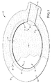
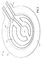
図1について説明すると、超過圧力解放装置10は、対向面16、17を含む中央破裂部14と外側フランジ18とを持つ金属部材12を有する。金属部材12は、特定の用途に適したあらゆる適切な金属又は合金で形成することができる。いくつかの実施形態では、超過圧力解放装置10は、高温又は高腐食性の用途で使用されるであろう。それらの用途では、部材12は、ステンレス鋼、インコネル、ハステロイのような耐熱性合金で形成することができる。金属部材12は、さらに、中央破裂部14から外側の半径方向に突出するタブ19を有する。金属部材12は、上記中央破裂部14が隆起領域15を有する反転動作型破裂ディスクとして図示される。そのような実施形態では、中央部14の対向面は、凹面16と凸面17とを有する。しかしながら、本発明の概念を逸脱せずに他のタイプの超過圧力解放装置を使用できることが理解されるべきである。例えば、いくつかの実施形態では、金属部材12は、(図9に示されているような)隆起した前方作動型破裂ディスク又はベントパネル、或いは平坦な破裂ディスク又はベントパネルであっても良い。
With reference to FIG. 1, the
金属部材12は、凹面16の中に形成され、かつ中央破裂部14の破裂エリアを定義する開口線20を有する。開口線20は、面16から面17に向かって伸びる深さを持つ開口線凹部22を有する。開口線20は、ほとんどあらゆる所望の形状を有することができる。しかしながら、いくつかの実施形態では、開口線20は、実質的にC字状である結果として部材12の開口時に単一の花弁状部の構成が生じても良く、又は、部材12の開口時に複数の花弁状部になるように構成された十字パターン形状であっても良い。金属部材12は、必要に応じて、開口線20に沿った又は近接した位置にあり、かつ開口線20の端23、25の間に定義されたヒンジ領域13の略反対側に位置する開口開始地点21を有することができる。開口線20は、金型分割、化学的電解研磨、機械的フライス加工、又はレーザ加工を含む、当業者に既知のあらゆるプロセスによって形成することができる。好ましくは、開口線20は、少なくとも事前隆起加工又は最終隆起加工に続いて、中央破裂部14の中に形成される。金属部材12は、さらに、中央破裂部14の内部に位置し、かつ好ましくは隆起領域15の頂点又はその近くに位置する反転開始機構(図示せず)を含むことができる。
The
装置10は、さらに、金属部材12の少なくとも一方の面の少なくとも一部に塗布された非導電膜24を有する。一般に、非導電膜24は、プロセスの流れにさらされない中央破裂部14の面に直接塗布されるが、中央破裂部14のプロセス側にも非導電膜24を塗布する希望がある場合には、それは、本発明の範囲内である。いくつかの実施形態では、膜24は、液体又はペーストとして塗布され、中間の粘着性組成物がない状態で破裂部14の面の本来の場所で硬化する。従って、膜24は、接着剤又は膜(例えば、カプトンフィルム)のような介挿材料によって破裂部14の面から分離されることがなく、膜24自身が接着剤又は事前に作製された膜を有することもない。
The
非導電膜24は、非導電ペイント、プライマ、又はインクを含むことができる。いくつかの実施形態では、膜24は、非導電エッチングプライマを有することができる。他の実施形態では、非導電膜24は、部材12に塗布され、かつ紫外線照射を通して適所で硬化する紫外線硬化性材料を含む。装置10のための多くの用途は、腐食性環境だけでなく極端な温度及び圧力状態に対する暴露を伴うので、非導電膜24は、金属部材12の表面に対する粘着力を最大化するように開発することができる。代表的な非導電膜24は、(チタン二酸化化合物のような)非導電性金属酸化物、非導電性ポリマ、セラミック、エポキシ樹脂ベースの成分、シリコーンエラストマ、又はパリレン(ポリ(パラキシリレン)ポリマ)を含むことができる。いくつかの実施形態では、非導電膜24は、インクジェット印刷技術を使用して金属部材12の表面に塗布されるが、スクリーン印刷、リソグラフィなどのような他のタイプの印刷技術を使用することができる。膜24は、図の中に示すように金属部材12の面全体に塗布することができ、又は、膜24は、後で導電インクを塗布する所望の面の所定の部分だけに選択的に塗布することができる。
The
装置10は、さらに、非導電膜24に重なる導電インク配線26を有し、非導電膜24は、金属部材12からインク配線26を物理的に分離し、かつ電気的に絶縁する。導電インク配線26は、電気信号を送信できる様々なインク又は膜を有することができる。いくつかの実施形態では、導電インクは、インクジェット印刷ヘッドを通して噴射できるようなサイズであり、かつ好ましくは1ミクロン未満の粒子サイズを持つ金属粒子を含むことができる。金属粒子は、銀、金、銅、アルミニウム、鉄、チタン、プラチナ、又はタングステンのようなあらゆる遷移金属であっても良い。これらの材料に加えて、インクは、炭素粒子のような導電非金属、或いはシリコン又はドープされたシリコンのような半導電半金属も含むことができる。この目的のために、導電ポリマインクも使用することができる。インク配線26のために使用される具体的な導電インクの選択時に考慮される1つのファクタは、装置10が実利用される時にインクが耐える必要がある温度である。インクが非導電膜に接着されたままであり、必要な最高の動作温度でのいくつかの導電特性を保持する場合には、導電インクは、ある温度に「耐える」と考えられる。好適な実施形態では、導電インクは、少なくとも400°F(204℃)、少なくとも600°F(316℃)、又は少なくとも800°F(427℃)の温度に耐えられる。代替実施形態では、導電インクは、約400°F(204℃)から約1200°F(649℃)まで、約500°F(260℃)から約1000°F(538℃)まで、又は約600°F(316℃)から約900°F(482℃)までの温度に耐えられる。もちろん、以下に記載の非導電膜24及び取捨選択できる保護膜も、特定の用途の同様な温度状態に耐えられるはずである。導電インク配線26の厚さは、インク配線26の所望の機能に応じて変えることができる。例えば、インク配線26の厚さは、インク配線26によって伝達された信号の変化を検出するために必要な所望のレベルの感度になるように変えることができる。
The
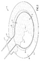
図2に示すように、インク配線26は、開口線20の全て又は少なくとも一部に重なるように、破裂部14の周囲又はその近くの非導電膜24の上に塗布することができる。膜24は、インク配線26が導線27で構成できるように、タブ19の少なくとも一部の上にも塗布することができる。図示するように、配線26は、タブ19を横切り、ヒンジ領域13を通り、開口線20に向かって伸びる。次に、配線26は、開口線20をなぞり、ヒンジ領域13向かって戻り、タブ19を横切る。本発明の範囲を逸脱せずに配線26の代替構成物が可能であることが理解される。代表的な配線の代替構成物を以下に記載する。
As shown in FIG. 2, the
図3について説明すると、部材12と開口線凹部22と導電インク配線26との関係の拡大図が示されている。この特定の実施形態では、配線26の少なくとも一部は、凹部22に直接重なり、非導電膜24によって部材12から分離される。いくつかの実施形態では、インク配線26は、凹部22の縁の内部にあり、面16よりも下方に伸びる。特定の実施形態では、配線26は、凹部22を実質的に満たすので、クラック又は破裂部14を通るピンホール漏れを検出するための手段を提供する。開口線20は、一般に、弱められたエリアを有するので、装置10の早期故障は、この領域で生じる可能性が高い。そのような故障の結果として、配線26の完全な切断が生じることがあり、その切断は、配線26を有する回路によって伝達された信号の割込みとして検出されるであろう。その代わりに、故障の結果として、配線26の変形及び回路抵抗の対応した変化が生じることがあり、その変形及び変化は、適切な感知機器によって検出できるであろう。その時、オペレータは、故障の警報を出され、装置10を取り替えるために派遣されるであろう。
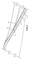
Referring to FIG. 3, an enlarged view of the relationship among the
図4は、インク配線26の別の構成を示す。この特定の実施形態では、インク配線26は、主として開口線20に隣接した位置に配置され、単に1箇所で開口線凹部22を横切る。図示するように、配線26は、開口開始地点21又はその近くで凹部22を横切る。従って、破裂部14が開口線20に沿って開口する時に配線26が切断された結果として、それによって信号の割込みが伝達されるであろう。配線26が所望の追加地点で凹部22を横切ることは、本発明の範囲内である。しかしながら、破裂部14の開口特性に対するあらゆる影響を最小化するために、配線26を切断する必要がある回数を最小化するのが望ましいかもしれない。けれども、引き裂くことに対する抵抗が非常に小さい配線構成を使用することができるので、破裂部14の開口特性に対する影響は、ほとんど無視できる。これは、低圧の用途で使用された装置という状況で非常に重要である。低圧の用途では、プロセス流体から入手可能なエネルギは、低くて、カプトンのようなポリマ薄膜から成るセンサを引き裂くには不十分であるかもしれない。従って、装置が開口するけれどもセンサ回路を切断しない、又は、ポリマ薄膜によって与えられた引き裂くことに対する抵抗の追加によって、装置の意味のある開口が完全に抑制される。そのような問題は、本発明を用いて、適切な非導電膜及び導電インクの選択並びにそれらの個々の構成を通して回避することができる。
FIG. 4 shows another configuration of the
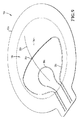
図5は、破裂部14が少なくとも2つの別個の回路配線26、30を有する本発明の他の一実施形態を示し、そのそれぞれは、個々の機能を実行するように構成される。配線26は、図1〜3と同様な漏れ検出構成で示されている。しかしながら、配線30は、ずっと手の込んだ構成を有し、抵抗の変化に基づいて(温度又は圧力のような)装置10に関連した状態を検出するのに使用することができる。配線30に対する状態の物理的影響を最大化し、それによる結果として、配線30が伝達した電気信号の最大化された変化が生じるようにするために、配線30は、配線26に比べてより長い状態で構成することができる。配線26及び30は、破裂部14の同じ部分にオーバラップする又は重なる必要がないので、それらは、単に互いに横方向に間隔を開けて配置し、非導電膜24の同じ層に重なることができる。しかしながら、以下により詳細に説明するように、いくつかの用途では、これらの配線は、破裂部14の同じ地点を横切って伸びるのが望ましいかもしれない。そのようなことは、配線の「積み重ね」、即ち配線の間に第2非導電層を介挿することによって達成することができる。
FIG. 5 shows another embodiment of the invention in which the
この更なる非導電層は、保護膜28の形態であっても良い。図6に示されるように、保護膜28は、インク配線26の上に更なる導電インク配線を塗布することを可能にすると同時に、各回路の電気的絶縁を確実にするために、インク配線26の上に塗布することができる。いくつかの実施形態では、配線26と保護膜28との間には、粘着性の層又は膜が介挿されていない。配線の「積み重ね」がない実施形態であってもなお、酸化又は他のタイプの損傷から配線26を保護する保護層として保護膜28を使用するのが望ましいかもしれない。いくつかの実施形態では、保護膜28は、高温に耐えるその能力のために選択され、かつ膜24及び配線26を粘着又は化学結合させる材料を含む。従って、保護膜26は、膜24のために使用されたものと同様の材料を含むことができる。
This further non-conductive layer may be in the form of a
非導電膜24、導電インク配線25、及び保護膜28は、全て、中央破裂部14の隆起及び開口線20の創出後に金属部材12に塗布することができる。好ましくは、これらの層の内の1つ以上は、インクジェット印刷技術を使用して塗布される。従って、これらの材料の内の少なくとも1つの材料の堆積は、三次元的な形成基板の上に生じ、インクジェット印刷で典型的な平らな膜又は表面には生じない。
The
図7及び8は、配線30の少なくとも一部が配線26の一部に重なる破裂部14を示す。この実施形態では、配線30は、配線がタブ19を横切り、ヒンジ領域13を横切り、開口地点21の近くで開口線20を横切って伸びる、実質的にU字状の構成を有する。配線30は、開口線20を横切り、かつヒンジ領域13を横切り、かつタブ19を横切って戻るように配線を導く湾曲部31を含む。いくつかの実施形態では、配線30は、例えば、装置10の動作温度の変化を検出するのに便利な熱電対を有することができる。図示するように、配線26及び30は、各回路を絶縁するために、保護膜28によって分離される。配線30自身は、保護膜の層(図示せず)によって覆うことができる。本発明の代替実施形態は、部材12の上に積み重ねられた複数の回路を提供するために、複数の交互の導電層及び非導電層を有することができる。
7 and 8 show the
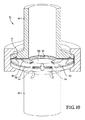
図9は、本発明の他の一実施形態に従って作製された前方作動型超過圧力解放装置10aを示す。装置10aは、金属部材12aと、中央破裂部14aの中に形成された開口線20aと、を有する。開口線20aは、破裂部14aの頂点又はその近くに位置する開口開始地点21aを持つ十字パターンとして構成される。また、前方作動型装置では凹面がプロセス流体にさらされるので、開口線20aは、破裂部14aの凸面17aに形成される。部材12aは、前述のものと同様な方法で構成された2つの導電配線26a、30aを有する。
FIG. 9 shows a forward actuated overpressure release device 10a made in accordance with another embodiment of the present invention. The device 10a includes a
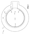
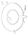
図10及び11は、本発明に係るさらに他の一実施形態を示す。いくつかの用途では、超過圧力解放装置10bは、ホルダ部材42及び44を有する保持装置40によって適所に保持される。いくつかの実施形態では、超過圧力解放装置は、支持リング45を有し、支持リング45は、部材12bのフランジ18bを支持し、かつフランジ18bと共にガスケット部材47の中に挿入される。支持リング45は、装置10bの破裂時に金属部材12bの第1開口地点21bに接触するように構成された歯50を有する。ホルダ部材42及び44の内の少なくとも一方は、一体型の開いた電気回路で構成され、開いた電気回路は、ホルダ部材の間に装置10bを固定した時に金属部材12bによって担持された1つ以上の配線によって閉じられるように構成される。従って、感知回路は、装置10bの設置時に適切な回路に自動的に接続され、それによって、装置10bが取り替えられるたびに更なる人員が周辺の電子部品を別々に接続する必要性を排除する。
10 and 11 show still another embodiment according to the present invention. In some applications, the
いくつかの実施形態では、ホルダ42は、電気回路を閉じるために、金属部材12bの上の対応する端子52、54に係合するように構成された電気接点46、48を有する。金属部材が複数の導電配線を有する実施形態では、同様な構成を使用することができる。そのような実施形態では、ホルダ42は、複数の開いた電気回路と、ホルダの間に圧力解放装置を固定する時に閉じられるように構成された対応する接点と、を有することができる。
In some embodiments, the
ホルダ42によって担持された電気接点46、48は、あらゆる数の代替構成物を有することができる。しかしながら、図示するように、接点46、48は、平坦な解放装置の係合表面56から突出する一対のピンを有する。端子52、54は、フランジ18bを通って接点46、48が挿入される一対の開口を有する。従って、接点46、48は、端子52、54に係合する手段を提供するだけでなく、装置10bがホルダ部材42と44との間に設置された時に適切な方向に配置されることも確実にする。ホルダ部材42、44の内の一方の内部に電気接点を一体化する他の手段が可能であり、前述の説明は、本発明の範囲を限定するものとみなされるべきではない。代替構成物は、回路基板又はLCDディスプレイのアセンブリの中に一般的に使用されるエラストマ材料を含む「縞模様のある」帯板の使用を含むことができる。
The
Claims (26)
前記金属部材の前記対向面の内の一方の面の少なくとも一部に塗布された非導電膜と、
前記非導電膜の少なくとも一部の上に塗布され、前記非導電膜によって前記金属部材から電気的に絶縁され、電気信号を伝導できる電気回路を定義する導電インク配線と、を有する超過圧力解放装置であって、
前記電気回路は、前記超過圧力解放装置に関連したプロセス状態の変化を検出するように動作可能である超過圧力解放装置。 A metal member having a central rupture portion and an outer flange portion surrounding the central rupture portion, and having a pair of opposing surfaces;
A non-conductive film applied to at least a part of one of the opposing surfaces of the metal member;
An overpressure relief device comprising: a conductive ink wire that is applied over at least a portion of the non-conductive film, is electrically insulated from the metal member by the non-conductive film, and defines an electrical circuit capable of conducting an electrical signal. Because
The overpressure release device is operable to detect a change in process state associated with the overpressure release device.
前記開口線凹部は、少なくとも一部が前記中央破裂部の超過圧力解放エリアを定義する請求項1に記載の超過圧力解放装置。 Furthermore, it is located inside the central rupture portion, and has an opening line recess formed on the one surface that supports the non-conductive film,
The overpressure release device according to claim 1, wherein at least a part of the opening line recess defines an overpressure release area of the central rupture portion.
前記一対の対向面は、凸面と凹面とを有する請求項1に記載の超過圧力解放装置。 The central rupture is raised;
The overpressure release device according to claim 1, wherein the pair of opposed surfaces have a convex surface and a concave surface.
前記非導電膜は、前記凹面に塗布される請求項10に記載の超過圧力解放装置。 The metal member is a reversible actuating rupture disc;
The overpressure release device according to claim 10, wherein the non-conductive film is applied to the concave surface.
前記金属部材によって担持され、かつ前記対向面の内の一方の面に形成された少なくとも第1及び第2導電回路と、を有する超過圧力解放装置であって、
前記第1及び第2導電回路のそれぞれは、電気信号を伝導でき、かつ前記超過圧力解放装置に関連したプロセス状態の変化を検出するように動作可能であり、
前記第1導電回路は、前記対向面の内の前記一方の面の少なくとも一部に直接塗布された非導電膜と、前記非導電膜の少なくとも一部の上に塗布され、かつ前記非導電膜によって前記金属部材から電気的に絶縁された第1導電インク配線と、を有し、
前記第2導電回路は、前記金属部材、及び前記第1及び第2導電回路の内の少なくとも一方の導電回路から電気的に絶縁された第2導電インク配線を有する超過圧力解放装置。 A metal member having a central rupture portion and an outer flange portion surrounding the central rupture portion, and having a pair of opposing surfaces;
An overpressure relief device comprising at least first and second conductive circuits carried by the metal member and formed on one of the opposing surfaces;
Each of the first and second conductive circuits is capable of conducting an electrical signal and is operable to detect a change in process state associated with the overpressure relief device;
The first conductive circuit is applied to at least a part of the one of the opposing surfaces, a non-conductive film directly applied to at least a part of the non-conductive film, and the non-conductive film A first conductive ink wiring electrically insulated from the metal member by
The second conductive circuit includes an overpressure release device having a second conductive ink wiring electrically insulated from at least one of the metal member and the first and second conductive circuits.
前記開口線凹部は、少なくとも一部が前記中央破裂部の超過圧力解放エリアを定義する請求項14に記載の超過圧力解放装置。 The metal member further has an opening line recess located inside the central rupture portion,
The overpressure relief device according to claim 14, wherein the open line recess at least partially defines an overpressure release area of the central rupture portion.
前記第2導電インク配線は、前記第1金属部品と異なる第2金属部品を有する請求項14に記載の超過圧力解放装置。 The first conductive ink wiring has a first metal component,
The overpressure release device according to claim 14, wherein the second conductive ink wiring has a second metal part different from the first metal part.
前記装置は、間に請求項1に記載の超過圧力解放装置を収容して固定するように構成された第1及び第2ホルダ部材を有し、
前記第1及び第2ホルダ部材の内の少なくとも一方のホルダ部材は、前記第1及び第2ホルダ部材の間に固定された時に前記超過圧力解放装置によって閉じられるように構成された開いた電気回路を有する装置。 A device for holding an overpressure release device,
The device has first and second holder members configured to receive and secure the overpressure release device of claim 1 in between,
An open electrical circuit configured such that at least one of the first and second holder members is closed by the overpressure release device when secured between the first and second holder members. Having a device.
前記超過圧力解放装置は、
中央破裂部と前記中央破裂部を取り囲む関係にある外側フランジ部とを有し、かつ一対の対向面を持つ金属部材と、
前記金属部材の前記対向面の内の一方の面の少なくとも一部に塗布された非導電膜と、
前記非導電膜の少なくとも一部の上に塗布され、かつ前記非導電膜によって前記金属部材から電気的に絶縁され、かつ電気信号を伝導できる電気回路を定義する導電インク配線と、を有し、
前記電気回路は、前記超過圧力解放装置に関連したプロセス状態の変化を検出するように動作可能であり、
前記第1及び第2ホルダ部材の内の少なくとも一方のホルダ部材は、前記第1及び第2ホルダ部材の間に固定された時に前記超過圧力解放装置によって閉じられるように構成された開いた電気回路を有する組み合わせ。 An overpressure release device, and a combination of first and second holder members configured to receive and secure the overpressure release device therebetween,
The overpressure release device includes:
A metal member having a central rupture portion and an outer flange portion surrounding the central rupture portion, and having a pair of opposing surfaces;
A non-conductive film applied to at least a part of one of the opposing surfaces of the metal member;
A conductive ink wiring that is applied over at least a portion of the non-conductive film and that is electrically insulated from the metal member by the non-conductive film and that defines an electrical circuit capable of conducting an electrical signal;
The electrical circuit is operable to detect a change in a process state associated with the overpressure relief device;
An open electrical circuit configured such that at least one of the first and second holder members is closed by the overpressure release device when secured between the first and second holder members. A combination with
Applications Claiming Priority (3)
| Application Number | Priority Date | Filing Date | Title |
|---|---|---|---|
| US201462047377P | 2014-09-08 | 2014-09-08 | |
| US62/047,377 | 2014-09-08 | ||
| PCT/US2015/048867 WO2016040277A1 (en) | 2014-09-08 | 2015-09-08 | Pressure relief device having conductive ink sensors formed thereon |
Publications (2)
| Publication Number | Publication Date |
|---|---|
| JP2017526880A true JP2017526880A (en) | 2017-09-14 |
| JP2017526880A5 JP2017526880A5 (en) | 2018-09-27 |
Family
ID=55437150
Family Applications (1)
| Application Number | Title | Priority Date | Filing Date |
|---|---|---|---|
| JP2017512738A Pending JP2017526880A (en) | 2014-09-08 | 2015-09-08 | Pressure release device with conductive ink sensor formed thereon |
Country Status (6)
| Country | Link |
|---|---|
| US (1) | US20160069474A1 (en) |
| EP (1) | EP3191750A4 (en) |
| JP (1) | JP2017526880A (en) |
| CN (1) | CN106715987A (en) |
| CA (1) | CA2960106A1 (en) |
| WO (1) | WO2016040277A1 (en) |
Families Citing this family (7)
| Publication number | Priority date | Publication date | Assignee | Title |
|---|---|---|---|---|
| CA2946199C (en) * | 2014-04-17 | 2021-12-28 | Fike Corporation | Reverse-acting rupture disc with buckling-control feature |
| BR112018009132A8 (en) | 2015-11-06 | 2019-02-26 | Oklahoma Safety Equipment Company Inc | rupture disc device and mounting method |
| EP3415759B1 (en) * | 2017-06-13 | 2020-12-02 | SISTO Armaturen S.A. | Membrane with conductive structures |
| CN108253173A (en) * | 2018-02-26 | 2018-07-06 | 大连理工安全技术与控制工程研究中心有限公司 | A kind of automatic Prediction service life and the rupture disk safety device for replacing early warning in real time |
| DE102018119144A1 (en) * | 2018-08-07 | 2020-02-13 | R. Stahl Schaltgeräte GmbH | Pressure relief device and housing with such |
| DE102020101176A1 (en) * | 2020-01-20 | 2021-07-22 | Sisto Armaturen S.A. | Machine-readable identification of a membrane |
| DE102020101394A1 (en) * | 2020-01-22 | 2021-07-22 | Sisto Armaturen S.A. | Membrane with machine-readable identification on the membrane flap |
Family Cites Families (29)
| Publication number | Priority date | Publication date | Assignee | Title |
|---|---|---|---|---|
| US3088478A (en) * | 1960-02-29 | 1963-05-07 | Mcdonnell Aircraft Corp | Valve device |
| US4342988A (en) * | 1980-01-25 | 1982-08-03 | Continental Disc Corporation | Rupture disc alarm system |
| US4408194A (en) * | 1981-02-02 | 1983-10-04 | Continental Disc Corporation | Capacitive pressure relief rupture disc monitor |
| US4787825A (en) * | 1984-09-27 | 1988-11-29 | Myron Mantell | Failure sensing device for a diaphragm pump |
| US4781535A (en) * | 1987-11-13 | 1988-11-01 | Pulsafeeder, Inc. | Apparatus and method for sensing diaphragm failures in reciprocating pumps |
| US4813564A (en) * | 1988-02-25 | 1989-03-21 | Westinghouse Electric Corp. | Package |
| US4978947A (en) * | 1989-05-25 | 1990-12-18 | Bs&B Safety Systems, Inc. | Rupturable fluid flow indicator |
| US5155471A (en) * | 1991-06-21 | 1992-10-13 | Bs&B Safety Systems, Inc. | Low pressure burst disk sensor with weakened conductive strips |
| DE4140089A1 (en) * | 1991-12-05 | 1993-06-09 | Hoechst Ag, 6230 Frankfurt, De | Rupture disc |
| US5313194A (en) * | 1992-04-14 | 1994-05-17 | Varos Richard V | Rupture disk sensing assembly |
| US5631634A (en) * | 1995-01-11 | 1997-05-20 | Oklahoma Safety Equipment Co. | Flow and pressure sensor |
| US5755249A (en) * | 1995-03-15 | 1998-05-26 | Process Equipment Limited | Fluid flow monitor |
| US5602372A (en) * | 1995-12-01 | 1997-02-11 | Oklahoma Safety Equipment Co. | Differential pressure flow sensor |
| US5661277A (en) * | 1995-12-01 | 1997-08-26 | Oklahoma Safety Equipment Co. | Differential pressure flow sensor using multiple layers of flexible membranes |
| US6680016B2 (en) * | 2001-08-17 | 2004-01-20 | University Of Dayton | Method of forming conductive polymeric nanocomposite materials |
| EP1669830B1 (en) * | 2001-08-24 | 2019-10-09 | BS & B Safety Systems Limited | Monitoring system for a pressurized container |
| US6964205B2 (en) * | 2003-12-30 | 2005-11-15 | Tekscan Incorporated | Sensor with plurality of sensor elements arranged with respect to a substrate |
| US7921727B2 (en) * | 2004-06-25 | 2011-04-12 | University Of Dayton | Sensing system for monitoring the structural health of composite structures |
| US7600527B2 (en) * | 2005-04-01 | 2009-10-13 | Fike Corporation | Reverse acting rupture disc with laser-defined electropolished line of weakness and method of forming the line of weakness |
| KR100735411B1 (en) * | 2005-12-07 | 2007-07-04 | 삼성전기주식회사 | Method For Forming Printed Wiring Board and Printed Wiring Board Thus Obtained |
| US7567183B2 (en) * | 2006-01-06 | 2009-07-28 | Exatec Llc | Printable sensors for plastic glazing |
| US7950289B2 (en) * | 2006-02-03 | 2011-05-31 | Bae Systems Plc | Damage sensors |
| JP2007257869A (en) * | 2006-03-20 | 2007-10-04 | Mitsui Mining & Smelting Co Ltd | Conductive ink |
| GB201004224D0 (en) * | 2010-03-15 | 2010-04-28 | Rolls Royce Plc | A strain assembly and method |
| US8354934B2 (en) * | 2010-06-14 | 2013-01-15 | Fike Corporation | Burst indicator |
| CN102401162B (en) * | 2010-09-19 | 2013-12-25 | 上海华理安全装备有限公司 | Temperature and pressure dual acting explosion-proof device |
| CN202852109U (en) * | 2012-10-29 | 2013-04-03 | 成都凯天电子股份有限公司 | Super-pressure preventing relief safety device |
| US8828503B1 (en) * | 2013-02-28 | 2014-09-09 | Eastman Kodak Company | Making multi-layer micro-wire structure |
| WO2015025680A1 (en) * | 2013-08-23 | 2015-02-26 | アルプス電気株式会社 | Capacitance-type input device |
-
2015
- 2015-09-08 US US14/847,702 patent/US20160069474A1/en not_active Abandoned
- 2015-09-08 EP EP15839536.8A patent/EP3191750A4/en not_active Withdrawn
- 2015-09-08 CA CA2960106A patent/CA2960106A1/en not_active Abandoned
- 2015-09-08 WO PCT/US2015/048867 patent/WO2016040277A1/en active Application Filing
- 2015-09-08 JP JP2017512738A patent/JP2017526880A/en active Pending
- 2015-09-08 CN CN201580048019.6A patent/CN106715987A/en active Pending
Also Published As
| Publication number | Publication date |
|---|---|
| EP3191750A4 (en) | 2018-05-23 |
| WO2016040277A1 (en) | 2016-03-17 |
| EP3191750A1 (en) | 2017-07-19 |
| CN106715987A (en) | 2017-05-24 |
| CA2960106A1 (en) | 2016-03-17 |
| US20160069474A1 (en) | 2016-03-10 |
Similar Documents
| Publication | Publication Date | Title |
|---|---|---|
| JP2017526880A (en) | Pressure release device with conductive ink sensor formed thereon | |
| TWI617943B (en) | Security wrap with tearable substrate | |
| CA2802457C (en) | Burst indicator | |
| JPH05187896A (en) | Apparatus for sensing flow rate in very-low- pressure flow line | |
| US4978947A (en) | Rupturable fluid flow indicator | |
| JP3807498B2 (en) | Gasket for fuel cell | |
| JP5911984B2 (en) | Heat exchanger plate and plate heat exchanger | |
| EP2459911B1 (en) | Pressure relief device integrity sensor | |
| JPH01142284A (en) | Device and method of detecting trouble of diaphragm of pump | |
| JP2018520484A (en) | Adjustable heater | |
| JP3201524B2 (en) | Rupture disc sensing assembly | |
| JP2013538990A5 (en) | ||
| KR20110053704A (en) | Pipe leak/burst sensing apparatus | |
| JP2017526880A5 (en) | ||
| DK148428B (en) | LEVEL DETECTOR WITH A PIEZOELECTRIC CRYSTAL |
Legal Events
| Date | Code | Title | Description |
|---|---|---|---|
| A521 | Written amendment |
Free format text: JAPANESE INTERMEDIATE CODE: A523 Effective date: 20180814 |
|
| A621 | Written request for application examination |
Free format text: JAPANESE INTERMEDIATE CODE: A621 Effective date: 20180814 |
|
| A977 | Report on retrieval |
Free format text: JAPANESE INTERMEDIATE CODE: A971007 Effective date: 20190530 |
|
| A131 | Notification of reasons for refusal |
Free format text: JAPANESE INTERMEDIATE CODE: A131 Effective date: 20190604 |
|
| A02 | Decision of refusal |
Free format text: JAPANESE INTERMEDIATE CODE: A02 Effective date: 20200107 |