JP2017520083A - Bus bar for electric device and window glass including the same - Google Patents
Bus bar for electric device and window glass including the same Download PDFInfo
- Publication number
- JP2017520083A JP2017520083A JP2016565177A JP2016565177A JP2017520083A JP 2017520083 A JP2017520083 A JP 2017520083A JP 2016565177 A JP2016565177 A JP 2016565177A JP 2016565177 A JP2016565177 A JP 2016565177A JP 2017520083 A JP2017520083 A JP 2017520083A
- Authority
- JP
- Japan
- Prior art keywords
- bus bar
- layer
- substrate
- conductive material
- grid line
- Prior art date
- Legal status (The legal status is an assumption and is not a legal conclusion. Google has not performed a legal analysis and makes no representation as to the accuracy of the status listed.)
- Pending
Links
Images


Classifications
-
- B—PERFORMING OPERATIONS; TRANSPORTING
- B60—VEHICLES IN GENERAL
- B60S—SERVICING, CLEANING, REPAIRING, SUPPORTING, LIFTING, OR MANOEUVRING OF VEHICLES, NOT OTHERWISE PROVIDED FOR
- B60S1/00—Cleaning of vehicles
- B60S1/02—Cleaning windscreens, windows or optical devices
- B60S1/023—Cleaning windscreens, windows or optical devices including defroster or demisting means
- B60S1/026—Cleaning windscreens, windows or optical devices including defroster or demisting means using electrical means
-
- H—ELECTRICITY
- H01—ELECTRIC ELEMENTS
- H01C—RESISTORS
- H01C17/00—Apparatus or processes specially adapted for manufacturing resistors
- H01C17/06—Apparatus or processes specially adapted for manufacturing resistors adapted for coating resistive material on a base
-
- H—ELECTRICITY
- H01—ELECTRIC ELEMENTS
- H01C—RESISTORS
- H01C17/00—Apparatus or processes specially adapted for manufacturing resistors
- H01C17/28—Apparatus or processes specially adapted for manufacturing resistors adapted for applying terminals
-
- H—ELECTRICITY
- H01—ELECTRIC ELEMENTS
- H01C—RESISTORS
- H01C17/00—Apparatus or processes specially adapted for manufacturing resistors
- H01C17/30—Apparatus or processes specially adapted for manufacturing resistors adapted for baking
-
- H—ELECTRICITY
- H05—ELECTRIC TECHNIQUES NOT OTHERWISE PROVIDED FOR
- H05B—ELECTRIC HEATING; ELECTRIC LIGHT SOURCES NOT OTHERWISE PROVIDED FOR; CIRCUIT ARRANGEMENTS FOR ELECTRIC LIGHT SOURCES, IN GENERAL
- H05B3/00—Ohmic-resistance heating
- H05B3/84—Heating arrangements specially adapted for transparent or reflecting areas, e.g. for demisting or de-icing windows, mirrors or vehicle windshields
-
- H—ELECTRICITY
- H05—ELECTRIC TECHNIQUES NOT OTHERWISE PROVIDED FOR
- H05B—ELECTRIC HEATING; ELECTRIC LIGHT SOURCES NOT OTHERWISE PROVIDED FOR; CIRCUIT ARRANGEMENTS FOR ELECTRIC LIGHT SOURCES, IN GENERAL
- H05B2203/00—Aspects relating to Ohmic resistive heating covered by group H05B3/00
- H05B2203/011—Heaters using laterally extending conductive material as connecting means
-
- H—ELECTRICITY
- H05—ELECTRIC TECHNIQUES NOT OTHERWISE PROVIDED FOR
- H05B—ELECTRIC HEATING; ELECTRIC LIGHT SOURCES NOT OTHERWISE PROVIDED FOR; CIRCUIT ARRANGEMENTS FOR ELECTRIC LIGHT SOURCES, IN GENERAL
- H05B2203/00—Aspects relating to Ohmic resistive heating covered by group H05B3/00
- H05B2203/013—Heaters using resistive films or coatings
-
- H—ELECTRICITY
- H05—ELECTRIC TECHNIQUES NOT OTHERWISE PROVIDED FOR
- H05B—ELECTRIC HEATING; ELECTRIC LIGHT SOURCES NOT OTHERWISE PROVIDED FOR; CIRCUIT ARRANGEMENTS FOR ELECTRIC LIGHT SOURCES, IN GENERAL
- H05B2203/00—Aspects relating to Ohmic resistive heating covered by group H05B3/00
- H05B2203/016—Heaters using particular connecting means
-
- H—ELECTRICITY
- H05—ELECTRIC TECHNIQUES NOT OTHERWISE PROVIDED FOR
- H05B—ELECTRIC HEATING; ELECTRIC LIGHT SOURCES NOT OTHERWISE PROVIDED FOR; CIRCUIT ARRANGEMENTS FOR ELECTRIC LIGHT SOURCES, IN GENERAL
- H05B2203/00—Aspects relating to Ohmic resistive heating covered by group H05B3/00
- H05B2203/017—Manufacturing methods or apparatus for heaters
-
- Y—GENERAL TAGGING OF NEW TECHNOLOGICAL DEVELOPMENTS; GENERAL TAGGING OF CROSS-SECTIONAL TECHNOLOGIES SPANNING OVER SEVERAL SECTIONS OF THE IPC; TECHNICAL SUBJECTS COVERED BY FORMER USPC CROSS-REFERENCE ART COLLECTIONS [XRACs] AND DIGESTS
- Y10—TECHNICAL SUBJECTS COVERED BY FORMER USPC
- Y10T—TECHNICAL SUBJECTS COVERED BY FORMER US CLASSIFICATION
- Y10T29/00—Metal working
- Y10T29/49—Method of mechanical manufacture
- Y10T29/49002—Electrical device making
- Y10T29/49082—Resistor making
- Y10T29/49085—Thermally variable
Abstract
窓ガラスは、昼光開口部を有し、第1表面を有する基板を含む。窓ガラスは電気装置を更に含み、電気装置は、導電材料をそれぞれ独立して含む第1バスバー、第2バスバー及びグリッドライン部を含む。グリッドライン部は、第1バスバーに動作的に接続され且つ接する第1端及び第2バスバーに動作的に接続され且つ接する第2端を有する。グリッドライン長さは、グリッドライン部の第1端及び第2端の間に画定される。グリッドライン部は、グリッドライン長さに沿って第1表面上に完全且つ直接的に配置される。第1バスバー及び第2バスバーは、基板上に配置された導電材料の第1層をそれぞれ独立して含む。第1バスバー及び第2バスバーのうちの少なくとも一つは、第1層上に配置された導電材料の第2層をそれぞれ独立して含む。The window glass includes a substrate having a daylight opening and having a first surface. The window glass further includes an electrical device, and the electrical device includes a first bus bar, a second bus bar, and a grid line portion, each of which includes a conductive material independently. The grid line portion has a first end operatively connected to and in contact with the first bus bar and a second end operatively connected to and in contact with the second bus bar. The grid line length is defined between the first end and the second end of the grid line portion. The grid line portion is completely and directly disposed on the first surface along the grid line length. The first bus bar and the second bus bar each independently include a first layer of conductive material disposed on the substrate. At least one of the first bus bar and the second bus bar independently includes a second layer of conductive material disposed on the first layer.
Description
[関連出願の相互参照]
本出願は、2014年4月30日に出願された、米国仮特許出願第61/986,534号に対する優先権及びその全ての利益を主張する。当該米国仮出願は、その全体について参照により本明細書に明示的に組み込まれる。
[Cross-reference of related applications]
This application claims priority to US Provisional Patent Application No. 61 / 986,534, filed Apr. 30, 2014, and all its benefits. The provisional application is expressly incorporated herein by reference in its entirety.
本開示は、概して電気装置を有する窓ガラス(window pane)に関し、より具体的には、電気装置のバスバー(busbar)に関する。 The present disclosure relates generally to window panes having electrical devices, and more specifically to electrical device busbars.
車両(vehicle)用の窓ガラスは、窓ガラスから結露を取り除き、霜を解かすためのデフロスタやデフォッガ等の電気装置を含み得る。電気装置は、窓ガラス内又は窓ガラス上に導電材料(conductive materials)を典型的に含む。電流は、一対の離間したバスバーによって電気装置の導電材料に供給される。バスバーは、電気装置が適切に機能するために要求される電流の量を流すのに適していなければならない。典型的には、従来のバスバーは、電気装置に必要とされる電流の量に対応するために、少なくとも12mmの幅を有する。 A window glass for a vehicle may include an electrical device such as a defroster or a defogger for removing condensation from the window glass and defrosting it. Electrical devices typically include conductive materials in or on the glazing. Current is supplied to the conductive material of the electrical device by a pair of spaced bus bars. The bus bar must be suitable to carry the amount of current required for the electrical device to function properly. Typically, conventional bus bars have a width of at least 12 mm to accommodate the amount of current required for electrical devices.
バスバーのそれぞれに沿って延びる導電編組(conductive braid)(端子編組としても知られている)は、典型的に、電気装置を通って伝導される電流の量を増加させるために電気装置において利用される。しかしながら、導電編組がバスバーと電気的に通じる(in electrical communication)ように導電編組をバスバーに動作的に接続する(operatively connect)ためには、多数のはんだ接合が要求される。この導電編組は、バスバーと共に利用される場合、はんだ付け不良の発生に起因する歩留まり低下、及び、導電編組をバスバーに動作的に接続するために要求される多数のはんだ接合の使用に起因する生産時間及び費用の増加を、結果として生じさせる。したがって、改善されたバスバー及び窓ガラスを提供する必要性が依然として存在する。 Conductive braids (also known as terminal braids) that extend along each of the busbars are typically utilized in electrical devices to increase the amount of current conducted through the electrical device. The However, multiple solder joints are required to operatively connect the conductive braid to the bus bar so that the conductive braid is in electrical communication with the bus bar. When used with bus bars, this conductive braid reduces production due to poor soldering and production due to the use of multiple solder joints required to operably connect the conductive braid to the bus bar. An increase in time and costs results. Accordingly, there remains a need to provide improved busbars and glazing.
本開示は、昼光開口部を有する窓ガラスを提供する。窓ガラスは、第1表面及び第1表面の反対側の第2表面を有する基板を含む。窓ガラスは、第1バスバー、第2バスバー及びグリッドライン部を含む電気装置であり、第1バスバー、第2バスバー及びグリッドライン部は、導電材料をそれぞれ独立して含む、電気装置、を更に含む。第1バスバー、第2バスバー及びグリッドライン部は、互いに電気的に通じている。第1バスバーは、基板上に配置されている。第2バスバーは、第1バスバーから離間して基板上に配置されている。グリッドライン部は、第1バスバーに動作的に接続され且つ接する第1端及び第2バスバーに動作的に接続され且つ接する第2端を有する。グリッドライン長さは、グリッドライン部の第1端及び前記第2端の間に画定される。グリッドライン部は、グリッドライン長さに沿って基板の第1表面上に完全且つ直接的に配置される。第1バスバー及び第2バスバーは、基板上に配置された導電材料の第1層をそれぞれ独立して含む。第1バスバー及び第2バスバーの少なくとも一つは、第1層上に配置された導電材料の第2層をそれぞれ独立して含む。グリッドライン部は、導電材料の第1層又は導電材料の第2層の一つを含む。第1層及び第2層の導電材料は、同じであるか又は異なっている。 The present disclosure provides a glazing having a daylight opening. The glazing includes a substrate having a first surface and a second surface opposite the first surface. The window glass is an electric device including a first bus bar, a second bus bar, and a grid line portion, and the first bus bar, the second bus bar, and the grid line portion further include an electric device that includes a conductive material independently. . The first bus bar, the second bus bar, and the grid line portion are in electrical communication with each other. The first bus bar is disposed on the substrate. The second bus bar is disposed on the substrate apart from the first bus bar. The grid line portion has a first end operatively connected to and in contact with the first bus bar and a second end operatively connected to and in contact with the second bus bar. The grid line length is defined between the first end and the second end of the grid line portion. The grid line portion is completely and directly disposed on the first surface of the substrate along the grid line length. The first bus bar and the second bus bar each independently include a first layer of conductive material disposed on the substrate. At least one of the first bus bar and the second bus bar independently includes a second layer of conductive material disposed on the first layer. The grid line portion includes one of a first layer of conductive material or a second layer of conductive material. The conductive material of the first layer and the second layer is the same or different.
本開示は、窓ガラスを形成するための方法を更に提供する。方法は、基板を提供するステップを含む。方法はまた、基板上に第1導電組成物を配置し、第1バスバー及び第2バスバーの導電材料の第1層を形成するステップを含む。方法は、第1バスバー及び第2バスバーのうちの少なくとも一つの導電材料の第1層上に、第1導電組成物と同じであるか又は異なっている、第2導電組成物を配置し、第1バスバー及び第2バスバーのうちの少なくとも一つの導電材料の第2層を形成するステップを更に含む。グリッドライン部は、基板上に配置される。グリッドライン部は、第1導電組成物を配置するステップで形成されるか又は第2導電組成物を配置するステップで形成される。 The present disclosure further provides a method for forming a glazing. The method includes providing a substrate. The method also includes disposing a first conductive composition on the substrate to form a first layer of conductive material for the first bus bar and the second bus bar. The method includes disposing a second conductive composition on the first layer of at least one of the first bus bar and the second bus bar that is the same as or different from the first conductive composition; The method further includes forming a second layer of the conductive material of at least one of the first bus bar and the second bus bar. The grid line part is disposed on the substrate. The grid line portion is formed in the step of arranging the first conductive composition or formed in the step of arranging the second conductive composition.
本開示の利点は、添付の図面に関連して検討されるときに以下の詳細な説明への参照によってより良く理解されるに従って、容易に理解されるであろう。 The advantages of the present disclosure will be readily understood as the same becomes better understood by reference to the following detailed description when considered in conjunction with the accompanying drawings.
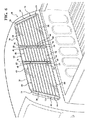
本開示は、窓ガラス30に関する。図面を参照すると、同様の番号は図全体にわたって同様の又は対応する部分を示し、窓ガラス30の適切な実施例が図1,3及び5−24に大まかに示されている。いくつかの実施形態において、窓ガラス30は、車両用である。窓ガラス30は、典型的に光に対して光学的に透過性の昼光開口部(デイライトオープニング,daylight opening)32を有する。窓ガラス30は、基板(substrate)34を含み、基板34は、第1表面36及び第1表面36の反対側の第2表面38を有する。
The present disclosure relates to a
基板34は、ガラス、プラスチック、ポリカーボネート、アクリル及びそれらの組み合わせを含んでもよい。一つの実施形態において、基板34はガラスを含む。典型的に、ガラスは、車両用の自動車ガラスとして更に規定される(defined)。ガラスはまた、ソーダ石灰シリカベースのガラスとして更に規定されてもよい。しかしながら、ガラスは当技術分野で知られる如何なる種類のガラス、例えばホウケイ酸ガラスであってもよいことが明確に理解されるべきである。基板34は、被覆ガラスのように被覆されていてもよいことが明確に理解されるべきである。基板34は、第1表面36と第2表面38との間に配置され、基板34の周囲に沿って且つ基板34の周囲を囲むように延びるエッジを有する。基板34の第1表面36は、基板34のエッジによって画定される領域を有する。様々な実施形態において、基板34の第1表面36は、第1側部40、及び第1側部40から離間した第2側部42を有する。
The
図1,3,5−8,及び14−24に示されるように、いくつかの実施形態において、基板34はまた、基板34の第1表面36上に配置されたセラミックフリット層(ceramic frit layer)44を有する。以下では、基板34のセラミックフリット層44を含む窓ガラス30の実施形態において、基板34を指す如何なる記述も、セラミックフリット層44を指すことがあり、そのため、基板34上の構成要素の配置もまた、セラミックフリット層44上の同じ構成要素の配置を含み得ることが、明確に理解されるべきである。さらに、同じ構成要素はまた、基板34上に配置されたそれ自体の一部分と、セラミックフリット層44に配置された残りの部分とを有してもよい。
As shown in FIGS. 1, 3, 5-8, and 14-24, in some embodiments, the
特に図1,3,5及び24を参照すると、一つの実施形態において、基板34のセラミックフリット層44は、基板34の周囲に配置され、昼光開口部32を画定する。典型的に、本実施形態において、セラミックフリット層44は、基板34の周囲から第1表面36の内部に向かって部分的に内側に延びている。様々な実施形態において、基板34の周囲に配置されたセラミックフリット層44を含む窓ガラス30は、車両の後部窓46用である。後部窓46を有する適切な車両の非限定的な例は、セダン、クーペ、スポーツユーティリティ車(SUV)、クロスオーバSUV、ピックアップトラック等を含む。
With particular reference to FIGS. 1, 3, 5 and 24, in one embodiment, the
特に図6−8を参照すると、他の実施形態において、セラミックフリット層44は、基板34の第1側部40及び基板34の第2側部42に配置されている。典型的に、本実施形態において、セラミックフリット層44は、基板34の第1及び第2側部40,42のそれぞれから第1表面36の内部に向かって部分的に内側に延びている。様々な実施形態において、基板34の第1及び第2側部40,42に配置されたセラミックフリット層44を含む窓ガラス30は、車両の引窓組立体48(sliding window assembly)用である。引窓組立体48を有する適切な車両の非限定的な例は、ピックアップトラック等を含む。
With particular reference to FIGS. 6-8, in another embodiment, the
引窓組立体48は、少なくとも一枚の固定パネル50及び一枚のスライドパネル(sliding
panel)52を含む。典型的に、引窓組立体48は、二枚の固定パネル50及び一枚のスライドパネル52を含む。スライドパネル52は、開位置と閉位置との間を固定パネル50に対して移動する。スライドパネル52は、典型的に、固定パネル50に対して水平に移動する。しかしながら、スライドパネル52は如何なる他の適切な方向に、例えば垂直に移動してもよいことが、明確に理解されるべきである。いくつかの実施形態において、窓ガラス30は、固定パネル50及びスライドパネル52の両方として利用される。しかしながら、窓ガラス30は、固定パネル50又はスライドパネル52のうちの一方のみとして利用されてもよいことが、明確に理解されるべきである。
The sliding
panel) 52. Typically, the sliding
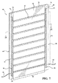
窓ガラス30は、電気装置54を更に含む。電気装置54は、加熱グリッド、アンテナグリッド又はそれらの組み合わせであってもよい。加熱グリッドは、一般的に、当技術分野においてデフロスタ又はデフォッガとも呼ばれる。電気装置54は、基板34の一つの区域の周りに配置されてもよい。典型的に、電気装置54は、基板34上に配置される。しかしながら、電気装置54は、基板34内に配置されてもよいことが、明確に理解されるべきである;例えば、基板34は、電気装置54が基板34内に埋め込まれるように形成されてもよい。一つの実施形態において、電気装置54は、基板34上に且つ実質的に基板34の周りに配置される。用語“実質的に周りに”は、本明細書において電気装置54を参照して用いられる場合、電気装置54が、基板34の領域の少なくとも50%、代替的に少なくとも60%、代替的に少なくとも70%、代替的に少なくとも80%、代替的に少なくとも90%、代替的に少なくとも95%にわたって配置されていることを指す。例えば、電気装置54が窓ガラス30用の加熱グリッドである場合に、加熱グリッドは、基板34上且つ実質的に基板34の周りに配置される。
The
図3,5,6−23を参照すると、電気装置54は、互いに電気的に通じている第1バスバー56、第2バスバー58及びグリッドライン部60を含む。いくつかの実施形態において、第1バスバー56及び第2バスバー58は、エネルギー源からグラウンドに電流を伝導する。様々な実施形態において、電気装置54は加熱グリッドである。例えば、電気装置54が自動車ガラス用の加熱グリッドである場合に、第1バスバー56は車両内のエネルギー源(例えば、電池又はオルタネータ)から電流を受け、電流をグリッドライン部60に伝導する。この例を続けると、グリッドライン部60は次いで電流を第2バスバー58に伝導し、第2バスバー58は次いで電流を車両内のグラウンドに(例えば電池に)伝導する。代わりに電流は、第2バスバー58から第1バスバー56に流れてもよいことが、明確に理解されるべきである。
Referring to FIGS. 3, 5, 6-23, the
特に図8を参照すると、いくつかの実施形態において、電気装置54は、第1バスバー56、第2バスバー58及びグリッドライン部60と電気的に通じている第3バスバー62を更に含む。一つの実施形態において、第1バスバー56、第3バスバー62は、電流をエネルギー源からグラウンドに伝導する。例えば、電気装置54が自動車ガラス用の加熱グリッドである場合に、第1バスバー56は車両内のエネルギー源(例えば、電池又はオルタネータ)から電流を受け、電流をグリッドライン部60に伝導する。この例を続けると、グリッドライン部60は次いで電流を第2バスバー58に伝導し、第2バスバー58は次いで電流を伝導してグリッドライン部60に戻す。更にこの例を続けると、グリッドライン部60は次いで電流を第3バスバー62に伝導し、第3バスバー62は次いで電流を車両内のグラウンドに(例えば電池に)伝導する。代わりに電流は、第3バスバー62から第2バスバー58を通って第1バスバー56に流れてもよいことが、明確に理解されるべきである。
With particular reference to FIG. 8, in some embodiments, the
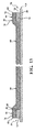
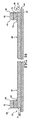
図3,5,6−23に戻って参照すると、第2バスバー58は第1バスバー56から離間しており(spaced from)、グリッドライン部60は第1バスバー56と第2バスバー58との間に配置されている。いくつかの実施形態において、第1バスバー56及び第2バスバー58は互いに反対側であり、グリッドライン部60はそれらの間に配置されている。しかしながら、第1及び第2バスバー56,58は、互いに反対側である必要はないことが明確に理解されるべきである。窓ガラス30が車両の後部窓46である実施形態のような一つの実施形態において、第1バスバー56及び第2バスバー58は基板34上で周囲に配置され、第2バスバー58は第1バスバー56から離間している。窓ガラス30が車両の引窓組立体48用である実施形態のような他の実施形態において、第1バスバー56は基板上で第1側部40に配置され、第2バスバー58は基板34上で第2側部42に配置され、第2バスバー58は第1バスバー56から離間している。特に図9−13を参照すると、様々な実施形態において、第1バスバー56及び第2バスバー58は、基板34上に直接的に配置されている。特に図14−18を参照すると、いくつかの実施形態において、第1バスバー56及び第2バスバー58は、部分的又は完全に基板34のセラミックフリット層44上に配置され、基板34から離間している。特に図19−23を参照すると、他の実施形態において、第1バスバー56及び第2バスバー58は、基板34と、基板34のセラミックフリット層44との間に配置されている。
Referring back to FIGS. 3, 5, 6-23, the
特に図8を参照すると、第3バスバー62を含む実施形態において、第3バスバー62は基板34上に配置されている。第3バスバー62は、典型的に、第1バスバー56と第2バスバー58との間に配置される。第3バスバー62は、基板34の周囲に、基板34の第1側部40に又は基板34の第2側部42に配置されてもよい。一つの実施形態において、第3バスバー62は、基板34の第1側部40に第1バスバー56と共に配置されている。第1バスバー56及び第2バスバー58と同じ様に、第3バスバー62は、部分的又は完全に基板34のセラミックフリット層44上に配置されて、基板34から離間してもよく、又は、基板34と、基板34のセラミックフリット層44との間に配置されてもよい。
With particular reference to FIG. 8, in an embodiment including a third bus bar 62, the third bus bar 62 is disposed on the
図3,5,7,8を参照すると、第1バスバー56及び第2バスバー58は、グリッドライン部60に接する第1エッジ64、及び第1エッジ64の反対側の第2エッジ66をそれぞれ独立して有し、第1エッジ64及び第2エッジ66は、第1エッジ64と第2エッジ66との間にバスバー幅Wを画定する。いくつかの実施形態において、第1バスバー56及び第2バスバー58のうちの少なくとも一つは、12ミリメートル(mm)未満の、代替的に11ミリメートル(mm)未満の、代替的に10ミリメートル(mm)未満の、代替的に9ミリメートル(mm)未満の又は代替的に7ミリメートル(mm)未満のバスバー幅Wを有する。第3バスバー62を含む実施形態において、第3バスバー62は、すぐ上で記述したようなバスバー幅Wを有する。
Referring to FIGS. 3, 5, 7, and 8, the
上述したように、昼光開口部32は、典型的に、セラミックフリット層44によって画定される。このために、昼光開口部32の面積(area)は、セラミックフリット層44によって基板上で規定されてもよい。以下に記述するように、セラミックフリット層44は、典型的にバスバーのバスバー幅Wによって影響される。しかしながら、セラミックフリット層44を含まない実施形態において、昼光開口部32はまた、バスバーのバスバー幅Wによって影響される。換言すれば、昼光開口部32の面積は、バスバー幅Wが最小化される限り、例えセラミックフリット層44が存在しない場合でも、最大化されることができる。典型的に、第1バスバー56及び第2バスバー58のうちの少なくとも一つのバスバー幅Wの減少は、セラミックフリット層44の幅の減少を結果として生じさせ、従って、昼光開口部32の面積の相応の増大を結果として生じさせる。例えば、図3及び5に示される窓ガラス30は、図2及び4に示される従来の窓ガラスと比較して、昼光開口部32の面積が増大している。用語“昼光開口部の面積”は、本明細書において窓ガラス30を参照して用いられる場合、光が基板34を通過することを可能にする基板34の表面積の量を指す。昼光開口部32の面積の増大は、典型的に窓ガラス30の外観の改善及び運転者の感覚/知覚の改善を結果として生じさせる。いくつかの実施形態において、窓ガラス30は、従来の窓ガラスの昼光開口部の面積と比較して、少なくとも1%、代替的に少なくとも2%又は代替的に少なくとも3%の昼光開口部32の面積の増大を有する。そのような割合は低く見えるかも知れないが、関連する産業において、特に昼光開口部32の面積の改善を扱う場合に、これらの割合は有意である。
As described above, the
図1,3,5−8,及び14−24に戻って参照すると、グリッドライン部60は、典型的に、基板34上で昼光開口部32内に配置されている。特に図9−13を参照すると、グリッドライン部60は、基板34上に直接的に配置されてもよい。特に図14−18を参照すると、グリッドライン部60は、基板34のセラミックフリット層44上に部分的に配置されてもよい。特に図19−23を参照すると、グリッドライン部60は、基板34と、基板34のセラミックフリット層44との間に部分的に配置されてもよい。グリッドライン部60は、第1バスバー56に動作的に接続され且つ接する第1端68及び第2バスバー58に動作的に接続され且つ接する第2端70を有する。グリッドライン部60は、電気装置について当技術分野で知られる如何なる形状(configuration)を有してもよい。典型的に、グリッドライン部60は、一つ又はそれ以上の加熱素子72を含み、各加熱素子72は、グリッドライン部60の第1端68からグリッドライン部60の第2端70に延びている。典型的に、複数の加熱素子72は、グリッドライン部60の隣接する加熱素子72の間に一つ又はそれ以上の隙間を画定する。加熱素子72は、直線的な形状、湾曲した形状、クロスハッチ形状、ジグザグ形状、正弦曲線形状又はそれらの組み合わせを有してもよい。様々な実施形態において、グリッドライン部60は、二つ又はそれ以上の加熱素子72を含む。二つ又はそれ以上の加熱素子72が存在しないいくつかの実施形態において、グリッドライン部60には、上述の隙間が無い。
Referring back to FIGS. 1, 3, 5-8, and 14-24, the
グリッドライン長さLは、グリッドライン部60の第1端68及び第2端70の間に画定される。グリッドライン部60は、グリッドライン長さLに沿って基板34の第1表面36上に完全且つ直接的に配置されている。基板34がセラミックフリット層44を有し且つグリッドライン部60がセラミックフリット層44上に部分的に配置されている実施形態において、グリッドライン部60は、グリッドライン長さLに沿って、基板34の第1表面36及びセラミックフリット層44の両方の上に完全且つ直接的に配置されることが、明確に理解されるべきである。
The grid line length L is defined between the
第1バスバー56、第2バスバー58及びグリッドライン部60は、それぞれ独立して導電材料を含む。第1バスバー56、第2バスバー58及びグリッドライン部60の導電材料は、それぞれ独立して抵抗率を有し、それらの抵抗率は、同じであってもよく又は異なっていてもよい。導電材料の抵抗率は、典型的に、電流がそこを通って伝導されたときに熱の発生を結果として生じさせる。この熱の発生は、典型的に、窓ガラス30から結露を除去し、霜を解かすために利用される。いくつかの実施形態において、第1バスバー56及び第2バスバー58の導電材料の抵抗率は、それぞれ独立して、グリッドライン部60の導電材料の抵抗率よりも低い。様々な実施形態において、第1バスバー56又は第2バスバー58の導電材料の抵抗率は、グリッドライン部60の導電材料の抵抗率よりも低い。しかしながら、第1及び第2バスバー24,26の抵抗率は、グリッドライン部60の導電材料の抵抗率よりも低い必要はない。第3バスバー62を含む実施形態において、第3バスバー62はまた、すぐ上で記述したような導電材料を含む。
The
図5及び7−24を参照すると、第1バスバー56、第2バスバー58及びグリッドライン部60は、導電材料の一つ又はそれ以上の層をそれぞれ独立して含む。いくつかの実施形態において、第1及び第2バスバー56,58のうちの少なくとも一つは、導電材料の二つの層を含むか、本質的に導電材料の二つの層から成るか、又は導電材料の二つの層から成る。第3バスバー62を含む実施形態において、第3バスバー62は、導電材料の一つ又はそれ以上の層を含む。いくつかの実施形態において、第3バスバー62は、導電材料の二つの層を含むか、本質的に導電材料の二つの層から成るか、又は導電材料の二つの層から成る。他の実施形態において、第1、第2及び第3バスバー56,58,62のうちの少なくとも一つは、3、4、5、6、7、8、9又は10枚の導電材料の層を含むか、本質的にそれらから成るか、又はそれらから成る。
Referring to FIGS. 5 and 7-24, the
典型的に、導電材料の層の数を増加させることによって、導電材料を含む第1、第2及び第3バスバー56,58,62のうちの少なくとも一つのバスバー幅Wは低減され、一方で、導電材料によって伝導される、従って第1、第2及び第3バスバー56,58,62のうちの少なくとも一つによって伝導される同じ量の電流が維持される。別の言い方をすれば、導電材料の層の数を増加させ、バスバー幅Wを低減することによって、導電材料の断面積は同じままであることができ、それは典型的に第1、第2及び第3バスバー56,58,62のうちの少なくとも一つによって伝導される同じ量の電流を維持する。換言すれば、導電材料の層の数を増加させ、バスバー幅Wを低減することによって、バスバーの電流密度は同じままである。そのため、導電材料の複数の層を含む第1、第2及び第3バスバー56,58,62のうちの少なくとも一つのバスバー幅Wは、典型的に、昼光開口部32の面積の増大を結果として生じさせ、一方で第1、第2及び第3バスバー56,58,62のうちの少なくとも一つによって伝導される同じ量の電流が維持される。セラミックフリット層44を含む実施形態において、バスバー幅Wは、典型的に、セラミックフリット層44の幅の減少、及び昼光開口部32の面積の相応の増大を結果として生じさせ、一方で第1、第2及び第3バスバー56,58,62のうちの少なくとも一つによって伝導される同じ量の電流が維持される。
Typically, by increasing the number of layers of conductive material, at least one bus bar width W of the first, second and third bus bars 56, 58, 62 comprising conductive material is reduced, while The same amount of current conducted by the conductive material and thus conducted by at least one of the first, second and third bus bars 56, 58, 62 is maintained. In other words, by increasing the number of layers of conductive material and reducing the bus bar width W, the cross-sectional area of the conductive material can remain the same, which is typically the first, second and Maintain the same amount of current conducted by at least one of the third bus bars 56, 58, 62. In other words, by increasing the number of layers of conductive material and reducing the bus bar width W, the current density of the bus bar remains the same. Therefore, the width W of at least one of the first, second and third bus bars 56, 58, 62 including multiple layers of conductive material typically results in an increase in the area of the
さらに、導電材料を複数の層に設けることは、バスバー56,58,62における導電材料の厚さを、グリッドライン部60の厚さに対して変化させることを可能にする。そのため、バスバー56,58,62における導電材料の厚さは、グリッドライン部60の厚さよりも大きくてもよい。もしグリッドライン部60が厚くなり過ぎれば、基板34が過剰な熱に起因して損傷し得る。また、グリッドライン部60の厚さが増大するにつれて、エネルギー消費の増大が結果として生じ得る。さらに、導電材料の増加した量の単一の層のみを含むバスバーは、導電材料の複数の層を含む同じ厚さのバスバーと比較して、熱が導電材料を完全に通り抜けて水分を蒸発させることができないことによって引き起こされる不十分な乾燥に起因して、基板から剥離し得る。
Further, providing the conductive material in a plurality of layers enables the thickness of the conductive material in the bus bars 56, 58, 62 to be changed with respect to the thickness of the
第1バスバー56及び第2バスバー58は、基板34上に配置された導電材料の第1層74をそれぞれ独立して含む。いくつかの実施形態において、グリッドライン部60は、基板34上に配置された導電材料の第1層74を含む。更なる実施形態において、第1バスバー56、第2バスバー58及びグリッドライン部60の導電材料の第1層74は、基板34に沿って延びる単一且つ均質な層である。単一且つ均質な層は、その層の中に空所を含み得るが、尚も均質であることが、明確に理解されるべきである。用語“均質(homogenous)”は、本明細書において導電材料を参照して用いられる場合、導電材料の組成を指し、その導電材料を含む第1バスバー56、第2バスバー58及びグリッドライン部60の形状を指さない。第3バスバー62を含む実施形態において、第3バスバー62は導電材料の第1層74を含む。さらに、第3バスバー62を含む実施形態において、第1バスバー56、第2バスバー58、第3バスバー62及びグリッドライン部60の導電材料の第1層74は、上述したように、基板34に沿って延びる単一且つ均質な層であってもよい。
The
第1及び第2バスバー56,58のうちの少なくとも一つは、第1層74上に配置された導電材料の第2層76をそれぞれ独立して含む。いくつかの実施形態において、グリッドライン部60は、基板34上に配置された導電材料の第2層76を含む。第3バスバー62を含む実施形態において、第3バスバー62は導電材料の第2層76を含む。上述したように、いくつかの実施形態において、第1、第2及び第3バスバー56,58,62のうちの少なくとも一つは、追加的な導電材料の層を含む。また上述したように、バスバーのために導電材料の複数の層を利用することによって、バスバーは、低減されたバスバー幅W及びバスバーを通って伝導される得る増大した量の電流を有することができる。第1バスバー56、第2バスバー58、第3バスバー62及びグリッドライン部60のそれぞれのための導電材料の第1層74及び第2層76のそれぞれは、同じであってもよく又は異なっていてもよいことが、明確に理解されるべきである。
At least one of the first and second bus bars 56, 58 independently includes a
いくつかの実施形態において、導電材料の第1層74及び導電材料の第2層76は、20μm以下の、代替的に15μm以下の又は代替的に12μm以下の乾燥膜厚Tをそれぞれ独立して有する。他の実施形態において、導電材料の第1層74及び導電材料の第2層76は、1から20μmの、代替的に3から15μmの又は代替的に6から12μmの乾燥膜厚Tをそれぞれ独立して有する。
In some embodiments, the first layer of
様々な実施形態において、導電材料は、60μm以下の、45μm以下の又は代替的に35μm以下の全乾燥膜厚を有する。更なる実施形態において、導電材料は、1から60μmの、代替的に3から45μmの又は代替的に6から35μmの全乾燥膜厚を有する。 In various embodiments, the conductive material has a total dry film thickness of 60 μm or less, 45 μm or less, or alternatively 35 μm or less. In further embodiments, the conductive material has a total dry film thickness of 1 to 60 μm, alternatively 3 to 45 μm, or alternatively 6 to 35 μm.
導電材料の第1層74及び導電材料の第2層76は、導電材料として銀を含んでもよい。さらに、導電材料は、典型的に銀を含む導電組成物で形成される。しかしながら、導電材料は、特定の形態の炭素(例えば、黒鉛)、銅、金、アルミニウム、亜鉛、真鍮、青銅、導電性酸化物及びそれらの組み合わせ等の他の導電性金属を含んでもよいことが、明確に理解されるべきである。適切な導電性酸化物の例は、インジウムスズ酸化物(ITO)及びフッ素スズ酸化物等の遷移金属酸化物が含まれる。導電材料は、非導電材料を含んでもよく、この窓ガラス30の目的については尚も導電性であり得る。そのような非導電材料の例は、特定の形態の炭素(例えば、カーボンブラック)及びシリカ系酸化物を含むが、それらに限定されない。
The
導電材料は、膜又は被覆(コーティング)の形態で提供されてもよい。典型的には、導電材料は、基板34、セラミックフリット層44又は導電材料の他の層の上に、印刷、刷毛塗り、積層、浸漬、噴霧又は導電材料を配置するための当技術分野で知られる如何なる他の方法を介して配置されてもよい。いくつかの実施形態において、導電材料は、基板34上に印刷された銀ペーストで形成された被覆の形態である。
The conductive material may be provided in the form of a film or a coating. Typically, the conductive material is known in the art for placing printed, brushed, laminated, dipped, sprayed or conductive material on the
いくつかの実施形態において、銀ペーストは、銀、担体(carrier)及び添加剤を含む。銀ペーストはまた、結合剤(binder)を含んでもよい。銀ペーストの担体は、松油(pine oil)を含んでもよい。一つの実施形態において、第1銀ペーストは、1.0から1.4オーム毎フット(Ω/ft)の抵抗率を有する。他の実施形態において、第2銀ペーストは、2.5から4.5Ω/ftの抵抗率を有する。更に他の実施形態において、第3銀ペーストは、4.0から8.0Ω/ftの抵抗率を有する。適切な銀ペーストの市販品の例は、デュポン(登録商標)9903B,デュポン(登録商標)9912B,デュポン(登録商標)9915B,ジョンソン‐マッセイ(登録商標)A6174AP,及びジョンソン‐マッセイ(登録商標)A6175APを含む。デュポン(登録商標)9903Bは、77.8から79.6重量パーセントの銀、40から50Pa‐sの粘度、3.8g/ccの密度、及び1.2Ω/ftの公称抵抗率を有する。デュポン(登録商標)9912は、68.4から70.3重量パーセントの銀、25から35Pa‐sの粘度、3.0g/ccの密度、及び3.9Ω/ftの公称抵抗率を有する。デュポン(登録商標)9915は、57.1から59.1重量パーセントの銀、25から35Pa‐sの粘度、2.2g/ccの密度、及び6.6Ω/ftの公称抵抗率を有する。ジョンソン‐マッセイ(登録商標)A6174APは、77.0から79.0重量パーセントの銀、25から30Pa‐sの粘度、3.76g/ccの密度、及び0.85Ω/ftの公称抵抗率を有する。ジョンソン‐マッセイ(登録商標)A6175APは、63.5から65.5重量パーセントの銀、25から30Pa‐sの粘度、2.55g/ccの密度、及び2.0Ω/ftの公称抵抗率を有する。 In some embodiments, the silver paste includes silver, a carrier and an additive. The silver paste may also contain a binder. The silver paste carrier may include pine oil. In one embodiment, the first silver paste has a resistivity of 1.0 to 1.4 ohm per foot (Ω / ft). In other embodiments, the second silver paste has a resistivity of 2.5 to 4.5 Ω / ft. In yet another embodiment, the third silver paste has a resistivity of 4.0 to 8.0 Ω / ft. Examples of suitable silver paste products are DuPont® 9903B, DuPont® 9912B, DuPont® 9915B, Johnson-Massey® A6174AP, and Johnson-Massey® A6175AP. including. DuPont® 9903B has 77.8 to 79.6 weight percent silver, a viscosity of 40 to 50 Pa-s, a density of 3.8 g / cc, and a nominal resistivity of 1.2 Ω / ft. DuPont® 9912 has 68.4 to 70.3 weight percent silver, a viscosity of 25 to 35 Pa-s, a density of 3.0 g / cc, and a nominal resistivity of 3.9 Ω / ft. DuPont® 9915 has 57.1 to 59.1 weight percent silver, a viscosity of 25 to 35 Pa-s, a density of 2.2 g / cc, and a nominal resistivity of 6.6 Ω / ft. Johnson-Massey® A6174AP has 77.0 to 79.0 weight percent silver, a viscosity of 25 to 30 Pa-s, a density of 3.76 g / cc, and a nominal resistivity of 0.85 Ω / ft . Johnson-Massey® A6175AP has 63.5 to 65.5 weight percent silver, a viscosity of 25 to 30 Pa-s, a density of 2.55 g / cc, and a nominal resistivity of 2.0 Ω / ft .
いくつかの実施形態において、第1銀ペーストは、それぞれ100重量部の第1銀ペーストに基づいて、45から75重量部、代替的に50から70重量部又は代替的に55から65重量部の量のデュポン(登録商標)9903B、及び、25から55重量部、代替的に30から50重量部又は代替的に35から45重量部の量のデュポン(登録商標)9912B、を含んでもよい。様々な実施形態において、第2銀ペーストは、それぞれ100重量部の第1銀ペーストに基づいて、70から100重量部、代替的に75から100重量部又は代替的に80から100重量部の量のデュポン(登録商標)9903B、及び、0から30重量部、代替的に0から25重量部又は代替的に0から20重量部の量のデュポン(登録商標)9912B、を含んでもよい。 In some embodiments, the first silver paste is 45 to 75 parts by weight, alternatively 50 to 70 parts by weight, or alternatively 55 to 65 parts by weight, each based on 100 parts by weight of the first silver paste. An amount of DuPont® 9903B and DuPont® 9912B in an amount of 25 to 55 parts by weight, alternatively 30 to 50 parts by weight, or alternatively 35 to 45 parts by weight may be included. In various embodiments, the second silver paste is in an amount of 70 to 100 parts by weight, alternatively 75 to 100 parts by weight, or alternatively 80 to 100 parts by weight, each based on 100 parts by weight of the first silver paste. And DuPont (R) 9903B, and DuPont (R) 9912B in an amount of 0 to 30 parts by weight, alternatively 0 to 25 parts by weight, or alternatively 0 to 20 parts by weight.
導電材料が銀ペーストで形成される実施形態において、銀ペーストの成分は、複数の層を有する導電材料の層間剥離(delamination)を結果として生じさせ得る。より具体的には、銀ペーストが松油を含む実施形態において、松油は、基板34、セラミックフリット層44又は導電材料の他の層からの導電材料の層間剥離を引き起こし得る。以下により詳細に記述するように、この層間剥離は、導電材料の追加的な層を配置するより前に導電材料の各層を乾燥させることによって、最小化されることができる。いくつかの実施形態において、層間剥離の危険性を最小化するために、導電材料の各層は20μm以下の乾燥膜厚Tを有し、導電材料は60μm以下の全乾燥膜厚を有する。
In embodiments where the conductive material is formed of a silver paste, the components of the silver paste can result in delamination of the conductive material having multiple layers. More specifically, in embodiments where the silver paste includes pine oil, the pine oil may cause delamination of the conductive material from the
特に図24を参照すると、導電材料の各層をその上に配置するより前に、メッシュスクリーンを基板34上に(また、利用される場合、導電材料の(複数の)層上に)配置してもよい。第1メッシュスクリーン78は、孔を含み、40から100本/インチ、代替的に50から90本/インチ、又は代替的に60から80本/インチの孔サイズ数を有する。第2メッシュスクリーン80は、孔を含み、130から250本/インチ、代替的に180から220本/インチ、又は代替的に190から210本/インチの孔サイズ数を有する。典型的に、メッシュスクリーンの孔サイズは、導電材料に由来する熱の発生に影響を及ぼす。そのため、メッシュスクリーンの孔のサイズの増大(すなわち、孔サイズ数の減少)は、導電材料の熱の発生を増大させ、逆もまた同様である。メッシュスクリーンは導電組成物の配置の後に導電材料の層と共に配置されてもよいことが、明確に理解されるべきである。
Referring specifically to FIG. 24, prior to placing each layer of conductive material thereon, a mesh screen is placed on substrate 34 (and, if utilized, on the layer (s) of conductive material). Also good. The
特に図10,12,15,17,20及び22を参照すると、いくつかの実施形態において、導電材料の第1層74は第1銀ペーストで形成され、第1層74は第1の抵抗率を有しており、また導電材料の第2層76は第2銀ペーストで形成され、第2層76は、第1の抵抗率よりも低い第2の抵抗率を有している。そのため、第1層74及び第2層76の導電材料は、異なっている。そのため、これらの実施形態において、第1バスバー56、第2バスバー58及びグリッドライン部60のそれぞれの導電材料の第1層74は、第1の抵抗率(すなわち、より高い抵抗率)を有しており、第1バスバー56及び第2バスバー58のそれぞれの導電材料の第2層76は、第2の抵抗率(すなわち、より低い抵抗率)を有している。このために、また第1層74の抵抗率に比べて低い導電材料の第2層76の抵抗率に起因して、第1バスバー56及び第2バスバー58のそれぞれの導電材料は、グリッドライン部60の導電材料の抵抗率よりも低い抵抗率を有する。いくつかの実施形態において、導電材料の第1層74は2.4から5.1Ω‐ftの抵抗率を有し、導電材料の第2層76は1.0から3.9Ω‐ftの抵抗率を有し、導電材料の第1層74の抵抗率は導電材料の第2層76の抵抗率よりも大きい。第3バスバー62を含む実施形態において、第3バスバー62は、すぐ上で記述したような、第1層74及び第2層76を含んでもよい。
With particular reference to FIGS. 10, 12, 15, 17, 20, and 22, in some embodiments, the
特に図9,11,14,16,19及び21を参照すると、様々な実施形態において、導電材料の第1層74及び第2層76の両方は第2銀ペーストで形成され、第2の抵抗率を有する。そのため、第1層74及び第2層76の導電材料は、同じである。そのため、これらの実施形態において、第1バスバー56、第2バスバー58及びグリッドライン部60のそれぞれの導電材料の第1層74は、第2の抵抗率を有しており、第1バスバー56及び第2バスバー58のそれぞれの導電材料の第2層76もまた、第2の抵抗率を有している。グリッドライン部60のより低い抵抗率を有するこれらの実施形態は、より小さな表面積を有する窓ガラス30用に利用されてもよい。なぜなら、より少ない熱の発生が、この窓ガラス30から結露を除去し、霜を解かすために要求されるからである。いくつかの実施形態において、導電材料の第1層74及び導電材料の第2層76は、1.0から3.9Ω‐ftの抵抗率をそれぞれ独立して有する。第3バスバー62を含む実施形態において、第3バスバー62は、すぐ上で記述したような、第1層74及び第2層76を含んでもよい。
With particular reference to FIGS. 9, 11, 14, 16, 19 and 21, in various embodiments, both the
特に図13,18及び23を参照して、他の実施形態において、導電材料の第1層74は第2銀ペーストで形成され、第1層74は第2の抵抗率を有しており、また導電材料の第2層76は第1銀ペーストで形成され、第2層76は、第2の抵抗率よりも高い第1の抵抗率を有している。そのため、第1層74及び第2層76の導電材料は、異なっている。そのため、これらの実施形態において、第1バスバー56、第2バスバー58のそれぞれの導電材料の第1層74は、第2の抵抗率(すなわち、より低い抵抗率)を有しており、第1バスバー56、第2バスバー58及びグリッドライン部60のそれぞれの導電材料の第2層76は、第1の抵抗率(すなわち、より高い抵抗率)を有している。このために、また第1層74の抵抗率に比べて高い導電材料の第2層76の抵抗率に起因して、第1バスバー56及び第2バスバー58のそれぞれの導電材料は、グリッドライン部60の導電材料の抵抗率よりも低い抵抗率を有する。いくつかの実施形態において、導電材料の第1層74は1.0から3.9Ω‐ftの抵抗率を有し、導電材料の第2層76は2.4から5.1Ω‐ftの抵抗率を有し、導電材料の第2層76の抵抗率は導電材料の第1層74の抵抗率よりも大きい。第3バスバー62を含む実施形態において、第3バスバー62は、すぐ上で記述したような、第1層74及び第2層76を含んでもよい。
With particular reference to FIGS. 13, 18 and 23, in another embodiment, the
上述したセラミックフリット層44に戻って参照すると、セラミックフリット層44は、セラミック及び少なくとも一つの担体を含むセラミック組成物で形成されてもよい。適切なセラミック組成物の例は、フェロ(登録商標)AD3402Aを含む。フェロ(登録商標)AD3402Aは、ビスマス、ニッケル鉄クロマイト、銅クロマイト、石英ケイ酸塩、シリコン及び溶剤を含む。セラミックフリット層44は、基板34とは別個の層として別個のステップで基板34に適用されてもよく、又は、基板34は、もともと既にその上に一体的されたセラミックフリット層44を有して設けられてもよいことが、明確に理解されるべきである。セラミック組成物の担体は、松油を含んでもよい。セラミック組成物の担体が松油を含む実施形態において、松油は、基板34からの導電材料の層間剥離を引き起こし得る。以下により詳細に記述するように、この層間剥離は、その上に導電材料を配置するより前に、セラミック組成物で形成されたセラミックフリット層44を乾燥させることによって、最小化されることができる。
Referring back to the
特に図5,7及び8を参照すると、窓ガラス30はまた、電気装置86に動作的に接続され且つ電気的に通じているリード線を含んでもよい。より具体的には、いくつかの実施形態において、第1リード線86は第1バスバー56に動作的に接続され且つ電気的に通じており、第2リード線88は第2バスバー58に動作的に接続され且つ電気的に通じている。第1リード線86(又は代替的に第2リード線88)は、典型的に、上述したエネルギー源に動作的に接続され且つ電気的に通じている。第2リード線88(又は代替的に第1リード線86)は、典型的に、同様に上述したように、車両のグラウンドに動作的に接続され且つ電気的に通じている。第3バスバー62を含む実施形態において、第1リード線86又は第2リード線88は、第3バスバー62に動作的に接続され且つ電気的に通じてもよい。第1バスバー56及び第3バスバー62が両方とも基板34の第1側部40に配置されている実施形態において、第1リード線86又は第2リード線88は第1バスバー56に動作的に接続され且つ電気的に通じてもよく、第1リード線86又は第2リード線88のうちの他方は第3バスバー62に動作的に接続され且つ電気的に通じてもよい。そのため、両方のリード線86,88は、基板34の第1側部40に隣接して配置される。
With particular reference to FIGS. 5, 7 and 8, the
いくつかの実施形態において、導電材料は、導電材料の第1層74と導電材料の第2層76との間にはんだが無い(free of solder)。導電材料上に配置されたはんだ接合(solder joints)を含む導電材料は、尚も導電材料の第1層74と導電材料の第2層76との間にはんだが無いことが、明確に理解されるべきである。
In some embodiments, the conductive material is free of solder between the
いくつかの実施形態において、電気装置54は、二つ以下のはんだ接合を含む。典型的に、二つのはんだ接合を含む実施形態において、はんだ接合のうちの一つは第1リード線54を電気装置54に動作的に接続し、他方のはんだ接合は第2リード線56を電気装置54に動作的に接続する。換言すれば、電気装置54は、第1リード線86及び第2リード線88を電気装置54に動作的に接続するはんだ接合以外のはんだ接合を全く有さなくてもよい。
In some embodiments,
様々な実施形態において、電気装置54には、導電編組が無い。導電編組は、はんだ付け不良の発生に起因する歩留まり低下、及び、追加的なはんだ接合の使用に起因する生産時間及び費用の増加を、結果として生じさせ得る。
In various embodiments, the
本開示はまた、窓ガラス30を形成するための方法に関する。上述したように、電気装置54は、第1バスバー56、第2バスバー58及びグリッドライン部60を含み、第1バスバー56、第2バスバー58及びグリッドライン部60は、互いに電気的に通じており、導電材料をそれぞれ独立して含む。いくつかの実施形態において、第1及び第2バスバー56,58は、基板34及びセラミックフリット層44のうちの少なくとも一つの上に配置されており、グリッドライン部60は、基板34及びセラミックフリット層44のうちの少なくとも一つの上に配置されている。様々な実施形態において、上述したように、電気装置54は、第1メッシュスクリーン78及び第2メッシュスクリーン80を更に含む。
The present disclosure also relates to a method for forming the
図1,3及び5−24に戻って参照すると、窓ガラス30を形成する方法は、基板34を提供するステップを含む。方法は、基板34がセラミックフリット層44を有するように、基板34上にセラミック組成物を供給及び配置し、基板34上にセラミックフリット層44を形成するステップを更に含んでもよい。いくつかの実施形態において、基板34がセラミックフリット層44を基板34の周囲(periphery)に有し、昼光開口部32を画定するように、セラミック組成物は、基板34の周囲に配置されている。他の実施形態において、基板34がセラミックフリット層44を基板34の第1側部40及び基板34の第2側部42に有し、基板の第1側部40と第2側部42との間に昼光開口部を画定するように、セラミック組成物は、基板34の第1側部40及び基板34の第2側部42に配置されている。
Referring back to FIGS. 1, 3, and 5-24, the method of forming the
方法は、基板34上に第1導電組成物を供給及び配置し、第1バスバー56及び第2バスバー58の導電材料の第1層74を形成するステップを更に含む。いくつかの実施形態において、グリッドライン部60は、基板34上に配置され、第1導電組成物を配置するステップで形成される。そのため、第1導電組成物を供給及び配置するステップは、第1導電組成物を基板34上に供給及び配置して、第1バスバー56、第2バスバー58及びグリッドライン部60の導電材料の第1層74を形成するステップとして、更に規定される。第3バスバー62を含む実施形態において、第1導電組成物を基板34上に配置するステップは、第3バスバー62の導電材料の第1層74を更に形成する。いくつかの実施形態において、第1導電組成物が少なくとも基板34のセラミックフリット層44の上に配置されるように、基板上にセラミック組成物を配置するステップは、第1導電組成物を配置するステップより前に行われる。いくつかの実施形態において、第1導電組成物は、第1銀ペーストとして更に規定される。
The method further includes supplying and placing a first conductive composition on the
方法は、第1バスバー56及び第2バスバー58のうちの少なくとも一つの導電材料の第1層74上に第2導電組成物を供給及び配置し、第1バスバー56及び第2バスバー58のうちの少なくとも一つの導電材料の第2層76を形成するステップを更に含む。いくつかの実施形態において、グリッドライン部60は、基板34上に配置され、第2導電組成物を配置するステップで形成される。そのため、第2導電組成物を供給及び配置するステップは、基板34及び第1バスバー56及び第2バスバー58のうちの少なくとも一つの導電材料の第1層74上第2導電組成物を供給及び配置し、グリッドライン部60及び第1バスバー56及び第2バスバー58のうちの少なくとも一つの導電材料の第2層76を形成するステップとして更に規定される。第3バスバー62を含む実施形態において、導電材料の第1層74上に第2導電組成物を配置するステップは、第3バスバー62の導電材料の第2層76を更に形成する。いくつかの実施形態において、セラミックフリット層44が少なくとも導電材料の上に配置されるように、セラミック組成物を配置するステップは、第2導電組成物を配置するステップより後に行われる。いくつかの実施形態において、第2導電組成物は、第2銀ペーストとして更に規定される。
The method supplies and places a second conductive composition on a
第2導電組成物は、第1導電組成物と同じであるか又は異なっている。いくつかの実施形態において、第1導電組成物は第1銀ペーストとして更に規定され、第2導電組成物は第2銀ペーストとして更に規定される。他の実施形態において、第1導電組成物及び第2導電組成物は第2銀ペーストとして更に規定される。 The second conductive composition is the same as or different from the first conductive composition. In some embodiments, the first conductive composition is further defined as a first silver paste and the second conductive composition is further defined as a second silver paste. In other embodiments, the first conductive composition and the second conductive composition are further defined as a second silver paste.
いくつかの実施形態において、第1導電組成物を配置するステップ及び第2導電組成物を配置するステップは、第1導電組成物を印刷するステップ及び第2導電組成物を印刷するステップとして更に規定される。 In some embodiments, placing the first conductive composition and placing the second conductive composition are further defined as printing the first conductive composition and printing the second conductive composition. Is done.
方法は、基板上に第1導電組成物を配置するステップより前に、セラミックフリット層44に熱を加えるステップを更に含んでもよい。いくつかの実施形態において、熱を加えるステップは、赤外線ランプ又は伝導加熱(conductive heating)を用いて行われる。熱を加えるステップは、乾燥ステップとも呼ばれる。セラミックフリット層44に熱を加えるステップは、典型的に、華氏300から450度の温度で実行される。セラミックフリット層44のための乾燥時間は、典型的に30秒と90秒の間である。
The method may further include applying heat to the
方法は、第1バスバー56及び第2バスバー58のうちの少なくとも一つの導電材料の第1層74上に第2導電組成物を配置するステップより前に、導電材料の第1層74に熱を加えるステップを更に含んでもよい。導電材料の第1層74に熱を加えるステップは、典型的に、華氏300から500度の温度で実行される。導電材料の第1層74のための乾燥時間は、典型的に30秒と120秒の間である。
The method applies heat to the
方法は、導電材料の第2層76に熱を加えるステップを更に含んでもよい。導電材料の第2層76に熱を加えるステップは、典型的に、華氏300から500度の温度で実行される。導電材料の第2層76のための乾燥時間は、典型的に30秒と120秒の間である。
The method may further include applying heat to the
様々な実施形態において、セラミックフリット層44、導電材料の第1層74及び導電材料の第2層76を乾燥するステップは、基板34若しくはセラミックフリット層44からの導電材料の層間剥離又は導電材料の他の層からの導電材料の一つの層の層間剥離の危険性を最小化する。
In various embodiments, the step of drying the
方法は、基板34上に第1導電組成物を配置するステップより前に、基板34上に第1メッシュスクリーン78を配置するステップを更に含んでもよい。そのため、基板34上に第1導電組成物を配置するステップは、基板34、第1メッシュスクリーン78又はそれらの組み合わせの上に第1導電組成物を配置するステップとして更に規定される。
The method may further include disposing a
方法は、導電材料の第1層74上に第2導電組成物を配置するステップより前に、導電材料の第1層74上に第2メッシュスクリーン80を配置するステップを更に含んでもよい。そのため、導電材料の第1層74上に第2導電組成物を配置するステップは、導電材料の第1層74、第2メッシュスクリーン80又はそれらの組み合わせの上に第2導電組成物を配置するステップとして更に規定される。
The method may further include disposing a
窓ガラス30を形成する方法の幾つかの実施形態の非限定的な例が、以下に記述される。特に図15を参照すると、窓ガラス30の一つの実施形態において、方法は、基板34及びセラミックフリット層44のうちの少なくとも一つの上に第1銀ペーストを供給及び配置し、グリッドライン部60並びに第1及び第2バスバー56,58のそれぞれの導電材料の第1層74を形成するステップを更に含む。本実施形態の方法は、第1層74を乾燥させるステップを更に含む。本実施形態の方法は、第1層74上に第2銀ペーストを供給及び配置して、第1及び第2バスバー56,58のうちの少なくとも一つの導電材料の第2層76を形成するステップを更に含む。本実施形態の方法は、第2層76を乾燥させるステップを更に含む。本実施形態において、乾燥ステップは、赤外線ランプ又は伝導熱(conductive heat)を用いて行われる。
Non-limiting examples of some embodiments of the method of forming the
特に図15及び24を参照すると、他の実施形態において、方法は、第1及び第2バスバー56,58のうちの少なくとも一つについて、基板34及びセラミックフリット20のうちの少なくとも一つの上に第1メッシュスクリーン78を提供及び配置するステップを更に含む。本実施形態の方法は、基板34、セラミックフリット層44及び第1メッシュスクリーン78のうちの少なくとも一つの上に第1銀ペーストを供給及び配置し、グリッドライン部60並びに第1及び第2バスバー56,58のそれぞれの導電材料の第1層74を形成するステップを更に含む。本実施形態の方法は、第1層74を乾燥させるステップを更に含む。本実施形態の方法は、第1及び第2バスバー56,58のうちの少なくとも一つの導電材料の第1層74上に第2メッシュスクリーン80を提供及び配置するステップを更に含む。本実施形態の方法は、第1層74及び第2メッシュスクリーン80の少なくとも一つの上に第2銀ペーストを供給及び配置して、第1及び第2バスバー56,58のうちの少なくとも一つの導電材料の第2層76を形成するステップを更に含む。本実施形態の方法は、第2層76を乾燥させるステップを更に含む。本実施形態において、乾燥ステップは、赤外線ランプ又は伝導熱を用いて行われる。
With particular reference to FIGS. 15 and 24, in another embodiment, the method includes, for at least one of the first and second bus bars 56, 58, on the at least one of the
特に図14を参照すると、他の実施形態において、方法は、基板34及びセラミックフリット層44のうちの少なくとも一つの上に第2銀ペーストを供給及び配置し、グリッドライン部60並びに第1及び第2バスバー56,58のそれぞれの導電材料の第1層74を形成するステップを更に含む。本実施形態の方法は、第1層74を乾燥させるステップを更に含む。本実施形態の方法は、第1層74上に第2銀ペーストを供給及び配置して、第1及び第2バスバー56,58のうちの少なくとも一つの導電材料の第2層76を形成するステップを更に含む。本実施形態の方法は、第2層76を乾燥させるステップを更に含む。本実施形態において、乾燥ステップは、赤外線ランプ又は伝導熱を用いて行われる。
Referring specifically to FIG. 14, in another embodiment, the method supplies and places a second silver paste on at least one of the
特に図14及び24を参照すると、他の実施形態において、方法は、第1及び第2バスバー56,58のうちの少なくとも一つについて、基板34及びセラミックフリット層44のうちの少なくとも一つの上に第2メッシュスクリーン78を提供及び配置するステップを更に含む。本実施形態の方法は、基板34、セラミックフリット層44及び第2メッシュスクリーン80のうちの少なくとも一つの上に第2銀ペーストを供給及び配置し、グリッドライン部60並びに第1及び第2バスバー56,58のそれぞれの導電材料の第1層74を形成するステップを更に含む。本実施形態の方法は、第1層74を乾燥させるステップを更に含む。本実施形態の方法は、第1及び第2バスバー56,58のうちの少なくとも一つの導電材料の第1層74上に第2メッシュスクリーン80を提供及び配置するステップを更に含む。本実施形態の方法は、第1層74及び第2メッシュスクリーン80の少なくとも一つの上に第2銀ペーストを供給及び配置して、第1及び第2バスバー56,58のうちの少なくとも一つの導電材料の第2層76を形成するステップを更に含む。本実施形態の方法は、第2層76を乾燥させるステップを更に含む。本実施形態において、乾燥ステップは、赤外線ランプ又は伝導熱を用いて行われる。
With particular reference to FIGS. 14 and 24, in another embodiment, the method includes, on at least one of the first and second bus bars 56, 58, on at least one of the
添付の特許請求の範囲は、詳細な説明において明示的に記述された明示的及び特定の化合物、組成物又は方法に限定されず、添付の特許請求の範囲に含まれる特定の実施形態の間で変更することができることが、理解されるべきである。様々な実施形態の特定の特徴又は態様を記述することについて本明細書に依存する如何なるマーカッシュグループに関しても、他の全てのマーカッシュメンバーから独立して、それぞれのマーカッシュグループの各メンバーから、異なる、特別な及び/又は予想外の結果が獲得され得ることが、明確に理解されるべきである。マーカッシュグループの各メンバーは、個別に又は組み合わせて依存されることができ、添付の特許請求の範囲内の特定の実施形態に対する適切なサポートを提供する。 The appended claims are not limited to the explicit and specific compounds, compositions, or methods expressly set forth in the detailed description, but between the specific embodiments encompassed by the appended claims. It should be understood that changes can be made. For any Markush group that relies on this specification for describing specific features or aspects of the various embodiments, each member of the respective Markush group is distinct from each other member of the Markush group, independently of any other Markush group. It should be clearly understood that no and / or unexpected results can be obtained. Each member of the Markush group can be relied upon individually or in combination to provide appropriate support for specific embodiments within the scope of the appended claims.
本開示の様々な実施形態を記述することにおいて依存される任意の範囲及び部分範囲は、独立して及び集合的に添付の特許請求の範囲内に含まれ、たとえそのような値が本明細書において明示的に記載されていなくても、その中の全体の値及び/又は小部分の(fractional)値を含む全ての範囲を記述及び企図すると理解されることもまた、理解されるべきである。当業者は、列挙された範囲及び部分範囲(subrange)は本開示の様々な実施形態を十分に記述し且つ可能にし、そのような範囲及び部分的な範囲は関連する半分、三分の一、四分の一、五分の一等に更に線引きされてもよいことを、容易に認識する。ほんの一例として、“0.1から0.9”の範囲は、下の三分の一、すなわち、0.1から0.3に、中央の三分の一、すなわち0.4から0.6に、及び上の三分の一、すなわち0.7から0.9に更に線引きされてもよい。それらは、個別に及び集合的に添付の特許請求の範囲内であり且つ個別に及び/又は集合的に依存されることができ、添付の特許請求の範囲内の特定の実施形態に対する適切なサポートを提供する。加えて、“少なくとも”、“より大きい”、“より小さい”、“以下”等のような、範囲を規定又は修飾する言語に関して、そのような言語は、部分範囲及び/又は上限若しくは下限を含むことが理解されるべきである。他の例として、“少なくとも10”の範囲は、本来、少なくとも10から35の部分範囲、少なくとも10から25の部分範囲、少なくとも25から35の部分範囲等を含み、各部分範囲は、個別に及び/又は集合的に依存されることができ、添付の特許請求の範囲内の特定の実施形態に対する適切なサポートを提供する。最後に、開示された範囲内の個別の数字は、依存されることができ、添付の特許請求の範囲内の特定の実施形態に対する適切なサポートを提供する。例えば、“1から9”の範囲は、様々な個別の整数、例えば3、並びに小数点を含む個別の数字(又は分数)、例えば4.1、を含む。それらは、依存されることができ、添付の特許請求の範囲内の特定の実施形態に対する適切なサポートを提供する。 Any ranges and subranges relied upon in describing various embodiments of the present disclosure are included, independently and collectively, within the scope of the appended claims, even if such values are It is also to be understood that the entire range and / or fractional values therein are described and contemplated, even if not explicitly stated in . Those skilled in the art will appreciate that the listed ranges and subranges fully describe and enable various embodiments of the present disclosure, such ranges and subranges being related half, one third, Recognize easily that it may be further drawn to a quarter, a fifth, etc. By way of example only, the range of “0.1 to 0.9” is the lower third, ie 0.1 to 0.3, and the middle third, ie 0.4 to 0.6. And may be further drawn to the upper third, ie 0.7 to 0.9. They are individually and collectively within the scope of the appended claims and can be individually and / or collectively dependent upon, with appropriate support for specific embodiments within the scope of the appended claims. I will provide a. In addition, for languages that define or modify ranges, such as “at least”, “greater than”, “less than”, “less than”, etc., such languages include subranges and / or upper or lower limits It should be understood. As another example, a range of “at least 10” inherently includes at least 10 to 35 subranges, at least 10 to 25 subranges, at least 25 to 35 subranges, etc., each subrange individually and It may be / or may be collectively relied upon to provide appropriate support for specific embodiments within the scope of the appended claims. Finally, individual numbers within the disclosed scope can be relied upon and provide appropriate support for specific embodiments within the scope of the appended claims. For example, the range “1 to 9” includes various individual integers such as 3, as well as individual numbers (or fractions) including a decimal point, such as 4.1. They can be relied upon and provide adequate support for specific embodiments within the scope of the appended claims.
本開示は、例示的な方法で本明細書において記述されており、使用された用語は、限定ではなく記述の語の本質であるように意図されていることが、理解されるべきである。上記の教示に照らして、本開示の多くの変更及び変形が可能である。本開示は、添付の特許請求の範囲内で、具体的に記述されたものと異なる方法で実施され得る。独立請求項並びに単一従属及び多数従属の両方の従属請求項の全ての組み合わせの目的物は、本明細書において明示的に企図されている。
It is to be understood that this disclosure is described herein in an illustrative manner, and that the terminology used is intended to be the essence of the terminology described rather than limitation. Many modifications and variations of the present disclosure are possible in light of the above teachings. The present disclosure may be practiced otherwise than as specifically described within the scope of the appended claims. The objects of independent claims and all combinations of single and multiple dependent claims are expressly contemplated herein.
Claims (39)
第1表面及び該第1表面の反対側の第2表面を有する基板、及び
第1バスバー、第2バスバー及びグリッドライン部を有する電気装置であり、前記第1バスバー、前記第2バスバー及び前記グリッドライン部は、互いに電気的に通じており、導電材料をそれぞれ独立して有する、電気装置、
を有し、
前記第1バスバーは前記基板上に配置され、前記第2バスバーは前記第1バスバーから離間して前記基板上に配置され、前記グリッドライン部は、前記第1バスバーに動作的に接続され且つ接する第1端及び前記第2バスバーに動作的に接続され且つ接する第2端を有し、グリッドライン長さは、前記グリッドライン部の前記第1端及び前記第2端の間に画定され、前記グリッドライン部は、前記グリッドライン長さに沿って前記基板の前記第1表面上に完全且つ直接的に配置され、
前記第1バスバー及び前記第2バスバーは、前記基板上に配置された前記導電材料の第1層をそれぞれ独立して有し、前記第1バスバー及び前記第2バスバーのうちの少なくとも一つは、前記第1層上に配置された前記導電材料の第2層をそれぞれ独立して有し、
前記グリッドライン部は、前記導電材料の前記第1層又は前記導電材料の前記第2層の一つを有し、
前記第1層及び前記第2層の前記導電材料は、同じであるか又は異なっている、
窓ガラス。 A window glass having a daylight opening,
A substrate having a first surface and a second surface opposite to the first surface, and an electric device having a first bus bar, a second bus bar, and a grid line portion, the first bus bar, the second bus bar, and the grid The line portions are in electrical communication with each other and each have an electrically conductive material independently;
Have
The first bus bar is disposed on the substrate, the second bus bar is disposed on the substrate so as to be separated from the first bus bar, and the grid line portion is operatively connected to and in contact with the first bus bar. A first end and a second end operatively connected to and in contact with the second bus bar, a grid line length being defined between the first end and the second end of the grid line portion; A grid line portion is disposed completely and directly on the first surface of the substrate along the grid line length;
The first bus bar and the second bus bar each independently have a first layer of the conductive material disposed on the substrate, and at least one of the first bus bar and the second bus bar is: Each independently having a second layer of the conductive material disposed on the first layer;
The grid line portion has one of the first layer of the conductive material or the second layer of the conductive material,
The conductive materials of the first layer and the second layer are the same or different;
Window glass.
基板を提供するステップ、
基板上に第1導電組成物を配置し、前記第1バスバー及び前記第2バスバーの前記導電材料の第1層を形成するステップ、及び
前記第1バスバー及び前記第2バスバーのうちの少なくとも一つの前記導電材料の第1層上に、第1導電組成物と同じであるか又は異なっている、第2導電組成物を配置し、前記第1バスバー及び前記第2バスバーのうちの少なくとも一つの前記導電材料の第2層を形成するステップ、
を含み、
前記グリッドライン部は、前記基板上に配置され、前記第1導電組成物を配置する前記のステップで形成されるか又は前記第2導電組成物を配置する前記のステップで形成される、
方法。 A method for forming a window glass having a daylight opening, wherein the window glass includes an electric device having a first bus bar, a second bus bar, and a grid line portion, and the first bus bar, the second bus bar, and the second bus bar. The bus bar and the grid line portion each have a conductive material independently and are in electrical communication with each other.
Providing a substrate;
Disposing a first conductive composition on a substrate to form a first layer of the conductive material of the first bus bar and the second bus bar; and at least one of the first bus bar and the second bus bar. A second conductive composition is disposed on the first layer of the conductive material, the second conductive composition being the same as or different from the first conductive composition, and at least one of the first bus bar and the second bus bar. Forming a second layer of conductive material;
Including
The grid line portion is disposed on the substrate and formed in the step of disposing the first conductive composition or formed in the step of disposing the second conductive composition.
Method.
The method according to any one of claims 24 to 38, wherein the first layer of the conductive material and the second layer of the conductive material each independently have a dry film thickness of 20 µm or less.
Applications Claiming Priority (3)
| Application Number | Priority Date | Filing Date | Title |
|---|---|---|---|
| US201461986534P | 2014-04-30 | 2014-04-30 | |
| US61/986,534 | 2014-04-30 | ||
| PCT/US2015/028656 WO2015168476A1 (en) | 2014-04-30 | 2015-04-30 | Busbar for an electrical device and a window pane including the same |
Publications (1)
| Publication Number | Publication Date |
|---|---|
| JP2017520083A true JP2017520083A (en) | 2017-07-20 |
Family
ID=53189194
Family Applications (1)
| Application Number | Title | Priority Date | Filing Date |
|---|---|---|---|
| JP2016565177A Pending JP2017520083A (en) | 2014-04-30 | 2015-04-30 | Bus bar for electric device and window glass including the same |
Country Status (4)
| Country | Link |
|---|---|
| US (1) | US20150314757A1 (en) |
| EP (1) | EP3138364A1 (en) |
| JP (1) | JP2017520083A (en) |
| WO (1) | WO2015168476A1 (en) |
Cited By (1)
| Publication number | Priority date | Publication date | Assignee | Title |
|---|---|---|---|---|
| JP2019077571A (en) * | 2017-10-20 | 2019-05-23 | Agc株式会社 | Glass laminate for vehicle |
Families Citing this family (3)
| Publication number | Priority date | Publication date | Assignee | Title |
|---|---|---|---|---|
| US10843644B2 (en) * | 2016-09-16 | 2020-11-24 | Magna Mirrors Of America, Inc. | Vehicle liftgate window assembly with heater grid |
| US11234297B2 (en) * | 2018-02-26 | 2022-01-25 | Charmgraphene Co., Ltd. | Plate heater |
| DE102020200561A1 (en) | 2020-01-17 | 2021-07-22 | Volkswagen Aktiengesellschaft | Laminated window for a motor vehicle, head-up display |
Citations (8)
| Publication number | Priority date | Publication date | Assignee | Title |
|---|---|---|---|---|
| JPS547414A (en) * | 1977-06-17 | 1979-01-20 | Nippon Sheet Glass Co Ltd | Method and apparatus for printing conductive frit paste on substrate |
| GB2223385A (en) * | 1988-06-22 | 1990-04-04 | Splintex Belge Sa | Vitreous substrate bearing electric circuit components and method of manufacturing same |
| JPH0634341Y2 (en) * | 1987-07-20 | 1994-09-07 | 日本板硝子株式会社 | Laminated structure of ceramic color layer and conductive layer |
| JPH06318492A (en) * | 1989-10-09 | 1994-11-15 | Asahi Glass Co Ltd | Electric heater glass |
| JPH11208421A (en) * | 1998-01-28 | 1999-08-03 | Asahi Glass Co Ltd | Defogging glass for automobile |
| JP2006202723A (en) * | 2004-11-12 | 2006-08-03 | Agc Automotive Americas R & D Inc | Electric connector for glass door of vehicle |
| US20120291353A1 (en) * | 2011-05-20 | 2012-11-22 | Dura Global Technologies, Llc | Motor vehicle window assembly |
| JP2013541807A (en) * | 2010-09-09 | 2013-11-14 | サン−ゴバン グラス フランス | Transparent pane with heatable coating |
Family Cites Families (8)
| Publication number | Priority date | Publication date | Assignee | Title |
|---|---|---|---|---|
| FR2250329A5 (en) * | 1973-10-31 | 1975-05-30 | Saint Gobain | |
| US4488033A (en) * | 1982-09-23 | 1984-12-11 | Interdynamics, Inc. | Heater assembly for heating glass surface |
| US6492619B1 (en) * | 2001-04-11 | 2002-12-10 | Centre Luxembourgeois De Recherches Pour Le Verre Et La Ceramique S.A. (Crvc) | Dual zone bus bar arrangement for heatable vehicle window |
| FR2888082B1 (en) * | 2005-06-30 | 2007-08-24 | Saint Gobain | LADY HEATED GLAZING HAVING IMPROVED VISION COMFORT |
| US7955696B2 (en) * | 2006-12-19 | 2011-06-07 | Dow Global Technologies Llc | Composites and methods for conductive transparent substrates |
| US8402695B2 (en) * | 2009-08-06 | 2013-03-26 | Magna Mirrors Of America, Inc. | Heated rear slider window assembly |
| GB0918228D0 (en) * | 2009-10-19 | 2009-12-02 | Pilkington Group Ltd | Heatable glazing |
| US8431869B2 (en) * | 2010-06-02 | 2013-04-30 | GM Global Technology Operations LLC | Defrosting, defogging and de-icing structures |
-
2015
- 2015-04-30 US US14/701,346 patent/US20150314757A1/en not_active Abandoned
- 2015-04-30 JP JP2016565177A patent/JP2017520083A/en active Pending
- 2015-04-30 WO PCT/US2015/028656 patent/WO2015168476A1/en active Application Filing
- 2015-04-30 EP EP15723378.4A patent/EP3138364A1/en not_active Withdrawn
Patent Citations (8)
| Publication number | Priority date | Publication date | Assignee | Title |
|---|---|---|---|---|
| JPS547414A (en) * | 1977-06-17 | 1979-01-20 | Nippon Sheet Glass Co Ltd | Method and apparatus for printing conductive frit paste on substrate |
| JPH0634341Y2 (en) * | 1987-07-20 | 1994-09-07 | 日本板硝子株式会社 | Laminated structure of ceramic color layer and conductive layer |
| GB2223385A (en) * | 1988-06-22 | 1990-04-04 | Splintex Belge Sa | Vitreous substrate bearing electric circuit components and method of manufacturing same |
| JPH06318492A (en) * | 1989-10-09 | 1994-11-15 | Asahi Glass Co Ltd | Electric heater glass |
| JPH11208421A (en) * | 1998-01-28 | 1999-08-03 | Asahi Glass Co Ltd | Defogging glass for automobile |
| JP2006202723A (en) * | 2004-11-12 | 2006-08-03 | Agc Automotive Americas R & D Inc | Electric connector for glass door of vehicle |
| JP2013541807A (en) * | 2010-09-09 | 2013-11-14 | サン−ゴバン グラス フランス | Transparent pane with heatable coating |
| US20120291353A1 (en) * | 2011-05-20 | 2012-11-22 | Dura Global Technologies, Llc | Motor vehicle window assembly |
Cited By (1)
| Publication number | Priority date | Publication date | Assignee | Title |
|---|---|---|---|---|
| JP2019077571A (en) * | 2017-10-20 | 2019-05-23 | Agc株式会社 | Glass laminate for vehicle |
Also Published As
| Publication number | Publication date |
|---|---|
| WO2015168476A1 (en) | 2015-11-05 |
| US20150314757A1 (en) | 2015-11-05 |
| EP3138364A1 (en) | 2017-03-08 |
Similar Documents
| Publication | Publication Date | Title |
|---|---|---|
| JP6526863B2 (en) | Glass plate provided with electric heating layer and method of manufacturing the same | |
| JP6246359B2 (en) | Heatable laminated side glass | |
| JP2017520083A (en) | Bus bar for electric device and window glass including the same | |
| US10660161B2 (en) | Transparent pane having an electrical heating layer, method for its production, and its use | |
| US10356851B2 (en) | Transparent pane having an electrical heating layer, method for the production thereof, and use thereof | |
| CN106489296B (en) | Heated glass panel | |
| JP6463842B2 (en) | Transparent panel with electrical heating layer and method for manufacturing the same | |
| KR20150036256A (en) | Composite pane with electrical contact-making means | |
| EP3132656B2 (en) | Transparent disc with thermal coating | |
| US11076453B2 (en) | Heatable glazing | |
| CN109562604B (en) | Heatable glazing | |
| JP7245262B2 (en) | Long busbar with segments for increased robustness | |
| CN105376883A (en) | Automobile laminated glass with communication window and function of film-free area uniform electric heating | |
| EP3189707B1 (en) | Transparent surface with thermal coating | |
| DE19860870A1 (en) | Pane heating for panes in doors and windows has electrically conducting, transparent coating stuck onto pane over entire surface to form electrical heating resistance for heating pane | |
| CN105376884B (en) | Electrical heating automobile sandwich-glass with shunting busbar | |
| CN105338673A (en) | Electrically-heated automobile laminated glass equipped with communication window | |
| CN105376885A (en) | Automobile interlayer electric heating glass with vertical line transition region | |
| CN105357785A (en) | Laminated electric heating auto glass with transverse transition zones |
Legal Events
| Date | Code | Title | Description |
|---|---|---|---|
| A521 | Request for written amendment filed |
Free format text: JAPANESE INTERMEDIATE CODE: A523 Effective date: 20170113 |
|
| A621 | Written request for application examination |
Free format text: JAPANESE INTERMEDIATE CODE: A621 Effective date: 20180406 |
|
| A977 | Report on retrieval |
Free format text: JAPANESE INTERMEDIATE CODE: A971007 Effective date: 20190213 |
|
| A131 | Notification of reasons for refusal |
Free format text: JAPANESE INTERMEDIATE CODE: A131 Effective date: 20190219 |
|
| A601 | Written request for extension of time |
Free format text: JAPANESE INTERMEDIATE CODE: A601 Effective date: 20190520 |
|
| A02 | Decision of refusal |
Free format text: JAPANESE INTERMEDIATE CODE: A02 Effective date: 20191001 |