JP2017511955A - Barrier coating - Google Patents
Barrier coating Download PDFInfo
- Publication number
- JP2017511955A JP2017511955A JP2016549137A JP2016549137A JP2017511955A JP 2017511955 A JP2017511955 A JP 2017511955A JP 2016549137 A JP2016549137 A JP 2016549137A JP 2016549137 A JP2016549137 A JP 2016549137A JP 2017511955 A JP2017511955 A JP 2017511955A
- Authority
- JP
- Japan
- Prior art keywords
- layer
- layers
- platelets
- coating
- barrier
- Prior art date
- Legal status (The legal status is an assumption and is not a legal conclusion. Google has not performed a legal analysis and makes no representation as to the accuracy of the status listed.)
- Pending
Links
- 230000004888 barrier function Effects 0.000 title claims abstract description 64
- 238000000576 coating method Methods 0.000 title claims abstract description 57
- 239000011248 coating agent Substances 0.000 title claims abstract description 52
- 239000000463 material Substances 0.000 claims abstract description 55
- 239000000758 substrate Substances 0.000 claims abstract description 21
- 239000010410 layer Substances 0.000 claims description 186
- OKTJSMMVPCPJKN-UHFFFAOYSA-N Carbon Chemical compound [C] OKTJSMMVPCPJKN-UHFFFAOYSA-N 0.000 claims description 24
- 229910021389 graphene Inorganic materials 0.000 claims description 24
- 238000000926 separation method Methods 0.000 claims description 18
- 238000000034 method Methods 0.000 claims description 17
- 230000002209 hydrophobic effect Effects 0.000 claims description 12
- 239000011247 coating layer Substances 0.000 claims description 10
- PZNSFCLAULLKQX-UHFFFAOYSA-N Boron nitride Chemical compound N#B PZNSFCLAULLKQX-UHFFFAOYSA-N 0.000 claims description 9
- 239000000356 contaminant Substances 0.000 claims description 9
- -1 fluorographene Inorganic materials 0.000 claims description 9
- 229910052582 BN Inorganic materials 0.000 claims description 8
- 230000002093 peripheral effect Effects 0.000 claims description 8
- 229910010272 inorganic material Inorganic materials 0.000 claims description 5
- 239000011147 inorganic material Substances 0.000 claims description 5
- CWQXQMHSOZUFJS-UHFFFAOYSA-N molybdenum disulfide Chemical compound S=[Mo]=S CWQXQMHSOZUFJS-UHFFFAOYSA-N 0.000 claims description 5
- 229910052982 molybdenum disulfide Inorganic materials 0.000 claims description 5
- 239000000440 bentonite Substances 0.000 claims description 4
- 229910000278 bentonite Inorganic materials 0.000 claims description 4
- SVPXDRXYRYOSEX-UHFFFAOYSA-N bentoquatam Chemical compound O.O=[Si]=O.O=[Al]O[Al]=O SVPXDRXYRYOSEX-UHFFFAOYSA-N 0.000 claims description 4
- 239000010445 mica Substances 0.000 claims description 4
- 229910052618 mica group Inorganic materials 0.000 claims description 4
- 229910052723 transition metal Inorganic materials 0.000 claims description 4
- 150000003624 transition metals Chemical class 0.000 claims description 4
- BLRPTPMANUNPDV-UHFFFAOYSA-N Silane Chemical group [SiH4] BLRPTPMANUNPDV-UHFFFAOYSA-N 0.000 claims description 3
- 239000004927 clay Substances 0.000 claims description 3
- 230000000694 effects Effects 0.000 claims description 2
- 230000001678 irradiating effect Effects 0.000 claims description 2
- 239000003795 chemical substances by application Substances 0.000 claims 1
- 238000011109 contamination Methods 0.000 claims 1
- XLYOFNOQVPJJNP-UHFFFAOYSA-N water Substances O XLYOFNOQVPJJNP-UHFFFAOYSA-N 0.000 description 20
- 238000000231 atomic layer deposition Methods 0.000 description 17
- 230000006870 function Effects 0.000 description 15
- 238000012360 testing method Methods 0.000 description 14
- OYPRJOBELJOOCE-UHFFFAOYSA-N Calcium Chemical compound [Ca] OYPRJOBELJOOCE-UHFFFAOYSA-N 0.000 description 12
- 229910052791 calcium Inorganic materials 0.000 description 11
- 239000011575 calcium Substances 0.000 description 11
- 125000000524 functional group Chemical group 0.000 description 10
- QVGXLLKOCUKJST-UHFFFAOYSA-N atomic oxygen Chemical compound [O] QVGXLLKOCUKJST-UHFFFAOYSA-N 0.000 description 9
- 239000001301 oxygen Substances 0.000 description 9
- 229910052760 oxygen Inorganic materials 0.000 description 9
- 239000010408 film Substances 0.000 description 7
- 239000012528 membrane Substances 0.000 description 7
- PNEYBMLMFCGWSK-UHFFFAOYSA-N aluminium oxide Inorganic materials [O-2].[O-2].[O-2].[Al+3].[Al+3] PNEYBMLMFCGWSK-UHFFFAOYSA-N 0.000 description 6
- 230000005540 biological transmission Effects 0.000 description 6
- 229920000307 polymer substrate Polymers 0.000 description 6
- 238000005452 bending Methods 0.000 description 5
- 238000000879 optical micrograph Methods 0.000 description 5
- 238000007639 printing Methods 0.000 description 5
- 230000001681 protective effect Effects 0.000 description 5
- 230000035699 permeability Effects 0.000 description 4
- 239000000243 solution Substances 0.000 description 4
- 238000004891 communication Methods 0.000 description 3
- 238000004519 manufacturing process Methods 0.000 description 3
- 239000002245 particle Substances 0.000 description 3
- 239000002356 single layer Substances 0.000 description 3
- 239000004696 Poly ether ether ketone Substances 0.000 description 2
- 239000004698 Polyethylene Substances 0.000 description 2
- 239000004642 Polyimide Substances 0.000 description 2
- 238000007754 air knife coating Methods 0.000 description 2
- 238000005266 casting Methods 0.000 description 2
- 238000005229 chemical vapour deposition Methods 0.000 description 2
- 230000007547 defect Effects 0.000 description 2
- 238000010586 diagram Methods 0.000 description 2
- 239000011521 glass Substances 0.000 description 2
- 150000002736 metal compounds Chemical class 0.000 description 2
- 238000002161 passivation Methods 0.000 description 2
- 238000000059 patterning Methods 0.000 description 2
- 238000007540 photo-reduction reaction Methods 0.000 description 2
- 229920002530 polyetherether ketone Polymers 0.000 description 2
- 229920000573 polyethylene Polymers 0.000 description 2
- 229920000139 polyethylene terephthalate Polymers 0.000 description 2
- 239000005020 polyethylene terephthalate Substances 0.000 description 2
- 229920001721 polyimide Polymers 0.000 description 2
- 238000007764 slot die coating Methods 0.000 description 2
- 238000004528 spin coating Methods 0.000 description 2
- 238000005507 spraying Methods 0.000 description 2
- 239000010409 thin film Substances 0.000 description 2
- BQCADISMDOOEFD-UHFFFAOYSA-N Silver Chemical compound [Ag] BQCADISMDOOEFD-UHFFFAOYSA-N 0.000 description 1
- 238000010521 absorption reaction Methods 0.000 description 1
- 229910052782 aluminium Inorganic materials 0.000 description 1
- XAGFODPZIPBFFR-UHFFFAOYSA-N aluminium Chemical compound [Al] XAGFODPZIPBFFR-UHFFFAOYSA-N 0.000 description 1
- 230000008901 benefit Effects 0.000 description 1
- JUPQTSLXMOCDHR-UHFFFAOYSA-N benzene-1,4-diol;bis(4-fluorophenyl)methanone Chemical compound OC1=CC=C(O)C=C1.C1=CC(F)=CC=C1C(=O)C1=CC=C(F)C=C1 JUPQTSLXMOCDHR-UHFFFAOYSA-N 0.000 description 1
- 230000015572 biosynthetic process Effects 0.000 description 1
- AXCZMVOFGPJBDE-UHFFFAOYSA-L calcium dihydroxide Chemical compound [OH-].[OH-].[Ca+2] AXCZMVOFGPJBDE-UHFFFAOYSA-L 0.000 description 1
- 239000000920 calcium hydroxide Substances 0.000 description 1
- 229910001861 calcium hydroxide Inorganic materials 0.000 description 1
- 238000006243 chemical reaction Methods 0.000 description 1
- 238000004590 computer program Methods 0.000 description 1
- 239000004020 conductor Substances 0.000 description 1
- 230000007423 decrease Effects 0.000 description 1
- 230000008020 evaporation Effects 0.000 description 1
- 238000001704 evaporation Methods 0.000 description 1
- 238000007306 functionalization reaction Methods 0.000 description 1
- 239000007789 gas Substances 0.000 description 1
- 230000006872 improvement Effects 0.000 description 1
- 238000002347 injection Methods 0.000 description 1
- 239000007924 injection Substances 0.000 description 1
- 230000003993 interaction Effects 0.000 description 1
- 230000002452 interceptive effect Effects 0.000 description 1
- 239000000314 lubricant Substances 0.000 description 1
- 230000000873 masking effect Effects 0.000 description 1
- 229910044991 metal oxide Inorganic materials 0.000 description 1
- 150000004706 metal oxides Chemical class 0.000 description 1
- 230000005012 migration Effects 0.000 description 1
- 238000013508 migration Methods 0.000 description 1
- 230000004048 modification Effects 0.000 description 1
- 238000012986 modification Methods 0.000 description 1
- 239000002064 nanoplatelet Substances 0.000 description 1
- 150000004767 nitrides Chemical class 0.000 description 1
- 230000003287 optical effect Effects 0.000 description 1
- 239000011368 organic material Substances 0.000 description 1
- 239000003960 organic solvent Substances 0.000 description 1
- TWNQGVIAIRXVLR-UHFFFAOYSA-N oxo(oxoalumanyloxy)alumane Chemical compound O=[Al]O[Al]=O TWNQGVIAIRXVLR-UHFFFAOYSA-N 0.000 description 1
- 238000012856 packing Methods 0.000 description 1
- 230000037361 pathway Effects 0.000 description 1
- 230000000149 penetrating effect Effects 0.000 description 1
- 239000012466 permeate Substances 0.000 description 1
- 230000008569 process Effects 0.000 description 1
- 238000012545 processing Methods 0.000 description 1
- 239000000047 product Substances 0.000 description 1
- 239000002994 raw material Substances 0.000 description 1
- 230000009467 reduction Effects 0.000 description 1
- 238000011946 reduction process Methods 0.000 description 1
- 238000006722 reduction reaction Methods 0.000 description 1
- 229910021428 silicene Inorganic materials 0.000 description 1
- 229910052709 silver Inorganic materials 0.000 description 1
- 239000004332 silver Substances 0.000 description 1
- 238000001179 sorption measurement Methods 0.000 description 1
- 239000007921 spray Substances 0.000 description 1
- 238000004544 sputter deposition Methods 0.000 description 1
- 150000004763 sulfides Chemical class 0.000 description 1
- 238000006557 surface reaction Methods 0.000 description 1
Images


Classifications
-
- H—ELECTRICITY
- H10—SEMICONDUCTOR DEVICES; ELECTRIC SOLID-STATE DEVICES NOT OTHERWISE PROVIDED FOR
- H10K—ORGANIC ELECTRIC SOLID-STATE DEVICES
- H10K59/00—Integrated devices, or assemblies of multiple devices, comprising at least one organic light-emitting element covered by group H10K50/00
- H10K59/80—Constructional details
- H10K59/87—Passivation; Containers; Encapsulations
- H10K59/873—Encapsulations
-
- H—ELECTRICITY
- H10—SEMICONDUCTOR DEVICES; ELECTRIC SOLID-STATE DEVICES NOT OTHERWISE PROVIDED FOR
- H10K—ORGANIC ELECTRIC SOLID-STATE DEVICES
- H10K77/00—Constructional details of devices covered by this subclass and not covered by groups H10K10/80, H10K30/80, H10K50/80 or H10K59/80
- H10K77/10—Substrates, e.g. flexible substrates
- H10K77/111—Flexible substrates
Abstract
本発明は、第1の材料からなる複数の二次元小板(101)、および前記第1の層を被覆する別の少なくとも1つの層(102)を含む基板(104)の面(103)に対するバリア・コーティング(100)に関する。【選択図】図1The present invention relates to a surface (103) of a substrate (104) comprising a plurality of two-dimensional platelets (101) made of a first material and another at least one layer (102) covering said first layer. It relates to a barrier coating (100). [Selection] Figure 1
Description
本発明の実施例は、バリア・コーティングを設ける装置および方法に関する。特に、特定の例は、前記になんら影響を及ぼすわけではないが、有機発光ダイオード・ディスプレイ用の保護バリアに関する。 Embodiments of the present invention relate to an apparatus and method for providing a barrier coating. In particular, a specific example relates to a protective barrier for organic light emitting diode displays, although it does not have any influence on the above.
電子ディスプレイは、周囲環境からの汚染要因物、例えば湿気の侵入に起因する損傷に脆弱である。例えば、有機発光ダイオード(OLED)ディスプレイは、ポリマー基板に起因する水および酸素による損傷に非常に脆弱であり、そのポリマー基板上に、典型的にはOLEDディスプレイが作製される。典型的に使用されているポリマー基板は、ガラス基板と比較して、本来のバリア特性および面品質が貧弱である。OLEDディスプレイおよびそれらのポリマー基板は、可撓性であってもよく、このことによりさらなる問題が生じる。単一バリア層を設けても、適切な水準のバリア保護が提供されない可能性がある。しかしながら、湿気の移動を防止するための適切なバリア保護を提供しようとして複数バリア層を設ける場合、複数バリア層をディスプレイ/デバイスに追加することによって、全体としてその厚さが増大し、その可撓性が低下する可能性がある。さらに、複数バリア層は典型的には力学的に可撓性ではないので、曲げを繰り返すと、バリアの一体性を破壊する亀裂が生じる傾向がある。 Electronic displays are vulnerable to contaminants from the surrounding environment, such as damage due to moisture ingress. For example, organic light emitting diode (OLED) displays are very vulnerable to water and oxygen damage caused by a polymer substrate, on which an OLED display is typically made. Typically used polymer substrates have poor inherent barrier properties and surface quality compared to glass substrates. OLED displays and their polymer substrates may be flexible, which creates additional problems. Providing a single barrier layer may not provide an adequate level of barrier protection. However, when providing multiple barrier layers in an attempt to provide adequate barrier protection to prevent moisture migration, adding multiple barrier layers to the display / device increases the overall thickness and flexibility. May be reduced. In addition, multiple barrier layers are typically not mechanically flexible, and repeated bending tends to cause cracks that destroy the integrity of the barrier.
既に公開されているいかなる文献あるいは本明細書におけるいかなる背景技術の事項または考察も、必ずしも、それらの文献または背景技術が最先端技術の一部である、または一般的に周知の知識であると認めたと解釈すべきものではない。本開示の1つ以上の実施例は、背景技術の1つ以上の課題を取り扱ってもよいし、取り扱わなくてもよい。ある実施例は、可撓性OLEDディスプレイ等の面を保護する力学的に可撓性のバリア・コーティングを設けようとするものである。 Any published literature or any background matter or discussion in this specification necessarily recognizes that it is part of the state of the art or is generally well-known knowledge. It should not be interpreted as. One or more embodiments of the present disclosure may or may not address one or more issues of the background art. Some embodiments attempt to provide a dynamically flexible barrier coating that protects surfaces such as flexible OLED displays.
必ずしもすべてではないが、本開示の少なくともいくつかの実施例によれば、第1の材料からなる複数の二次元小板を含む層、および前記第1の層を被覆する別の少なくとも1つの層、を備え、面に対するバリア・コーティングを形成するように構成された装置が提供される。 In accordance with at least some embodiments of the present disclosure, according to at least some embodiments of the present disclosure, a layer comprising a plurality of two-dimensional platelets of a first material and another at least one layer covering the first layer , And is configured to form a barrier coating on the surface.
必ずしもすべてではないが、本開示の少なくともいくつかの実施例によれば、上記の装置を備えた多層ディスプレイ保護装置が提供される。 Although not necessarily all, according to at least some embodiments of the present disclosure, a multi-layer display protection device comprising the above devices is provided.
必ずしもすべてではないが、本開示の少なくともいくつかの実施例によれば、ディスプレイ構成要素および上記の装置を備えたディスプレイが提供される。 In accordance with at least some embodiments of the present disclosure, there is provided a display comprising display components and the apparatus described above, although not necessarily all.
必ずしもすべてではないが、本開示の少なくともいくつかの実施例によれば、ユーザー入力装置および上記のディスプレイを備えた携帯式電子デバイスが提供される。 In accordance with at least some embodiments of the present disclosure, there is provided a portable electronic device comprising a user input device and a display as described above, although not necessarily all.
必ずしもすべてではないが、本開示の少なくともいくつかの実施例によれば、上記の装置を製造する方法が提供される。 Although not necessarily all, according to at least some embodiments of the present disclosure, a method of manufacturing the above apparatus is provided.
必ずしもすべてではないが、本開示の少なくともいくつかの実施例によれば、面にバリア・コーティングを設ける方法が提供され、前記方法は、前記面に、第1の材料からなる複数の二次元小板を含む層を設けること、および別の少なくとも1つの層を用いて前記第1の層を被覆すること、が結果として得られる作用を、少なくともある程度、生じさせることを含む。 Although not necessarily all, according to at least some embodiments of the present disclosure, there is provided a method of providing a barrier coating on a surface, the method comprising a plurality of two-dimensional sub-surfaces comprising a first material on the surface. Providing a layer comprising a plate and coating the first layer with another at least one layer includes producing the resulting effect at least in part.
詳細な記載を理解するのに有用な種々の実施例をより良く理解するために、添付図面を例としてのみ参照するが、それらの図面において、
これらの図は、装置100を模式的に例示しており、装置は、第1の層101、および前記第1の層を被覆する第2の層102を含む。これらの層は、基板104の面103上に配置され、この面に対するバリア・コーティングを提供するようになっている。種々の実施例では、装置は、この面/基板を介して汚染要因物(とりわけ、湿気、微粒子、および油等)が侵入/通過するのを防止しようとする保護バリア・コーティングを提供する。
These figures schematically illustrate the
第1の層は、第1の材料からなる複数の二次元小板101’を含む。用語「第1の材料からなる二次元小板」は、例えば、小板の形態を有する、すなわち、わずか数ナノメートル(例えば1、5、または10nm未満)の厚さ、しかし数マイクロメートル(例えば0.1〜10μm、または0.1〜100μm)の横方向の広がりを有する材料、二次元シート材料、例えば酸化グラフェンの薄片、すなわちナノ小板を包含する包括的な用語である。本開示の実施例において使用されうる二次元小板を有するその他の材料には、窒化ホウ素、グラフェン、官能化グラフェン、フルオログラフェン、遷移金属ジカルコゲナイド、二硫化モリブデン、単1つの層シリコン‐シリセン、マイカ、ベントナイトクレイ材料、または小板形態をとるいずれかの無機材料が挙げられる。 The first layer includes a plurality of two-dimensional platelets 101 'made of the first material. The term “two-dimensional platelet consisting of a first material” has, for example, the form of a platelet, ie a thickness of only a few nanometers (eg less than 1, 5, or 10 nm), but a few micrometers (eg It is a generic term encompassing materials having a lateral extent of 0.1-10 [mu] m, or 0.1-100 [mu] m), two-dimensional sheet materials such as graphene oxide flakes, ie nanoplatelets. Other materials having two-dimensional platelets that can be used in embodiments of the present disclosure include boron nitride, graphene, functionalized graphene, fluorographene, transition metal dichalcogenides, molybdenum disulfide, single layer silicon-silicene, Any inorganic material that takes the form of mica, bentonite clay material, or platelets.
特定の二次元材料としては、小板は、「原子レベルにまで薄い」単層でありうる、すなわち、わずか原子一個分の厚さの層から形成されうる。例えば、単層グラフェンの厚さは、酸化グラフェンとしては約0.34nmおよび約0.8nmであることができる。 As a specific two-dimensional material, the platelets can be single layers “thin to the atomic level”, ie, can be formed from layers that are only one atom thick. For example, the thickness of single layer graphene can be about 0.34 nm and about 0.8 nm for graphene oxide.
二次元小板の層から、原子レベルで平坦な小板の複数のテラスが提供され、これから平坦化面が生成され、これによりシード層、すなわち下地コーティング層が提供され、この層は、ピンホール等の面欠陥のない、または減少した上面を有する。有利なことには、これによって、後続の層を優先成長させるのが可能となる。 A layer of two-dimensional platelets provides a plurality of terraces of platelets that are flat at the atomic level, from which a planarized surface is generated, thereby providing a seed layer, i.e. an underlying coating layer, which is a pinhole. Have a top surface that is free of surface defects such as Advantageously, this makes it possible to preferentially grow subsequent layers.
さらには、これらの層の二次元小板は、互いの上を摺動する(すなわち「潤滑剤として」の挙動を提供する)ことができ、これは、撓み/屈曲に対する許容度の向上、および層の変形、例えば屈曲時の変形に起因して層自体の内部に形成される亀裂に対する弾力性の強化という利点を有する。さらに、そうした層により、小板層上に配置される後続の層の、屈曲に耐えられる許容度も向上する。 Furthermore, the two-dimensional platelets of these layers can slide over each other (ie, provide “as a lubricant” behavior), which increases the tolerance to deflection / bending, and It has the advantage of enhanced resilience against cracks formed within the layer itself due to deformation of the layer, for example deformation upon bending. Furthermore, such a layer also increases the tolerance of subsequent layers placed on the platelet layer to withstand bending.
このように、本開示の種々の実施例は、向上したバリア保護/不動態化、および撓み/屈曲に対して強化された耐久能力を、バリア・コーティングに提供する可能性がある。 Thus, various embodiments of the present disclosure may provide barrier coatings with improved barrier protection / passivation and enhanced durability against deflection / bending.
ある実施例では、後続の層を、原子層堆積法(ALD)により成長させたコンフォーマル(Conformal)なコーティング層にして、高品質でピンホールのないALDコーティングを提供するようにすることができる。特定のその他の実施例では、後続の層は、二次元小板であって第1の小板材料とは異なった材料からなる別の層であることができる。例えば、一方の層は、親水性の小板材料を含むことができ、同時にもう一方の層は、疎水性の小板材料を含むことができる。そのような交替層によって、湿気、有機物質/分子、およびその他の物質/粒子等の汚染要因物に対するバリア保護を提供することができる。 In some embodiments, subsequent layers may be conformal coating layers grown by atomic layer deposition (ALD) to provide high quality, pinhole free ALD coatings. . In certain other embodiments, the subsequent layer can be another layer of a two-dimensional platelet that is different from the first platelet material. For example, one layer can include a hydrophilic platelet material while the other layer can include a hydrophobic platelet material. Such alternating layers can provide barrier protection against contaminants such as moisture, organic materials / molecules, and other materials / particles.
さらにいくつかの特別な実施例では、それらの層のうち1つの層を改質して、汚染要因物を層の1つの領域から層の別の領域へ取り去るようにすることができる。有利なことには、ある実施例は、層を通じて湿気が侵入するのを防止するだけでなく、全体的に実際浸透するいかなる湿気も装置の外縁部に向けて能動的に誘導する。 Further, in some special embodiments, one of the layers can be modified to remove contaminants from one region of the layer to another region of the layer. Advantageously, some embodiments not only prevent moisture from penetrating through the layers, but also actively induce any moisture that actually penetrates toward the outer edge of the device.
以下、装置/多層バリア・コーティングの実施例を、図面を参照しつつ説明する。図中、同様な参照番号は、同様な特徴を指示するために使用する。分かりやすくするため、必ずしもすべての図においてすべての参照番号が表示されているというわけではない。 Embodiments of the device / multilayer barrier coating will now be described with reference to the drawings. In the figures, like reference numerals are used to indicate like features. For clarity, not all reference numbers are shown in every figure.
図1に、装置100の実施例を模式的に例示する。図1は、装置の動作の説明に必要な機能的構成要素に焦点を当てている。この装置は、第1の層101を有する多層バリア・コーティング100を備えており、第1の層は、基板104の面103上に配置されている。第1の層101は、第1の材料からなる複数の二次元小板101’を含んでいる。第1の材料は、例えば、酸化グラフェン、窒化ホウ素、グラフェン、官能化グラフェン、フルオログラフェン、遷移金属ジカルコゲナイド、二硫化モリブデン、シリレン、マイカ、ベントナイト、または小板の形態をとる無機材料、の1つを含むことができる。そのような材料を、制御された構造に積層して、透明で耐湿性を有する膜を提供することができる。
FIG. 1 schematically illustrates an embodiment of the
二次元小板101’は薄膜を形成し、この薄膜は基板104の面を実質的に被覆して、この基板を保護することになる。複数の二次元小板101’は、面にモザイク様に塗布することができ、またはそれら複数の二次元小板101’を、互いが覆われる/一部重なるように塗布することにより、層101の範囲内に小板の副次層101’を形成するようにして、全面104の実質的に完全な被覆を保証し、この全面が小板により保護されて、少なくとも二次元小板により被覆されていない露出領域がなくなるようにすることができる。
The two-dimensional platelet 101 'forms a thin film that substantially covers the surface of the
第1の層100は、小板101’からなる単一のまたは数層(例えば1〜5層)の副次層を含むことができる。あるいは第1の層は、小板101’からなる多数(例えば5〜500層)の副次層を含むことができる。第1の層は平坦化面を生成し、平坦化面は、原子レベルで平坦な小板101’の複数のテラスからなり、これらのテラスは面104を被覆している。有利なことには、第1の層のこの平坦化面によって、第2の層102、例えば、図2におけるようなコンフォーマルなコーティング層、または図3におけるような二次元小板のさらなる層の優先成長が可能になる。
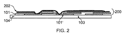
The
図2に、基板104の面103を保護する多層コーティングバリア200の実施例を模式的に例示する。多層コーティングバリア200は、第1の材料からなる二次元小板101’の第1の層101、および第2の層202を含む。第2の層は、コーティング層、例えば、原子層堆積法(ALD)により第1の層の平坦化面の最上部上に成長させた薄膜のコンフォーマルなコーティング層である。ある実施例では、第2の層は、酸化アルミニウムまたはアルミナ等のアルミニウムを用いたALDコーティングを含む。コンフォーマルなコーティングである第2の層は、その他の金属化合物(例えば金属の、酸化物、窒化物、およびスルフィド)を含む可能性があり、これらの金属化合物をALDにより成長させることができることが理解される。
FIG. 2 schematically illustrates an example of a
ALDコーティング、またはその他のコンフォーマルなコーティング層により、浸透性の極めて低い水/酸素バリアを提供することができる。しかしながら典型的には、特にポリマー基板については、基板中の面欠陥が、高品質でピンホールのないコンフォーマルなALDコーティング(またはその他のコンフォーマルなコーティング層)の成長を阻害する。第1の材料からなる二次元小板の初期層を設けると、平坦化面が生成され、これにより有利なことには、後続の層の優先成長が可能になる。例えば、高品質でピンホールがない、コンフォーマルとなるコーティング/ALDコーティングを、小板材料からなる第1の層の平坦化面上に成長させることができる。 An ALD coating, or other conformal coating layer, can provide a water / oxygen barrier with very low permeability. Typically, however, particularly for polymer substrates, surface defects in the substrate inhibit the growth of high quality, pinhole free conformal ALD coatings (or other conformal coating layers). Providing an initial layer of a two-dimensional platelet of the first material creates a planarized surface, which advantageously allows subsequent growth of subsequent layers. For example, a high quality, pinhole free, conformal coating / ALD coating can be grown on the planarized surface of the first layer of platelet material.
ALDコーティング/膜の層は、二次元小板が基板に結合するのを助けることができ、これによりハイブリッド多層コーティングの一体性を向上させる。 The layer of ALD coating / film can help the two-dimensional platelets bond to the substrate, thereby improving the integrity of the hybrid multilayer coating.
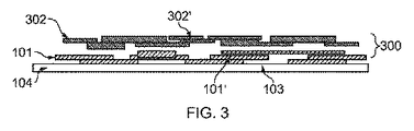
図3に、基板104の面103を保護する多層コーティングバリア300の実施例を模式的に例示する。多層コーティングバリア300は、第1の材料からなる複数の二次元小板101’を含む第1の層101、および第2の材料からなる複数の二次元小板302’を含む第2の層302を含み、第2の材料は第1の材料とは異なっており、これによりハイブリッド多層コーティングが提供される。第2の材料は、例えば、酸化グラフェン、窒化ホウ素、グラフェン、官能化グラフェン、フルオログラフェン、二硫化モリブデン、または小板の形態をとる無機材料、の1つを含むことができる。
FIG. 3 schematically illustrates an example of a
親水性小板、例えば酸化グラフェン(GO)の薄片を用いて超透水性の層/膜を提供するように、第1のおよび第2の材料のうちの一方を選択することができる。超透水性ではあるがその他のいかなる分子にも不透過性である層/膜を形成するために、GO溶液を、スプレー塗布、スピン塗布、スロットダイ塗布、ブレードまたはロッド塗布、エアナイフ塗布、ドロップキャスト、または印刷技術により塗布することができる。 One of the first and second materials can be selected to provide a superpermeable layer / membrane using a hydrophilic platelet, eg, a graphene oxide (GO) flake. To form a layer / film that is superpermeable but impermeable to any other molecule, the GO solution is spray coated, spin coated, slot die coated, blade or rod coated, air knife coated, drop cast Or by printing techniques.
第1のおよび第2の材料のうちもう一方を選択して、疎水性小板、例えば窒化ホウ素(BN)、グラフェン、またはフルオログラフェンの薄片を用いて、不透水性の層/膜が提供されるようにすることができる。そうした材料の溶液を、スロットダイ塗布、エアナイフ塗布、ロッド塗布、スプレー塗布、スピン塗布、ドロップキャスト、または印刷技術により塗布して、不透水性ではあるが有機分子には透過性である層/膜を形成することができる。 The other of the first and second materials is selected to provide a water impermeable layer / film using hydrophobic platelets, eg, boron nitride (BN), graphene, or fluorographene flakes You can make it. Layers / films that are impermeable but permeable to organic molecules by applying solutions of such materials by slot die coating, air knife coating, rod coating, spray coating, spin coating, drop casting, or printing techniques Can be formed.
2つのタイプの層/膜を組み合わせて多層構造にすることができ、この場合には疎水性の層/膜が水をはじき、親水性の層/膜が油および有機溶媒をはじく。 The two types of layers / membranes can be combined into a multilayer structure, where the hydrophobic layer / membrane repels water and the hydrophilic layer / membrane repels oil and organic solvents.
層の導電性は、グラフェン溶液を用いて提供される可能性があり、この溶液によって不透水性の膜が提供され得る。 The conductivity of the layer can be provided using a graphene solution, which can provide an impermeable membrane.
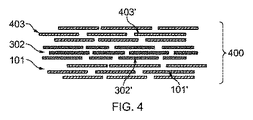
図4に、多層コーティングバリア400の実施例を例示するが、この多層コーティングバリアでは、以降の印刷または塗布技術によって、異なる層/膜101、102、403を、互いの最上部に積層することができる。多層コーティングバリア400は、
第1の材料からなる二次元小板101’の第1の層101、
前記第1の層を覆う、第2の材料からなる二次元小板302’の第2の層302、および
前記第2の層を覆う、第3の材料からなる二次元小板403’の第3の層403を含む。
FIG. 4 illustrates an example of a
A
A
さらなる層(図示せす)、例えば、ALD、またはその他の真空成長法、例えば、スパッタリング、蒸着、プラズマ成長、化学気相成長(CVD)、により成長させたコンフォーマルなコーティングを提供することができる。 Conformal coatings grown by additional layers (not shown), such as ALD, or other vacuum growth methods such as sputtering, evaporation, plasma growth, chemical vapor deposition (CVD) can be provided. .
第1の材料は、第2の材料とは異なることができ、そして第2の材料は、第3の材料とは異異なることができる。 The first material can be different from the second material, and the second material can be different from the third material.
第1の、第2の、そして第3の材料の1つ以上を選択することによって、不透水性/疎水性の層を提供することができ、第1の、第2の、そして第3の材料からなる別の1つ以上を選択することによって、透水性/親水性の層を提供することができる。図4の実施例においては、GO小板302’の透水性の層302は、BN小板403’および101’の不透水性の二層403および101の間に挟まれている。BN上層403は湿気に対して疎水性バリアとして働く一方、この層をかろうじて透過するいかなる水も、BN下層101によってGO中間層302に封じ込められる。
By selecting one or more of the first, second and third materials, an impermeable / hydrophobic layer can be provided, the first, second and third By selecting another one or more of materials, a water permeable / hydrophilic layer can be provided. In the embodiment of FIG. 4, the water
この装置のある実施例においては、これらの層の1つの層を、汚染要因物(例えば水分子、ガス粒子、あるいは有機分子)を取り去る、または汚染要因物を層の1つの領域から層の別の領域へ取り込むように、構成/構造化することができる。 In some embodiments of the apparatus, one of these layers may be removed from contaminants (eg, water molecules, gas particles, or organic molecules), or the contaminants may be separated from one region of the layer. Can be configured / structured to be captured in a region.
そうした層が、親水性材料、例えばGOの薄片から形成されている場合には、その層/膜は、水をコーティングから抽出する毛管媒質として作用する。親水性の層/膜は、水分子の流れを、層の周辺または装置の外部に向けて導く(そして層の中心領域または装置の内部へ向かう水分子の流れを阻害する)目的で、構造化することができる。このように、保護バリア層は、微量の水を除去する固有能力を提供することができる。 If such a layer is formed from a hydrophilic material, such as a slice of GO, the layer / membrane acts as a capillary medium for extracting water from the coating. A hydrophilic layer / membrane is structured for the purpose of directing the flow of water molecules towards the periphery of the layer or outside of the device (and hindering the flow of water molecules towards the central region of the layer or the inside of the device) can do. Thus, the protective barrier layer can provide the inherent ability to remove trace amounts of water.
親水性GO層は、水分子に対して超透過性であり、水分子を層の縁部へ拡散させることのできる低耐浸透性経路/高浸透性経路を生成することによって水を層の縁部へ誘導する/取り出すように、構成/構造化することができる。 The hydrophilic GO layer is super permeable to water molecules and allows water to flow through the edges of the layer by creating a low permeation / high permeability path that allows water molecules to diffuse to the edge of the layer. It can be configured / structured to be guided / removed to the part.
一実施例では、ある層を、親水性材料の通路/チャネルを画定する疎水性部分を含むように構成して、これにより親水性材料が、毛管媒質として働くようにすることができる。例えば、GO薄片の親水性層が、還元された酸化グラフェン(rGO)の領域を備えることができ、これは疎水性である。rGOは、GO層中で、GO層の一部の局所還元により得てもよい。GO層には、直接レーザー描画またはフラッシュ光照射によりパターン形成して光還元現象を利用するようにすることができ、これによりGOが照射時に還元してrGOに転化する。そのようなパターン形成を、単一の連続したGO層に適用して、疎水性で還元されたGOの部分/界面の間に画定される親水性のGOマイクロチャネル/毛管を生成するようにすることができる。チャネル/毛管を画定するためのrGOおよびGO上のパターン形成の幾何学形状は、層の外縁部に向かう水の流れにとって有利となる好適な幾何学形状であることができる。例えば、フラクタルな幾何学形状を設けてもよく、これは、層の中心/中間の領域から、その層の1つ以上の周辺領域または縁部へ向け分岐が増加している形状である。 In one example, a layer can be configured to include a hydrophobic portion that defines a passage / channel for the hydrophilic material, thereby allowing the hydrophilic material to act as a capillary medium. For example, the hydrophilic layer of a GO flake can comprise a region of reduced graphene oxide (rGO), which is hydrophobic. rGO may be obtained by local reduction of a part of the GO layer in the GO layer. The GO layer can be patterned directly by laser drawing or flash light irradiation to utilize the photoreduction phenomenon, whereby GO is reduced during irradiation and converted to rGO. Such patterning can be applied to a single continuous GO layer to produce hydrophilic GO microchannels / capillaries defined between hydrophobic and reduced GO portions / interfaces. be able to. The patterning geometry on the rGO and GO to define the channels / capillaries can be any suitable geometry that favors the flow of water towards the outer edge of the layer. For example, a fractal geometry may be provided, which is a shape with increasing branches from the center / intermediate region of the layer toward one or more peripheral regions or edges of the layer.
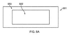
別の実施例では、層内の小板間の分離距離が選択的に変化するように、層を構成/構造化することができる。層内の小板間の鉛直分離距離は、特定分子に対する浸透性に影響を及ぼすことがある。したがって、鉛直分離距離を選択的に制御/調整して、特定分子に対する浸透性を制御することができる。例えば、図5Aおよび5Bに示すとおり、層の中心領域502に位置する隣接小板間の平均の鉛直分離距離を、層の周辺領域503における隣接小板間の平均の鉛直分離距離とは異なるように構成することができる。
In another embodiment, the layers can be configured / structured such that the separation distance between the platelets in the layer is selectively varied. The vertical separation distance between platelets in the layer can affect the permeability to specific molecules. Therefore, the permeability to a specific molecule can be controlled by selectively controlling / adjusting the vertical separation distance. For example, as shown in FIGS. 5A and 5B, the average vertical separation distance between adjacent platelets located in the
GO層等の層内での小板の分離を、面の官能化により選択/調整して、毛管経路のサイズがGO層の中心から側部に向け縮小するようにすることができる。 Separation of platelets within a layer such as a GO layer can be selected / adjusted by surface functionalization so that the size of the capillary pathway decreases from the center of the GO layer toward the sides.
小板の積層の分離は、小板に付着している官能基の使用により制御することができ、この官能基は細密充填を防止するものである。官能基の鎖の長さを選択/調整して小板の分離を制御することができ、長鎖の官能基ほど間隔が広くなる結果となる。このように、小板間の毛管チャネルを制御した小板構造を生成して、例えば、層の中心ではより大きな小板分離を有し、層の縁部へ湿気を誘導するために縁部に向かっては徐々に分離が小さくなっていくハイブリッド構造を生成するようにできる(ここで湿気はその後、例えば、ゲッター粒子による吸収または吸着によって処理/排出される)。 Separation of the stack of platelets can be controlled by the use of functional groups attached to the platelets, which functional groups prevent fine packing. The separation of the platelets can be controlled by selecting / adjusting the chain length of the functional group, with the result that the longer the functional group, the wider the spacing. In this way, a platelet structure with controlled capillary channels between the platelets is created, for example, having a larger platelet separation at the center of the layer and at the edge to induce moisture to the edge of the layer. A hybrid structure with progressively smaller separation can be produced (where the moisture is then treated / exhausted, for example, by absorption or adsorption by getter particles).
図5Aおよび図5Bに、本発明の多層バリア・コーティングにおいて使用される二次元小板の層501の平面図および側面図をそれぞれ模式的に例示する。2つの官能化GO領域が印刷されており、層の中心領域502は、未処理のGOを含んでもよく、その一方で外部/周辺領域503は、部分還元されたGOを含むことができ、部分還元されたGOは、より小さな小板間距離を示すことが知られている。そうした構造は、光還元によって得てもよく、例えば、GOを全領域に印刷し、中心領域502をマスキングし、そして、例えばレーザー、フラッシュ光を周辺領域503に照射することによって、周辺領域におけるGOを少なくとも部分還元して、部分還元されたGOとすることができる。この層501では、小板の分離は、層502の中心で大きいことと比較して、層503の縁部に向かって減少する。
5A and 5B schematically illustrate a top view and a side view, respectively, of a
部分還元されたGOは、還元工程(主に酸素含有官能基の除去からなるもの)が部分的にしか実行されなかった(すなわち一部の酸素含有官能基が依然として存在するが、その程度は未処理のGOと比較すると少ない)材料である。部分還元されたGOの特性、例えば親水性は、官能基により直接影響を受け、したがって、改質された、したがって例えば部分還元されたGOは、未処理のGOよりも親水性が低いが、還元されたGOよりは高いであろう。 Partially reduced GOs were only partially subjected to the reduction process (consisting primarily of removal of oxygen-containing functional groups) (ie, some oxygen-containing functional groups still exist, but to a lesser extent). (Compared to processing GO). Properties of partially reduced GO, such as hydrophilicity, are directly affected by functional groups, and thus modified, eg, partially reduced GO, is less hydrophilic than untreated GO, but reduced Will be higher than the published GO.
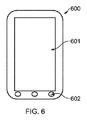
図6に、ディスプレイ601を備えた電子デバイス600を模式的に例示する。上記のような二次元小板の層を含む多層バリア・コーティングを、ディスプレイ601に適用して、力学的に可撓性で折り畳み可能なディスプレイデバイスを作り出せるようにすることができる。
FIG. 6 schematically illustrates an
本開示のある実施例は、1×10⁻⁶g/m2/日より多い水蒸気の侵入からOLEDを保護することができる、力学的に可撓性のあるバリア・コーティングを提供しようとするものである。そのような耐湿性は、充分な可撓性があり、フルカラーで、ビデオレートで動作可能な、力学的な撓みに耐久性を示すディスプレイの作製には大いに望ましいものである。 Certain embodiments of the present disclosure seek to provide a mechanically flexible barrier coating that can protect OLEDs from ingress of water vapor of greater than 1 × 10 −6 g / m 2 / day. It is. Such moisture resistance is highly desirable for making displays that are sufficiently flexible, full color, capable of operating at video rates and that are resistant to mechanical deflection.
デバイス600は、ユーザー入力部602も備えており、ユーザーは、この入力部を介してデバイスと対話しこれを制御することができる。ユーザー入力部602は、ここではボタンとして示されているが、ユーザー入力用のあらゆる手段、例えばタッチ感応画面、または音声入力を使用することができることが理解される。
The
電子デバイス600は、携帯式電子デバイスであってもよく、それらには、とりわけ、携帯電話、ワイヤレス通信デバイス、カメラ、携帯情報端末(PDA)、およびタブレットPCを挙げてもよい。携帯式電子デバイスは、オーディオ/テキスト/ビデオ通信の機能(例えば遠距離通信、ビデオ通信、および/またはテキスト伝送、ショートメッセージサービス(SMS)/マルチメディアメッセージサービス(MMS)/電子メールの機能、対話型/非対話型の鑑賞機能(例えばウェブ閲覧、ナビゲーション、TV/プログラム鑑賞の機能)、音楽の録音/再生の機能(例えばMP3またはその他の形式、および/または(FM/AM)ラジオ放送の録音/再生)、データのダウンロード/送信の機能、画像取り込み機能(例えばデジタルカメラ(内蔵等のもの)の使用によるもの)、並びにゲーム機能、の1つ以上を提供することができる。
The
ある特別な実施例では、二次元小板層は、伝導性材料、例えばグラフェン薄片からなるものであることができる。あるいは、この層の材料にドープして、伝導性が向上するようにすることができ、これは例えば、伝導性グラフェン原料をこの層に導入することにより行う。 In one particular embodiment, the two-dimensional platelet layer can be made of a conductive material, such as graphene flakes. Alternatively, the material of this layer can be doped to improve conductivity, for example by introducing a conductive graphene raw material into this layer.
バリア・コーティングは、機能的OLEDデバイスの電極としてさらに使用することによって、多機能性をもつように構成される可能性があり、例えばバリア・コーティングの導電層は、OLEDデバイスのアノードとして使用される可能性がある。有利なことには、バリア層は、保護バリアを提供するだけでなく、ディスプレイデバイス構造において必要な層の数を減少させるが、その理由は、独立したアノードが必要ないからである。さらに、グラフェン薄片を使用する場合、得られる電荷注入が向上することがあり、これにより、OLEDディスプレイデバイスの輝度/光出力、および効率が増大する。 The barrier coating may be configured to be multifunctional by further use as an electrode of a functional OLED device, for example, the conductive layer of the barrier coating is used as the anode of the OLED device there is a possibility. Advantageously, the barrier layer not only provides a protective barrier, but also reduces the number of layers required in the display device structure because a separate anode is not required. Furthermore, when graphene flakes are used, the resulting charge injection may be improved, which increases the brightness / light output and efficiency of the OLED display device.
本願のバリア・コーティングを、とりわけ例えば、保護バリア・コーティングを設けるために、可撓性基板105の面104、例えばOLEDディスプレイパネルに塗布することができる。可撓性基板105は、ポリマー基板、例えば、ポリ(エチレンテレフタレート)(PET)、またはポリエチレン2,6−ナフタレート(PEN)、ポリイミド(Polyilmide)(PI)、ポリアラミド(PA)、ポリエーテルエーテルケトン(PEEK)であることができる。
The barrier coating of the present application can be applied to the
実施例は、そうした品目に対するバリア・コーティングを設けることに関して議論したが、本願バリア・コーティングは、そのような用途には制限されないこと、そして、不動態化およびバリア保護を向上させるために、任意の表面、電子部品、または、環境や湿気に敏感な物体に塗布できることが理解される。例えばバリア・コーティングは、傷みやすい商品、太陽電池(PV)、および光学太陽(Optical Photo Voltaic)(OPV)電池用のパッケージに適用できる可能性がある。 While the examples discussed with respect to providing a barrier coating for such items, the present barrier coating is not limited to such applications, and any improvement may be made to improve passivation and barrier protection. It is understood that it can be applied to surfaces, electronic components, or objects sensitive to the environment and moisture. For example, barrier coatings may be applicable to packages for perishable products, solar cells (PV), and optical photovoltaic (OPV) cells.
図7に、本開示に係る方法700の実施例のフローチャートを模式的に例示する。ブロック701では、第1の材料からなる複数の二次元小板を含む第1の層が、面に設けられている。二次元小板は、スロットダイ塗布、エアナイフ塗布、ロッド塗布、スプレー塗布、スピンコート法、ドロップキャスト、または印刷技術により塗布することができる。
FIG. 7 schematically illustrates a flowchart of an embodiment of a
任意選択的に、ブロック702では、例えば、この層が、汚染要因物を層の1つの領域から層の別の領域へ誘導できるように、層を修正することができる。ブロック702Aでは、層内の小板の分離距離を選択的に調整することにより層を改質して、例えば、鉛直分離距離が、層の中心領域では層の周辺領域よりも大きくなるようにすることができる。小板の分離距離の制御は、第1の材料からなる層に官能基を導入する面の官能化により達成することができる。官能基の鎖の長さを選択して、小板の分離を制御することができ、これにより長鎖の基ほど長い小板分離距離が生じる。ブロック702Bでは、層を選択的に放射線照射して、例えば配列したチャネル/通路/毛管を有する層をパターン形成し、汚染要因物(例えば水分子または有機分子)を層の中心領域から周辺領域に誘導するように、層を改質することができる。
Optionally, at
ブロック703では、第2の層が第1の層の最上部に設けられる。第2の層は、二次元小板の別の層であって第1の材料とは異なる第2の材料からなる層であることができる(例えば一方の材料が親水性であってもう一方が疎水性となるようにすることができる)。第2の層は、代わりにコンフォーマルなコーティング、例えばALDコーティング層であることができる。 In block 703, a second layer is provided on top of the first layer. The second layer may be another layer of the two-dimensional platelet and may be a layer made of a second material different from the first material (for example, one material may be hydrophilic) Can be made hydrophobic). The second layer can alternatively be a conformal coating, such as an ALD coating layer.
さらなる1つの層以上の層、例えばさらなる二次元小板層、またはコンフォーマルなコーティング層を、さらに設けることができる。 Further one or more layers, for example a further two-dimensional platelet layer, or a conformal coating layer can further be provided.
図7の流れ図に、数あるうち考えうる1つのシナリオを表す。示されたブロックの順番は、絶対にそうであらねばならないというわけではなく、1つ以上のブロックを、異なった順番でまたは時間的に重ねて、連続的にまたは平行して実行することができる。1つ以上のブロックを省略(例えばブロック702、702A、および702B)、または追加、または幾通りかの組み合わせ方で変更することができる。 The flowchart of FIG. 7 shows one possible scenario. The order of the blocks shown does not have to be the case, and one or more blocks can be executed sequentially or in parallel, in different orders or in time. . One or more blocks may be omitted (eg, blocks 702, 702A, and 702B) or added or modified in some combination.
例えば、別のシナリオでは、成膜に先立って、異なる官能基を溶液中に既に提供してあってもよい。異なるように官能化された二次元小板を、異なった領域に印刷して、疎水性/親水性のパターンを設けるようにすることができる。このシナリオでは、改質ブロック702は、層成長ブロック701の前に現れる可能性がある、すなわち、或る層のための二次元小板材料を、層として成長させるのに先立って改質する。
For example, in another scenario, different functional groups may already be provided in the solution prior to film formation. Differently functionalized two-dimensional platelets can be printed in different areas to provide a hydrophobic / hydrophilic pattern. In this scenario, the
各ブロック、およびブロック同士の組み合わせは、特定の機能または工程を実行する特定用途向けのハードウェアベースのシステムを用いて実現することができることもまた理解される。したがって、これらのブロックは、指定された機能を実行する手段の組み合わせ、指定された機能を実行する工程の組み合わせ、および指定された機能を実行するコンピュータープログラム命令/アルゴリズムを支援する。 It is also understood that each block, and combinations of blocks, can be implemented using an application specific hardware based system that performs a specific function or process. Thus, these blocks support a combination of means for performing the specified function, a combination of steps for performing the specified function, and computer program instructions / algorithms for performing the specified function.
上記では、種々の積層を記載した。いかなる数の中間層も(中間層がないことも含めて)存在し得ることが理解されるべきである。 Above, various stacks have been described. It should be understood that any number of intermediate layers may be present (including no intermediate layers).
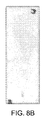
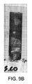
図8Aおよび8Bに、従来のバリア・コーティングについて実行された「カルシウムミラー」試験を例示する。一方、図9A〜9Bには、本開示に係る装置の実施例に準拠したバリア・コーティングについて実施した「カルシウムミラー」試験を例示する。 8A and 8B illustrate a “calcium mirror” test performed on a conventional barrier coating. On the other hand, FIGS. 9A-9B illustrate a “calcium mirror” test performed on a barrier coating in accordance with an embodiment of the apparatus according to the present disclosure.
カルシウムミラー試験では、ポリマー基板上、この場合ではポリエチレン2,6−ナフタレート(PEN)基板上での様々な材料のバリア特性を定量化する。 The calcium mirror test quantifies the barrier properties of various materials on a polymer substrate, in this case a polyethylene 2,6-naphthalate (PEN) substrate.
試験することになるバリア・コーティングは、PEN基板上に成長させる。次に、金属カルシウムの薄層をバリア・コーティングの最上部上に蒸着させ、この基板をその後、不透過ガラス基板に接着/積層して、水および酸素の侵入点がPEN+バリアを通してのみとなるようにする。この工程は、不活性雰囲気のグローブボックス中で行う。続いて、この試料を周囲条件中に持ち出し、カルシウムミラーの透明度を追跡することによりバリア特性を評価する。 The barrier coating to be tested is grown on the PEN substrate. Next, a thin layer of metallic calcium is deposited on top of the barrier coating and this substrate is then bonded / laminated to an impervious glass substrate so that water and oxygen entry points are only through the PEN + barrier. To. This step is performed in a glove box with an inert atmosphere. Subsequently, the sample is taken out into ambient conditions and the barrier properties are evaluated by following the transparency of the calcium mirror.
成長の直後では、カルシウムは、高反射率の銀ミラーを形成する。わずかな量の湿気または酸素があっても、金属カルシウムから透明な水酸化カルシウムへの転換が生じ、これにより透明なスポットが、湿気または酸素がバリアを透過した場所に出現する。 Immediately after growth, calcium forms a highly reflective silver mirror. Even in the presence of a small amount of moisture or oxygen, a conversion from metallic calcium to clear calcium hydroxide occurs, whereby a clear spot appears where moisture or oxygen has penetrated the barrier.
図8Aに、PEN基板の試料を示すが、これは、5nmのALDアルミナ層バリアの標準コーティングを有し、作製のすぐ後、試験開始時のものである。カルシウムの中心区域が、明瞭に視認できる。図8Bに、図8Aの5nmのALD試験試料を有するPENを示すが、これは、周囲条件中で24時間後のものである。アルミナバリアしか伴わないこの試料は、24時間後には完全に透明であり、これは、すべての金属カルシウムが酸素または湿気の侵入により消費されたことを示している。 FIG. 8A shows a sample of a PEN substrate that has a standard coating of 5 nm ALD alumina layer barrier, immediately after fabrication, at the start of the test. The central area of calcium is clearly visible. FIG. 8B shows the PEN with the 5 nm ALD test sample of FIG. 8A, after 24 hours in ambient conditions. This sample with only an alumina barrier is completely transparent after 24 hours, indicating that all metallic calcium has been consumed by oxygen or moisture ingress.
図9Aに、試験開始時の別の試料を示す。この試料は、GO小板の層をさらに含んでおり、すなわちPEN基板はGO小板に覆われており、その上に5nmのALDアルミナ層バリアが設けられている。作製後の始めのうちは、カルシウムの中心区域が明瞭に視認できる。図9Bに、図9AのGO小板および5nmのALDアルミナ試験試料を有するPENを示すが、これは、周囲条件中で24時間後のものである。この試料は、アルミナ層の下にGO小板を有しており、劣化しているのは小領域でしかなく、金属カルシウムの大部分は未反応のままであり、湿気および酸素から保護されている。 FIG. 9A shows another sample at the start of the test. The sample further includes a layer of GO platelets, i.e., the PEN substrate is covered with GO platelets, on which a 5 nm ALD alumina layer barrier is provided. In the beginning after fabrication, the central area of calcium is clearly visible. FIG. 9B shows a PEN with the GO platelet of FIG. 9A and a 5 nm ALD alumina test sample, after 24 hours in ambient conditions. This sample has a GO platelet under the alumina layer, it is only a small area that is degraded, and most of the metallic calcium remains unreacted and protected from moisture and oxygen. Yes.
図10Aに、図9Aの、すなわち試験開始時の試験試料を200倍で撮影した透過型光学顕微鏡画像を示す。図10Bに、図9Bの、すなわち試験の24時間後での試験試料を200倍で撮影した透過型光学顕微鏡画像を示す。これらの光学顕微鏡写真画像は、向上したバリア特性がGO小板に局在していることを示しているが、それは、金属カルシウムが小板間の露出領域で反応して透明であるのが確認されるからである。 FIG. 10A shows a transmission optical microscope image of the test sample in FIG. FIG. 10B shows a transmission optical microscope image of the test sample of FIG. 9B taken at 200 ×, ie 24 hours after the test. These optical micrograph images show that the improved barrier properties are localized in the GO platelets, which confirms that the metallic calcium reacts in the exposed areas between the platelets and is transparent Because it is done.
前記の特性は、明示的に記載された組み合わせ以外の組み合わせで利用することができる。 The above characteristics can be used in combinations other than those explicitly described.
複数の特徴を、ある実施例を参照して記載してきたが、これらの特性は、その他の実施例においても、記載の有無にかかわらず存在することができる。所与の実施例を、特許請求された発明の範囲から逸脱することなく変更するのが可能であることは理解されるべきである。 Although multiple features have been described with reference to certain embodiments, these characteristics can exist in other embodiments with or without the description. It should be understood that changes may be made in the given embodiments without departing from the scope of the claimed invention.
用語「含む」は、本文献内では、排他的ではなく包含的な意味で使用する。すなわち、Yを含むXに言及するいかなるものでも、Xがただ1つのXを含むことができる、または1つより多いXを含むことができることを示す。 The term “comprising” is used in this document in an inclusive rather than exclusive sense. That is, anything that refers to X, including Y, indicates that X can include only one X, or can include more than one X.
この簡潔な記載において、種々の実施例に言及してきた。ある実施例に関連した特性または機能を記載するということは、これらの特性または機能がその実施例中に存在していることを意味している。本文中での用語「実施例」、または「例えば」、または「〜することができる」を使用するということは、明示的に宣言されているかどうかにかかわらず、そうした特性または機能が、少なくとも記載の実施例中には、実施例として記載されているかどうかにかかわらず存在すること、そしてそれらが、その他の実施例の一部またはすべてに存在し得るが必ずしも存在しているわけではないことを意味している。こうして、「実施例」、「例えば」、または「〜することができる」は、実施例の集合における具体的な実例に言及する。その実例の性質は、その実例のみの性質、またはその集合の性質、またはその集合における一部のしかしすべてではない実例を含む下位集合の性質であることができる。 In this brief description, reference has been made to various embodiments. To describe characteristics or functions associated with an embodiment means that these characteristics or functions are present in that embodiment. The use of the terms “examples” or “for example” or “can be” in the text, whether or not explicitly declared, at least describes such characteristics or functions. Are present in the examples, whether or not they are described as examples, and they may be present in some or all of the other examples, but not necessarily present. I mean. Thus, “Example”, “for example”, or “can be” refers to a specific example in the set of examples. The property of the instance can be the property of the instance only, or the property of the set, or the property of a subset that includes some but not all instances in the set.
前述の明細書中では、特に重要であると考えられる本発明のそれらの特性に関心が向けられるよう努めたが、その一方で、図面においてここまでに言及したおよび/または示した、特許性のあるあらゆる特性または特性の組み合わせに関して、それらに特に重点が置かれてきたか否かにかかわらず、本出願人が保護を主張することは理解されるべきである。 In the foregoing specification, efforts have been made to draw attention to those features of the invention believed to be particularly important, while the patentable features previously mentioned and / or shown in the drawings. It should be understood that for any particular property or combination of properties, Applicant claims protection regardless of whether or not particular emphasis has been placed on them.
Claims (27)
前記第1の層を被覆する別の少なくとも1つの層と、
を備える装置であって、
表面に対するバリア・コーティングを形成するように構成される装置。 A first layer comprising a plurality of two-dimensional platelets made of a first material;
At least one other layer covering the first layer;
A device comprising:
A device that is configured to form a barrier coating to a surface.
酸化グラフェン、窒化ホウ素、グラフェン、官能化グラフェン、フルオログラフェン、遷移金属ジカルコゲナイド、二硫化モリブデン、シリレン、マイカ、ベントナイトクレイ、または小板の形態をとる無機材料、
のうちの1つを含む、請求項1に記載の装置。 The first material is
Inorganic materials in the form of graphene oxide, boron nitride, graphene, functionalized graphene, fluorographene, transition metal dichalcogenide, molybdenum disulfide, silylene, mica, bentonite clay, or platelets,
The apparatus of claim 1, comprising one of:
酸化グラフェン、窒化ホウ素、グラフェン、官能化グラフェン、フルオログラフェン、遷移金属ジカルコゲナイド、二硫化モリブデン、シリレン、マイカ、ベントナイトクレイ、または小板の形態をとる無機材料、
のうちの1つを含む、請求項4に記載の装置。 The second material is
Inorganic materials in the form of graphene oxide, boron nitride, graphene, functionalized graphene, fluorographene, transition metal dichalcogenide, molybdenum disulfide, silylene, mica, bentonite clay, or platelets,
The apparatus of claim 4, comprising one of:
第1の材料からなる複数の二次元小板を含む第1の層を前記表面に設けること、および
別の少なくとも1つの層を用いて前記第1の層を被覆すること、が結果として得られる作用を、少なくともある程度まで生じさせることを含む方法。 A method of providing a barrier coating on the surface,
Providing the surface with a first layer comprising a plurality of two-dimensional platelets made of a first material and covering the first layer with another at least one layer results. Causing the effect to occur to at least some extent.
Applications Claiming Priority (3)
| Application Number | Priority Date | Filing Date | Title |
|---|---|---|---|
| GB1401506.9A GB2522626A (en) | 2014-01-29 | 2014-01-29 | Apparatus and method for providing barrier coating |
| GB1401506.9 | 2014-01-29 | ||
| PCT/FI2015/050032 WO2015114205A1 (en) | 2014-01-29 | 2015-01-21 | A barrier coating |
Publications (1)
| Publication Number | Publication Date |
|---|---|
| JP2017511955A true JP2017511955A (en) | 2017-04-27 |
Family
ID=50287743
Family Applications (1)
| Application Number | Title | Priority Date | Filing Date |
|---|---|---|---|
| JP2016549137A Pending JP2017511955A (en) | 2014-01-29 | 2015-01-21 | Barrier coating |
Country Status (5)
| Country | Link |
|---|---|
| EP (1) | EP3100314A4 (en) |
| JP (1) | JP2017511955A (en) |
| CN (1) | CN106062987A (en) |
| GB (1) | GB2522626A (en) |
| WO (1) | WO2015114205A1 (en) |
Cited By (1)
| Publication number | Priority date | Publication date | Assignee | Title |
|---|---|---|---|---|
| KR20190053313A (en) * | 2017-11-09 | 2019-05-20 | 삼성디스플레이 주식회사 | Display device and manufacturing method of the same |
Families Citing this family (5)
| Publication number | Priority date | Publication date | Assignee | Title |
|---|---|---|---|---|
| US10547032B2 (en) * | 2014-07-31 | 2020-01-28 | Lorea Institute Of Industrial Technology | Film comprising graphene oxide and clay, preparation method therefor, and use thereof as oxygen barrier film |
| EP3632676A1 (en) * | 2018-10-02 | 2020-04-08 | Ventus Engineering GmbH | Layered structure with multiple layers, use of and method therefore |
| WO2020070183A1 (en) * | 2018-10-02 | 2020-04-09 | Ventus Engineering GmbH | Layered structure with multiple layers, use of and method therefore |
| CN109755411A (en) * | 2019-01-14 | 2019-05-14 | 宁波石墨烯创新中心有限公司 | Packaging film and preparation method thereof, encapsulating structure and preparation method thereof |
| EP4073290A1 (en) * | 2019-12-09 | 2022-10-19 | Hewlett-Packard Development Company, L.P. | Coated metal alloy substrate and process for production thereof |
Citations (6)
| Publication number | Priority date | Publication date | Assignee | Title |
|---|---|---|---|---|
| JP2005216856A (en) * | 2004-02-02 | 2005-08-11 | Samsung Sdi Co Ltd | Organic el element |
| JP2007536169A (en) * | 2004-05-04 | 2007-12-13 | シグマ ラボラトリー オブ アリゾナ, インク. | Composite modular barrier structure and package |
| JP2010511267A (en) * | 2006-11-06 | 2010-04-08 | エージェンシー フォー サイエンス,テクノロジー アンド リサーチ | Nanoparticle-encapsulated barrier stack |
| WO2012002113A1 (en) * | 2010-06-29 | 2012-01-05 | コニカミノルタホールディングス株式会社 | Transparent conductor, organic el element, and organic photoelectric conversion element |
| JP2012504304A (en) * | 2008-09-30 | 2012-02-16 | コミサリア ア レネルジー アトミック エ オ ゼネルジー アルテルナティブ | Organic optoelectronic device and method for encapsulating said device |
| JP2013544012A (en) * | 2010-10-25 | 2013-12-09 | ネダーランゼ・オルガニサティ・フォーア・トゥーゲパスト−ナトゥールヴェテンシャッペリーク・オンデルゾエク・ティーエヌオー | Optoelectronic device and method of manufacturing optoelectronic device |
Family Cites Families (8)
| Publication number | Priority date | Publication date | Assignee | Title |
|---|---|---|---|---|
| US4818782A (en) * | 1987-07-30 | 1989-04-04 | E. I. Du Pont De Nemours And Company | Ethylene vinyl alcohol copolymers containing platelet-type mica fillers, processes for preparing same and multi-layer containers with layers thereof |
| AU2002367628A1 (en) * | 2001-01-29 | 2003-10-08 | The Board Of Regents For Oklahoma State University | Organic/inorganic multilayer coating system |
| US7449133B2 (en) * | 2006-06-13 | 2008-11-11 | Unidym, Inc. | Graphene film as transparent and electrically conducting material |
| FR2926302B1 (en) * | 2008-01-14 | 2014-03-07 | Eads Europ Aeronautic Defence | NANOSTRUCTURE ANTI-CORROSION COATING, STRUCTURE COMPRISING SAME, METHOD FOR ANTI-CORROSION PROTECTION OF A SUBSTRATE. |
| KR20110019636A (en) * | 2009-08-20 | 2011-02-28 | 삼성모바일디스플레이주식회사 | Substrate for flexible display, method of manufacturing the same and organic light emitting diode display including the substrate |
| KR100985782B1 (en) * | 2009-12-28 | 2010-10-06 | 한국과학기술원 | Method for manufacturing flexible substrates and food packaging film having water vapor and oxygen barrier properties |
| US9272497B2 (en) * | 2010-07-22 | 2016-03-01 | Ferro Corporation | Hermetically sealed electronic device using coated glass flakes |
| US8999497B2 (en) * | 2011-12-13 | 2015-04-07 | Samsung Electronics Co., Ltd. | Barrier film for electronic device and method of manufacturing the same |
-
2014
- 2014-01-29 GB GB1401506.9A patent/GB2522626A/en not_active Withdrawn
-
2015
- 2015-01-21 WO PCT/FI2015/050032 patent/WO2015114205A1/en active Application Filing
- 2015-01-21 JP JP2016549137A patent/JP2017511955A/en active Pending
- 2015-01-21 CN CN201580006285.2A patent/CN106062987A/en active Pending
- 2015-01-21 EP EP15743892.0A patent/EP3100314A4/en not_active Withdrawn
Patent Citations (6)
| Publication number | Priority date | Publication date | Assignee | Title |
|---|---|---|---|---|
| JP2005216856A (en) * | 2004-02-02 | 2005-08-11 | Samsung Sdi Co Ltd | Organic el element |
| JP2007536169A (en) * | 2004-05-04 | 2007-12-13 | シグマ ラボラトリー オブ アリゾナ, インク. | Composite modular barrier structure and package |
| JP2010511267A (en) * | 2006-11-06 | 2010-04-08 | エージェンシー フォー サイエンス,テクノロジー アンド リサーチ | Nanoparticle-encapsulated barrier stack |
| JP2012504304A (en) * | 2008-09-30 | 2012-02-16 | コミサリア ア レネルジー アトミック エ オ ゼネルジー アルテルナティブ | Organic optoelectronic device and method for encapsulating said device |
| WO2012002113A1 (en) * | 2010-06-29 | 2012-01-05 | コニカミノルタホールディングス株式会社 | Transparent conductor, organic el element, and organic photoelectric conversion element |
| JP2013544012A (en) * | 2010-10-25 | 2013-12-09 | ネダーランゼ・オルガニサティ・フォーア・トゥーゲパスト−ナトゥールヴェテンシャッペリーク・オンデルゾエク・ティーエヌオー | Optoelectronic device and method of manufacturing optoelectronic device |
Cited By (3)
| Publication number | Priority date | Publication date | Assignee | Title |
|---|---|---|---|---|
| KR20190053313A (en) * | 2017-11-09 | 2019-05-20 | 삼성디스플레이 주식회사 | Display device and manufacturing method of the same |
| KR102483236B1 (en) * | 2017-11-09 | 2022-12-30 | 삼성디스플레이 주식회사 | Display device and manufacturing method of the same |
| US11832503B2 (en) | 2017-11-09 | 2023-11-28 | Samsung Display Co. Ltd. | Display device and method for manufacturing the same |
Also Published As
| Publication number | Publication date |
|---|---|
| EP3100314A1 (en) | 2016-12-07 |
| CN106062987A (en) | 2016-10-26 |
| EP3100314A4 (en) | 2017-09-13 |
| GB2522626A (en) | 2015-08-05 |
| WO2015114205A1 (en) | 2015-08-06 |
| GB201401506D0 (en) | 2014-03-12 |
Similar Documents
| Publication | Publication Date | Title |
|---|---|---|
| JP2017511955A (en) | Barrier coating | |
| Carcia et al. | Permeation measurements and modeling of highly defective Al2O3 thin films grown by atomic layer deposition on polymers | |
| CN105734493B (en) | The forming method of metal oxide film and metal oxide film | |
| EP2238632A1 (en) | Device comprising an encapsulation unit | |
| US20150044442A1 (en) | Flexible substrate and method for preparing the same | |
| US20130045374A1 (en) | Nano-laminated film with transparent conductive property and water-vapor resistance function and method thereof | |
| JP2010511267A (en) | Nanoparticle-encapsulated barrier stack | |
| JP2020035749A (en) | Encapsulation of organic optoelectronic component | |
| US10644259B2 (en) | Package of electronic device and display panel | |
| KR20180134923A (en) | Separation method and manufacturing method of flexible device | |
| CN106887407A (en) | Flexible electronic device and its manufacture method | |
| Kidambi et al. | Multifunctional oxides for integrated manufacturing of efficient graphene electrodes for organic electronics | |
| Wang et al. | Flash-welded ultraflat silver nanowire network for flexible organic light-emitting diode and triboelectric tactile sensor | |
| TW201243969A (en) | Conductive film having oxide layer and method for manufacturing thereof | |
| Kim et al. | A compact polymer–inorganic hybrid gas barrier nanolayer for flexible organic light-emitting diode displays | |
| Wang et al. | Electrical bistability by self-assembled gold nanoparticles in organic diodes | |
| Coloma Ribera et al. | Determination of oxygen diffusion kinetics during thin film ruthenium oxidation | |
| Wegler et al. | Influence of PEDOT: PSS on the effectiveness of barrier layers prepared by atomic layer deposition in organic light emitting diodes | |
| JP2011207018A (en) | Gas barrier film and method for manufacturing the same | |
| Koike et al. | Multilayer transparent electrode consisting of silver alloy layer and metal oxide layers for organic luminescent electronic display device | |
| Kim et al. | Passivation effects on the stability of pentacene thin-film transistors with SnO2 prepared by ion-beam-assisted deposition | |
| KR101083551B1 (en) | Passivation thin film | |
| Ali et al. | Al2O3 coatings fabrication on silver nanowires through low temperature atomic layer deposition | |
| Lee et al. | Hygroscopic fluorine‐doped silicon oxide thin‐film‐based large‐area three‐layered moisture barrier using a roll‐to‐roll microwave plasma‐enhanced chemical vapor deposition system | |
| WO2021205410A1 (en) | Display panel having blind hole to accommodate signals exchanged with under-display component |
Legal Events
| Date | Code | Title | Description |
|---|---|---|---|
| A131 | Notification of reasons for refusal |
Free format text: JAPANESE INTERMEDIATE CODE: A131 Effective date: 20170801 |
|
| A977 | Report on retrieval |
Free format text: JAPANESE INTERMEDIATE CODE: A971007 Effective date: 20170731 |
|
| A521 | Request for written amendment filed |
Free format text: JAPANESE INTERMEDIATE CODE: A523 Effective date: 20171027 |
|
| A02 | Decision of refusal |
Free format text: JAPANESE INTERMEDIATE CODE: A02 Effective date: 20180227 |