JP2017509059A - Synchronize interrupt handling to reduce power consumption - Google Patents
Synchronize interrupt handling to reduce power consumption Download PDFInfo
- Publication number
- JP2017509059A JP2017509059A JP2016550205A JP2016550205A JP2017509059A JP 2017509059 A JP2017509059 A JP 2017509059A JP 2016550205 A JP2016550205 A JP 2016550205A JP 2016550205 A JP2016550205 A JP 2016550205A JP 2017509059 A JP2017509059 A JP 2017509059A
- Authority
- JP
- Japan
- Prior art keywords
- interrupt
- core
- delay
- pending
- processor
- Prior art date
- Legal status (The legal status is an assumption and is not a legal conclusion. Google has not performed a legal analysis and makes no representation as to the accuracy of the status listed.)
- Pending
Links
- 230000003111 delayed effect Effects 0.000 claims abstract description 33
- 238000000034 method Methods 0.000 claims description 46
- 230000002093 peripheral effect Effects 0.000 claims description 23
- 230000008569 process Effects 0.000 claims description 13
- 230000007704 transition Effects 0.000 claims description 13
- 238000001514 detection method Methods 0.000 claims description 8
- 230000004044 response Effects 0.000 claims description 5
- 238000010586 diagram Methods 0.000 description 15
- 230000000737 periodic effect Effects 0.000 description 8
- 238000004891 communication Methods 0.000 description 7
- 229910003460 diamond Inorganic materials 0.000 description 7
- 239000010432 diamond Substances 0.000 description 7
- 230000001934 delay Effects 0.000 description 5
- 230000001413 cellular effect Effects 0.000 description 3
- 230000001960 triggered effect Effects 0.000 description 3
- 230000005540 biological transmission Effects 0.000 description 2
- 239000000872 buffer Substances 0.000 description 2
- 238000013500 data storage Methods 0.000 description 2
- 230000000694 effects Effects 0.000 description 2
- 238000012986 modification Methods 0.000 description 2
- 230000004048 modification Effects 0.000 description 2
- 230000003287 optical effect Effects 0.000 description 2
- 230000001360 synchronised effect Effects 0.000 description 2
- 238000003491 array Methods 0.000 description 1
- 239000004744 fabric Substances 0.000 description 1
- 230000006870 function Effects 0.000 description 1
- 230000000977 initiatory effect Effects 0.000 description 1
- 230000009249 intrinsic sympathomimetic activity Effects 0.000 description 1
- 230000007774 longterm Effects 0.000 description 1
- 230000009467 reduction Effects 0.000 description 1
- 239000004065 semiconductor Substances 0.000 description 1
- 239000007787 solid Substances 0.000 description 1
- 230000003068 static effect Effects 0.000 description 1
Images


Classifications
-
- G—PHYSICS
- G06—COMPUTING; CALCULATING OR COUNTING
- G06F—ELECTRIC DIGITAL DATA PROCESSING
- G06F13/00—Interconnection of, or transfer of information or other signals between, memories, input/output devices or central processing units
- G06F13/14—Handling requests for interconnection or transfer
- G06F13/20—Handling requests for interconnection or transfer for access to input/output bus
- G06F13/24—Handling requests for interconnection or transfer for access to input/output bus using interrupt
-
- G—PHYSICS
- G06—COMPUTING; CALCULATING OR COUNTING
- G06F—ELECTRIC DIGITAL DATA PROCESSING
- G06F2213/00—Indexing scheme relating to interconnection of, or transfer of information or other signals between, memories, input/output devices or central processing units
- G06F2213/24—Interrupt
- G06F2213/2404—Generation of an interrupt or a group of interrupts after a predetermined number of interrupts
-
- G—PHYSICS
- G06—COMPUTING; CALCULATING OR COUNTING
- G06F—ELECTRIC DIGITAL DATA PROCESSING
- G06F2213/00—Indexing scheme relating to interconnection of, or transfer of information or other signals between, memories, input/output devices or central processing units
- G06F2213/24—Interrupt
- G06F2213/2406—Generation of an interrupt or a group of interrupts after a fixed or calculated time elapses
-
- Y—GENERAL TAGGING OF NEW TECHNOLOGICAL DEVELOPMENTS; GENERAL TAGGING OF CROSS-SECTIONAL TECHNOLOGIES SPANNING OVER SEVERAL SECTIONS OF THE IPC; TECHNICAL SUBJECTS COVERED BY FORMER USPC CROSS-REFERENCE ART COLLECTIONS [XRACs] AND DIGESTS
- Y02—TECHNOLOGIES OR APPLICATIONS FOR MITIGATION OR ADAPTATION AGAINST CLIMATE CHANGE
- Y02D—CLIMATE CHANGE MITIGATION TECHNOLOGIES IN INFORMATION AND COMMUNICATION TECHNOLOGIES [ICT], I.E. INFORMATION AND COMMUNICATION TECHNOLOGIES AIMING AT THE REDUCTION OF THEIR OWN ENERGY USE
- Y02D10/00—Energy efficient computing, e.g. low power processors, power management or thermal management
Landscapes
- Engineering & Computer Science (AREA)
- Theoretical Computer Science (AREA)
- Physics & Mathematics (AREA)
- General Engineering & Computer Science (AREA)
- General Physics & Mathematics (AREA)
- Power Sources (AREA)
- Bus Control (AREA)
- Software Systems (AREA)
- Debugging And Monitoring (AREA)
Abstract
プロセッサは、第1のコアを含む少なくとも1つのコア及び割込遅延論理を開示し、かつ、これらを含む。割込遅延論理は、第1の時点で第1の割り込みを受信し、第2の割り込みが第1のコアにより処理されるときに、第1の割り込みが第2の時点でペンディングされていない限り、第1の割り込みが処理されることを、第1の時点で開始する第1の時間遅延で遅延させる。第1の割り込みが第2の時点でペンディング中である場合、割込遅延論理は、第1の時間遅延の完了前に第1の割り込みの処理を開始することを第1のコアに指示する。他の実施形態が開示され、特許請求される。The processor discloses and includes at least one core including a first core and interrupt delay logic. The interrupt delay logic receives a first interrupt at a first time and, when the second interrupt is serviced by the first core, unless the first interrupt is pending at the second time The first interrupt is delayed by a first time delay starting at the first time point. If the first interrupt is pending at the second time point, the interrupt delay logic instructs the first core to begin processing the first interrupt prior to completion of the first time delay. Other embodiments are disclosed and claimed.
Description
実施形態は、割り込み処理に関連する。 Embodiments relate to interrupt handling.
例えば、スマートフォン、タブレット等の携帯デバイスのようなデバイスは、入力を提供し得る周辺デバイスの多様化の結果として生じる高レートの非同期イベントを有し得る。例えば、非同期イベントは、モーションセンサ、光センサ、タッチスクリーン等を含み得る。また、これらの携帯デバイスは、セルラーネットワークページング、周期的なタイマーイベント等に関連する周期的な割り込みのような同期イベントを受信し得る。 For example, devices such as mobile devices such as smartphones, tablets, etc. may have high rate asynchronous events that occur as a result of diversification of peripheral devices that may provide input. For example, asynchronous events can include motion sensors, light sensors, touch screens, and the like. These portable devices may also receive synchronization events such as periodic interrupts associated with cellular network paging, periodic timer events, and the like.
プロセッサに入力される割り込みメッセージ(「割り込み」)は、同期イベント及び非同期イベントに関連し、プロセッサに、スラッシングさせ、例えば、アクティブ状態とインアクティブ状態との間を過度に変動させる恐れがあり、次に、インアクティブからアクティブ状態への遷移の結果としての「ウェイクアップ」電力コストに起因する高い電力消費を引き起こす恐れがあり、その結果、例えば、バッテリ等の電源の再充電間の期間が短縮される可能性がある。 Interrupt messages ("interrupts") that are input to the processor are related to synchronous and asynchronous events and can cause the processor to thrash, for example, excessively fluctuate between active and inactive states, Can result in high power consumption due to the “wake-up” power cost as a result of the transition from inactive to active state, resulting in a reduced period between recharging of power sources such as batteries, for example. There is a possibility.
複数の割り込みソースは、ソースの特性及びソースから受信した複数の割り込みを処理するための要求に従って分類されることができる。例えば、いくつかの割り込み(本明細書における「ハード割り込み」又は「クリティカルな割り込み」、例えば、セルラー伝送規格に関連する、例えば、周期的な割り込み)は、処理する前に、意図的に遅延させられることなくサービス提供される。他の割り込み(本明細書における「ソフト割り込み」又は「非クリティカルな割り込み」)は、時間的制約が少なく、例えば、周辺デバイス/アプリケーション等の割り込みソースの性質に従って割り当てられる時間遅延で、意図的に遅延させることができる。 Multiple interrupt sources can be classified according to the characteristics of the source and the request to handle multiple interrupts received from the source. For example, some interrupts (“hard interrupts” or “critical interrupts” herein, eg, periodic interrupts related to cellular transmission standards, eg, periodic interrupts) are intentionally delayed before processing. Service is provided without being done. Other interrupts (“soft interrupts” or “non-critical interrupts” herein) are less time-constrained and are intentionally time delays assigned according to the nature of the interrupt source, eg, peripheral device / application, etc. Can be delayed.
実施形態において、プログラム可能な遅延値をイベントごと又は複数のイベントのグループごとに確立することができる。複数の割り込みは、プロセッサがインアクティブ(「スリープ」)状態からアクティブ化(「アウェイク化」)されたときに、プロセッサが複数の割り込みを処理(例えば、「バッチ処理」)することができるように、グループ化されることができる。複数の割り込みのバッチ処理は、プロセッサが特定の時間フレームで経験するアクティブ/インアクティブサイクルの総数を低減でき、プロセッサの全体的な消費電力を低くできる。 In an embodiment, a programmable delay value may be established for each event or group of events. Multiple interrupts allow the processor to handle multiple interrupts (eg, “batch processing”) when the processor is activated (“wakened”) from an inactive (“sleep”) state Can be grouped. Batch processing of multiple interrupts can reduce the total number of active / inactive cycles that the processor experiences in a particular time frame and can reduce the overall power consumption of the processor.
複数の実施形態において、プログラムされた遅延タイマー値は、例えば、プロセッサ及び/又はシステムオンチップ(SoC)が節電(インアクティブ)状態にあるときに、例えば、アドバンスドコンピューティングアンドパワーインタフェース(ACPI)パワーダウン状態C1〜C6のうちの1つにあるときに、(例えば、割り込みに関連するハンドラの実行を利用した)割り込み処理を遅延させるべく、オペレーティングシステムで利用可能である。様々なタイプの割り込みに対する複数のプログラムされた遅延値は、プロセッサ又はSoCの各インアクティブからアクティブへの遷移に起因して大きな電力消費を引き起こす可能性がある、各割り込みの個別処理の代わりに割り込み処理のバッチ処理を可能とする。実施形態において、割り込み処理は、各割り込みに割り当てられる対応する遅延時間に動的に基づいて複数のイベントを自動的にグループ化する。 In embodiments, the programmed delay timer value may be, for example, advanced computing and power interface (ACPI) power when the processor and / or system on chip (SoC) is in an inactive state, for example. Available in the operating system to delay interrupt processing (eg, using execution of a handler associated with an interrupt) when in one of the down states C1-C6. Multiple programmed delay values for different types of interrupts can cause significant power consumption due to each inactive-to-active transition of the processor or SoC, instead of individual handling of each interrupt Allows batch processing. In an embodiment, interrupt processing automatically groups multiple events based dynamically on the corresponding delay time assigned to each interrupt.
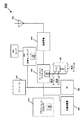
図1は、本発明の実施形態に係るシステム100のブロック図である。システム100は、1又は複数のコア1020−102N、割込コントローラ104及び割込遅延コントローラ106を含むプロセッサ110と、プロセッサ110に連結される複数の周辺デバイス1200−120Mと、プロセッサ110に連結されるダイナミックランダムアクセスメモリ(DRAM)130とを含む。
FIG. 1 is a block diagram of a
動作中、プロセッサ110は、周辺デバイス1200−120Mのうちの1又は複数から、複数の割り込みメッセージ(また、本明細書において「複数の割り込み」)を受信してよい。複数の割り込み(「ハード割り込み」)の1又は複数は、割り込みが、例えば、意図的に遅延させられずに、受信したときに処理されるための対応するハードリアルタイム割り込みイベントに関連してよい。例えば、ハード割り込みは、セルラー規格に関連する周期的なイベントに関連してよく、ハード割り込みは、例えば、意図的に時間遅延させられることなく、受信されると、プロセッサ110により処理される。
During operation, the
他の割り込みは、周期的(例えば、同期)又は非周期的(例えば、非同期)であってよいが、複数のハードリアルタイム割り込みイベントに関連しておらず、従って、そのような複数の割り込み(「ソフト割り込み」)の処理は、遅延させられてよい、例えば、意図的に時間を遅延させられてよい。例えば、複数の非同期の割り込みは、センサ入力、タッチスクリーン、周期的に受信され得るデータ等のような複数の非同期イベントに関連してよい。 Other interrupts may be periodic (eg, synchronous) or aperiodic (eg, asynchronous), but are not associated with multiple hard real-time interrupt events, and therefore, such multiple interrupts (“ The processing of “soft interrupts”) may be delayed, eg intentionally delayed in time. For example, multiple asynchronous interrupts may be associated with multiple asynchronous events such as sensor inputs, touch screens, data that can be received periodically, and the like.
複数のソフトイベントを作成する(例えば、複数のソフト割り込みを生成する)周辺デバイス1200−120Mごとに、各ソフト割り込みを処理する対応する時間遅延が割り当てられてよい。発信元の周辺デバイスから受信された複数のソフト割り込みを処理する時間遅延は、発信元の周辺デバイスの特性に基づいて判断されてよく、システム100の使用の前に判断されてよい。例えば、複数のソフト割り込みに対する許容可能な時間遅延の判断において考慮されるべき1つの要因は、関連するイベント発生の最悪ケースの周期(worst case frequency)であってよい。例えば、最悪ケース推定において、イベントが100ミリ秒毎に発生する場合、関連する割り込みを処理する100μsの遅延は、性能に対する影響を無視できる。時間遅延は、プロセッサ110による1又は複数の割り込みの受信前に、提供されてよい(例えば、プロセッサ110内に格納されてよい)。
For each peripheral device 120 0 -120 M that creates multiple soft events (eg, generates multiple soft interrupts), a corresponding time delay for processing each soft interrupt may be assigned. The time delay for processing multiple soft interrupts received from the originating peripheral device may be determined based on the characteristics of the originating peripheral device and may be determined prior to use of the
周辺デバイス1200−120Mの1又は複数から割込遅延コントローラ106により受信された複数のハード割り込みは、意図的に時間遅延させられることなく処理されるべく、割込コントローラ104に渡されてよい。ソフト割り込みがプロセッサ110により受信されたときに、割込遅延コントローラ106は、ソフト割り込みを提供した周辺デバイス120に基づいて、対応する時間遅延(例えば、割込遅延コントローラ106内に格納されている)を選択してよい。受信したソフト割り込みごとに、割込遅延コントローラは、例えば、対応するタイマーを用いて、対応する時間遅延のカウントを開始してよく、対応するタイマーが時間遅延の終了に至ったときに、ソフト割り込みは、割込コントローラ104へとリリースされてよく、ソフト割り込みは、コア1020−102Nのうちの1つにより処理されるべく、割込コントローラ104により振り分けられてよい。
Multiple hard interrupts received by the
実施形態において、ハード割り込みが、即時処理のためにプロセッサ110により受信されたときに、割込遅延コントローラ106は、いずれのソフト割り込みがペンディング中であるか否かを判断してよく、例えば、関連するタイマーが、ソフト割り込みに対する時間遅延をカウントすることを開始しており、かつ、そのカウントを完了していないかを判断してよい。割込遅延コントローラ106は、コア1020−102Nのうちの1つによる処理のために、例えば、関連するタイマーのカウントを完了することなく、1又は複数のペンディング中のソフト割り込みを割込コントローラ104へとリリースしてよい。コアによる処理のためにリリースされる複数の割り込みは、コアがアクティブである間、例えば、コアが、リリースされた全てのソフト割り込みの処理が完了するまでに、ハード割り込みが受信された時点からアクティブを維持している間、に処理される。
In embodiments, when a hard interrupt is received by the
別の実施形態において、第1のソフト割り込みは、タイマーの満了に起因して、例えば、関連するタイマーが各時間遅延のそのカウントを完了したことに起因して、コア1020−102Nのうちの第1のコアにより処理される。割込遅延コントローラ106は、各時間遅延のそれぞれの完了前に第1のコアに処理させるために、他の1又は複数のペンディング中のソフト割り込みを割込コントローラ104へとリリースしてよい。第1のコアによる処理のためにリリースされる複数の割り込みは、バッチ処理され、例えば、第1のソフト割り込みの処理の結果として、第1のコアがアクティブである間に処理される。コアは、リリースされた複数の割り込みの処理が完了するまでアクティブを維持する。
In another embodiment, the first soft interrupt is due to the expiration of a timer, eg, due to the associated timer completing its count of each time delay, out of cores 102 0 -102 N Of the first core. The
上記で説明した複数の実施形態のそれぞれにおいて、特定の割り込みが、処理されるべく、割込コントローラに送信されるときに、割込遅延コントローラ106は、コアの単一アクティブ期間の間に処理されるべく、1又は複数のペンディング中の割り込みをリリースしてよい。従って、特定のコアは、処理される割り込みごとにインアクティブとアクティブ状態との間を変動しない。複数の割り込みのバッチ処理は、スラッシングを低減することができ、さもなければ「ウェイクアップ」電力コストに起因して費やされることになるプロセッサの消費電力を低減することができる。つまり、複数の割り込みをバッチ処理することにより、処理される複数の割り込みに対して、ウェイクアップの複数の過程から単一のウェイクアップ過程となって、コアを再アクティブ化するために費やされる電力は、低減され得る。
In each of the embodiments described above, the
図2は、本発明の複数の実施形態に係る割込遅延コントローラ200のブロック図である。割込遅延コントローラ200は、時間遅延カウンタ2101−210Lと、時間遅延レジスタ2201−220Lと、割込検出論理224、カウンタ割当論理226、及びペンディング割込リリース論理228を含む割込遅延論理222とを含む。割込検出論理224、カウンタ割当論理226、及びペンディング割込リリース論理228を含む割込遅延論理222は、ソフトウェア、ハードウェア、ファームウェア又はこれらの組み合わせに実装されてよい。
FIG. 2 is a block diagram of an
動作中、複数の周辺デバイスは、割り込み2021−202jを生成してよい。いくつかの周辺デバイスから受信された複数の割り込みのいくつかは、例えば、意図的に遅延させられることなく処理される複数のハード割り込みであってよい。他の割り込みは、複数のソフト割り込みであってよく、処理の前に遅延させられてよい。 In operation, multiple peripheral devices may generate interrupts 202 1 -202 j . Some of the plurality of interrupts received from several peripheral devices may be, for example, a plurality of hard interrupts that are processed without intentional delay. Other interrupts may be multiple soft interrupts and may be delayed before processing.
割込検出論理224は、受信される各ハード割り込みを検出してよく、処理のために特定のコアに出力されるべく、遅延させることなく割込コントローラ230に各ハード割り込みを送信してよい。
Interrupt
各カウンタ2101−210Lは、複数のソフト割り込みを発行する特定の周辺デバイスに対応する判断された時間遅延を格納する、関連する時間遅延レジスタ2101−210Lを有する。上記で説明されるように、特定の周辺デバイスに対する時間遅延は、(例えば、割込遅延コントローラ200の動作の前に、)関連する時間遅延レジスタ2101−210Lに格納されてよく、複数の要因(例えば、性能に対する影響)に依存してよい。カウンタ割当論理226は、特定の周辺デバイスから受信した各割り込みを当該特定の周辺デバイスに関連する時間遅延レジスタ220iに対応するカウンタ210iに割り当ててよい。例えば、第1の割り込みが第1の周辺デバイスから受信されたときに、第1の割り込みは、第1の周辺デバイスに関連する第1の時間遅延値に対する時間カウントを開始する第1のタイマー2101に対して、カウンタ割当論理226により割り当てられてよく、レジスタ2201に格納される(例えば、第1の時間遅延値からのカウントダウンする又は、第1の時間遅延値へのカウントアップする)。時間カウントが満了したときに、割り込みは、割込コントローラ230により判断された複数のコアのうちの選択されたコアによる処理のために、割込コントローラ230へとリリースされる。
Each counter 210 1 -210 L has an associated time delay register 210 1 -210 L that stores the determined time delay corresponding to a particular peripheral device issuing multiple soft interrupts. As described above, the time delay for a particular peripheral device may be stored in an associated time delay register 210 1 -210 L (eg, prior to operation of interrupt delay controller 200), It may depend on factors (eg, impact on performance).
割込検出論理224は、ハード割り込みの受信を検出してよく、意図的に遅延させることなく、受信したハード割り込みを割込コントローラ230に振り分けてよい。ハード割り込みを処理することは、ペンディング割込リリース論理228をトリガして、割り当て時間遅延の完了前に、例えば、時間遅延カウンタ210を介して意図的に遅延させられている、ペンディング中である1又は複数のソフト割り込みを割込コントローラ230へとリリースしてよい。
The interrupt
また、カウンタ210がその関連する時間遅延のカウントを完了する過程ごとに、対応する割り込みは、プロセッサの特定のコア(割込コントローラ230により判断される特定のコア)により処理されるべく、割込コントローラ230へとリリースされる。割り込みのリリースによって、ペンディング割込リリース論理228が1又は複数のペンディング中の割り込みを、特定のコアにより処理されるべく、割込コントローラ230へとリリースさせてよい。
Also, each time the
図3Aを参照すると、本発明の一実施形態に係るプロセッサコア300のブロック図が示されている。図3Aに示されるように、プロセッサコア300は、複数段のパイプライン化されたアウトオブオーダプロセッサであってよい。
Referring to FIG. 3A, a block diagram of a
コア300は、本発明の複数の実施形態に係る割り込み遅延ユニット302を含んでよい。複数の割り込みは、様々な周辺デバイスから受信されてよく、割込検出論理304は、受信した割り込みがハード割り込みかソフト割り込みかを検出してよい。受信した割り込みがハード割り込みである場合、受信した割り込みは、フロントエンドユニット310に送信され、遅延させられることなく(例えば、意図的に時間遅延させられることを導入することなく)実行ユニット320により処理される。受信した割り込みがソフト割り込みである場合、割込検出論理304は、受信した割り込みに対して遅延カウンタ3071−307Lのうちの1つを割り当てるように、カウンタ割当論理306に指示してよい。割り当てられた遅延カウンタ307iは、判断された時間遅延Tiをカウントしてよく、ここで、Tiは、対応する時間遅延レジスタ3091−309Lに格納されており、割り込み遅延ユニット302は、対応する遅延カウンタ307iが各時間遅延Tiをカウントする間に受信したソフト割り込みが処理されることを遅延させてよい。
The
本発明の複数の実施形態によれば、別の割り込み(例えば、ハード割り込み又は遅延カウンタが満了した別のソフト割り込み)が処理されるときに、受信した(ソフト)割り込みがペンディング中である(例えば、各遅延カウンタ307iが満了するまで割り込み遅延ユニット302によりストールされている)場合、ペンディング割込リリース論理308は、その各遅延カウンタ307iの満了前、かつ、実行ユニット320がアクティブである間に処理するために、ペンディング中のソフト割り込みをリリースさせてよい。
In accordance with embodiments of the present invention, a received (soft) interrupt is pending (eg, a hard interrupt or another soft interrupt whose delay counter has expired) (eg, a hard interrupt or a delay counter has expired). If each
何の割り込みも処理されておらず、かつ、何の命令も処理されていない場合、電力調整論理318は、消費電力の完全にアクティブなレベルからより低いレベルに消費電力を低減することを実行ユニット320に指示してよい。複数の割り込み及び/又は複数の命令が処理されるべくキューに並べられたときに、電力調整論理318は、電源を入れた状態を再開することを実行ユニット320に指示してよい。
If no interrupts are being processed and no instructions are being processed, the
図3Aに示されるように、コア300は、フロントエンドユニット310を含み、フロントエンドユニット310は、実行される複数の命令をフェッチし、プロセッサにおける後の使用のためにそれらの命令を準備するために使用されてよい。例えば、フロントエンドユニット310は、フェッチユニット301、命令キャッシュ303及び命令デコーダ305を含んでよい。いくつかの実装において、フロントエンドユニット310は、マイクロコード記憶装置及びマイクロオペレーション記憶装置と併せて、トレースキャッシュを更に含んでよい。フェッチユニット301は、例えば、メモリ又は命令キャッシュ303から複数のマクロ命令をフェッチし、当該複数のマクロ命令を基本命令に、すなわち、プロセッサによる実行のための複数のマイクロオペレーションにデコードするべく、命令デコーダ305に供給してよい。
As shown in FIG. 3A, the
フロントエンドユニット310と、実行ユニット320との間には、複数のマイクロ命令を受信し、実行のために複数のマイクロ命令を準備することに使用され得るアウトオブオーダ(OOO)エンジン315が連結される。より具体的には、OOOエンジン315は、レジスタファイル330及び拡張レジスタファイル335のような様々なレジスタファイル内における複数の格納位置上の複数の論理レジスタの名前を変更することを提供するだけでなく、マイクロ命令フローを再度順序付けし、実行のために必要な様々なリソースを割り当てる様々なバッファを含んでよい。レジスタファイル330は、整数及び浮動小数点操作に対する別個のレジスタファイルを含んでよい。拡張レジスタファイル335は、ストレージをベクトルサイズの単位、例えば、1レジスタあたり256又は512ビットで提供してよい。
Connected between the
様々なリソースは、実行ユニット320内に存在してよく、例えば、専用ハードウェアの中でも特に、様々な整数、浮動小数点及び単一命令複数データ(SIMD)論理ユニットを含む。例えば、そのような複数の実行ユニットは、他のそのような複数の実行ユニットの中でも特に、1又は複数の算術論理演算ユニット(ALU)322を含んでよい。
Various resources may reside within
複数の実行ユニットからの複数の結果は、リタイア論理、すなわち、リオーダバッファ(ROB)340に提供されてよい。より具体的には、ROB340は、実行される複数の命令に関連する情報を受信する様々なアレイ及び論理を含んでよい。この情報は、その後、ROB340により検証され、複数の命令が正当にリタイアされ、かつ、プロセッサのアーキテクチャ状態にコミットしたデータをもたらすことができるか否か、又は、複数の命令の適切なリタイアを防ぐ1又は複数の例外が発生したか否かが判断される。当然ながら、ROB340は、リタイアに関連する他の動作を処理してよい。
Multiple results from multiple execution units may be provided to retire logic, ie, reorder buffer (ROB) 340. More specifically,
図3Aに示されるように、ROB340は、キャッシュ350に連結され、一実施形態において、キャッシュ350は、低レベルキャッシュ(例えば、L1キャッシュ)であってよいが、本発明の範囲は、この点に限定されない。また、実行ユニット320は、キャッシュ350に直接連結されることができる。キャッシュ350からのデータ通信は、より高いレベルのキャッシュ、システムメモリ等と行われてよい。図3Aの実施形態では、この高レベルとともに示されるが、本発明の範囲は、この点に限定されないことと理解されたい。例えば、図3Aの実装は、いわゆるx86命令セットアーキテクチャ(ISA)のようなアウトオブオーダマシンに関するが、本発明の範囲は、この点に限定されない。つまり、他の実施形態は、インオーダプロセッサ、ARMベースのプロセッサのような縮小命令セットコンピューティング(RISC)プロセッサ、又は、エミュレーションエンジン及び関連する論理回路を介して異なるISAの複数の命令及び複数の動作をエミュレートできるISAの別のタイプのプロセッサに実装されてよい。
As shown in FIG. 3A,
図3Bは、本発明の複数の実施形態に係る、処理されるべき複数の割り込みのタイミング図である。 FIG. 3B is a timing diagram of multiple interrupts to be processed, according to embodiments of the present invention.
割り込み1メッセージ(354−360)は、ハード割り込みである。割り込み2メッセージ(362、366、370、374)は、周期的なソフト割り込みである。割り込み3メッセージ(378、382)は、非周期的なソフト割り込みである。 The interrupt 1 message (354-360) is a hard interrupt. The interrupt 2 message (362, 366, 370, 374) is a periodic soft interrupt. The interrupt 3 message (378, 382) is an aperiodic soft interrupt.
全ての割り込みは、同一のコアにより処理される。複数のソフト割り込みは、遅延させられてよく、図2に関して上記で説明されたように、各ソフト割り込みは、対応する時間遅延を有する。周期的なソフト割り込み362、366、370及び374のそれぞれは、遅延させられた割り込み364、368、372、及び376としてそれぞれ処理されるべく、時間的に遅延させられる。非同期ソフト割り込み378及び382のそれぞれは、割り込み380及び384としてそれぞれ処理されるべく、時間的に遅延させられる。 All interrupts are handled by the same core. Multiple soft interrupts may be delayed, and each soft interrupt has a corresponding time delay, as described above with respect to FIG. Each of the periodic soft interrupts 362, 366, 370, and 374 is delayed in time to be processed as delayed interrupts 364, 368, 372, and 376, respectively. Asynchronous soft interrupts 378 and 382 are each delayed in time to be processed as interrupts 380 and 384, respectively.
ハード割り込み354−360のそれぞれは、意図的に遅延させられることなく処理され、各割り込み354−360は、複数の割り込みを処理するコアにおけるインアクティブからアクティブへの遷移(386、390、394、396)に関連する。割り込み354、356、358及び360は、コアの時点386、390、394及び396で、それぞれ処理される。
Each of the hard interrupts 354-360 is serviced without intentional delay, and each interrupt 354-360 has an inactive-to-active transition (386, 390, 394, 396 in the core handling multiple interrupts). )is connected with. Interrupts 354, 356, 358 and 360 are handled at
各割り込み354、356、358、360が処理されるにつれて、(例えば、まだ処理されておらず、対応する時間遅延期間の満了を待っている)1又は複数のペンディング中の割り込みは、コアがアクティブ状態にある間に処理されるべく、リリースされてよい。例えば、割り込み370は、372への処理のために遅延させられており(本明細書において、370→372と表記される)、割り込み358が処理されているときにはペンディング中である。従って、割り込み(370→372)は、時点394での処理のためにリリースされ、リリースは、割り込み358の処理によりトリガされる。このようにして、2つの割り込み(358及び370→372)は、394で開始するコアの同一のアクティブ期間において処理される。
As each interrupt 354, 356, 358, 360 is serviced, one or more pending interrupts are active by the core (eg, not yet serviced and waiting for the expiration of the corresponding time delay period) It may be released to be processed while in state. For example, interrupt 370 is delayed for processing to 372 (denoted herein as 370 → 372) and is pending when interrupt 358 is being processed. Thus, an interrupt (370 → 372) is released for processing at
割り込み374は、376へ遅延させられており、例えば、時点396で割り込み360が処理されるときにペンディング中である。従って、割り込み(374→376)は、396で開始するコアアクティビティの期間の間の処理のためにリリースされる。更に、割り込み382は、384へ遅延させられており、割り込み360の処理が開始するときにペンディング中である。従って、割り込み(382→384)は、396で開始するコアアクティビティの期間の間の処理のためにリリースされる。このようにして、3つの割り込み、360、(374→376)及び(382→384)は、396で開始するコアの連続的にアクティブな期間の間に処理される。
Interrupt 374 is delayed to 376, and is pending when, for example, interrupt 360 is processed at
割り込み366は、368での処理のために遅延させられる。他の割り込みが366と368との間の期間で処理されるためにスケジューリングされていないので、遅延させられた割り込み(366→368)は、時点392で処理され、処理は、コアを時点392でインアクティブからアクティブへ遷移させる。コアは、遅延させられた割り込み(366→368)が処理された後に、インアクティブ状態に戻る。
Interrupt 366 is delayed for processing at 368. The delayed interrupt (366 → 368) is serviced at
割り込み362は、364へ遅延させられる(362→364)。非同期ソフト割り込み378は、380へ遅延させられる(378→380)。いずれかの他の割り込みが処理されることが予定されている一方、遅延させられた割り込み(362→364)は、ペンディング中ではなく、従って、364に対応する時点388で処理され、当該時点は、その時間遅延の終了時点である。遅延させられた割り込み(378→380)は、時点388でペンディング中であり、従って、遅延させられた割り込み(362→364)の処理に起因して、コアがアクティブ状態にある間の処理のためにリリースされる。このようにして、2つの割り込み364及び(378→380)は、388で開始する1つのアクティブ期間内に処理される。
Interrupt 362 is delayed to 364 (362 → 364). Asynchronous soft interrupt 378 is delayed to 380 (378 → 380). While any other interrupt is scheduled to be serviced, the delayed interrupt (362 → 364) is not pending and is therefore processed at
コアのインアクティブからアクティブ状態への6つの遷移(386−396)の合計は、受信した10回の割り込みを処理することに起因する。従って、複数のソフト割り込みの処理の前における時間遅延の導入は、コアのインアクティブからアクティブへの遷移の総数を低減できる。コアのインアクティブからアクティブへの遷移の回数の低減は、コアのインアクティブからアクティブへの遷移に関連する電力コストの低減に起因して総電力消費量を低減できる。 The sum of the six transitions from the core inactive to the active state (386-396) is due to handling the 10 interrupts received. Thus, the introduction of a time delay before processing multiple soft interrupts can reduce the total number of core inactive-to-active transitions. Reducing the number of core inactive-to-active transitions can reduce total power consumption due to the reduction in power costs associated with core inactive-to-active transitions.
図4は、本発明の実施形態に係る、プロセッサによる複数の割り込みイベントを処理する方法のフロー図400である。ブロック410で、プロセッサは、周辺デバイスから割り込みを受信する。判断ひし形420へと続くと、第1の割り込みが、例えば、遅延時間TN=0のハードリアルタイムイベントに関連するハード割り込みである場合、ブロック450に進み、割り込みは、意図されない時間遅延でプロセッサにより処理される。判断ひし形460に進むと、他のペンディング中の割り込みがある場合、ブロック450に戻り、当該ペンディング中の割り込みが処理される。判断ひし形460で、他のペンディング中の割り込みがない場合、方法は、470で終了する。
FIG. 4 is a flow diagram 400 of a method for handling multiple interrupt events by a processor according to an embodiment of the present invention. At
判断ひし形420で、N番目の割り込みがハード割り込みでない場合、例えば、N番目の割り込みがハードリアルタイムイベントに関連していない場合、ブロック430へ進み、対応する遅延タイマーがN番目の割り込みの対応する時間遅延TNをカウントすることを開始する。判断ひし形440へと移動すると、遅延タイマーが満了したときに、ブロック450へと進み、N番目の割り込みが処理される。判断ひし形460へと進むと、N番目の割り込みが処理されるときに、他のペンディング中の割り込みがある場合、ブロック450に戻り、例えば、N番目の割り込みの処理の代わりに、これらの遅延時間のそれぞれの満了前に、当該他のペンディング中の割り込みが処理される。判断ひし形460で、他のペンディング中の割り込みがない場合、方法は、470で終了する。
In
複数の実施形態は、様々なシステムのタイプに実装されてよい。図5を参照すると、本発明の実施形態に係るシステムのブロック図が示される。図5に示されるように、マルチプロセッサシステム500は、ポイントツーポイント相互接続システムであり、ポイントツーポイント相互接続550を介して連結される第1のプロセッサ570及び第2のプロセッサ580を含む。図5に示すように、プロセッサ570及び580のそれぞれは、マルチコアプロセッサであってよく、第1及び第2のプロセッサコア(すなわち、コア574a及び574b並びにコア584a及び584b)を含むが、潜在的により多くのコアがプロセッサ内に存在してよい。本発明の複数の実施形態に従って、プロセッサ570は、割込遅延コントローラ502及び割込コントローラ504を含み、プロセッサ580は、割込遅延コントローラ506及び割込コントローラ508を含む。各割込遅延コントローラ502、506は、複数の入力割り込みを検出する。入力割り込みがハードリアルタイムイベントに関連する場合、割り込みは、意図的に遅延させられることなく処理されるべく、各割込コントローラ504、508に送信される。
Embodiments may be implemented in various system types. Referring to FIG. 5, a block diagram of a system according to an embodiment of the present invention is shown. As shown in FIG. 5, the
ソフト割り込みである第1の割り込みに対し、第2の割り込みが処理されている間、第1の割り込みがペンディングされていない限り、処理されるべき第1の割り込みをコアに振り分ける各割込コントローラ504、508に第1の割り込みを送信する前に、割込遅延コントローラ502、506は、特定の遅延時間で割り込みの処理を遅延させる。本発明の複数の実施形態に従って、第2の割り込みが処理されている間、第1の割り込みがペンディング中である場合、割込遅延コントローラ502、506は、コアが第2の割り込みの処理によりトリガされるアクティブ状態にある間に処理するためにコアに振り分けられるべく、第1の割り込みを各割込コントローラ504、508へ送信する。
Each interrupt
図5を更に参照すると、第1のプロセッサ570は、メモリコントローラハブ(MCH)572及びポイントツーポイント(P−P)インタフェース576及び578を更に含む。同様に、第2のプロセッサ580は、MCH582並びにP−Pインタフェース586及び588を含む。図5に示されるように、MCH572及び582は、プロセッサを各メモリ、すなわち、メモリ532及びメモリ534に連結し、これらのメモリは、各プロセッサに対してローカルに取り付けられるシステムメモリ(例えば、DRAM)の一部であってよい。第1のプロセッサ570及び第2のプロセッサ580は、それぞれP−P相互接続562及び584を介してチップセット590に連結される。図5に示されるように、チップセット590は、P−Pインタフェース594及び598を含む。
Still referring to FIG. 5, the
更に、チップセット590は、P−P相互接続539を介してチップセット590と高性能グラフィックスエンジン538とを連結するインタフェース592を含む。次に、チップセット590は、インタフェース596を介して第1のバス516に連結されてよい。図5に示されるように、様々な入力/出力(I/O)デバイス514は、バスブリッジ518と併せて、第1のバス516に連結されてよく、バスブリッジ518は、第1のバス516を第2のバス520に連結する。一実施形態において、例えば、キーボード/マウス522、通信デバイス526、及び、コード530を含み得るディスクドライブ又は他の大容量ストレージデバイスのようなデータストレージユニット528を含む、様々なデバイスが、第2のバス520に連結されてよい。更に、オーディオ入力/出力(I/O)524は、第2のバス520に連結されてよい。本発明の複数の実施形態に従って、デバイス514、522、524、526のうちの1又は複数は、プロセッサ570又はプロセッサ580により処理されるべく、複数の割り込みを提供してよい。複数の実施形態は、スマート携帯電話、タブレットコンピュータ、ネットブック、ウルトラブック(登録商標)等のようなモバイルデバイスを含む他のタイプのシステムに組み込まれ得る。
In addition,
複数の実施形態は、携帯電話のようなモバイルデバイスを含む他のタイプのシステムに組み込まれ得る。図6を参照すると、本発明の別の実施形態に係るシステムのブロック図が示される。図6に示されるように、システム600は、モバイルデバイスであってよく、様々なコンポーネントを含んでよい。図6の俯瞰図に示されるように、アプリケーションプロセッサ610は、デバイスの中央処理ユニットであってよく、ストレージ615を含む、様々なコンポーネントと通信を行う。ストレージ615は、様々な実施形態において、プログラム及びデータストレージ部分の両方を含んでよい。
Embodiments may be incorporated into other types of systems including mobile devices such as mobile phones. Referring to FIG. 6, a block diagram of a system according to another embodiment of the present invention is shown. As shown in FIG. 6,
アプリケーションプロセッサ610は、更に、入力/出力システム620に連結されてよく、様々な実施形態において、入力/出力システム620は、ディスプレイ及びタッチキーパッドのような1又は複数の入力デバイスを含んでよく、処理されるときにタッチキーバッド自体をディスプレイ上に表示することができる。システム600は、1又は複数のセンサ670からデータを受信し得る統合センサハブ(ISH)660も含んでよい。いくつかの実施形態において、統合センサハブは、複数のソフト割り込みを検出し、対応する遅延時間(TN)でソフト割り込みの実行を遅延させる割込遅延コントローラ(IDC)662を含む。本発明の複数の実施形態に従って、割り込みがペンディング中である間に別の割り込みが処理される場合、当該割り込みは、その時間遅延を完了することなく処理される。
The application processor 610 may further be coupled to an input / output system 620. In various embodiments, the input / output system 620 may include one or more input devices such as a display and a touch keypad, The touch keypad itself can be displayed on the display when processed.
本発明の複数の実施形態に従って、アプリケーションプロセッサ610は、割込遅延コントローラ(IDC)602を含んでよい。IDC602は、(例えば、送受信機640及び/又はベースバンドプロセッサ630から)ハードリアルタイムイベントに関連する入力ハード割り込みを検出してよく、処理(例えば、操作)されるべきアプリケーションプロセッサ610のコアに割り込みを送信する割込コントローラ(不図示)にハード割り込みを、意図的に遅延させることなく、送信してよい。
In accordance with embodiments of the present invention, application processor 610 may include an interrupt delay controller (IDC) 602.
(例えば、I/O620及び/又は統合センサハブ660から受信した)ソフト割り込みである第1の割り込みについて、割込遅延コントローラ602は、第2の割り込みが第1のコアで処理されているときに、第1の割り込みがペンディングされていない限り、割込コントローラに第1の割り込みをリリースする前に第1の遅延時間で第1の割り込みの処理を遅延させてよい。割込コントローラは、処理されるべきアプリケーションプロセッサ610の第1のコアに第1の割り込みを送信する。本発明の複数の実施形態に従って、第1のコアで第2の割り込みが処理されているときに、第1の割り込みがペンディング中である場合、コアが第2の割り込みの処理によりトリガされるアクティブ状態にある間に処理するために第1のコアに振り分けられるべく、第2の割り込みの処理は、割込遅延コントローラ602をトリガして、時間遅延を完了することなく第1の割り込みを割込コントローラに送信する。第2の割り込みは、ハード割り込み又は時間遅延が完了(例えば、時間遅延カウンタが満了)したソフト割り込みであってよい。
For a first interrupt that is a soft interrupt (e.g., received from an I / O 620 and / or an integrated sensor hub 660), the interrupt
アプリケーションプロセッサ610は、ベースバンドプロセッサ630に連結してもよく、入力電話信号及び他の信号を調整することと同様に、出力用の音声及びデータ通信のような複数の信号を調整してよい。本発明の複数の実施形態に従って、ベースバンドプロセッサ630は、複数の周辺デバイス634から複数の割り込みを受信し、別の割り込みが処理されている間、ソフト割り込みがペンディングされていない限り、受信したソフト割り込みの実行を遅延させることができるIDC632を含んでよい。示されるように、ベースバンドプロセッサ630は、送受信機640に連結し、送受信機640は、受信機能及び送信機能の両方を有効にし得る。次に、送受信機640は、アンテナ650、例えば、無線ワイドエリアネットワーク(例えば、3G又は4Gネットワーク)、及び/又は、BLUETOOTH(登録商標)又は米国電気電子技術者協会802.11規格に従ういわゆるWi−Fi(登録商標)ネットワークのような無線ローカルエリアネットワークを介したような1又は複数の通信プロトコルを介して、音声及びデータ信号を送信及び受信することを可能とする任意のタイプのアンテナと通信を行ってよい。
Application processor 610 may couple to
示されるように、システム600は、モバイル環境における動作を有効にする充電式バッテリを有する充電式電源625を更に含んでよい。図6の実施形態では、この特定の実装例で示されているが、本発明の範囲は、この点に限定されない。
As shown,
図7は、本発明の実施形態に係るシステムオンチップ(SoC)のブロック図である。SoC700は、マルチコアサブシステム710、モデムサブシステム720、マルチメディアサブシステム730、システムファブリック740、電源750、及び、1又は複数の外部デバイスをインタフェース接続するインタフェース760を含む。SoC700は、複数のタスク、例えば、モデムタスク、マルチメディアタスク及び他の処理タスクを同時に実行してよい。
FIG. 7 is a block diagram of a system on chip (SoC) according to an embodiment of the present invention. The
マルチコアサブシステム710は、マルチコアプロセッサ712及び714、L1キャッシュ716及び718、L2キャッシュ742を含む。マルチコアプロセッサ712及び714のそれぞれは、対応する割込遅延コントローラ(IDC)702、704を含んでよい。各割込遅延コントローラ702、704は、(例えば、インタフェース760から)複数のハードリアルタイムイベントに関連する複数の入力ハード割り込みを検出し、受信すると、処理されるべきプロセッサ712、714のそれぞれのコアに割り込みを振り分ける割込コントローラ(不図示)のそれぞれに対して、各ハード割り込みを送信する。
(例えば、インタフェース760から受信した)ソフト割り込みである第1の割り込みについて、割込遅延コントローラ702、704は、第2の割り込みがコアにより処理されている間に第1の割り込みがペンディングされていない限り、処理されるべきコアに割り込みを振り分ける割込コントローラのそれぞれに第1の割り込みを送信することを、第1の時間遅延で、遅延させる。本発明の複数の実施形態に従って、第2の割り込みがコアにより処理されている間、第1の割り込みがペンディング中である場合、割込遅延コントローラ702、704は、コアが、第2の割り込みの処理によりトリガされるアクティブ状態にある間に処理するためにコアに振り分けられるべく、時間遅延を完了することなく第1の割り込みを割込コントローラに送信する。
For a first interrupt that is a soft interrupt (e.g., received from interface 760), interrupt
モデムサブシステム720は、高速データの無線通信のためのロングタームエボリューション(LTE)モデム722を含んでよい。モデムサブシステム720は、全地球測位システム(GPS)724、及び、少なくとも2つのデジタル信号プロセッサ(DSP)コア726及び728を含んでもよい。本発明の複数の実施形態に従って、LTEモデム722は、モデムサブシステム720から(例えば、GPS724から)入力される複数の割り込みを検出し、複数のソフト割り込みを遅延させるIDC721を含んでよい。
The
マルチメディアサブシステム730は、グラフィックス処理ユニット(GPU)732、オーディオ/ビデオハードウェアアクセラレータ734、デジタル信号処理コア736、及び、MMXプロセッサ738を含んでよく、例えば、単一命令複数データ(SIMD)命令を処理することを可能としてよい。
The multimedia subsystem 730 may include a graphics processing unit (GPU) 732, an audio /
他の実施形態が以下に説明される。 Other embodiments are described below.
第1の実施例において、プロセッサは、第1のコアを有する少なくとも1つのコアを備える。プロセッサは、第1の時点で第1の割り込みを受信し、第1のコアによる第2の割り込みの処理を開始するときに第2の時点で第1の割り込みがペンディングされていない限り、第1のコアによる第1の割り込みの処理を、第1の時点で開始する第1の時間遅延で遅延させ、第1の割り込みが第2の時点でペンディング中である場合、第1の時間遅延の完了前に第1の割り込みの処理を開始することを第1のコアに指示する割込遅延論理も含む。 In a first embodiment, the processor comprises at least one core having a first core. The processor receives the first interrupt at the first time point, and the first interrupt is pending unless the first interrupt is pending at the second time point when starting the processing of the second interrupt by the first core. Delay the first interrupt processing by the first core with a first time delay starting at the first time, and if the first interrupt is pending at the second time, the first time delay is complete Also included is interrupt delay logic that instructs the first core to begin processing the first interrupt previously.
第1の実施例のプロセッサを含む第2の実施例において、割込遅延論理は、第1の割り込みを含み、第2の時点でペンディング中である複数の割り込みを受信し、第1のコアは、第2の時点で開始する第1のアクティブ期間の間に、複数のペンディング中の割り込みを処理し、第1のコアは、第1のアクティブ期間を通してアクティブ状態にある。 In a second embodiment that includes a processor of the first embodiment, the interrupt delay logic includes a first interrupt and receives a plurality of interrupts that are pending at a second time, wherein the first core During the first active period starting at the second time, it processes a plurality of pending interrupts, and the first core is in the active state throughout the first active period.
第2の実施例のプロセッサを含む第3の実施例において、第1のコアは、第2の割り込み及び複数のペンディング中の割り込みが処理された後にアクティブ状態からインアクティブ状態に遷移する。 In a third embodiment including the processor of the second embodiment, the first core transitions from the active state to the inactive state after the second interrupt and the plurality of pending interrupts are processed.
第1の実施例のプロセッサを含む第4の実施例において、第1のコアは、第1の割り込み及び第2の割り込みが処理されている間、アクティブ状態にあり、第1の割り込み及び第2の割り込みが処理された後にインアクティブ状態に遷移する。 In a fourth embodiment including the processor of the first embodiment, the first core is in an active state while the first interrupt and the second interrupt are being processed, and the first interrupt and the second interrupt Transition to the inactive state after the interrupt is processed.
第1の実施例のプロセッサを含む第5の実施例において、第2の割り込みは、周期的に受信され、受信した第2の割り込みの発生ごとに、第2の割り込みは、意図的に遅延させられることなく第1のコアにより処理され、割込遅延論理は、対応する時間遅延の完了前、かつ、コアがアクティブ状態にある間、追加のペンディング中である割り込みの処理を開始することを第1のコアに指示する。 In the fifth embodiment including the processor of the first embodiment, the second interrupt is received periodically, and the second interrupt is intentionally delayed for each occurrence of the received second interrupt. Processed by the first core without being interrupted, the interrupt delay logic is responsible for initiating additional pending interrupt processing before completion of the corresponding time delay and while the core is active. Instruct 1 core.
第5の実施例のプロセッサを含む第6の実施例において、第2の割り込みの受信の発生ごとに、第2の割り込み及び追加のペンディング中である割り込みの処理が完了すると、第1のコアは、インアクティブ状態に遷移する。 In the sixth embodiment including the processor of the fifth embodiment, upon completion of processing of the second interrupt and the additional pending interrupt for each occurrence of reception of the second interrupt, the first core , Transition to the inactive state.
第1の実施例のプロセッサを含む第7の実施例において、割込遅延論理は、更に、第3の時点で第3の割り込みを受信し、第2の時間遅延を第3の割り込みに割り当て、割込遅延論理は、第1の割り込み又は第2の割り込みが処理されている間、第3の割り込みがペンディングされていない限り、第3の時点から第2の時間遅延で、第3の割り込みの処理を遅延させ、第1の割り込み又は第2の割り込みが処理されている間、第3の割り込みがペンディング中である場合、第2の時間遅延を完了することなく第3の割り込みを処理することを第1のコアに指示する。 In a seventh embodiment including the processor of the first embodiment, the interrupt delay logic further receives a third interrupt at a third time and assigns a second time delay to the third interrupt; The interrupt delay logic is the second time delay from the third point in time as long as the third interrupt is not pending while the first interrupt or the second interrupt is being processed. Delay processing and processing the third interrupt without completing the second time delay if the third interrupt is pending while the first or second interrupt is being processed To the first core.
第7の実施例のプロセッサを含む第8の実施例において、第1の割り込み又は第2の割り込みが処理されている間、第3の割り込みがペンディング中でない場合、割込遅延論理は、第2の時間遅延の完了後に第3の割り込みを処理することをコアに指示する。 In an eighth embodiment including the processor of the seventh embodiment, if the third interrupt is not pending while the first interrupt or the second interrupt is being processed, the interrupt delay logic is The core is instructed to process the third interrupt after the time delay is completed.
第1の実施例のプロセッサを含む第9の実施例において、割込遅延論理は、第1の時間遅延をカウントするカウンタを含む。 In a ninth embodiment that includes the processor of the first embodiment, the interrupt delay logic includes a counter that counts the first time delay.
第10の実施例において、システムは、ダイナミックランダムアクセスメモリ(DRAM)と、1又は複数のコアを有するプロセッサと、1又は複数のコアのうちの第1のコアに、受信した1又は複数の割り込みのそれぞれを振り分ける割込コントローラとを備える。プロセッサはまた、対応する割り込みを処理するべく、各時間遅延をカウントする1又は複数の遅延カウンタを有する割込遅延コントローラと、別の割り込みの実行に応答して、第1のコアがアクティブ状態にある間、第1のコアに振り分けられるべく、各ペンディング中の割り込みを割込コントローラに送信するペンディング割込リリース論理とを有し、プロセッサが、対応する非クリティカルな割り込みを受信すると、各遅延カウンタは、各カウントを開始する。 In a tenth embodiment, a system includes a dynamic random access memory (DRAM), a processor having one or more cores, and one or more interrupts received by a first core of the one or more cores. And an interrupt controller for distributing each of the above. The processor also has an interrupt delay controller having one or more delay counters that count each time delay to handle the corresponding interrupt, and the first core is activated in response to execution of another interrupt. For a period of time, each delay counter has a pending interrupt release logic that sends each pending interrupt to the interrupt controller to be dispatched to the first core, and when the processor receives a corresponding non-critical interrupt. Start each count.
第10の実施例のシステムを含む第11の実施例において、第2の割り込みに関連する各時間遅延の間に他の割り込みが処理されていない場合、割込遅延コントローラは、対応する遅延カウンタのカウントを完了すると、割り込みを割込コントローラに送信する。 In the eleventh embodiment, including the system of the tenth embodiment, if no other interrupt is serviced during each time delay associated with the second interrupt, the interrupt delay controller will When the count is complete, an interrupt is sent to the interrupt controller.
第10の実施例のシステムを含む第12の実施例において、第2の遅延カウンタのカウントが完了したときに、ペンディング割込リリース論理は、第1のコアがアクティブ状態である間に処理されるべく、各ペンディング中の割り込みを割込コントローラに送信する。 In the twelfth embodiment, including the system of the tenth embodiment, the pending interrupt release logic is processed while the first core is active when the second delay counter count is complete. Therefore, an interrupt during each pending is sent to the interrupt controller.
第10の実施例のシステムを含む第13の実施例において、ペンディング中の割り込みが処理された後に、対応するコアは、インアクティブになる。 In the thirteenth embodiment, including the system of the tenth embodiment, the corresponding core becomes inactive after the pending interrupt is serviced.
第10の実施例のシステムを含む第14の実施例において、プロセッサは、ハード割り込みを受信すると、意図的に遅延させることなくハード割り込みを割込コントローラに送信するクリティカルな割込検出論理を更に有する。 In a fourteenth embodiment including the system of the tenth embodiment, the processor further includes critical interrupt detection logic that, upon receiving a hard interrupt, transmits the hard interrupt to the interrupt controller without intentional delay. .
第10の実施例のシステムを含む第15の実施例において、プロセッサは、対応する遅延カウンタを受信した各非クリティカルな割り込みに割り当てるカウンタ割当論理を更に有する。 In a fifteenth embodiment including the system of the tenth embodiment, the processor further comprises counter assignment logic that assigns a corresponding delay counter to each non-critical interrupt received.
第16の実施例において、方法は、プロセッサのコアが、第1の時点で開始する第1の割り込みを処理する段階と、プロセッサが、第2の時点で受信した第2の割り込みに時間遅延を割り当てる段階と、コアが、第2の割り込みが第1の時点でペンディングされていない限り、第2の時点で開始する時間遅延の満了後に第2の割り込みを処理する段階と、第2の割り込みが第1の時点でペンディング中である場合、コアが、時間遅延の満了前に第2の割り込みを処理する段階とを含む。 In a sixteenth embodiment, the method includes a step in which a processor core processes a first interrupt starting at a first time point, and a time delay is added to the second interrupt received by the processor at a second time point. An assigning stage, a core handling a second interrupt after the expiration of a time delay starting at the second time point, unless the second interrupt is pending at the first time point; If pending at the first time, the core handles a second interrupt before the time delay expires.
第16の実施例の方法を含む第17の実施例において、方法は、第2の割り込みが第1の時点でペンディング中である場合、第1の割り込みの処理に応答して、コアがアクティブ状態である間に第2の割り込みを処理する段階を含む。 In a seventeenth embodiment that includes the method of the sixteenth embodiment, the method is configured such that if the second interrupt is pending at the first time point, the core is active in response to processing the first interrupt. While processing a second interrupt.
第16の実施例の方法を含む第18の実施例において、方法は、第1の割り込み及び第2の割り込みが処理された後に、コアをインアクティブ状態に遷移させる段階を含む。 In an eighteenth embodiment that includes the method of the sixteenth embodiment, the method includes transitioning the core to an inactive state after the first interrupt and the second interrupt are processed.
第16の実施例の方法を含む第19の実施例において、方法は、複数の割り込みが第1の時点でペンディング中の場合、複数の割り込みのそれぞれの各時間遅延の完了前に、コアにより処理されるべく、複数の割り込みをコアに送信する段階を含み、コアは、複数の割り込みが処理されている間、アクティブ状態に維持される。 In a nineteenth embodiment that includes the method of the sixteenth embodiment, the method processes by the core before completion of each time delay for each of the plurality of interrupts when the plurality of interrupts are pending at the first time point. To do so, including sending a plurality of interrupts to the core, the core remains active while the plurality of interrupts are being processed.
第19の実施例の方法を含む第20の実施例において、方法は、全てのペンディング中の割り込みが処理された後に、コアをインアクティブ状態に遷移させる段階を含む。 In a twentieth embodiment that includes the method of the nineteenth embodiment, the method includes transitioning the core to an inactive state after all pending interrupts have been serviced.
第16の実施例の方法を含む第21の実施例において、時間遅延は、周辺デバイスの1又は複数の特性に基づいて判断され、第2の割り込みは、周辺デバイスから受信される。 In a twenty-first embodiment that includes the method of the sixteenth embodiment, the time delay is determined based on one or more characteristics of the peripheral device, and a second interrupt is received from the peripheral device.
第16の実施例の方法を含む第22の実施例において、方法は、複数の割り込みのそれぞれに対応する時間遅延を割り当てる段階を含み、当該複数の割り込みのそれぞれは、別の割り込みが処理されない限り、処理されることが、各受信時点から開始する対応する時間遅延で遅延させられる。 In a twenty-second embodiment, including the method of the sixteenth embodiment, the method includes assigning a time delay corresponding to each of the plurality of interrupts, each of the plurality of interrupts unless another interrupt is serviced. , Being processed is delayed by a corresponding time delay starting from each reception point.
第22の実施例の方法を含む第23の実施例において、方法は、特定の割り込みの処理が開始するときに、対応する時間遅延を完了することなく、処理するためにコアにペンディング中の割り込みを送信する段階を含む。 In a twenty-third embodiment, including the method of the twenty-second embodiment, the method includes interrupts pending to the core for processing without completing the corresponding time delay when processing of the particular interrupt begins. Sending.
第24の実施例において、装置は、第16実施例〜第23の実施例のいずれか一つの方法を実行する手段を含む。 In the twenty-fourth embodiment, the apparatus includes means for performing the method of any one of the sixteenth embodiment to the twenty-third embodiment.
第25の実施例において、少なくとも1つのコンピュータ可読媒体は、実行されるときに、第16実施例〜第23の実施例のいずれか一つの方法をシステムに実行させることを有効にする複数の命令を含む。 In a twenty-fifth embodiment, the at least one computer-readable medium has a plurality of instructions that, when executed, enable the system to perform the method of any one of the sixteenth to twenty-third embodiments. including.
複数の実施形態は、様々なタイプのシステムに使用されてよい。例えば、一実施形態において、通信デバイスは、本明細書で説明された様々な方法及び技術を実行するように構成されることができる。当然ながら、本発明の範囲は、通信デバイスに限定されず、代わり、他の実施形態は、複数の命令を処理するための他のタイプの装置を対象とすることができ、又は、コンピューティングデバイス上で処理されることに応答して、本明細書で説明された方法及び技術の1又は複数をデバイスに実行させる複数の命令を含む1又は複数の機械可読媒体を対象とすることができる。 Embodiments may be used for various types of systems. For example, in one embodiment, a communication device can be configured to perform the various methods and techniques described herein. Of course, the scope of the present invention is not limited to communication devices; instead, other embodiments can be directed to other types of apparatus for processing multiple instructions or computing devices. In response to being processed above, one or more machine-readable media including a plurality of instructions that cause a device to perform one or more of the methods and techniques described herein may be directed.
複数の実施形態は、コードで実装されてよく、複数の命令を実行するシステムをプログラムするのに使用できる複数の命令をそれに格納した非一時的記憶媒体に格納されてよい。記憶媒体は、フロッピー(登録商標)ディスク、光ディスク、ソリッドステートドライブ(SSD)、コンパクトディスクリードオンリメモリ(CD−ROM)、コンパクトディスクリライタブル(CD−RW)、及び、磁気−光ディスクを含む任意のタイプのディスク、リードオンリメモリ(ROM)、ダイナミックランダムアクセスメモリ(DRAM)のようなランダムアクセスメモリ(RAM)、スタティックランダムアクセスメモリ(SRAM)、消去可能プログラマブルリードオンリメモリ(EPROM)、フラッシュメモリ、電気的消去可能プログラマブルリードオンリメモリ(EEPROM)、磁気又は光カード、又は、複数の電子命令を格納するのに適した任意の他のタイプの媒体のような半導体デバイスを含んでよいが、これらに限定されない。 Embodiments may be implemented in code and stored in a non-transitory storage medium having stored thereon a plurality of instructions that can be used to program a system that executes the plurality of instructions. The storage medium may be any type including floppy disk, optical disk, solid state drive (SSD), compact disk read only memory (CD-ROM), compact disk rewritable (CD-RW), and magnetic-optical disk. Discs, read only memory (ROM), random access memory (RAM) such as dynamic random access memory (DRAM), static random access memory (SRAM), erasable programmable read only memory (EPROM), flash memory, electrical May include a semiconductor device such as an erasable programmable read only memory (EEPROM), magnetic or optical card, or any other type of medium suitable for storing multiple electronic instructions, But it is not limited to these.
本発明は、限定された数の実施形態に関して説明されてきたが、当業者は、そこから多数の修正形態及び改変形態を想起するであろう。添付の特許請求の範囲は、本発明の真の趣旨及び範囲内に入るようにそのような全ての修正形態及び改変形態を網羅することが意図される。 Although the present invention has been described with respect to a limited number of embodiments, those skilled in the art will recognize numerous modifications and variations therefrom. The appended claims are intended to cover all such modifications and changes as fall within the true spirit and scope of the invention.
Claims (25)
割込遅延論理と
を備え、
前記割込遅延論理は、
第1の時点で第1の割り込みを受信し、
第2の割り込みが前記第1のコアにより処理される第2の時点で第1の割り込みがペンディングされていない限り、前記第1の割り込みの処理を、前記第1の時点で開始する第1の時間遅延で遅延させ、
前記第1の割り込みが前記第2の時点でペンディング中である場合、前記第1の時間遅延の完了の前に前記第1の割り込みの処理を開始することを前記第1のコアに指示する、プロセッサ。 At least one core including a first core;
With interrupt delay logic,
The interrupt delay logic is
Receiving a first interrupt at a first time,
As long as the first interrupt is pending at the second time point when the second interrupt is processed by the first core, the first interrupt processing is started at the first time point. Delayed by time delay,
If the first interrupt is pending at the second time point, the first core is instructed to begin processing the first interrupt prior to completion of the first time delay; Processor.
前記割込遅延論理は、
前記第1の割り込み又は前記第2の割り込みが処理されている間、前記第3の割り込みがペンディングされていない限り、前記第3の時点から前記第2の時間遅延に前記第3の割り込みの処理を遅延させ、
前記第1の割り込み又は前記第2の割り込みが処理されている間、前記第3の割り込みがペンディング中である場合、前記第2の時間遅延を完了することなく前記第3の割り込みを処理することを前記第1のコアに指示する、請求項1に記載のプロセッサ。 The interrupt delay logic further receives a third interrupt at a third time and assigns a second time delay to the third interrupt;
The interrupt delay logic is
While the first interrupt or the second interrupt is being processed, the third interrupt is processed from the third time point to the second time delay as long as the third interrupt is not pending. Delay
If the third interrupt is pending while the first interrupt or the second interrupt is being processed, process the third interrupt without completing the second time delay. The processor of claim 1, wherein the processor is directed to the first core.
プロセッサと
を備え、
前記プロセッサは、
1又は複数のコアと、
1又は複数の受信された割り込みのそれぞれを前記1又は複数のコアのうちの第1のコアに振り分ける割込コントローラと、
割込遅延コントローラと
を有し、
前記割込遅延コントローラは、
対応する割り込みを処理するための各時間遅延をカウントする1又は複数の遅延カウンタと、
第1の割り込みが処理されることに応答して、前記各時間遅延の満了前に、各ペンディング中の割り込みを前記割込コントローラに送信するペンディング割込リリース論理と
を含み、
各遅延カウンタは、前記プロセッサが前記対応する割り込みを受信すると、各カウントを開始する、システム。 Dynamic random access memory (DRAM);
A processor and
The processor is
One or more cores;
An interrupt controller that distributes each of the one or more received interrupts to a first of the one or more cores;
An interrupt delay controller, and
The interrupt delay controller is:
One or more delay counters that count each time delay for processing a corresponding interrupt;
In response to a first interrupt being processed, pending interrupt release logic to send each pending interrupt to the interrupt controller before the expiration of each time delay;
Each delay counter starts a count when the processor receives the corresponding interrupt.
前記プロセッサが、第2の時点で受信した第2の割り込みに対して時間遅延を割り当てる段階と、
前記第2の割り込みが前記第1の時点でペンディングされていない限り、前記第2の時点で開始した前記時間遅延が満了した後に、前記コアが、前記第2の割り込みを処理する段階と、
前記第2の割り込みが前記第1の時点でペンディング中である場合、前記時間遅延の満了前に、前記コアが、前記第2の割り込みを処理する段階と
を備える方法。 Processing a first interrupt starting at a first point in time by a processor core;
The processor assigns a time delay to a second interrupt received at a second time point;
The core handles the second interrupt after the time delay started at the second time expires, unless the second interrupt is pending at the first time;
If the second interrupt is pending at the first time, the core handles the second interrupt before the time delay expires.
を更に備え、
前記コアは、前記複数の割り込みが処理されている間、アクティブ状態に維持される、請求項16に記載の方法。 If a plurality of interrupts are pending at the first time point, transmitting the plurality of interrupts to the core for processing by the core prior to completion of each time delay of each of the plurality of interrupts. In addition,
The method of claim 16, wherein the core is maintained in an active state while the plurality of interrupts are processed.
を更に備える、請求項19に記載の方法。 The method of claim 19, further comprising: transitioning the core to an inactive state after all pending interrupts have been serviced.
を更に備え、
前記複数の割り込みのそれぞれは、別の割り込みが処理されていない限り、各受信時点から開始する前記対応する時間遅延で処理が遅延させられる、請求項16に記載の方法。 Further comprising assigning a time delay corresponding to each of the plurality of interrupts;
17. The method of claim 16, wherein each of the plurality of interrupts is delayed in processing with the corresponding time delay starting from each reception time unless another interrupt is being processed.
を更に備える、請求項22に記載の方法。 24. The method of claim 22, further comprising: sending each pending interrupt to the core to process without completing the corresponding time delay when processing of a particular interrupt begins.
Applications Claiming Priority (1)
| Application Number | Priority Date | Filing Date | Title |
|---|---|---|---|
| PCT/CN2014/073926 WO2015143594A1 (en) | 2014-03-24 | 2014-03-24 | Syncronization of interrupt processing to reduce power consumption |
Publications (1)
| Publication Number | Publication Date |
|---|---|
| JP2017509059A true JP2017509059A (en) | 2017-03-30 |
Family
ID=54193839
Family Applications (1)
| Application Number | Title | Priority Date | Filing Date |
|---|---|---|---|
| JP2016550205A Pending JP2017509059A (en) | 2014-03-24 | 2014-03-24 | Synchronize interrupt handling to reduce power consumption |
Country Status (8)
| Country | Link |
|---|---|
| US (1) | US10089263B2 (en) |
| EP (2) | EP3123343A4 (en) |
| JP (1) | JP2017509059A (en) |
| KR (1) | KR20160110509A (en) |
| CN (1) | CN106030559A (en) |
| DE (1) | DE112014006501T5 (en) |
| RU (1) | RU2651238C2 (en) |
| WO (1) | WO2015143594A1 (en) |
Cited By (1)
| Publication number | Priority date | Publication date | Assignee | Title |
|---|---|---|---|---|
| JP2022515687A (en) * | 2017-11-29 | 2022-02-22 | アドバンスト・マイクロ・ディバイシズ・インコーポレイテッド | Dynamic interrupt rate control in computing systems |
Families Citing this family (12)
| Publication number | Priority date | Publication date | Assignee | Title |
|---|---|---|---|---|
| US9208113B2 (en) * | 2013-01-15 | 2015-12-08 | Apple Inc. | Deferred inter-processor interrupts |
| JP6489751B2 (en) * | 2014-03-27 | 2019-03-27 | キヤノン株式会社 | Data processing apparatus, control method therefor, and program |
| US9904637B2 (en) * | 2014-11-26 | 2018-02-27 | Qualcomm Incorporated | In-band interrupt time stamp |
| US10585826B2 (en) * | 2016-01-25 | 2020-03-10 | Advanced Micro Devices, Inc. | Using processor types for processing interrupts in a computing device |
| US10802932B2 (en) * | 2017-12-04 | 2020-10-13 | Nxp Usa, Inc. | Data processing system having lockstep operation |
| US11030133B2 (en) * | 2018-08-30 | 2021-06-08 | Qualcomm Incorporated | Aggregated in-band interrupt based on responses from slave devices on a serial data bus line |
| LU100947B1 (en) * | 2018-09-27 | 2020-03-27 | Nanopower As | Device connection system and method of operation |
| CN111723032B (en) * | 2019-03-21 | 2021-09-24 | 杭州宏杉科技股份有限公司 | Interrupt management and control method and electronic equipment |
| FR3094697B1 (en) | 2019-04-02 | 2021-03-19 | Safran Helicopter Engines | HYBRID PROPULSIVE INSTALLATION FOR AN AIRCRAFT |
| JP7374622B2 (en) * | 2019-06-17 | 2023-11-07 | キヤノン株式会社 | information processing equipment |
| CN110489089B (en) * | 2019-08-15 | 2022-12-30 | 孟庆瑞 | Embedded system low-power consumption control method and system based on interrupt management framework |
| CN118519683B (en) * | 2024-07-22 | 2024-09-24 | 成都菁蓉联创科技有限公司 | Method and system for supporting hard real-time embedded hybrid kernel operation |
Citations (4)
| Publication number | Priority date | Publication date | Assignee | Title |
|---|---|---|---|---|
| JP2009098972A (en) * | 2007-10-17 | 2009-05-07 | Toshiba Corp | Interruption control method and interruption system |
| US20100077394A1 (en) * | 2008-09-19 | 2010-03-25 | Microsoft Corporation | Coalescing periodic timer expiration in guest operating systems in a virtualized environment |
| JP2012203519A (en) * | 2011-03-24 | 2012-10-22 | Toshiba Corp | Control device and program |
| JP2013543613A (en) * | 2010-09-23 | 2013-12-05 | インテル コーポレイション | Device / Application Break Event Cooperation for Platform Power Saving |
Family Cites Families (14)
| Publication number | Priority date | Publication date | Assignee | Title |
|---|---|---|---|---|
| JPH0474229A (en) * | 1990-07-17 | 1992-03-09 | Toshiba Corp | Information processor |
| GB2264794B (en) * | 1992-03-06 | 1995-09-20 | Intel Corp | Method and apparatus for automatic power management in a high integration floppy disk controller |
| US5708817A (en) * | 1995-05-31 | 1998-01-13 | Apple Computer, Inc. | Programmable delay of an interrupt |
| US5905913A (en) * | 1997-04-24 | 1999-05-18 | International Business Machines Corporation | System for collecting a specified number of peripheral interrupts and transferring the interrupts as a group to the processor |
| US6065089A (en) * | 1998-06-25 | 2000-05-16 | Lsi Logic Corporation | Method and apparatus for coalescing I/O interrupts that efficiently balances performance and latency |
| US6115779A (en) * | 1999-01-21 | 2000-09-05 | Advanced Micro Devices, Inc. | Interrupt management system having batch mechanism for handling interrupt events |
| US6529986B1 (en) * | 1999-01-26 | 2003-03-04 | 3Com Corporation | Interrupt optimization using storage time for peripheral component events |
| US6477600B1 (en) * | 1999-06-08 | 2002-11-05 | Intel Corporation | Apparatus and method for processing isochronous interrupts |
| US6629252B1 (en) * | 1999-10-28 | 2003-09-30 | International Business Machines Corporation | Method for determining if a delay required before proceeding with the detected interrupt and exiting the interrupt without clearing the interrupt |
| US7478186B1 (en) * | 2004-06-03 | 2009-01-13 | Integrated Device Technology, Inc. | Interrupt coalescer for DMA channel |
| US8199758B2 (en) * | 2008-02-13 | 2012-06-12 | Qualcomm Incorporated | Variable abort timer |
| EP2166457B1 (en) | 2008-09-12 | 2014-04-23 | TELEFONAKTIEBOLAGET LM ERICSSON (publ) | Interrupt controller and methods of operation |
| US8244946B2 (en) | 2009-10-16 | 2012-08-14 | Brocade Communications Systems, Inc. | Interrupt moderation |
| US9311137B2 (en) * | 2012-09-28 | 2016-04-12 | International Business Machines Corporation | Delaying interrupts for a transactional-execution facility |
-
2014
- 2014-03-24 RU RU2016134601A patent/RU2651238C2/en active
- 2014-03-24 EP EP14887397.9A patent/EP3123343A4/en not_active Ceased
- 2014-03-24 WO PCT/CN2014/073926 patent/WO2015143594A1/en active Application Filing
- 2014-03-24 EP EP22174641.5A patent/EP4086776A1/en active Pending
- 2014-03-24 JP JP2016550205A patent/JP2017509059A/en active Pending
- 2014-03-24 CN CN201480076274.7A patent/CN106030559A/en active Pending
- 2014-03-24 DE DE112014006501.3T patent/DE112014006501T5/en active Pending
- 2014-03-24 US US15/118,501 patent/US10089263B2/en active Active
- 2014-03-24 KR KR1020167023040A patent/KR20160110509A/en not_active Application Discontinuation
Patent Citations (4)
| Publication number | Priority date | Publication date | Assignee | Title |
|---|---|---|---|---|
| JP2009098972A (en) * | 2007-10-17 | 2009-05-07 | Toshiba Corp | Interruption control method and interruption system |
| US20100077394A1 (en) * | 2008-09-19 | 2010-03-25 | Microsoft Corporation | Coalescing periodic timer expiration in guest operating systems in a virtualized environment |
| JP2013543613A (en) * | 2010-09-23 | 2013-12-05 | インテル コーポレイション | Device / Application Break Event Cooperation for Platform Power Saving |
| JP2012203519A (en) * | 2011-03-24 | 2012-10-22 | Toshiba Corp | Control device and program |
Cited By (2)
| Publication number | Priority date | Publication date | Assignee | Title |
|---|---|---|---|---|
| JP2022515687A (en) * | 2017-11-29 | 2022-02-22 | アドバンスト・マイクロ・ディバイシズ・インコーポレイテッド | Dynamic interrupt rate control in computing systems |
| JP7315559B2 (en) | 2017-11-29 | 2023-07-26 | アドバンスト・マイクロ・ディバイシズ・インコーポレイテッド | Dynamic Interrupt Rate Control in Computing Systems |
Also Published As
| Publication number | Publication date |
|---|---|
| KR20160110509A (en) | 2016-09-21 |
| RU2016134601A (en) | 2018-03-01 |
| EP3123343A4 (en) | 2017-11-22 |
| DE112014006501T5 (en) | 2017-01-05 |
| EP4086776A1 (en) | 2022-11-09 |
| WO2015143594A1 (en) | 2015-10-01 |
| US20170161096A1 (en) | 2017-06-08 |
| US10089263B2 (en) | 2018-10-02 |
| RU2016134601A3 (en) | 2018-03-01 |
| WO2015143594A8 (en) | 2016-08-04 |
| RU2651238C2 (en) | 2018-04-18 |
| CN106030559A (en) | 2016-10-12 |
| EP3123343A1 (en) | 2017-02-01 |
Similar Documents
| Publication | Publication Date | Title |
|---|---|---|
| JP2017509059A (en) | Synchronize interrupt handling to reduce power consumption | |
| CN101681262B (en) | Scheduling threads in a processor | |
| JP6234573B2 (en) | Intelligent auxiliary electronic device | |
| KR100319600B1 (en) | Apparatus and method for reducing power consumption of self-timed systems | |
| JP4608590B2 (en) | Issuing unit that puts the processor into a stepped deceleration mode | |
| US10318297B2 (en) | Method and apparatus for operating a self-timed parallelized multi-core processor | |
| CN103842933B (en) | Constrained boot techniques in multi-core platforms | |
| CN115016907A (en) | Method, apparatus, and instructions for user-level thread suspension | |
| US8006069B2 (en) | Inter-processor communication method | |
| WO2015035336A1 (en) | Method and apparatus for asynchronous processor pipeline and bypass passing | |
| US9064437B2 (en) | Memory based semaphores | |
| US9274829B2 (en) | Handling interrupt actions for inter-thread communication | |
| TWI739345B (en) | A system and a method for handling an interrupt | |
| US11327765B2 (en) | Instruction processing apparatuses, processors, and processing methods | |
| WO2014164500A1 (en) | Interrupt driven hardware random number generator | |
| US10372458B2 (en) | Method and apparatus for a self-clocked, event triggered superscalar processor | |
| EP4386554A1 (en) | Instruction distribution method and device for multithreaded processor, and storage medium | |
| CN101349975B (en) | Method for implementing interrupt bottom semi-section mechanism in embedded operation system | |
| CN115454506A (en) | Instruction scheduling apparatus, method, chip, and computer-readable storage medium | |
| KR20220105678A (en) | How to transfer tasks between heterogeneous processors | |
| US11347544B1 (en) | Scheduling work items based on declarative constraints | |
| TW201945929A (en) | Method, apparatus, and system for reducing live readiness calculations in reservation stations | |
| CN104750225B (en) | The processing method and processor of processor | |
| CN118349283A (en) | Method and apparatus for executing non-blocking macroinstruction multistage pipeline processor for distributed cluster system |
Legal Events
| Date | Code | Title | Description |
|---|---|---|---|
| A977 | Report on retrieval |
Free format text: JAPANESE INTERMEDIATE CODE: A971007 Effective date: 20170712 |
|
| A131 | Notification of reasons for refusal |
Free format text: JAPANESE INTERMEDIATE CODE: A131 Effective date: 20170718 |
|
| A521 | Request for written amendment filed |
Free format text: JAPANESE INTERMEDIATE CODE: A523 Effective date: 20171017 |
|
| A131 | Notification of reasons for refusal |
Free format text: JAPANESE INTERMEDIATE CODE: A131 Effective date: 20180410 |
|
| A02 | Decision of refusal |
Free format text: JAPANESE INTERMEDIATE CODE: A02 Effective date: 20181030 |