JP2017506433A - Thermal metal ground for integrated circuit resistors - Google Patents
Thermal metal ground for integrated circuit resistors Download PDFInfo
- Publication number
- JP2017506433A JP2017506433A JP2016551306A JP2016551306A JP2017506433A JP 2017506433 A JP2017506433 A JP 2017506433A JP 2016551306 A JP2016551306 A JP 2016551306A JP 2016551306 A JP2016551306 A JP 2016551306A JP 2017506433 A JP2017506433 A JP 2017506433A
- Authority
- JP
- Japan
- Prior art keywords
- integrated circuit
- resistor
- thermal
- metal
- metal region
- Prior art date
- Legal status (The legal status is an assumption and is not a legal conclusion. Google has not performed a legal analysis and makes no representation as to the accuracy of the status listed.)
- Granted
Links
Images


Classifications
-
- H—ELECTRICITY
- H05—ELECTRIC TECHNIQUES NOT OTHERWISE PROVIDED FOR
- H05K—PRINTED CIRCUITS; CASINGS OR CONSTRUCTIONAL DETAILS OF ELECTRIC APPARATUS; MANUFACTURE OF ASSEMBLAGES OF ELECTRICAL COMPONENTS
- H05K1/00—Printed circuits
- H05K1/02—Details
- H05K1/0201—Thermal arrangements, e.g. for cooling, heating or preventing overheating
- H05K1/0203—Cooling of mounted components
- H05K1/0204—Cooling of mounted components using means for thermal conduction connection in the thickness direction of the substrate
-
- H—ELECTRICITY
- H01—ELECTRIC ELEMENTS
- H01L—SEMICONDUCTOR DEVICES NOT COVERED BY CLASS H10
- H01L28/00—Passive two-terminal components without a potential-jump or surface barrier for integrated circuits; Details thereof; Multistep manufacturing processes therefor
- H01L28/20—Resistors
- H01L28/24—Resistors with an active material comprising a refractory, transition or noble metal, metal compound or metal alloy, e.g. silicides, oxides, nitrides
-
- H—ELECTRICITY
- H01—ELECTRIC ELEMENTS
- H01C—RESISTORS
- H01C1/00—Details
- H01C1/01—Mounting; Supporting
-
- H—ELECTRICITY
- H01—ELECTRIC ELEMENTS
- H01C—RESISTORS
- H01C1/00—Details
- H01C1/08—Cooling, heating or ventilating arrangements
-
- H—ELECTRICITY
- H01—ELECTRIC ELEMENTS
- H01C—RESISTORS
- H01C1/00—Details
- H01C1/08—Cooling, heating or ventilating arrangements
- H01C1/084—Cooling, heating or ventilating arrangements using self-cooling, e.g. fins, heat sinks
-
- H—ELECTRICITY
- H01—ELECTRIC ELEMENTS
- H01L—SEMICONDUCTOR DEVICES NOT COVERED BY CLASS H10
- H01L23/00—Details of semiconductor or other solid state devices
- H01L23/34—Arrangements for cooling, heating, ventilating or temperature compensation ; Temperature sensing arrangements
- H01L23/36—Selection of materials, or shaping, to facilitate cooling or heating, e.g. heatsinks
- H01L23/367—Cooling facilitated by shape of device
- H01L23/3677—Wire-like or pin-like cooling fins or heat sinks
-
- H—ELECTRICITY
- H01—ELECTRIC ELEMENTS
- H01L—SEMICONDUCTOR DEVICES NOT COVERED BY CLASS H10
- H01L23/00—Details of semiconductor or other solid state devices
- H01L23/52—Arrangements for conducting electric current within the device in operation from one component to another, i.e. interconnections, e.g. wires, lead frames
- H01L23/522—Arrangements for conducting electric current within the device in operation from one component to another, i.e. interconnections, e.g. wires, lead frames including external interconnections consisting of a multilayer structure of conductive and insulating layers inseparably formed on the semiconductor body
- H01L23/5228—Resistive arrangements or effects of, or between, wiring layers
-
- H—ELECTRICITY
- H01—ELECTRIC ELEMENTS
- H01L—SEMICONDUCTOR DEVICES NOT COVERED BY CLASS H10
- H01L28/00—Passive two-terminal components without a potential-jump or surface barrier for integrated circuits; Details thereof; Multistep manufacturing processes therefor
- H01L28/20—Resistors
-
- H—ELECTRICITY
- H01—ELECTRIC ELEMENTS
- H01L—SEMICONDUCTOR DEVICES NOT COVERED BY CLASS H10
- H01L2924/00—Indexing scheme for arrangements or methods for connecting or disconnecting semiconductor or solid-state bodies as covered by H01L24/00
- H01L2924/0001—Technical content checked by a classifier
- H01L2924/0002—Not covered by any one of groups H01L24/00, H01L24/00 and H01L2224/00
Abstract
金属熱グラウンドが、集積回路抵抗器からの熱を散逸させるために使用される。抵抗器は、フロントエンドオブライン層、例えば、窒化チタン層を使用して形成され得る。金属領域(例えば、第1の金属層における)は、ヒートシンクを形成するために抵抗器の上部に位置する。金属領域に接続される熱ポストのエリアもまた、抵抗器の上部に位置する。金属領域は、集積回路の基板に接続され、集積回路からの低インピーダンス熱経路を提供することができる。A metal thermal ground is used to dissipate heat from the integrated circuit resistor. The resistor may be formed using a front end of line layer, such as a titanium nitride layer. A metal region (eg, in the first metal layer) is located on top of the resistor to form a heat sink. The area of the thermal post connected to the metal area is also located on top of the resistor. The metal region can be connected to the substrate of the integrated circuit and provide a low impedance thermal path from the integrated circuit.
Description
[0001] 本発明は、集積回路(integrated circuit)に関し、より具体的には、集積回路抵抗器(integrated circuit resistor)を冷却するための熱金属グラウンド(thermal metal ground)に関する。 [0001] The present invention relates to an integrated circuit, and more particularly to a thermal metal ground for cooling an integrated circuit resistor.
[0002] いくつかの集積回路抵抗器は、高い電力散逸(power dissipation)で動作する。これは、抵抗器(resistor)のエリアを熱することになる。その結果生じる増加した温度は、そのエリアの回路要素の信頼性を損なわせる可能性がある。例えば、それら抵抗器上にルーティングされる(routed over)金属相互接続線(metal interconnect lines)は、増加したエレクトロマイグレーション(electromigration)を被る可能性がある。加えて、集積回路製造処理は、より一層小さな最小寸法(feature size)へとスケーリングされるようになった。これは増加した電力密度の可能性をもたらし、局所化されたエリア(localized areas)において温度が上昇する。 [0002] Some integrated circuit resistors operate with high power dissipation. This will heat the area of the resistor. The resulting increased temperature can compromise the reliability of the circuit elements in the area. For example, metal interconnect lines routed over the resistors can suffer from increased electromigration. In addition, integrated circuit manufacturing processes have been scaled to even smaller feature sizes. This leads to the possibility of increased power density, and the temperature rises in localized areas.
[0003] 集積回路の入力および出力のオンダイ終端(ODT:on-die termination)のために使用される抵抗器は、高い電力散逸を有し得る抵抗器の例である。いくつかの従前の設計は、抵抗器を物理的により大きくする(電気抵抗が変わらないように抵抗器の幅および長さの両方を増加させる)ことによって、温度増加を低めてきた。いくつかの従前の設計は、金属相互接続をルーティング(routing)するために抵抗器の近くのエリアを使用していなかった。これらのアプローチの両方は、結果的により大きな集積回路をもたらすので、望ましくない。 [0003] Resistors used for on-die termination (ODT) of input and output of integrated circuits are examples of resistors that can have high power dissipation. Some previous designs have reduced the temperature increase by making the resistor physically larger (increasing both the width and length of the resistor so that the electrical resistance does not change). Some previous designs did not use the area near the resistor to route the metal interconnect. Both of these approaches are undesirable because they result in larger integrated circuits.
[0004] 金属熱グラウンド(metal thermal ground)を用いた集積回路抵抗器が提供される。抵抗器は、フロントエンドオブライン(FEOL:front end of line)層、例えば、窒化チタン層(titanium-nitride layer)を使用して形成(form)され得る。金属領域(metal region)(例えば、第1の金属層(metal layer)における)は、抵抗器の上部に位置し(located over)、ヒートシンク(heat sink)を形成する。その金属領域に接続される熱ポスト(thermal posts)のエリアもまた、抵抗器の上部に位置する。金属領域は、集積回路の基板(substrate)に接続され、集積回路からの低インピーダンス熱経路(low impedance thermal path)を提供することができる。 [0004] Integrated circuit resistors using a metal thermal ground are provided. The resistor may be formed using a front end of line (FEOL) layer, such as a titanium-nitride layer. A metal region (eg, in the first metal layer) is located over the resistor and forms a heat sink. The area of the thermal posts connected to the metal area is also located on top of the resistor. The metal region may be connected to the integrated circuit substrate and provide a low impedance thermal path from the integrated circuit.
[0005] 1つの態様では、以下を含む集積回路が提供される:抵抗器と;その抵抗器の少なくとも一部にオーバーラップ(overlap)し、およびそれと並行に配置(dispose)された金属領域と;金属領域に電気的に(electrically)接続され、その金属領域と抵抗器との間に配置される1つ以上の熱ポストであって、それら熱ポストは、抵抗器とは電気的に絶縁(isolate)される、1つ以上の熱ポスト。 [0005] In one aspect, an integrated circuit is provided that includes: a resistor; a metal region that overlaps at least a portion of the resistor and is disposed in parallel therewith. One or more thermal posts electrically connected to the metal region and disposed between the metal region and the resistor, the thermal posts being electrically isolated from the resistor ( one or more thermal posts isolated).
[0006] 1つの態様では、集積回路中の抵抗器から熱(heat)を散逸させる(dissipating)ための方法が提供される。この方法は、以下を含む:熱金属グラウンドと抵抗器との間に配置された1つ以上の熱ポストを使用して、抵抗器から熱金属グラウンドへ熱を伝導(conduct)することと;熱金属グラウンドから集積回路の基板へ熱を伝導すること。 [0006] In one aspect, a method is provided for dissipating heat from a resistor in an integrated circuit. The method includes: conducting heat from the resistor to the hot metal ground using one or more thermal posts disposed between the hot metal ground and the resistor; Conduct heat from a metal ground to an integrated circuit board.
[0007] 1つの態様では、以下を含む集積回路が提供される:抵抗器と;抵抗器の少なくとも一部にオーバーラップし、およびそれと並行に配置された金属領域と;抵抗器から金属領域へ熱を伝導するための手段。 [0007] In one aspect, an integrated circuit is provided that includes: a resistor; a metal region overlapping and parallel to at least a portion of the resistor; from the resistor to the metal region Means for conducting heat.
[0008] 本発明の他の特徴および利点は、例として本発明の態様を例示する、以下の説明から明らかになるはずである。 [0008] Other features and advantages of the present invention should become apparent from the following description, which illustrates, by way of example, embodiments of the present invention.
[0009] 本発明の詳細は、それの構造および動作の両方に関して、同様の参照符号は同様の部分を指している添付の図面を検討することによって部分において見つけられ得る。 The details of the present invention may be found in part by examining the accompanying drawings, wherein like reference numerals refer to like parts, both in terms of their structure and operation.
[0014] 添付図面に関連して以下に記載される詳細な説明は、様々な構成の1つの説明として意図されており、ここに説明される概念が実現され得る唯一の構成を表すようには意図されていない。詳細な説明は、様々な概念の徹底した理解を提供することを目的として特定の詳細を含む。しかしながら、これらの概念がこれらの特定の詳細なしに実施され得ることは、当業者に明らかであるだろう。いくつかの例では、そのような概念をあいまいにすることを避けるために、周知の構造およびコンポーネントが、簡略化された形態で示される。 [0014] The detailed description set forth below in connection with the appended drawings is intended as a description of various configurations, and represents the only configurations in which the concepts described herein may be implemented. Not intended. The detailed description includes specific details for the purpose of providing a thorough understanding of various concepts. However, it will be apparent to those skilled in the art that these concepts may be practiced without these specific details. In some instances, well-known structures and components are shown in simplified form in order to avoid obscuring such concepts.
[0015] 図1は、金属熱グラウンドを用いる抵抗器の例示的なレイアウトを例示する。図1Aは、上面図(top view)である。これは、一般に集積回路のレイアウトを設計するために使用される図である。図1Bは、線B−Bに沿った断面図である。図1Cは、線C−Cに沿った断面図である。同様の領域および層は、図において同様の参照記号(reference)を用いて示される。すべての層が示されるわけではない。加えて、製造された集積回路において形は変わり得るが、領域は、一般に、長方形で例示される。この例は、CMOS技術に関して説明されるが、他の技術を用いても使用され得る。特定の層の配列は変わることができ、そして使用される層も変わることができ、それは例えばその集積回路に異なる製造処理が使用されるときである。 [0015] FIG. 1 illustrates an exemplary layout of resistors using a metal thermal ground. FIG. 1A is a top view. This is a diagram generally used to design the layout of an integrated circuit. FIG. 1B is a cross-sectional view taken along line BB. FIG. 1C is a cross-sectional view taken along line CC. Similar regions and layers are indicated using similar reference symbols in the figures. Not all layers are shown. In addition, although the shape may vary in the manufactured integrated circuit, the region is generally illustrated as a rectangle. Although this example is described with reference to CMOS technology, it can also be used with other technologies. The particular layer arrangement can vary and the layers used can also vary, for example when different manufacturing processes are used for the integrated circuit.
[0016] 図1の例は、2つの抵抗器(110a、110b)を含む。それら抵抗器は、窒化チタン層で形成され得る。それら抵抗器は、例えば、それら抵抗器の反対端(opposite ends)に位置する金属およびコンタクト(125a、125b)を介して他の電気回路に接続される。これら抵抗器(110a、110b)は、誘電体(dielectric)130aで囲まれる。電気絶縁体であることに加えて、誘電体130aは、不良熱導体(poor thermal conductor)である。 [0016] The example of FIG. 1 includes two resistors (110a, 110b). The resistors can be formed of a titanium nitride layer. The resistors are connected to other electrical circuits via, for example, metal and contacts (125a, 125b) located at the opposite ends of the resistors. These resistors (110a, 110b) are surrounded by a dielectric 130a. In addition to being an electrical insulator, the dielectric 130a is a poor thermal conductor.
[0017] 熱金属領域(thermal metal region)120は、抵抗器の上部に位置する。熱金属領域120は、抵抗器(110a、110b)にヒートシンクを提供する。熱金属領域120は電流を搬送しないので、熱金属領域120の局部加熱(Local heating)は、信頼性問題(reliability issue)を引き起こすことはなく、したがって、エレクトロマイグレーションの影響を受けにくい(not susceptible to)。熱金属領域120は、第1の金属層(集積回路の基板に最も近い金属層)に形成され得る。第1の金属層は、「M1」と称されることが多く、また集積回路上のコンポーネント間の信号相互接続(signal interconnects)をルーティングするために使用される。信号相互接続は、他の金属層も使用し得る:例えば、集積回路の1つのエリアにおけるトランジスタは、第1の金属層に接続され、次いで複数のより上位の金属層に接続され、そして集積回路の第2のエリアにルーティングされ得、そこは、該より上位の金属層が、再び集積回路の該第2のエリアにおけるトランジスタに接続された第1の金属層に、接続される所である。熱金属領域120は、例えば、銅および他の金属で形成され得る。
[0017] A
[0018] 図1の実施形態においては、熱金属領域120は、集積回路の基板140に接続される。熱金属領域120は、基板140中の複数の絶縁領域(isolation regions)(145a、145b)の間の複数の位置で、基板140に接続される。それら接続は、例えば、基板がp型の時、p−拡散領域(p-diffusion region)へのものであり得る。それら接続は、誘電体層(130a、130b、130c)におけるコンタクト開口(contact opening)に位置するコンタクト(150a、152a、150b、152b、150c、152c)を通じたものである。それらコンタクトは、タングステン等の導電体(electrical conductor)で形成され、それはまた良好な熱導体(good thermal conductor)である。図1の実施形態において、熱金属領域120は、p−拡散領域およびコンタクトを介して基板140にオーミックに(ohmically)接続される。熱金属領域120は、代替的に、例えば、ダイオードコンタクト(diode contact)を形成するp型基板におけるn−拡散領域(n-diffusion regions)を使用して、オーミックコンタクト(ohmic contact)なしに基板に接続され得る。熱金属領域120は、代替的に、例えば、それ、高い熱伝導率(thermal conductivity)を有する電気絶縁体であるベリリア(beryllia)のような介在材料(intervening material)を使用して、熱金属領域120と基板140との間の電気的接続を用いずに、基板に熱的に(thermally)接続され得る。コンタクトおよび誘電体層の特定の配列は、異なるプロセスノードについて異なり得る。熱金属領域120と基板140との間の接続は、例えば集積回路上の他の場所でソース−ドレイン領域と第1の金属層領域との間で使用される接続のタイプと、同じであることができる。熱金属領域120は、誘電体層(図1に示されていない)で囲まれる。
[0018] In the embodiment of FIG. 1, the
[0019] 導電体であることに加えて、熱金属領域120は、良好な熱導体である。したがって、熱金属領域120は、抵抗器(110a、110b)からの熱を散逸させるための低い熱抵抗を有する経路を提供することができる。基板140は、例えば集積回路パッケージにおける金属への接続を介して熱を散逸させるための低い熱抵抗経路を有することができるので、熱金属領域120を基板140に接続することによって、抵抗器(110a、110b)から熱を散逸させることに関する熱抵抗をさらに低減することができる。
[0019] In addition to being a conductor, the
[0020] 熱ポスト(122a、122b)のアレイは、熱金属領域120と抵抗器(110a、110b)との間の層に位置する。熱ポスト(122a、122b)は、例えば、タングステンまたは他の金属を含み得る。熱ポストおよび熱ポストのための開口(openings)は、集積回路の基板におけるソース/ドレイン領域と第1の金属層との間のコンタクトおよびコンタクト開口を形成するために使用される方法と、同様の方法によって形成され得る。熱ポスト(122a、122b)のための開口は、例えば、異なる誘電体材料(dielectric materials)間の選択エッチング(selective etching)によって、または時限エッチング(timed etch)によって、形成され得る。熱ポスト(122a、122b)は熱金属領域120に接続されており、抵抗器(110a、110b)へ向かって伸びる。熱ポスト(122a、122b)は、抵抗器(110a、110b)と接しない(do not contact)。誘電体130aの一部が、熱ポスト(122a、122b)を抵抗器(110a、110b)から分離する。
[0020] The array of thermal posts (122a, 122b) is located in a layer between the
[0021] 熱ポスト(122a、122b)は、良好な熱導体である。具体的には、熱ポスト(122a、122b)は、誘電体層よりも格段に良好な熱導体である。したがって、抵抗器(110a、110b)からの熱の散逸の熱抵抗(the thermal resistance of dissipating heat)は、抵抗器(110a、110b)への熱ポスト(122a、122b)の近接(proximity)によって低減される。 [0021] The thermal posts (122a, 122b) are good thermal conductors. Specifically, the thermal posts (122a, 122b) are much better thermal conductors than the dielectric layers. Accordingly, the thermal resistance of dissipating heat from the resistors (110a, 110b) is reduced by the proximity of the thermal posts (122a, 122b) to the resistors (110a, 110b). Is done.
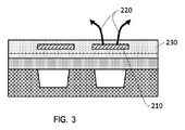
[0022] 図2は、図1の抵抗器および熱金属グラウンドに関する熱伝達経路200を例示する。図3は、熱金属グラウンドを用いない抵抗器210に関する熱伝達経路を例示する。熱金属領域120および熱ポスト(122a、122b)は、抵抗器が経験する熱インピーダンス(the thermal impedance seen by the resistors)を実質的に(例えば、25%)に低めることができる。定性的に(Qualitatively)、これは、図2に例示される熱伝達経路200を、図3に例示される熱伝達経路220と比較することによって、理解されることができる。熱金属グラウンドのない熱伝達経路220は、一般に、誘電体層(例えば、誘電体230および抵抗器の上方の他の誘電体層、あるいは、誘電体230および抵抗器の下方の他の誘電体層)を通したものである。熱金属グラウンドを有する熱伝達経路200は、一般に、金属およびシリコン層(例えば、熱ポスト(122a、122b)、熱金属領域120、コンタクト(150a、152a、150b、152b)、および基板140を通したものである。金属層およびシリコン基板は、良好な熱導体であり、誘電体層は不良熱導体であるので、よって金属および基板を通した熱経路は、誘電体を通した経路よりも抵抗が少ない(less resistive than)。
[0022] FIG. 2 illustrates a
[0023] 図4は、ここに開示された実施形態による、集積回路中の抵抗器から熱を散逸させるための方法を例示するフローチャートである。図4の処理は、様々な集積回路を用いて実行され得るが、具体的な例を提供するために、この方法は、図1を参照して説明される。 [0023] FIG. 4 is a flowchart illustrating a method for dissipating heat from a resistor in an integrated circuit according to embodiments disclosed herein. The process of FIG. 4 may be performed using a variety of integrated circuits, but to provide a specific example, the method will be described with reference to FIG.
[0024] ステップ410において、熱は、1つ以上の熱ポストを使用して、抵抗器から熱金属グラウンドへ伝導される。熱ポストは、熱金属グラウンドと抵抗器との間に配置される。例えば、熱は、熱ポスト122aを使用して、抵抗器110aから熱金属領域120へ伝導されることができる。
[0024] In
[0025] ステップ410において、熱は、熱金属グラウンドから集積回路の基板へ伝導される。例えば、熱は、コンタクト150b、152を使用して、熱金属領域120から基板140へ伝導されることができる。
[0025] In
[0026] 図4の処理は、例えば、追加、省略、並べ替え、または変更(altering)ステップによって修正され得る。加えて、複数のステップが同時に実行され得る。 [0026] The process of FIG. 4 may be modified by, for example, addition, omission, reordering, or altering steps. In addition, multiple steps can be performed simultaneously.
[0027] 本発明の実施形態は、特定の実施形態に関して上で説明されたが、例えば、異なる数の抵抗器、熱ポスト、および熱金属領域を用いる本発明の多くの変形が、可能性である。様々な要素の形および位置もまた変えられることができる。例示された実施形態では、熱金属領域が、抵抗器へ接続するためにも使用される第1の金属層に形成されるので、熱金属領域および抵抗器は部分的にのみオーバーラップする。他の実施形態は、異なる層を使用し得、熱金属領域と抵抗器との間の完全なオーバーラップを有し得る。 [0027] While embodiments of the present invention have been described above with respect to particular embodiments, many variations of the present invention, for example using different numbers of resistors, thermal posts, and thermal metal regions, are possible. is there. The shape and position of the various elements can also be changed. In the illustrated embodiment, the hot metal region and the resistor only partially overlap because the hot metal region is formed in the first metal layer that is also used to connect to the resistor. Other embodiments may use different layers and may have a complete overlap between the hot metal area and the resistor.
[0028] 上方、下方、左、右のような、方向を示す用語(terms)が、いくつかの特徴を説明するために使用されている。この専門用語(terminology)は、明確で簡潔な説明を提供するために使用されている。これら用語は、相対的なものであり、特定の絶対的な方向を暗示するものではない。加えて、様々な実施形態の特徴が、上述した組合せとは異なる組合せで組わせられ得る。 [0028] Directional terms, such as up, down, left, right, are used to describe some features. This terminology is used to provide a clear and concise explanation. These terms are relative and do not imply any particular absolute direction. In addition, the features of the various embodiments may be combined in combinations other than those described above.
[0029] 開示された実施形態の上記説明は、当業者が本発明を製造または使用することができるように提供されている。これらの実施形態への様々な修正は、当業者には容易に明らかであるだろうし、ここに説明された一般的な原理は、本発明の精神または範囲から逸脱しない限り他の実施形態にも適用可能であることができる。したがって、ここに提示された説明および図面は、本発明の現在好ましい実施形態を表し、よって、本発明により広く熟慮される主題事項を代表するものであることは理解されるべきである。さらに、本発明の範囲は、当業者に自明になり得る他の実施形態を完全に包含すること、および、本発明の範囲はしたがって、添付の特許請求の範囲以外の何によっても限定されないことは理解されるべきである。 [0029] The above description of the disclosed embodiments is provided to enable any person skilled in the art to make or use the present invention. Various modifications to these embodiments will be readily apparent to those skilled in the art, and the generic principles described herein may be practiced in other embodiments without departing from the spirit or scope of the invention. Can be applicable. Accordingly, it is to be understood that the description and drawings presented herein represent presently preferred embodiments of the invention and are therefore representative of subject matter that is widely contemplated by the present invention. Moreover, the scope of the present invention fully encompasses other embodiments that may be obvious to those skilled in the art, and the scope of the present invention is therefore not limited by anything other than the appended claims. Should be understood.
[0029] 開示された実施形態の上記説明は、当業者が本発明を製造または使用することができるように提供されている。これらの実施形態への様々な修正は、当業者には容易に明らかであるだろうし、ここに説明された一般的な原理は、本発明の精神または範囲から逸脱しない限り他の実施形態にも適用可能であることができる。したがって、ここに提示された説明および図面は、本発明の現在好ましい実施形態を表し、よって、本発明により広く熟慮される主題事項を代表するものであることは理解されるべきである。さらに、本発明の範囲は、当業者に自明になり得る他の実施形態を完全に包含すること、および、本発明の範囲はしたがって、添付の特許請求の範囲以外の何によっても限定されないことは理解されるべきである。
以下に本願の出願当初の特許請求の範囲に記載された発明を付記する。
[C1] 集積回路であって、
抵抗器と、
前記抵抗器の少なくとも一部に、オーバーラップし、かつ並行に配置された金属領域と、
前記金属領域に電気的に接続され、かつ前記金属領域と前記抵抗器との間に配置された1つ以上の熱ポストと、前記熱ポストは、前記抵抗器とは電気的に絶縁される、
を備える、集積回路。
[C2] 前記金属領域は、前記集積回路の基板に電気的に接続される、C1に記載の集積回路。
[C3] 前記抵抗器は、窒化チタンで形成される、C1に記載の集積回路。
[C4] 前記金属領域は、前記集積回路の第1の金属層に形成される、C1に記載の集積回路。
[C5] 前記金属領域は、前記抵抗器の上方に配置される、C1に記載の集積回路。
[C6] 前記抵抗器は、誘電体で囲まれる、C1に記載の集積回路。
[C7] 集積回路中の抵抗器から熱を散逸させるための方法であって、
熱金属グラウンドと前記抵抗器との間に配置された1つ以上の熱ポストを使用して、前記抵抗器から前記熱金属グラウンドへ熱を伝導することと、
前記熱金属グラウンドから前記集積回路の基板へ熱を伝導することと、
を備える、方法。
[C8] 前記熱金属グラウンドは、前記抵抗器の少なくとも一部にオーバーラップし、かつ並行に配置される、C7に記載の方法。
[C9] 前記熱ポストは、前記熱金属グラウンドに電気的に接続され、前記熱ポストは、前記抵抗器とは電気的に絶縁される、C7に記載の方法。
[C10] 前記熱金属グラウンドは、前記集積回路の前記基板に電気的に接続される、C7に記載の方法。
[C11] 前記抵抗器は、窒化チタンで形成される、C7に記載の方法。
[C12] 前記熱金属グラウンドは、前記集積回路の第1の金属層に形成される、C7に記載の方法。
[C13] 前記抵抗器は、誘電体で囲まれる、C7に記載の方法。
[C14] 集積回路であって、
抵抗器と、
前記抵抗器の少なくとも一部に、オーバーラップし、かつ並行に配置された金属領域と、
前記抵抗器から前記金属領域へ熱を伝導するための手段と、
を備える集積回路。
[C15] 前記熱を伝導するための手段は、前記金属領域に電気的に接続され、前記金属領域と前記抵抗器との間に配置された1つ以上の熱ポストを含み、前記熱ポストは、前記抵抗器とは電気的に絶縁される、C14に記載の集積回路。
[C16] 前記金属領域は、前記集積回路の基板に電気的に接続される、C14に記載の集積回路。
[C17] 前記抵抗器は、窒化チタンで形成される、C14に記載の集積回路。
[C18] 前記金属領域は、前記集積回路の第1の金属層に形成される、C14に記載の集積回路。
[C19] 前記金属領域は、前記抵抗器の上方に配置される、C14に記載の集積回路。
[C20] 前記抵抗器は、誘電体で囲まれる、C14に記載の集積回路。
[0029] The above description of the disclosed embodiments is provided to enable any person skilled in the art to make or use the present invention. Various modifications to these embodiments will be readily apparent to those skilled in the art, and the generic principles described herein may be practiced in other embodiments without departing from the spirit or scope of the invention. Can be applicable. Accordingly, it is to be understood that the description and drawings presented herein represent presently preferred embodiments of the invention and are therefore representative of subject matter that is widely contemplated by the present invention. Moreover, the scope of the present invention fully encompasses other embodiments that may be obvious to those skilled in the art, and the scope of the present invention is therefore not limited by anything other than the appended claims. Should be understood.
The invention described in the scope of claims at the beginning of the application of the present application will be added below.
[C1] an integrated circuit,
A resistor,
A metal region overlapping and arranged in parallel with at least a portion of the resistor;
One or more thermal posts electrically connected to the metal region and disposed between the metal region and the resistor, the thermal post being electrically insulated from the resistor;
An integrated circuit comprising:
[C2] The integrated circuit according to C1, wherein the metal region is electrically connected to a substrate of the integrated circuit.
[C3] The integrated circuit according to C1, wherein the resistor is formed of titanium nitride.
[C4] The integrated circuit according to C1, wherein the metal region is formed in a first metal layer of the integrated circuit.
[C5] The integrated circuit according to C1, wherein the metal region is disposed above the resistor.
[C6] The integrated circuit according to C1, wherein the resistor is surrounded by a dielectric.
[C7] A method for dissipating heat from a resistor in an integrated circuit comprising:
Conducting heat from the resistor to the hot metal ground using one or more thermal posts disposed between the hot metal ground and the resistor;
Conducting heat from the thermal metal ground to the substrate of the integrated circuit;
A method comprising:
[C8] The method of C7, wherein the thermal metal ground overlaps at least a portion of the resistor and is disposed in parallel.
[C9] The method of C7, wherein the thermal post is electrically connected to the thermal metal ground and the thermal post is electrically insulated from the resistor.
[C10] The method of C7, wherein the thermal metal ground is electrically connected to the substrate of the integrated circuit.
[C11] The method according to C7, wherein the resistor is formed of titanium nitride.
[C12] The method of C7, wherein the thermal metal ground is formed in a first metal layer of the integrated circuit.
[C13] The method of C7, wherein the resistor is surrounded by a dielectric.
[C14] an integrated circuit,
A resistor,
A metal region overlapping and arranged in parallel with at least a portion of the resistor;
Means for conducting heat from the resistor to the metal region;
An integrated circuit comprising:
[C15] The means for conducting heat includes one or more thermal posts electrically connected to the metal region and disposed between the metal region and the resistor, the thermal post comprising: The integrated circuit according to C14, wherein the integrated circuit is electrically insulated from the resistor.
[C16] The integrated circuit according to C14, wherein the metal region is electrically connected to a substrate of the integrated circuit.
[C17] The integrated circuit according to C14, wherein the resistor is formed of titanium nitride.
[C18] The integrated circuit according to C14, wherein the metal region is formed in a first metal layer of the integrated circuit.
[C19] The integrated circuit according to C14, wherein the metal region is disposed above the resistor.
[C20] The integrated circuit according to C14, wherein the resistor is surrounded by a dielectric.
Claims (20)
抵抗器と、
前記抵抗器の少なくとも一部に、オーバーラップし、かつ並行に配置された金属領域と、
前記金属領域に電気的に接続され、かつ前記金属領域と前記抵抗器との間に配置された1つ以上の熱ポストと、前記熱ポストは、前記抵抗器とは電気的に絶縁される、
を備える、集積回路。 An integrated circuit,
A resistor,
A metal region overlapping and arranged in parallel with at least a portion of the resistor;
One or more thermal posts electrically connected to the metal region and disposed between the metal region and the resistor, the thermal post being electrically insulated from the resistor;
An integrated circuit comprising:
熱金属グラウンドと前記抵抗器との間に配置された1つ以上の熱ポストを使用して、前記抵抗器から前記熱金属グラウンドへ熱を伝導することと、
前記熱金属グラウンドから前記集積回路の基板へ熱を伝導することと、
を備える、方法。 A method for dissipating heat from a resistor in an integrated circuit comprising:
Conducting heat from the resistor to the hot metal ground using one or more thermal posts disposed between the hot metal ground and the resistor;
Conducting heat from the thermal metal ground to the substrate of the integrated circuit;
A method comprising:
抵抗器と、
前記抵抗器の少なくとも一部に、オーバーラップし、かつ並行に配置された金属領域と、
前記抵抗器から前記金属領域へ熱を伝導するための手段と、
を備える集積回路。 An integrated circuit,
A resistor,
A metal region overlapping and arranged in parallel with at least a portion of the resistor;
Means for conducting heat from the resistor to the metal region;
An integrated circuit comprising:
Applications Claiming Priority (3)
| Application Number | Priority Date | Filing Date | Title |
|---|---|---|---|
| US14/181,187 | 2014-02-14 | ||
| US14/181,187 US9930769B2 (en) | 2014-02-14 | 2014-02-14 | Thermal metal ground for integrated circuit resistors |
| PCT/US2015/015041 WO2015123146A1 (en) | 2014-02-14 | 2015-02-09 | Thermal metal ground for integrated circuit resistors |
Publications (3)
| Publication Number | Publication Date |
|---|---|
| JP2017506433A true JP2017506433A (en) | 2017-03-02 |
| JP2017506433A5 JP2017506433A5 (en) | 2018-04-05 |
| JP6416272B2 JP6416272B2 (en) | 2018-10-31 |
Family
ID=52577981
Family Applications (1)
| Application Number | Title | Priority Date | Filing Date |
|---|---|---|---|
| JP2016551306A Active JP6416272B2 (en) | 2014-02-14 | 2015-02-09 | Thermal metal ground for integrated circuit resistors |
Country Status (7)
| Country | Link |
|---|---|
| US (1) | US9930769B2 (en) |
| EP (1) | EP3105785B1 (en) |
| JP (1) | JP6416272B2 (en) |
| KR (1) | KR101977674B1 (en) |
| CN (1) | CN105993071B (en) |
| BR (1) | BR112016018572B1 (en) |
| WO (1) | WO2015123146A1 (en) |
Families Citing this family (7)
| Publication number | Priority date | Publication date | Assignee | Title |
|---|---|---|---|---|
| CN106416433B (en) * | 2014-05-22 | 2019-03-08 | 松下知识产权经营株式会社 | Circuit substrate |
| US10304772B2 (en) * | 2017-05-19 | 2019-05-28 | Taiwan Semiconductor Manufacturing Co., Ltd. | Semiconductor device structure with resistive element |
| US10290676B2 (en) * | 2017-08-15 | 2019-05-14 | Northrop Grumman Systems Corporation | Superconducting device with thermally conductive heat sink |
| US10510637B2 (en) * | 2017-08-30 | 2019-12-17 | Taiwan Semiconductor Manufacturing Co., Ltd. | Devices and methods for heat dissipation of semiconductor integrated circuits |
| US10475725B2 (en) | 2017-11-08 | 2019-11-12 | Texas Instruments Incorporated | Structure to enable higher current density in integrated circuit resistor |
| US11522118B2 (en) | 2020-01-09 | 2022-12-06 | Northrop Grumman Systems Corporation | Superconductor structure with normal metal connection to a resistor and method of making the same |
| US11222849B2 (en) | 2020-04-24 | 2022-01-11 | Taiwan Semiconductor Manufacturing Company, Ltd. | Substrate loss reduction for semiconductor devices |
Citations (7)
| Publication number | Priority date | Publication date | Assignee | Title |
|---|---|---|---|---|
| JPH01214048A (en) * | 1988-02-23 | 1989-08-28 | Fujitsu Ltd | Semiconductor integrated device |
| JPH04249360A (en) * | 1991-02-05 | 1992-09-04 | Nec Ic Microcomput Syst Ltd | Semiconductor input protective circuit |
| JPH09252084A (en) * | 1996-03-15 | 1997-09-22 | Hitachi Ltd | Semiconductor resistor device |
| JP2000306998A (en) * | 1999-04-20 | 2000-11-02 | Nec Corp | Semiconductor device and its manufacture |
| JP2010177506A (en) * | 2009-01-30 | 2010-08-12 | Nec Corp | Wiring board, and method of manufacturing the same |
| WO2011001494A1 (en) * | 2009-06-29 | 2011-01-06 | 富士通株式会社 | Semiconductor device and manufacturing method thereof |
| JP2011249430A (en) * | 2010-05-24 | 2011-12-08 | Panasonic Corp | Semiconductor device and method for manufacturing the same |
Family Cites Families (15)
| Publication number | Priority date | Publication date | Assignee | Title |
|---|---|---|---|---|
| JPH04249340A (en) * | 1991-02-05 | 1992-09-04 | Canon Inc | Alignment method of semiconductor wafer |
| US6838372B2 (en) * | 2002-09-25 | 2005-01-04 | Cookson Electronics, Inc. | Via interconnect forming process and electronic component product thereof |
| US7345364B2 (en) | 2004-02-04 | 2008-03-18 | Agere Systems Inc. | Structure and method for improved heat conduction for semiconductor devices |
| US7310036B2 (en) | 2005-01-10 | 2007-12-18 | International Business Machines Corporation | Heat sink for integrated circuit devices |
| US7166913B2 (en) | 2005-04-19 | 2007-01-23 | International Business Machines Corporation | Heat dissipation for heat generating element of semiconductor device and related method |
| JP5005241B2 (en) * | 2006-03-23 | 2012-08-22 | ルネサスエレクトロニクス株式会社 | Semiconductor device and manufacturing method thereof |
| US8013394B2 (en) | 2007-03-28 | 2011-09-06 | International Business Machines Corporation | Integrated circuit having resistor between BEOL interconnect and FEOL structure and related method |
| US9111779B2 (en) | 2008-08-07 | 2015-08-18 | Texas Instruments Incorporated | IC resistor formed with integral heatsinking structure |
| US8048794B2 (en) * | 2009-08-18 | 2011-11-01 | International Business Machines Corporation | 3D silicon-silicon die stack structure and method for fine pitch interconnection and vertical heat transport |
| US8053870B2 (en) | 2009-12-15 | 2011-11-08 | International Business Machines Corporation | Semiconductor structure incorporating multiple nitride layers to improve thermal dissipation away from a device and a method of forming the structure |
| US8222745B2 (en) * | 2010-01-19 | 2012-07-17 | Lsi Corporation | Integrated heat sink |
| US8848374B2 (en) | 2010-06-30 | 2014-09-30 | Taiwan Semiconductor Manufacturing Company, Ltd. | Method and structure for dissipating heat away from a resistor having neighboring devices and interconnects |
| US8486796B2 (en) | 2010-11-19 | 2013-07-16 | International Business Machines Corporation | Thin film resistors and methods of manufacture |
| US8652922B2 (en) * | 2011-01-18 | 2014-02-18 | International Business Machines Corporation | Compact thermally controlled thin film resistors utilizing substrate contacts and methods of manufacture |
| US8530320B2 (en) * | 2011-06-08 | 2013-09-10 | International Business Machines Corporation | High-nitrogen content metal resistor and method of forming same |
-
2014
- 2014-02-14 US US14/181,187 patent/US9930769B2/en active Active
-
2015
- 2015-02-09 CN CN201580008191.9A patent/CN105993071B/en active Active
- 2015-02-09 EP EP15706331.4A patent/EP3105785B1/en active Active
- 2015-02-09 KR KR1020167024109A patent/KR101977674B1/en active IP Right Grant
- 2015-02-09 WO PCT/US2015/015041 patent/WO2015123146A1/en active Application Filing
- 2015-02-09 BR BR112016018572-2A patent/BR112016018572B1/en active IP Right Grant
- 2015-02-09 JP JP2016551306A patent/JP6416272B2/en active Active
Patent Citations (7)
| Publication number | Priority date | Publication date | Assignee | Title |
|---|---|---|---|---|
| JPH01214048A (en) * | 1988-02-23 | 1989-08-28 | Fujitsu Ltd | Semiconductor integrated device |
| JPH04249360A (en) * | 1991-02-05 | 1992-09-04 | Nec Ic Microcomput Syst Ltd | Semiconductor input protective circuit |
| JPH09252084A (en) * | 1996-03-15 | 1997-09-22 | Hitachi Ltd | Semiconductor resistor device |
| JP2000306998A (en) * | 1999-04-20 | 2000-11-02 | Nec Corp | Semiconductor device and its manufacture |
| JP2010177506A (en) * | 2009-01-30 | 2010-08-12 | Nec Corp | Wiring board, and method of manufacturing the same |
| WO2011001494A1 (en) * | 2009-06-29 | 2011-01-06 | 富士通株式会社 | Semiconductor device and manufacturing method thereof |
| JP2011249430A (en) * | 2010-05-24 | 2011-12-08 | Panasonic Corp | Semiconductor device and method for manufacturing the same |
Also Published As
| Publication number | Publication date |
|---|---|
| KR101977674B1 (en) | 2019-05-13 |
| KR20160122177A (en) | 2016-10-21 |
| WO2015123146A1 (en) | 2015-08-20 |
| CN105993071B (en) | 2019-11-29 |
| US20150237709A1 (en) | 2015-08-20 |
| BR112016018572A2 (en) | 2017-08-08 |
| JP6416272B2 (en) | 2018-10-31 |
| EP3105785A1 (en) | 2016-12-21 |
| BR112016018572B1 (en) | 2022-04-26 |
| US9930769B2 (en) | 2018-03-27 |
| CN105993071A (en) | 2016-10-05 |
| EP3105785B1 (en) | 2017-11-22 |
Similar Documents
| Publication | Publication Date | Title |
|---|---|---|
| JP6416272B2 (en) | Thermal metal ground for integrated circuit resistors | |
| US10643986B2 (en) | Power gating for three dimensional integrated circuits (3DIC) | |
| US7310036B2 (en) | Heat sink for integrated circuit devices | |
| TWI527169B (en) | Semiconductor device and method of manufacturing the same and fin field effect transistor | |
| TWI396254B (en) | Semiconductor device with local interconnects | |
| US8222745B2 (en) | Integrated heat sink | |
| JP5739123B2 (en) | Semiconductor structure and method of manufacturing the same | |
| US8482131B2 (en) | Via structure | |
| US20050250300A1 (en) | Low ohmic layout technique for MOS transistors | |
| TWI566401B (en) | Multiple fin finfet with low-resistance gate structure | |
| US9111934B2 (en) | Semiconductor device | |
| US7919830B2 (en) | Method and structure for ballast resistor | |
| TWI553821B (en) | Electrostatic discharge protection structure | |
| US7031163B2 (en) | Mechanical cooling fin for interconnects | |
| US20240014205A1 (en) | Input/output port circuit and chip thereof | |
| CN115458504A (en) | Semiconductor packaging structure and forming method thereof |
Legal Events
| Date | Code | Title | Description |
|---|---|---|---|
| A521 | Request for written amendment filed |
Free format text: JAPANESE INTERMEDIATE CODE: A523 Effective date: 20161026 Free format text: JAPANESE INTERMEDIATE CODE: A523 Effective date: 20161027 |
|
| A521 | Request for written amendment filed |
Free format text: JAPANESE INTERMEDIATE CODE: A523 Effective date: 20180112 |
|
| A621 | Written request for application examination |
Free format text: JAPANESE INTERMEDIATE CODE: A621 Effective date: 20180112 |
|
| A521 | Request for written amendment filed |
Free format text: JAPANESE INTERMEDIATE CODE: A523 Effective date: 20180220 |
|
| A871 | Explanation of circumstances concerning accelerated examination |
Free format text: JAPANESE INTERMEDIATE CODE: A871 Effective date: 20180220 |
|
| A975 | Report on accelerated examination |
Free format text: JAPANESE INTERMEDIATE CODE: A971005 Effective date: 20180620 |
|
| A131 | Notification of reasons for refusal |
Free format text: JAPANESE INTERMEDIATE CODE: A131 Effective date: 20180626 |
|
| A977 | Report on retrieval |
Free format text: JAPANESE INTERMEDIATE CODE: A971007 Effective date: 20180629 |
|
| A521 | Request for written amendment filed |
Free format text: JAPANESE INTERMEDIATE CODE: A523 Effective date: 20180808 |
|
| TRDD | Decision of grant or rejection written | ||
| A01 | Written decision to grant a patent or to grant a registration (utility model) |
Free format text: JAPANESE INTERMEDIATE CODE: A01 Effective date: 20180904 |
|
| A61 | First payment of annual fees (during grant procedure) |
Free format text: JAPANESE INTERMEDIATE CODE: A61 Effective date: 20181003 |
|
| R150 | Certificate of patent or registration of utility model |
Ref document number: 6416272 Country of ref document: JP Free format text: JAPANESE INTERMEDIATE CODE: R150 |
|
| R250 | Receipt of annual fees |
Free format text: JAPANESE INTERMEDIATE CODE: R250 |
|
| R250 | Receipt of annual fees |
Free format text: JAPANESE INTERMEDIATE CODE: R250 |
|
| R250 | Receipt of annual fees |
Free format text: JAPANESE INTERMEDIATE CODE: R250 |