JP2017504267A - Key extraction during secure boot - Google Patents
Key extraction during secure boot Download PDFInfo
- Publication number
- JP2017504267A JP2017504267A JP2016546025A JP2016546025A JP2017504267A JP 2017504267 A JP2017504267 A JP 2017504267A JP 2016546025 A JP2016546025 A JP 2016546025A JP 2016546025 A JP2016546025 A JP 2016546025A JP 2017504267 A JP2017504267 A JP 2017504267A
- Authority
- JP
- Japan
- Prior art keywords
- volatile memory
- secure
- memory circuit
- circuit
- logic state
- Prior art date
- Legal status (The legal status is an assumption and is not a legal conclusion. Google has not performed a legal analysis and makes no representation as to the accuracy of the status listed.)
- Pending
Links
Images


Classifications
-
- G—PHYSICS
- G06—COMPUTING; CALCULATING OR COUNTING
- G06F—ELECTRIC DIGITAL DATA PROCESSING
- G06F21/00—Security arrangements for protecting computers, components thereof, programs or data against unauthorised activity
- G06F21/50—Monitoring users, programs or devices to maintain the integrity of platforms, e.g. of processors, firmware or operating systems
- G06F21/57—Certifying or maintaining trusted computer platforms, e.g. secure boots or power-downs, version controls, system software checks, secure updates or assessing vulnerabilities
- G06F21/575—Secure boot
-
- H—ELECTRICITY
- H04—ELECTRIC COMMUNICATION TECHNIQUE
- H04L—TRANSMISSION OF DIGITAL INFORMATION, e.g. TELEGRAPHIC COMMUNICATION
- H04L9/00—Cryptographic mechanisms or cryptographic arrangements for secret or secure communications; Network security protocols
- H04L9/08—Key distribution or management, e.g. generation, sharing or updating, of cryptographic keys or passwords
- H04L9/0861—Generation of secret information including derivation or calculation of cryptographic keys or passwords
- H04L9/0866—Generation of secret information including derivation or calculation of cryptographic keys or passwords involving user or device identifiers, e.g. serial number, physical or biometrical information, DNA, hand-signature or measurable physical characteristics
-
- H—ELECTRICITY
- H04—ELECTRIC COMMUNICATION TECHNIQUE
- H04L—TRANSMISSION OF DIGITAL INFORMATION, e.g. TELEGRAPHIC COMMUNICATION
- H04L9/00—Cryptographic mechanisms or cryptographic arrangements for secret or secure communications; Network security protocols
- H04L9/08—Key distribution or management, e.g. generation, sharing or updating, of cryptographic keys or passwords
- H04L9/0894—Escrow, recovery or storing of secret information, e.g. secret key escrow or cryptographic key storage
Abstract
1つの特徴は、集積回路のセキュアブートフロー中に秘密鍵を抽出するための方法に関する。詳細には、セキュアブートフローは、複数の初期論理状態値を生成するために第1の揮発性メモリ回路を電源投入することと、複数の初期論理状態値に基づいて秘密データを導出することと、セキュア実行環境(SEE)によってセキュアにされるセキュア揮発性メモリ回路中に秘密データを記憶することと、第1の揮発性メモリ回路中の複数の初期論理状態値をクリアすることと、秘密データに基づいて秘密鍵を抽出するためにSEEにおいて暗号アルゴリズムを実行することと、セキュア揮発性メモリ回路中に秘密鍵を記憶することとを含む。セキュアブートフローは、非セキュアアプリケーションから秘密データと複数の初期論理状態値とをセキュアにするために第1の揮発性メモリ回路へのアクセスを制御する。One feature relates to a method for extracting a secret key during a secure boot flow of an integrated circuit. Specifically, the secure boot flow powers on the first volatile memory circuit to generate a plurality of initial logic state values and derives secret data based on the plurality of initial logic state values. Storing secret data in a secure volatile memory circuit secured by a secure execution environment (SEE), clearing multiple initial logic state values in the first volatile memory circuit, and secret data Executing a cryptographic algorithm in the SEE to extract a secret key based on the sigma and storing the secret key in a secure volatile memory circuit. The secure boot flow controls access to the first volatile memory circuit to secure secret data and a plurality of initial logical state values from a non-secure application.
Description
関連出願の相互参照
本出願は、内容全体が参照によって本明細書に組み込まれる、2014年1月22日に米国特許商標庁に出願された、米国非仮特許出願第14/161,185号の優先権および利益を主張する。
CROSS REFERENCE TO RELATED APPLICATIONS This application is a priority of US Non-Provisional Patent Application No. 14 / 161,185 filed with the US Patent and Trademark Office on January 22, 2014, the entire contents of which are incorporated herein by reference. And insist on profit.
様々な特徴は、概して、セキュア暗号鍵抽出および記憶に関し、より詳細には、揮発性メモリの物理的クローン不能特徴に基づいてセキュアブートプロセス中に秘密暗号鍵を抽出し、記憶することに関する。 Various features generally relate to secure encryption key extraction and storage, and more particularly to extracting and storing a secret encryption key during a secure boot process based on the physical non-clonal characteristics of volatile memory.
モバイルフォン、タブレット、およびコンピュータなど多くの電子通信デバイスは、電子通信デバイスにおいて暗号セキュリティプロセスのために使用され得るデバイス固有の暗号鍵(またはそのような鍵から導出された鍵)を含む。たとえば、デバイスと、場合によっては、別の信頼できるエンティティ(たとえば、デバイスに通信サービスを提供するセルラーネットワーク認証サーバ)とにのみ知られているデバイス固有鍵が、デバイスによって送信された通信メッセージを暗号化するためにその後使用される鍵(たとえば、公開鍵と秘密鍵とのペア)を導出するために使用される。他の当事者および/またはアプリケーションによる無許可のアクセスからデバイス固有鍵をセキュアにすることは、デバイスおよび/または通信ネットワークによって採用される暗号化セキュリティプロトコルの完全性をより良く保証するために最も重要である。 Many electronic communication devices such as mobile phones, tablets, and computers include device-specific cryptographic keys (or keys derived from such keys) that can be used for cryptographic security processes in electronic communication devices. For example, a device-specific key known only to the device and possibly another trusted entity (for example, a cellular network authentication server that provides communication services to the device) encrypts communication messages sent by the device. Used to derive a key (eg, a public and private key pair) that is subsequently used to Securing device-specific keys from unauthorized access by other parties and / or applications is most important to better ensure the integrity of cryptographic security protocols employed by devices and / or communication networks. is there.
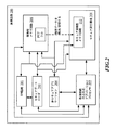
図1に、電子通信デバイスにおいて見つけられ得る従来技術の集積回路(IC)100の概略ブロック図を示す。IC100は、ブートローダ102と、ユーザアプリケーション104と、不揮発性メモリ回路106とを含み、次に、不揮発性メモリ回路106は、IC100を有するデバイスに一意であり得る暗号鍵108を記憶する。IC100が電源投入されると、IC100は、IC100の様々な態様を初期化するブートローダを取り出し、実行する。IC100がそれ自体のブートアッププロセスを完了した後、ユーザアプリケーション104(たとえば、高レベルオペレーティングシステム(HLOS)、そのようなHLOS上で実行されるアプリケーションなど)が実行され得る。ブートローダ102およびユーザアプリケーション104は、鍵108への直接アクセスを有し得る。たとえば、ユーザアプリケーションは、不揮発性メモリ106から鍵108を取り出し、鍵108を暗号化プロセスのために使用される追加の鍵を導出するために使用し得る。
FIG. 1 shows a schematic block diagram of a prior art integrated circuit (IC) 100 that may be found in an electronic communication device. The IC 100 includes a
さらに、鍵108を記憶するメモリ回路106が不揮発性メモリであるので、鍵108は、IC100が電源切断または電源投入されたかどうかにかかわらずIC100中に記憶される(したがって、理論的にはアクセス可能である)。これは、鍵108をより大きいセキュリティ脆弱性にさらす。たとえば、集積回路100パッケージの上部は、物理的に開かれ得、電子顕微鏡が、鍵108を記憶するために使用される回路(たとえば、ヒューズ)を分析するために使用され得る。そうすることは、鍵108を明らかにし、デバイスのセキュリティを損ない得る。
In addition, since the
そのような鍵への無許可のアクセスを防ぐのを助ける鍵の抽出/生成および記憶におけるセキュリティを増大する方法および装置が必要である。キー抽出/生成および記憶におけるセキュリティの改善は、そのような鍵に依拠する暗号アルゴリズムおよびプロセスに対する信頼度および信頼性を増加させるのを助ける。 There is a need for a method and apparatus that increases security in key extraction / generation and storage that helps prevent unauthorized access to such keys. Improved security in key extraction / generation and storage helps increase the confidence and reliability of cryptographic algorithms and processes that rely on such keys.
1つの特徴は、集積回路において動作可能な方法であって、複数の初期論理状態値を生成するために第1の揮発性メモリ回路を電源投入するステップであって、第1の揮発性メモリ回路が集積回路上にある、ステップと、複数の初期論理状態値に基づいて秘密データを導出するステップと、セキュア揮発性メモリ回路中に秘密データを記憶するステップであって、セキュア揮発性メモリ回路が、セキュア実行環境(SEE)によってセキュアにされる、ステップと、第1の揮発性メモリ回路中の複数の初期論理状態値をクリアするステップと、秘密データに基づいて秘密鍵を抽出するためにSEEにおいて暗号アルゴリズムを実行するステップと、セキュア揮発性メモリ回路中に秘密鍵を記憶するステップとを含む方法を提供する。一態様によれば、本方法は、1つまたは複数の非セキュアアプリケーションから秘密データと複数の初期論理状態値とをセキュアにするために、第1の揮発性メモリ回路へのアクセスを制御する集積回路のセキュアブートフローである。別の態様によれば、セキュアブートフローは、少なくとも複数の初期論理状態値が第1の揮発性メモリ回路中でクリアされるまで第1の揮発性メモリ回路を1つまたは複数の非セキュアアプリケーションからアクセス不可能にすることによって、1つまたは複数の非セキュアアプリケーションから秘密データと複数の初期論理状態値とをセキュアにする。 One feature is a method operable in an integrated circuit, the step of powering up the first volatile memory circuit to generate a plurality of initial logic state values, the first volatile memory circuit On the integrated circuit, deriving secret data based on a plurality of initial logic state values, and storing the secret data in the secure volatile memory circuit, the secure volatile memory circuit comprising: Secured by a secure execution environment (SEE), clearing a plurality of initial logical state values in the first volatile memory circuit, and extracting a secret key based on the secret data A method is provided that includes executing a cryptographic algorithm at, and storing a secret key in a secure volatile memory circuit. According to one aspect, the method includes an integrated control that controls access to the first volatile memory circuit to secure secret data and a plurality of initial logic state values from one or more non-secure applications. This is a secure boot flow of the circuit. According to another aspect, the secure boot flow includes removing the first volatile memory circuit from one or more non-secure applications until at least a plurality of initial logic state values are cleared in the first volatile memory circuit. By making inaccessible, secret data and multiple initial logical state values are secured from one or more non-secure applications.
一態様によれば、セキュアブートフローは、1次ブートローダと、第1の2次ブートローダと、第2の2次ブートローダとを含み、セキュアブートフローは、第1の2次ブートローダが実行する前に1次ブートローダに第1の2次ブートローダを認証させることによって信用チェーンを確立し、第1の2次ブートローダは、第2の2次ブートローダが実行する前に第2の2次ブートローダを認証し、第2の2次ブートローダがSEEを認証し、秘密鍵は、セキュアブートフロー中に、および1つまたは複数の非セキュアアプリケーションの実行より前に、抽出され、セキュア揮発性メモリ回路中に記憶される。別の態様によれば、第1の揮発性メモリ回路がリセットされると、セキュアブートフローが実行される。さらに別の態様によれば、秘密データは、複数の初期論理状態値である。 According to one aspect, the secure boot flow includes a primary boot loader, a first secondary boot loader, and a second secondary boot loader, the secure boot flow before the first secondary boot loader executes Establishing a trust chain by having the primary boot loader authenticate the first secondary boot loader, the first secondary boot loader authenticates the second secondary boot loader before the second secondary boot loader executes, A second secondary boot loader authenticates the SEE and the private key is extracted and stored in a secure volatile memory circuit during the secure boot flow and prior to execution of one or more non-secure applications . According to another aspect, the secure boot flow is executed when the first volatile memory circuit is reset. According to yet another aspect, the secret data is a plurality of initial logic state values.
一態様によれば、第1の揮発性メモリ回路をクリアした後に、第1の揮発性メモリ回路は、1つまたは複数の非セキュアアプリケーションのためのデータストレージのために利用可能になる。別の態様によれば、第1の揮発性メモリ回路は、スタティックランダムアクセスメモリ(SRAM)である。さらに別の態様によれば、SEEは、非セキュアアプリケーションがセキュア揮発性メモリ回路にアクセスするのを防ぐ。 According to one aspect, after clearing the first volatile memory circuit, the first volatile memory circuit becomes available for data storage for one or more non-secure applications. According to another aspect, the first volatile memory circuit is a static random access memory (SRAM). According to yet another aspect, SEE prevents non-secure applications from accessing secure volatile memory circuitry.
一態様によれば、複数の初期論理状態値は、第1の揮発性メモリ回路が電源投入されるたびに実質的に同じになる。別の態様によれば、暗号アルゴリズムは、ブロックコードアルゴリズム、拡散コードアルゴリズム、および/またはリピートコードアルゴリズムのうちの少なくとも1つに基づく。さらに別の態様によれば、本方法は、セキュア揮発性メモリ回路中に秘密データを記憶するより前に第2の揮発性メモリ回路中に秘密データを記憶するステップと、セキュア揮発性メモリ回路中に秘密データを記憶した後に第2の揮発性メモリ回路中に記憶された秘密データをクリアするステップとをさらに含む。 According to one aspect, the plurality of initial logic state values are substantially the same each time the first volatile memory circuit is powered on. According to another aspect, the cryptographic algorithm is based on at least one of a block code algorithm, a spreading code algorithm, and / or a repeat code algorithm. According to yet another aspect, the method includes storing the secret data in the second volatile memory circuit prior to storing the secret data in the secure volatile memory circuit; And clearing the secret data stored in the second volatile memory circuit after storing the secret data.
一態様によれば、第2の揮発性メモリ回路中に記憶された秘密データをクリアした後に、第2の揮発性メモリ回路が、1つまたは複数の非セキュアアプリケーションのためのデータストレージのために利用可能になる。別の態様によれば、SEEは、秘密鍵を非セキュアアプリケーションからアクセス不可能にすることによって秘密鍵へのアクセスを制御し、本方法は、副鍵および/または公開データのうちの少なくとも1つについてSEEにおいて非セキュアアプリケーションから要求を受信するステップと、秘密鍵に基づいてSEEにおいて副鍵および/または公開データを生成するステップと、副鍵および/または公開データを要求する非セキュアアプリケーションに副鍵および/または公開データを与えるステップとをさらに含む。さらに別の態様によれば、副鍵および/または公開データは、秘密鍵と、非セキュアアプリケーションによって与えられる他のデータとに基づいて生成される。別の態様によれば、秘密データに基づいて秘密鍵を抽出するためにSEEにおいて実行される暗号アルゴリズムは、不揮発性メモリ回路中に記憶された補助データにさらに基づく。 According to one aspect, after clearing the secret data stored in the second volatile memory circuit, the second volatile memory circuit is for data storage for one or more non-secure applications. Become available. According to another aspect, the SEE controls access to the secret key by making the secret key inaccessible from non-secure applications, and the method includes at least one of the subkey and / or public data. Receiving a request from the non-secure application at SEE, generating a sub-key and / or public data at SEE based on the private key, and a sub-key to the non-secure application requesting the sub-key and / or public data And / or providing public data. According to yet another aspect, the subkey and / or public data is generated based on the secret key and other data provided by the non-secure application. According to another aspect, the cryptographic algorithm executed in the SEE to extract the secret key based on the secret data is further based on auxiliary data stored in the non-volatile memory circuit.
別の特徴は、集積回路であって、電源投入時に複数の初期論理状態値を生成するように構成された第1の揮発性メモリ回路と、セキュア実行環境(SEE)によってセキュアにされるセキュア揮発性メモリ回路と、第1の揮発性メモリ回路とセキュア揮発性メモリ回路とに通信可能に結合された処理回路であって、複数の初期論理状態値に基づいて秘密データを導出することと、セキュア揮発性メモリ回路中に秘密データを記憶することと、第1の揮発性メモリ回路中の複数の初期論理状態値をクリアすることと、秘密データに基づいて秘密鍵を抽出するためにSEEにおいて暗号アルゴリズムを実行することと、セキュア揮発性メモリ回路中に秘密鍵を記憶することとを行うように構成された処理回路とを含む集積回路を提供する。一態様によれば、処理回路は、(i)秘密データを導出することと、(ii)秘密データを記憶することと、(iii)複数の初期論理状態値をクリアすることと、(iv)暗号アルゴリズムを実行することと、(v)秘密鍵を記憶することとを行うことによってセキュアブートフローを実行し、セキュアブートフローは、1つまたは複数の非セキュアアプリケーションから秘密データと複数の初期論理状態値とをセキュアにするために、第1の揮発性メモリ回路へのアクセスを制御する。 Another feature is an integrated circuit, a first volatile memory circuit configured to generate multiple initial logic state values upon power-up, and a secure volatile secured by a secure execution environment (SEE). A processing circuit communicatively coupled to the volatile memory circuit, the first volatile memory circuit, and the secure volatile memory circuit, wherein the secret data is derived based on the plurality of initial logic state values; Storing secret data in the volatile memory circuit, clearing multiple initial logic state values in the first volatile memory circuit, and encrypting in the SEE to extract the secret key based on the secret data An integrated circuit is provided that includes a processing circuit configured to execute an algorithm and store a secret key in a secure volatile memory circuit. According to one aspect, the processing circuit includes (i) deriving secret data, (ii) storing secret data, (iii) clearing a plurality of initial logic state values, and (iv) A secure boot flow is performed by executing a cryptographic algorithm and (v) storing a secret key, wherein the secure boot flow includes secret data and a plurality of initial logic from one or more non-secure applications. In order to secure the status value, access to the first volatile memory circuit is controlled.
一態様によれば、本処理回路は、セキュア揮発性メモリ回路中に秘密データを記憶するより前に第2の揮発性メモリ回路中に秘密データを記憶することと、セキュア揮発性メモリ回路中に秘密データを記憶した後に第2の揮発性メモリ回路中に記憶された秘密データをクリアすることとを行うようにさらに構成される。別の態様によれば、SEEは、秘密鍵を非セキュアアプリケーションからアクセス不可能にすることによって秘密鍵へのアクセスを制御し、本処理回路は、副鍵および/または公開データのうちの少なくとも1つについてSEEにおいて非セキュアアプリケーションから要求を受信することと、秘密鍵に基づいてSEEにおいて副鍵および/または公開データを生成することと、副鍵および/または公開データを要求する非セキュアアプリケーションに副鍵および/または公開データを与えることとを行うようにさらに構成される。 According to one aspect, the processing circuit stores the secret data in the second volatile memory circuit prior to storing the secret data in the secure volatile memory circuit; And further configured to clear the secret data stored in the second volatile memory circuit after storing the secret data. According to another aspect, the SEE controls access to the secret key by making the secret key inaccessible from a non-secure application, and the processing circuit includes at least one of the subkey and / or public data. Receiving a request from the non-secure application at the SEE, generating a sub-key and / or public data at the SEE based on the private key, and sub-sending to the non-secure application requesting the sub-key and / or public data. Is further configured to provide keys and / or public data.
別の特徴は、集積回路であって、複数の初期論理状態値を生成するために第1の揮発性メモリ回路を電源投入するための手段であって、第1の揮発性メモリ回路が集積回路上にある、手段と、複数の初期論理状態値に基づいて秘密データを導出するための手段と、セキュア揮発性メモリ回路中に秘密データを記憶するための手段であって、セキュア揮発性メモリ回路が、セキュア実行環境(SEE)によってセキュアにされる、手段と、第1の揮発性メモリ回路中の複数の初期論理状態値をクリアするための手段と、秘密データに基づいて秘密鍵を抽出するためにSEEにおいて暗号アルゴリズムを実行するための手段と、セキュア揮発性メモリ回路中に秘密鍵を記憶するための手段とを含む集積回路を提供する。 Another feature is an integrated circuit, means for powering on a first volatile memory circuit to generate a plurality of initial logic state values, the first volatile memory circuit being integrated circuit Means above, means for deriving secret data based on a plurality of initial logic state values, means for storing secret data in a secure volatile memory circuit, the secure volatile memory circuit Is secured by a secure execution environment (SEE), means for clearing a plurality of initial logical state values in the first volatile memory circuit, and extracts a secret key based on the secret data An integrated circuit is provided that includes means for executing a cryptographic algorithm in SEE and means for storing a secret key in a secure volatile memory circuit.
別の特徴は、1つまたは複数の命令を記憶したコンピュータ可読記憶媒体であって、命令は、少なくとも1つの集積回路によって実行されたとき、集積回路に、複数の初期論理状態値を生成するために第1の揮発性メモリ回路を電源投入することであって、第1の揮発性メモリ回路が集積回路上にある、電源投入することと、複数の初期論理状態値に基づいて秘密データを導出することと、セキュア揮発性メモリ回路中に秘密データを記憶することであって、セキュア揮発性メモリ回路が、セキュア実行環境(SEE)によってセキュアにされる、記憶することと、第1の揮発性メモリ回路中の複数の初期論理状態値をクリアすることと、秘密データに基づいて秘密鍵を抽出するためにSEEにおいて暗号アルゴリズムを実行することと、セキュア揮発性メモリ回路中に秘密鍵を記憶することとを行わせるコンピュータ可読記憶媒体を提供する。一態様によれば、1つまたは複数の命令は、集積回路のセキュアブートフローのためのものであり、命令は、集積回路によって実行されたとき、少なくとも複数の初期論理状態値が第1の揮発性メモリ回路中でクリアされるまで第1の揮発性メモリ回路を1つまたは複数の非セキュアアプリケーションからアクセス不可能にすることによって、1つまたは複数の非セキュアアプリケーションから秘密データと複数の初期論理状態値とをセキュアにするように第1の揮発性メモリ回路へのアクセスを制御する。 Another feature is a computer-readable storage medium having stored thereon one or more instructions for generating a plurality of initial logic state values in the integrated circuit when executed by at least one integrated circuit. The first volatile memory circuit is powered on, the first volatile memory circuit is on the integrated circuit, and the secret data is derived based on power-up and multiple initial logic state values Storing secret data in a secure volatile memory circuit, wherein the secure volatile memory circuit is secured by a secure execution environment (SEE) and storing the first volatile Clearing multiple initial logic state values in the memory circuit, executing a cryptographic algorithm in the SEE to extract a secret key based on the secret data, and a secure volatile memory A computer readable storage medium is provided for storing a secret key in a circuit. According to one aspect, the one or more instructions are for a secure boot flow of the integrated circuit, and when the instructions are executed by the integrated circuit, at least a plurality of initial logic state values are the first volatile. Secret data and multiple initial logic from one or more non-secure applications by making the first volatile memory circuit inaccessible to one or more non-secure applications until cleared in the volatile memory circuit Control access to the first volatile memory circuit to secure the state value.
以下の説明では、本開示の様々な態様を完全に理解することが可能なように具体的な詳細を示す。しかしながら、それらの態様が、これらの具体的な詳細なしに実施できることが、当業者には理解されよう。たとえば、態様を不必要に詳しく説明して曖昧にすることを避けるために、回路がブロック図で示される場合がある。他の例では、本開示の態様を曖昧にしないように、周知の回路、構造、および技術は詳細には示されていない場合がある。 In the following description, specific details are set forth to provide a thorough understanding of various aspects of the disclosure. However, those skilled in the art will appreciate that the embodiments can be practiced without these specific details. For example, circuitry may be shown in block diagram form in order to avoid unnecessarily elaborating and obscuring aspects. In other instances, well-known circuits, structures, and techniques may not be shown in detail in order not to obscure aspects of the present disclosure.
「例示的」という言葉は、「例、事例、または例示として役立つ」ことを意味するように本明細書において使用される。「例示的な」として本明細書において説明するいかなる実装形態または態様も、必ずしも本開示の他の態様よりも好ましいか、または有利であると解釈されるべきではない。同様に、「態様」という用語は、本開示のすべての態様が、説明された特徴、利点、または動作モードを含むことを必要としない。 The word “exemplary” is used herein to mean “serving as an example, instance, or illustration.” Any implementation or aspect described herein as "exemplary" is not necessarily to be construed as preferred or advantageous over other aspects of the disclosure. Similarly, the term “aspect” does not require that all aspects of the disclosure include the described features, advantages, or modes of operation.
概要
本明細書では、集積回路のセキュアブートフロー中に秘密鍵を抽出する方法および装置について説明する。詳細には、セキュアブートフローは、複数の初期論理状態値を生成するために第1の揮発性メモリ回路を電源投入することと、複数の初期論理状態値に基づいて秘密データを導出することと、セキュア実行環境(SEE)によってセキュアにされるセキュア揮発性メモリ回路中に秘密データを記憶することと、第1の揮発性メモリ回路中の複数の初期論理状態値をクリアすることと、秘密データに基づいて秘密鍵を抽出するためにSEEにおいて暗号アルゴリズムを実行することと、セキュア揮発性メモリ回路中に秘密鍵を記憶することとを含む。セキュアブートフローは、少なくとも複数の初期論理状態値が第1の揮発性メモリ回路中でクリアされるまで第1の揮発性メモリ回路を非セキュアアプリケーションからアクセス不可能にすることによって、非セキュアアプリケーションから秘密データと複数の初期論理状態値とをセキュアにするように第1の揮発性メモリ回路へのアクセスを制御する。さらに、第1の揮発性メモリ回路がリセットされる場合、セキュアブートフローが再び開始され、したがって、第1の揮発性メモリ回路の初期論理状態値は、非セキュアアプリケーションにとって利用不可能になる。
Overview This specification describes a method and apparatus for extracting a secret key during a secure boot flow of an integrated circuit. Specifically, the secure boot flow powers on the first volatile memory circuit to generate a plurality of initial logic state values and derives secret data based on the plurality of initial logic state values. Storing secret data in a secure volatile memory circuit secured by a secure execution environment (SEE), clearing multiple initial logic state values in the first volatile memory circuit, and secret data Executing a cryptographic algorithm in the SEE to extract a secret key based on the sigma and storing the secret key in a secure volatile memory circuit. The secure boot flow is a non-secure application that makes the first volatile memory circuit inaccessible from the non-secure application until at least a plurality of initial logic state values are cleared in the first volatile memory circuit. Access to the first volatile memory circuit is controlled to secure the secret data and the plurality of initial logical state values. Further, when the first volatile memory circuit is reset, the secure boot flow is started again, and therefore the initial logical state value of the first volatile memory circuit is not available for non-secure applications.
ICセキュアブートアップ中の例示的なキー抽出
図2に、本開示の一態様による集積回路(IC)200の高レベルの概略ブロック図を示す。IC200は、たとえば、処理回路、メモリ回路などを含むプロセッサであり得、限定はしないが、モバイルフォン、コンピュータ、タブレット、時計などの電子通信デバイスにおいて見つけられ得る。IC200は、リソース電力管理(RPM)回路201と、セキュアブートローダ回路202と、処理回路203と、非セキュアアプリケーション204と、揮発性メモリ回路206と、セキュア実行環境(SEE)208とを含み得る。揮発性メモリ回路206は、物理的クローン不能関数(PUF)210を含み、SEE208は、セキュア揮発性メモリ回路212を含む。
Exemplary Key Extraction During IC Secure Bootup FIG. 2 shows a high level schematic block diagram of an integrated circuit (IC) 200 according to one aspect of the present disclosure. IC 200 can be, for example, a processor including processing circuitry, memory circuitry, etc., and can be found in electronic communication devices such as, but not limited to, mobile phones, computers, tablets, watches. The IC 200 may include a resource power management (RPM)
特に、RPM回路201は、IC200の様々な回路および構成要素に電力を供給する。たとえば、RPM回路201は、処理回路203、揮発性メモリ回路206、および/またはセキュア揮発性メモリ回路212に供給される電力を制御し得る。RPM回路201は、複数の初期論理状態値を生成するために第1の揮発性メモリ回路を電源投入するための手段の一例を表す。
In particular, the
IC200の電源投入時に、IC200は、処理回路203にセキュアブートローダ(たとえば、セキュアブートコード)202を取得させ、実行させることによって、セキュアブートアッププロセス(本明細書では「セキュアブートフロー」とも呼ばれる)を行う/実行する。セキュアブートローダ202は、限定はしないが、読取り専用メモリ(ROM)および/または他の不揮発性メモリなどのメモリ回路中に記憶され得る。セキュアブートローダ202は、通常動作に向けてIC200を準備するために、IC200の様々なモジュールを初期化し、他の基本動作を実行する。 When the IC 200 is powered on, the IC 200 causes the processing circuit 203 to acquire and execute a secure boot loader (e.g., secure boot code) 202 to execute a secure boot up process (also referred to herein as a “secure boot flow”). Do / execute. Secure boot loader 202 may be stored in a memory circuit such as, but not limited to, read only memory (ROM) and / or other non-volatile memory. Secure boot loader 202 initializes various modules of IC 200 and performs other basic operations to prepare IC 200 for normal operation.
本開示の一態様によれば、揮発性メモリ回路206は、各々が複数のSRAM回路セルを含む1つまたは複数のスタティックランダムアクセスメモリ(SRAM)回路を含む。他の態様によれば、揮発性メモリ回路206は、SRAMに限定されず、埋込みダイナミックランダムアクセスメモリ(eDRAM)などの他のタイプの揮発性メモリに基づき得る。揮発性メモリ回路206の一部分(すなわち、いくつかの揮発性メモリセル)は、物理的クローン不能関数(PUF)の基礎を形成し得る。 According to one aspect of the present disclosure, the volatile memory circuit 206 includes one or more static random access memory (SRAM) circuits, each including a plurality of SRAM circuit cells. According to other aspects, the volatile memory circuit 206 is not limited to SRAM, but may be based on other types of volatile memory, such as embedded dynamic random access memory (eDRAM). A portion of volatile memory circuit 206 (ie, some volatile memory cells) may form the basis of a physical non-clonal function (PUF).
オンチップPUFは、集積回路(IC)の製造プロセスばらつきを活用するチップ固有のチャレンジレスポンス機構である。物理的刺激(すなわち、チャレンジ)がPUFに適用されると、PUFは、PUFを採用するデバイスの物理的微細構造との刺激の複雑な対話により予測不可能であるが繰り返し可能な方法でレスポンスを生成する。この厳密な微細構造は、PUFを採用するデバイスの製造中にもたらされる物理的要因に依存し、これは、予測不可能である。PUFの「クローン不能」は、1つのデバイスが別の、一見すると同一のデバイスと同じプロセスで製造される場合でも、PUFを採用する各デバイスが、チャレンジをレスポンスにマッピングする一意の予測不可能な方法を有することを意味する。したがって、製造プロセスの厳密な制御は実現不可能であるので、別のデバイスのPUFと同じチャレンジレスポンス挙動をもつPUFを構築することは実際に実現不可能である。 The on-chip PUF is a chip-specific challenge response mechanism that takes advantage of variations in the manufacturing process of integrated circuits (ICs). When a physical stimulus (i.e., a challenge) is applied to a PUF, the PUF responds in an unpredictable but repeatable manner due to the complex interaction of the stimulus with the physical microstructure of the device employing the PUF. Generate. This exact microstructure depends on the physical factors introduced during the manufacture of devices that employ PUF, which is unpredictable. PUF “non-cloneable” is a unique, unpredictable feature where each device adopting PUF maps a challenge to a response, even if one device is manufactured in the same process as another, seemingly identical device. Means to have a method. Therefore, since strict control of the manufacturing process is not feasible, it is actually impossible to construct a PUF having the same challenge-response behavior as the PUF of another device.
本開示では、揮発性メモリ回路206は、揮発性メモリ(たとえば、SRAM)の一種であり、ここで、揮発性メモリ回路206を含む各回路セルは、起動時に(すなわち、電源投入されたときに)初期の好適な論理状態値(たとえば、「0」または「1」)に自然に初期化する。たとえば、SRAMは、電源投入されたときに、そのような特性を有する。各揮発性メモリセルが、高確率で起動時に毎回同じ値に初期化するので、回路セルの初期論理状態値は繰り返し可能である。しかしながら、回路セルの初期論理状態値は、同じになるように製造された場合でも、ICごとにランダムになる。したがって、製造プロセスばらつきにより、各集積回路の揮発性メモリ回路206は、同じになるように製造された場合でも、異なる繰り返し可能な初期値を示すことになり、したがって、ICごとに、初期揮発性メモリ回路開始値が、異なるICにわたる同じメモリアドレスロケーションにおいて異なる。したがって、各IC200は、その揮発性メモリ回路のセルの初期電力オン状態に基づいて一意だが繰り返し可能な識別子を有する揮発性メモリ回路206(たとえば、SRAM回路)を有する。 In the present disclosure, volatile memory circuit 206 is a type of volatile memory (e.g., SRAM), where each circuit cell including volatile memory circuit 206 is turned on at startup (i.e., when powered on). ) Naturally initialize to the initial preferred logic state value (eg, “0” or “1”). For example, SRAM has such characteristics when powered on. Since each volatile memory cell is initialized to the same value each time at startup with high probability, the initial logic state value of the circuit cell is repeatable. However, even if the initial logic state values of the circuit cells are manufactured to be the same, they are random for each IC. Therefore, due to manufacturing process variations, the volatile memory circuit 206 of each integrated circuit will exhibit different repeatable initial values even when manufactured to be the same, and therefore, for each IC, the initial volatile Memory circuit start values are different at the same memory address location across different ICs. Thus, each IC 200 has a volatile memory circuit 206 (eg, an SRAM circuit) that has a unique but repeatable identifier based on the initial power-on state of the cells of that volatile memory circuit.
PUF210のための基礎として使用される揮発性メモリ回路206の揮発性メモリセルの部分/数は、アプリケーションに応じて変動し得る。一例によれば、揮発性メモリ回路206の8キロバイト部分がPUF210を含み得る。ただし、実際には、PUF210のために使用されるメモリの量は、限定はしないが、512バイト、1キロバイト、2キロバイト、4キロバイト、8キロバイト、16キロバイトなどの任意の値であり得る。揮発性メモリ回路206全体のサイズは、一般に、PUF210のために使用される部分よりも大きくなる。ただ1つの例として、揮発性メモリ回路206は、384キロバイトであり得る。ただし、揮発性メモリ回路206は、限定はしないが、64キロバイト、128キロバイト、256キロバイト、384キロバイト、512キロバイト、768キロバイト、1024キロバイト、2048キロバイトなどの任意のサイズであり得る。
The portion / number of volatile memory cells of the volatile memory circuit 206 used as a basis for the
上記で説明したように、揮発性メモリ回路206が電源投入されると、揮発性メモリ回路206のメモリ回路セルはそれぞれ、セル間の微小な製造ばらつきに基づいて初期の好適な論理状態値に落ち着く。PUF210として使用されるメモリの部分に違いはなく、そのメモリセルも、最初に好適な初期論理状態値に落ち着くことになる。この意味で、PUFのチャレンジは、PUF210の揮発性メモリ回路セルを電源投入することと見なされ得、レスポンスは、そのメモリ回路セルの初期論理状態値である。
As explained above, when the volatile memory circuit 206 is powered on, each of the memory circuit cells of the volatile memory circuit 206 settles to an initial preferred logic state value based on minute manufacturing variations between the cells. . There is no difference in the portion of memory used as
PUF210のメモリ回路セルがそれらの初期論理状態値に落ち着くと、セキュアブートローダ202は、初期論理状態値に基づいて秘密データを導出し得る。一態様によれば、秘密データは、初期論理状態値に等しくなり得る。別の態様によれば、秘密データは、初期論理状態値の何らかの関数に基づいて導出され得る。秘密データが基づく関数のいくつかの非限定的な例には、限定はしないが、初期論理状態値の1ビットおきの(または何らかの他の倍数の)ビットに等しい秘密データ、初期論理状態値に対して実行される1つまたは複数の数学演算(加算、減算、連結など)に基づく値に等しい秘密データなどがある。セキュアブートローダ202は、次いで、SEE208によって制御されるセキュア揮発性メモリ回路212中に秘密データを記憶する。次に、セキュアブートローダ202は、それらの初期論理状態値のPUF210のメモリ回路セルをクリア/削除する。これは、すべてのPUF210のメモリ回路セルに論理状態「0」または「1」を書き込むことによって、またはそれらの論理状態値(ランダム「0」または「1」)をランダムに変更することによって達成され得る。同様の方法で、セキュアブートローダ202はまた、セキュア揮発性メモリ回路212の外部の他の場所に一時的に記憶されていることがある秘密データのいずれかをクリア/削除する。クリアされると、初期論理状態値を最初に記憶したメモリ回路セルは、必要に応じて一般データストレージのために自由に使用できる。たとえば、高レベルオペレーティングシステム(HLOS)およびユーザアプリケーションは、ロードされ、実行されると、これらのクリアされたメモリ回路セルを使用し得る。
When the
したがって、セキュアブートローダ202は、複数の初期論理状態値に基づいて秘密データを導出するための手段の一例を表す。セキュアブートローダ202はまた、セキュア揮発性メモリ回路212中に秘密データを記憶するための手段の一例を表す。さらに、セキュアブートローダ202は、第1の揮発性メモリ回路206中の複数の初期論理状態値をクリアするための手段の一例を表す。
Accordingly, the secure boot loader 202 represents an example of a means for deriving secret data based on a plurality of initial logical state values. Secure boot loader 202 also represents an example of means for storing secret data in secure
SEE208は、IC200のセキュアな動作モードである。たとえば、SEE208は、IC200の非セキュアな動作モードで動作する他のアプリケーションにとって利用不可能である制御論理、バス、およびメモリ回路などの特定のハードウェアモジュールおよび回路を含み、それらへのアクセスを有する。SEE208は、そのセキュア揮発性メモリ回路212の完全な制御およびアクセスを有し得、したがって、他のアプリケーション(たとえば、ユーザアプリケーション、HLOS、さらにはブートローダの一部または全部のタイプ)は、セキュア揮発性メモリ回路212にアクセスすること(たとえば、読取りおよび/または書込みを行うこと)ができない。
SEE208 is a secure operation mode of IC200. For example, SEE208 includes and has access to certain hardware modules and circuits such as control logic, buses, and memory circuits that are not available to other applications operating in the non-secure mode of operation of IC200. . The SEE208 may have full control and access to its secure
SEE208は(たとえば、それ自体の制御論理を使用して)、次いで、そのセキュア揮発性メモリ回路212中に記憶された秘密データに基づいて秘密鍵を抽出し得る(たとえば、秘密鍵を生成し得る)。SEE208は、これを達成するために暗号セキュリティアルゴリズムを使用する。使用されるアルゴリズムは、いかなる1つの特定のタイプのアルゴリズムまたはアルゴリズムのファミリーにも限定されない。いくつかの非限定的な例には、ブロックコードアルゴリズム、拡散コードアルゴリズム、および/またはリピートコードアルゴリズムがある。一例では、秘密データに加えて、補助データが秘密鍵を抽出するためにアルゴリズムによって使用され得る。補助データは、非セキュアアプリケーションによってアクセス可能である非セキュアメモリ中に記憶され得る。すなわち、補助データ自体による補助データの露出は、第1の揮発性メモリ回路206の秘密鍵および/または初期論理状態値のセキュリティを危うくしないので、補助データをセキュアに記憶するという要件がない。
揮発性メモリ(たとえば、SRAM)ベースのPUF210は、電源投入時に実質的に同じ初期論理状態値を与えるので、SEEの暗号アルゴリズムは、毎回同じ秘密鍵を抽出することが可能である。暗号アルゴリズムは、異なる電源投入サイクル間で初期論理状態値のうちのいくつかが異なる場合でも同じ秘密鍵を抽出するために誤り訂正技法を使用し得る。PUF210の初期論理状態値は、同じになるように製造された場合でも、異なるIC200にわたって異なるので、抽出される秘密鍵は特定のIC200に一意である。
Since the volatile memory (eg, SRAM) based
SEE208は、図2に示すセキュア揮発性メモリ回路212などのセキュア揮発性メモリ中に抽出された秘密鍵を記憶し、したがって、非セキュアアプリケーション(たとえば、HLOS、ユーザアプリケーション、および/またはいくつかの2次ブートローダなど)204は、SEE208によって記憶され、セキュアにされた秘密鍵にアクセスすることができない。代わりに、非セキュアアプリケーション204は、秘密鍵に基づいて暗号化データおよび/または公開データ(たとえば、公的に明らかにされ得るデータ)を与えるようにSEE208に要求し得る。たとえば、SEE208は、秘密鍵に基づいて、限定はしないが、1つまたは複数の副鍵または鍵ペアなどの暗号化データを生成し、非セキュアアプリケーション204にそれらの副鍵を与え得る。SEEはまた、秘密鍵に基づいて、限定はしないが、デバイス通し番号などの公開データを生成し、非セキュアアプリケーション204にその公開データを与え得る。暗号化データと公開データとの両方を、本明細書では「SEE出力データ」と呼ぶことがある。
The
さらに、秘密鍵がセキュア揮発性メモリ212中にのみ記憶されるので、秘密鍵は、IC200が電源切断されると失われる。それは、上記で説明したようにPUF210の初期論理状態値に基づいて電源投入時に再び再抽出されなければならない。秘密鍵が不揮発性メモリ中に記憶されないので、IC200を物理的に開き、メモリ回路を検査することによって秘密鍵への無許可のアクセスを獲得しようと試みる不正な当事者は鍵を取得することができないことになる。
Further, since the secret key is stored only in the secure
一態様によれば、IC200および/または揮発性メモリ回路206は、リセット時に(すなわち、電源切断されて、電源投入されると、および/またはその最初の状態に戻されると)セキュアブートフローが直ちに実行される(たとえば、IC200もリセットされる)ように設計される。一態様によれば、RPM回路201は、揮発性メモリ回路206をリセットすることを単独で管理していることがある。したがって、非セキュアアプリケーション204は、PUF210および/または揮発性メモリ回路206をリセットできないし、PUF210の初期論理状態値へのアクセスを獲得することができない。IC200をリセットすることは、動作する非セキュアアプリケーション204を終了し、セキュアブートフローを再び開始させることになる。
According to one aspect, the IC 200 and / or the volatile memory circuit 206 may immediately go through a secure boot flow upon reset (i.e., power down, power on, and / or return to its initial state). Designed to be performed (eg, IC 200 is also reset). According to one aspect, the
一態様によれば、PUF210を構成する特定の揮発性メモリ回路セルは、様々な方法で選択され得る。一例によれば、PUF210メモリセルは、信頼性のために(すなわち、電源投入時に一貫した論理状態値を生成する可能性を増加するために)選定されたメモリ回路セルの連続するブロックであり得る。別の例によれば、PUF210メモリセルは、互いに不連続であり、さらには、揮発性メモリ回路206の様々な部位からランダムに選定され得る。ただし、PUF210を構成する特定の揮発性メモリ回路セルが選定されると、同じ特定の揮発性メモリ回路セルが、PUF210の基礎となるように電源投入時に毎回再び選定される。
According to one aspect, the particular volatile memory circuit cells that make up the
揮発性メモリ回路206とセキュア揮発性メモリ回路212とは、図2では独立した回路ブロックとして示されているが、一態様によれば、1つの物理的揮発性メモリ回路の一部であり得る。たとえば、セキュア揮発性メモリ回路212は、SEE208によって割り当てられ、セキュアにされる揮発性メモリ回路206の一部分であり得る。ただし、別の態様によれば、2つのメモリ回路206、212は、共に同じIC200上にある異なるメモリ回路であり得る。
Although volatile memory circuit 206 and secure
図3に、本開示の一態様による、揮発性メモリ回路206の概略ブロック図を示す。揮発性メモリ回路206は、各々が複数の揮発性メモリ回路セルを含む複数のメモリモジュール/回路210、302、304、306を含み得る。一例によれば、揮発性メモリモジュール/回路206、302、304、306は、各々が複数のSRAM回路セルを含むSRAMモジュール/回路である。揮発性メモリ回路206は、(本明細書では、「第1の揮発性メモリ回路」とも呼ばれる)PUFメモリ回路210を含む。メモリ回路210、302、304、306のすべては、(たとえば、ユーザアプリケーション、2次ブートローダコード、および/またはHLOSに関するコードを記憶する)一般データおよびコード記憶するために使用され得る。ただし、一態様によれば、PUFメモリ回路210の初期論理状態値は、そのメモリ回路210が一般データストレージのために使用される前に最初にクリアされなければならない。図6および図7に関して以下でより詳細に説明するように、PUFメモリ回路210の初期論理状態値および/またはそのような初期論理状態値から導出された秘密データは、PUFメモリ回路210がクリアされる前に、最初に、第2の揮発性メモリ回路302(本明細書では、「予備の揮発性メモリ回路」と呼ばれることもある)中に記憶され得る。
FIG. 3 shows a schematic block diagram of a volatile memory circuit 206 according to one aspect of the present disclosure. Volatile memory circuit 206 may include a plurality of memory modules /
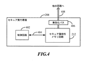
図4に、本開示の一態様による、SEE208の概略ブロック図を示す。SEE208は、セキュア揮発性メモリ回路212と制御回路402となどのSEE208の構成要素の間の通信を可能にするセキュア揮発性メモリ回路212と、制御回路402と、セキュアバスライン404とを含み得る。制御回路402は、ユーザアプリケーション、HLOS、および/またはいくつかの2次ブートローダなどの非セキュアアプリケーションではなく、SEE208によってのみアクセスおよび利用され得る制御論理である。制御回路402は、データがどのようにセキュア揮発性メモリ回路212に記憶され、コピーされ、それから読み取られるかを制御し得る。制御回路402はまた、PUF210(図2参照)の初期論理状態値から導出された秘密データと、場合によっては、追加の補助データとに基づいて秘密鍵を抽出する本明細書で説明する暗号アルゴリズムを実行し得る。制御回路402は、さらに、秘密鍵に基づいて追加の副鍵および/または公開データを生成し得る。したがって、SEE制御回路402は、秘密データに基づいて秘密鍵を抽出するためにSEEにおいて暗号アルゴリズムを実行するための手段の一例を表す。
FIG. 4 shows a schematic block diagram of
セキュア揮発性メモリ回路212は、各々が複数のメモリセルを含む1つまたは複数のセキュア揮発性メモリ回路を含む。セキュア揮発性メモリ回路212は、限定はしないが、eDRAM、SRAMなどの任意のタイプの揮発性メモリであり得る。セキュア揮発性メモリ回路212は、秘密データを記憶し、さらに、秘密データに部分的に基づいて制御論理402によって抽出される秘密鍵を記憶する。SEE208は、セキュア揮発性メモリ回路212の完全な制御を行い、したがって、他のアプリケーション(たとえば、非セキュアアプリケーション)は、セキュア揮発性メモリ回路212にアクセスすることができない。たとえば、SEE208は、IC200の他の非セキュア回路にセキュア揮発性メモリ回路212を結合するあらゆるバス408の線を物理的にロックダウンし得る(無効化バス論理406として示されている)。
Secure
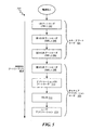
図5に、本開示の一態様による、セキュアブートフロー500の階層を示す。IC200(たとえば、その処理回路203)によって実行され得るセキュアブートフロー500は、セキュアブートローダ501によって部分的に含まれ、非セキュアアプリケーションローダ503によって部分的に含まれ得る。セキュアブートローダ501は、1次ブートローダ(PBL)502と、第1の2次ブートローダ(SBL1)504と、第2の2次ブートローダ(SBL2)506とを含み得る。ブートアッププロセスのこの部分中に無認可のユーザコード(たとえば、HLOS、ユーザアプリケーションなど)は実行および/または注入され得ないので、セキュアブートローダ501によって実行されるコードは「セキュアである」と見なされる。したがって、PUF210(図2参照)の初期論理状態値、そのような初期論理状態値から導出された秘密データ、および/または秘密データに基づいて抽出された秘密鍵に関する情報は、セキュアブートフロー500のこの部分中に損なわれる/無認可のアプリケーションに漏洩されることになるという危険はほとんどない。
FIG. 5 illustrates a hierarchy of a
非セキュアアプリケーションローダ503は、第3の2次ブートローダ(SBL3)508と、アプリケーション2次ブートローダ510と、HLOS512と、ユーザアプリケーション514とを含み得る。非セキュアアプリケーションローダ503は、これらのローダ508、510、512、514のうちの1つまたは複数の実行および/または認証中に無認可のユーザコードが実行および/または注入され得るので、「非セキュアである」と見なされる。
The
図2および図5を参照すると、IC200の電源投入時に、セキュアブートフロー500は、IC200の様々な回路およびモジュールの初期化を含む、IC200の大部分の初期および基本タスクのうちのいくつかを実行する1次ブートローダ502の実行で開始する。PBL502は、ハードワイヤードされ得(たとえば、ROM中に記憶され得)、したがって、事実上改変され得ないので、非常にセキュアである。PBL502はまた、SBL1504が実行する前にSBL1504をロードし、認証する。SBL1504の認証の後に、SBL1504は、実行し、特に、揮発性メモリ回路206の初期論理状態値に基づいて秘密データを導出し、IC200内の他のメモリ回路に秘密データを記憶し得る。SBL1504はまた、RPM回路201を初期化することと、IC200のシステムクロックを構成し、リセットをリリースすることと、SBL2506が実行する前にSBL2506をロードし、認証することとを行い得る。
Referring to FIGS. 2 and 5, upon power-up of IC 200,
SBL2506が認証された後、SBL2506は実行し、特に、非セキュアメモリ回路からセキュア揮発性メモリ回路212に秘密データをコピーし得る。SBL2506はまた、IC200の1つまたは複数の処理回路(たとえば、処理回路203)を初期化することと、IC200の外部のメモリ回路(たとえば、外部DRAMおよび/またはSRAM)を構成することと、SEE208、他のファームウェア、および/またはSBL3508をロードし、認証することとを行い得る。SBL3508の認証の後に、SBL3508は、実行し、特に、ソフトウェアフラッシングのためのストレージモードを検査し得る。SBL3508はまた、HLOS512および/またはアプリケーション2次ブートローダ510をロードし、認証し得る。同様の方法で、後続のブートアッププロセスは、アプリケーション2次ブートローダ510、HLOS512、およびユーザアプリケーション514などの連続する順序でロードされ、認証され、実行される。これらのプロセス502、504、506、508、510、512がロードされて、実行される順序は、図5に示すものと異なり得る。さらに、図5に示した2次ブートローダの数およびタイプならびに他のアプリケーションコードは、例/例示にすぎない。たとえば、本開示の他の態様では、より多いまたはより少ない2次ブートローダがセキュアブートフロー500を含み得る。
After SBL 2 506 is authenticated, SBL 2 506 executes and may copy secret data from non-secure memory circuit to secure
図6に、本開示の一態様による、秘密鍵を抽出し、記憶する、本明細書で説明するセキュアブートフローを採用するIC600を示す。IC600は、RPM回路201、処理回路(たとえば、アプリケーションプロセッサ)203、セキュアブートローダ501、非セキュアアプリケーションブートローダ503、揮発性メモリ回路206、SEE208、および/または不揮発性メモリ回路604を含み得る。セキュアブートローダ501は、PBL502、SBL1504、および/またはSBL2を含み得る。非セキュアアプリケーションブートローダ503は、SBL2506(図5参照)の後に実行するセキュアブートフロー500の一部分のためのブートローダを含み得る。たとえば、非セキュアアプリケーションブートローダ503は、SBL3508、アプリケーション2次ブートローダ510、HLOSコード512、および/またはユーザアプリケーション514を含み得る。揮発性メモリ回路206は、第1の揮発性メモリ回路210(すなわち、PUF)と第2の/予備の揮発性メモリ回路302とを含む。SEE208は、SEE制御回路402と、セキュア揮発性メモリ回路212とを含む。セキュア揮発性メモリ回路212は、PUFの初期論理状態値から導出された秘密データを記憶するように構成された第1のセキュア揮発性メモリ回路608と、秘密鍵を記憶するように構成された第2のセキュア揮発性メモリ回路610とを含む。
FIG. 6 illustrates an IC 600 that employs the secure boot flow described herein to extract and store a secret key according to one aspect of the present disclosure. IC 600 may include
不揮発性メモリ回路604は、補助データ606を含む。一例によれば、不揮発性メモリ回路604は、IC600の一部である(すなわち、「オンチップ」である)。別の例によれば、不揮発性メモリ回路604は、IC600の一部ではなく、IC600と通信している別個の回路である(すなわち、「オフチップ」である)。補助データ606の一部または全部は、非セキュアアプリケーションによってアクセスされ得るので、非セキュアであり得る。第1のセキュア揮発性メモリ回路608は、セキュア揮発性メモリ回路中に秘密データを記憶するための手段の一例を表し、第2のセキュア揮発性メモリ回路610は、セキュア揮発性メモリ回路中に秘密鍵を記憶するための手段の一例を表す。
The nonvolatile memory circuit 604 includes auxiliary data 606. According to one example, non-volatile memory circuit 604 is part of IC 600 (ie, “on-chip”). According to another example, non-volatile memory circuit 604 is not part of IC 600 but is a separate circuit in communication with IC 600 (ie, “off-chip”). Since some or all of the auxiliary data 606 can be accessed by a non-secure application, it can be non-secure. The first secure
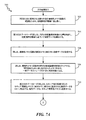
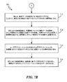
図7Aおよび図7Bを含む図7に、一態様による、集積回路600に秘密鍵を抽出し、記憶することを行わせるセキュアブートフローを示すフローチャート700を示す。図6および図7を参照すると、IC600の電源投入時に、電力は、第1の揮発性メモリ回路210(すなわち、PUFのために使用されるメモリの一部分)を含む揮発性メモリ回路206に供給される。図2に関して上記で説明したように、揮発性メモリ回路206は、SRAMなどの揮発性メモリの一種であり、そのメモリ回路セルは、一般にそれぞれ最初に、各セルに固有の製造詳細により、電源投入時に好適な論理状態に落ち着くことになる。初期論理値は、実質的に繰り返し可能であり、したがって、起動(すなわち、電源投入)時に、セルの大部分が毎回同じ値に落ち着くことになる。したがって、電源投入時に、PUFのために使用される第1の揮発性メモリ回路210を含む揮発性メモリ回路206は、初期論理状態値に落ち着く702。
FIG. 7, including FIGS. 7A and 7B, shows a
次に、第1の2次ブートローダ(SBL1)504は、初期論理状態値が使用されることになる揮発性メモリ回路206のメモリ回路セル(すなわち、第1の揮発性メモリ回路210によって指定されるメモリの一部分)の位置を特定し、それらの初期論理状態値に基づいて秘密データを導出する704。上記で説明したように、秘密データは、初期論理状態値に等しくなり得るか、または秘密データは、初期論理状態値の何らかの関数に基づいて導出され得る。秘密データが導出された後、SBL1504は、揮発性メモリ回路の第2の(すなわち、予備の)メモリ部分302中に秘密データを記憶する706。次いで、SBL1504は、第1の揮発性メモリ回路210の初期論理状態値をクリアし、したがって、初期論理状態値の痕跡が後続のプロセス/アプリケーション(たとえば、非セキュアアプリケーション)によってそれらのメモリアドレスロケーションにおいて発見され得ない。クリアされると、第1の揮発性メモリ回路210は、一般データストレージのために利用可能になる(すなわち、あらゆる後続のプロセス/アプリケーションがその第1の揮発性メモリ回路210を使用し得る)708。
Next, the first secondary boot loader (SBL 1 ) 504 is designated by the memory circuit cell of the volatile memory circuit 206 (i.e., the first volatile memory circuit 210) where the initial logic state value will be used And 704 derive secret data based on their initial logic state values. As explained above, the secret data can be equal to the initial logic state value, or the secret data can be derived based on some function of the initial logic state value. After the secret data is derived, SBL 1 504
次に、第2の2次ブートローダ(SBL2)506は、SEE208のセキュア揮発性メモリ回路212に第2のメモリ部分302中に記憶された秘密データをコピー/転送する。たとえば、秘密データは、第1のセキュア揮発性メモリ回路608に記憶され得る。SBL2506は、次いで、揮発性メモリ回路206中の秘密データのあらゆる痕跡を除去するために、揮発性メモリ回路206の第2のメモリ部分302をクリアする、および/または、揮発性メモリ回路206全体をクリアする。クリアされると、予備のメモリ部分302は、一般データストレージのために利用可能になる(すなわち、あらゆる後続のプロセス/アプリケーションがその予備のメモリ部分302を使用し得る)712。
The second secondary boot loader (SBL 2 ) 506 then copies / transfers the secret data stored in the
さらに、SEE208は、次いで、秘密データに基づいて秘密鍵を抽出する。たとえば、SEE208における制御論理回路402は、第1のセキュア揮発性メモリ回路608に記憶された秘密データと不揮発性メモリ回路604に記憶された補助データ606とを取得する。このデータを取得した後に、制御回路402は、秘密鍵を抽出するための入力として補助データ606と秘密データとを使用して暗号アルゴリズム(たとえば、ブロックコードアルゴリズム、拡散コードアルゴリズム、リピートコードアルゴリズムなどのうちの少なくとも1つ)を実行する。暗号アルゴリズムは、ブートごとに秘密データおよび/または初期論理状態値の間のいくつかの違いにもかかわらず同じ秘密鍵を抽出するために誤り訂正技法を含み得る。秘密鍵はまた、セキュア揮発性メモリ212(たとえば、第2のセキュア揮発性メモリ回路610)中に記憶される714。
Further, the
秘密鍵が、SEE208の制御の範囲内で、セキュア揮発性メモリ回路212にセキュアに記憶されるので、秘密鍵は、他の非セキュアアプリケーションによってアクセスされ得ない。そのような非セキュアアプリケーションは、秘密鍵に基づいて(たとえば、上記で説明したように、暗号化データおよび/または公開データを含む)SEE出力データについての要求をSEE208に送り得る716。SEE208における制御論理回路402は、次いで、秘密鍵に基づいてSEE出力データを生成し、要求元の非セキュアアプリケーションにSEE出力データを与え得る718。
Since the secret key is securely stored in the secure
秘密鍵がセキュア揮発性メモリ212中にのみ記憶されるので、秘密鍵は、IC600が電源切断されると失われる。秘密鍵は、上記で説明したようにPUF210の初期論理状態値に基づいてセキュアブートフロー700を通して電源投入時に再び再抽出されなければならない。秘密鍵が不揮発性メモリ中に記憶されないので、IC600を物理的に開き、メモリ回路を検査することによって秘密鍵への無許可のアクセスを獲得しようと試みる不正な当事者は鍵を取得することができないことになる。
Since the secret key is stored only in the secure
一態様によれば、IC600および/または揮発性メモリ回路206は、リセット時にセキュアブートフロー700が直ちに実行される(たとえば、IC600もリセットされる)ように設計される。一態様によれば、RPM回路201は、揮発性メモリ回路206をリセットすることを単独で管理していることがある。したがって、非セキュアアプリケーションは、PUF210および/または揮発性メモリ回路206をリセットできないし、PUF210の初期論理状態値へのアクセスを獲得することができない。IC600をリセットすることは、動作する非セキュアアプリケーションを終了し、セキュアブートフロー700を再び開始させることになる。
According to one aspect, IC 600 and / or volatile memory circuit 206 are designed such that
一態様によれば、PUF210を構成する特定の揮発性メモリ回路セルは、様々な方法で選択され得る。一例によれば、PUF210メモリセルは、信頼性のために(すなわち、電源投入時に一貫した論理状態値を生成する可能性を増加するために)選定されたメモリ回路セルの連続するブロックであり得る。別の例によれば、PUF210メモリセルは、互いに不連続であり、さらには、揮発性メモリ回路206の様々な部位からランダムに選定され得る。ただし、PUF210を構成する特定の揮発性メモリ回路セルが選定されると、同じ特定の揮発性メモリ回路セルが、PUF210の基礎となるように電源投入時に毎回再び選定される。
According to one aspect, the particular volatile memory circuit cells that make up the
図8に、本開示の一態様による、集積回路において動作可能な方法800を示す。最初に、第1の揮発性メモリ回路が、複数の初期論理状態値を生成するために電源投入され、ここで、第1の揮発性メモリ回路は集積回路上にある802。次に、秘密データが、複数の初期論理状態値に基づいて導出される804。次いで、秘密データが、セキュア揮発性メモリ回路中に記憶され、ここで、セキュア揮発性メモリ回路は、セキュア実行環境(SEE)によってセキュアにされる806。次に、複数の初期論理状態値が、第1の揮発性メモリ回路中でクリアされる808。次いで、暗号アルゴリズムが、秘密データに基づいて秘密鍵を抽出するためにSEEにおいて実行される810。秘密鍵はまた、セキュア揮発性メモリ回路中に記憶される812。一態様によれば、秘密鍵は、複数の初期論理状態値が第1の揮発性メモリ回路中でクリアされる(ステップ808)前に抽出され、記憶され得る(すなわち、ステップ810、812)。
FIG. 8 illustrates a
図9に、本開示の一態様による、IC200、600の処理回路203の概略ブロック図を示す。処理回路203は、秘密データ導出回路902、クリア回路904、および/または暗号アルゴリズム回路906を含み得る。
FIG. 9 shows a schematic block diagram of the processing circuit 203 of the ICs 200, 600 according to one aspect of the present disclosure. The processing circuit 203 may include a secret
図2、図6、図8、および図9を参照すると、秘密データ導出回路902は、複数の初期論理状態値に基づいて秘密データを導出するための手段の一例である。クリア回路904は、第1の揮発性メモリ回路206中の複数の初期論理状態値をクリアするための手段の一例である。暗号アルゴリズム回路906は、秘密データに基づいて秘密鍵を抽出するためにSEE208において暗号アルゴリズムを実行するための手段の一例である。
Referring to FIGS. 2, 6, 8, and 9, secret
図2、図3、図4、図5、図6、図7A、図7B、図8、および図9に示された構成要素、ステップ、特徴、および/または機能のうちの1つまたは複数は、単一の構成要素、ステップ、特徴、もしくは機能へと再構成され、かつ/もしくは組み合わされ、または、いくつかの構成要素、ステップ、もしくは機能で具現化され得る。さらなる要素、構成要素、ステップ、および/または機能も、本発明から逸脱することなく追加され得る。図2、図3、図4、図6、および/または図9に示す装置、デバイス、および/または構成要素は、図5、図7A、図7B、および/または図8で説明する方法、特徴、またはステップのうちの1つまたは複数を実行するように構成され得る。本明細書で説明するアルゴリズムは、ソフトウェアでも効率的に実装され得、および/またはハードウェアにも組み込まれ得る。 One, more than one of the components, steps, features, and / or functions shown in FIG. 2, FIG. 3, FIG. 4, FIG. 5, FIG. 6, FIG. 7A, FIG. 7B, FIG. Can be reconfigured and / or combined into a single component, step, feature, or function, or embodied in several components, steps, or functions. Additional elements, components, steps, and / or functions may also be added without departing from the invention. The apparatus, device, and / or component shown in FIG. 2, FIG. 3, FIG. 4, FIG. 6, and / or FIG. 9 is the method, feature described in FIG. 5, FIG. 7A, FIG. 7B, and / or FIG. Or may be configured to perform one or more of the steps. The algorithms described herein can be efficiently implemented in software and / or incorporated into hardware.
その上、本開示の一態様では、図2、図6、および/または図9に示す処理回路203は、図5、図7A、図7B、および/または図8で説明したアルゴリズム、方法、および/またはステップを実行するように特別に設計かつ/または配線接続される専用プロセッサ(たとえば、特定用途向け集積回路(たとえば、ASIC))であり得る。したがって、そのような専用プロセッサ(たとえば、ASIC)は、図5、図7A、図7B、および/または図8で説明したアルゴリズム、方法、および/またはステップを実行するための手段の一例であり得る。 Moreover, in one aspect of the present disclosure, the processing circuit 203 shown in FIG. 2, FIG. 6, and / or FIG. 9 performs the algorithm, method, and process described in FIG. 5, FIG. 7A, FIG. It can be a dedicated processor (eg, an application specific integrated circuit (eg, ASIC)) that is specifically designed and / or wired to perform the steps. Thus, such a dedicated processor (eg, ASIC) may be an example of a means for performing the algorithms, methods, and / or steps described in FIG. 5, FIG. 7A, FIG. 7B, and / or FIG. .
また、本開示の態様は、フローチャート、流れ図、構造図またはブロック図として示されるプロセスとして説明され得ることに留意されたい。フローチャートは動作を逐次プロセスとして説明し得るが、動作の多くは並行してまたは同時に実行され得る。さらに、動作の順序は並び替えられ得る。プロセスは、その動作が完了したとき、終了する。プロセスは、方法、関数、手順、サブルーチン、サブプログラムなどに対応し得る。プロセスが関数に対応するとき、その終了は、呼出し関数またはmain関数への関数のリターンに対応する。 It should also be noted that aspects of the present disclosure may be described as a process which is depicted as a flowchart, flowchart, structure diagram, or block diagram. Although a flowchart may describe the operations as a sequential process, many of the operations can be performed in parallel or concurrently. Furthermore, the order of operations can be rearranged. The process ends when its operation is complete. A process may correspond to a method, function, procedure, subroutine, subprogram, etc. When a process corresponds to a function, its termination corresponds to a function return to the calling function or main function.
その上、記憶媒体は、読取り専用メモリ(ROM)、ランダムアクセスメモリ(RAM)、磁気ディスク記憶媒体、光学記憶媒体、フラッシュメモリデバイスおよび/もしくは他の機械可読媒体、およびプロセッサ可読媒体、ならびに/または情報を記憶するためのコンピュータ可読媒体を含む、データを記憶するための1つもしくは複数のデバイスを表し得る。「機械可読媒体」、「コンピュータ可読媒体」、および/または「プロセッサ可読媒体」という用語は、限定はしないが、ポータブルもしくは固定ストレージデバイス、光ストレージデバイス、ならびに、命令および/またはデータを記憶または格納することが可能な様々な他の媒体のような非一時的媒体を含み得る。したがって、本明細書で説明される様々な方法は、「機械可読媒体」、「コンピュータ可読媒体」および/または「プロセッサ可読媒体」に記憶され、1つもしくは複数のプロセッサ、機械および/またはデバイスによって実行され得る命令および/またはデータによって、完全にまたは部分的に実装され得る。 Moreover, the storage media can be read only memory (ROM), random access memory (RAM), magnetic disk storage media, optical storage media, flash memory devices and / or other machine readable media, and processor readable media, and / or It may represent one or more devices for storing data, including computer readable media for storing information. The terms “machine-readable medium”, “computer-readable medium”, and / or “processor-readable medium” include, but are not limited to, portable or fixed storage devices, optical storage devices, and instructions and / or data. It may include non-transitory media such as various other media that can be used. Accordingly, the various methods described herein may be stored on a “machine-readable medium”, “computer-readable medium”, and / or “processor-readable medium” by one or more processors, machines, and / or devices. Depending on the instructions and / or data that can be executed, it can be implemented completely or partially.
さらに、本開示の態様は、ハードウェア、ソフトウェア、ファームウェア、ミドルウェア、マイクロコード、またはそれらの任意の組合せによって実装され得る。ソフトウェア、ファームウェア、ミドルウェアまたはマイクロコードで実装されるとき、必要なタスクを実行するプログラムコードまたはコードセグメントは、記憶媒体または他のストレージのような機械可読媒体に記憶され得る。プロセッサは、必要なタスクを実行し得る。コードセグメントは、手順、関数、サブプログラム、プログラム、ルーチン、サブルーチン、モジュール、ソフトウェアパッケージ、クラス、または命令、データ構造もしくはプログラムステートメントの任意の組合せを表し得る。コードセグメントは、情報、データ、引数、パラメータ、またはメモリ内容を渡すことおよび/または受け取ることによって、別のコードセグメントまたはハードウェア回路に結合され得る。情報、引数、パラメータ、データなどは、メモリ共有、メッセージパッシング、トークンパッシング、ネットワーク送信などを含む、任意の適切な手段を介して渡されてもよく、転送されてもよく、または送信され得る。 Furthermore, aspects of the present disclosure may be implemented by hardware, software, firmware, middleware, microcode, or any combination thereof. When implemented in software, firmware, middleware, or microcode, program code or code segments that perform the required tasks may be stored on a machine-readable medium, such as a storage medium or other storage. The processor may perform the necessary tasks. A code segment can represent a procedure, function, subprogram, program, routine, subroutine, module, software package, class, or any combination of instructions, data structures, or program statements. A code segment may be coupled to another code segment or a hardware circuit by passing and / or receiving information, data, arguments, parameters, or memory contents. Information, arguments, parameters, data, etc. may be passed, forwarded, or transmitted via any suitable means including memory sharing, message passing, token passing, network transmission, etc.
本明細書で開示する例に関して説明する様々な例示的な論理ブロック、モジュール、回路、要素、および/または構成要素は、汎用プロセッサ、デジタル信号プロセッサ(DSP)、特定用途向け集積回路(ASIC)、フィールドプログラマブルゲートアレイ(FPGA)もしくは他のプログラマブル論理構成要素、個別ゲートもしくはトランジスタ論理、個別ハードウェア構成要素、または本明細書で説明する機能を実施するように設計されたそれらの任意の組合せで実装または実施され得る。汎用プロセッサはマイクロプロセッサであり得るが、代替形態では、プロセッサは、任意の従来のプロセッサ、コントローラ、マイクロコントローラ、または状態機械であり得る。プロセッサはまた、コンピューティング構成要素の組合せ、たとえば、DSPとマイクロプロセッサとの組合せ、いくつかのマイクロプロセッサ、DSPコアと連係した1つもしくは複数のマイクロプロセッサ、または他の任意のそのような構成として実装され得る。 Various exemplary logic blocks, modules, circuits, elements, and / or components described with respect to the examples disclosed herein include general purpose processors, digital signal processors (DSPs), application specific integrated circuits (ASICs), Implemented in a field programmable gate array (FPGA) or other programmable logic components, individual gate or transistor logic, individual hardware components, or any combination thereof designed to perform the functions described herein Or it can be implemented. A general purpose processor may be a microprocessor, but in the alternative, the processor may be any conventional processor, controller, microcontroller, or state machine. A processor can also be a combination of computing components, such as a combination of a DSP and a microprocessor, several microprocessors, one or more microprocessors associated with a DSP core, or any other such configuration. Can be implemented.
本明細書で開示する例に関して説明する方法またはアルゴリズムは、直接ハードウェアにおいて、プロセッサによって実行可能なソフトウェアモジュールにおいて、または両方の組合せにおいて、処理ユニット、プログラミング命令、または他の指示の形態で実施されてもよく、かつ、単一のデバイスに含まれてもよく、または複数のデバイスにわたって分散され得る。ソフトウェアモジュールは、RAMメモリ、フラッシュメモリ、ROMメモリ、EPROMメモリ、EEPROMメモリ、レジスタ、ハードディスク、リムーバブルディスク、CD-ROM、または当技術分野において知られている任意の他の形態の記憶媒体に常駐し得る。プロセッサが記憶媒体から情報を読み取り、記憶媒体に情報を書き込むことができるように、記憶媒体はプロセッサに結合され得る。代替として、記憶媒体はプロセッサに一体化され得る。 The methods or algorithms described with respect to the examples disclosed herein may be implemented in the form of processing units, programming instructions, or other instructions, directly in hardware, in software modules executable by a processor, or in a combination of both. And may be included in a single device or distributed across multiple devices. A software module resides in RAM memory, flash memory, ROM memory, EPROM memory, EEPROM memory, registers, hard disk, removable disk, CD-ROM, or any other form of storage medium known in the art. obtain. The storage medium may be coupled to the processor such that the processor can read information from, and write information to, the storage medium. In the alternative, the storage medium may be integral to the processor.
さらに、本明細書で開示する態様に関して説明する様々な例示的な論理ブロック、モジュール、回路、およびアルゴリズムステップは、電子ハードウェア、コンピュータソフトウェア、または両方の組合せとして実装され得ることを当業者は諒解されよう。ハードウェアとソフトウェアのこの互換性を明確に示すために、様々な例示的な構成要素、ブロック、モジュール、回路、およびステップが、上記では概してそれらの機能に関して説明した。そのような機能性が、ハードウェアまたはソフトウェアのどちらとして実施されるのかは、具体的な適用例と、システム全体に課せられる設計制約とによって決まる。 Moreover, those skilled in the art will appreciate that the various exemplary logic blocks, modules, circuits, and algorithm steps described with respect to aspects disclosed herein can be implemented as electronic hardware, computer software, or a combination of both. Let's do it. To clearly illustrate this interchangeability of hardware and software, various illustrative components, blocks, modules, circuits, and steps have been described above generally in terms of their functionality. Whether such functionality is implemented as hardware or software depends upon the specific application and design constraints imposed on the overall system.
本明細書で説明する本発明の様々な特徴は、本発明から逸脱することなく、異なるシステムにおいて実施され得る。本開示の前述の態様は、単に例であり、本発明を限定するものとして解釈されるべきではないことに留意されたい。本開示の態様の説明は、例示であることを意図しており、特許請求の範囲を限定することを意図していない。したがって、本教示は、他のタイプの装置に容易に適用されることが可能であり、多くの代替形態、変更形態、および変形形態が当業者には明らかであろう。 Various features of the invention described herein can be implemented in different systems without departing from the invention. It should be noted that the foregoing aspects of the disclosure are merely examples and should not be construed as limiting the invention. The descriptions of aspects of the disclosure are intended to be illustrative and are not intended to limit the scope of the claims. Thus, the present teachings can be readily applied to other types of devices, and many alternatives, modifications, and variations will be apparent to those skilled in the art.
100 集積回路(IC)、IC、集積回路
102 ブートローダ
104 ユーザアプリケーション
106 メモリ回路、不揮発性メモリ回路
108 暗号鍵、鍵
200 集積回路(IC)、IC
201 リソース電力管理(RPM)回路、RPM回路
202 セキュアブートローダ、セキュアブートローダ回路
203 処理回路
204 非セキュアアプリケーション
206 メモリ回路、揮発性メモリモジュール/回路、揮発性メモリ回路
208 セキュア実行環境(SEE)、SEE
210 PUFメモリ回路、PUF、メモリモジュール/回路、メモリ回路、第1の揮発性メモリ回路、物理的クローン不能関数(PUF)
212 セキュア揮発性メモリ、セキュア揮発性メモリ回路、メモリ回路
302 メモリモジュール/回路、メモリ回路、揮発性メモリモジュール/回路、第2の/予備の揮発性メモリ回路、第2の揮発性メモリ回路、第2のメモリ部分、予備のメモリ部分
304 メモリモジュール/回路、メモリ回路、揮発性メモリモジュール/回路
306 メモリモジュール/回路、メモリ回路、揮発性メモリモジュール/回路
402 SEE制御回路、制御回路、制御論理、制御論理回路
404 セキュアバスライン
406 無効化バス論理
408 バス
500 セキュアブートフロー
501 セキュアブートローダ
502 1次ブートローダ(PBL)、PBL、プロセス
503 非セキュアアプリケーションブートローダ、非セキュアアプリケーションローダ
504 第1の2次ブートローダ(SBL1)、SBL1、プロセス
506 第2の2次ブートローダ(SBL2)、SBL2、プロセス
508 第3の2次ブートローダ(SBL3)、SBL3、プロセス、ローダ
510 アプリケーション2次ブートローダ、プロセス、ローダ
512 HLOS、HLOSコード、プロセス、ローダ
514 ユーザアプリケーション、ローダ
600 集積回路、IC
604 不揮発性メモリ回路
606 補助データ
608 第1のセキュア揮発性メモリ回路
610 第2のセキュア揮発性メモリ回路
902 秘密データ導出回路
904 クリア回路
906 暗号アルゴリズム回路
100 Integrated circuits (ICs), ICs, integrated circuits
102 Boot loader
104 User application
106 Memory circuit, non-volatile memory circuit
108 Encryption key, key
200 Integrated circuit (IC), IC
201 Resource power management (RPM) circuit, RPM circuit
202 Secure Boot Loader, Secure Boot Loader Circuit
203 Processing circuit
204 Non-secure application
206 Memory circuits, volatile memory modules / circuits, volatile memory circuits
208 Secure Execution Environment (SEE), SEE
210 PUF memory circuit, PUF, memory module / circuit, memory circuit, first volatile memory circuit, physical non-cloneable function (PUF)
212 Secure volatile memory, secure volatile memory circuit, memory circuit
302 memory module / circuit, memory circuit, volatile memory module / circuit, second / spare volatile memory circuit, second volatile memory circuit, second memory part, spare memory part
304 Memory module / circuit, memory circuit, volatile memory module / circuit
306 Memory module / circuit, memory circuit, volatile memory module / circuit
402 SEE control circuit, control circuit, control logic, control logic circuit
404 secure bus line
406 Invalidation bus logic
408 bus
500 secure boot flow
501 secure boot loader
502 Primary boot loader (PBL), PBL, process
503 Non-secure application boot loader, non-secure application loader
504 First secondary bootloader (SBL 1 ), SBL 1 , process
506 Second secondary bootloader (SBL 2 ), SBL 2 , process
508 Third secondary boot loader (SBL 3 ), SBL 3 , process, loader
510 Application secondary bootloader, process, loader
512 HLOS, HLOS code, process, loader
514 User application, loader
600 Integrated circuits, IC
604 Nonvolatile memory circuit
606 auxiliary data
608 First secure volatile memory circuit
610 Second Secure Volatile Memory Circuit
902 Secret data derivation circuit
904 Clear circuit
906 Cryptographic algorithm circuit
Claims (30)
複数の初期論理状態値を生成するために第1の揮発性メモリ回路を電源投入するステップであって、前記第1の揮発性メモリ回路が前記集積回路上にある、ステップと、
前記複数の初期論理状態値に基づいて秘密データを導出するステップと、
セキュア揮発性メモリ回路中に前記秘密データを記憶するステップであって、前記セキュア揮発性メモリ回路が、セキュア実行環境(SEE)によってセキュアにされる、ステップと、
前記第1の揮発性メモリ回路中の前記複数の初期論理状態値をクリアするステップと、
前記秘密データに基づいて秘密鍵を抽出するために前記SEEにおいて暗号アルゴリズムを実行するステップと、
前記セキュア揮発性メモリ回路中に前記秘密鍵を記憶するステップと
を含む方法。 A method operable in an integrated circuit comprising:
Powering up a first volatile memory circuit to generate a plurality of initial logic state values, wherein the first volatile memory circuit is on the integrated circuit; and
Deriving secret data based on the plurality of initial logic state values;
Storing the secret data in a secure volatile memory circuit, wherein the secure volatile memory circuit is secured by a secure execution environment (SEE);
Clearing the plurality of initial logic state values in the first volatile memory circuit;
Executing a cryptographic algorithm in the SEE to extract a secret key based on the secret data;
Storing the secret key in the secure volatile memory circuit.
前記秘密鍵が、前記セキュアブートフロー中に、および前記1つまたは複数の非セキュアアプリケーションの実行より前に、抽出され、前記セキュア揮発性メモリ回路中に記憶される、請求項3に記載の方法。 The secure boot flow includes a primary boot loader, a first secondary boot loader, and a second secondary boot loader, and the secure boot flow includes the primary boot loader prior to execution by the first secondary boot loader. Establishing a trust chain by having the boot loader authenticate the first secondary boot loader, and the first secondary boot loader authenticates the second secondary boot loader before the second secondary boot loader executes And the second secondary boot loader authenticates the SEE,
The method of claim 3, wherein the private key is extracted and stored in the secure volatile memory circuit during the secure boot flow and prior to execution of the one or more non-secure applications. .
前記セキュア揮発性メモリ回路中に前記秘密データを記憶した後に前記第2の揮発性メモリ回路中に記憶された前記秘密データをクリアするステップと
をさらに含む、請求項1に記載の方法。 Storing the secret data in a second volatile memory circuit prior to storing the secret data in the secure volatile memory circuit;
The method of claim 1, further comprising: clearing the secret data stored in the second volatile memory circuit after storing the secret data in the secure volatile memory circuit.
副鍵および/または公開データのうちの少なくとも1つについて前記SEEにおいて前記非セキュアアプリケーションから要求を受信するステップと、
前記秘密鍵に基づいて前記SEEにおいて前記副鍵および/または前記公開データを生成するステップと、
前記副鍵および/または前記公開データを要求する前記非セキュアアプリケーションに前記副鍵および/または前記公開データを与えるステップと
をさらに含む、請求項1に記載の方法。 The SEE controls access to the secret key by making the secret key inaccessible from non-secure applications, the method comprising:
Receiving a request from the non-secure application at the SEE for at least one of a subkey and / or public data;
Generating the subkey and / or the public data in the SEE based on the secret key;
2. The method of claim 1, further comprising: providing the subkey and / or the public data to the non-secure application that requests the subkey and / or the public data.
電源投入時に複数の初期論理状態値を生成するように構成された第1の揮発性メモリ回路と、
セキュア実行環境(SEE)によってセキュアにされるセキュア揮発性メモリ回路と、
前記第1の揮発性メモリ回路と前記セキュア揮発性メモリ回路とに通信可能に結合された処理回路であって、
前記複数の初期論理状態値に基づいて秘密データを導出することと、
前記セキュア揮発性メモリ回路中に前記秘密データを記憶することと、
前記第1の揮発性メモリ回路中の前記複数の初期論理状態値をクリアすることと、
前記秘密データに基づいて秘密鍵を抽出するために前記SEEにおいて暗号アルゴリズムを実行することと、
前記セキュア揮発性メモリ回路中に前記秘密鍵を記憶することと
を行うように構成された処理回路と
を含む集積回路。 An integrated circuit,
A first volatile memory circuit configured to generate a plurality of initial logic state values upon power-up;
A secure volatile memory circuit secured by a secure execution environment (SEE);
A processing circuit communicatively coupled to the first volatile memory circuit and the secure volatile memory circuit;
Deriving secret data based on the plurality of initial logic state values;
Storing the secret data in the secure volatile memory circuit;
Clearing the plurality of initial logic state values in the first volatile memory circuit;
Executing a cryptographic algorithm in the SEE to extract a secret key based on the secret data;
And a processing circuit configured to store the secret key in the secure volatile memory circuit.
前記秘密鍵が、前記セキュアブートフロー中に、および前記1つまたは複数の非セキュアアプリケーションの実行より前に、抽出され、前記セキュア揮発性メモリ回路中に記憶される、請求項19に記載の集積回路。 The secure boot flow includes a primary boot loader, a first secondary boot loader, and a second secondary boot loader, and the secure boot flow includes the primary boot loader prior to execution by the first secondary boot loader. Establishing a trust chain by having the boot loader authenticate the first secondary boot loader, and the first secondary boot loader authenticates the second secondary boot loader before the second secondary boot loader executes And the second secondary boot loader authenticates the SEE,
The integration of claim 19, wherein the secret key is extracted and stored in the secure volatile memory circuit during the secure boot flow and prior to execution of the one or more non-secure applications. circuit.
前記セキュア揮発性メモリ回路中に前記秘密データを記憶するより前に第2の揮発性メモリ回路中に前記秘密データを記憶することと、
前記セキュア揮発性メモリ回路中に前記秘密データを記憶した後に前記第2の揮発性メモリ回路中に記憶された前記秘密データをクリアすることと
を行うようにさらに構成された、請求項17に記載の集積回路。 The processing circuit is
Storing the secret data in a second volatile memory circuit prior to storing the secret data in the secure volatile memory circuit;
18. The method of claim 17, further comprising: clearing the secret data stored in the second volatile memory circuit after storing the secret data in the secure volatile memory circuit. Integrated circuit.
副鍵および/または公開データのうちの少なくとも1つについて前記SEEにおいて前記非セキュアアプリケーションから要求を受信することと、
前記秘密鍵に基づいて前記SEEにおいて前記副鍵および/または前記公開データを生成することと、
前記副鍵および/または前記公開データを要求する前記非セキュアアプリケーションに前記副鍵および/または前記公開データを与えることと
を行うようにさらに構成された、請求項17に記載の集積回路。 The SEE controls access to the secret key by making the secret key inaccessible from non-secure applications, and the processing circuit includes:
Receiving a request from the non-secure application at the SEE for at least one of a subkey and / or public data;
Generating the subkey and / or the public data in the SEE based on the secret key;
18. The integrated circuit of claim 17, further configured to: provide the subkey and / or the public data to the non-secure application that requests the subkey and / or the public data.
複数の初期論理状態値を生成するために第1の揮発性メモリ回路を電源投入するための手段であって、前記第1の揮発性メモリ回路が前記集積回路上にある、手段と、
前記複数の初期論理状態値に基づいて秘密データを導出するための手段と、
セキュア揮発性メモリ回路中に前記秘密データを記憶するための手段であって、前記セキュア揮発性メモリ回路が、セキュア実行環境(SEE)によってセキュアにされる、手段と、
前記第1の揮発性メモリ回路中の前記複数の初期論理状態値をクリアするための手段と、
前記秘密データに基づいて秘密鍵を抽出するために前記SEEにおいて暗号アルゴリズムを実行するための手段と、
前記セキュア揮発性メモリ回路中に前記秘密鍵を記憶するための手段と
を含む集積回路。 An integrated circuit,
Means for powering on a first volatile memory circuit to generate a plurality of initial logic state values, wherein the first volatile memory circuit is on the integrated circuit;
Means for deriving secret data based on the plurality of initial logic state values;
Means for storing the secret data in a secure volatile memory circuit, wherein the secure volatile memory circuit is secured by a secure execution environment (SEE);
Means for clearing the plurality of initial logic state values in the first volatile memory circuit;
Means for executing a cryptographic algorithm in the SEE to extract a secret key based on the secret data;
Means for storing the secret key in the secure volatile memory circuit.
複数の初期論理状態値を生成するために第1の揮発性メモリ回路を電源投入することであって、前記第1の揮発性メモリ回路が前記集積回路上にある、電源投入することと、
前記複数の初期論理状態値に基づいて秘密データを導出することと、
セキュア揮発性メモリ回路中に前記秘密データを記憶することであって、前記セキュア揮発性メモリ回路が、セキュア実行環境(SEE)によってセキュアにされる、記憶することと、
前記第1の揮発性メモリ回路中の前記複数の初期論理状態値をクリアすることと、
前記秘密データに基づいて秘密鍵を抽出するために前記SEEにおいて暗号アルゴリズムを実行することと、
前記セキュア揮発性メモリ回路中に前記秘密鍵を記憶することと
を行わせるコンピュータ可読記憶媒体。 A computer readable storage medium storing one or more instructions, wherein the instructions are executed on the integrated circuit when executed by at least one integrated circuit.
Powering up a first volatile memory circuit to generate a plurality of initial logic state values, wherein the first volatile memory circuit is on the integrated circuit; and
Deriving secret data based on the plurality of initial logic state values;
Storing the secret data in a secure volatile memory circuit, wherein the secure volatile memory circuit is secured by a secure execution environment (SEE);
Clearing the plurality of initial logic state values in the first volatile memory circuit;
Executing a cryptographic algorithm in the SEE to extract a secret key based on the secret data;
A computer readable storage medium for causing the secret key to be stored in the secure volatile memory circuit.
Applications Claiming Priority (3)
| Application Number | Priority Date | Filing Date | Title |
|---|---|---|---|
| US14/161,185 | 2014-01-22 | ||
| US14/161,185 US9755831B2 (en) | 2014-01-22 | 2014-01-22 | Key extraction during secure boot |
| PCT/US2015/011991 WO2015112479A1 (en) | 2014-01-22 | 2015-01-20 | Key extraction during secure boot |
Publications (2)
| Publication Number | Publication Date |
|---|---|
| JP2017504267A true JP2017504267A (en) | 2017-02-02 |
| JP2017504267A5 JP2017504267A5 (en) | 2018-02-15 |
Family
ID=52469304
Family Applications (1)
| Application Number | Title | Priority Date | Filing Date |
|---|---|---|---|
| JP2016546025A Pending JP2017504267A (en) | 2014-01-22 | 2015-01-20 | Key extraction during secure boot |
Country Status (7)
| Country | Link |
|---|---|
| US (1) | US9755831B2 (en) |
| EP (1) | EP3097507A1 (en) |
| JP (1) | JP2017504267A (en) |
| KR (1) | KR20160111455A (en) |
| CN (1) | CN106415585A (en) |
| BR (1) | BR112016016861A2 (en) |
| WO (1) | WO2015112479A1 (en) |
Families Citing this family (14)
| Publication number | Priority date | Publication date | Assignee | Title |
|---|---|---|---|---|
| EP3040896A1 (en) * | 2014-12-30 | 2016-07-06 | Gemalto Sa | Secure element |
| US10496811B2 (en) * | 2016-08-04 | 2019-12-03 | Data I/O Corporation | Counterfeit prevention |
| US11012246B2 (en) * | 2016-09-08 | 2021-05-18 | Taiwan Semiconductor Manufacturing Co., Ltd. | SRAM-based authentication circuit |
| WO2018054537A1 (en) * | 2016-09-24 | 2018-03-29 | Giesecke+Devrient Mobile Security Gmbh | Method and system for downloading operating systems on smart cards having low random access memory |
| US10984136B2 (en) * | 2017-04-21 | 2021-04-20 | Micron Technology, Inc. | Secure memory device with unique identifier for authentication |
| US10812269B2 (en) * | 2017-11-07 | 2020-10-20 | Arris Enterprises Llc | Advanced crypto token authentication |
| US10742406B2 (en) * | 2018-05-03 | 2020-08-11 | Micron Technology, Inc. | Key generation and secure storage in a noisy environment |
| US11010309B2 (en) * | 2018-05-18 | 2021-05-18 | Intel Corporation | Computer system and method for executing one or more software applications, host computer device and method for a host computer device, memory device and method for a memory device and non-transitory computer readable medium |
| US11244078B2 (en) | 2018-12-07 | 2022-02-08 | Nxp Usa, Inc. | Side channel attack protection |
| TWI804703B (en) * | 2019-12-31 | 2023-06-11 | 新唐科技股份有限公司 | Computer apparatus and authority management method based on trust chain |
| US11768611B2 (en) | 2020-04-02 | 2023-09-26 | Axiado Corporation | Secure boot of a processing chip |
| US20220229937A1 (en) * | 2021-01-19 | 2022-07-21 | Cirrus Logic International Semiconductor Ltd. | Integrated circuit with asymmetric access privileges |
| US11809334B2 (en) * | 2021-01-19 | 2023-11-07 | Cirrus Logic Inc. | Integrated circuit with asymmetric access privileges |
| US20230317158A1 (en) * | 2022-03-30 | 2023-10-05 | Crossbar, Inc. | Error correction for identifier data generated from unclonable characteristics of resistive memory |
Citations (3)
| Publication number | Priority date | Publication date | Assignee | Title |
|---|---|---|---|---|
| US20120210115A1 (en) * | 2011-02-11 | 2012-08-16 | Park Dong-Jin | Secure Boot Method and Method for Generating a Secure Boot Image |
| JP2013126221A (en) * | 2011-12-16 | 2013-06-24 | Toshiba Corp | Encryption key generation device and program |
| JP2013545340A (en) * | 2010-10-04 | 2013-12-19 | イントリンシツク・イー・デー・ベー・ベー | Physically non-replicatable function with improved starting behavior |
Family Cites Families (4)
| Publication number | Priority date | Publication date | Assignee | Title |
|---|---|---|---|---|
| US5363447A (en) * | 1993-03-26 | 1994-11-08 | Motorola, Inc. | Method for loading encryption keys into secure transmission devices |
| US6675303B1 (en) * | 1999-09-29 | 2004-01-06 | 2Micro International Limited | PC card controller with advanced power management reset capabilities |
| US20130051552A1 (en) | 2010-01-20 | 2013-02-28 | Héléna Handschuh | Device and method for obtaining a cryptographic key |
| KR101622447B1 (en) | 2010-11-05 | 2016-05-31 | 인터디지탈 패튼 홀딩스, 인크 | Device validation, distress indication, and remediation |
-
2014
- 2014-01-22 US US14/161,185 patent/US9755831B2/en active Active
-
2015
- 2015-01-20 BR BR112016016861A patent/BR112016016861A2/en not_active IP Right Cessation
- 2015-01-20 KR KR1020167022517A patent/KR20160111455A/en not_active Application Discontinuation
- 2015-01-20 CN CN201580004899.7A patent/CN106415585A/en active Pending
- 2015-01-20 WO PCT/US2015/011991 patent/WO2015112479A1/en active Application Filing
- 2015-01-20 EP EP15704127.8A patent/EP3097507A1/en not_active Withdrawn
- 2015-01-20 JP JP2016546025A patent/JP2017504267A/en active Pending
Patent Citations (3)
| Publication number | Priority date | Publication date | Assignee | Title |
|---|---|---|---|---|
| JP2013545340A (en) * | 2010-10-04 | 2013-12-19 | イントリンシツク・イー・デー・ベー・ベー | Physically non-replicatable function with improved starting behavior |
| US20120210115A1 (en) * | 2011-02-11 | 2012-08-16 | Park Dong-Jin | Secure Boot Method and Method for Generating a Secure Boot Image |
| JP2013126221A (en) * | 2011-12-16 | 2013-06-24 | Toshiba Corp | Encryption key generation device and program |
Also Published As
| Publication number | Publication date |
|---|---|
| EP3097507A1 (en) | 2016-11-30 |
| US20150207624A1 (en) | 2015-07-23 |
| CN106415585A (en) | 2017-02-15 |
| KR20160111455A (en) | 2016-09-26 |
| BR112016016861A2 (en) | 2017-08-08 |
| US9755831B2 (en) | 2017-09-05 |
| WO2015112479A1 (en) | 2015-07-30 |
Similar Documents
| Publication | Publication Date | Title |
|---|---|---|
| US9755831B2 (en) | Key extraction during secure boot | |
| US9842212B2 (en) | System and method for a renewable secure boot | |
| US8719585B2 (en) | Secure update of boot image without knowledge of secure key | |
| US20200153808A1 (en) | Method and System for an Efficient Shared-Derived Secret Provisioning Mechanism | |
| US20210240869A1 (en) | Secure memory device with unique identifier for authentication | |
| US9830456B2 (en) | Trust transference from a trusted processor to an untrusted processor | |
| CN104252881B (en) | Semiconductor integrated circuit and system | |
| EP3284000B1 (en) | Secure software authentication and verification | |
| Eisenbarth et al. | Reconfigurable trusted computing in hardware | |
| US8478973B2 (en) | System and method for providing a secure application fragmentation environment | |
| US20150242614A1 (en) | Provisioning of security credentials | |
| US20130254906A1 (en) | Hardware and Software Association and Authentication | |
| US20090204803A1 (en) | Handling of secure storage key in always on domain | |
| US20140270177A1 (en) | Hardening inter-device secure communication using physically unclonable functions | |
| US10057224B2 (en) | System and method for initializing a shared secret system | |
| US10735190B1 (en) | Persistent TPM-based identifier and key pair | |
| US10936722B2 (en) | Binding of TPM and root device | |
| US20140344581A1 (en) | Secure Upgrades for Field Programmable Devices | |
| WO2017112104A1 (en) | Derived keys for execution environments in a boot chain | |
| US20090204801A1 (en) | Mechanism for secure download of code to a locked system | |
| US11874928B2 (en) | Security device, electronic device, secure boot management system, method for generating boot image, and method for executing boot chain | |
| US10461926B2 (en) | Cryptographic evidence of persisted capabilities | |
| Mohammad et al. | Required policies and properties of the security engine of an SoC | |
| US20200235917A1 (en) | Shared secret generation | |
| CN111357003A (en) | Data protection in a pre-operating system environment |
Legal Events
| Date | Code | Title | Description |
|---|---|---|---|
| A521 | Request for written amendment filed |
Free format text: JAPANESE INTERMEDIATE CODE: A523 Effective date: 20160725 |
|
| A521 | Request for written amendment filed |
Free format text: JAPANESE INTERMEDIATE CODE: A523 Effective date: 20171226 |
|
| A621 | Written request for application examination |
Free format text: JAPANESE INTERMEDIATE CODE: A621 Effective date: 20171226 |
|
| A977 | Report on retrieval |
Free format text: JAPANESE INTERMEDIATE CODE: A971007 Effective date: 20180928 |
|
| A131 | Notification of reasons for refusal |
Free format text: JAPANESE INTERMEDIATE CODE: A131 Effective date: 20181015 |
|
| A02 | Decision of refusal |
Free format text: JAPANESE INTERMEDIATE CODE: A02 Effective date: 20190527 |