JP2017201431A - Display device and terminal device - Google Patents
Display device and terminal device Download PDFInfo
- Publication number
- JP2017201431A JP2017201431A JP2017152120A JP2017152120A JP2017201431A JP 2017201431 A JP2017201431 A JP 2017201431A JP 2017152120 A JP2017152120 A JP 2017152120A JP 2017152120 A JP2017152120 A JP 2017152120A JP 2017201431 A JP2017201431 A JP 2017201431A
- Authority
- JP
- Japan
- Prior art keywords
- pixel
- line
- adjacent
- gate line
- data
- Prior art date
- Legal status (The legal status is an assumption and is not a legal conclusion. Google has not performed a legal analysis and makes no representation as to the accuracy of the status listed.)
- Granted
Links
Images


Abstract
Description
本発明は、複数の視点に向けて夫々画像を表示することができる表示パネル等に関し、高画質表示が可能な表示パネル等に関する。 The present invention relates to a display panel or the like that can display images toward a plurality of viewpoints, and more particularly to a display panel or the like capable of high-quality display.
近時の技術進展により、表示パネルはモニタ及びテレビ受像機等の大型の端末装置のみならず、ノート型パーソナルコンピュータ、キャッシュディスペンサ及び自動販売機等の中型の端末装置、パーソナルTV、PDA(Personal Digital Assistance:個人用情報端末)、携帯電話、携帯ゲーム機等の小型の端末装置にまで搭載され、様々な場所で使用されている。特に、液晶を使用した液晶表示装置は、薄型、軽量、小型、低消費電力等の多くの利点を有するため、様々な端末装置に搭載されている。現在の表示装置は正面方向以外の場所から観察した場合でも、正面方向と同じ内容が視認されるが、観察者がディスプレイを視認する位置、すなわち視点により異なる画像が視認可能な表示装置も開発されており、次世代の表示装置として期待されている。 Due to recent technological progress, the display panel is not only a large terminal device such as a monitor and a television receiver, but also a medium-sized terminal device such as a notebook personal computer, a cash dispenser and a vending machine, a personal TV, a PDA (Personal Digital). (Assistance: personal information terminal), small-sized terminal devices such as mobile phones and portable game machines, and are used in various places. In particular, liquid crystal display devices using liquid crystals have many advantages such as thinness, light weight, small size, and low power consumption, and thus are mounted on various terminal devices. Even when the current display device is observed from a location other than the front direction, the same content as the front direction is visually recognized, but a display device in which different images can be visually recognized depending on the position at which the observer visually recognizes the display, that is, the viewpoint has been developed. It is expected as a next-generation display device.
複数の視点に向けて夫々異なる画像を表示可能な装置の一例として、立体画像表示装置を挙げることができる。特に、特殊な眼鏡を装着する必要のない立体画像表示方式として、レンチキュラレンズ方式やパララックスバリア方式が提案されている。 As an example of an apparatus that can display different images for a plurality of viewpoints, a stereoscopic image display apparatus can be given. In particular, a lenticular lens method and a parallax barrier method have been proposed as a stereoscopic image display method that does not require wearing special glasses.
これまでに本発明者は、レンチキュラレンズ等の画像分離用の光学手段を設けた複数視点用表示装置について鋭意検討を重ね、高画質化を実現する方法を開発してきた(例えば、特許文献1参照)。図34は、特許文献1に記載の従来の画像表示装置における表示パネルを示す平面図である。図34に示すように、表示パネルの開口部1075は、平面視で台形を含む形状になっている。具体的には、開口部1075は、左右対称の台形と、この台形の下底の長さと長辺の長さが等しい長方形とを、台形の下底と長方形の長辺とが相互に接触するように配置することにより形成される六角形状である。
So far, the present inventor has intensively studied a multi-viewpoint display device provided with optical means for image separation such as a lenticular lens, and has developed a method for realizing high image quality (see, for example, Patent Document 1). ). FIG. 34 is a plan view showing a display panel in the conventional image display device described in
レンチキュラレンズを構成するシリンドリカルレンズ1003aの長手方向を縦方向1011、配列方向を横方向1012とすると、開口部75の形状は縦方向1011に延びる線分に対して左右対称である。更に、縦方向1011に対して相互に反対の方向に傾斜すると共に、その延びる方向と縦方向1011とがなす角度の大きさが同一である1対の辺が配置されている。この結果、横方向1012においては、表示パネルの開口部1075の端部の位置と、シリンドリカルレンズ1003aの光軸の位置とが、縦方向1011において相対的に異なっている。
更に、縦方向1011に相互に隣接する開口部1075は、横方向1012に延びる線分に対して線対称になるように配置されている。また、横方向1012に相互に隣接する開口部1075は、その縦方向1011における両端部の中点を結んだ線分と、横方向1012における両端部の中点を結んだ線分との交点に対して、点対称になるように配置されている。このため、横方向1012に相互に隣接する開口部1075の分も合算すると、縦方向1011における開口部1075の幅は、横方向1012の位置に拘わらず、略一定となっている。
When the longitudinal direction of the
Further, the
なお、遮光部1076は、画素の縦方向1011に対して傾斜している縁には設けられておらず、画素の横方向1011に延びる縁にのみ設けられている。そして、横方向1012において相互に隣接する開口部1075は、配線1070により区画され、この配線70により遮光されている。
Note that the light-
この特許文献1に記載の表示装置においては、各画素の開口部を台形を含む形状にし、かつ隣接画素の開口部を点対称又は線対称の関係に配置することにより、横方向1012の任意位置において、縦方向1011の開口率を略一定にすることができる。この結果、遮光領域に起因する表示品質の低下を完全に防止することができる。
In the display device described in
また、複数の視点に向けて夫々異なる画像を表示可能な装置の他の例として、複数の異なる画像を複数視点に同時に表示可能な複数画像同時表示装置が開発されている(例えば、特許文献2参照)。これは、レンチキュラレンズによる画像の振分機能を利用して、観察する方向毎に異なる画像を同時に同一条件で表示するディスプレイである。これにより1台の表示装置であるにもかかわらず、この表示装置に対して相互に異なる方向に位置する複数の観察者に対して、相互に異なる画像を同時に提供することができる。 As another example of an apparatus capable of displaying different images toward a plurality of viewpoints, a multi-image simultaneous display apparatus capable of simultaneously displaying a plurality of different images from a plurality of viewpoints has been developed (for example, Patent Document 2). reference). This is a display that simultaneously displays different images for each viewing direction under the same conditions using the image distribution function of the lenticular lens. Thereby, although it is one display apparatus, mutually different images can be simultaneously provided to a plurality of observers positioned in mutually different directions with respect to this display apparatus.
このように、従来より多数の複数視点用表示装置が検討され、またこれらの表示装置に適した画素の開口形状が提案されている。 As described above, a large number of multi-viewpoint display devices have been studied, and pixel aperture shapes suitable for these display devices have been proposed.
しかしながら、前述の従来の技術には、以下に示すような問題点がある。すなわち、薄膜トランジスタを使用して表示品質を高めようとすると、従来の画素構造では、上述の開口形状を維持しつつ開口率を向上するのが難しいという課題である。 However, the conventional techniques described above have the following problems. That is, when the display quality is improved by using a thin film transistor, the conventional pixel structure has a problem that it is difficult to improve the aperture ratio while maintaining the above-described aperture shape.
本発明はかかる問題点に鑑みてなされたものであって、複数の視点に向けて夫々画像を表示可能な表示装置において、上述の略台形状の開口形状と高開口率を実現しつつ薄膜トランジスタや配線を配置することができ、高画質な表示が可能な表示パネル等を提供することを目的とする。 The present invention has been made in view of such a problem, and in a display device capable of displaying images toward a plurality of viewpoints, a thin film transistor, a thin film transistor, An object is to provide a display panel or the like in which wirings can be arranged and display with high image quality is possible.
本発明に係る第1の表示装置は、各画素に表示データを供給するためのデータ線と、前記画素に前記データ線からの表示データ信号を伝達する画素スイッチング手段と、この画素スイッチング手段を制御するためのゲート線と、を有し、前記ゲート線を挟み配置された隣接画素対はこの画素間に配置されたゲート線により制御され、かつ前記隣接画素対を構成する画素は夫々異なるデータ線に接続され、かつゲート線の延伸方向に隣接する前記隣接画素対は夫々異なるゲート線に接続され、前記隣接画素対を構成する各画素が共通のゲート線を挟み上下に配置されるとき、上側の画素が左側のデータ線に接続された隣接画素対と、上側の画素が右側のデータ線に接続された隣接画素対とが配置されることを特徴とする。 A first display device according to the present invention includes a data line for supplying display data to each pixel, pixel switching means for transmitting a display data signal from the data line to the pixel, and control of the pixel switching means. And adjacent pixel pairs arranged with the gate line interposed therebetween are controlled by the gate lines arranged between the pixels, and the pixels constituting the adjacent pixel pair are different data lines. And the adjacent pixel pairs adjacent to each other in the extending direction of the gate line are connected to different gate lines, and when the pixels constituting the adjacent pixel pair are arranged above and below the common gate line, the upper side An adjacent pixel pair in which the first pixel is connected to the left data line and an adjacent pixel pair in which the upper pixel is connected to the right data line are arranged.
本発明に係る第2の表示装置は、各画素に表示データを供給するためのデータ線と、前記画素に前記データ線からの表示データ信号を伝達する画素スイッチング手段と、この画素スイッチング手段を制御するためのゲート線と、を有し、前記ゲート線を挟み配置された隣接画素対はこの画素間に配置されたゲート線により制御され、かつ前記隣接画素対を構成する画素は夫々異なるデータ線に接続され、かつゲート線の延伸方向に隣接する前記隣接画素対は夫々異なるゲート線に接続され、前記隣接画素対を構成する各画素が共通のゲート線を挟み上下に配置されるとき、上側の画素が左側のデータ線に接続された隣接画素対、又は、上側の画素が右側のデータ線に接続された隣接画素対が配置されることを特徴とする。 A second display device according to the present invention includes a data line for supplying display data to each pixel, a pixel switching means for transmitting a display data signal from the data line to the pixel, and controls the pixel switching means. And adjacent pixel pairs arranged with the gate line interposed therebetween are controlled by the gate lines arranged between the pixels, and the pixels constituting the adjacent pixel pair are different data lines. And the adjacent pixel pairs adjacent to each other in the extending direction of the gate line are connected to different gate lines, and when the pixels constituting the adjacent pixel pair are arranged above and below the common gate line, the upper side An adjacent pixel pair in which the first pixel is connected to the left data line or an adjacent pixel pair in which the upper pixel is connected to the right data line is arranged.
これにより、隣接画素対を構成する画素は、この画素間に配置されたゲート線に接続することができ、隣接画素対の領域を相互に使用して薄膜トランジスタを高密度に配置することができる。更に、隣接画素対を構成する画素は夫々異なるデータ線に接続され、かつゲート線の延伸方向に隣接する前記隣接画素対は夫々異なるゲート線に接続されることにより、同種の配線同士が近接して配置されるのを防ぐことができる。この結果、配線を効率良く配置することができ、開口率の向上が可能となる。このように、略台形状の開口を有する各画素において、効率よく配線や薄膜トランジスタを配置することができ、高開口率化が実現できる。この結果、表示品質の向上が可能となる。 Thus, the pixels constituting the adjacent pixel pair can be connected to the gate line disposed between the pixels, and the thin film transistors can be disposed at high density by using the adjacent pixel pair regions. Further, the pixels constituting the adjacent pixel pair are connected to different data lines, and the adjacent pixel pairs adjacent to each other in the extending direction of the gate line are connected to different gate lines, so that the same kind of wirings are close to each other. Can be prevented. As a result, the wiring can be efficiently arranged, and the aperture ratio can be improved. Thus, in each pixel having a substantially trapezoidal opening, wirings and thin film transistors can be efficiently arranged, and a high aperture ratio can be realized. As a result, display quality can be improved.
また、本発明は、前記隣接画素対を構成する各画素が共通のゲート線を挟み上下に配置されるとき、上側の画素が左側のデータ線に接続される隣接画素対と、上側の画素が右側のデータ線に接続される隣接画素対とが配置される。また、本発明は、前記隣接画素対を構成する各画素が共通のゲート線を挟み上下に配置されているとき、上側の画素が左側のデータ線に接続される隣接画素対、又は、上側の画素が右側のデータ線に接続される隣接画素対が配置される。 Further, according to the present invention, when the pixels constituting the adjacent pixel pair are arranged above and below the common gate line, the upper pixel is connected to the left data line and the upper pixel is connected to the left data line. An adjacent pixel pair connected to the right data line is arranged. Further, according to the present invention, when the pixels constituting the adjacent pixel pair are arranged above and below a common gate line, the upper pixel is connected to the left data line, or the upper pixel pair An adjacent pixel pair in which the pixel is connected to the right data line is arranged.
これにより、異なる構造の隣接画素対を配置することができ、液晶分子の異常配向などが発生した場合でも、その影響を低減することができる。これは、画素構造が異なると異常配向などが発生する位置も異なるため、全画素で同様の位置に異常が発生するのを防止できるからである。特に本発明の複数視点表示装置においては、レンズなどの画像分離手段を用いて画素を拡大するため、全画素で同様の位置に異常配向が発生すると、対応する観察位置において表示画質が劣化してしまう。異なる構造の隣接画素対を配置することで、表示画質が劣化して観察される位置を分散することができる。これにより、表示品質の向上が可能となる。 Thereby, adjacent pixel pairs having different structures can be arranged, and even when abnormal alignment of liquid crystal molecules occurs, the influence can be reduced. This is because, if the pixel structure is different, the position at which abnormal orientation or the like is generated is different, so that it is possible to prevent an abnormality from occurring at the same position in all pixels. In particular, in the multi-viewpoint display device of the present invention, since the pixels are enlarged using an image separating means such as a lens, if abnormal orientation occurs at the same position in all pixels, the display image quality deteriorates at the corresponding observation position. End up. By disposing adjacent pixel pairs having different structures, it is possible to disperse the positions observed when the display image quality deteriorates. Thereby, display quality can be improved.
本発明によれば、レンチキュラレンズ及びパララックスバリア等の画像振分用の光学手段を設けた表示装置において、略台形状の開口を有する各画素に対して、効率よく配線や薄膜トランジスタを配置することができ、高画質化が実現できる。 According to the present invention, in a display device provided with optical means for image distribution such as a lenticular lens and a parallax barrier, wiring and thin film transistors are efficiently arranged for each pixel having a substantially trapezoidal opening. And high image quality can be realized.
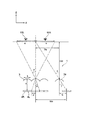
以下、本発明実施形態に係る表示装置及びその駆動方法、端末装置及び表示パネルについて、添付の図面を参照して具体的に説明する。まず、本発明の第1実施形態に係る表示装置及びその駆動方法、端末装置及び表示パネルについて説明する。図1は本発明の第1実施形態に係る表示装置を示す上面図であり、特に画素の電気的な接続と画像分離手段であるレンチキュラレンズとの関係を示す。図2は本実施形態に係る表示装置を示す断面図であり、図3は本実施形態に係る表示装置の画素を示す上面図であり、図4は本実施形態に係る端末装置を示す斜視図である。 Hereinafter, a display device, a driving method thereof, a terminal device, and a display panel according to embodiments of the present invention will be specifically described with reference to the accompanying drawings. First, a display device, a driving method thereof, a terminal device, and a display panel according to a first embodiment of the present invention will be described. FIG. 1 is a top view showing a display device according to the first embodiment of the present invention, and particularly shows the relationship between electrical connection of pixels and a lenticular lens as image separation means. 2 is a cross-sectional view illustrating the display device according to the present embodiment, FIG. 3 is a top view illustrating pixels of the display device according to the present embodiment, and FIG. 4 is a perspective view illustrating the terminal device according to the present embodiment. It is.
図1及び図2に示すように、本第1実施形態に係る表示装置は、電気光学素子として液晶分子を利用した表示パネル2にレンチキュラレンズ3を具備した立体表示用の表示装置1である。レンチキュラレンズ3は、表示パネル2の表示面側、すなわち使用者側に配置されている。
As shown in FIGS. 1 and 2, the display device according to the first embodiment is a
表示パネル2は、各1個の左眼用画素4L及び右眼用画素4Rからなる表示単位としての画素対がマトリクス状に設けられた視点数2なる立体表示用の表示パネルである。なお、本実施形態においては、左眼用画素4L及び右眼用画素4Rを総称して画素4とも呼称する。レンチキュラレンズ3は多数のシリンドリカルレンズ3aが一次元配列したレンズアレイである。シリンドリカルレンズ3aはかまぼこ状の凸部を有する一次元レンズである。その延伸方向、すなわち長手方向は、表示面内において配列方向と直交する方向となっている。シリンドリカルレンズ3aは延伸方向にはレンズ効果を持たず、その直交方向である配列方向にのみレンズ効果を有する。これにより、レンチキュラレンズ3はシリンドリカルレンズ3aの配列方向にのみレンズ効果を有する一次元レンズアレイとなっている。そして、シリンドリカルレンズ3aの配列方向は、左眼用画素4L及び右眼用画素4Rが繰り返し配列される方向に設定されている。なおシリンドリカルレンズ3aは、前述の表示単位と対応して配置されている。
The
シリンドリカルレンズ3aは、前述のようにその延伸方向と直交する方向にのみレンズ効果を有する。そして、本実施形態においては、このレンズ効果を有する方向が、左眼用画素4L及び右眼用画素4Rが繰り返し配列される方向と一致している。この結果、シリンドリカルレンズ3aは、左眼用画素4Lの光と右眼用画素4Rの光を異なる方向に分離可能な光線分離手段として作用する。これにより、レンチキュラレンズ3は、各表示単位の左眼用画素4Lが表示する画像と、各表示単位の右眼用画素4Rが表示する画像を、異なる方向に分離することができる。すなわち、レンチキュラレンズ3は、画像分離手段、画像振分手段として作用する光学部材である。なお、シリンドリカルレンズ3aの焦点距離は、シリンドリカルレンズ3aの主点、すなわちレンズの頂点と、画素面、すなわち左眼用画素4L又は右眼用画素4Rが配置された面との間の距離に設定されている。
As described above, the
なお、本明細書においては、便宜上、以下のようにXYZ直交座標系を設定する。左眼用画素4L及び右眼用画素4Rが繰り返し配列される方向において、右眼用画素4Rから左眼用画素4Lに向かう方向を+X方向とし、その反対方向を−X方向とする。+X方向及び−X方向を総称してX軸方向という。また、シリンドリカルレンズ3aの長手方向をY軸方向とする。更に、X軸方向及びY軸方向の双方に直交する方向をZ軸方向とし、このZ軸方向のうち、左眼用画素4L又は右眼用画素4Rが配置された面からレンチキュラレンズ3に向かう方向を+Z方向とし、その反対方向を−Z方向とする。+Z方向は前方、すなわち、使用者に向かう方向であり、使用者は表示パネル2の+Z側の面を視認することになる。そして、+Y方向は、右手座標系が成立する方向とする。すなわち、人の右手の親指を+X方向、人差指を+Y方向に向けたとき、中指は+Z方向を向くようにする。
In this specification, for convenience, an XYZ orthogonal coordinate system is set as follows. In the direction in which the left-
上述の如くXYZ直交座標系を設定すると、シリンドリカルレンズ3aの配列方向はX軸方向となり、左眼用の画像と右眼用の画像はX軸方向に沿って分離されることになる。また、左眼用画素4L及び右眼用画素4Rからなる表示単位がY軸方向に一列に配列される。X軸方向における画素対の配列周期はシリンドリカルレンズの配列周期と略等しくなっている。一つのシリンドリカルレンズ3aには、表示単位がY軸方向に配列した列が対応して配置されている。
When the XYZ orthogonal coordinate system is set as described above, the arrangement direction of the
表示パネル2においては、TFT基板2aと対向基板2bとが微小な間隙を設定して配置されており、この間隙に液晶層5LCが配置されている。液晶層5LCは例えば、透過型のTNモードとなるように構成されている。TFT基板2aは表示パネル2の−Z方向側に配置され、対向基板2bは+Z方向側に配置されている。すなわち、対向基板2bの更に+Z方向側にレンチキュラレンズ3が配置されている。
In the
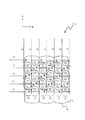
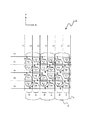
表示パネル2は薄膜トランジスタ(Thin Film Transistor:TFT)を有するアクティブマトリクス型の表示パネルである。薄膜トランジスタは各画素に表示信号を伝送するためのスイッチとして作用し、このスイッチを操作するのは、各スイッチのゲートに接続されたゲート線を流れるゲート信号である。本発明においては、TFT基板2aの内側の面、すなわち+Z方向側の面に、行方向、すなわちX軸方向に延伸するゲート線G1乃至G5が配置されている。なおゲート線G1乃至G5を総称してゲート線Gとも呼称する。更に、TFT基板2aの同じ面には、列方向、すなわちY軸方向に延伸するデータ線D1乃至D7が配置されている。データ線D1乃至D7を総称してデータ線Dとも呼称する。データ線は薄膜トランジスタに表示データ信号を供給する役割を果たす。本実施形態においては、ゲート線GはX軸方向に延伸し、Y軸方向に複数配列している。また、データ線Dは屈曲しているものの、複数回の屈曲を経て延伸する方向はY軸方向であり、X軸方向に複数配列している。そして、ゲート線とデータ線の交点近傍に、画素(左眼用画素4L又は右眼用画素4R)が配置されている。特に図1においては、画素のゲート線及びデータ線との接続関係を明確にするため、例えばゲート線G3とデータ線D2に接続された画素をP32と表記している。すなわち、Pの次の数字がゲート線のGの後の数字であり、更にその次の数字がデータ線のDの後の数字である。
The
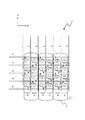
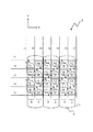
図1及び図3に示すように、画素4には画素電極4PIX、画素薄膜トランジスタ4TFT、蓄積容量4CSが配置されている。画素薄膜トランジスタ4TFTはMOS型の薄膜トランジスタであり、ソース電極又はドレイン電極の一方がコンタクトホール4CONTを介してデータ線Dに接続され、他方が画素電極4PIXと蓄積容量4CSの一方の電極に接続される。本発明においては、画素電極が接続された方の電極をソース電極、信号線に接続された方の電極をドレイン電極と呼称するものと定める。そして、画素薄膜トランジスタ4TFTのゲート電極は、ゲート線Gに接続される。蓄積容量4CSの他方の電極には、蓄積容量線CSが接続されている。更に、対向基板の内側には共通電極4COMが形成され、画素電極4PIXとの間で画素容量4CLCが形成される。また、図示していないが、対向基板の内側に画素の開口部以外を覆う遮光層が形成されていてもよい。本実施形態においては「遮光部」という表現を使用するが、これは特にこの遮光層に限定するものではなく、光を通さない部分を指すものである。なお、図3においては、各構成要素の大きさや縮尺は、図の視認性を確保するため、適宜変更して記載してある。また、画素4の構造は、左眼用画素4L及び右眼用画素4Rに対して共通である。また、図1においては、各画素のゲート線及びデータ線に対する接続関係を示すため、図3における薄膜トランジスタ及び画素電極を抽出して示している。
As shown in FIGS. 1 and 3, the
画素薄膜トランジスタ4TFTは、半導体として多結晶シリコンを使用したポリシリコン薄膜トランジスタを使用している。多結晶シリコンは一例では、微量のホウ素を含むP型半導体である。すなわち、画素薄膜トランジスタ4TFTは、ソース電極又はドレイン電極の電位よりもゲート電極の電位の方がローレベルとなった場合に、ソース電極とドレイン電極との間が導通状態となる所謂PMOS型の薄膜トランジスタである。 The pixel thin film transistor 4TFT uses a polysilicon thin film transistor using polycrystalline silicon as a semiconductor. In one example, polycrystalline silicon is a P-type semiconductor containing a small amount of boron. That is, the pixel thin film transistor 4TFT is a so-called PMOS type thin film transistor in which a conductive state is established between the source electrode and the drain electrode when the potential of the gate electrode becomes lower than the potential of the source electrode or the drain electrode. is there.
ポリシリコン薄膜トランジスタは一例では、TFT基板2a上に酸化シリコン層を形成した後でアモルファスシリコン層を形成し、このアモルファスシリコン層を多結晶化してポリシリコン薄膜を形成する。多結晶化する手段としては、熱アニール法やレーザアニール法が用いられるが、特にエキシマレーザ等のレーザを使用したレーザアニール法は、ガラス基板の温度上昇を最小限に留めた上でシリコン層のみを加熱多結晶化することができるため、融点の低い無アルカリガラス等を使用することができる。これにより、低コスト化が可能となるため、低温ポリシリコンと称して良く用いられている。なお、このアニール工程を省くことにより、アモルファスシリコン薄膜トランジスタを実現することもできる。
In an example of the polysilicon thin film transistor, an amorphous silicon layer is formed after forming a silicon oxide layer on the
次に、シリコン層の上にゲート絶縁層としての酸化シリコン層を形成し、適宜パターニングする。この過程で、シリコン薄膜の半導体層として使用する部分以外の領域にイオンをドーピングして、導体化することが好ましい。パターニングの手法としては、感光性レジストを使用する光パターニングの手法が適用できる。一例では、感光性レジストをスピンコートした後に、ステッパ等の露光機で光を部分照射し、現像工程を経て、パターンを残す部分にのみ感光性レジストの膜を残す。その後、ドライエッチング等により感光性レジストの膜が残存しない領域のシリコン層を除去し、最後に感光性レジストの膜を剥離する。 Next, a silicon oxide layer as a gate insulating layer is formed on the silicon layer, and is appropriately patterned. In this process, it is preferable that a region other than the portion used as the semiconductor layer of the silicon thin film is doped with ions to make a conductor. As a patterning technique, an optical patterning technique using a photosensitive resist can be applied. In one example, after the photosensitive resist is spin-coated, light is partially irradiated with an exposure machine such as a stepper, and the film of the photosensitive resist is left only in the portion where the pattern is left after the development process. Thereafter, the silicon layer in a region where the photosensitive resist film does not remain is removed by dry etching or the like, and finally the photosensitive resist film is peeled off.
次に、ゲート電極となるアモルファスシリコン層とタングステンシリサイド層を成膜し、ゲート電極等を形成する。このとき、ゲート電極が接続するゲート線や、蓄積容量線も同様に形成してもよい。次に、酸化シリコン層と窒化シリコン層を形成し、適宜パターニングした後に、アルミニウム層とチタン層を成膜し、ソース電極及びドレイン電極を形成する。このとき、データ線を同時に形成してもよい。 Next, an amorphous silicon layer and a tungsten silicide layer to be a gate electrode are formed, and a gate electrode and the like are formed. At this time, a gate line to which the gate electrode is connected and a storage capacitor line may be formed in the same manner. Next, after a silicon oxide layer and a silicon nitride layer are formed and appropriately patterned, an aluminum layer and a titanium layer are formed, and a source electrode and a drain electrode are formed. At this time, the data lines may be formed simultaneously.
次に窒化シリコン層を成膜し、適宜パターニングした後にITO等の透明電極を成膜、パターニングすることにより、画素電極を形成する。これにより、薄膜トランジスタを有する画素構造を形成することができる。なお、この薄膜トランジスタを用いて、ゲート線やデータ線、蓄積容量線を駆動する回路を同時に形成することもできる。 Next, after forming a silicon nitride layer and appropriately patterning it, a transparent electrode such as ITO is formed and patterned to form a pixel electrode. Thereby, a pixel structure having a thin film transistor can be formed. Note that a circuit for driving a gate line, a data line, or a storage capacitor line can be formed at the same time by using the thin film transistor.
図3は、本実施形態における画素を4個分示したものである。本実施形態においては、ゲート線G及び蓄積容量線CSは薄膜トランジスタ4TFTのゲート電極と同層で形成されている。また、シリコン層4SIと蓄積容量線CSとの間で、蓄積容量4CSが形成されている。前述のように、シリコン層4SIはコンタクトホール4CONTを介してデータ線Dに接続されるが、画素4において画素薄膜トランジスタ4TFT以外に設けられたもう一つのコンタクトホール4CONTは、蓄積容量4CSにおけるシリコン層4SIと画素電極4PIXを電気的に接続するためのものである。
FIG. 3 shows four pixels in this embodiment. In the present embodiment, the gate line G and the storage capacitor line CS are formed in the same layer as the gate electrode of the thin film transistor 4TFT. A storage capacitor 4CS is formed between the silicon layer 4SI and the storage capacitor line CS. As described above, the silicon layer 4SI is connected to the data line D via the contact hole 4CONT, but the other contact hole 4CONT provided in the
なお、本図においては、コンタクトホール4CONTは黒塗りで示し、画素電極4PIXは点線で、またシリコン層4SIは太線で、夫々の形状を示している。 In this figure, the contact hole 4CONT is shown in black, the pixel electrode 4PIX is shown as a dotted line, and the silicon layer 4SI is shown as a thick line, showing the respective shapes.
そして、本発明においては「隣接画素対」という表現を使用するが、これは特に、ゲート線を挟み配置された二つの画素が、この画素間に配置されたゲート線に接続された状態において使用するものとする。すなわち、隣接画素対を構成する画素は、この画素間に配置されたゲート線により、制御される。図3においては、左側の二つの画素が、隣接画素対4PAIRを構成する。 In the present invention, the expression “adjacent pixel pair” is used, which is particularly used when two pixels arranged with a gate line interposed therebetween are connected to a gate line arranged between the pixels. It shall be. That is, the pixels constituting the adjacent pixel pair are controlled by the gate lines arranged between the pixels. In FIG. 3, the two pixels on the left form an adjacent pixel pair 4PAIR.
更に、隣接画素対4PAIRを構成する各画素は、夫々異なるデータ線に接続される。図3の左側の隣接画素対4PAIRにおいては、−Y方向側の画素4は−X方向側に配置されたデータ線Dに接続され、+Y方向側の画素4は+X方向側に配置されたデータ線に接続されている。
Further, each pixel constituting the adjacent pixel pair 4PAIR is connected to a different data line. In the adjacent pixel pair 4PAIR on the left side of FIG. 3, the
そして、ゲート線Gの延伸方向、すなわちX軸方向に隣り合う隣接画素対4PAIRは、共通のゲート線Gに接続されず、異なるゲート線Gに接続されている。これは、隣接画素対4PAIRが、X軸方向においては、Y軸方向に画素一つ分だけずれた状態で隣り合っているからである。このように配置することにより、必要な配線数を最小限に抑えることができるため、開口率の向上が可能となる。 The adjacent pixel pair 4PAIR adjacent in the extending direction of the gate line G, that is, the X-axis direction, is not connected to the common gate line G, but is connected to different gate lines G. This is because the adjacent pixel pair 4PAIR is adjacent in the X-axis direction while being shifted by one pixel in the Y-axis direction. By arranging in this way, the necessary number of wirings can be minimized, so that the aperture ratio can be improved.
なお、本実施形態においては、図3に示す4個の画素がX軸方向及びY軸方向に繰り返し配置されていることになる。 In the present embodiment, the four pixels shown in FIG. 3 are repeatedly arranged in the X-axis direction and the Y-axis direction.
ここで再度図1を参照して、画素の配置関係を確認する。まず、画素P31と画素P32から構成される隣接画素対に着目する。説明の都合上、この隣接画素対の表記を(P31、P32)とすることにする。すると、隣接画素対(P31、P32)に対し、+X方向には、隣接画素対(P22、P23)が隣り合っている。隣接画素対(P22、P23)はゲート線G2を共通のゲート線としている。ここで、「隣接画素対がゲート線G2を共通のゲート線とする」という表現は、隣接画素対を構成する各画素は、ゲート線G2、すなわちこの画素間に配置されたゲート線に接続され、制御されることを意味する。隣接画素対(P31、P32)はゲート線G3を共通のゲート線とするので、隣接画素対(P31、P32)と隣接画素対(P22、P23)は、夫々異なるゲート線を共通のゲート線としている。ちなみに、夫々の共通ゲート線は隣接の関係にある。 Here, referring to FIG. 1 again, the pixel arrangement relationship is confirmed. First, attention is paid to an adjacent pixel pair composed of the pixel P31 and the pixel P32. For convenience of explanation, the notation of the adjacent pixel pair is (P31, P32). Then, the adjacent pixel pair (P22, P23) is adjacent to the adjacent pixel pair (P31, P32) in the + X direction. The adjacent pixel pair (P22, P23) uses the gate line G2 as a common gate line. Here, the expression “the adjacent pixel pair uses the gate line G2 as a common gate line” means that each pixel constituting the adjacent pixel pair is connected to the gate line G2, that is, the gate line disposed between the pixels. Mean to be controlled. Since the adjacent pixel pair (P31, P32) uses the gate line G3 as a common gate line, the adjacent pixel pair (P31, P32) and the adjacent pixel pair (P22, P23) use different gate lines as a common gate line. Yes. Incidentally, the common gate lines are adjacent to each other.
なお、隣接画素対(P31、P32)に対し、+X方向には、隣接画素対(P42、P43)も隣り合って配置されている。両者の隣接画素対においても同様に、夫々異なるゲート線を共通のゲート線としている。 The adjacent pixel pair (P42, P43) is also arranged adjacent to the adjacent pixel pair (P31, P32) in the + X direction. Similarly, in both adjacent pixel pairs, different gate lines are common gate lines.
更に、隣接画素対(P22、P23)又は隣接画素対(P42、P43)に対し、+X方向には、隣接画素対(P33、P34)が配置されている。この隣接画素対(P33、P34)はゲート線G3を共通ゲート線としている点は、隣接画素対(P31、P32)と同様である。すなわち、画素1列毎に、同じゲート線を共通ゲート線とする隣接画素対が配置されていることになる。これは換言すれば、右眼用画素4Rを構成する隣接画素対に接続されたゲート線は、左眼用画素4Lを構成する隣接画素対には接続されないことになる。
Furthermore, with respect to the adjacent pixel pair (P22, P23) or the adjacent pixel pair (P42, P43), the adjacent pixel pair (P33, P34) is arranged in the + X direction. The adjacent pixel pair (P33, P34) is similar to the adjacent pixel pair (P31, P32) in that the gate line G3 is used as a common gate line. That is, adjacent pixel pairs having the same gate line as a common gate line are arranged for each pixel column. In other words, the gate line connected to the adjacent pixel pair constituting the
次に、再度図3を参照して、画素の構造を説明する。本実施形態においては、隣接画素対を構成する一方の画素のデータ線と接続される部分、すなわちドレイン電極は、隣接画素対の共通ゲート線よりも他方の画素側に配置されている。例えば、隣接画素対(P31、P32)に着目すると、画素P31のドレイン電極は、ゲート線G3よりも+Y方向に配置され、画素P32側に配置されている。換言すれば、薄膜トランジスタ4TFTのドレイン電極とソース電極が、ゲート線Gを跨いで配置されている。一般的に、薄膜トランジスタのLサイズはドレイン電極とソース電極が形成された方向におけるシリコン薄膜の長さを指し、Wサイズはこの直交方向におけるシリコン薄膜の幅を指す。なお、Lサイズはチャネル長、Wサイズ幅はチャネル幅とも呼称される。そこで本発明においては、ドレイン電極とソース電極が形成された方向をL方向とし、この直交報告をW方向とすると、本実施形態においては、薄膜トランジスタのW方向がゲート線の延伸方向と一致して配置されていることになる。更に、薄膜トランジスタのシリコン薄膜部は、データ線Dと重ねて配置されている。なお、薄膜トランジスタはシングルゲート構成である。また、LサイズよりWサイズの方が大きい。 Next, the structure of the pixel will be described with reference to FIG. 3 again. In the present embodiment, the portion connected to the data line of one pixel constituting the adjacent pixel pair, that is, the drain electrode is disposed on the other pixel side than the common gate line of the adjacent pixel pair. For example, when paying attention to the adjacent pixel pair (P31, P32), the drain electrode of the pixel P31 is disposed in the + Y direction with respect to the gate line G3, and is disposed on the pixel P32 side. In other words, the drain electrode and the source electrode of the thin film transistor 4TFT are disposed across the gate line G. In general, the L size of the thin film transistor indicates the length of the silicon thin film in the direction in which the drain electrode and the source electrode are formed, and the W size indicates the width of the silicon thin film in the orthogonal direction. The L size is also called the channel length, and the W size width is also called the channel width. Therefore, in the present invention, when the direction in which the drain electrode and the source electrode are formed is the L direction, and this orthogonal report is the W direction, in this embodiment, the W direction of the thin film transistor coincides with the extending direction of the gate line. Will be placed. Further, the silicon thin film portion of the thin film transistor is disposed so as to overlap the data line D. Note that the thin film transistor has a single gate structure. The W size is larger than the L size.
そして、隣接画素対を構成する各画素は、点対称の関係に配置されている。また、各隣接画素対は、平行移動の関係に配置されている。すなわち、各隣接画素対は、平行移動した状態で配置されている。なお、平行移動とは、点対称移動や線対称移動をせずに、単に中心位置を変更する移動を指す。 And each pixel which comprises an adjacent pixel pair is arrange | positioned at the point-symmetrical relationship. Each pair of adjacent pixels is arranged in a translational relationship. That is, each adjacent pixel pair is arranged in a translated state. Note that the parallel movement refers to movement that simply changes the center position without performing point-symmetrical movement or line-symmetrical movement.
また、各画素における表示領域、すなわち表示に使用される領域は、略台形状となっている。これに伴い、画素電極4PIXの形状も、略台形状となっている。また、隣接画素対は、略台形状の表示領域を有する二つの画素が、上底側を向かい合わせて配置されたものと表現することもできる。そして薄膜トランジスタ4TFTは、略台形状を有する画素の表示領域の上底側に配置され、隣接画素対を構成する各画素の上底間に配置されている。 The display area in each pixel, that is, the area used for display is substantially trapezoidal. Accordingly, the shape of the pixel electrode 4PIX is also substantially trapezoidal. The adjacent pixel pair can also be expressed as two pixels having a substantially trapezoidal display area arranged with the top and bottom sides facing each other. The thin film transistor 4TFT is disposed on the upper bottom side of the display area of the pixel having a substantially trapezoidal shape, and is disposed between the upper bottoms of the pixels constituting the adjacent pixel pair.
また、蓄積容量線CSは、ゲート線の延伸方向、すなわちX軸方向に隣接する各画素の蓄積容量を接続するように配置されている。X軸方向に隣接する各画素においては、Y軸方向における薄膜トランジスタの位置が異なるため、蓄積容量線CSはこれらを結ぶように屈曲して配置されている。なお、蓄積容量は薄膜トランジスタと同様、各画素において、略台形状を有する表示領域の上底側に配置されている。これにより、隣接画素対を構成する各画素の上底間に蓄積容量を効率的に配置することができ、開口率の更なる向上が可能となる。また、蓄積容量線CSはゲート線の延伸方向と直交して配置されていない。これは、ゲート線の延伸方向に分離効果を有する画像分離手段を設ける際に、非常に重要なポイントとなる。また、蓄積容量線CSはゲート線Gと同層に形成されている点も、後述のように、開口率を高める上で重要である。 Further, the storage capacitor line CS is arranged so as to connect the storage capacitors of the respective pixels adjacent in the extending direction of the gate line, that is, the X-axis direction. Since each pixel adjacent in the X-axis direction has a different position of the thin film transistor in the Y-axis direction, the storage capacitor line CS is bent and arranged so as to connect them. Note that the storage capacitor is arranged on the upper bottom side of the display area having a substantially trapezoidal shape in each pixel, like the thin film transistor. As a result, the storage capacitor can be efficiently arranged between the upper bases of the pixels constituting the adjacent pixel pair, and the aperture ratio can be further improved. Further, the storage capacitor line CS is not arranged orthogonal to the extending direction of the gate line. This is a very important point when providing image separation means having a separation effect in the extending direction of the gate line. Further, the fact that the storage capacitor line CS is formed in the same layer as the gate line G is also important for increasing the aperture ratio, as will be described later.
そして、蓄積容量線CSとデータ線Dとの交差部分は、前記データ線に沿うように配置されている。 The intersection of the storage capacitor line CS and the data line D is arranged along the data line.
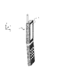
図4に示すように、本実施形態に係る端末装置は携帯電話9である。この携帯電話9には、前述の表示装置1が搭載されている。そして、表示装置1のX軸方向が携帯電話9の画面の横方向となり、表示装置1のY軸方向が携帯電話9の画面の縦方向となっている。
As shown in FIG. 4, the terminal device according to this embodiment is a
次に、本実施形態における画素構造とその効果について、より詳細に説明する。複数視点用表示装置において、高開口率化と高画質化を達成するためには、画素の縦開口率を横方向の位置によらず一定にしつつ、縦開口率を最大にする必要がある。なお、縦開口率とは、画像分離手段の画像分離方向(本実施形態ではX軸方向)と直交する方向(すなわちY軸方向)に延伸する線分を用いて、画素を切断した際のY軸方向の開口の高さを、Y軸方向の画素ピッチで除した値である。この縦開口率を、画像分離方向に依存せず一定にした上で、縦開口率を最大にする必要がある。 Next, the pixel structure and its effect in this embodiment will be described in more detail. In order to achieve high aperture ratio and high image quality in a multi-viewpoint display device, it is necessary to maximize the vertical aperture ratio while keeping the vertical aperture ratio of the pixels constant regardless of the position in the horizontal direction. The vertical aperture ratio is Y when a pixel is cut using a line segment extending in a direction (that is, the Y-axis direction) orthogonal to the image separation direction (X-axis direction in the present embodiment) of the image separation unit. This is a value obtained by dividing the height of the opening in the axial direction by the pixel pitch in the Y-axis direction. It is necessary to maximize the vertical aperture ratio while keeping the vertical aperture ratio constant regardless of the image separation direction.
まず、ゲート線及びデータ線の配置について考察すると、各画素の周囲にゲート線及びデータ線が配置されている方が好ましい。これにより、配線間のデッドスペースを削減して開口率の向上が可能となる。換言すれば、ゲート線同士又はデータ線同士が、間に画素を配置することなく隣接するのは避けた方がよい。これは、同種の配線同士が隣接してしまうと、ショートを防止するため配線間に間隔を設ける必要が発生し、この間隔がデッドスペースとなって開口率が低下するからである。 First, considering the arrangement of the gate line and the data line, it is preferable that the gate line and the data line are arranged around each pixel. Thereby, the dead space between wirings can be reduced and the aperture ratio can be improved. In other words, it is better to avoid that the gate lines or the data lines are adjacent to each other without disposing a pixel therebetween. This is because if the same kind of wirings are adjacent to each other, it is necessary to provide a space between the wires in order to prevent a short circuit, and this space becomes a dead space and the aperture ratio decreases.
なお、ゲート線の延伸方向と画像分離手段の画像分離方向との関係については、特に立体画像表示装置の場合には、少なくとも画像分離方向が表示装置の横方向となるように配置される。この時、ゲート線の延伸方向は従来同様、表示装置の横方向とするのが好ましい。通常、表示するデータは、ゲート線が横方向に延伸し、縦方向に配列するものとして入力される。したがって、90度回転した状態でゲート線を縦方向に延伸すると、入力データの縦横変換が必要になり、少なくとも1フレーム分の外部メモリが必要となって、表示装置の高コスト化を招いてしまうからである。すなわち、立体画像表示装置においては、画像分離手段の画像分離方向とゲート線の延伸方向を一致させるのが好ましい。 The relationship between the extending direction of the gate line and the image separating direction of the image separating means is arranged so that at least the image separating direction is the horizontal direction of the display device, particularly in the case of a stereoscopic image display device. At this time, it is preferable that the extending direction of the gate line is the horizontal direction of the display device as in the prior art. Usually, data to be displayed is input as gate lines extending in the horizontal direction and arranged in the vertical direction. Therefore, if the gate line is extended in the vertical direction while being rotated by 90 degrees, the vertical / horizontal conversion of the input data is required, and at least one frame of external memory is required, resulting in high cost of the display device. Because. That is, in the stereoscopic image display device, it is preferable that the image separation direction of the image separation means and the extending direction of the gate line are made to coincide.
更に、蓄積容量線CSは、画像分離方向に沿って延伸するように配置されるのが好ましい。これは、画像分離方向に沿って蓄積容量線を配列すると、画像分離手段により蓄積容量線の像が拡大されてしまい、表示画質を著しく劣化させてしまうからである。すなわち、画像分離方向に沿って配列する配線は極力削減するのが好ましく、本発明においてはデータ線のみを配列している。これにより、一層の画質の向上が可能となる。 Further, the storage capacitor line CS is preferably arranged so as to extend along the image separation direction. This is because if the storage capacitor lines are arranged along the image separation direction, the image of the storage capacitor lines is enlarged by the image separation means, and the display image quality is significantly deteriorated. That is, it is preferable to reduce the number of wirings arranged along the image separation direction as much as possible. In the present invention, only the data lines are arranged. As a result, the image quality can be further improved.
更に、データ線は、縦開口率を画像分離方向の位置によらず一定にするため、ゲート線の配列方向から屈曲させる必要がある。そして、縦開口率を限定する要因として、この屈曲した斜辺部の構造と、台形状開口における下底間の構造、及び上底間の構造が挙げられる。より具体的には、図3のA−A線に示すように、斜辺部を切断する縦線においては、斜辺部のY軸方向における高さと下底間の高さが縦開口率に影響する。また、図3のB−B線に示すように、TFT部を切断する縦線においては、上底間の高さと下底間の高さが縦開口率に影響する。 Further, the data line needs to be bent from the arrangement direction of the gate lines in order to make the vertical aperture ratio constant regardless of the position in the image separation direction. Factors that limit the vertical aperture ratio include the bent oblique side structure, the structure between the lower bases in the trapezoidal opening, and the structure between the upper bases. More specifically, as shown by the AA line in FIG. 3, in the vertical line that cuts the hypotenuse, the height of the hypotenuse in the Y-axis direction and the height between the bottom base affects the vertical aperture ratio. . Further, as shown by the line BB in FIG. 3, in the vertical line that cuts the TFT portion, the height between the upper bases and the height between the lower bases affect the vertical aperture ratio.
A−A線、B−B線のどちらにも共通するのは、下底間の高さである。そこでまず、この下底間の高さを最小にするための構造を検討する。前述のように、下底間には少なくともゲート線1本は配置する必要がある。そして下底間の高さを最小にするためには、構造物はこのゲート線1本に留めるのが好ましい。例えば下底間に薄膜トランジスタを配置すると、その分だけ下底間の高さが増大してしまうので好ましくない。特にA−A線においては、下底部が重複して配置されているため、下底間の高さが増大した際の影響が非常に大きい。下底間への構造物の配置は極力避けるべきである。また、蓄積容量線をゲート線と同層で形成する場合には、下底間に蓄積容量線を配置しない方が好ましい。これにより、下底間の高さを削減しつつ、かつ省プロセス化が実現できる。 What is common to both the AA line and the BB line is the height between the lower bases. Therefore, first, a structure for minimizing the height between the lower bases is examined. As described above, it is necessary to arrange at least one gate line between the lower bases. In order to minimize the height between the bottoms, it is preferable to keep the structure on this single gate line. For example, disposing a thin film transistor between the bottoms is not preferable because the height between the bottoms increases accordingly. In particular, in the AA line, since the lower bottom portion is overlapped, the influence when the height between the lower bottoms is increased is very large. The arrangement of structures between the bottoms should be avoided as much as possible. Further, when the storage capacitor line is formed in the same layer as the gate line, it is preferable not to arrange the storage capacitor line between the lower bases. Thereby, it is possible to reduce the process while reducing the height between the bottoms.
次に、A−A線における斜辺部の高さについて検討する。この斜辺部においては、配線を屈曲して配置しているため、屈曲した分だけ高さが大きくなる。例えば、Y軸方向に対する屈曲角をθとし、斜辺部の幅をWOBとすると、斜辺部の高さは、WOB/sinθとなる。例えば、θが30度の場合だと、斜辺部の高さは幅の2倍となる。このように、斜辺部の高さは幅の1/sinθ倍で影響を受けるので、斜辺部の幅を小さくするのは非常に重要である。 Next, the height of the hypotenuse on the line AA will be examined. Since the wiring is bent at this oblique side, the height is increased by the amount of bending. For example, if the bending angle with respect to the Y-axis direction is θ and the width of the oblique side is WOB, the height of the oblique side is WOB / sin θ. For example, when θ is 30 degrees, the height of the hypotenuse is twice the width. Thus, since the height of the hypotenuse is affected by 1 / sin θ times the width, it is very important to reduce the hypotenuse width.
斜辺部の幅を小さくするには、斜辺部に構造物を極力配置しないのが好ましい。例えば斜辺部に薄膜トランジスタを配置すると、その分だけ幅が増大し、1/sinθ倍で高さが増大してしまうので好ましくない。しかし前述のように、最低限1本のデータ線は配置する必要がある。また蓄積容量線をゲート線と同層で形成する場合には、特に蓄積容量線をデータ線と重ねて配置することもできる。この時には、蓄積容量線CSとデータ線Dとの交差部分は、前記データ線に沿うように配置されることになる。これにより、斜辺部の高さを削減でき、縦開口率の向上が可能となる。 In order to reduce the width of the hypotenuse part, it is preferable not to arrange a structure as much as possible in the hypotenuse part. For example, if a thin film transistor is disposed on the oblique side, the width increases accordingly, and the height increases by 1 / sin θ times, which is not preferable. However, as described above, it is necessary to arrange at least one data line. In the case where the storage capacitor line is formed in the same layer as the gate line, the storage capacitor line can be particularly arranged so as to overlap the data line. At this time, the intersection between the storage capacitor line CS and the data line D is arranged along the data line. Thereby, the height of the hypotenuse can be reduced, and the vertical aperture ratio can be improved.
最後に、B−B線における上底間の高さについて検討する。前述のように、下底間及び斜辺部には薄膜トランジスタを配置できなかったため、この上底間に配置する必要がある。そして、上底間の高さを低減するような配置が重要となる。図3を参照すると明らかであるが、上底間において最も高さを有する構造物は薄膜トランジスタである。そこで、この薄膜トランジスタの高さ、すなわちY軸方向に長さを低減するのが重要になる。 Finally, the height between the upper bases in the BB line will be examined. As described above, since the thin film transistor cannot be disposed between the lower bases and between the oblique sides, it must be disposed between the upper bases. And arrangement | positioning which reduces the height between upper bases becomes important. As is apparent from FIG. 3, the structure having the highest height between the top and bottom is a thin film transistor. Therefore, it is important to reduce the height of the thin film transistor, that is, the length in the Y-axis direction.
本実施形態においては、薄膜トランジスタのドレイン電極とソース電極が、ゲート線Gを跨いで配置されている。換言すれば、隣接画素対を構成する一方の画素のデータ線と接続される部分は、隣接画素対の共通ゲート線よりも他方の画素側に配置されている。これにより、特に薄膜トランジスタのWサイズがLサイズよりも大きい場合には、効率良く薄膜トランジスタを配置することができる。 In the present embodiment, the drain electrode and the source electrode of the thin film transistor are disposed across the gate line G. In other words, the portion connected to the data line of one pixel constituting the adjacent pixel pair is disposed on the other pixel side than the common gate line of the adjacent pixel pair. Thereby, especially when the W size of the thin film transistor is larger than the L size, the thin film transistor can be arranged efficiently.
一方で、薄膜トランジスタのW方向をゲート線の延伸方向と平行に配置すると、薄膜トランジスタのドレイン電極とソース電極が、ゲート線を跨いで配置するのは困難になる。その結果、薄膜トランジスタを効率良く配置するのは困難になる。特に、ゲート線と蓄積容量線を同層に形成した場合には、ゲート線と蓄積容量線の間隔を設ける必要が発生するため、更に効率は低下してしまう。 On the other hand, when the W direction of the thin film transistor is arranged in parallel with the extending direction of the gate line, it is difficult to arrange the drain electrode and the source electrode of the thin film transistor across the gate line. As a result, it is difficult to efficiently arrange the thin film transistors. In particular, when the gate line and the storage capacitor line are formed in the same layer, it is necessary to provide an interval between the gate line and the storage capacitor line, and the efficiency further decreases.
更に、本実施形態においては、隣接画素対を構成する二つの画素の薄膜トランジスタが、X軸方向において異なる位置に配置されている。これにより、ドレイン電極とソース電極がゲート線を跨いで配置するレイアウトを容易に実現できる。そして、隣接画素対を構成する各画素は、点対称の関係に配置されている。この点対称配置により、各画素のレイアウトを容易にすることができ、設計工数の削減が可能となる。 Further, in the present embodiment, the thin film transistors of the two pixels constituting the adjacent pixel pair are arranged at different positions in the X-axis direction. Thereby, a layout in which the drain electrode and the source electrode are arranged across the gate line can be easily realized. And each pixel which comprises an adjacent pixel pair is arrange | positioned at the point-symmetrical relationship. With this point-symmetric arrangement, the layout of each pixel can be facilitated, and the design man-hour can be reduced.
なお、本実施形態に示すように、蓄積容量線は薄膜トランジスタの近傍に配置するのが、蓄積容量を形成する上で最も効率が高い。これは、蓄積容量が、薄膜トランジスタのドレイン電極に接続された電極と、蓄積容量線に接続された電極との間で形成されることから明らかである。 Note that, as shown in the present embodiment, the storage capacitor line is arranged in the vicinity of the thin film transistor for the highest efficiency in forming the storage capacitor. This is apparent from the fact that the storage capacitor is formed between the electrode connected to the drain electrode of the thin film transistor and the electrode connected to the storage capacitor line.
更に、薄膜トランジスタのシリコン薄膜部をデータ線Dと積層して配置することにより、無駄なスペースを削減した上で、蓄積容量などのスペースとして活用することができる。 Furthermore, by disposing the silicon thin film portion of the thin film transistor so as to be laminated with the data line D, it is possible to use it as a space such as a storage capacitor while reducing a useless space.
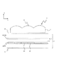
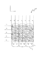
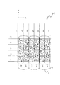
次に、上述の如く構成された本実施形態に係る表示装置の駆動方法、すなわち表示動作について説明する。図5は、本実施形態に係る表示装置において、各画素の極性を示す上面図である。本実施形態においては、表示装置1はドット反転駆動を用いて駆動される。ドット反転駆動は、データ線1本毎に各々伝送される表示データの極性が基準電位に対して反転され、かつゲート線1本毎に各々データ線を伝送される表示データの極性が反転され、かつフレーム毎に極性が反転される駆動方法である。ドット反転駆動は1H1V反転駆動とも称される。これは、水平方向(H方向)に配列するデータ線1本毎、また垂直方向(V方向)に配列するゲート線1本毎に極性が反転しているからである。
Next, a driving method of the display device according to the present embodiment configured as described above, that is, a display operation will be described. FIG. 5 is a top view showing the polarity of each pixel in the display device according to the present embodiment. In the present embodiment, the
図5を参照して具体的に説明するが、これはあるフレームにおいて、ドット反転駆動の結果実現される各画素の極性を示したものである。まず、ゲート線G1が選択されると、データ線D1には正極性の表示データが伝送され、画素P11には正極性の電圧が書き込まれる。またデータ線D2には負極性の表示データが伝送される。同様に、データ線D3、D5、D7には正極性の表示データが伝送され、データ線D4、D6には負極性の表示データが伝送される。次にゲート線G2が選択された場合には、データ線の極性が全て反転される。すなわち、データ線D1、D3、D5、D7には負極性の表示データが伝送され、データ線D2、D4、D6には正極性の表示データが伝送される。以降、ゲート線G3、G5の選択時は、ゲート線G1の選択時と同様であり、ゲート線G4の選択時は、ゲート線G2の選択時と同様である。そして、このフレームが終了すると、次のフレームにおいては、更に極性反転が実行される。すなわち、ゲート線G1、G3、G5選択時においては、データ線D1、D3、D5、D7に負極性の表示データが伝送され、データ線D2、D4、D6に正極性の表示データが伝送される。また、ゲート線G2、G4選択時においては、データ線D1、D3、D5、D7に正極性の表示データが伝送され、データ線D2、D4、D6に負極性の表示データが伝送される。 This will be described in detail with reference to FIG. 5, which shows the polarity of each pixel realized as a result of dot inversion driving in a certain frame. First, when the gate line G1 is selected, positive display data is transmitted to the data line D1, and a positive voltage is written to the pixel P11. Further, negative display data is transmitted to the data line D2. Similarly, positive display data is transmitted to the data lines D3, D5, and D7, and negative display data is transmitted to the data lines D4 and D6. Next, when the gate line G2 is selected, all the polarities of the data lines are inverted. That is, negative display data is transmitted to the data lines D1, D3, D5, and D7, and positive display data is transmitted to the data lines D2, D4, and D6. Thereafter, the selection of the gate lines G3 and G5 is the same as the selection of the gate line G1, and the selection of the gate line G4 is the same as the selection of the gate line G2. When this frame ends, polarity inversion is further performed in the next frame. That is, when the gate lines G1, G3, and G5 are selected, negative display data is transmitted to the data lines D1, D3, D5, and D7, and positive display data is transmitted to the data lines D2, D4, and D6. . When the gate lines G2 and G4 are selected, positive display data is transmitted to the data lines D1, D3, D5, and D7, and negative display data is transmitted to the data lines D2, D4, and D6.
なお、ドット反転駆動における基準電位としては、画素電極に対向する共通電極の電位を挙げることができる。しかし厳密には、共通電極電位は薄膜トランジスタのフィードスルーの影響を低減するために、DCオフセットを印加することが多く、基準電位とは異なるものである。 Note that the reference potential in the dot inversion driving can be the potential of the common electrode facing the pixel electrode. However, strictly speaking, the common electrode potential is often applied with a DC offset in order to reduce the influence of the feedthrough of the thin film transistor, and is different from the reference potential.
ここで、右眼用画素4Rから構成される画素群に着目すると、Y軸方向には異極性の画素が配列するものの、X軸方向には同極性の画素が配列している。左眼用画素4Lから構成される画素群においても同様である。すなわち、各視点においてはライン反転効果が実現されていることになり、他のフレーム反転効果等と比較して高画質化が可能となる。
Here, paying attention to the pixel group composed of the right-
本実施形態においては、奇数番目のゲート線が右眼用画素に接続され、偶数番目のゲート線が左眼用画素に接続されている。このように、ゲート線によって左眼用画素又は右眼用画素が選択できる効果は非常に大きい。例えば、左右画像が水平方向に並べて配置されたサイドバイサイド形式の表示データが入力される場合には、表示データ1行分に対してゲート線2本分を順次走査して対応することができる。これにより、入力データの一時的な保存に必要なメモリを削減することが可能となり、低コスト化が実現できる。すなわち、本実施形態においては、サイドバイサイド形式の入力に対しては、ゲート線を順次走査する駆動方法を好適に組み合わせることができる。 In the present embodiment, odd-numbered gate lines are connected to the right-eye pixels, and even-numbered gate lines are connected to the left-eye pixels. Thus, the effect that the left-eye pixel or the right-eye pixel can be selected by the gate line is very large. For example, when side-by-side display data in which left and right images are arranged in a horizontal direction is input, it is possible to sequentially scan two gate lines for one row of display data. As a result, it is possible to reduce the memory required for temporary storage of input data, thereby realizing cost reduction. That is, in the present embodiment, a driving method for sequentially scanning the gate lines can be suitably combined with side-by-side input.
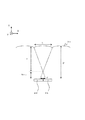
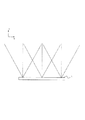
ここで、本実施形態における立体画像表示装置の構成の一例と、レンチキュラレンズが画像振分手段として作用するための条件について詳述する。本実施形態においては、画像振分手段は、左眼用画素と右眼用画素が配列する第1の方向、すなわちX軸方向に沿って、各画素から出射した光を相互に異なる方向に振り分けなければならない。そこでまず、画像振分効果を最大限に発揮する場合について、図6を使用して説明する。 Here, an example of the configuration of the stereoscopic image display apparatus in the present embodiment and conditions for the lenticular lens to act as the image distribution means will be described in detail. In this embodiment, the image distribution means distributes the light emitted from each pixel in different directions along the first direction in which the left-eye pixels and the right-eye pixels are arranged, that is, the X-axis direction. There must be. First, a case where the image distribution effect is maximized will be described with reference to FIG.
レンチキュラレンズ3の主点、すなわち頂点と画素との間の距離をHとし、レンチキュラレンズ3の屈折率をnとし、レンズピッチをLとする。また、左眼用画素4L又は右眼用画素4Rの各1個のピッチをPとする。このとき、各1個の左眼用画素4L及び右眼用画素4Rからなる表示画素の配列ピッチは2Pとなる。
The distance between the principal point of the
また、レンチキュラレンズ3と観察者との間の距離を最適観察距離ODとし、この距離ODにおける画素の拡大投影像の周期、すなわち、レンズから距離ODだけ離れレンズと平行な仮想平面上における左眼用画素4L及び右眼用画素4Rの投影像の幅の周期を夫々eとする。更に、レンチキュラレンズ3の中央に位置するシリンドリカルレンズ3aの中心から、X軸方向におけるレンチキュラレンズ3の端に位置するシリンドリカルレンズ3aの中心までの距離をWLとし、反射型液晶表示パネル2の中心に位置する左眼用画素4Lと右眼用画素4Rからなる表示画素の中心と、X軸方向における表示パネル2の端に位置する表示画素の中心との間の距離をWPとする。更にまた、レンチキュラレンズ3の中央に位置するシリンドリカルレンズ3aにおける光の入射角及び出射角を夫々α及びβとし、X軸方向におけるレンチキュラレンズ3の端に位置するシリンドリカルレンズ3aにおける光の入射角及び出射角を夫々γ及びδとする。更にまた、距離WLと距離WPとの差をCとし、距離WPの領域に含まれる画素数を2m個とする。
The distance between the
シリンドリカルレンズ3aの配列ピッチLと画素の配列ピッチPとは相互に関係しているため、一方に合わせて他方を決めることになるが、通常、表示パネルに合わせてレンチキュラレンズを設計することが多いため、画素の配列ピッチPを定数として扱う。また、レンチキュラレンズ3aの材料を選択することにより、屈折率nが決定される。これに対して、レンズと観察者との間の観察距離OD、及び観察距離ODにおける画素拡大投影像の周期eは所望の値を設定する。これらの値を使用して、レンズの頂点と画素との間の距離H及びレンズピッチLを決定する。スネルの法則と幾何学的関係より、下記数式1乃至6が成立する。また、下記数式7乃至9が成立する。
Since the arrangement pitch L of the
[数1]
n×sinα=sinβ
[Equation 1]
n × sin α = sin β
[数2]
OD×tanβ=e
[Equation 2]
OD × tan β = e
[数3]
H×tanα=P
[Equation 3]
H × tan α = P
[数4]
n×sinγ=sinδ
[Equation 4]
n × sin γ = sin δ
[数5]
H×tanγ=C
[Equation 5]
H × tan γ = C
[数6]
OD×tanδ=WL
[Equation 6]
OD × tan δ = WL
[数7]
WP−WL=C
[Equation 7]
WP-WL = C
[数8]
WP=2×m×P
[Equation 8]
WP = 2 × m × P
[数9]
WL=m×L
前述のようにまず画像振分効果を最大限に発揮する場合について考えるが、これはレンチキュラレンズの頂点と画素との間の距離Hを、レンチキュラレンズの焦点距離fと等しく設定した場合である。これにより、下記数式10が成立する。そして、レンズの曲率半径をrとすると、曲率半径rは下記数式11により求まる。
[Equation 9]
WL = m × L
First, consider the case where the image distribution effect is maximized as described above. This is the case where the distance H between the vertex of the lenticular lens and the pixel is set equal to the focal length f of the lenticular lens. As a result, the following
[数10]
f=H
[Equation 10]
f = H
[数11]
r=H×(n−1)/n
上記のパラメータについてまとめると、画素の配列ピッチPは表示パネルにより決定される値であり、観察距離OD及び画素拡大投影像の周期eは表示装置の設定により決定される値である。屈折率nはレンズ等の材質により決定される。そして、これらから導出されるレンズの配列ピッチL、レンズと画素との距離Hは、各画素からの光が観察面に投影される位置を決定するためのパラメータとなる。画像振分効果を変更するパラメータは、レンズの曲率半径rである。すなわち、レンズと画素との距離Hが固定の場合には、レンズの曲率半径を理想状態から変更すると、左右の画素の像がぼやけて、明確に分離しなくなる。すなわち、分離が有効となる曲率半径の範囲を求めれば良い。
[Equation 11]
r = H × (n−1) / n
Summarizing the above parameters, the pixel arrangement pitch P is a value determined by the display panel, and the observation distance OD and the period e of the enlarged pixel projection image are values determined by the setting of the display device. The refractive index n is determined by the material of the lens or the like. The lens arrangement pitch L and the lens-to-pixel distance H derived from these are parameters for determining the position at which the light from each pixel is projected onto the observation surface. The parameter for changing the image distribution effect is the radius of curvature r of the lens. That is, when the distance H between the lens and the pixel is fixed, if the radius of curvature of the lens is changed from the ideal state, the images of the left and right pixels are blurred and cannot be clearly separated. That is, it is only necessary to obtain a radius of curvature range in which separation is effective.
まず、レンズの分離作用が存在するための、曲率半径範囲の最小値を算出する。図7に示すように、分離作用が存在するためには、レンズピッチLを底辺とし焦点距離fを高さとする三角形と、画素ピッチPを底辺としH−fを高さとする三角形とにおいて、相似の関係が成立すればよい。これより、下記数式12が成立し、焦点距離の最小値fminを求めることができる。
First, the minimum value of the radius of curvature range for the lens separation action is calculated. As shown in FIG. 7, in order for the separation effect to exist, a triangle having a lens pitch L as a base and a focal length f as a height is similar to a triangle having a pixel pitch P as a base and Hf as a height. It is sufficient if the relationship is established. Thus, the following
[数12]
fmin=H×L/(L+P)
次に焦点距離から曲率半径を算出する。数式11を使用して、曲率半径の最小値rminは、下記数式13のように求めることができる。
[Equation 12]
fmin = H × L / (L + P)
Next, the radius of curvature is calculated from the focal length. Using Equation 11, the minimum value rmin of the radius of curvature can be obtained as
[数13]
rmin=H×L×(n−1)/(L+P)/n
次に、最大値を算出する。図8に示すように、分離作用が存在するためには、レンズピッチLを底辺とし焦点距離fを高さとする三角形と、画素ピッチPを底辺としf−Hを高さとする三角形とにおいて、相似の関係が成立すればよい。
[Equation 13]
rmin = H × L × (n−1) / (L + P) / n
Next, the maximum value is calculated. As shown in FIG. 8, in order for the separation effect to exist, a triangle having a lens pitch L as a base and a focal length f as a height is similar to a triangle having a pixel pitch P as a base and fH as a height. It is sufficient if the relationship is established.
これより、下記数式14が成立し、焦点距離の最大値fmaxを求めることができる。 Thus, the following formula 14 is established, and the maximum focal length fmax can be obtained.
[数14]
fmax=H×L/(L−P)
次に焦点距離から曲率半径を算出する。数式11を使用して、曲率半径の最小値rmaxは、下記数式15のように求めることができる。
[Formula 14]
fmax = H × L / (LP)
Next, the radius of curvature is calculated from the focal length. Using Equation 11, the minimum value rmax of the radius of curvature can be obtained as
[数15]
rmax=H×L×(n−1)/(L−P)/n
以上まとめると、レンズが画像振分効果を発揮するためには、レンズの曲率半径が数式13及び数式15により示される下記数式16の範囲に存在する必要がある。
[Equation 15]
rmax = H * L * (n-1) / (LP) / n
In summary, in order for the lens to exhibit the image distribution effect, the radius of curvature of the lens needs to be within the range of the following Expression 16 expressed by
[数16]
H×L×(n−1)/(L+P)/n≦r≦H×L×(n−1)/(L−P)/n
なお上記においては、左眼用画素と右眼用画素とを有する2視点の立体画像表示装置について説明したが、本発明はこれに限定されるものではない。例えば、N視点方式の表示装置に対して同様に適用することができる。この場合には、前述の距離WPの定義において、距離WPの領域に含まれる画素数を、2m個からN×m個に変更すればよい。
[Equation 16]
H × L × (n−1) / (L + P) / n ≦ r ≦ H × L × (n−1) / (LP) / n
In the above description, a two-viewpoint stereoscopic image display device having a left-eye pixel and a right-eye pixel has been described. However, the present invention is not limited to this. For example, the present invention can be similarly applied to an N-viewpoint display device. In this case, in the above-described definition of the distance WP, the number of pixels included in the area of the distance WP may be changed from 2m to N × m.
本実施形態の構成において、更なる高画質化を実現するためには、縦開口率を横方向の位置によらず、完全に一定とするのが好ましい。しかしながら、特に台形開口の斜辺部における頂点近傍では、遮光部の加工精度などにより、完全に縦開口率を一定にするのが難しい。そこで、本実施形態においては、図9及び図10に示すように、レンズの焦点を画素面からずらして配置することにより、この遮光部の加工精度に起因する影響を低減して、高画質化が可能となる。ここで、斜辺領域のX軸方向における幅をTWとすると、レンズの焦点を画素面からずらして配置した時の画素面におけるスポット径は、TW以上、2×TW以下の範囲にあることが好ましい。スポット径がTWの場合は、台形開口の斜辺と上底の交点、及び斜辺と下底の交点の影響を複合してぼかせる限界であり、これより大きく設定することが好ましい。そして、スポット径が2×TWの場合は、台形開口の斜辺と上底の交点のぼかし量を、斜辺と下底の交点の位置まで広げることができる。ただし、これよりぼかし量が大きくなると、レンズの分離性能が低下していくので好ましくない。したがって、下記の数式17又は数式18が成立する範囲にレンズ曲率を設定することが好ましい。
In the configuration of the present embodiment, in order to realize further higher image quality, it is preferable that the vertical aperture ratio be completely constant regardless of the position in the horizontal direction. However, especially in the vicinity of the apex of the oblique side of the trapezoidal opening, it is difficult to make the vertical aperture ratio completely constant due to the processing accuracy of the light shielding part. Therefore, in this embodiment, as shown in FIGS. 9 and 10, the influence of the processing accuracy of the light-shielding portion is reduced and the image quality is improved by disposing the focal point of the lens from the pixel surface. Is possible. Here, assuming that the width of the hypotenuse region in the X-axis direction is TW, the spot diameter on the pixel surface when the focal point of the lens is shifted from the pixel surface is preferably in the range of TW or more and 2 × TW or less. . When the spot diameter is TW, it is a limit that blurs the influence of the intersection of the oblique side and the upper base of the trapezoidal opening and the intersection of the oblique side and the lower base, and is preferably set larger than this. When the spot diameter is 2 × TW, the amount of blurring at the intersection of the oblique side of the trapezoidal opening and the upper base can be expanded to the position of the intersection of the oblique side and the lower base. However, if the amount of blurring is larger than this, it is not preferable because the lens separation performance deteriorates. Therefore, it is preferable to set the lens curvature within a range where the following
[数17]
H×L×(n−1)/(L+2×TW)/n≦r≦H×L×(n−1)/(L+TW)/n
[Equation 17]
H × L × (n−1) / (L + 2 × TW) / n ≦ r ≦ H × L × (n−1) / (L + TW) / n
[数18]
H×L×(n−1)/(L−TW)/n≦r≦H×L×(n−1)/(L−2×TW)/n
更に、図3のA−A線における斜辺及び下底部と、B−B線における上底部及び下底部を比較すると、B−B線が開口と遮光部との境界を横切るのは、1画素あたり上底と下底の2回であるのに対し、A−A線が横切るのは、1画素あたり上底と下底、及び斜辺部2回の合計4回となる。すなわち、遮光部を開口領域以外に形成した場合、この遮光部が設計値に対してより大きく形成されると、B−B線よりもA−A線における縦開口率が低下してしまうことになる。例えば、設計値に対して遮光部が片側ΔWOBだけ大きく形成される場合を考えると、B−B線における縦開口の高さは、2×ΔWOBだけ小さくなる。一方で、A−A線における縦開口の高さは、2×ΔWOB(1+1/sinθ)だけ小さくなる。ここで、角度θは前述のように、斜辺部のY軸方向に対する傾斜角である。
[Equation 18]
H × L × (n−1) / (L−TW) / n ≦ r ≦ H × L × (n−1) / (L−2 × TW) / n
Further, when comparing the hypotenuse and the lower base in the AA line in FIG. 3 with the upper and lower bases in the BB line, it is per pixel that the BB line crosses the boundary between the opening and the light shielding part. While the upper base and the lower base are two times, the line AA crosses a total of four times per pixel, that is, the upper base and the lower base and the hypotenuse part twice. That is, when the light shielding portion is formed in a region other than the opening region, if the light shielding portion is formed larger than the design value, the vertical aperture ratio in the AA line is lower than that in the BB line. Become. For example, considering the case where the light-shielding part is formed larger by one side ΔWOB than the design value, the height of the vertical opening in the BB line is reduced by 2 × ΔWOB. On the other hand, the height of the vertical opening along the AA line is reduced by 2 × ΔWOB (1 + 1 / sin θ). Here, as described above, the angle θ is an inclination angle of the hypotenuse with respect to the Y-axis direction.
そこで、特に遮光部が片側ΔWOBだけ大きく形成されることが予め判明している場合には、斜辺部における遮光部のY軸方向の長さを、2×ΔWOB/sinθだけ小さくしておくのも有効である。 Therefore, in particular, when it is known in advance that the light shielding portion is formed larger by one side ΔWOB, the length of the light shielding portion in the Y-axis direction at the oblique side portion may be reduced by 2 × ΔWOB / sin θ. It is valid.
なお上述の説明は、観察面に複数個の視点を設定し、その設定した各視点に向かって表示面の全ての表示単位から各視点用の画素の光が出射する方式のものである。この方式は、ある定めた視点に向かって、該当する視点の光を集めるため、集光方式とも呼称される。集光方式には、上述の2視点方式の立体表示装置や、更に視点数を増やした多視点方式の立体表示装置が分類される。図11に集光方式の概念図を示す。集光方式では観察者の眼に入射する光線を再現して表示する点が特徴的である。本発明は、このような集光方式に対して効果的に適用することができる。 In the above description, a plurality of viewpoints are set on the observation plane, and light of pixels for each viewpoint is emitted from all display units on the display plane toward the set viewpoints. This method is also referred to as a condensing method in order to collect light from a corresponding viewpoint toward a predetermined viewpoint. The two-viewpoint stereoscopic display device described above and the multi-viewpoint stereoscopic display device with an increased number of viewpoints are classified as the condensing method. FIG. 11 shows a conceptual diagram of the condensing method. The condensing method is characterized in that light rays incident on the observer's eyes are reproduced and displayed. The present invention can be effectively applied to such a condensing method.
更に、図12に示すように、空間像方式や空間像再生方式、空間像再現方式、空間像形成方式などと呼称される方式が提案されている。空間像方式は集光方式と異なり、特定の視点を設置しない。そして、空間の物体が発する光を再現するように表示する点が異なる。このような空間像方式には、インテグラルフォトグラフィ方式やインテグラルビデオグラフィ方式、インテグラルイメージング方式の立体表示装置が分類される。空間像方式においては、任意の場所に位置する観察者は、表示面全体で同一視点用の画素のみを視認することはない。しかしながら、同一視点用の画素が形成する所定の幅の領域が、複数種類存在することになる。この各領域においては、本発明は前述の集光方式と同様の効果を発揮できるため、空間像方式においても本発明を有効に適用することができる。 Furthermore, as shown in FIG. 12, a method called an aerial image method, an aerial image reproduction method, an aerial image reproduction method, an aerial image formation method, or the like has been proposed. Unlike the light collection method, the aerial image method does not set a specific viewpoint. And the point which displays so that the light which the object of space emits may be reproduced. As such a spatial image system, an integral photography system, an integral videography system, and an integral imaging system stereoscopic display device are classified. In the aerial image method, an observer located at an arbitrary place does not see only the pixels for the same viewpoint on the entire display surface. However, there are a plurality of types of regions having a predetermined width formed by pixels for the same viewpoint. In each of these regions, the present invention can exhibit the same effect as the above-described condensing method, and therefore the present invention can be effectively applied to the aerial image method.
なお、本発明においては、「視点」を「使用者が注視する表示領域上のある点(viewing point)」という意味ではなく、「表示装置を視認する位置(observation position)」や、「使用者の眼が位置すべき点又は領域」という意味で使用している。 In the present invention, “viewpoint” does not mean “viewing point on the display area where the user gazes”, but “viewing position of the display device (observation position)” or “user It is used to mean “a point or region where the eye of the eye should be located”.
本実施形態においては、説明を簡略化するため、ゲート線の本数、データ線の本数は、説明に必要な数に限定した。本発明はこれに限定されるものではなく、本発明の本質には影響を与えない。 In this embodiment, in order to simplify the description, the number of gate lines and the number of data lines are limited to the numbers necessary for the description. The present invention is not limited to this, and does not affect the essence of the present invention.
また、本実施形態においては、薄膜トランジスタは、ソース電極又はドレイン電極の電位よりもゲート電極の電位の方がローレベルとなった場合に、ソース電極とドレイン電極との間が導通状態となるものとして説明した。逆に、ソース電極又はドレイン電極の電位よりもゲート電極の電位の方がハイレベルとなった場合に導通状態となる所謂NMOS型の薄膜トランジスタを使用することもできる。 In the present embodiment, the thin film transistor is assumed to be in a conductive state between the source electrode and the drain electrode when the potential of the gate electrode is lower than the potential of the source electrode or the drain electrode. explained. On the other hand, a so-called NMOS thin film transistor which becomes conductive when the potential of the gate electrode becomes higher than the potential of the source electrode or the drain electrode can be used.
更にまた、本実施形態においては、画素のコンタクトホールが、X軸方向における画素中央から外れて配置されている。この画素中央近傍は、レンズ等の画像分離手段で観察面に拡大投影されると、視点が配置される可能性が非常に高い。この画素中央近傍にコンタクトホールを配置した場合、液晶分子の配向に乱れが発生し、表示に悪影響を及ぼす可能性がある。したがって、画素中央付近にコンタクトホールを配置すると、最も良く視認される位置において、表示画質が低下してしまう危険性が高まる。そこで、本実施形態のように、画素中央近傍からコンタクトホールをずらして配置することにより、表示画質の向上が可能となる。更には、隣接画素対を構成する各画素を点対称の関係に配置した場合でも、各コンタクトホールのX軸座標が一致するのを防ぐことができる。これにより、観察面の同じ位置に複数のコンタクトホールの影響が重複してしまうのを抑制できるため、高画質化が可能となる。 Furthermore, in the present embodiment, the contact hole of the pixel is arranged off the center of the pixel in the X-axis direction. When the vicinity of the center of the pixel is enlarged and projected onto the observation surface by an image separation means such as a lens, the possibility that a viewpoint is arranged is very high. When the contact hole is arranged in the vicinity of the center of the pixel, the alignment of the liquid crystal molecules is disturbed, which may adversely affect the display. Therefore, when the contact hole is arranged near the center of the pixel, the risk that the display image quality deteriorates at the position where it is most visually recognized increases. Therefore, the display image quality can be improved by disposing the contact hole from the vicinity of the center of the pixel as in the present embodiment. Furthermore, even when the pixels constituting the adjacent pixel pair are arranged in a point-symmetrical relationship, the X-axis coordinates of the contact holes can be prevented from matching. As a result, it is possible to suppress the influence of a plurality of contact holes from overlapping at the same position on the observation surface, so that high image quality can be achieved.
更にまた、本実施形態においては、隣接画素対を構成する各画素は、点対称の関係に配置されているものとして説明した。これはすなわち、隣接画素対のX軸方向における中心線に対して、この隣接画素対を構成する各画素の薄膜トランジスタのX軸方向における位置が、対称であることを意味する。そして、本実施形態はこれに限定されるものではなく、隣接画素対を構成する各画素の薄膜トランジスタのX軸方向における位置が、非対称となるように配置されていてもよい。これにより、各画素で薄膜トランジスタの位置に変化を持たせることができ、観察面の同位置に複数の薄膜トランジスタの影響が重複して発生するのを抑制できるため、高画質化が可能となる。 Furthermore, in the present embodiment, the description has been given assuming that the pixels constituting the adjacent pixel pair are arranged in a point-symmetrical relationship. This means that the position in the X-axis direction of the thin film transistor of each pixel constituting the adjacent pixel pair is symmetric with respect to the center line in the X-axis direction of the adjacent pixel pair. The present embodiment is not limited to this, and the positions of the thin film transistors in the X-axis direction of the pixels constituting the adjacent pixel pair may be asymmetrical. Accordingly, the position of the thin film transistor can be changed in each pixel, and the influence of the plurality of thin film transistors can be suppressed from occurring at the same position on the observation surface, so that high image quality can be achieved.
更にまた、本実施形態においては、対向基板の内側に画素の開口部以外を覆う遮光層が形成されていてもよいものとして説明した。この遮光層は画素の開口部を一部覆っていてもよく、遮光層が形成する開口部と、画素の開口部とが相似の形状であってもよい。また、遮光層が形成する開口部の方が小さくてもよい。これにより、TFT基板と対向基板との位置がずれた場合でも、開口形状の変化を抑制でき、高画質化が可能となる。 Furthermore, in the present embodiment, it has been described that a light-shielding layer that covers other than the pixel openings may be formed inside the counter substrate. The light shielding layer may partially cover the opening of the pixel, and the opening formed by the light shielding layer and the opening of the pixel may have similar shapes. Further, the opening formed by the light shielding layer may be smaller. Thereby, even when the positions of the TFT substrate and the counter substrate are deviated, the change in the opening shape can be suppressed, and the image quality can be improved.
更にまた、本実施形態におけるゲート線、データ線と画素との接続関係は、次のように表記することもできる。すなわち、複数のデータ線のいずれか二本に挟まれた画素列は、一方のデータ線に画素スイッチを介して接続する画素と他方のデータ線に画素スイッチを介して接続する画素とが交互に配置され、また前記複数のゲート線のいずれか二本に挟まれた画素行は、一方のゲート線に画素スイッチを介して接続する画素と他方のゲート線に画素スイッチを介して接続する画素とが交互に配置されている。なお、このように配置するためには、データ線の本数は、画素列の数よりも1だけ多く配置されている方が好ましい。同様に、ゲート線の本数も、画素行の数よりも1だけ多く配置されている方が好ましい。 Furthermore, the connection relationship between the gate line, the data line, and the pixel in this embodiment can be expressed as follows. That is, in a pixel column sandwiched between any two of a plurality of data lines, pixels connected to one data line via a pixel switch and pixels connected to the other data line via a pixel switch alternately The pixel row arranged and sandwiched between any two of the plurality of gate lines includes a pixel connected to one gate line via a pixel switch and a pixel connected to the other gate line via a pixel switch. Are arranged alternately. In order to arrange in this way, it is preferable that the number of data lines is one more than the number of pixel columns. Similarly, it is preferable that the number of gate lines is one more than the number of pixel rows.
本実施形態におけるレンチキュラレンズは、レンズ面が使用者側の方向である+Z方向の面に配置された場合の構造について説明したが、本発明はこれに限定されるものではなく、レンズ面が表示パネル側の方向である−Z方向の面に配置されていてもよい。この場合、レンズ−画素間距離を小さくすることができるため、高精細化への対応で有利である。 The structure of the lenticular lens in the present embodiment when the lens surface is arranged on the surface in the + Z direction, which is the user side direction, has been described, but the present invention is not limited to this, and the lens surface is displayed. You may arrange | position in the surface of -Z direction which is a direction of a panel side. In this case, since the lens-pixel distance can be reduced, it is advantageous in dealing with high definition.
更にまた、前記表示単位は正方形の中に形成されていてもよい。なお、正方形の中に形成するとは、前記表示単位におけるX軸方向のピッチがY軸方向のピッチと同じであることを意味する。換言すれば、前記表示単位が繰り返し配列される方向において、そのピッチが、全て同じである。 Furthermore, the display unit may be formed in a square. Note that forming in a square means that the pitch in the X-axis direction in the display unit is the same as the pitch in the Y-axis direction. In other words, the pitches are all the same in the direction in which the display units are repeatedly arranged.
更に、本実施形態における表示パネルは、電気光学素子として液晶分子を利用した液晶表示パネルであるものとして説明した。液晶表示パネルとしては、透過型液晶表示パネルだけでなく、反射型液晶表示パネル、半透過型液晶表示パネル、反射領域よりも透過領域の比率が大きい微反射型液晶表示パネル、透過領域よりも反射領域の比率が大きい微透過型液晶表示パネル等にも適用することができる。また、表示パネルの駆動方法は、TFT方式に好適に適用できる。TFT方式における薄膜トランジスタは、アモルファスシリコンや低温ポリシリコン、高温ポリシリコン、単結晶シリコンを使用したものだけでなく、ペンタセンなどの有機物や酸化亜鉛などの酸化金属、カーボンナノチューブを使用したものにも好適に適用できる。また、本発明は薄膜トランジスタの構造には依存しない。ボトムゲート型やトップゲート型、スタガ型、逆スタガ型等を好適に使用することができる。更には、液晶方式以外の表示パネル、例えば有機エレクトロルミネッセンス表示パネル、又はPALC(Plasma Address Liquid Crystal:プラズマ・アドレス液晶)に適用することもできる。 Furthermore, the display panel in the present embodiment has been described as a liquid crystal display panel using liquid crystal molecules as an electro-optical element. As the liquid crystal display panel, not only a transmissive liquid crystal display panel, but also a reflective liquid crystal display panel, a transflective liquid crystal display panel, a slightly reflective liquid crystal display panel having a transmissive area ratio larger than a reflective area, and a reflective area The present invention can also be applied to a micro-transmission type liquid crystal display panel having a large area ratio. Further, the driving method of the display panel can be suitably applied to the TFT method. Thin film transistors in the TFT system are suitable not only for amorphous silicon, low-temperature polysilicon, high-temperature polysilicon, and single crystal silicon, but also for organic substances such as pentacene, metal oxides such as zinc oxide, and carbon nanotubes. Applicable. Further, the present invention does not depend on the structure of the thin film transistor. A bottom gate type, a top gate type, a staggered type, an inverted staggered type, or the like can be suitably used. Furthermore, the present invention can be applied to display panels other than the liquid crystal type, for example, organic electroluminescence display panels, or PALC (Plasma Address Liquid Crystal).
更にまた、本実施形態においては、端末装置として携帯電話を例示したが、本発明はこれに限定されず、PDA、パーソナルTV、ゲーム機、デジタルカメラ、デジタルビデオカメラ及びノート型パーソナルコンピュータ等の各種の携帯端末装置に適用することができる。また、携帯端末装置のみならず、キャッシュディスペンサ、自動販売機、モニタ及びテレビジョン受像機等の各種の固定型の端末装置に適用することもできる。 Furthermore, in this embodiment, a mobile phone is exemplified as a terminal device, but the present invention is not limited to this, and various devices such as a PDA, a personal TV, a game machine, a digital camera, a digital video camera, and a notebook personal computer are used. It can apply to the portable terminal device. Further, the present invention can be applied not only to portable terminal devices but also to various fixed terminal devices such as cash dispensers, vending machines, monitors, and television receivers.
次に、本発明の第2実施形態について説明する。図13は本発明の第2実施形態に係る表示装置を示す断面図である。前述の本発明の第1実施形態と比較して、本第2実施形態においては、画像振分手段として、レンチキュラレンズの代わりにパララックスバリアを使用している点が異なる。図12に示すように、本実施形態の表示装置11においては、スリット7aがX軸方向に多数配置したスリットアレイであるパララックスバリア7が配置されている。本実施形態における上記以外の構成は、前述の第1実施形態と同様である。
Next, a second embodiment of the present invention will be described. FIG. 13 is a sectional view showing a display device according to a second embodiment of the present invention. Compared to the first embodiment of the present invention described above, the second embodiment is different in that a parallax barrier is used instead of the lenticular lens as the image distribution means. As shown in FIG. 12, in the display device 11 of the present embodiment, a
本実施形態においては、パララックスバリアはフォトリソグラフィ技術を用いて容易に作製可能であるため、低コスト化が可能となる。これは、レンチキュラレンズが高さ方向の構造を有する三次元形状であるのに対して、パララックスバリアは平面的な二次元形状であることにも起因する。ただし、上述のように、レンチキュラレンズを使用した場合には、画像分離手段による光の損失が発生しない。したがって、明るい反射表示を実現する点ではレンチキュラレンズ方式の方が有利である。 In the present embodiment, the parallax barrier can be easily manufactured using a photolithography technique, so that the cost can be reduced. This is because the lenticular lens has a three-dimensional shape having a structure in the height direction, whereas the parallax barrier has a planar two-dimensional shape. However, as described above, when a lenticular lens is used, no light loss occurs due to the image separation means. Therefore, the lenticular lens method is more advantageous in realizing bright reflection display.
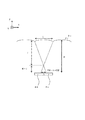
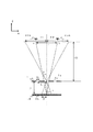
ここで、パララックスバリアが画像振分手段としての作用するための条件について詳述する。まず、図14を使用して、パララックスバリア方式について説明する。 Here, the conditions for the parallax barrier to function as the image distribution means will be described in detail. First, the parallax barrier method will be described with reference to FIG.
パララックスバリア7は、細い縦縞状の多数の開口、すなわち、スリット7aが形成されたバリア(遮光板)である。換言すれば、パララックスバリアは、振分方向となる第1の方向と直交する第2の方向に延びるスリットが、前記第1の方向に沿って複数本配列するように形成された光学部材である。左眼用画素4Lからパララックスバリア7に向けて出射した光は、スリット7aを透過すると、領域ELに向けて進行する光束となる。同様に、右眼用画素4Rからパララックスバリア7に向けて出射した光は、スリット7aを透過すると、領域ERに向けて進行する光束となる。このとき、観察者が左眼55Lを領域ELに位置させ、右眼55Rを領域ERに位置させた場合に、観察者は立体画像を認識することができる。
The
次に、表示パネルの前面にスリット状の開口部を有するパララックスバリアが配置された立体画像表示装置について、その各部のサイズを詳細に説明する。図14に示すように、パララックスバリア7のスリット7aの配列ピッチをLとし、パララックスバリア7と画素との距離をHとする。また、パララックスバリア7と観察者との間の距離を最適観察距離ODとする。更に、パララックスバリア7の中央に位置するスリット7aの中心から、X軸方向におけるパララックスバリア7の端に位置するスリット7aの中心までの距離をWLとする。パララックスバリア7自体は遮光板であるためスリット7a以外に入射した光は透過しないが、バリア層を支持する基板を設けることとし、この基板の屈折率をnと定義する。仮に支持基板が存在しない場合には、屈折率nを空気の屈折率である1にすればよい。このように定義すると、スリット7aから出射する光は、バリア層を支持する基板から出射する際に、スネルの法則に従って屈折する。そこで、パララックスバリア7の中央に位置するスリット7aにおける光の入射角及び出射角を夫々α及びβとし、X軸方向におけるパララックスバリア7の端に位置するスリット7aにおける光の入射角及び出射角を夫々γ及びδとする。更に、スリット7aの開口幅をS1とする。スリット7aの配列ピッチLと画素の配列ピッチPとは相互に関係しているため、一方に合わせて他方を決めることになるが、通常、表示パネルに合わせてパララックスバリアを設計することが多いため、画素の配列ピッチPを定数として扱う。また、バリア層の支持基板の材料を選択することにより、屈折率nが決定される。これに対して、パララックスバリアと観察者との間の観察距離OD、及び観察距離ODにおける画素拡大投影像の周期eは所望の値を設定する。これらの値を使用して、バリアと画素との間の距離H及びバリアピッチLを決定する。スネルの法則と幾何学的関係より、下記数式19乃至24が成立する。また、下記数式25乃至27が成立する。
Next, the size of each part of the stereoscopic image display device in which a parallax barrier having a slit-like opening is arranged on the front surface of the display panel will be described in detail. As shown in FIG. 14, the arrangement pitch of the
[数19]
n×sinα=sinβ
[Equation 19]
n × sin α = sin β
[数20]
OD×tanβ=e
[Equation 20]
OD × tan β = e
[数21]
H×tanα=P
[Equation 21]
H × tan α = P
[数22]
n×sinγ=sinδ
[Equation 22]
n × sin γ = sin δ
[数23]
H×tanγ=C
[Equation 23]
H × tan γ = C
[数24]
OD×tanδ=WL
[Equation 24]
OD × tan δ = WL
[数25]
WP−WL=C
[Equation 25]
WP-WL = C
[数26]
WP=2×m×P
[Equation 26]
WP = 2 × m × P
[数27]
WL=m×L
なお上記においては、左眼用画素と右眼用画素とを有する2視点の立体画像表示装置について説明したが、本発明はこれに限定されるものではない。例えば、N視点方式の表示装置に対して同様に適用することができる。この場合には、前述の距離WPの定義において、距離WPの領域に含まれる画素数を、2m個からN×m個に変更すればよい。
[Equation 27]
WL = m × L
In the above description, a two-viewpoint stereoscopic image display device having a left-eye pixel and a right-eye pixel has been described. However, the present invention is not limited to this. For example, the present invention can be similarly applied to an N-viewpoint display device. In this case, in the above-described definition of the distance WP, the number of pixels included in the area of the distance WP may be changed from 2m to N × m.
上記のパラメータについてまとめると、画素の配列ピッチPは表示パネルにより決定される値であり、観察距離OD及び画素拡大投影像の周期eは表示装置の設定により決定される値である。屈折率nは支持基板等の材質により決定される。そして、これらから導出されるスリットの配列ピッチL、パララックスバリアと画素との距離Hは、各画素からの光が観察面に投影される位置を決定するためのパラメータとなる。画像振分効果を変更するパラメータは、スリットの開口幅S1である。すなわち、バリアと画素との距離Hが固定の場合、スリットの開口幅S1が小さい程、左右の画素の像は明確に分離される。ピンホールカメラと同様の原理である。そして、開口幅S1が大きくなると、左右の画素の像がぼやけて、明確に分離しなくなる。 Summarizing the above parameters, the pixel arrangement pitch P is a value determined by the display panel, and the observation distance OD and the period e of the enlarged pixel projection image are values determined by the setting of the display device. The refractive index n is determined by the material of the support substrate or the like. The slit arrangement pitch L derived from these and the distance H between the parallax barrier and the pixels are parameters for determining the position at which the light from each pixel is projected onto the observation surface. The parameter for changing the image distribution effect is the opening width S1 of the slit. That is, when the distance H between the barrier and the pixel is fixed, the images of the left and right pixels are more clearly separated as the slit opening width S1 is smaller. The principle is the same as that of a pinhole camera. When the aperture width S1 is increased, the left and right pixel images are blurred and cannot be clearly separated.
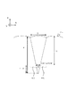
パララックスバリアにおいて分離が有効になるスリット幅の範囲は、レンズ方式よりも直感的に算出することができる。図15に示すように、左眼用画素4Lと右眼用画素4Rの境界から出射した光は、スリット7aを通過する際にその開口幅である幅S1に狭められる。そして、距離OD進行して観察面に到達するが、分離作用が存在するためには、この観察面における幅がe以下でなければならない。この幅より広がった場合には、左右画素の投影周期よりも大きくなるため、分離されないことになる。このときのスリット7aの開口幅S1は、スリットピッチLの半分である。すなわち、パララックスバリアにおいて分離が有効になるスリット幅の範囲は、スリットピッチの1/2以下である。
The range of the slit width in which separation is effective in the parallax barrier can be calculated more intuitively than in the lens system. As shown in FIG. 15, the light emitted from the boundary between the left-
本実施形態における上記以外の効果は、前述の第1実施形態と同様である。 The effects other than those described above in the present embodiment are the same as those in the first embodiment described above.
次に、本発明の第3実施形態について説明する。図16は本発明の第3実施形態に係る表示装置において、各画素の極性を示す上面図である。前述の本発明の第1実施形態と比較して、本第3実施形態においては、2ラインドット反転駆動を適用したことを特徴とする。2ラインドット反転駆動方法は、ドット反転駆動方法に対して、2ゲートライン毎に極性反転を実行する駆動方法である。2ラインドット反転駆動は1H2Vドット反転駆動とも称される。これは、水平方向(H方向)に配列するデータ線1本毎、また垂直方向(V方向)に配列するゲート線2本毎に極性が反転しているからである。 Next, a third embodiment of the present invention will be described. FIG. 16 is a top view showing the polarity of each pixel in the display device according to the third embodiment of the present invention. Compared to the first embodiment of the present invention described above, the third embodiment is characterized in that 2-line dot inversion driving is applied. The two-line dot inversion driving method is a driving method in which polarity inversion is performed every two gate lines with respect to the dot inversion driving method. Two-line dot inversion driving is also referred to as 1H2V dot inversion driving. This is because the polarity is inverted every one data line arranged in the horizontal direction (H direction) and every two gate lines arranged in the vertical direction (V direction).
すなわち、図16に示すように、ゲート線G1及びG2が選択された場合、データ線D1、D3、D5、D7には正極性の表示データが伝送され、データ線D2、D4、D6には負極性の表示データが伝送される。そして、ゲート線G3及びG4が選択された場合、データ線D1、D3、D5、D7には負極性の表示データが伝送され、データ線D2、D4、D6には正極性の表示データが伝送される。これにより、図16に示すような極性分布が実現される。ここで、右眼用画素4Rから構成される画素群に着目すると、2ライン反転効果が実現されていることが分かる。すなわち、Y軸方向には2個毎に異極性の画素が配置され、X軸方向には同極性の画素が配列している。左眼用画素4Lから構成される画素群も同様である。本実施形態における上記以外の構成は、前述の第1実施形態と同様である。
That is, as shown in FIG. 16, when the gate lines G1 and G2 are selected, the positive display data is transmitted to the data lines D1, D3, D5, and D7, and the negative lines are transmitted to the data lines D2, D4, and D6. Display data is transmitted. When the gate lines G3 and G4 are selected, negative display data is transmitted to the data lines D1, D3, D5, and D7, and positive display data is transmitted to the data lines D2, D4, and D6. The Thereby, the polarity distribution as shown in FIG. 16 is realized. Here, when attention is paid to the pixel group composed of the right-
本実施形態においては、各視点において2ライン反転効果を実現することができるだけでなく、画素の台形開口における底辺同士を同極性に配置することができる。これにより、底辺近傍における液晶分子の異常配向を抑制でき、高画質化が可能となる。また、下底間の遮光部の高さを低減することもでき、開口率を向上して明るい表示も実現できる。本第3実施形態における上記以外の効果は、前述の第1実施形態と同様である。 In the present embodiment, not only can the two-line inversion effect be realized at each viewpoint, but also the bases of the trapezoidal openings of the pixels can be arranged with the same polarity. Thereby, abnormal alignment of liquid crystal molecules in the vicinity of the bottom can be suppressed, and high image quality can be achieved. Further, the height of the light shielding portion between the lower bases can be reduced, and the aperture ratio can be improved to realize bright display. The other effects of the third embodiment are the same as those of the first embodiment.
次に、本発明の第4実施形態について説明する。図17は本発明の第4実施形態に係る表示装置において、各画素の極性を示す上面図である。前述の本発明の第3実施形態と比較して、本第4実施形態においては、ライン反転駆動を適用したことを特徴とする。ライン反転駆動方法は、1ライン毎に極性反転を実行する駆動方法であるが、データ線は同極性のみで構成される。そして、1ライン毎に対向電極の電位を変化させることで、データ線に伝送される表示データの極性を反転することなく、画素に書き込まれる表示データの極性を反転することができる。これにより、データ線駆動回路の耐圧を低減できるため、低コスト化が可能となる。 Next, a fourth embodiment of the present invention will be described. FIG. 17 is a top view showing the polarity of each pixel in the display device according to the fourth exemplary embodiment of the present invention. Compared to the third embodiment of the present invention described above, the fourth embodiment is characterized in that line inversion driving is applied. The line inversion driving method is a driving method in which polarity inversion is performed for each line, but the data lines are configured only with the same polarity. By changing the potential of the counter electrode for each line, the polarity of the display data written to the pixels can be reversed without inverting the polarity of the display data transmitted to the data line. As a result, the withstand voltage of the data line driving circuit can be reduced, so that the cost can be reduced.
図17に示すように、ゲート線G1、G3、G5の選択時には、データ線D1乃至D7に接続された画素には、正極性の表示データが書き込まれる。そして、ゲート線G2、G4の選択時には、データ線D1乃至D7に接続された画素には、負極性の表示データが書き込まれる。これにより、図17に示すような極性分布が実現される。ここで、右眼用画素4Rから構成される画素群に着目すると、全て正極性の画素から構成されていることがわかる。また、左眼用画素4Lから構成される画素群に着目すると、全て負極性の画素から構成されている。なお、次フレームにおいては極性反転が実行され、右眼用画素4Rから構成される画素群は全て負極性の画素から構成され、左眼用画素4Lから構成される画素群は全て正極性の画素から構成されることになる。本実施形態における上記以外の構成は、前述の第3実施形態と同様である。
As shown in FIG. 17, when the gate lines G1, G3, and G5 are selected, positive display data is written to the pixels connected to the data lines D1 to D7. When the gate lines G2 and G4 are selected, negative display data is written to the pixels connected to the data lines D1 to D7. Thereby, a polarity distribution as shown in FIG. 17 is realized. Here, when attention is paid to the pixel group composed of the right-
本実施形態においては、各視点においてフレーム反転効果を実現することができる。また、画素の台形開口における底辺同士を同極性に配置することもでき、高画質化が可能となる。本第4実施形態における上記以外の効果は、前述の第3実施形態と同様である。 In the present embodiment, a frame inversion effect can be realized at each viewpoint. In addition, the bases of the trapezoidal openings of the pixels can be arranged with the same polarity, so that high image quality can be achieved. The other effects of the fourth embodiment are the same as those of the third embodiment.
次に、本発明の第5実施形態について説明する。図18は本発明の第5実施形態に係る表示装置において、各画素の極性を示す上面図である。前述の本発明の第4実施形態と比較して、本第5実施形態においては、2ライン反転駆動を適用したことを特徴とする。 Next, a fifth embodiment of the present invention will be described. FIG. 18 is a top view showing the polarity of each pixel in the display device according to the fifth exemplary embodiment of the present invention. Compared to the above-described fourth embodiment of the present invention, the fifth embodiment is characterized in that 2-line inversion driving is applied.
すなわち、図18に示すように、ゲート線G1、G2、G5の選択時には、データ線D1乃至D7に接続された画素には正極性の表示データが書き込まれ、ゲート線G2、G4の選択時には、データ線D1乃至D7に接続された画素には負極性の表示データが書き込まれる。なお、次フレームにおいては、正負の極性は反転される。ここで、右眼用画素4Rから構成される画素群に着目すると、図示したフレームにおいては、正負両極性の画素が2ライン反転の状態で配置されることになる左眼用画素4Lから構成される画素群も同様である。本実施形態における上記以外の構成は、前述の第4実施形態と同様である。
That is, as shown in FIG. 18, when the gate lines G1, G2, and G5 are selected, positive display data is written to the pixels connected to the data lines D1 to D7, and when the gate lines G2 and G4 are selected, Negative display data is written to the pixels connected to the data lines D1 to D7. In the next frame, the positive and negative polarities are inverted. Here, focusing on the pixel group composed of the right-
本実施形態においては、2ライン反転駆動を適用することにより、ライン反転駆動を基本としても、2ライン反転ではあるが、ライン反転効果を発揮することが可能となる。これにより、各視点の極性分布をライン状に微細化でき、フレーム反転効果のみの場合よりも高画質化が可能となる。本第5実施形態における上記以外の効果は、前述の第4実施形態と同様である。 In the present embodiment, by applying the 2-line inversion drive, the line inversion effect can be exhibited even though the line inversion drive is basically used, although it is the 2-line inversion. Thereby, the polarity distribution at each viewpoint can be made finer in a line shape, and higher image quality can be achieved than in the case of only the frame inversion effect. The other effects of the fifth embodiment are the same as those of the fourth embodiment.
次に、本発明の第6実施形態について説明する。図19は本発明の第6実施形態に係る表示装置において、各画素の極性を示す上面図である。前述の本発明の第4実施形態と比較して、本第6実施形態においては、フレーム反転駆動を適用したことを特徴とする。フレーム反転駆動は、フレーム間はデータ線の極性を反転させない方法である。すなわち、走査線が一巡する間は、全面で一定の極性を与え、次の走査線の周期で極性を反転する方法である。 Next, a sixth embodiment of the present invention will be described. FIG. 19 is a top view showing the polarity of each pixel in the display device according to the sixth exemplary embodiment of the present invention. Compared to the fourth embodiment of the present invention described above, the sixth embodiment is characterized in that frame inversion driving is applied. The frame inversion driving is a method in which the polarity of the data line is not inverted between frames. That is, while the scanning line goes around, a constant polarity is given to the entire surface, and the polarity is inverted at the period of the next scanning line.
すなわち、図19に示すように、ゲート線G1乃至G5の選択時には、データ線D1乃至D7に接続された画素には正極性の表示データが書き込まれる。そして次のフレームにおいては、負極性の表示データが書き込まれる。この結果、各フレームにおいて、右眼用画素4Rから構成される画素群も、左眼用画素4Lから構成される画素群も、全て同極性となる。本実施形態における上記以外の構成は、前述の第4実施形態と同様である。
That is, as shown in FIG. 19, when the gate lines G1 to G5 are selected, positive display data is written to the pixels connected to the data lines D1 to D7. In the next frame, negative display data is written. As a result, in each frame, the pixel group composed of the
本実施形態においては、フレーム反転駆動を適用することにより、各視点の極性を同様に揃えることができる。更には、画素の台形開口における底辺同士を同極性に配置できるだけでなく、斜辺同士も同極性にできるため、液晶分子の異常配向を抑制でき、高画質化が可能となる。 In the present embodiment, by applying the frame inversion drive, the polarities of the respective viewpoints can be similarly aligned. Furthermore, not only can the bases of the trapezoidal openings of the pixels be arranged with the same polarity, but also the hypotenuses can be made with the same polarity, so that abnormal alignment of liquid crystal molecules can be suppressed and high image quality can be achieved.
なお、本実施形態においては、ライン反転効果やドット反転効果など空間的に極性を分布させることで均一化する効果は望めない。そこで、特に倍速化などフレーム周波数を大きくすることにより、時間軸上で均一化して、表示品質を向上することができる。このために有効なフレーム周波数は、70Hz以上である。本第6実施形態における上記以外の効果は、前述の第4実施形態と同様である。 In the present embodiment, it is not possible to expect the effect of uniforming the spatial distribution of polarity such as the line inversion effect and the dot inversion effect. In view of this, it is possible to improve the display quality by making the frame frequency uniform, such as double speed, and making it uniform on the time axis. For this purpose, an effective frame frequency is 70 Hz or more. The other effects of the sixth embodiment are the same as those of the fourth embodiment described above.
次に、本発明の第7実施形態について説明する。図20は本発明の第7実施形態に係る表示装置において、各画素の極性を示す上面図である。前述の本発明の第1実施形態と比較して、本第7実施形態においては、2H1V反転駆動を適用したことを特徴とする。2H1V反転法とは、データ線は2本単位で極性が反転され、ゲート線は1本毎に極性が反転される駆動方法である。 Next, a seventh embodiment of the present invention will be described. FIG. 20 is a top view showing the polarity of each pixel in the display device according to the seventh exemplary embodiment of the present invention. Compared to the first embodiment of the present invention described above, the seventh embodiment is characterized in that 2H1V inversion driving is applied. The 2H1V inversion method is a driving method in which the polarity of data lines is inverted in units of two and the polarity of each gate line is inverted.
すなわち、図20に示すように、ゲート線G1の選択時には、データ線D1、D2、D5、D6に接続された画素には正極性の表示データが書き込まれ、データ線D3、D4、D7に接続された画素には負極性の表示データが書き込まれる。次に、ゲート線G2の選択時には、データ線D1、D2、D5、D6に接続された画素には負極性の表示データが書き込まれ、データ線D3、D4、D7に接続された画素には正極性の表示データが書き込まれる。なお、次フレームにおいては、上記の極性を反転した表示データが書き込まれる。この結果、右眼用画素4Rから構成される画素群においては、同極性の画素が縦方向に配列し、異極性の画素が横方向に配列したカラム反転効果が得られる。一方で、左眼用画素4Lから構成される画素群においては、ドット反転効果が得られる。
That is, as shown in FIG. 20, when the gate line G1 is selected, positive display data is written to the pixels connected to the data lines D1, D2, D5, and D6, and connected to the data lines D3, D4, and D7. Negative display data is written in the pixel thus formed. Next, when the gate line G2 is selected, negative display data is written to the pixels connected to the data lines D1, D2, D5, and D6, and the positive electrodes are connected to the pixels connected to the data lines D3, D4, and D7. Display data is written. In the next frame, display data with the polarity reversed is written. As a result, in the pixel group composed of the right-
ここで、蓄積容量線について着目する。特に、ゲート線G1とG2の間に配置された蓄積容量線は、画素P11、P23、P13、P25、P27、P17に接続されることになる。そして、ゲート線G1が選択された時には、画素P11、P13、P17に表示データの書込動作が実行されるが、2H1V反転駆動を適用した場合には、P11には正極性、P13には負極性、P17には正極性の表示データが書き込まれることになる。このように、各蓄積容量線に接続されゲート線選択時に書き込みされる複数の画素は、正極性の表示データが書き込まれる画素と負極性のデータが書き込まれる画素とから構成されている。本実施形態における上記以外の構成は、前述の第1実施形態と同様である。 Here, attention is paid to the storage capacitor line. In particular, the storage capacitor line disposed between the gate lines G1 and G2 is connected to the pixels P11, P23, P13, P25, P27, and P17. When the gate line G1 is selected, display data is written to the pixels P11, P13, and P17. When 2H1V inversion driving is applied, P11 has a positive polarity and P13 has a negative polarity. The display data of positive polarity is written in P17. In this way, the plurality of pixels connected to each storage capacitor line and written when the gate line is selected are composed of pixels to which positive display data is written and pixels to which negative data is written. Other configurations in the present embodiment are the same as those in the first embodiment.
本実施形態においては、左右の画素群で反転効果が異なるものの、少なくとも一方の視点においてはドット反転効果を実現することができる。これにより、少なくとも一視点においては、高画質化が可能となる。一般的に人間は、左右両眼の視認状態が異なる場合、より視認状態に優れた方の情報を活用することができる。例えば、両眼の視力が異なる場合には、より視力の優れた方の眼の映像が認識され、特に細部が補足されている。本実施形態においては、左眼の視認するドット反転効果の表示が、右眼の視認するカラム反転効果の表示よりも優れていると、左眼の優れた表示を利用して、視認する表示品質を向上することができる。このように、両眼用の表示品質が共に低いよりは、片方のみでも表示品質を向上することにより、全体の品質向上が可能となる。 In this embodiment, although the inversion effect differs between the left and right pixel groups, the dot inversion effect can be realized at least at one viewpoint. This makes it possible to improve the image quality at least from one viewpoint. In general, when the viewing states of the left and right eyes are different, a person can use information with a better viewing state. For example, when the visual acuity of both eyes is different, the image of the eye with the better visual acuity is recognized, and details are particularly supplemented. In this embodiment, when the display of the dot reversal effect visually recognized by the left eye is superior to the display of the column reversal effect visually recognized by the right eye, the display quality visually recognized using the excellent display of the left eye Can be improved. As described above, it is possible to improve the overall quality by improving the display quality of only one of the two, rather than the display quality for both eyes being low.
更に、本実施形態においては、各画素への表示データの書き込み時に、蓄積容量線の電位変動を抑制することができる。これは、各蓄積容量線には、正極性の表示データが書き込みされる画素だけでなく、負極性の表示データが書き込まれる画素が接続されているからである。これにより、蓄積容量線の電位が片側の極性に向かって変動するのを抑制することができ、横方向のクロストークなどを低減して、高品質な表示を実現することができる。本第7実施形態における上記以外の効果は、前述の第1実施形態と同様である。 Furthermore, in the present embodiment, the potential fluctuation of the storage capacitor line can be suppressed when display data is written to each pixel. This is because each storage capacitor line is connected not only to pixels to which positive display data is written, but also to pixels to which negative display data is written. Thereby, it is possible to suppress the potential of the storage capacitor line from fluctuating toward the polarity on one side, and it is possible to reduce the crosstalk in the horizontal direction and realize high-quality display. The other effects of the seventh embodiment are the same as those of the first embodiment.
次に、本発明の第8実施形態について説明する。図21は本発明の第8実施形態に係る表示装置において、各画素の極性を示す上面図である。前述の本発明の第7実施形態と比較して、本第8実施形態においては、2H2V反転駆動を適用したことを特徴とする。2H2V反転法とは、データ線は2本単位で極性が反転され、ゲート線も2本単位で極性が反転される駆動方法である。 Next, an eighth embodiment of the present invention will be described. FIG. 21 is a top view showing the polarity of each pixel in the display device according to the eighth embodiment of the present invention. Compared to the seventh embodiment of the present invention described above, the eighth embodiment is characterized in that 2H2V inversion driving is applied. The 2H2V inversion method is a driving method in which the polarity of data lines is inverted in units of two and the polarity of gate lines is also inverted in units of two.
すなわち、図21に示すように、ゲート線G1の選択時には、データ線D1、D2、D5、D6に接続された画素には正極性の表示データが書き込まれ、データ線D3、D4、D7に接続された画素には負極性の表示データが書き込まれる。次に、ゲート線G2の選択時にも同様である。そして、ゲート線G3の選択時には、データ線D1、D2、D5、D6に接続された画素には負極性の表示データが書き込まれ、データ線D3、D4、D7に接続された画素には正極性の表示データが書き込まれる。次のゲート線G4の選択時も同様である。なお、次フレームにおいては、上記の極性を反転した表示データが書き込まれる。この結果、右眼用画素4Rから構成される画素群は、2ラインドット反転(1H2Vドット反転)効果が得られる極性分布となっている。そして、左眼用画素4Lから構成される画素群も同様である。本実施形態における上記以外の構成は、前述の第1実施形態と同様である。
That is, as shown in FIG. 21, when the gate line G1 is selected, positive display data is written to the pixels connected to the data lines D1, D2, D5, and D6 and connected to the data lines D3, D4, and D7. Negative display data is written in the pixel thus formed. The same applies to the selection of the gate line G2. When the gate line G3 is selected, negative display data is written to the pixels connected to the data lines D1, D2, D5, and D6, and the positive polarity is applied to the pixels connected to the data lines D3, D4, and D7. Display data is written. The same applies when the next gate line G4 is selected. In the next frame, display data with the polarity reversed is written. As a result, the pixel group composed of the right-
本実施形態においては、各視点用画素の画素群が同様に2ラインドット反転効果を得ることができるため、表示品質の向上が可能となる。また、前述の第7実施形態と同様に、各蓄積容量線の変動も抑制することができる。 In the present embodiment, since the pixel group of each viewpoint pixel can similarly obtain the 2-line dot inversion effect, display quality can be improved. Further, similarly to the above-described seventh embodiment, the fluctuation of each storage capacitor line can also be suppressed.
前述の第3実施形態や第5実施形態にも記載のように、本発明の画素構造においては、ゲート線2本毎に極性反転する2V反転駆動を好適に組み合わせることができる。本第8実施形態における上記以外の効果は、前述の第1実施形態と同様である。 As described in the third embodiment and the fifth embodiment described above, in the pixel structure of the present invention, 2V inversion driving for polarity inversion every two gate lines can be suitably combined. The other effects of the eighth embodiment are the same as those of the first embodiment.
次に、本発明の第9実施形態について説明する。図22は本発明の第9実施形態に係る表示装置において、各画素の極性を示す上面図であり、図23は本実施形態に係る表示装置において各ゲート線選択時のデータ線極性を示す表である。前述の本発明の第1実施形態と比較して、本第9実施形態においては、2H1V反転駆動を基本とし、更に同極性のブロックをずらしていく駆動方法を適用したことを特徴とする。 Next, a ninth embodiment of the present invention will be described. FIG. 22 is a top view showing the polarity of each pixel in the display device according to the ninth embodiment of the present invention, and FIG. 23 is a table showing the data line polarity when each gate line is selected in the display device according to this embodiment. It is. Compared to the first embodiment of the present invention described above, the ninth embodiment is characterized in that the driving method is based on 2H1V inversion driving and the blocks having the same polarity are shifted.
すなわち、図22及び図23に示すように、ゲート線G1の選択時には、データ線D1乃至D4に接続された画素には夫々正、負、負、正極性の表示データが書き込まれる。なお、データ線方向に対しては、このセットが繰り返される。すなわち、データ線D5乃至D7に接続された画素には、夫々正、負、負極性の表示データが書き込まれる。以降、データ線D1乃至D4に着目すると、ゲート線G2の選択時には正、正、負、負であり、ゲート線G3の選択時には負、正、正、負であり、ゲート線G4の選択時には負、負、正、正となる。ゲート線G5以降に関しては、ゲート線G1乃至G4が繰り返される。すなわち、図23の太枠で示した極性分布を基本とし、X軸方向Y軸方向に繰り返し配置したものとなる。このように、本実施形態においては、データ線は2本単位で極性が反転され、ゲート線は1本毎に極性が反転される2H1V反転駆動を基本としているが、ゲート線毎にデータ線1本分だけ極性分布がずれていく点が2H1V反転駆動とは異なる。換言すれば、奇数番目の前記ゲート線選択時と偶数番目の前記ゲート線選択時とで、前記データ線に伝送される表示データの極性が前記データ線1本分だけ異なっている。
That is, as shown in FIGS. 22 and 23, when the gate line G1 is selected, display data of positive, negative, negative, and positive polarity is written to the pixels connected to the data lines D1 to D4, respectively. This set is repeated for the data line direction. That is, positive, negative, and negative display data is written to the pixels connected to the data lines D5 to D7, respectively. Subsequently, focusing on the data lines D1 to D4, they are positive, positive, negative, and negative when the gate line G2 is selected, negative, positive, positive, and negative when the gate line G3 is selected, and negative when the gate line G4 is selected. , Negative, positive, positive. With respect to the gate line G5 and thereafter, the gate lines G1 to G4 are repeated. That is, it is based on the polarity distribution shown by the thick frame in FIG. 23 and is repeatedly arranged in the X-axis direction and the Y-axis direction. As described above, in the present embodiment, the polarity of the data line is inverted in units of two and the gate line is based on the 2H1V inversion driving in which the polarity is inverted for each line. However, the
この結果、右眼用画素4Rから構成される画素群は、2ラインドット反転(1H2Vドット反転)効果が得られる極性分布となっている。そして、左眼用画素4Lから構成される画素群も同様である。本実施形態における上記以外の構成は、前述の第1実施形態と同様である。
本実施形態においては、各視点の極性分布を同様に2ラインドット反転とすることができる。更に、各蓄積容量線の電位変動も抑制でき、台形開口の底辺部が隣接する画素の極性を同じにできる。これにより、表示品質の向上が可能となる。
As a result, the pixel group composed of the right-
In the present embodiment, the polarity distribution at each viewpoint can be similarly set to 2-line dot inversion. Furthermore, the potential fluctuation of each storage capacitor line can be suppressed, and the polarities of the pixels adjacent to the bottom of the trapezoidal opening can be made the same. Thereby, display quality can be improved.
なお、本実施形態においては、特にゲート線を1本おきに走査する駆動方法を好適に適用することができる。すなわち、奇数番目のゲート線を順次選択した際には、単なる2H1V反転駆動を適用すればよい。そして、偶数番目のゲート線を順次選択した際には、同極性のブロックを1列分だけずらした状態で、2H1V反転駆動を適用すればよい。通常の2H1V反転駆動が可能なドライバICでは、このように同極性のブロックを制御できるオプションが準備されているため、通常の2H1V反転駆動を容易に流用することができる。なお、奇数番目のゲート線走査と偶数番目のゲート線走査は、フレーム期間内で終了することが好ましい。すなわち、単なるインタレース駆動ではなく、倍速インタレース駆動が好ましい。 In the present embodiment, a driving method of scanning every other gate line can be suitably applied. That is, when odd-numbered gate lines are sequentially selected, simple 2H1V inversion driving may be applied. Then, when the even-numbered gate lines are sequentially selected, the 2H1V inversion drive may be applied in a state where the blocks having the same polarity are shifted by one column. In a driver IC capable of normal 2H1V inversion driving, an option capable of controlling blocks having the same polarity is prepared in this way, and therefore normal 2H1V inversion driving can be easily used. Note that the odd-numbered gate line scan and the even-numbered gate line scan are preferably finished within the frame period. That is, double-speed interlace driving is preferable rather than simple interlace driving.
また、ゲート線を駆動するゲート線駆動回路に関しては、奇数番目のゲート線と偶数番目のゲート線とが異なるゲート線駆動回路に接続されていてもよい。これにより、ゲート線を1本おきに走査するのが容易になる。 As for the gate line driving circuit for driving the gate lines, the odd-numbered gate lines and the even-numbered gate lines may be connected to different gate line driving circuits. This facilitates scanning every other gate line.
更にまた、本実施形態における表示画像の入力フォーマットは、左右画像を上下方向に配置した形式や、左右画像を時系列で配置した形式を好適に適用することができる。前述のように、奇数番目のゲート線のみを順次選択すると、右眼用の画像を表示する画素にのみ書込を実行することができる。次に偶数番目のゲート線のみを順次選択すると、左眼用の画像を表示する画素にのみ書込を実行することができる。このように、同一視点の画像情報が連続して入力されるフォーマットに対して、同一視点用の画素にのみ書込を実行することのできる駆動方法を好適に適用でき、駆動回路を簡素化することができる。本第9実施形態における上記以外の効果は、前述の第1実施形態と同様である。 Furthermore, as the display image input format in this embodiment, a format in which left and right images are arranged in the vertical direction and a format in which left and right images are arranged in time series can be suitably applied. As described above, when only the odd-numbered gate lines are sequentially selected, writing can be executed only to the pixels displaying the right-eye image. Next, when only even-numbered gate lines are sequentially selected, writing can be executed only to the pixels that display the image for the left eye. As described above, a driving method capable of executing writing only to pixels for the same viewpoint can be suitably applied to a format in which image information of the same viewpoint is continuously input, and the driving circuit is simplified. be able to. The other effects of the ninth embodiment are the same as those of the first embodiment.
次に、本発明の第10実施形態について説明する。図24は本発明の第10実施形態に係る表示装置において、各画素の極性を示す上面図である。前述の本発明の第1実施形態と比較して、本第10実施形態においては、線対称の関係に配置した隣接画素対を有することを特徴とする。 Next, a tenth embodiment of the present invention will be described. FIG. 24 is a top view showing the polarity of each pixel in the display device according to the tenth embodiment of the present invention. Compared to the first embodiment of the present invention described above, the tenth embodiment is characterized by having adjacent pixel pairs arranged in a line symmetrical relationship.
すなわち、図24に示すように、画素P22及び画素23から構成される隣接画素対においては、共通のゲート線G2より−Y方向に位置する画素P22は−X方向に位置するデータ線D2に接続され、ゲート線G2より+Y方向に位置する画素P23は+X方向に位置するデータ線D3に接続される。すなわち、この隣接画素対は、各画素が共通のゲート線を挟み上下に配置されるとき、上側の画素が右側のデータ線に接続されていることになる。 That is, as shown in FIG. 24, in the adjacent pixel pair composed of the pixel P22 and the pixel 23, the pixel P22 located in the −Y direction from the common gate line G2 is connected to the data line D2 located in the −X direction. Then, the pixel P23 located in the + Y direction from the gate line G2 is connected to the data line D3 located in the + X direction. That is, in the adjacent pixel pair, when the pixels are arranged above and below the common gate line, the upper pixel is connected to the right data line.
一方で、画素P31及び画素P32から構成される隣接画素対においては、共通のゲート線G3より−Y方向に位置する画素P32は+X方向に位置するデータ線D2に接続され、ゲート線G3より+Y方向に位置する画素P31は−X方向に位置するデータ線D1に接続される。すなわち、この隣接画素対は、各画素が共通のゲート線を挟み上下に配置されるとき、上側の画素が左側のデータ線に接続されていることになる。図24においては、このように、上側の画素が左側のデータ線に接続される隣接画素対を、点線で示す丸で囲って示している。そして、上側の画素が左側のデータ線に接続される隣接画素対は、+X方向に隣接する画素列においては、−Y方向に隣接するゲート線に対して配置されている。この結果、同種の隣接画素対は斜め方向に配置されていることになる。また、見方を変えれば、本実施形態においては、上側の画素が左側のデータ線に接続された隣接画素対と、上側の画素が右側のデータ線に接続された隣接画素対とが配置されていると表現することもできる。更にまた、この2種類の隣接画素対は、Y軸方向に延伸する線分に対して線対称の関係でもあるし、X軸方向に延伸する線分に関しても線対称の関係となっている。すなわち、ゲート線の延伸方向又はその直交方向に対して、線対称の配置関係にあると言える。 On the other hand, in the adjacent pixel pair composed of the pixel P31 and the pixel P32, the pixel P32 located in the −Y direction from the common gate line G3 is connected to the data line D2 located in the + X direction, and + Y from the gate line G3. The pixel P31 located in the direction is connected to the data line D1 located in the −X direction. That is, in the adjacent pixel pair, when the pixels are arranged above and below the common gate line, the upper pixel is connected to the left data line. In FIG. 24, adjacent pixel pairs in which the upper pixel is connected to the left data line are surrounded by a circle indicated by a dotted line. The adjacent pixel pair in which the upper pixel is connected to the left data line is arranged with respect to the gate line adjacent in the −Y direction in the pixel column adjacent in the + X direction. As a result, the same type of adjacent pixel pair is arranged in an oblique direction. In other words, in this embodiment, an adjacent pixel pair in which the upper pixel is connected to the left data line and an adjacent pixel pair in which the upper pixel is connected to the right data line are arranged. It can also be expressed as being. Furthermore, these two types of adjacent pixel pairs have a line-symmetric relationship with respect to a line segment extending in the Y-axis direction, and also have a line-symmetric relationship with respect to a line segment extending in the X-axis direction. That is, it can be said that it is in a line-symmetric arrangement relationship with respect to the extending direction of the gate line or the direction perpendicular thereto.
そして、駆動方法に関しては、前述の第1実施形態と同様にドット反転駆動が実行されている。この結果、右眼用画素4Rから構成される画素群は、2ラインドット反転(1H2Vドット反転)効果が得られる極性分布となっている。そして、左眼用画素4Lから構成される画素群も同様である。なお、本実施形態における極性分布の基本セットは、X軸方向4画素、Y軸方向4画素の合計16画素であり、図24においては破線で囲って示している。本実施形態における上記以外の構成は、前述の第1実施形態と同様である。
本実施形態においては、一般的なドット反転駆動を使用した上で、前述の第9実施形態と同様に、2ラインドット反転効果、各蓄積容量線の電位変動抑制効果を実現でき、かつ台形開口の底辺部が隣接する画素の極性を同じにできる。これにより、低コストに高画質表示を実現することができる。
As for the driving method, the dot inversion driving is executed as in the first embodiment. As a result, the pixel group composed of the right-
In this embodiment, after using a general dot inversion drive, the two-line dot inversion effect and the potential fluctuation suppressing effect of each storage capacitor line can be realized, and the trapezoidal aperture can be realized as in the ninth embodiment. The polarities of pixels adjacent to each other at the bottom can be the same. Thereby, high-quality display can be realized at low cost.
なお、2種類の隣接画素対の配置は、本実施形態の説明に限定されるものではない。異種の隣接画素対を複数行毎、複数列毎に配置することもできる。特に、異なる隣接画素対を配置することによって、液晶分子の異常配向などが発生した場合でも、その影響を低減することができる。これは、画素構造が異なると異常配向などが発生する位置も異なるため、全画素で同様の位置に異常が発生するのを防止できるからである。特に本発明の複数視点表示装置においては、レンズなどの画像分離手段を用いて画素を拡大するので、本効果は非常に大きい。本第10実施形態における上記以外の効果は、前述の第1実施形態と同様である。 The arrangement of two types of adjacent pixel pairs is not limited to the description of the present embodiment. Different types of adjacent pixel pairs can be arranged for each of a plurality of rows and a plurality of columns. In particular, by arranging different adjacent pixel pairs, even when abnormal alignment of liquid crystal molecules occurs, the influence can be reduced. This is because, if the pixel structure is different, the position at which abnormal orientation or the like is generated is different, so that it is possible to prevent an abnormality from occurring at the same position in all pixels. In particular, in the multi-viewpoint display device of the present invention, since the pixels are enlarged using image separation means such as a lens, this effect is very great. The other effects of the tenth embodiment are the same as those of the first embodiment.
次に、本発明の第11実施形態について説明する。図25は本発明の第11実施形態に係る表示装置において、各画素の極性を示す上面図である。前述の本発明の第10実施形態と比較して、本第11実施形態においては、カラム反転駆動を適用したことを特徴とする。カラム反転駆動は、データ線毎に異なる極性の表示データが伝送され、ゲート線毎には反転動作が実行されない駆動方法である。 Next, an eleventh embodiment of the present invention will be described. FIG. 25 is a top view showing the polarity of each pixel in the display device according to the eleventh embodiment of the present invention. Compared to the tenth embodiment of the present invention described above, the eleventh embodiment is characterized by applying column inversion driving. The column inversion driving is a driving method in which display data having a different polarity is transmitted for each data line, and the inversion operation is not performed for each gate line.
図25に示すように、ゲート線G1選択時においては、データ線D1、D3、D5、D7に接続された画素には正極性の表示データが書き込まれ、データ線D2、D4、D6に接続された画素には負極性の表示データが書き込まれる。ゲート線G2乃至G5の選択時においても同様である。なお、次フレームにおいては、上記の極性を反転した表示データが書き込まれる。この結果、右眼用画素4Rから構成される画素群は、2ラインドット反転(1H2Vドット反転)効果が得られる極性分布となっている。そして、左眼用画素4Lから構成される画素群も同様である。本実施形態における上記以外の構成は、前述の第10実施形態と同様である。
As shown in FIG. 25, when the gate line G1 is selected, positive display data is written to the pixels connected to the data lines D1, D3, D5, and D7 and connected to the data lines D2, D4, and D6. The negative display data is written to the pixels. The same applies to the selection of the gate lines G2 to G5. In the next frame, display data with the polarity reversed is written. As a result, the pixel group composed of the right-
本実施形態においては、カラム反転駆動を適用した上で、前述の第10実施形態と同様の効果を発揮することができる。なお、カラム反転駆動は、ドット反転駆動において、ゲート線を順次操作走査する差異の極性反転をしない駆動方法である。すなわち、ドット反転駆動が可能なドライバICは、必ずカラム反転駆動も可能である。そして、ゲート線を順次走査する差異の極性反転がないので、カラム反転駆動はドット反転駆動よりも低電力化が可能になる。一般的な画素構造では、カラム反転駆動を採用すると、極性分布が一次元状となってしまい、表示画質がドット反転駆動より低下してしまう。しかし、本実施形態の画素構造によれば、カラム反転駆動を適用しても2ラインドット反転効果を発揮することができるため、低電力化と高画質化を両立することができる。本第11実施形態における上記以外の効果は、前述の第10実施形態と同様である。 In the present embodiment, the same effects as those of the tenth embodiment described above can be exhibited after applying column inversion driving. Note that the column inversion driving is a driving method in which the polarity inversion of the difference of sequentially scanning the gate lines is not performed in the dot inversion driving. That is, a driver IC capable of dot inversion driving can always perform column inversion driving. Since there is no polarity reversal of the difference of sequentially scanning the gate lines, the column reversal drive can achieve lower power than the dot reversal drive. In a general pixel structure, when column inversion driving is employed, the polarity distribution becomes one-dimensional, and the display image quality is lower than that of dot inversion driving. However, according to the pixel structure of the present embodiment, the two-line dot inversion effect can be exhibited even when column inversion driving is applied, so that both low power and high image quality can be achieved. The other effects of the eleventh embodiment are the same as those of the tenth embodiment.
次に、本発明の第12実施形態について説明する。図26は本発明の第12実施形態に係る表示装置において、画素を示す上面図である。前述の本発明の第1実施形態と比較して、本第12実施形態においては、積層配置されたデータ線又は蓄積容量線の一部に、容量カップリングを低減するための構造を設けたことを特徴とする。 Next, a twelfth embodiment of the present invention will be described. FIG. 26 is a top view showing pixels in a display device according to the twelfth embodiment of the present invention. Compared to the first embodiment of the present invention described above, in the twelfth embodiment, a structure for reducing the capacitive coupling is provided in a part of the stacked data lines or storage capacitor lines. It is characterized by.
図26に示すように、データ線Dと積層配置された蓄積容量線CSの一部には、配線が形成されていない刳り貫き状の穴が形成されている。本実施形態における上記以外の構成は、前述の第1実施形態と同様である。 As shown in FIG. 26, a part of the storage capacitor line CS that is laminated with the data line D is formed with a hollow hole in which no wiring is formed. Other configurations in the present embodiment are the same as those in the first embodiment.
本実施形態においては、データ線と蓄積容量線の電気的なカップリングを低減することができ、高画質化が可能となる。特に、開口率に与える影響が大きな斜行配線部分に対して、本実施形態を適用することにより、開口率を高めることもできる。 In this embodiment, the electrical coupling between the data line and the storage capacitor line can be reduced, and the image quality can be improved. In particular, the aperture ratio can be increased by applying this embodiment to the oblique wiring portion having a large influence on the aperture ratio.
なお、容量カップリングの低減構造は、前述の形状に限定されるものではない。例えば、一方の配線に多数の穴が形成されていてもよいし、配線の一部が抉れたような形状になっていてもよい。更には、蓄積容量線ではなくデータ線に対して、上述の構造が適用されていてもよい。なお、本構造を適用するにあたっては、データ線と蓄積容量線との間に隙間が発生しないように構成するのが望ましい。隙間が発生すると光漏れの原因となり、TFT基板と対向基板との位置合わせがずれた場合などに、表示画質の低下を招くからである。本第12実施形態における上記以外の効果は、前述の第1実施形態と同様である。 Note that the structure for reducing capacitive coupling is not limited to the shape described above. For example, a large number of holes may be formed in one wiring, or a shape in which a part of the wiring is curled may be formed. Furthermore, the above-described structure may be applied to the data line instead of the storage capacitor line. When applying this structure, it is desirable to configure so that no gap is generated between the data line and the storage capacitor line. This is because when the gap is generated, light leakage is caused, and the display image quality is deteriorated when the alignment between the TFT substrate and the counter substrate is shifted. The other effects of the twelfth embodiment are the same as those of the first embodiment.
次に、本発明の第13実施形態について説明する。図27は本発明の第13実施形態に係る表示装置において、画素を示す上面図である。前述の本発明の第1実施形態と比較して、本第13実施形態においては、薄膜トランジスタがダブルゲート構造である点を特徴とする。 Next, a thirteenth embodiment of the present invention is described. FIG. 27 is a top view showing pixels in a display device according to the thirteenth embodiment of the present invention. Compared to the first embodiment of the present invention, the thirteenth embodiment is characterized in that the thin film transistor has a double gate structure.
図27に示すように、薄膜トランジスタ4TFTのソース電極とドレイン電極は、ゲート線Gを跨いで配置されている。これは、ダブルゲート構造の各薄膜トランジスタに共通している。そして、一方の薄膜トランジスタのソース電極と、もう一方の薄膜トランジスタのドレイン電極が接続されている。この結果、ダブルゲート構造はW方向をゲート線延伸方向と一致させたU字型となっている。本実施形態における上記以外の構成は、前述の第1実施形態と同様である。 As shown in FIG. 27, the source electrode and the drain electrode of the thin film transistor 4TFT are disposed across the gate line G. This is common to each thin film transistor having a double gate structure. The source electrode of one thin film transistor and the drain electrode of the other thin film transistor are connected. As a result, the double gate structure has a U shape in which the W direction coincides with the gate line extending direction. Other configurations in the present embodiment are the same as those in the first embodiment.
本実施形態においては、特に薄膜トランジスタの半導体層に対して、移動度が大きな低温ポリシリコンや単結晶シリコンを適用した場合に、トランジスタオフ時のリーク電力を低減することができる。これにより、高画質な表示が可能となる。また、ダブルゲート構造においても、トランジスタのW方向をゲート線の延伸方向と一致させ、かつソース電極とドレイン電極をゲート線を跨いで配置することにより、開口率の低下を抑制することができ、高画質表示が可能となる。なお、トリプルゲート構造などの他の複数ゲート構造においても、本実施形態を同様に適用することができる。本第13実施形態における上記以外の効果は、前述の第1実施形態と同様である。 In this embodiment, particularly when low temperature polysilicon or single crystal silicon having high mobility is applied to the semiconductor layer of the thin film transistor, the leakage power when the transistor is off can be reduced. Thereby, high-quality display is possible. Also in the double gate structure, by reducing the aperture ratio by aligning the W direction of the transistor with the extending direction of the gate line and disposing the source electrode and the drain electrode across the gate line, High-quality display is possible. Note that the present embodiment can be similarly applied to other multiple gate structures such as a triple gate structure. The other effects of the thirteenth embodiment are the same as those of the first embodiment.
次に、本発明の第14実施形態について説明する。図28は本発明の第14実施形態に係る表示装置において、画素を示す上面図である。前述の本発明の第1実施形態と比較して、本第14実施形態においては、薄膜トランジスタのサイズと配置が異なる。 Next, a fourteenth embodiment of the present invention is described. FIG. 28 is a top view showing a pixel in the display device according to the fourteenth embodiment of the present invention. Compared with the first embodiment of the present invention described above, the size and arrangement of the thin film transistors are different in the fourteenth embodiment.
すなわち、図28に示すように、本実施形態においては、薄膜トランジスタ41TFTのシリコン薄膜部は、W方向のサイズよりL方向のサイズの方が大きい。すなわち、X軸方向のチャネル長の方がY軸方向のチャネル幅よりも大きい。また、薄膜トランジスタ41TFTは、所属する隣接画素対の共通ゲート線Gよりも、所属する画素43側に配置されている。すなわち、前述の第1実施形態のように、薄膜トランジスタのドレイン電極とソース電極は、共通のゲート線を跨いで配置されていない。本実施形態における上記以外の構成は、前述の第1実施形態と同様である。
That is, as shown in FIG. 28, in the present embodiment, the silicon thin film portion of the thin film transistor 41TFT is larger in the L direction than in the W direction. That is, the channel length in the X-axis direction is larger than the channel width in the Y-axis direction. Further, the thin film transistor 41TFT is arranged on the side of the
本実施形態においては、特にW方向のサイズよりL方向のサイズが大きな薄膜トランジスタを使用した場合に、共通ゲート線の片側に薄膜トランジスタを配置することで、縦開口率を向上できる。これにより明るく高画質な表示が実現できる。本第14実施形態における上記以外の効果は、前述の第1実施形態と同様である。 In the present embodiment, in particular, when a thin film transistor having a size in the L direction larger than the size in the W direction is used, the vertical aperture ratio can be improved by arranging the thin film transistor on one side of the common gate line. Thereby, a bright and high-quality display can be realized. The effects of the 14th embodiment other than those described above are the same as those of the first embodiment.
次に、本発明の第15実施形態について説明する。図29は本発明の第15実施形態に係る表示装置において、画素を示す上面図である。前述の本発明の第1実施形態と比較して、本第15実施形態においては、蓄積容量線の配置が異なる。 Next, a fifteenth embodiment of the present invention is described. FIG. 29 is a top view showing pixels in a display device according to the fifteenth embodiment of the present invention. Compared to the first embodiment of the present invention described above, the arrangement of the storage capacitor lines is different in the fifteenth embodiment.
すなわち、図29に示すように、本実施形態においては、蓄積容量線CSが台形開口の底辺部にも配置されている。また、斜辺部の蓄積容量線CSとも電気的に接続されている。これにより、画素電極4PIXが、蓄積容量線CSに囲まれた形状となっている。本実施形態における上記以外の構成は、前述の第1実施形態と同様である。 That is, as shown in FIG. 29, in this embodiment, the storage capacitor line CS is also arranged at the bottom of the trapezoidal opening. The storage capacitor line CS on the oblique side is also electrically connected. Thus, the pixel electrode 4PIX is surrounded by the storage capacitor line CS. Other configurations in the present embodiment are the same as those in the first embodiment.
本実施形態においては、一定の電位を有する蓄積容量線を用いて画素電極を囲むことにより、周囲の変動する電界の影響を遮断して、高画質な表示が可能となる。また、蓄積容量線を多数張り巡らすことができるため、抵抗値を下げることができ、電位の変化にも強くなる。本第15実施形態における上記以外の効果は、前述の第1実施形態と同様である。 In the present embodiment, by surrounding the pixel electrode with a storage capacitor line having a constant potential, the influence of the surrounding electric field can be cut off and high-quality display can be achieved. In addition, since a large number of storage capacitor lines can be stretched, the resistance value can be reduced and the change in potential is also strong. The other effects of the fifteenth embodiment are the same as those of the first embodiment.
次に、本発明の第16実施形態について説明する。図30は本発明の第16実施形態に係る表示装置において、画素を示す上面図である。前述の本発明の第1実施形態と比較して、本第16実施形態においては、カラー表示に対応している点を特徴とする。 Next, a sixteenth embodiment of the present invention will be described. FIG. 30 is a top view showing a pixel in the display device according to the sixteenth embodiment of the present invention. Compared to the first embodiment of the present invention described above, the sixteenth embodiment is characterized in that it corresponds to color display.
すなわち、図30に示すように、本実施形態においては、表示パネルにストライプ状のカラーフィルタが形成されている。カラーフィルタは、赤色カラーフィルタRED、緑色カラーフィルタGREEN、青色カラーフィルタBLUEの3種類である。すなわち、色の3原色である。そして、各色のカラーフィルタが延伸する方向は、レンズの画像分離方向となるX軸方向である。そして、Y軸方向に対して、異なる色のカラーフィルタが配置されている。 That is, as shown in FIG. 30, in the present embodiment, a striped color filter is formed on the display panel. There are three types of color filters: a red color filter RED, a green color filter GREEN, and a blue color filter BLUE. That is, the three primary colors. The direction in which the color filters of each color extend is the X-axis direction that is the image separation direction of the lens. And the color filter of a different color is arrange | positioned with respect to the Y-axis direction.
具体的には、ゲート線G1とゲート線G2との間に赤色カラーフィルタREDが配置され、この2本のゲート線間に配置された画素P11、P23、P13、P25、P16、P27は、赤色を表示する画素として作用する。他の各色においても同様であり、各色のカラーフィルタが配置された画素が、その色を表示する画素として作用する。 Specifically, a red color filter RED is disposed between the gate line G1 and the gate line G2, and the pixels P11, P23, P13, P25, P16, and P27 disposed between the two gate lines are red. Acts as a pixel for displaying. The same applies to each of the other colors, and a pixel in which a color filter of each color is arranged functions as a pixel for displaying that color.
そして、ゲート線G1乃至G7間、データ線D1乃至D3間に配置された12個の画素が、X軸方向及びY軸方向に対して、繰り返し配置されている。本実施形態における上記以外の構成は、前述の第1実施形態と同様である。 Then, twelve pixels arranged between the gate lines G1 to G7 and between the data lines D1 to D3 are repeatedly arranged in the X-axis direction and the Y-axis direction. Other configurations in the present embodiment are the same as those in the first embodiment.
本実施形態においては、ストライプ状カラーフィルタにおいて、同色が連続する方向がゲート線の延伸方向と一致している。これにより、斜行配線部で同色のカラーフィルタを連続配置することができる。すなわち、台形状などの複雑な形状をカラーレジストなどを用いて製造する必要がなくなるため、カラーフィルタの製造が容易になり、低コスト化が可能となる。更には、斜行配線部に異なる色層の継ぎ目が発生しないため、液晶分子の異常配向を抑制して高画質化が可能となる。また、レンチキュラレンズの画像分離方向とカラーフィルタの同色連続方向とを一致して配置しているので、レンチキュラレンズなどの画像分離手段により色が分離されるのを防ぐことができ、高画質化が可能となる。 In the present embodiment, in the striped color filter, the direction in which the same color continues coincides with the extending direction of the gate line. Thereby, the color filters of the same color can be continuously arranged in the oblique wiring portion. That is, since it is not necessary to manufacture a complicated shape such as a trapezoid using a color resist or the like, the color filter can be easily manufactured and the cost can be reduced. Furthermore, since seams of different color layers do not occur in the oblique wiring portion, it is possible to improve image quality by suppressing abnormal alignment of liquid crystal molecules. In addition, since the image separation direction of the lenticular lens and the same color continuous direction of the color filter are arranged to coincide with each other, it is possible to prevent color separation by an image separation means such as a lenticular lens, and to improve image quality. It becomes possible.
なお、本実施形態においては、各色の画素群が、隣接画素対を構成する一方の画素に偏ることなく、両方の画素に分散されて構成されている。例えば、赤色の画素群を構成する画素として、画素P11と画素P52が挙げられる。このうち、画素P11はこの画素が接続されるゲート線G1よりも−Y方向側に配置されており、画素P52はこの画素が接続されるゲート線G5より+Y方向側に配置されている。このように、隣接画素対を構成する各画素を使用して各色の画素群を構成することにより、色ばらつきの発生を抑制することができ、高画質化が可能となる。本第16実施形態における上記以外の効果は、前述の第1実施形態と同様である。 In the present embodiment, the pixel group of each color is configured to be distributed to both pixels without being biased toward one pixel constituting the adjacent pixel pair. For example, the pixel P11 and the pixel P52 can be cited as the pixels constituting the red pixel group. Among these, the pixel P11 is disposed on the −Y direction side of the gate line G1 to which the pixel is connected, and the pixel P52 is disposed on the + Y direction side of the gate line G5 to which the pixel is connected. In this way, by forming each color pixel group using each pixel constituting the adjacent pixel pair, occurrence of color variation can be suppressed, and high image quality can be achieved. The other effects of the sixteenth embodiment are the same as those of the first embodiment.
次に、本発明の第17実施形態について説明する。図31は本発明の第17実施形態に係る表示装置において、画素を示す上面図である。前述の本発明の第1実施形態と比較して、本第17実施形態においては、視点数が4である多視点型の立体画像表示装置である点が異なる。 Next, a seventeenth embodiment of the present invention is described. FIG. 31 is a top view showing pixels in a display device according to a seventeenth embodiment of the present invention. Compared to the first embodiment of the present invention described above, the seventeenth embodiment is different from the first embodiment in that it is a multi-viewpoint type stereoscopic image display apparatus having four viewpoints.
すなわち、図31に示すように、レンチキュラレンズ31を構成するシリンドリカルレンズ31aは、4列分の画素と対応して配置されている。そして、シリンドリカルレンズ31aと各画素列との位置関係に応じて、例えば第1視点用画素4Fには画素P11、P32、P31、P52が割り当てられる。同様に、第2視点用画素4Sには画素P23、P22、P43、P42が割り当てられ、第3視点用画素4Tには画素P13、P34、P33、P54が割り当てられ、第4視点用画素4Oには画素P25、P24、P45、P54が割り当てられる。本実施形態における上記以外の構成は、前述の第1実施形態と同様である。
That is, as shown in FIG. 31, the cylindrical lenses 31a constituting the
本実施形態においては、視点数を増やした多視点型の立体画像表示装置に対しても本発明を同様に適用でき、高画質化が可能となる。また、視点数を増やすことにより、立体視可能な確率を向上させることができる。なお、視点数は本実施形態の記載に限定されず、3視点や、更に多くの視点数に対しても同様に適用することができる。更に、視点数は整数である必要は必ずしもない。フラクショナルビュー方式など、視点数が端数となる立体画像表示装置においても、本発明を同様に適用することができる。本第17実施形態における上記以外の効果は、前述の第1実施形態と同様である。 In the present embodiment, the present invention can be similarly applied to a multi-viewpoint stereoscopic image display apparatus with an increased number of viewpoints, and high image quality can be achieved. In addition, the probability of stereoscopic viewing can be improved by increasing the number of viewpoints. Note that the number of viewpoints is not limited to the description in the present embodiment, and the same can be applied to three viewpoints and a larger number of viewpoints. Furthermore, the number of viewpoints is not necessarily an integer. The present invention can be similarly applied to a stereoscopic image display apparatus in which the number of viewpoints is a fraction, such as a fractional view method. The other effects of the seventeenth embodiment are the same as those of the first embodiment.
次に、本発明の第18実施形態について説明する。図32は本実施形態に係る端末装置を示す斜視図であり、図33は本実施形態に係る表示装置を示す上面図である。 Next, an eighteenth embodiment of the present invention will be described. FIG. 32 is a perspective view showing a terminal device according to this embodiment, and FIG. 33 is a top view showing the display device according to this embodiment.
図32及び図33に示すように、本実施形態における表示装置103は、端末装置としての携帯電話91に組み込まれている。そして、本実施形態は、前述の第1実施形態と比較して、レンチキュラレンズ3を構成するシリンドリカルレンズ3aの長手方向、すなわちY軸方向が画像表示装置の横方向、すなわち、画像の水平方向であり、シリンドリカルレンズ3aの配列方向、すなわちX軸方向が縦方向、すなわち、画像の垂直方向である点が異なっている。
As shown in FIGS. 32 and 33, the
また、図33に示すように、表示装置103には、各1つの第1視点用画素4F及び第2視点用画素4Sからなる画素対が複数個、マトリクス状に配列されている。そして、1つの画素対における第1視点用画素4F及び第2視点用画素4Sの配列方向は、シリンドリカルレンズ3aの配列方向となるX軸方向であり、画面の縦方向(垂直方向)である。また、各画素4F及び4Sの構造は、前述の第1実施形態と同様である。本実施形態における上記以外の構成は、前述の第1実施形態と同様である。
In addition, as shown in FIG. 33, the
次に、本実施形態に係る表示装置の動作について説明するが、基本的な動作は前述の第1実施形態と同様であり、表示する画像が異なる。表示装置103の第1視点用画素4Fが第1視点用の画像を表示し、第2視点用画素4Sが第2視点用の画像を表示する。第1視点用の画像及び第2視点用の画像は、相互に視差がある立体画像ではなく、平面画像である。また、両画像は相互に独立した画像であってもよいが、相互に関連する情報を示す画像であってもよい。
Next, the operation of the display device according to the present embodiment will be described. The basic operation is the same as that of the first embodiment described above, and the displayed image is different. The first viewpoint pixel 4F of the
本実施形態においては、観察者が携帯電話91の角度を変えるだけで、第1視点用の画像又は第2視点用の画像を選択して観察できるという利点がある。特に、第1視点用の画像と第2視点用の画像との間に関連性がある場合には、観察角度を変えるという簡単な手法で夫々の画像を切り換えて交互に観察できるため、利便性が大幅に向上する。なお、第1視点用の画像と第2視点用の画像とを横方向に配列した場合には、観察位置によっては、右眼と左眼とで異なる画像を観察する場合がある。この場合、観察者は混乱し、各視点の画像を認識できなくなる。これに対して、本実施形態に示すように、複数視点用の画像を縦方向に配列した場合には、観察者は各視点用の画像を必ず両眼で観察できるため、これらの画像を容易に認識できる。本実施形態における上記以外の効果は、前述の第1実施形態と同様である。なお、本実施形態は、前述の第2乃至第17実施形態のいずれか実施形態と組み合わせることもできる。 In the present embodiment, there is an advantage that the observer can select and observe the first viewpoint image or the second viewpoint image simply by changing the angle of the mobile phone 91. In particular, when there is a relationship between the image for the first viewpoint and the image for the second viewpoint, each image can be switched and observed alternately by a simple method of changing the observation angle. Is greatly improved. In addition, when the image for the first viewpoint and the image for the second viewpoint are arranged in the horizontal direction, different images may be observed for the right eye and the left eye depending on the observation position. In this case, the observer is confused and cannot recognize the image of each viewpoint. On the other hand, as shown in this embodiment, when images for a plurality of viewpoints are arranged in the vertical direction, the observer can always observe the images for each viewpoint with both eyes, so that these images can be easily viewed. Can be recognized. The effects other than those described above in the present embodiment are the same as those in the first embodiment described above. This embodiment can be combined with any one of the second to seventeenth embodiments described above.
なお、前述の第1乃至第18実施形態においては、携帯電話等に搭載され、1人の観察者の左右の眼に相互に視差がある画像を供給して立体画像を表示するか、1人の観察者に複数種類の画像を同時に供給する表示装置の例を示したが、本発明に係る表示装置はこれに限定されず、大型の表示パネルを備え、複数の観察者に相互に異なる複数の画像を供給するものであってもよい。更に、上述の各実施形態は各々単独で実施してもよいが、適宜組み合わせて実施することも可能である。 In the first to eighteenth embodiments described above, a stereoscopic image is displayed by supplying images with parallax to the left and right eyes of a single observer mounted on a mobile phone or the like. However, the display device according to the present invention is not limited to this, and the display device according to the present invention is not limited to this, and includes a large display panel, and a plurality of different display devices. The image may be supplied. Furthermore, each of the above-described embodiments may be implemented alone, but may be implemented in combination as appropriate.
以上、上記各実施形態を参照して本発明を説明したが、本発明は上記各実施形態に限定されるものではない。本発明の構成や詳細については、当業者が理解し得るさまざまな変更を加えることができる。また、本発明には、上記各実施形態の構成の一部又は全部を相互に適宜組み合わせたものも含まれる。 Although the present invention has been described with reference to the above embodiments, the present invention is not limited to the above embodiments. Various changes that can be understood by those skilled in the art can be made to the configuration and details of the present invention. Further, the present invention includes a combination of some or all of the configurations of the above-described embodiments as appropriate.
[付記1]第1視点用の画像を表示する画素及び第2視点用の画像を表示する画素を少なくとも含む表示単位が複数配列され、前記各画素に表示データを供給するためのデータ線と、前記画素に前記データ線からの表示データ信号を伝達する画素スイッチング手段と、この画素スイッチング手段を制御するためのゲート線と、前記表示単位を構成する各画素から出射した光を相互に異なる方向に振り分ける光学手段と、を有し、前記ゲート線を挟み配置された隣接画素対はこの画素間に配置されたゲート線により制御され、かつ前記隣接画素対を構成する画素は夫々異なるデータ線に接続され、かつゲート線の延伸方向に隣接する前記隣接画素対は夫々異なるゲート線に接続され、
前記隣接画素対を構成する各画素が共通のゲート線を挟み上下に配置されるとき、上側の画素が左側のデータ線に接続された隣接画素対と、上側の画素が右側のデータ線に接続された隣接画素対とが配置されることを特徴とする表示装置。
[Supplementary Note 1] A plurality of display units including at least a pixel for displaying an image for a first viewpoint and a pixel for displaying an image for a second viewpoint, and a data line for supplying display data to each pixel; Pixel switching means for transmitting a display data signal from the data line to the pixel, a gate line for controlling the pixel switching means, and light emitted from each pixel constituting the display unit in different directions. And an optical unit that distributes, the adjacent pixel pair arranged with the gate line interposed therebetween is controlled by the gate line arranged between the pixels, and the pixels constituting the adjacent pixel pair are connected to different data lines, respectively. The adjacent pixel pairs adjacent to each other in the extending direction of the gate line are connected to different gate lines,
When each pixel constituting the adjacent pixel pair is arranged above and below a common gate line, the upper pixel is connected to the left data line, and the upper pixel is connected to the right data line. A display device, wherein a pair of adjacent pixels is arranged.
[付記2]第1視点用の画像を表示する画素及び第2視点用の画像を表示する画素を少なくとも含む表示単位が複数配列され、前記各画素に表示データを供給するためのデータ線と、前記画素に前記データ線からの表示データ信号を伝達する画素スイッチング手段と、この画素スイッチング手段を制御するためのゲート線と、前記表示単位を構成する各画素から出射した光を相互に異なる方向に振り分ける光学手段と、を有し、前記ゲート線を挟み配置された隣接画素対はこの画素間に配置されたゲート線により制御され、かつ前記隣接画素対を構成する画素は夫々異なるデータ線に接続され、かつゲート線の延伸方向に隣接する前記隣接画素対は夫々異なるゲート線に接続され、
前記隣接画素対を構成する各画素が共通のゲート線を挟み上下に配置されるとき、上側の画素が左側のデータ線に接続された隣接画素対、又は、上側の画素が右側のデータ線に接続された隣接画素対が配置されることを特徴とする付記1に記載の表示装置。
[Appendix 2] A plurality of display units including at least a pixel for displaying an image for the first viewpoint and a pixel for displaying an image for the second viewpoint, and a data line for supplying display data to each of the pixels; Pixel switching means for transmitting a display data signal from the data line to the pixel, a gate line for controlling the pixel switching means, and light emitted from each pixel constituting the display unit in different directions. And an optical unit that distributes, the adjacent pixel pair arranged with the gate line interposed therebetween is controlled by the gate line arranged between the pixels, and the pixels constituting the adjacent pixel pair are connected to different data lines, respectively. The adjacent pixel pairs adjacent to each other in the extending direction of the gate line are connected to different gate lines,
When the pixels constituting the adjacent pixel pair are arranged above and below a common gate line, the upper pixel is connected to the left data line, or the upper pixel is connected to the right data line. The display device according to
[付記3]2種類の前記隣接画素対はゲート線の延伸方向又はその直交方向に対し、線対称の配置関係にあることを特徴とする付記1又は2に記載の表示装置。
[Supplementary Note 3] The display device according to
[付記4]前記隣接画素対を構成する画素が点対称の配置関係にあることを特徴とする付記1乃至3のいずれか1項に記載の表示装置。
[Appendix 4] The display device according to any one of
[付記5]前記隣接画素対を構成する一方の画素の前記データ線と接続される部分は、前記ゲート線よりも他方の画素側に配置されることを特徴とする付記1乃至4のいずれか1項に記載の表示装置。
[Appendix 5] Any one of
[付記6]前記画素の表示領域が略台形状であることを特徴とする付記1乃至5のいずれか1項に記載の表示装置。
[Appendix 6] The display device according to any one of
[付記7]前記画素スイッチング手段は前記画素の略台形状を有する表示領域の上底側に配置されることを特徴とする付記6に記載の表示装置。
[Supplementary Note 7] The display device according to
[付記8]前記画素には表示データを蓄積する蓄積容量が配置され、各画素の蓄積容量を接続する蓄積容量線が、前記ゲート線の延伸方向に隣接する画素の蓄積容量を接続することを特徴とする付記1乃至7のいずれか1項に記載の表示装置。
[Appendix 8] A storage capacitor for storing display data is arranged in the pixel, and a storage capacitor line connecting storage capacitors of each pixel connects a storage capacitor of a pixel adjacent in the extending direction of the gate line. The display device according to any one of
[付記9]前記蓄積容量線と前記データ線とが交差する部分は、前記データ線に沿って配置されていることを特徴とする付記8に記載の表示装置。 [Supplementary Note 9] The display device according to Supplementary Note 8, wherein a portion where the storage capacitor line and the data line intersect is disposed along the data line.
[付記10]前記ゲート線は、1本おきに画面両脇に配置されたゲート線駆動回路に接続されることを特徴とする付記1乃至9のいずれか1項に記載の表示装置。
[Supplementary Note 10] The display device according to any one of
[付記11]前記ゲート線の延伸方向に沿って、前記光学手段が各画素から出射した光を振り分けることを特徴とする付記1乃至10のいずれか1項に記載の表示装置。
[Supplementary Note 11] The display device according to any one of
[付記12]付記1乃至11のいずれか1項に記載の表示装置の駆動方法であって、前記ゲート線2本毎に前記各画素の電圧極性が反転されることを特徴とする表示装置の駆動方法。
[Supplementary Note 12] The display device driving method according to any one of
[付記13]付記1乃至11のいずれか1項に記載の表示装置の駆動方法であって、前記ゲート線は1本おきに走査されることを特徴とする表示装置の駆動方法。
[Supplementary note 13] The display device driving method according to any one of
[付記14]奇数番目の前記ゲート線1本毎かつ前記データ線2本毎に、各々伝送される表示データの極性が反転され、偶数番目の前記ゲート線1本毎かつ前記データ線2本毎に、各々伝送される表示データの極性が反転され、奇数番目の前記ゲート線選択時と偶数番目の前記ゲート線選択時とで、前記データ線に伝送される表示データの極性が前記データ線1本分だけ異なることを特徴とする付記13に記載の表示装置の駆動方法。
[Supplementary Note 14] The polarity of the display data to be transmitted is inverted every odd number of the gate lines and every two data lines, and every even number of the gate lines and every two data lines. The polarity of the display data transmitted is inverted, and the polarity of the display data transmitted to the data line is different between the
[付記15]付記2又は3に記載の表示装置の駆動方法であって、前記ゲート線1本毎に各画素の電圧極性が反転され、かつ前記データ線1本毎に、各々伝送される表示データの極性が反転していることを特徴とする表示装置の駆動方法。
[Supplementary Note 15] The display device driving method according to
[付記16]付記2又は3に記載の表示装置の駆動方法であって、前記ゲート線毎に各画素の電圧極性は反転されず、かつ前記データ線1本毎に、各々伝送される表示データの極性が反転していることを特徴とする表示装置の駆動方法。
[Supplementary Note 16] The display device driving method according to
[付記17]付記1乃至11のいずれか1項に記載の表示装置を有することを特徴とする端末装置。
[Supplementary Note 17] A terminal device comprising the display device according to any one of
[付記18]携帯電話、個人用情報端末、パーソナルテレビジョン、ゲーム機、デジタルカメラ、ビデオカメラ、ビデオプレーヤ、ノート型パーソナルコンピュータ、キャッシュディスペンサ又は自動販売機であることを特徴とする付記17に記載の端末装置。
[Supplementary Note 18] The
[付記19]各画素に表示データを供給するためのデータ線と、前記画素に前記データ線からの表示データ信号を伝達する画素スイッチング手段と、この画素スイッチング手段を制御するためのゲート線と、を有し、前記ゲート線を挟み配置された隣接画素対はこの画素間に配置されたゲート線により制御され、かつ前記隣接画素対を構成する画素は夫々異なるデータ線に接続され、かつゲート線の延伸方向に隣接する前記隣接画素対は夫々異なるゲート線に接続され、
前記隣接画素対を構成する各画素が共通のゲート線を挟み上下に配置されるとき、上側の画素が左側のデータ線に接続された隣接画素対と、上側の画素が右側のデータ線に接続された隣接画素対とが配置されることを特徴とする表示パネル。
[Supplementary Note 19] A data line for supplying display data to each pixel, a pixel switching means for transmitting a display data signal from the data line to the pixel, a gate line for controlling the pixel switching means, And the adjacent pixel pairs arranged with the gate line interposed therebetween are controlled by the gate lines arranged between the pixels, and the pixels constituting the adjacent pixel pair are connected to different data lines, respectively, and the gate line The adjacent pixel pairs adjacent to each other in the extending direction are connected to different gate lines, respectively.
When each pixel constituting the adjacent pixel pair is arranged above and below a common gate line, the upper pixel is connected to the left data line, and the upper pixel is connected to the right data line. A display panel, wherein a pair of adjacent pixels is arranged.
[付記20]各画素に表示データを供給するためのデータ線と、前記画素に前記データ線からの表示データ信号を伝達する画素スイッチング手段と、この画素スイッチング手段を制御するためのゲート線と、を有し、前記ゲート線を挟み配置された隣接画素対はこの画素間に配置されたゲート線により制御され、かつ前記隣接画素対を構成する画素は夫々異なるデータ線に接続され、かつゲート線の延伸方向に隣接する前記隣接画素対は夫々異なるゲート線に接続され、
前記隣接画素対を構成する各画素が共通のゲート線を挟み上下に配置されるとき、上側の画素が左側のデータ線に接続された隣接画素対、又は、上側の画素が右側のデータ線に接続された隣接画素対が配置されることを特徴とする表示パネル。
[Appendix 20] A data line for supplying display data to each pixel, a pixel switching means for transmitting a display data signal from the data line to the pixel, a gate line for controlling the pixel switching means, And the adjacent pixel pairs arranged with the gate line interposed therebetween are controlled by the gate lines arranged between the pixels, and the pixels constituting the adjacent pixel pair are connected to different data lines, respectively, and the gate line The adjacent pixel pairs adjacent to each other in the extending direction are connected to different gate lines, respectively.
When the pixels constituting the adjacent pixel pair are arranged above and below a common gate line, the upper pixel is connected to the left data line, or the upper pixel is connected to the right data line. A display panel, wherein a pair of adjacent pixels connected is arranged.
[付記21]前記ゲート線の延伸方向に隣接する前記隣接画素対の間には前記データ線が一本のみ配置されることを特徴とする付記2記載の表示装置。
[Supplementary note 21] The display device according to
[付記22]前記ゲート線の延伸方向に隣接する前記隣接画素対の間には前記データ線が一本のみ配置されることを特徴とする付記20記載の表示パネル。 [Appendix 22] The display panel according to Appendix 20, wherein only one data line is arranged between the adjacent pixel pairs adjacent to each other in the extending direction of the gate line.
[付記23]各画素に表示データを供給するためのデータ線と、前記画素に前記データ線からの表示データ信号を伝達する画素スイッチング手段と、この画素スイッチング手段を制御するためのゲート線と、を有し、前記データ線を挟み配置された隣接画素対はこの画素間に配置されたデータ線により表示データを供給され、かつ前記隣接画素対を構成する画素は夫々異なるゲート線に接続され、かつデータ線の延伸方向に隣接する前記隣接画素対は各々異なるデータ線により表示データが供給され、
前記隣接画素対を構成する各画素が共通のデータ線を挟み上下に配置されているとき、上側の画素が左側のゲート線により制御される隣接画素対と、上側の画素が右側のゲート線により制御される隣接画素対とが配置されることを特徴とする表示パネル。
[Supplementary Note 23] A data line for supplying display data to each pixel, a pixel switching means for transmitting a display data signal from the data line to the pixel, a gate line for controlling the pixel switching means, And the adjacent pixel pair arranged with the data line interposed therebetween is supplied with display data by the data line arranged between the pixels, and the pixels constituting the adjacent pixel pair are connected to different gate lines, respectively. And the adjacent pixel pairs adjacent in the extending direction of the data line are supplied with display data by different data lines,
When each pixel constituting the adjacent pixel pair is arranged above and below a common data line, the upper pixel is controlled by the left gate line and the upper pixel is controlled by the right gate line. A display panel, wherein a pair of adjacent pixels to be controlled is arranged.
[付記24]前記データ線の延伸方向に隣接する前記隣接画素対は、一方の画素対が第1視点用の画像を表示した場合、隣接する他方の画素対が第1視点とは異なる第2視点用の画像を表示することを特徴とする付記23記載の表示パネルを有する表示装置。 [Supplementary Note 24] In the adjacent pixel pair adjacent in the extending direction of the data line, when one pixel pair displays an image for the first viewpoint, the adjacent second pixel pair is different from the first viewpoint. The display device having the display panel according to attachment 23, wherein an image for a viewpoint is displayed.
[付記25]前記第1視点用の画像を表示する画素からの光と前記第2視点用の画像を表示する画素からの光とを相互に異なる方向に振り分ける光学手段を具備していることを特徴とする付記24記載の表示装置。 [Supplementary Note 25] Optical means for distributing light from the pixel displaying the first viewpoint image and light from the pixel displaying the second viewpoint image in different directions from each other is provided. The display device according to supplementary note 24, which is characterized.
[付記26]前記画素の表示領域が略台形形状であることを特徴とする付記23記載の表示パネル。 [Supplementary note 26] The display panel according to supplementary note 23, wherein a display area of the pixel has a substantially trapezoidal shape.
[付記27]前記画素スイッチング手段は、前記画素の略台形形状を有する表示領域の上底側に配置されていることを特徴とする付記26記載の表示パネル。
[Supplementary note 27] The display panel according to
[付記28]第1視点用の画像を表示する画素及び第2視点用の画像を表示する画素を少なくとも含む表示単位が複数配列され、
前記各視点用の画素は画素電極と蓄積容量を有し、
前記画素電極に表示データを供給するためのデータ線と、
前記画素電極に前記データ線からの表示データ信号を伝達する画素スイッチング手段と、
この画素スイッチング手段を制御するためのゲート線と、
前記各視点用の画素内で前記画素電極と前記蓄積容量とを電気的に接続するコンタクトホールと、
前記表示単位を構成する前記各視点用の画素から出射した光を相互に異なる方向に振り分ける光学手段と、
を有し、
前記第1視点用の画素と前記第2視点用の画素が繰り返し配列される方向を第1の方向とし、
前記第1の方向と直交する方向を第2の方向とし、
前記第2の方向に配列された前記各視点用の画素を各視点画素群、
前記各視点画素群の前記第1の方向に対する中心線を各画素群中心線、
と定義すると、
前記コンタクトホールは、前記各画素群中心線と重ならない位置に配置され、
前記第1視点用の画像を表示する画素の前記コンタクトホールと前記第2視点用の画像を表示する画素の前記コンタクトホールとは、これらの画素を重ねても、重ならない位置に配置された、
ことを特徴とする表示装置。
[Supplementary Note 28] A plurality of display units including at least a pixel for displaying an image for the first viewpoint and a pixel for displaying an image for the second viewpoint are arranged,
Each of the viewpoint pixels has a pixel electrode and a storage capacitor,
A data line for supplying display data to the pixel electrode;
Pixel switching means for transmitting a display data signal from the data line to the pixel electrode;
A gate line for controlling the pixel switching means;
A contact hole for electrically connecting the pixel electrode and the storage capacitor in the pixel for each viewpoint;
Optical means for distributing the light emitted from the pixels for each viewpoint constituting the display unit in different directions;
Have
The direction in which the pixels for the first viewpoint and the pixels for the second viewpoint are repeatedly arranged is a first direction,
The direction orthogonal to the first direction is the second direction,
The viewpoint pixels arranged in the second direction as the viewpoint pixel groups,
A center line with respect to the first direction of each viewpoint pixel group is a center line of each pixel group,
Defined as
The contact hole is disposed at a position not overlapping the center line of each pixel group,
The contact hole of the pixel that displays the image for the first viewpoint and the contact hole of the pixel that displays the image for the second viewpoint are arranged at positions that do not overlap even if these pixels overlap.
A display device characterized by that.
[付記29]第1視点用の画像を表示する画素及び第2視点用の画像を表示する画素を少なくとも含む表示単位が複数配列され、
前記各視点用の画素は画素電極と蓄積容量を有し、
前記画素電極に表示データを供給するためのデータ線と、
前記画素電極に前記データ線からの表示データ信号を伝達する画素スイッチング手段と、
この画素スイッチング手段を制御するためのゲート線と、
前記各視点用の画素内で前記画素電極と前記蓄積容量とを電気的に接続するコンタクトホールと、
前記表示単位を構成する前記各視点用の画素から出射した光を相互に異なる方向に振り分ける光学手段と、
を有し、
前記第1視点用の画素と前記第2視点用の画素が繰り返し配列される方向を第1の方向とし、
前記第1の方向と直交する方向を第2の方向とし、
前記ゲート線を挟み前記第2の方向に隣接するよう配置された二つの前記画素からなる隣接画素対は、この画素間に配置された前記ゲート線により制御され、
前記隣接画素対の前記第1の方向に対する中心線を隣接画素対中心線、
と定義すると、
前記コンタクトホールは、前記隣接画素対中心線と重ならない位置に配置され、
前記第1視点用の画像を表示する画素の前記コンタクトホールと前記第2視点用の画像を表示する画素の前記コンタクトホールとは、これらの画素を重ねても、重ならない位置に配置された、
ことを特徴とする表示装置。
[Supplementary Note 29] A plurality of display units including at least a pixel for displaying an image for a first viewpoint and a pixel for displaying an image for a second viewpoint are arranged,
Each of the viewpoint pixels has a pixel electrode and a storage capacitor,
A data line for supplying display data to the pixel electrode;
Pixel switching means for transmitting a display data signal from the data line to the pixel electrode;
A gate line for controlling the pixel switching means;
A contact hole for electrically connecting the pixel electrode and the storage capacitor in the pixel for each viewpoint;
Optical means for distributing the light emitted from the pixels for each viewpoint constituting the display unit in different directions;
Have
The direction in which the pixels for the first viewpoint and the pixels for the second viewpoint are repeatedly arranged is a first direction,
The direction orthogonal to the first direction is the second direction,
An adjacent pixel pair consisting of two pixels arranged adjacent to each other in the second direction across the gate line is controlled by the gate line arranged between the pixels,
A center line of the adjacent pixel pair with respect to the first direction is an adjacent pixel pair center line,
Defined as
The contact hole is disposed at a position not overlapping with the adjacent pixel pair center line,
The contact hole of the pixel that displays the image for the first viewpoint and the contact hole of the pixel that displays the image for the second viewpoint are arranged at positions that do not overlap even if these pixels overlap.
A display device characterized by that.
[付記30]第1視点用の画像を表示する画素及び第2視点用の画像を表示する画素を少なくとも含む表示単位が複数配列され、
前記各視点用の画素は画素電極と蓄積容量を有し、
前記画素電極に表示データを供給するためのデータ線と、
前記画素電極に前記データ線からの表示データ信号を伝達する画素スイッチング手段と、
この画素スイッチング手段を制御するためのゲート線と、
前記各視点用の画素内で前記画素電極と前記蓄積容量とを電気的に接続するコンタクトホールと、
前記表示単位を構成する前記各視点用の画素から出射した光を相互に異なる方向に振り分ける光学手段と、
を有し、
前記第1視点用の画素と前記第2視点用の画素が繰り返し配列される方向を第1の方向とし、
前記第1の方向と直交する方向を第2の方向とし、
前記データ線を挟み前記第2の方向に隣接するよう配置された二つの前記画素からなる隣接画素対は、この画素間で異なる前記ゲート線により制御され、
前記隣接画素対の前記第1の方向に対する中心線を隣接画素対中心線、
と定義すると、
前記コンタクトホールは、前記隣接画素対中心線と重ならない位置に配置され、
前記第1視点用の画像を表示する画素の前記コンタクトホールと前記第2視点用の画像を表示する画素の前記コンタクトホールとは、これらの画素を重ねても、重ならない位置に配置された、
ことを特徴とする表示装置。
[Supplementary Note 30] A plurality of display units including at least a pixel that displays an image for the first viewpoint and a pixel that displays an image for the second viewpoint are arranged,
Each of the viewpoint pixels has a pixel electrode and a storage capacitor,
A data line for supplying display data to the pixel electrode;
Pixel switching means for transmitting a display data signal from the data line to the pixel electrode;
A gate line for controlling the pixel switching means;
A contact hole for electrically connecting the pixel electrode and the storage capacitor in the pixel for each viewpoint;
Optical means for distributing the light emitted from the pixels for each viewpoint constituting the display unit in different directions;
Have
The direction in which the pixels for the first viewpoint and the pixels for the second viewpoint are repeatedly arranged is a first direction,
The direction orthogonal to the first direction is the second direction,
An adjacent pixel pair composed of two pixels arranged adjacent to each other in the second direction across the data line is controlled by the gate line different between the pixels,
A center line of the adjacent pixel pair with respect to the first direction is an adjacent pixel pair center line,
Defined as
The contact hole is disposed at a position not overlapping with the adjacent pixel pair center line,
The contact hole of the pixel that displays the image for the first viewpoint and the contact hole of the pixel that displays the image for the second viewpoint are arranged at positions that do not overlap even if these pixels overlap.
A display device characterized by that.
[付記31]前記隣接画素対の各画素の前記コンタクトホールの位置は、前記第1の方向に対して重ならないことを特徴とする付記29又は30に記載の表示装置。 [Supplementary Note 31] The display device according to Supplementary Note 29 or 30, wherein a position of the contact hole of each pixel of the adjacent pixel pair does not overlap with the first direction.
[付記32]前記隣接画素対を構成する各画素が点対称の配置関係にあることを特徴とする付記19乃至31のいずれか一つに記載の表示装置。
[Supplementary Note 32] The display device according to any one of
1、11、12、13、14、15、16、17、18、19、10、101、102;表示装置
2;表示パネル
2a;TFT基板
2b;対向基板
3、31;レンチキュラレンズ
3a、31a;シリンドリカルレンズ
4、41、42、43、44、
P11、P13、P14、P15、
P22、P23、P24、P25、P26、P27、
P31、P32、P33、P34、P35、P36、
P42、P43、P44、P45、P46、P47、
P51、P52、P53、P54、P55、P56、
P62、P63、P64、P65、P66、P67、
P72、P74、P76;画素
4L;左眼用画素
4R;右眼用画素
4F;第1視点用画素
4S;第2視点用画素
4T;第3視点用画素
4O;第4視点用画素
4PIX;画素電極
4TFT、41TFT;画素薄膜トランジスタ
4CLC;画素容量
4CS、41CS;蓄積容量
4CONT;コンタクトホール
4COM;共通電極
4SI;シリコン層
5LC;液晶層
7;パララックスバリア
7a;スリット
9、91;携帯電話
55L;左眼
55R;右眼
G、G1、G2、G3、G4、G5、G6、G7;ゲート線
D、D1、D2、D3、D4、D5、D6、D7;データ線
CS;蓄積容量線
RED;赤色カラーフィルタ
GREEN;緑色カラーフィルタ
BLUE;青色カラーフィルタ
1011;縦方向(シリンドリカルレンズの長手方向)
1012;横方向(シリンドリカルレンズの配列方向)
1003a;シリンドリカルレンズ
1041;第1視点用画素
1042;第2視点用画素
1070;配線
1075;開口部
1076;遮光部
1, 11, 12, 13, 14, 15, 16, 17, 18, 19, 10, 101, 102;
P11, P13, P14, P15,
P22, P23, P24, P25, P26, P27,
P31, P32, P33, P34, P35, P36,
P42, P43, P44, P45, P46, P47,
P51, P52, P53, P54, P55, P56,
P62, P63, P64, P65, P66, P67,
P72, P74, P76;
1012: Horizontal direction (cylindrical lens arrangement direction)
1003a;
Claims (16)
前記ゲート線を挟み配置された隣接画素対はこの画素間に配置されたゲート線により制御され、かつ前記隣接画素対を構成する画素は夫々異なるデータ線に接続され、かつゲート線の延伸方向に隣接する前記隣接画素対は夫々異なるゲート線に接続され、
前記隣接画素対を構成する各画素が共通のゲート線を挟み上下に配置されるとき、上側の画素が左側のデータ線に接続された隣接画素対と、上側の画素が右側のデータ線に接続された隣接画素対とが配置され、
前記画素には表示データを蓄積する蓄積容量が配置され、各画素の蓄積容量を接続する蓄積容量線が、前記ゲート線の延伸方向に隣接する画素の蓄積容量を接続する表示パネルを備え、
前記データ線と前記蓄積容量線とが積層配置された前記データ線又は前記蓄積容量線の一部に、前記データ線と前記蓄積容量線との容量カップリングを低減するための構造を設けたことを特徴とする表示装置。 A data line for supplying display data to each pixel, pixel switching means for transmitting a display data signal from the data line to the pixel, and a gate line for controlling the pixel switching means,
The adjacent pixel pair arranged with the gate line interposed therebetween is controlled by the gate line arranged between the pixels, and the pixels constituting the adjacent pixel pair are connected to different data lines, and in the extending direction of the gate line. The adjacent pixel pairs adjacent to each other are connected to different gate lines,
When each pixel constituting the adjacent pixel pair is arranged above and below a common gate line, the upper pixel is connected to the left data line, and the upper pixel is connected to the right data line. Adjacent pixel pairs are arranged,
A storage capacitor for storing display data is disposed in the pixel, and a storage capacitor line for connecting the storage capacitor of each pixel includes a display panel for connecting a storage capacitor of a pixel adjacent in the extending direction of the gate line,
A structure for reducing the capacitive coupling between the data line and the storage capacitor line is provided in the data line in which the data line and the storage capacitor line are stacked or a part of the storage capacitor line. A display device.
前記ゲート線を挟み配置された隣接画素対はこの画素間に配置されたゲート線により制御され、かつ前記隣接画素対を構成する画素は夫々異なるデータ線に接続され、かつゲート線の延伸方向に隣接する前記隣接画素対は夫々異なるゲート線に接続され、
前記隣接画素対を構成する各画素が共通のゲート線を挟み上下に配置されるとき、上側の画素が左側のデータ線に接続された隣接画素対、又は、上側の画素が右側のデータ線に接続された隣接画素対が配置され、
前記画素には表示データを蓄積する蓄積容量が配置され、各画素の蓄積容量を接続する蓄積容量線が、前記ゲート線の延伸方向に隣接する画素の蓄積容量を接続する表示パネルを備え、
前記データ線と前記蓄積容量線とが積層配置された前記データ線又は前記蓄積容量線の一部に、前記データ線と前記蓄積容量線との容量カップリングを低減するための構造を設けたことを特徴とする表示装置。 A data line for supplying display data to each pixel, pixel switching means for transmitting a display data signal from the data line to the pixel, and a gate line for controlling the pixel switching means,
The adjacent pixel pair arranged with the gate line interposed therebetween is controlled by the gate line arranged between the pixels, and the pixels constituting the adjacent pixel pair are connected to different data lines, and in the extending direction of the gate line. The adjacent pixel pairs adjacent to each other are connected to different gate lines,
When the pixels constituting the adjacent pixel pair are arranged above and below a common gate line, the upper pixel is connected to the left data line, or the upper pixel is connected to the right data line. Connected adjacent pixel pairs are arranged,
A storage capacitor for storing display data is disposed in the pixel, and a storage capacitor line for connecting the storage capacitor of each pixel includes a display panel for connecting a storage capacitor of a pixel adjacent in the extending direction of the gate line,
A structure for reducing the capacitive coupling between the data line and the storage capacitor line is provided in the data line in which the data line and the storage capacitor line are stacked or a part of the storage capacitor line. A display device.
前記ゲート線を挟み配置された隣接画素対はこの画素間に配置されたゲート線により制御され、かつ前記隣接画素対を構成する画素は夫々異なるデータ線に接続され、かつゲート線の延伸方向に隣接する前記隣接画素対は夫々異なるゲート線に接続され、
前記隣接画素対を構成する各画素が共通のゲート線を挟み上下に配置されるとき、上側の画素が左側のデータ線に接続された隣接画素対と、上側の画素が右側のデータ線に接続された隣接画素対とが配置される表示パネルを備え、
任意の1つの前記画素と当該画素に対応する前記データ線との間には、2つ以上の前記画素スイッチング手段が配置され、
前記2つ以上の画素スイッチング手段は、それら全てがオンしたとき、前記画素へ当該画素に対応する前記データ線から信号が伝達するように接続され、
前記2つ以上の画素スイッチング手段は、共通の前記ゲート線により制御されることを特徴とする表示装置。 A data line for supplying display data to each pixel, pixel switching means for transmitting a display data signal from the data line to the pixel, and a gate line for controlling the pixel switching means,
The adjacent pixel pair arranged with the gate line interposed therebetween is controlled by the gate line arranged between the pixels, and the pixels constituting the adjacent pixel pair are connected to different data lines, and in the extending direction of the gate line. The adjacent pixel pairs adjacent to each other are connected to different gate lines,
When each pixel constituting the adjacent pixel pair is arranged above and below a common gate line, the upper pixel is connected to the left data line, and the upper pixel is connected to the right data line. A display panel on which adjacent pairs of pixels are arranged,
Two or more pixel switching means are arranged between any one of the pixels and the data line corresponding to the pixel,
The two or more pixel switching means are connected so that when all of them are turned on, a signal is transmitted to the pixel from the data line corresponding to the pixel,
The display device characterized in that the two or more pixel switching means are controlled by the common gate line.
前記ゲート線を挟み配置された隣接画素対はこの画素間に配置されたゲート線により制御され、かつ前記隣接画素対を構成する画素は夫々異なるデータ線に接続され、かつゲート線の延伸方向に隣接する前記隣接画素対は夫々異なるゲート線に接続され、
前記隣接画素対を構成する各画素が共通のゲート線を挟み上下に配置されるとき、上側の画素が左側のデータ線に接続された隣接画素対、又は、上側の画素が右側のデータ線に接続された隣接画素対が配置される表示パネルを備え、
任意の1つの前記画素と当該画素に対応する前記データ線との間には、2つ以上の前記画素スイッチング手段が配置され、
前記2つ以上の画素スイッチング手段は、それら全てがオンしたとき、前記画素へ当該画素に対応する前記データ線から信号が伝達するように接続され、
前記2つ以上の画素スイッチング手段は、共通の前記ゲート線により制御されることを特徴とする表示装置。 A data line for supplying display data to each pixel, pixel switching means for transmitting a display data signal from the data line to the pixel, and a gate line for controlling the pixel switching means,
The adjacent pixel pair arranged with the gate line interposed therebetween is controlled by the gate line arranged between the pixels, and the pixels constituting the adjacent pixel pair are connected to different data lines, and in the extending direction of the gate line. The adjacent pixel pairs adjacent to each other are connected to different gate lines,
When the pixels constituting the adjacent pixel pair are arranged above and below a common gate line, the upper pixel is connected to the left data line, or the upper pixel is connected to the right data line. A display panel on which connected adjacent pixel pairs are arranged;
Two or more pixel switching means are arranged between any one of the pixels and the data line corresponding to the pixel,
The two or more pixel switching means are connected so that when all of them are turned on, a signal is transmitted to the pixel from the data line corresponding to the pixel,
The display device characterized in that the two or more pixel switching means are controlled by the common gate line.
前記ゲート線を挟み配置された隣接画素対はこの画素間に配置されたゲート線により制御され、かつ前記隣接画素対を構成する画素は夫々異なるデータ線に接続され、かつゲート線の延伸方向に隣接する前記隣接画素対は夫々異なるゲート線に接続され、
前記隣接画素対を構成する各画素が共通のゲート線を挟み上下に配置されるとき、上側の画素が左側のデータ線に接続された隣接画素対と、上側の画素が右側のデータ線に接続された隣接画素対とが配置され、
前記画素には、画素電極と、前記表示データ信号を蓄積する蓄積容量が配置され、前記各画素の前記蓄積容量を蓄積容量線が接続する表示パネルを備え、
前記画素電極は、前記蓄積容量線に囲まれた形状となっている、
ことを特徴とする表示装置。 A data line for supplying display data to each pixel, pixel switching means for transmitting a display data signal from the data line to the pixel, and a gate line for controlling the pixel switching means,
The adjacent pixel pair arranged with the gate line interposed therebetween is controlled by the gate line arranged between the pixels, and the pixels constituting the adjacent pixel pair are connected to different data lines, and in the extending direction of the gate line. The adjacent pixel pairs adjacent to each other are connected to different gate lines,
When each pixel constituting the adjacent pixel pair is arranged above and below a common gate line, the upper pixel is connected to the left data line, and the upper pixel is connected to the right data line. Adjacent pixel pairs are arranged,
The pixel includes a display panel in which a pixel electrode and a storage capacitor for storing the display data signal are arranged, and a storage capacitor line connects the storage capacitor of each pixel,
The pixel electrode has a shape surrounded by the storage capacitor line.
A display device characterized by that.
前記ゲート線を挟み配置された隣接画素対はこの画素間に配置されたゲート線により制御され、かつ前記隣接画素対を構成する画素は夫々異なるデータ線に接続され、かつゲート線の延伸方向に隣接する前記隣接画素対は夫々異なるゲート線に接続され、
前記隣接画素対を構成する各画素が共通のゲート線を挟み上下に配置されるとき、上側の画素が左側のデータ線に接続された隣接画素対と、又は、上側の画素が右側のデータ線に接続された隣接画素対が配置され、
前記画素には、画素電極と、前記表示データ信号を蓄積する蓄積容量が配置され、前記各画素の前記蓄積容量を蓄積容量線が接続する表示パネルを備え、
前記画素電極は、前記蓄積容量線に囲まれた形状となっている、
ことを特徴とする表示装置。 A data line for supplying display data to each pixel, pixel switching means for transmitting a display data signal from the data line to the pixel, and a gate line for controlling the pixel switching means,
The adjacent pixel pair arranged with the gate line interposed therebetween is controlled by the gate line arranged between the pixels, and the pixels constituting the adjacent pixel pair are connected to different data lines, and in the extending direction of the gate line. The adjacent pixel pairs adjacent to each other are connected to different gate lines,
When each pixel constituting the adjacent pixel pair is arranged above and below a common gate line, the upper pixel is connected to the left data line, or the upper pixel is the right data line. A pair of adjacent pixels connected to
The pixel includes a display panel in which a pixel electrode and a storage capacitor for storing the display data signal are arranged, and a storage capacitor line connects the storage capacitor of each pixel,
The pixel electrode has a shape surrounded by the storage capacitor line.
A display device characterized by that.
前記ゲート線を挟み配置された隣接画素対はこの画素間に配置されたゲート線により制御され、かつ前記隣接画素対を構成する画素は夫々異なるデータ線に接続され、かつゲート線の延伸方向に隣接する前記隣接画素対は夫々異なるゲート線に接続され、
前記隣接画素対を構成する各画素が共通のゲート線を挟み上下に配置されるとき、上側の画素が左側のデータ線に接続された隣接画素対と、上側の画素が右側のデータ線に接続された隣接画素対とが配置され、
前記各画素を通過する光線の経路には各々カラーフィルタが形成される表示パネルを備え、
前記カラーフィルタは2色以上から成り、Nを自然数とすると、
隣接するN番目とN+1番目の前記ゲート線の間に配置された前記画素を通過する光線の経路に形成される前記カラーフィルタの色は同色である、
ことを特徴とする表示装置。 A data line for supplying display data to each pixel, pixel switching means for transmitting a display data signal from the data line to the pixel, and a gate line for controlling the pixel switching means,
The adjacent pixel pair arranged with the gate line interposed therebetween is controlled by the gate line arranged between the pixels, and the pixels constituting the adjacent pixel pair are connected to different data lines, and in the extending direction of the gate line. The adjacent pixel pairs adjacent to each other are connected to different gate lines,
When each pixel constituting the adjacent pixel pair is arranged above and below a common gate line, the upper pixel is connected to the left data line, and the upper pixel is connected to the right data line. Adjacent pixel pairs are arranged,
A path of light passing through each pixel includes a display panel in which a color filter is formed,
The color filter is composed of two or more colors, and N is a natural number.
The colors of the color filters formed in the path of the light ray passing through the pixels arranged between the Nth and N + 1th adjacent gate lines are the same color.
A display device characterized by that.
前記ゲート線を挟み配置された隣接画素対はこの画素間に配置されたゲート線により制御され、かつ前記隣接画素対を構成する画素は夫々異なるデータ線に接続され、かつゲート線の延伸方向に隣接する前記隣接画素対は夫々異なるゲート線に接続され、
前記隣接画素対を構成する各画素が共通のゲート線を挟み上下に配置されるとき、上側の画素が左側のデータ線に接続された隣接画素対、又は、上側の画素が右側のデータ線に接続された隣接画素対が配置され、
前記各画素を通過する光線の経路には各々カラーフィルタが形成される表示パネルを備え、
前記カラーフィルタは2色以上から成り、Nを自然数とすると、
隣接するN番目とN+1番目の前記ゲート線の間に配置された前記画素を通過する光線の経路に形成される前記カラーフィルタの色は同色である、
ことを特徴とする表示装置。 A data line for supplying display data to each pixel, pixel switching means for transmitting a display data signal from the data line to the pixel, and a gate line for controlling the pixel switching means,
The adjacent pixel pair arranged with the gate line interposed therebetween is controlled by the gate line arranged between the pixels, and the pixels constituting the adjacent pixel pair are connected to different data lines, and in the extending direction of the gate line. The adjacent pixel pairs adjacent to each other are connected to different gate lines,
When the pixels constituting the adjacent pixel pair are arranged above and below a common gate line, the upper pixel is connected to the left data line, or the upper pixel is connected to the right data line. Connected adjacent pixel pairs are arranged,
A path of light passing through each pixel includes a display panel in which a color filter is formed,
The color filter is composed of two or more colors, and N is a natural number.
The colors of the color filters formed in the path of the light ray passing through the pixels arranged between the Nth and N + 1th adjacent gate lines are the same color.
A display device characterized by that.
Priority Applications (1)
| Application Number | Priority Date | Filing Date | Title |
|---|---|---|---|
| JP2017152120A JP6418465B2 (en) | 2017-08-07 | 2017-08-07 | Display device and terminal device |
Applications Claiming Priority (1)
| Application Number | Priority Date | Filing Date | Title |
|---|---|---|---|
| JP2017152120A JP6418465B2 (en) | 2017-08-07 | 2017-08-07 | Display device and terminal device |
Related Parent Applications (1)
| Application Number | Title | Priority Date | Filing Date |
|---|---|---|---|
| JP2016084989A Division JP6192765B2 (en) | 2016-04-21 | 2016-04-21 | Display device |
Publications (2)
| Publication Number | Publication Date |
|---|---|
| JP2017201431A true JP2017201431A (en) | 2017-11-09 |
| JP6418465B2 JP6418465B2 (en) | 2018-11-07 |
Family
ID=60264973
Family Applications (1)
| Application Number | Title | Priority Date | Filing Date |
|---|---|---|---|
| JP2017152120A Active JP6418465B2 (en) | 2017-08-07 | 2017-08-07 | Display device and terminal device |
Country Status (1)
| Country | Link |
|---|---|
| JP (1) | JP6418465B2 (en) |
Cited By (1)
| Publication number | Priority date | Publication date | Assignee | Title |
|---|---|---|---|---|
| CN115514877A (en) * | 2021-06-22 | 2022-12-23 | 爱思开海力士有限公司 | Apparatus and method for noise reduction from multi-view image |
Citations (7)
| Publication number | Priority date | Publication date | Assignee | Title |
|---|---|---|---|---|
| JPH0467091A (en) * | 1990-07-09 | 1992-03-03 | Internatl Business Mach Corp <Ibm> | Liquid crystal display unit |
| JPH09318976A (en) * | 1996-05-28 | 1997-12-12 | Casio Comput Co Ltd | Liquid crystal display device |
| JP2001092378A (en) * | 1999-09-27 | 2001-04-06 | Sharp Corp | Active matrix substrate |
| JP2002296619A (en) * | 2001-03-30 | 2002-10-09 | Sanyo Electric Co Ltd | Active matrix type display device |
| JP2005004207A (en) * | 2003-06-09 | 2005-01-06 | Samsung Electronics Co Ltd | Array substrate, method for manufacturing array substrate, and liquid crystal display |
| JP2005208567A (en) * | 2003-12-25 | 2005-08-04 | Nec Corp | Image display apparatus, portable terminal apparatus, display panel and lens |
| JP2007094147A (en) * | 2005-09-29 | 2007-04-12 | Sanyo Epson Imaging Devices Corp | Display device and manufacturing method thereof |
-
2017
- 2017-08-07 JP JP2017152120A patent/JP6418465B2/en active Active
Patent Citations (7)
| Publication number | Priority date | Publication date | Assignee | Title |
|---|---|---|---|---|
| JPH0467091A (en) * | 1990-07-09 | 1992-03-03 | Internatl Business Mach Corp <Ibm> | Liquid crystal display unit |
| JPH09318976A (en) * | 1996-05-28 | 1997-12-12 | Casio Comput Co Ltd | Liquid crystal display device |
| JP2001092378A (en) * | 1999-09-27 | 2001-04-06 | Sharp Corp | Active matrix substrate |
| JP2002296619A (en) * | 2001-03-30 | 2002-10-09 | Sanyo Electric Co Ltd | Active matrix type display device |
| JP2005004207A (en) * | 2003-06-09 | 2005-01-06 | Samsung Electronics Co Ltd | Array substrate, method for manufacturing array substrate, and liquid crystal display |
| JP2005208567A (en) * | 2003-12-25 | 2005-08-04 | Nec Corp | Image display apparatus, portable terminal apparatus, display panel and lens |
| JP2007094147A (en) * | 2005-09-29 | 2007-04-12 | Sanyo Epson Imaging Devices Corp | Display device and manufacturing method thereof |
Cited By (2)
| Publication number | Priority date | Publication date | Assignee | Title |
|---|---|---|---|---|
| CN115514877A (en) * | 2021-06-22 | 2022-12-23 | 爱思开海力士有限公司 | Apparatus and method for noise reduction from multi-view image |
| CN115514877B (en) * | 2021-06-22 | 2024-03-19 | 爱思开海力士有限公司 | Image processing apparatus and noise reduction method |
Also Published As
| Publication number | Publication date |
|---|---|
| JP6418465B2 (en) | 2018-11-07 |
Similar Documents
| Publication | Publication Date | Title |
|---|---|---|
| JP5665255B2 (en) | Display device, driving method thereof, terminal device, and display panel | |
| JP5152718B2 (en) | Image display device and terminal device | |
| JP5761498B2 (en) | Image display device, driving method of image display device, and terminal device | |
| JP5935238B2 (en) | Image display device and terminal device including the same | |
| EP2395391B1 (en) | Image display device and a driving method thereof | |
| JP4478899B2 (en) | Display device, terminal device, display panel, and driving method of display device | |
| JP6418465B2 (en) | Display device and terminal device | |
| JP6192765B2 (en) | Display device | |
| JP5927280B2 (en) | Display panel and display device having the same | |
| JP5472840B2 (en) | Image display device and terminal device |
Legal Events
| Date | Code | Title | Description |
|---|---|---|---|
| A621 | Written request for application examination |
Free format text: JAPANESE INTERMEDIATE CODE: A621 Effective date: 20170807 |
|
| A977 | Report on retrieval |
Free format text: JAPANESE INTERMEDIATE CODE: A971007 Effective date: 20180522 |
|
| A131 | Notification of reasons for refusal |
Free format text: JAPANESE INTERMEDIATE CODE: A131 Effective date: 20180529 |
|
| A521 | Request for written amendment filed |
Free format text: JAPANESE INTERMEDIATE CODE: A523 Effective date: 20180719 |
|
| TRDD | Decision of grant or rejection written | ||
| A01 | Written decision to grant a patent or to grant a registration (utility model) |
Free format text: JAPANESE INTERMEDIATE CODE: A01 Effective date: 20180904 |
|
| A61 | First payment of annual fees (during grant procedure) |
Free format text: JAPANESE INTERMEDIATE CODE: A61 Effective date: 20180926 |
|
| R150 | Certificate of patent or registration of utility model |
Ref document number: 6418465 Country of ref document: JP Free format text: JAPANESE INTERMEDIATE CODE: R150 |
|
| S111 | Request for change of ownership or part of ownership |
Free format text: JAPANESE INTERMEDIATE CODE: R313113 |
|
| R350 | Written notification of registration of transfer |
Free format text: JAPANESE INTERMEDIATE CODE: R350 |
|
| R250 | Receipt of annual fees |
Free format text: JAPANESE INTERMEDIATE CODE: R250 |
|
| R250 | Receipt of annual fees |
Free format text: JAPANESE INTERMEDIATE CODE: R250 |
|
| R250 | Receipt of annual fees |
Free format text: JAPANESE INTERMEDIATE CODE: R250 |